WO2024166319A1 - 半導体装置を製造する方法、半導体装置、及び硬化性樹脂組成物 - Google Patents
半導体装置を製造する方法、半導体装置、及び硬化性樹脂組成物 Download PDFInfo
- Publication number
- WO2024166319A1 WO2024166319A1 PCT/JP2023/004431 JP2023004431W WO2024166319A1 WO 2024166319 A1 WO2024166319 A1 WO 2024166319A1 JP 2023004431 W JP2023004431 W JP 2023004431W WO 2024166319 A1 WO2024166319 A1 WO 2024166319A1
- Authority
- WO
- WIPO (PCT)
- Prior art keywords
- insulating film
- electrode
- substrate
- group
- compound
- Prior art date
- Legal status (The legal status is an assumption and is not a legal conclusion. Google has not performed a legal analysis and makes no representation as to the accuracy of the status listed.)
- Ceased
Links
Images


Classifications
-
- H—ELECTRICITY
- H10—SEMICONDUCTOR DEVICES; ELECTRIC SOLID-STATE DEVICES NOT OTHERWISE PROVIDED FOR
- H10W—GENERIC PACKAGES, INTERCONNECTIONS, CONNECTORS OR OTHER CONSTRUCTIONAL DETAILS OF DEVICES COVERED BY CLASS H10
- H10W72/00—Interconnections or connectors in packages
- H10W72/01—Manufacture or treatment
- H10W72/013—Manufacture or treatment of die-attach connectors
-
- H—ELECTRICITY
- H10—SEMICONDUCTOR DEVICES; ELECTRIC SOLID-STATE DEVICES NOT OTHERWISE PROVIDED FOR
- H10P—GENERIC PROCESSES OR APPARATUS FOR THE MANUFACTURE OR TREATMENT OF DEVICES COVERED BY CLASS H10
- H10P14/00—Formation of materials, e.g. in the shape of layers or pillars
- H10P14/60—Formation of materials, e.g. in the shape of layers or pillars of insulating materials
- H10P14/68—Organic materials, e.g. photoresists
- H10P14/683—Organic materials, e.g. photoresists carbon-based polymeric organic materials, e.g. polyimides, poly cyclobutene or PVC
-
- H—ELECTRICITY
- H10—SEMICONDUCTOR DEVICES; ELECTRIC SOLID-STATE DEVICES NOT OTHERWISE PROVIDED FOR
- H10P—GENERIC PROCESSES OR APPARATUS FOR THE MANUFACTURE OR TREATMENT OF DEVICES COVERED BY CLASS H10
- H10P95/00—Generic processes or apparatus for manufacture or treatments not covered by the other groups of this subclass
-
- H—ELECTRICITY
- H10—SEMICONDUCTOR DEVICES; ELECTRIC SOLID-STATE DEVICES NOT OTHERWISE PROVIDED FOR
- H10W—GENERIC PACKAGES, INTERCONNECTIONS, CONNECTORS OR OTHER CONSTRUCTIONAL DETAILS OF DEVICES COVERED BY CLASS H10
- H10W20/00—Interconnections in chips, wafers or substrates
- H10W20/40—Interconnections external to wafers or substrates, e.g. back-end-of-line [BEOL] metallisations or vias connecting to gate electrodes
-
- H—ELECTRICITY
- H10—SEMICONDUCTOR DEVICES; ELECTRIC SOLID-STATE DEVICES NOT OTHERWISE PROVIDED FOR
- H10W—GENERIC PACKAGES, INTERCONNECTIONS, CONNECTORS OR OTHER CONSTRUCTIONAL DETAILS OF DEVICES COVERED BY CLASS H10
- H10W20/00—Interconnections in chips, wafers or substrates
- H10W20/40—Interconnections external to wafers or substrates, e.g. back-end-of-line [BEOL] metallisations or vias connecting to gate electrodes
- H10W20/41—Interconnections external to wafers or substrates, e.g. back-end-of-line [BEOL] metallisations or vias connecting to gate electrodes characterised by their conductive parts
- H10W20/435—Cross-sectional shapes or dispositions of interconnections
-
- H—ELECTRICITY
- H10—SEMICONDUCTOR DEVICES; ELECTRIC SOLID-STATE DEVICES NOT OTHERWISE PROVIDED FOR
- H10W—GENERIC PACKAGES, INTERCONNECTIONS, CONNECTORS OR OTHER CONSTRUCTIONAL DETAILS OF DEVICES COVERED BY CLASS H10
- H10W72/00—Interconnections or connectors in packages
- H10W72/071—Connecting or disconnecting
- H10W72/073—Connecting or disconnecting of die-attach connectors
-
- H—ELECTRICITY
- H10—SEMICONDUCTOR DEVICES; ELECTRIC SOLID-STATE DEVICES NOT OTHERWISE PROVIDED FOR
- H10W—GENERIC PACKAGES, INTERCONNECTIONS, CONNECTORS OR OTHER CONSTRUCTIONAL DETAILS OF DEVICES COVERED BY CLASS H10
- H10W72/00—Interconnections or connectors in packages
- H10W72/30—Die-attach connectors
Definitions
- the present disclosure relates to a method for manufacturing a semiconductor device, a semiconductor device, and a curable resin composition.
- compositions containing maleimide compounds and allyl compounds are thermally cured by addition reactions, including ene reactions and Diels-Alder reactions, or radical polymerization (Non-Patent Document 1).
- Organic insulating films made of resin materials are expected to be more advantageous than inorganic insulating films in terms of reducing the impact of debris, etc.
- This disclosure relates to a method for manufacturing a semiconductor device using a new hybrid bonding technology that uses an organic insulating film as a bonding material.
- the present disclosure includes the following. [1] providing a first circuit member having a first substrate, a first electrode, and a first insulating film, the first electrode and the first insulating film being disposed on the first substrate, the first insulating film forming an opening, and the first electrode being disposed within the opening; providing a second circuit member having a second substrate, a second electrode, and a second insulating film, the second electrode and the second insulating film being disposed on the second substrate, the second insulating film forming an opening, and the second electrode being disposed within the opening; applying heat and pressure to the first and second circuit members, thereby bonding the first and second circuit members together such that the first and second insulating films are bonded together and the first and second electrodes are bonded together; Equipped with At least one of the first substrate and the second substrate is a semiconductor substrate having a circuit surface, When the first substrate is a semiconductor substrate having a circuit surface, the first electrode and the first insulating film are provided on the circuit surface, and when the second substrate is
- a method for manufacturing a semiconductor device when the first insulating film is the organic insulating film, the first circuit member is prepared by a method including: forming a resin film containing the curable resin composition on the first substrate; and curing the resin film; When the second insulating film is a cured product of the curable resin composition, the second circuit member is prepared by a method including forming a resin film containing the curable resin composition on the second substrate and curing the resin film. The method according to [1]. [3] The method according to [1] or [2], wherein the first insulating film and the second insulating film are organic insulating films.
- a first circuit member having a first substrate, a first electrode, and a first insulating film, the first electrode and the first insulating film being provided on the first substrate, the first insulating film forming an opening, and the first electrode being provided in the opening; a second circuit member joined to the first circuit member, the second circuit member having a second substrate, a second electrode, and a second insulating film, the second electrode and the second insulating film being provided on the second substrate, the second insulating film forming an opening, and the second electrode being provided within the opening; Equipped with the first circuit member and the second circuit member are bonded such that the first insulating film and the second insulating film are bonded and the first electrode and the second electrode are bonded; At least one of the first substrate and the second substrate is a semiconductor substrate having a circuit surface, when the first substrate is a semiconductor substrate having a circuit surface, the first electrode and the first insulating film are provided on the circuit surface, and when the second substrate is a semiconductor substrate having a circuit surface,
- a curable resin composition comprising a maleimide compound having a maleimide group and an allyl compound having an allyl group, and used for forming an organic insulating film in the method according to any one of [1] to [3].
- a method for manufacturing a semiconductor device is provided using a new hybrid bonding technology that uses an organic insulating film as a bonding material.
- 1A to 1C are process diagrams showing an example of a method for manufacturing a semiconductor device.
- 1A to 1C are process diagrams showing an example of a method for manufacturing a semiconductor device.
- 1A to 1C are process diagrams showing an example of a method for manufacturing a semiconductor device.
- the present invention is not limited to the following examples.
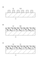
- FIGS. 1, 2 and 3 are process diagrams showing an example of a method for manufacturing a semiconductor device.
- the method shown in FIGS. 1 to 3 includes preparing a first circuit member 10 having a first substrate 11, a first electrode 12 and a first insulating film 13, preparing a second circuit member 20 having a second substrate 21, a second electrode 22 and a second insulating film 23, and heating and pressurizing the first circuit member 10 and the second circuit member 20, thereby bonding the first circuit member 10 and the second circuit member 20 so that the first insulating film 13 and the second insulating film 23 are bonded and the first electrode 12 and the second electrode 22 are bonded.
- At least one of the first substrate 11 and the second substrate 21 can be a semiconductor substrate having a circuit surface.
- a semiconductor device 1 is formed, which is a bonded body of the first circuit member 10 and the second circuit member 20.
- the first substrate 11 may be a semiconductor wafer
- the second substrate 21 may be a semiconductor chip.
- a plurality of second circuit members 20 each having a semiconductor chip may be bonded to one first circuit member 10 having a semiconductor wafer.
- the semiconductor wafer (first substrate 11) of the resulting bonded body may be singulated into a plurality of semiconductor chips.
- the semiconductor substrate may be, for example, a silicon substrate.
- the first circuit member 10 or the second circuit member 20 is not a semiconductor substrate, it may be any of various wiring substrates (for example, an interposer).
- the first electrode 12 and the first insulating film 13 are provided on the first substrate 11.
- the first substrate 11 is a semiconductor substrate having a circuit surface
- the first electrode 12 and the first insulating film 13 are provided on the circuit surface.
- the first insulating film 13 forms a plurality of openings 13a that are through holes through which the first substrate 11 is exposed, and the first electrode 12 is provided within the openings 13a.
- the second electrode 22 and the second insulating film 23 are provided on the second substrate 21.
- the second substrate 21 is a semiconductor substrate
- the second electrode 22 and the second insulating film 23 are provided on the circuit surface.
- the second insulating film 23 forms a plurality of openings 23a that are through holes through which the second substrate 21 is exposed, and the second electrode 22 is provided within the openings 23a.
- the shapes of the first electrode 12 and the second electrode 22 are not particularly limited, but some or all of these electrodes are arranged so that the first electrode 12 and the second electrode 22 face each other and are joined.
- the width of the first electrode 12 and the second electrode 22 may be, for example, 1 ⁇ m or more or 100 ⁇ m or more, and may be 300 ⁇ m or less or 30 ⁇ m or less.
- the width here means the maximum width of each electrode in a direction parallel to the main surface (circuit surface) of the first substrate 11 or the second substrate 21.
- the spacing between adjacent first electrodes 12 and the spacing between adjacent second electrodes 22 may be, for example, 1 ⁇ m or more or 100 ⁇ m or more, and may be 300 ⁇ m or less or 30 ⁇ m or less.
- the height of the first electrode 12 and the second electrode 22 may be, for example, 1 ⁇ m or more or 10 ⁇ m or more, and may be 100 ⁇ m or less or 10 ⁇ m or less.
- the height of the first electrode 12 may be the same as or different from the thickness of the first insulating film 13.
- the height of the second electrode 22 may be the same as or different from the thickness of the second insulating film 23.
- At least one of the first insulating film 13 and the second insulating film 23 can be an organic insulating film containing a cured product of a curable resin composition (hereinafter also referred to as a "curable maleimide resin composition") containing a maleimide compound having a maleimide group and an allyl compound having an allyl group.
- the organic insulating film containing the cured product of the curable maleimide resin composition can be well bonded to other insulating films by heating and pressurization. Many maleimide groups, allyl groups, or functional groups derived from these may be present on the surface of the organic insulating film containing the cured product of the curable maleimide resin composition.
- the organic insulating film can exhibit good bonding properties without necessarily requiring an activation treatment such as a plasma treatment.
- an activation treatment such as a plasma treatment.
- a more detailed example of the curable maleimide resin composition will be described later.
- both the first insulating film 13 and the second insulating film 23 are organic insulating films that contain a cured product of a curable maleimide resin composition, particularly good bonding properties are likely to be exhibited.
- either the first insulating film 13 or the second insulating film 23 may be an organic insulating film other than one that contains a cured product of a curable maleimide resin composition, or may be an inorganic insulating film.
- the first circuit member 10 can be prepared by a method including providing a plurality of columnar first electrodes 12 on one main surface 11S of the first substrate 11 as shown in FIG. 1 and FIG. 2, forming a resin film 13A containing a curable resin composition (curable maleimide resin composition) and covering the first electrode 12 on the main surface 11S of the first substrate 11 on the first electrode 12 side, curing the resin film 13A to form the first insulating film 13, which is an organic insulating film, and polishing the first insulating film 13 from the side opposite the first substrate 11 to form an opening 13a in the first insulating film 13 that exposes the first electrode 12.
- a curable resin composition curable maleimide resin composition
- the first electrode 12 is formed from a conductive material that contains a metal such as copper.
- the first electrode 12 that contains a metal can be formed by a conventional method such as plating.
- a resin film 13A containing a curable resin composition is formed on the main surface 11S of the first substrate 11 on the first electrode 12 side.
- the resin film 13A is formed, for example, by applying a curable resin composition having fluidity.
- the curable resin composition having fluidity may contain a solvent.
- the resin film 13A can be formed by heating the applied curable resin composition to remove the solvent. The heating temperature for removing the solvent may be, for example, 60°C or higher and 150°C or lower.
- the resin film 13A may be formed so as to cover the entire first electrode 12 while filling the gaps between the multiple first electrodes 12.
- the formed resin film 13A is hardened by heating.
- the resin film 13A is hardened to form a first insulating film 13 (organic insulating film), which is a hardened product of the hardenable resin composition.
- Heating causes the ene reaction between the maleimide group and the allyl group, the Diels-Alder reaction accompanied by the addition of the maleimide group, and radical polymerization to proceed, forming a hardened product. Since the hardening proceeds mainly by the addition reaction, volatile matter due to the elimination component is unlikely to be generated. In addition, since the hardening proceeds at a relatively low temperature, thermal damage to the semiconductor substrate, etc. can be reduced.
- the heating temperature for hardening the resin film 13A may be, for example, 170°C or higher and 260°C or lower.
- the heating time for hardening the resin film 13A may be, for example, 60 minutes or higher and 180 minutes or lower.
- the first insulating film 13 When the formed first insulating film 13 covers the first electrode 12, the first insulating film 13 is polished from the side opposite the first substrate 11.
- a polishing method for example, a normal method such as chemical mechanical polishing (CMP) can be used.
- CMP chemical mechanical polishing
- a part of the first insulating film 13 is removed, and an opening 13a in the first insulating film 13 where the first electrode 12 is exposed is formed.
- a part of the first electrode 12 is also removed by polishing, so that the surface of the tip of the first electrode 12 (the surface opposite the first substrate 11) is flattened.
- the height of the first electrode 12 may be greater than the thickness of the first insulating film 13 in the first circuit member 10 after polishing.
- the difference between the height of the first electrode 12 and the thickness of the first insulating film 13 may be adjusted taking into account the difference in the linear thermal expansion coefficients of the first electrode 12 and the first insulating film 13.
- the difference between the height of the first electrode 12 and the thickness of the first insulating film 13 may be, for example, 0.1 ⁇ m or more and 0.5 ⁇ m or less.
- the surface of the tip of the first electrode 12 may have a surface roughness Ra of 1 nm or less.
- the surface of the tip of the second electrode 22 may also have a similar surface roughness Ra.
- the surface roughness Ra here is the arithmetic mean roughness (Ra) defined in JIS B 0601-2001.
- the second circuit member 20 can be prepared in a similar manner.
- the shape (including the height, thickness, and surface roughness Ra) of the second electrode 22 and the second insulating film 23 may be the same as that of the first electrode 12 and the first insulating film 13.
- the prepared first circuit member 10 and second circuit member 20 are aligned so that the first electrode 12 and second electrode 22 to be joined face to face.
- the first circuit member 10 and second circuit member 20 are heated and pressurized to bond the first electrode 12 and second electrode 22 together, and to bond the first circuit member 10 and second circuit member 20 together so that the first insulating film 13 and second insulating film 23 are bonded together.
- the bonding of the first electrode 12 and the second electrode 22 and the bonding of the first insulating film 13 and the second insulating film 23 may proceed simultaneously or sequentially.
- the first circuit member 10 and the second circuit member 20 may be further heated and pressurized to bond the first electrode 12 and the second electrode 22.
- the conditions of heating and pressurization for bonding are adjusted so that the insulating film and the electrodes are properly bonded.
- the heating temperature for bonding may be 150°C or more and 250°C or less
- the pressure for bonding may be 1.0 MPa or more and 5.0 MPa or less.
- the heating and pressurization time may be, for example, 10 seconds or more and 1 hour or less.
- the curable resin composition used for forming the organic insulating film (first insulating film 13 and/or second insulating film 23) in the above-mentioned production method can be a curable maleimide resin composition containing a maleimide compound having a maleimide group and an allyl compound having an allyl group.
- the maleimide compound is a compound having one or more maleimide groups. From the standpoint of improving the heat resistance and reducing the thermal expansion coefficient of the cured product, the curable maleimide resin composition may contain a maleimide compound having two or more maleimide groups.
- the maleimide compound may have an imide group containing a nitrogen atom directly bonded to a cyclic group (e.g., an aromatic group).
- a cyclic group e.g., an aromatic group
- the maleimide compound in the curable maleimide resin composition may be represented by the following formula (Ia) or (Ib):
- the compound may include a compound represented by the formula:
- Q 1 and Q 2 each independently represent a cyclic group which may have a substituent, and L 1 represents a divalent organic group or a single bond.
- Q 1 and Q 2 each independently may be an aromatic group (e.g., a phenylene group).
- L 1 may be a group containing one or more cyclic groups (excluding a maleimide group) selected from a monocycle, a condensed ring, a non-condensed bridged ring, and a spiro ring which may have a substituent, a linear alkylene group which may have a substituent (e.g., a methylene group, a propane-1,3-diyl group), a propane-2,2-diyl group which may have a substituent, or a single bond.
- cyclic groups excluding a maleimide group
- L 1 may have two or more cyclic groups and a single bond or a divalent organic group (e.g., a methylene group which may have a substituent, a propane-2,2-diyl group which may have a substituent) which connects the two or more cyclic groups.
- L 1 may further have a methylene group which connects the cyclic group to Q 1 or Q 2 .
- the cyclic group in L 1 may be substituted with, for example, a methyl group or a maleimide group.
- L 1 may have a cyclic group formed by removing one or more hydrogen atoms from benzene, 2,3-dihydro-1H-indene, or succinimide.
- Q3 represents a cyclic group which may have a substituent.
- Q3 may be an aromatic group (e.g., a phenylene group).
- the cyclic group in Q3 may be substituted with, for example, a methyl group or a maleimide group.
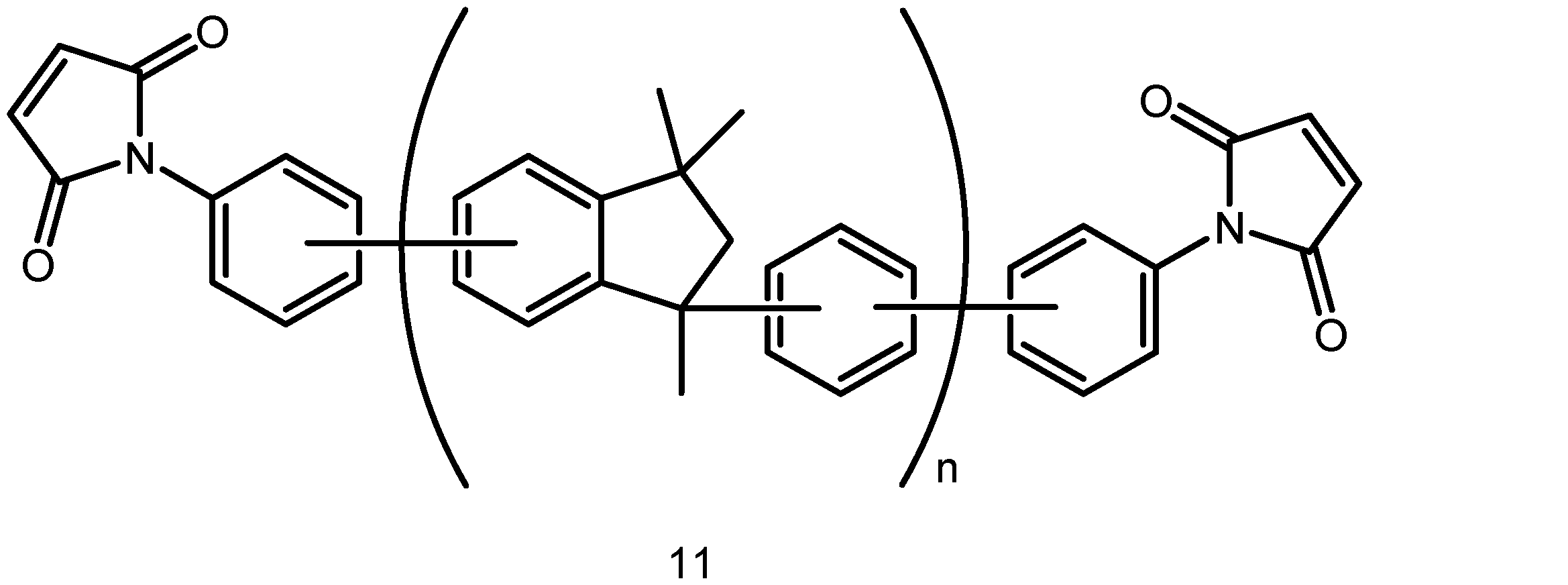
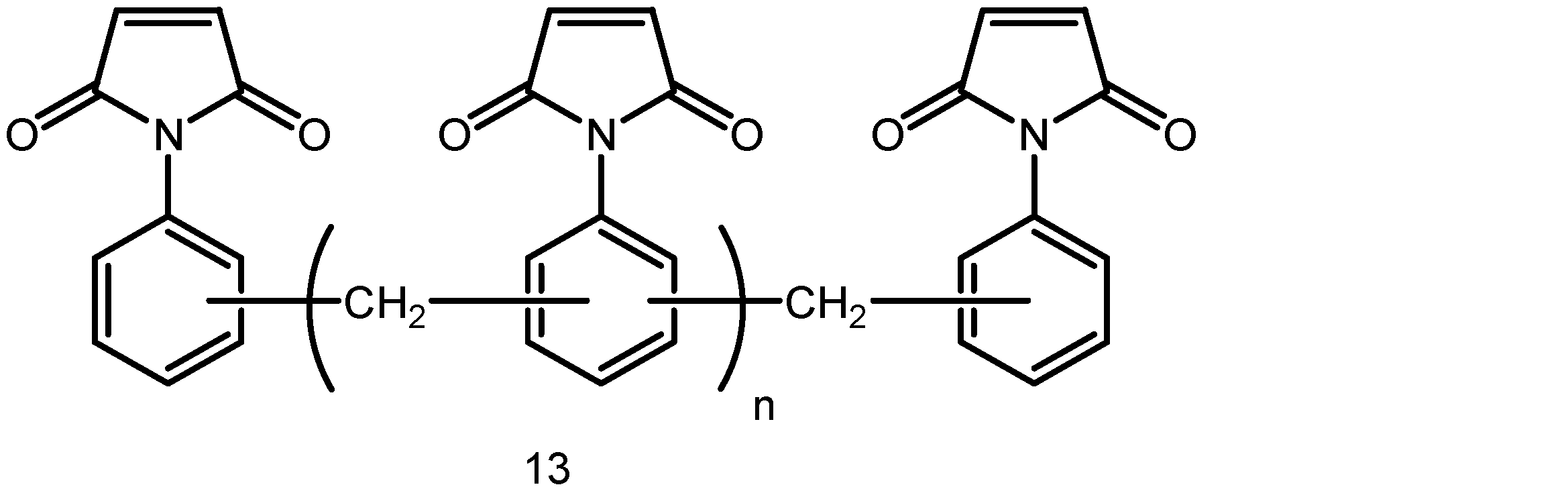
- maleimide compounds include compounds represented by the following formulas 11, 12, 13, and 14. In these formulas, n is an integer of 1 or more.
- maleimide compounds include NE-X-9470S (product name: DIC), MIR-3000-70MT (product name: Nippon Kayaku), BMI-2300 (product name: Daiwa Kasei Kogyo), BMI-5100 (product name: Daiwa Kasei Kogyo), BMI-80 (product name: Daiwa Kasei Kogyo), BMI (product name: Daiwa Kasei Kogyo), and SFR-2300MR-T (product name: Showa Denko Materials).
- the allyl compound is a compound having one or more allyl groups (2-propenyl group, -CH 2 CH ⁇ CH 2 ). From the standpoint of improving the heat resistance and reducing the thermal expansion coefficient of the cured product, the curable maleimide resin composition may contain an allyl compound having two or more allyl groups.
- the allyl compound may include a compound having a cyclic group and an allyl group or an allyloxy group directly bonded to the cyclic group.
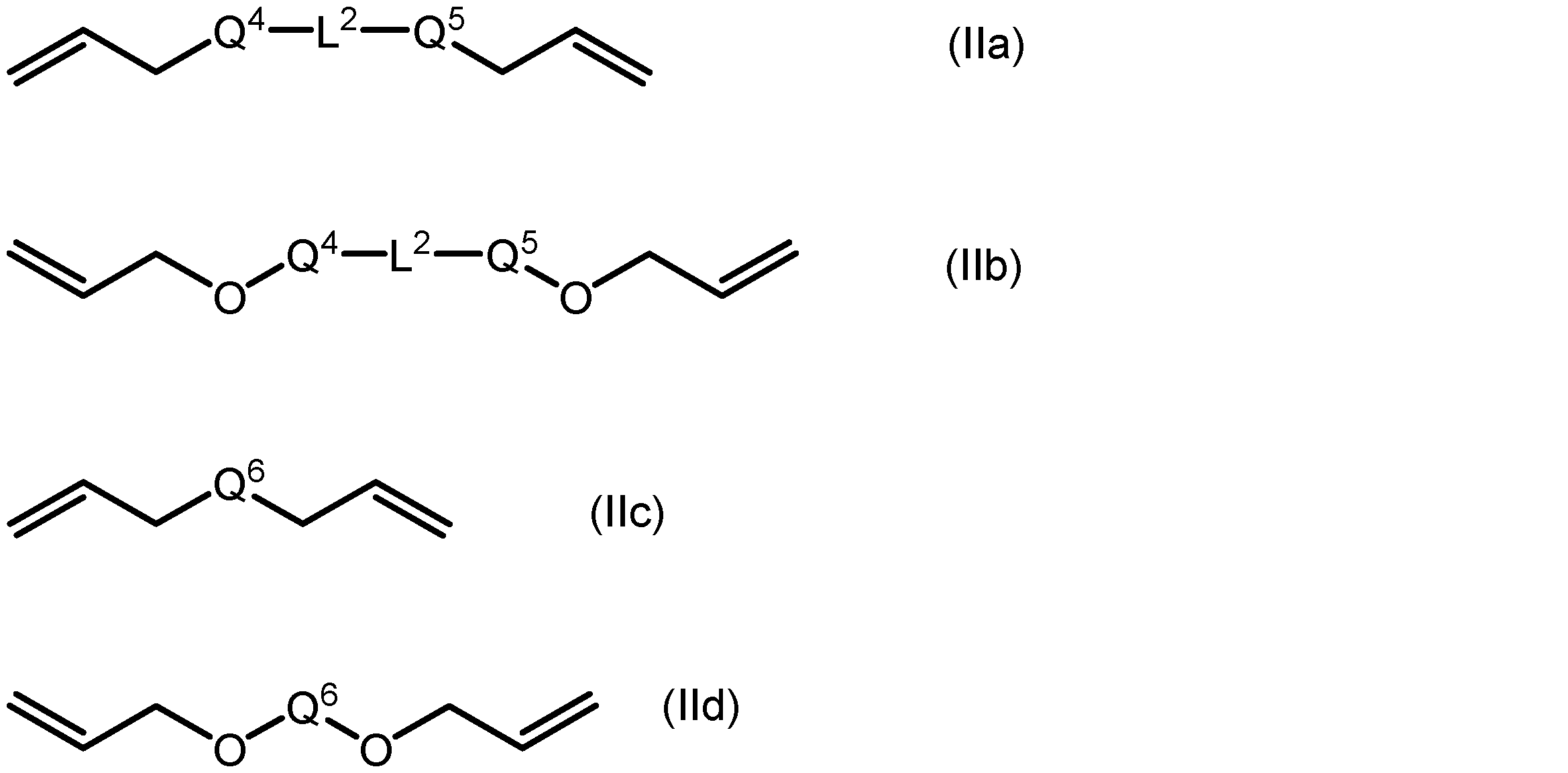
- the allyl compound in the curable maleimide resin composition may be represented by the following formula (IIa), (IIb), (IIc), or (IId):
- the compound may include a compound represented by the formula:
- Q 4 and Q 5 each independently represent a cyclic group which may have a substituent, and L 2 represents a divalent organic group or a single bond.
- Q 4 and Q 5 may each independently represent a group obtained by removing one or more hydrogen atoms from benzene, isocyanuric acid, or nadimide.
- L 2 may be a group containing one or more cyclic groups (excluding maleimide groups) which may have a substituent selected from a monocycle, a condensed ring, a non-condensed bridged ring, and a spiro ring, a linear alkylene group which may have a substituent (e.g., a methylene group, a propane-1,3-diyl group), a propane-2,2-diyl group which may have a substituent, or a single bond.
- cyclic groups excluding maleimide groups
- L 2 may have two or more cyclic groups and a single bond or a divalent organic group (e.g., a methylene group which may have a substituent, a propane-2,2-diyl group which may have a substituent) which connects the two or more cyclic groups.
- L2 may further have a methylene group linking the cyclic group to Q4 or Q5 .
- the cyclic group in L2 may be substituted with a substituent selected from, for example, a methyl group, a hydroxyl group, and an allyl group.
- L2 may have a phenylene group which may have a substituent.
- Q6 represents a cyclic group which may have a substituent.
- Q6 may be an aromatic group (e.g., a phenylene group) or a group in which one or more hydrogen atoms have been removed from isocyanuric acid.
- the cyclic group in Q3 may be substituted with, for example, a methyl group or an allyl group.
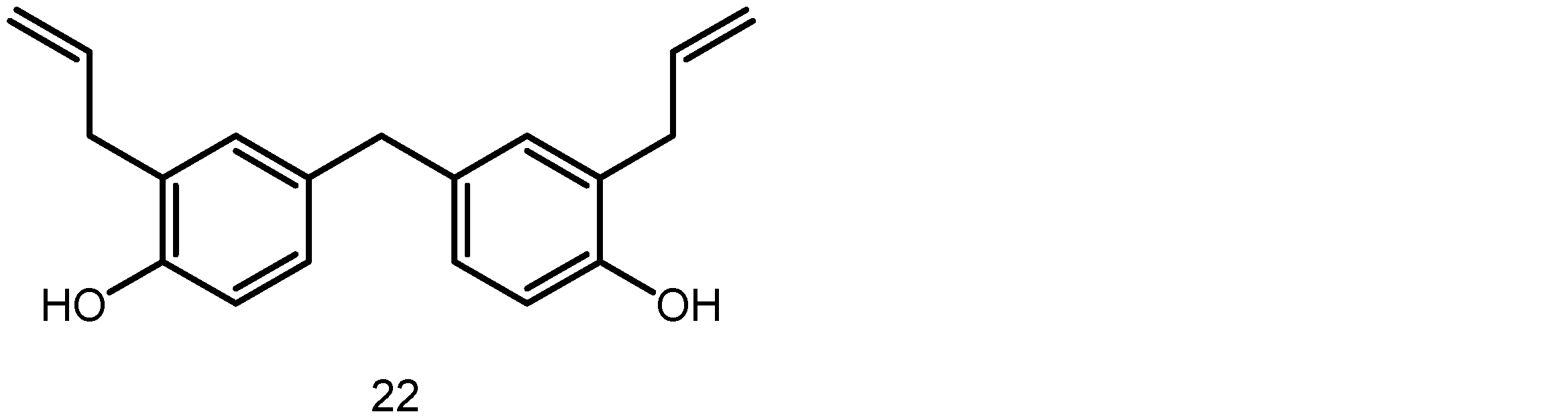
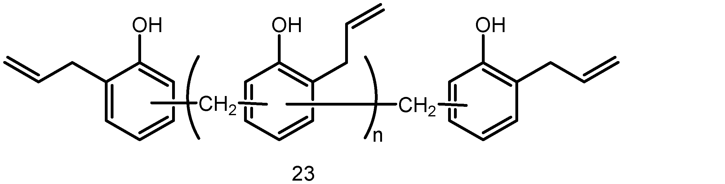
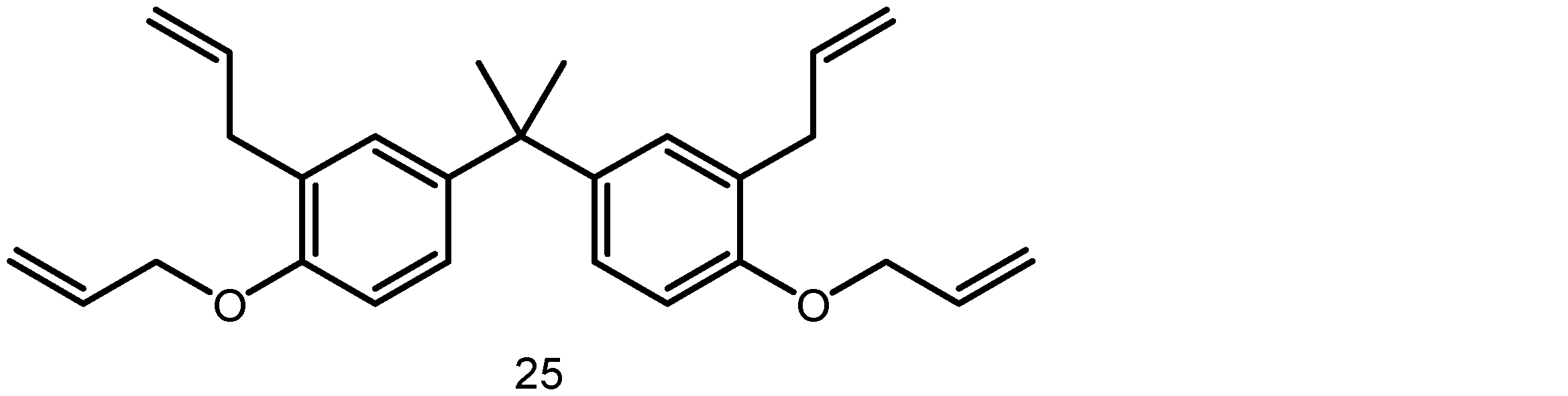
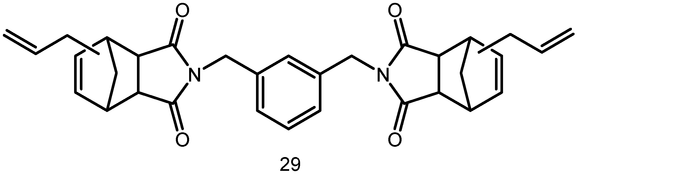
- allyl compound examples include compounds represented by the following formulas 21, 22, 23, 24, 25, 26, 27, 28, and 29.
- n represents an integer of 1 or more.
- allyl compounds include DABPA (trade name, Kanto Chemical), DA-BPF (trade name, Yokkaichi Chemical), LVA01 (trade name, Gun-ei Chemical), BPA-AE (trade name, Konishi Chemical), BANI-X (trade name, Maruzen Petrochemical), BANI-M (trade name, Maruzen Petrochemical), FATC-809 (trade name, Gun-ei Chemical), FATC-809AP (trade name, Gun-ei Chemical), DAIC (trade name, Shikoku Chemical Industry), and DD-1 (trade name, Shikoku Chemical Industry).
- the content of the allyl compound may be 10% by mass or more and 70% by mass or less, based on the total amount of the maleimide compound and the allyl compound.
- the content of the allyl compound may be 15% by mass or more, 20% by mass or more, 25% by mass or more, or 30% by mass or more, based on the total amount of the maleimide compound and the allyl compound, and may be 65% by mass or less, 60% by mass or less, or 55% by mass or less.
- the curable maleimide resin composition may further contain a component that initiates or accelerates the reaction between the maleimide compound and the allyl compound.
- the curable maleimide resin composition may further contain a component that reduces the dielectric tangent of the cured product (hereinafter referred to as a "dielectric tangent adjuster").
- the dielectric tangent adjuster may be, for example, a compound represented by the following formula (IIIa), (IIIb), or (IIIc):
- R 11 , R 14 and R 15 each independently represent a hydrogen atom, a methyl group or a t-butyl group
- R 12 and R 13 each independently represent a hydrogen atom, a hydroxyl group or an organic group having 1 to 30 carbon atoms
- Z 1 represents an organic group having 7 to 80 carbon atoms containing at least one heteroatom selected from the group consisting of sulfur, phosphorus, oxygen and nitrogen, or an organic group having 2 to 15 carbon atoms containing a carbonyl group.
- R 16 , R 19 , R 20 , R 21 , R 22 and R 25 each independently represent a hydrogen atom, a methyl group or a t-butyl group
- R 17 , R 18 , R 23 and R 24 each independently represent a hydrogen atom, a hydroxyl group or an organic group having 1 to 30 carbon atoms
- Z 2 represents a divalent organic group having 1 to 50 carbon atoms containing at least one heteroatom selected from the group consisting of sulfur, phosphorus, oxygen and nitrogen, or a divalent organic group having 1 to 75 carbon atoms.
- R 26 , R 29 , R 30 , R 31 , R 34 , R 35 , R 36 , R 37 and R 40 each independently represent a hydrogen atom, a methyl group or a t-butyl group
- R 27 , R 28 , R 32 , R 33 , R 38 and R 39 each independently represent a hydrogen atom, a hydroxyl group or an organic group having 1 to 30 carbon atoms
- Z 3 represents a trivalent organic group having 1 to 50 carbon atoms containing at least one heteroatom selected from the group consisting of sulfur, phosphorus, oxygen and nitrogen, or a trivalent organic group having 1 to 50 carbon atoms.
- the content of the dielectric loss tangent adjuster may be 1% by mass or more and 50% by mass or less based on the total amount of the maleimide compound and the allyl compound.
- the content of the dielectric loss tangent adjuster may be 2% by mass or more or 5% by mass or more based on the total amount of the maleimide compound and the allyl compound, and may be 50% by mass or less or 40% by mass or less.
- the curable maleimide resin composition may further contain a solvent that dissolves or disperses the maleimide compound and the allyl compound.
- a solvent that dissolves or disperses the maleimide compound and the allyl compound.
- the solvent include ⁇ -butyrolactone, cyclohexanone, cyclopentanone, mesitylene, N,N-dimethylformamide, propylene glycol monomethyl ether acetate, and ethyl lactate.
- the curable maleimide resin composition may further include an adhesion aid.
- the adhesion aid may include, for example, a silane coupling agent, an aluminum-based adhesion aid, or a combination thereof.
- silane coupling agents include ⁇ -aminopropyldimethoxysilane, N-( ⁇ -aminoethyl)- ⁇ -aminopropylmethyldimethoxysilane, ⁇ -glycidoxypropylmethyldimethoxysilane, ⁇ -mercaptopropylmethyldimethoxysilane, 3-methacryloxypropyldimethoxymethylsilane, 3-methacryloxypropyltrimethoxysilane, dimethoxymethyl-3-piperidinopropylsilane, diethoxy-3-glycidoxypropylmethylsilane, N-( 3-diethoxymethylsilylpropyl)succinimide, N-[3-(triethoxysilyl)propyl]phthalamic acid, benzophenone-3,3'-bis(N-[3-triethoxysilyl]propylamide)-4,4'-dicarboxylic acid, benzene-1,4-bis
- aluminum-based adhesive aids examples include aluminum tris(ethylacetoacetate), aluminum tris(acetylacetonate), and ethylacetoacetate aluminum diisopropylate.
- the content of the adhesive aid may be, for example, 0.5% by mass or more and 25% by mass or less based on the total amount of the maleimide compound and the allyl compound.
- the curable maleimide resin composition may further include a polymerization inhibitor.
- polymerization inhibitors include hydroquinone, N-nitrosodiphenylamine, p-tert-butylcatechol, 4-methoxyphenol, phenothiazine, N-phenylnaphthylamine, ethylenediaminetetraacetic acid, 1,2-cyclohexanediaminetetraacetic acid, glycol ether diaminetetraacetic acid, 2,6-di-tert-butyl-p-methylphenol, 5-nitroso-8-hydroxyquinoline, 1-nitroso-2-naphthol, 2-nitroso-1-naphthol, 2-nitroso-5-(N-ethyl-N-sulfopropylamino)phenol, N-nitroso-N-phenylhydroxylamine ammonium salt, and N-nitroso-N(1-naphthyl)hydroxylamine ammonium salt.
- the content of the polymerization inhibitor may be 0.005% by mass or more and 12% by mass or less based on the total amount of the maleimide compound and the allyl compound.
- the curable maleimide resin composition may further include an azole compound.
- the azole compound include 1H-triazole, 5-methyl-1H-triazole, 5-ethyl-1H-triazole, 4,5-dimethyl-1H-triazole, 5-phenyl-1H-triazole, 4-t-butyl-5-phenyl-1H-triazole, 5-hydroxyphenyl-1H-triazole, phenyltriazole, p-ethoxyphenyltriazole, 5-phenyl-1-(2-dimethylaminoethyl)triazole, 5-benzyl-1H-triazole, hydroxyphenyltriazole, 1,5-dimethyltriazole, 4,5-diethyl-1H-triazole, 1H-benzotriazole, 2-(5-methyl-2-hydroxyphenyl)benzotriazole, 2-[2-hydroxy-3,5-bis( ⁇ , ⁇ -dimethylbenzyl)phenyl]-benzotriazole, and
- the content of the azole compound may be from 0.1% by mass to 20% by mass, or from 0.5% by mass to 5% by mass, based on the total amount of the maleimide compound and the allyl compound.
- the curable maleimide resin composition may contain a hindered phenol compound.
- the hindered phenol compound include 2,6-di-t-butyl-4-methylphenol, 2,5-di-t-butyl-hydroquinone, octadecyl-3-(3,5-di-t-butyl-4-hydroxyphenyl)propionate, isooctyl-3-(3,5-di-t-butyl-4-hydroxyphenyl)propionate, 4,4'-methylenebis(2,6-di-t-butylphenol), 4,4'-thio-bis(3-methyl-6-t-butylphenol), 4,4'-butylyl 1,6-hexanediol-bis[3-(3,5-di-t-butyl-4-hydroxyphenyl)propionate], 2,2-thio-diethylenebis[3-(3,5-di-t-butyl-4-hydroxyphenyl)propionate], N
- the content of the hindered phenol compound may be from 0.1% by mass to 20% by mass, or from 0.5% by mass to 10% by mass, based on the total amount of the maleimide compound and the allyl compound.
- the curable maleimide resin composition may contain an organic titanium compound.
- the organic titanium compound may be, for example, a titanium chelate compound having two or more alkoxy groups, a tetraalkoxy titanium compound, a titanocene compound, a monoalkoxy titanium compound, a titanium oxide compound, a titanium tetraacetylacetonate compound, a titanate coupling agent, or a combination thereof.
- titanium chelate compounds having two or more alkoxy groups include titanium bis(triethanolamine) diisopropoxide, titanium di(n-butoxide) bis(2,4-pentanedionate), titanium diisopropoxide bis(2,4-pentanedionate), titanium diisopropoxide bis(tetramethylheptanedionate), and titanium diisopropoxide bis(ethylacetoacetate).
- tetraalkoxytitanium compounds include titanium tetra(n-butoxide), titanium tetraethoxide, titanium tetra(2-ethylhexoxide), titanium tetraisobutoxide, titanium tetraisopropoxide, titanium tetramethoxide, titanium tetramethoxypropoxide, titanium tetramethylphenoxide, titanium tetra(n-nonyloxide), titanium tetra(n-propoxide), titanium tetrastearyloxide, and titanium tetrakis[bis ⁇ 2,2-(allyloxymethyl)butoxide ⁇ ].
- titanocene compounds include pentamethylcyclopentadienyltitanium trimethoxide, bis( ⁇ 5-2,4-cyclopentadiene-1-yl)bis(2,6-difluorophenyl)titanium, and bis( ⁇ 5-2,4-cyclopentadiene-1-yl)bis(2,6-difluoro-3-(1H-pyrrol-1-yl)phenyl)titanium.
- Examples of monoalkoxytitanium compounds include titanium tris(dioctylphosphate) isopropoxide and titanium tris(dodecylbenzenesulfonate) isopropoxide.
- titanium oxide compounds include titanium oxide bis(pentanedionate), titanium oxide bis(tetramethylheptanedionate), and phthalocyanine titanium oxide.
- titanium tetraacetylacetonate compound is titanium tetraacetylacetonate.
- titanate coupling agent is isopropyl tridodecylbenzenesulfonyl titanate.
- the content of the organotitanium compound may be from 0.05% by mass to 10% by mass, or from 0.1% by mass to 2% by mass, based on the total amount of the maleimide compound and the allyl compound.
- maleimide compound Phenylmethanemaleimide (compound of formula 13, BMI-2300, Daiwa Chemical Industry Co., Ltd.) 4,4'-diphenylmethane bismaleimide (compound of formula 14, BMI, Daiwa Chemical Industry Co., Ltd.) Allyl compound/arylphenol resin (compound of formula 23, LVA01, Gun-ei Chemical Industry Co., Ltd.) 2,2'-diallyl bisphenol A (DABPA, Kanto Chemical Co., Ltd.) Compound of formula 25 (BATE, synthesized according to standard methods) Bisallylnadimide (compound of formula 29, BANI-M, Maruzen Petrochemical Co., Ltd.)
- Example 1 (1) Evaluation of Thermal Properties of Organic Insulating Film A maleimide compound and an allyl compound in the compounding ratio (parts by mass) shown in Table 1 were mixed while being melted by heating to prepare a resin composition.
- the resin composition was applied to a substrate with a bar coater to form a resin film.
- the resin film was heated at 175°C for 1 hour, at 200°C for 30 minutes, and at 250°C for 1 hour in that order.
- the resin film was cured by this heating.
- An organic insulating film having a thickness of 100 ⁇ m was formed by curing the resin film.
- Tg Glass transition temperature
- CTE Coefficient of linear thermal expansion
- Example 2 The curable resin composition of Example 2 was applied onto a silicon wafer (diameter: 8 inches) by a spin coater. The coating film was heated in the following order: 175°C for 1 hour, 200°C for 30 minutes, and 250°C for 1 hour. This heating caused the resin film to harden. The resin film was hardened to form an organic insulating film having a thickness of 10 ⁇ m. The silicon wafer was cut into individual pieces together with the organic insulating film by blade dicing to obtain a lower test piece having a size of 8 mm x 8 mm and an upper test piece having a size of 4 mm x 4 mm.
- the upper test piece was superimposed on the center of the organic insulating film of the lower test piece in a direction in which the organic insulating films contact each other.
- the laminate of the lower test piece and the upper test piece was heated to 250°C and pressurized at a pressure of 2.6 MPa for 1 hour.
- This heating and pressurization formed a bonded body in which the organic insulating film of the lower test piece and the organic insulating film of the upper test piece were bonded to each other.
- the shear strength at 60°C was measured by a peel test in which stress was applied to the upper test piece of the bonded structure along the bonding surface of the organic insulating film.
- Examples 5 to 8 A maleimide compound and an allyl compound in the compounding ratio (parts by mass) shown in Table 2 were mixed while being melted by heating to prepare a resin composition.
- the resin composition was applied onto a substrate with a bar coater to form a resin film.
- the resin film was heated at 175°C for 1 hour, at 200°C for 30 minutes, and at 250°C for 1 hour, in that order.
- the resin film was cured by this heating.
- An organic insulating film having a thickness of 100 ⁇ m was formed by the curing of the resin film.
- the Tg of the organic insulating film was measured by the same method as in Examples 1 to 4.
- 1...semiconductor device 10...first circuit member, 11...first substrate, 12...first electrode, 13...first insulating film, 13a, 23a...opening, 13A...resin film, 20...second circuit member, 21...second substrate, 22...second electrode, 23...second insulating film.
Landscapes
- Addition Polymer Or Copolymer, Post-Treatments, Or Chemical Modifications (AREA)
- Formation Of Insulating Films (AREA)
- Engineering & Computer Science (AREA)
- Manufacturing & Machinery (AREA)
Abstract
Description
[1]
第一基板、第一電極及び第一絶縁膜を有する第一回路部材であって、前記第一電極及び前記第一絶縁膜が前記第一基板上に設けられ、前記第一絶縁膜が開口を形成し、前記開口内に前記第一電極が設けられている、第一回路部材を準備することと、
第二基板、第二電極及び第二絶縁膜を有する第二回路部材であって、前記第二電極及び前記第二絶縁膜が前記第二基板上に設けられ、前記第二絶縁膜が開口を形成し、前記開口内に前記第二電極が設けられている、第二回路部材を準備することと、
前記第一回路部材及び前記第二回路部材を加熱及び加圧し、それにより、前記第一絶縁膜と前記第二絶縁膜とが接合されるとともに、前記第一電極と前記第二電極とが接合されるように、前記第一回路部材と前記第二回路部材とを接合することと、
を備え、
前記第一基板又は前記第二基板のうち少なくとも一方が、回路面を有する半導体基板であり、
前記第一基板が回路面を有する半導体基板であるとき、前記回路面上に前記第一電極及び前記第一絶縁膜が設けられ、前記第二基板が回路面を有する半導体基板であるとき、前記回路面上に前記第二電極及び前記第二絶縁膜が設けられ、
前記第一絶縁膜又は前記第二絶縁膜のうち少なくとも一方が、マレイミド基を有するマレイミド化合物と、アリル基を有するアリル化合物とを含む硬化性樹脂組成物の硬化物を含む有機絶縁膜である、
半導体装置を製造する方法。
[2]
前記第一絶縁膜が前記有機絶縁膜であるとき、前記第一回路部材が、前記第一基板上に前記硬化性樹脂組成物を含む樹脂膜を形成することと、前記樹脂膜を硬化させることとを含む方法によって準備され、
前記第二絶縁膜が前記硬化性樹脂組成物の硬化物であるとき、前記第二回路部材が、前記第二基板上に前記硬化性樹脂組成物を含む樹脂膜を形成することと、前記樹脂膜を硬化させることとを含む方法によって準備される、
[1]に記載の方法。
[3]
前記第一絶縁膜及び前記第二絶縁膜が前記有機絶縁膜である、[1]又は[2]に記載の方法。
[4]
第一基板、第一電極及び第一絶縁膜を有する第一回路部材であって、前記第一電極及び前記第一絶縁膜が前記第一基板上に設けられ、前記第一絶縁膜が開口を形成し、前記開口内に前記第一電極が設けられている、第一回路部材と、
前記第一回路部材と接合された、第二基板、第二電極及び第二絶縁膜を有する第二回路部材であって、前記第二電極及び前記第二絶縁膜が前記第二基板上に設けられ、前記第二絶縁膜が開口を形成し、前記開口内に前記第二電極が設けられている、第二回路部材と、
を備え、
前記第一絶縁膜と前記第二絶縁膜とが接合されるとともに、前記第一電極と前記第二電極とが接合されるように、前記第一回路部材と前記第二回路部材とが接合されており、
前記第一基板又は前記第二基板のうち少なくとも一方が、回路面を有する半導体基板であり、
前記第一基板が回路面を有する半導体基板であるとき、前記回路面上に前記第一電極及び前記第一絶縁膜が設けられ、前記第二基板が回路面を有する半導体基板であるとき、前記回路面上に前記第二電極及び前記第二絶縁膜が設けられており、
前記第一絶縁膜又は前記第二絶縁膜のうち少なくとも一方が、マレイミド基を有するマレイミド化合物と、アリル基を有するアリル化合物とを含む硬化性樹脂組成物の硬化物を含む有機絶縁膜である、
半導体装置。
[5]
前記第一絶縁膜及び前記第二絶縁膜が前記有機絶縁膜である、[4]に記載の半導体装置。
[6]
マレイミド基を有するマレイミド化合物と、アリル基を有するアリル化合物と、を含み、[1]~[3]のいずれかに記載の方法において有機絶縁膜を形成するために用いられる、硬化性樹脂組成物。
[7]
マレイミド基を有するマレイミド化合物と、アリル基を有するアリル化合物と、を含む硬化性樹脂組成物の、[1]~[3]のいずれかに記載の方法によって半導体装置を製造するための応用。
図1、図2及び図3は、半導体装置を製造する方法の一例を示す工程図である。図1~3に示される方法は、第一基板11、第一電極12及び第一絶縁膜13を有する第一回路部材10を準備することと、第二基板21、第二電極22及び第二絶縁膜23を有する第二回路部材20を準備することと、第一回路部材10及び第二回路部材20を加熱及び加圧し、それにより、第一絶縁膜13と第二絶縁膜23とが接合されるとともに、第一電極12と第二電極22とが接合されるように、第一回路部材10と第二回路部材20とを接合することとを含む。第一基板11又は第二基板21のうち少なくとも一方が、回路面を有する半導体基板であることができる。通常、半導体基板の回路面側に集積回路が設けられている。この方法により、第一回路部材10と第二回路部材20との接合体である半導体装置1が形成される。例えば、第一基板11が半導体ウェハで、第二基板21が半導体チップであってもよい。半導体ウェハを有する1枚の第一回路部材10に、半導体チップを有する複数の第二回路部材20が接合されてもよい。その場合、得られた接合体の半導体ウェハ(第一基板11)を複数の半導体チップに個片化してもよい。半導体基板は、例えばシリコン基板であってもよい。第一回路部材10又は第二回路部材20が半導体基板でないとき、これらは各種の配線基板(例えばインターポーザ)であってもよい。
上述の製造方法において有機絶縁膜(第一絶縁膜13及び/又は第二絶縁膜23)を形成するために用いられる硬化性樹脂組成物は、マレイミド基を有するマレイミド化合物と、アリル基を有するアリル化合物とを含む硬化性マレイミド樹脂組成物であることができる。








原料
以下のマレイミド化合物及びアリル化合物を準備した。
マレイミド化合物
・フェニルメタンマレイミド(式13の化合物、BMI-2300、大和化成工業株式会社)
・4,4’-ジフェニルメタンビスマレイミド(式14の化合物、BMI、大和化成工業株式会社)
アリル化合物
・アリールフェノール樹脂(式23の化合物、LVA01、群栄化学工業株式会社)
・2,2’-ジアリルビスフェノールA(DABPA、関東化学株式会社)
・式25の化合物(BATE、常法に従って合成された)
・ビスアリルナジイミド(式29の化合物、BANI-M、丸善石油化学株式会社)
(1)有機絶縁膜の熱特性評価
表1に示される配合比(質量部)のマレイミド化合物及びアリル化合物を加熱により溶融させながら混合して、樹脂組成物を調製した。樹脂組成物をバーコータにより基板上に塗布して、樹脂膜を形成した。樹脂膜を175℃で1時間、200℃で30分及び250℃で1時間の順に加熱した。この加熱により樹脂膜を硬化させた。樹脂膜の硬化により、厚さ100μmの有機絶縁膜が形成された。
有機絶縁膜のTgを、以下の条件の動的粘弾性測定(DMA)により測定した。Tanδが極大値を示す温度をTgとして記録した。
・周波数:10Hz
・昇温速度:5℃/分
有機絶縁膜の線熱膨張係数(CTE)をTMA法により測定した。50℃~100℃の温度範囲におけるCTEが求められた。測定結果が表1に示される。

実施例2の硬化性樹脂組成物を、シリコンウェハ(直径:8インチ)上にスピンコータによって塗布した。塗膜を175℃で1時間、200℃で30分及び250℃で1時間の順に加熱した。この加熱により樹脂膜を硬化させた。樹脂膜の硬化により厚さ10μmの有機絶縁膜が形成された。シリコンウェハを、ブレードダイシングによって有機絶縁膜とともに個片化し、8mm×8mmのサイズを有する下部用試験片と、4mm×4mmのサイズを有する上部用試験片とを得た。下部用試験片の有機絶縁膜の中央部に、上部用試験片を、有機絶縁膜同士が接する向きで重ね合わせた。その状態で、下部用試験片と上部用試験片の積層体を、250℃に加熱しながら、2.6MPaの圧力で1時間加圧した。この加熱及び加圧により、下部用試験片の有機絶縁膜と上部用試験片の有機絶縁膜とが接合した接合体が形成された。接合体の上部試験片に対して有機絶縁膜の接合面に沿った応力を加える剥離試験により、60℃におけるせん断強度を測定した。剥離試験においてシリコンウェハが破壊するモードで剥離が生じ、せん断強度は16.3MPaであった。この結果から、マレイミド化合物及びアリル化合物を含む硬化性樹脂組成物から形成された有機絶縁膜同士を接合できることが確認された。
表2に示される配合比(質量部)のマレイミド化合物及びアリル化合物を加熱により溶融させながら混合して、樹脂組成物を調製した。樹脂組成物をバーコータにより基板上に塗布して、樹脂膜を形成した。樹脂膜を175℃で1時間、200℃で30分及び250℃で1時間の順に加熱した。この加熱により樹脂膜を硬化させた。樹脂膜の硬化により、厚さ100μmの有機絶縁膜が形成された。有機絶縁膜のTgを実施例1~4と同様の方法で測定した。

Claims (6)
- 第一基板、第一電極及び第一絶縁膜を有する第一回路部材であって、前記第一電極及び前記第一絶縁膜が前記第一基板上に設けられ、前記第一絶縁膜が開口を形成し、前記開口内に前記第一電極が設けられている、第一回路部材を準備することと、
第二基板、第二電極及び第二絶縁膜を有する第二回路部材であって、前記第二電極及び前記第二絶縁膜が前記第二基板上に設けられ、前記第二絶縁膜が開口を形成し、前記開口内に前記第二電極が設けられている、第二回路部材を準備することと、
前記第一回路部材及び前記第二回路部材を加熱及び加圧し、それにより、前記第一絶縁膜と前記第二絶縁膜とが接合されるとともに、前記第一電極と前記第二電極とが接合されるように、前記第一回路部材と前記第二回路部材とを接合することと、
を備え、
前記第一基板又は前記第二基板のうち少なくとも一方が、回路面を有する半導体基板であり、
前記第一基板が回路面を有する半導体基板であるとき、前記回路面上に前記第一電極及び前記第一絶縁膜が設けられ、前記第二基板が回路面を有する半導体基板であるとき、前記回路面上に前記第二電極及び前記第二絶縁膜が設けられ、
前記第一絶縁膜又は前記第二絶縁膜のうち少なくとも一方が、マレイミド基を有するマレイミド化合物と、アリル基を有するアリル化合物とを含む硬化性樹脂組成物の硬化物を含む有機絶縁膜である、
半導体装置を製造する方法。 - 前記第一絶縁膜が前記有機絶縁膜であるとき、前記第一回路部材が、前記第一基板上に前記硬化性樹脂組成物を含む樹脂膜を形成することと、前記樹脂膜を硬化させることとを含む方法によって準備され、
前記第二絶縁膜が前記硬化性樹脂組成物の硬化物であるとき、前記第二回路部材が、前記第二基板上に前記硬化性樹脂組成物を含む樹脂膜を形成することと、前記樹脂膜を硬化させることとを含む方法によって準備される、
請求項1に記載の方法。 - 前記第一絶縁膜及び前記第二絶縁膜が前記有機絶縁膜である、請求項1又は2に記載の方法。
- 第一基板、第一電極及び第一絶縁膜を有する第一回路部材であって、前記第一電極及び前記第一絶縁膜が前記第一基板上に設けられ、前記第一絶縁膜が開口を形成し、前記開口内に前記第一電極が設けられている、第一回路部材と、
前記第一回路部材と接合された、第二基板、第二電極及び第二絶縁膜を有する第二回路部材であって、前記第二電極及び前記第二絶縁膜が前記第二基板上に設けられ、前記第二絶縁膜が開口を形成し、前記開口内に前記第二電極が設けられている、第二回路部材と、
を備え、
前記第一絶縁膜と前記第二絶縁膜とが接合されるとともに、前記第一電極と前記第二電極とが接合されるように、前記第一回路部材と前記第二回路部材とが接合されており、
前記第一基板又は前記第二基板のうち少なくとも一方が、回路面を有する半導体基板であり、
前記第一基板が回路面を有する半導体基板であるとき、前記回路面上に前記第一電極及び前記第一絶縁膜が設けられ、前記第二基板が回路面を有する半導体基板であるとき、前記回路面上に前記第二電極及び前記第二絶縁膜が設けられており、
前記第一絶縁膜又は前記第二絶縁膜のうち少なくとも一方が、マレイミド基を有するマレイミド化合物と、アリル基を有するアリル化合物とを含む硬化性樹脂組成物の硬化物を含む有機絶縁膜である、
半導体装置。 - 前記第一絶縁膜及び前記第二絶縁膜が前記有機絶縁膜である、請求項4に記載の半導体装置。
- マレイミド基を有するマレイミド化合物と、アリル基を有するアリル化合物と、を含み、請求項1又は2に記載の方法において有機絶縁膜を形成するために用いられる、硬化性樹脂組成物。
Priority Applications (5)
| Application Number | Priority Date | Filing Date | Title |
|---|---|---|---|
| KR1020257026421A KR20250134107A (ko) | 2023-02-09 | 2023-02-09 | 반도체 장치를 제조하는 방법, 반도체 장치, 및 경화성 수지 조성물 |
| PCT/JP2023/004431 WO2024166319A1 (ja) | 2023-02-09 | 2023-02-09 | 半導体装置を製造する方法、半導体装置、及び硬化性樹脂組成物 |
| CN202380092069.9A CN120642024A (zh) | 2023-02-09 | 2023-02-09 | 制造半导体装置的方法、半导体装置及固化性树脂组合物 |
| JP2024576013A JPWO2024166319A1 (ja) | 2023-02-09 | 2023-02-09 | |
| TW113104635A TW202441710A (zh) | 2023-02-09 | 2024-02-06 | 製造半導體裝置之方法、半導體裝置及固化性樹脂組成物 |
Applications Claiming Priority (1)
| Application Number | Priority Date | Filing Date | Title |
|---|---|---|---|
| PCT/JP2023/004431 WO2024166319A1 (ja) | 2023-02-09 | 2023-02-09 | 半導体装置を製造する方法、半導体装置、及び硬化性樹脂組成物 |
Publications (1)
| Publication Number | Publication Date |
|---|---|
| WO2024166319A1 true WO2024166319A1 (ja) | 2024-08-15 |
Family
ID=92262191
Family Applications (1)
| Application Number | Title | Priority Date | Filing Date |
|---|---|---|---|
| PCT/JP2023/004431 Ceased WO2024166319A1 (ja) | 2023-02-09 | 2023-02-09 | 半導体装置を製造する方法、半導体装置、及び硬化性樹脂組成物 |
Country Status (5)
| Country | Link |
|---|---|
| JP (1) | JPWO2024166319A1 (ja) |
| KR (1) | KR20250134107A (ja) |
| CN (1) | CN120642024A (ja) |
| TW (1) | TW202441710A (ja) |
| WO (1) | WO2024166319A1 (ja) |
Cited By (2)
| Publication number | Priority date | Publication date | Assignee | Title |
|---|---|---|---|---|
| WO2026033761A1 (ja) * | 2024-08-08 | 2026-02-12 | 株式会社レゾナック | ハイブリッドボンディング用硬化性樹脂組成物、及び、回路接続体を製造する方法 |
| WO2026070803A1 (ja) * | 2024-09-27 | 2026-04-02 | 富士フイルム株式会社 | 接合体の製造方法、接合体、デバイスの製造方法、及び、樹脂組成物 |
Citations (3)
| Publication number | Priority date | Publication date | Assignee | Title |
|---|---|---|---|---|
| WO2017209236A1 (ja) * | 2016-06-03 | 2017-12-07 | Dic株式会社 | 置換または非置換アリル基含有マレイミド化合物およびその製造方法、並びに前記化合物を用いた組成物および硬化物 |
| JP2019113690A (ja) * | 2017-12-22 | 2019-07-11 | 住友ベークライト株式会社 | 感光性接着剤組成物および構造体 |
| WO2020196430A1 (ja) * | 2019-03-26 | 2020-10-01 | 日立化成株式会社 | 半導体用接着剤、半導体装置の製造方法及び半導体装置 |
Family Cites Families (1)
| Publication number | Priority date | Publication date | Assignee | Title |
|---|---|---|---|---|
| CN112889131A (zh) | 2018-10-26 | 2021-06-01 | 三井化学株式会社 | 基板层叠体的制造方法及层叠体 |
-
2023
- 2023-02-09 WO PCT/JP2023/004431 patent/WO2024166319A1/ja not_active Ceased
- 2023-02-09 JP JP2024576013A patent/JPWO2024166319A1/ja active Pending
- 2023-02-09 KR KR1020257026421A patent/KR20250134107A/ko active Pending
- 2023-02-09 CN CN202380092069.9A patent/CN120642024A/zh active Pending
-
2024
- 2024-02-06 TW TW113104635A patent/TW202441710A/zh unknown
Patent Citations (3)
| Publication number | Priority date | Publication date | Assignee | Title |
|---|---|---|---|---|
| WO2017209236A1 (ja) * | 2016-06-03 | 2017-12-07 | Dic株式会社 | 置換または非置換アリル基含有マレイミド化合物およびその製造方法、並びに前記化合物を用いた組成物および硬化物 |
| JP2019113690A (ja) * | 2017-12-22 | 2019-07-11 | 住友ベークライト株式会社 | 感光性接着剤組成物および構造体 |
| WO2020196430A1 (ja) * | 2019-03-26 | 2020-10-01 | 日立化成株式会社 | 半導体用接着剤、半導体装置の製造方法及び半導体装置 |
Cited By (2)
| Publication number | Priority date | Publication date | Assignee | Title |
|---|---|---|---|---|
| WO2026033761A1 (ja) * | 2024-08-08 | 2026-02-12 | 株式会社レゾナック | ハイブリッドボンディング用硬化性樹脂組成物、及び、回路接続体を製造する方法 |
| WO2026070803A1 (ja) * | 2024-09-27 | 2026-04-02 | 富士フイルム株式会社 | 接合体の製造方法、接合体、デバイスの製造方法、及び、樹脂組成物 |
Also Published As
| Publication number | Publication date |
|---|---|
| KR20250134107A (ko) | 2025-09-09 |
| CN120642024A (zh) | 2025-09-12 |
| TW202441710A (zh) | 2024-10-16 |
| JPWO2024166319A1 (ja) | 2024-08-15 |
Similar Documents
| Publication | Publication Date | Title |
|---|---|---|
| US8308892B2 (en) | Di-cinnamyl compounds and methods for use thereof | |
| US6620946B2 (en) | Low shrinkage thermosetting resin compositions and methods of use thereof | |
| US20060009578A1 (en) | Compositions containing maleimide-substituted silsesquioxanes and methods for use thereof | |
| TW201640963A (zh) | 柔性印刷電路板用樹脂膜、帶樹脂的金屬箔、覆蓋層膜、接合片及柔性印刷電路板 | |
| KR20250134107A (ko) | 반도체 장치를 제조하는 방법, 반도체 장치, 및 경화성 수지 조성물 | |
| US6956100B2 (en) | Polyamide resin-containing varnish and its use | |
| JP2018531317A (ja) | 陰イオン性硬化可能な組成物 | |
| CA1326673C (en) | Imide compound and composition containing the same | |
| JP3987074B2 (ja) | エポキシ樹脂組成物、銅張積層板、接着剤フィルム、カバーレイ及びプリント配線板 | |
| JP7751490B2 (ja) | 樹脂シート | |
| JPS63117047A (ja) | カップリング剤組成物及びその使用方法 | |
| WO2020196070A1 (ja) | 樹脂シート | |
| CN113004462B (zh) | 热固性树脂组合物及其应用 | |
| TWI243818B (en) | Curable compositions containing thiazole functionality | |
| JP2026030370A (ja) | ハイブリッドボンディング用熱硬化性樹脂組成物、及び、回路接続体を製造する方法 | |
| US20200339740A1 (en) | Thermosetting resin composite and metal clad laminate using the same | |
| JP2004010487A (ja) | 新規有機ケイ素化合物およびその製造方法並びにそれを用いる表面処理剤および樹脂添加剤 | |
| WO2026033761A1 (ja) | ハイブリッドボンディング用硬化性樹脂組成物、及び、回路接続体を製造する方法 | |
| WO2026033749A1 (ja) | 樹脂膜を研磨する方法、及び、回路接続体を製造する方法 | |
| WO2025069397A1 (ja) | 半導体装置を製造する方法、及び硬化性樹脂組成物 | |
| TW202233731A (zh) | 樹脂組成物、片狀組成物、片硬化物、積層體、積層構件、晶圓保持體及半導體製造裝置 | |
| WO2026033755A1 (ja) | 硬化性樹脂組成物、樹脂硬化体を製造する方法、及び、回路接続体を製造する方法 | |
| JP7774943B2 (ja) | 熱硬化性マレイミド樹脂組成物、接着剤、プライマー、チップコード剤及び半導体装置 | |
| JP3558139B2 (ja) | 熱硬化性樹脂組成物とその製造方法 | |
| JP2023122840A (ja) | 樹脂組成物、積層体、樹脂組成物層付き半導体チップ、樹脂組成物層付き半導体チップ搭載用基板、及び半導体装置 |
Legal Events
| Date | Code | Title | Description |
|---|---|---|---|
| 121 | Ep: the epo has been informed by wipo that ep was designated in this application |
Ref document number: 23921150 Country of ref document: EP Kind code of ref document: A1 |
|
| ENP | Entry into the national phase |
Ref document number: 2024576013 Country of ref document: JP Kind code of ref document: A |
|
| WWE | Wipo information: entry into national phase |
Ref document number: 2024576013 Country of ref document: JP |
|
| WWE | Wipo information: entry into national phase |
Ref document number: 202380092069.9 Country of ref document: CN |
|
| ENP | Entry into the national phase |
Ref document number: 1020257026421 Country of ref document: KR Free format text: ST27 STATUS EVENT CODE: A-0-1-A10-A15-NAP-PA0105 (AS PROVIDED BY THE NATIONAL OFFICE) |
|
| WWE | Wipo information: entry into national phase |
Ref document number: 1020257026421 Country of ref document: KR |
|
| NENP | Non-entry into the national phase |
Ref country code: DE |
|
| WWP | Wipo information: published in national office |
Ref document number: 202380092069.9 Country of ref document: CN |
|
| 122 | Ep: pct application non-entry in european phase |
Ref document number: 23921150 Country of ref document: EP Kind code of ref document: A1 |