WO2024166296A1 - 多層基板及びそれを用いたアンテナ装置 - Google Patents
多層基板及びそれを用いたアンテナ装置 Download PDFInfo
- Publication number
- WO2024166296A1 WO2024166296A1 PCT/JP2023/004374 JP2023004374W WO2024166296A1 WO 2024166296 A1 WO2024166296 A1 WO 2024166296A1 JP 2023004374 W JP2023004374 W JP 2023004374W WO 2024166296 A1 WO2024166296 A1 WO 2024166296A1
- Authority
- WO
- WIPO (PCT)
- Prior art keywords
- conductor layer
- waveguide
- layer
- dielectric layer
- multilayer substrate
- Prior art date
- Legal status (The legal status is an assumption and is not a legal conclusion. Google has not performed a legal analysis and makes no representation as to the accuracy of the status listed.)
- Ceased
Links
Images


Classifications
-
- H—ELECTRICITY
- H01—ELECTRIC ELEMENTS
- H01P—WAVEGUIDES; RESONATORS, LINES, OR OTHER DEVICES OF THE WAVEGUIDE TYPE
- H01P1/00—Auxiliary devices
- H01P1/02—Bends; Corners; Twists
- H01P1/022—Bends; Corners; Twists in waveguides of polygonal cross-section
-
- H—ELECTRICITY
- H01—ELECTRIC ELEMENTS
- H01P—WAVEGUIDES; RESONATORS, LINES, OR OTHER DEVICES OF THE WAVEGUIDE TYPE
- H01P1/00—Auxiliary devices
- H01P1/02—Bends; Corners; Twists
-
- H—ELECTRICITY
- H01—ELECTRIC ELEMENTS
- H01P—WAVEGUIDES; RESONATORS, LINES, OR OTHER DEVICES OF THE WAVEGUIDE TYPE
- H01P3/00—Waveguides; Transmission lines of the waveguide type
- H01P3/12—Hollow waveguides
- H01P3/121—Hollow waveguides integrated in a substrate
-
- H—ELECTRICITY
- H01—ELECTRIC ELEMENTS
- H01P—WAVEGUIDES; RESONATORS, LINES, OR OTHER DEVICES OF THE WAVEGUIDE TYPE
- H01P3/00—Waveguides; Transmission lines of the waveguide type
- H01P3/12—Hollow waveguides
- H01P3/122—Dielectric loaded (not air)
-
- H—ELECTRICITY
- H01—ELECTRIC ELEMENTS
- H01P—WAVEGUIDES; RESONATORS, LINES, OR OTHER DEVICES OF THE WAVEGUIDE TYPE
- H01P5/00—Coupling devices of the waveguide type
- H01P5/08—Coupling devices of the waveguide type for linking dissimilar lines or devices
-
- H—ELECTRICITY
- H01—ELECTRIC ELEMENTS
- H01P—WAVEGUIDES; RESONATORS, LINES, OR OTHER DEVICES OF THE WAVEGUIDE TYPE
- H01P5/00—Coupling devices of the waveguide type
- H01P5/08—Coupling devices of the waveguide type for linking dissimilar lines or devices
- H01P5/082—Transitions between hollow waveguides of different shape, e.g. between a rectangular and a circular waveguide
-
- H—ELECTRICITY
- H01—ELECTRIC ELEMENTS
- H01P—WAVEGUIDES; RESONATORS, LINES, OR OTHER DEVICES OF THE WAVEGUIDE TYPE
- H01P5/00—Coupling devices of the waveguide type
- H01P5/08—Coupling devices of the waveguide type for linking dissimilar lines or devices
- H01P5/10—Coupling devices of the waveguide type for linking dissimilar lines or devices for coupling balanced lines or devices with unbalanced lines or devices
- H01P5/107—Hollow-waveguide/strip-line transitions
Definitions
- This application relates to a multilayer substrate and an antenna device using the same.
- An antenna device is a device that transmits high-frequency signals in the microwave or millimeter wave band.
- the antenna device includes an antenna, an IC (Integrated Circuit) that is a high-frequency signal generator that generates a high-frequency signal, and a power feed line.
- the power feed line connects the antenna and the IC.
- the IC may be mounted on a substrate surface different from the substrate surface of the dielectric substrate on which the antenna and power feed line are formed.
- a circuit (converter) is required to connect the two surfaces.
- a configuration has been disclosed in which a waveguide filled with a dielectric is formed on the inner layer of a multilayer substrate, which is a dielectric substrate (see, for example, Patent Document 1).
- the converter has a multilayer substrate, a waveguide filled with a dielectric formed on the inner layer of the multilayer substrate, and a microstrip line, and the signal propagates from the waveguide to the microstrip line.
- the front and back surfaces of a multilayer board can be connected by using a waveguide filled with a dielectric, which is formed in an inner layer of the multilayer board.
- the direction of the signal to be propagated is limited to one specific direction.
- a signal propagated through a microstrip line provided on the front surface and extending in one specific direction, the X-direction propagates through the waveguide only through a microstrip line provided on the back surface and extending in the X-direction. Therefore, if it is desired to change the signal propagation direction by 90 degrees between the front and back surfaces, i.e., to the vertical direction, an additional power supply line is required on either the front or back surface to change the signal propagation direction.
- the present application therefore aims to provide a multilayer substrate that reduces the amount of unwanted radiation while also improving size and design freedom, and an antenna device using the same.
- the multilayer substrate disclosed in the present application comprises a first dielectric layer having a first conductor layer on one side and a second conductor layer on the other side opposite to the first side, a second dielectric layer having a third conductor layer on one side and a fourth conductor layer on the other side opposite to the first side, the third conductor layer being disposed at a distance from the second conductor layer, one or more intermediate dielectric layers disposed between the second conductor layer and the third conductor layer, and a conductive cylindrical member abutting against the inner circumferential surface of a through hole penetrating a specific portion of the intermediate dielectric layer in the direction from the second conductor layer to the third conductor layer, the inside of the cylindrical member being filled with a dielectric made of a material different from the first dielectric layer, the second dielectric layer, and the intermediate dielectric layer, and when the substrate has a plurality of intermediate dielectric layers, an intermediate conductor layer is provided between each of the plurality of intermediate dielectric layers, and the cross-sectional shape of the waveguide
- the antenna device disclosed in this application comprises a multilayer substrate disclosed in this application and an antenna formed on the first conductor layer or the fourth conductor layer.
- the multilayer board disclosed in the present application comprises a first dielectric layer having a first conductor layer on one side and a second conductor layer on the other side opposite the first side, a second dielectric layer having a third conductor layer on one side and a fourth conductor layer on the other side opposite the first side, with the third conductor layer disposed at a distance from the second conductor layer, one or more intermediate dielectric layers disposed between the second and third conductor layers, and a conductive tubular member abutting the inner circumferential surface of a through hole penetrating a specific portion of the intermediate dielectric layer, the inside of the tubular member being filled with a dielectric made of a material different from the first dielectric layer, the second dielectric layer, and the intermediate dielectric layer, and the cross-sectional shape of the waveguide perpendicular to the direction of penetration through the intermediate dielectric layer is a rectangle with both corners on one diagonal line cut out, so that the direction of signal propagation can be changed by 90 degrees inside the multilayer board, eliminating the need for an
- the multilayer board can be made smaller.
- the design freedom of the multilayer board can be improved.
- the amount of unwanted radiation in the multilayer board can be suppressed.
- the antenna device disclosed in the present application includes the multilayer substrate disclosed in the present application and an antenna connected to the first conductor layer or the fourth conductor layer.
- FIG. 1 is a cross-sectional view showing an outline of a multilayer substrate according to a first embodiment
- 1 is a schematic diagram showing an overview of an antenna device using a multilayer substrate according to a first embodiment
- 2 is a cross-sectional view showing an outline of a waveguide of a multilayer substrate according to a first embodiment
- 4 is a cross-sectional view showing an outline of another waveguide of the multilayer substrate according to the first embodiment.
- FIG. 4 is a cross-sectional view showing an outline of another waveguide of the multilayer substrate according to the first embodiment.
- FIG. 1 is an exploded perspective view showing an outline of a multilayer substrate according to a first embodiment
- 5A to 5C are diagrams illustrating the operation of a waveguide in the multilayer substrate according to the first embodiment.
- FIG. 5 is a diagram showing transmission line characteristics in a waveguide of the multilayer substrate according to the first embodiment
- FIG. 11 is a cross-sectional view showing an outline of a multilayer substrate according to a second embodiment.
- 10 is a cross-sectional view of the multilayer substrate taken along the line BB in FIG. 9.
- 10 is a cross-sectional view of the multilayer substrate taken along the line CC of FIG. 9.
- FIG. 1 is a cross-sectional view showing an outline of a multilayer substrate 11 according to embodiment 1, and is a diagram of the multilayer substrate 11 cut at the A-A cross section position in FIG. 6.
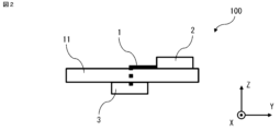
- FIG. 2 is a schematic diagram showing an outline of an antenna device 100 using the multilayer substrate 11 according to embodiment 1.
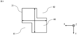
- FIG. 3 is a cross-sectional view showing an outline of a waveguide 31 of the multilayer substrate 11, and is a diagram showing the shape of a cross section perpendicular to the direction in which the waveguide 31 penetrates.
- FIG. 4 is a cross-sectional view showing an outline of another waveguide 31 of the multilayer substrate 11, and is a diagram showing the shape of a cross section perpendicular to the direction in which the waveguide 31 penetrates.
- FIG. 1 is a cross-sectional view showing an outline of a multilayer substrate 11 according to embodiment 1, and is a diagram of the multilayer substrate 11 cut at the A-A cross section position in FIG. 6.
- FIG. 2 is a schematic diagram showing an outline
- FIG. 5 is a cross-sectional view showing an outline of another waveguide 32 of the multilayer substrate 11, and is a diagram showing the shape of a cross section perpendicular to the direction in which the waveguide 32 penetrates.
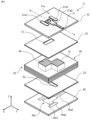
- FIG. 6 is an exploded perspective view showing an outline of the multilayer substrate 11.
- FIG. 7 is a diagram explaining the operation of the waveguide 31 of the multilayer substrate 11.
- FIG. 8 is a diagram showing the transmission line characteristics in the waveguide 31 of the multilayer substrate 11, and is a diagram showing the results of an electromagnetic field analysis of the reflection coefficient.
- the X-axis, Y-axis, and Z-axis shown in the figure are three axes perpendicular to each other.
- the direction parallel to the Y-axis is the first direction
- the direction parallel to the X-axis is the second direction
- the direction parallel to the Z-axis is the third direction, the Z-axis.
- the direction indicated by the arrow in the figure in the X-axis direction is the positive X-direction
- the direction opposite to the positive X-direction is the negative X-direction.
- the antenna device 100 includes a multi-layer substrate 11, a high-frequency signal generator 2, and an antenna 3.
- the multi-layer substrate 11 includes a feeder line 1 that propagates a signal from the high-frequency signal generator 2 to the antenna 3.
- the antenna device 100 using the feeder line 1 is a device that transmits high-frequency signals in the microwave band or millimeter wave band.
- Microwaves have a wavelength of 1 mm to 1 m and a frequency of 300 MHz to 300 GHz.
- Millimeter waves have a wavelength of 1 mm to 10 mm and a frequency of 30 GHz to 300 GHz.
- the antenna device 100 propagates a signal from a first direction to a second direction.
- the high frequency signal generator 2 that generates a high frequency signal is provided, for example, as an IC (Integrated Circuit).
- the power supply line 1 connects the high frequency signal generator 2 and the antenna 3.
- the high frequency signal generator 2 is arranged on the multi-layer board 11, and the antenna 3 is connected to the multi-layer board 11.
- the high frequency signal generator 2 is mounted on a surface of the multi-layer board 11 different from the board surface to which the antenna 3 is connected.
- the antenna 3 is connected to a first conductor layer or a fourth conductor layer, which will be described later.
- the first conductor layer is provided, for example, on one board surface of the multi-layer board 11, and the fourth conductor layer is provided on the other board surface of the multi-layer board 11.
- the high frequency signal generator 2 When the antenna 3 is connected to the first conductor layer, the high frequency signal generator 2 is arranged on the side of the fourth conductor layer, and when the antenna 3 is connected to the fourth conductor layer, the high frequency signal generator 2 is arranged on the side of the first conductor layer.
- the multilayer substrate 11 includes a first dielectric layer 41 having a first conductor layer 21 on one side and a second conductor layer 22 on the other side opposite to the one side, a second dielectric layer 42 having a third conductor layer 23 on one side and a fourth conductor layer 24 on the other side opposite to the one side, in which the third conductor layer 23 is disposed at a distance from the second conductor layer 22, one or more intermediate dielectric layers 43 disposed between the second conductor layer 22 and the third conductor layer 23, and a waveguide 31.
- the intermediate dielectric layer 43 may be either single or multiple.
- the multilayer substrate 11 includes five intermediate dielectric layers 43, which are intermediate dielectric layers 43a, 43b, 43c, 43d, and 43e.
- intermediate conductor layers 25 are provided between the respective intermediate dielectric layers 43.
- four intermediate conductor layers 25a, 25b, 25c, and 25d are provided.
- Each of the conductor layers of the multilayer substrate 11 is, for example, copper foil.
- the first dielectric layer 41, the second dielectric layer 42, and the intermediate dielectric layer 43 are stacked in the Z direction, and the surfaces on which each plate-like layer is stacked are parallel to the X direction and the Y direction.
- the waveguide 31 is a conductive cylindrical member that abuts against the inner circumferential surface of a through hole that penetrates a specific portion of the intermediate dielectric layer 43 in the direction from the second conductor layer 22 to the third conductor layer 23, and the inside of the cylindrical member is filled with a dielectric 44 made of a material different from the first dielectric layer 41, the second dielectric layer 42, and the intermediate dielectric layer 43.
- the material of the first dielectric layer 41, the second dielectric layer 42, and the intermediate dielectric layer 43 is, for example, a glass cloth-based epoxy resin.
- the material of the dielectric 44 filled in the waveguide 31 is, for example, an epoxy resin.
- a low-loss dielectric 44 can be provided on the inside of the waveguide 31.
- the performance of the waveguide 31 can be improved.
- the first conductor pattern 21a is formed on the first conductor layer 21.
- the fourth conductor pattern 24a is formed on the fourth conductor layer 24.
- the power supply line 1 is formed from the first conductor pattern 21a, the fourth conductor pattern 24a, and the waveguide 31.
- the shape of the first conductor pattern 21a in this embodiment will be described.
- the first conductor pattern 21a has a ring-shaped line portion 21a1 having a rectangular opening, and an input/output terminal portion 21a2 extending from the ring-shaped line portion 21a1 in the positive Y direction.
- the shape of the opening is not limited to a rectangle, and may be, for example, a polygon other than a rectangle.
- the input/output terminal portion 21a2 has a multi-step shape whose width changes between the ring-shaped line portion 21a1 and the end of the first dielectric layer 41.
- the first conductor pattern 21a has non-connected portions 21a3 on both sides in the X direction adjacent to the annular line portion 21a1, with a gap between them.
- the shape of the non-connected portions 21a3 is rectangular, but the shape of the non-connected portions 21a3 is not limited to a rectangle and may be, for example, a polygon other than a rectangle.
- the shape of the fourth conductor pattern 24a is the same as that of the first conductor pattern 21a.
- the fourth conductor pattern 24a has a ring-shaped line portion 24a1, an input/output terminal portion 24a2, and a non-connected portion 24a3.
- the extension direction of the input/output terminal portion 24a2 is different from the extension direction of the input/output terminal portion 21a2, and the extension direction of the input/output terminal portion 24a2 is the negative X direction.
- the antenna 3 is connected to an end of the input/output terminal portion 21a2 or the input/output terminal portion 24a2.
- the first conductor pattern 21a is electromagnetically coupled to the second slot 51.
- the opening of the annular line portion 21a1 is arranged to overlap with the second slot 51 when viewed in the Z direction, as shown in FIG. 1.
- the fourth conductor pattern 24a is electromagnetically coupled to the third slot 52.
- the opening of the annular line portion 24a1 is arranged to overlap with the third slot 52 when viewed in the Z direction.
- the shapes of the conductor patterns are not limited to the shapes shown in this embodiment, as long as each conductor pattern has a shape that electromagnetically couples with its respective slot.
- the second conductor layer 22 is formed with a second slot 51, which is an open portion of the second conductor layer 22, as shown in FIG. 6.
- the third conductor layer 23 is formed with a third slot 52, which is an open portion of the third conductor layer 23.
- the second slot 51 is electromagnetically coupled to the first conductor pattern 21a and the waveguide 31. When viewed in the Z direction, the second slot 51 is arranged so as to overlap with the first conductor pattern 21a and the inner portion of the waveguide 31, as shown in FIG. 1.
- the third slot 52 is electromagnetically coupled to the fourth conductor pattern 24a and the waveguide 31. When viewed in the Z direction, the third slot 52 is arranged so as to overlap with the fourth conductor pattern 24a and the inner portion of the waveguide 31.
- the second slot 51 and the third slot 52 are formed in a rectangular shape.
- each slot has a shape that electromagnetically couples with the respective conductor pattern and the waveguide 31, the shape of the slot is not limited to the shape shown in this embodiment.
- the slot may be a polygon other than a square or rectangle, or may have a floating conductor pattern in the inner region of the slot.
- ⁇ Waveguide 31> The configuration of the waveguide 31, which is a main part of the present application, will be described.
- the shape of the cross section of the waveguide 31 perpendicular to the direction of penetration through the intermediate dielectric layer 43 is a rectangle with both corners on one diagonal line cut out.
- the cut-out parts are called cut-out parts 61 and 62.
- the shape of the cut-out parts of the cross section of the waveguide 31 perpendicular to the direction of penetration through the intermediate dielectric layer 43 shown in FIG. 3 is a rectangle.
- the cut-out parts 61 and 62 may be square or rectangular as shown in FIG. 4.
- the cut-out parts 61 and 62 are arranged symmetrically with respect to the diagonal line opposite to the diagonal line where the cut-outs are provided.
- the cross-sectional quadrangle of the waveguide 31 is a square and the cutouts 61 and 62 are rectangular, the cutouts 61 and 62 are arranged asymmetrically with respect to the diagonal line opposite to the diagonal line where the cutouts are provided.
- the shape of the waveguide 31 can be easily designed according to the matching conditions of the transmission line characteristics propagating through the waveguide 31, because the shape of the cutout is simple.
- the shape of the cutout is not limited to a rectangle, and can be, for example, a polygon other than a rectangle, or a cutout shape that is asymmetrical, according to the matching conditions of the transmission line characteristics.
- the shape of the cutout is other than a rectangle, the number of design parameters increases, making it possible to design a waveguide 31 with more precise transmission characteristics.
- the corners of the rectangular cross section of the waveguide 31 are right angles or rounded.
- the corners of the rectangular cross section of the waveguide 31 shown in FIG. 3 of this embodiment are right angles. When the corners are right angles, the desired transmission characteristics can be easily obtained in the waveguide 31.
- the corners of the rectangular cross section of the waveguide 31 are not limited to right angles.
- the corners of the rectangular cross section of the waveguide 31 may be rounded depending on, for example, the manufacturing conditions of the waveguide 32 or the matching conditions of the transmission line characteristics.
- the other waveguide 32 has cutouts 63 and 64. When the corners are rounded, the manufacturability of the waveguide 32 is improved, and the productivity of the multilayer board 11 can be improved.
- FIG. 7(a) to 7(c) The operation of the waveguide 31 with the cutouts 61, 62 will be explained using Figures 7(a) to 7(c).
- the arrows shown in Figures 7(a) to 7(c) indicate the direction of the electric field excited in the second slot 51, the waveguide 31, and the third slot 52, respectively.
- the signal propagates in the negative Y direction of the first conductor pattern 21a, and then propagates in the negative X direction of the fourth conductor pattern 24a via the waveguide 31.
- the location where the electric field is excited is shown by a solid line
- the location where the electric field is excited thereafter is shown by a dashed line
- other locations are shown by dotted lines.
- the signal propagating in the negative Y direction of the first conductor pattern 21a is electromagnetically coupled to the second slot 51 as shown in FIG. 7(a), and an electric field is excited in the second slot 51 in the negative Y direction (perpendicular to the X axis).
- the signal electromagnetically coupled to the second slot 51 propagates through the waveguide 31 as shown in FIG. 7(b).
- the signal propagating through the waveguide 31 propagates while rotating 45 degrees with respect to the X axis according to the shape of the waveguide 31. Then, the signal rotated 45 degrees with respect to the X axis direction is electromagnetically coupled to the third slot 52 as shown in FIG. 7(c).
- the signal electromagnetically coupled to the third slot 52 propagates while further rotating 45 degrees with respect to the X axis according to the opening shape of the third slot 52.
- the electric field direction of the signal propagating through the third slot 52 is rotated 90 degrees with respect to the electric field direction of the signal propagating through the second slot 51, and finally, it is electromagnetically coupled to the fourth conductor pattern 24a and propagates in the negative X direction.
- the shape of the cross section perpendicular to the direction of penetrating the intermediate dielectric layer 43 in the waveguide 31 is a shape in which both corners on one diagonal line of a rectangle are cut out, so that the signal propagation direction can be changed by 90 degrees inside the multilayer substrate 11. Since the signal propagation direction can be changed by 90 degrees inside the multilayer substrate 11, an additional conductor pattern for changing the signal propagation direction is not required in either the first conductor layer 21 in which the first conductor pattern 21a is provided or the fourth conductor layer 24 in which the fourth conductor pattern 24a is provided. Since an additional conductor pattern is not required, the multilayer substrate 11 can be made smaller.
- the design freedom of the multilayer substrate 11 can be improved. Furthermore, since no discontinuity that abruptly changes the signal propagation direction occurs, the amount of unnecessary radiation can be suppressed. Furthermore, by using such a multilayer substrate 11 in the antenna device 100, the amount of unnecessary radiation can be suppressed, and an antenna device 100 that is smaller in size and has improved design freedom can be obtained.
- FIG. 8 is a diagram showing the reflection coefficient versus normalized frequency obtained by electromagnetic field analysis, with the horizontal axis representing normalized frequency and the vertical axis representing reflection coefficient.
- the reflection coefficient is -20 dB or less at a bandwidth of 8% or more, with the normalized frequency "1" at the center, and that good characteristics are realized.
- This characteristic means that the transmitted frequency propagates without reflection, and the structure of the waveguide 31 disclosed in this application makes it possible to change the signal propagation direction by 90 degrees with good characteristics.
- FIG. 8 shows the analysis results for the waveguide 31 having the vertical cross section shown in FIG. 3, the effectiveness of the structure of the waveguide 31 is the same for the other shapes of the waveguide 31 shown in embodiment 1 and other embodiments described later.
- the dimensions of the waveguide 31 will be described.
- the length of the intermediate dielectric layer 43 in the penetrating direction of the waveguide 31 is a quarter wavelength of the wavelength of the signal propagating through the waveguide 31.
- the direction of the signal propagating through the waveguide 31 is the plus Z direction or the minus Z direction.
- the wavelength of the signal propagating through the waveguide 31 is not limited to a quarter wavelength of the wavelength of the signal propagating through the waveguide 31, and may be changed according to preferred transmission line characteristics or design specifications.
- the length of the intermediate dielectric layer 43 in the penetrating direction of the waveguide 31 is a quarter wavelength of the wavelength of the signal propagating through the waveguide 31, the desired transmission characteristics can be easily obtained in the waveguide 31.
- the guide wavelength is calculated to be 2.25 mm.
- the length of a quarter of the guide wavelength is 0.56 mm.
- the waveguide 31 is provided in the multilayer substrate 11 so that the length of the waveguide 31 in the penetration direction in the intermediate dielectric layer 43 is 0.56 mm. If the length of the waveguide 31 in the penetration direction is 0.56 mm, the thickness of the multilayer substrate 11 is, for example, 1.1 mm.
- the distance between the opposing sides of the rectangular cross section of the waveguide 31 is half the wavelength of the signal propagating through the waveguide 31.
- the distance between the opposing sides of the rectangular cross section of the waveguide 31 is the distance indicated by the arrow.
- the distance between the opposing sides of the rectangular cross section of the waveguide 31 is not limited to half the wavelength of the signal propagating through the waveguide 31, and the length may be changed depending on the preferred transmission line characteristics or design specifications.
- the distance between the opposing sides of the rectangular cross section of the waveguide 31 is half the wavelength of the signal propagating through the waveguide 31, the desired transmission characteristics can be easily obtained in the waveguide 31.
- ⁇ Formation of Waveguide 31> An example of a method for forming the waveguide 31 will be described with reference to the waveguide 31 shown in FIG. 1.
- a through hole penetrating a specific portion of the intermediate dielectric layer 43 is formed by a drill.
- the inner circumferential surface of the through hole is plated to form a conductive tubular member.
- the plating material is, for example, copper.
- the conductive tubular member and the intermediate conductor layer 25 are electrically connected.
- the inside of the tubular member is filled with a dielectric 44 made of a material different from the first dielectric layer 41, the second dielectric layer 42, and the intermediate dielectric layer 43.
- the material of the dielectric 44 to be filled is, for example, epoxy resin.
- the waveguide 31 portion of the multilayer substrate 11 is formed.
- the second conductor layer 22, the third conductor layer 23, the first dielectric layer 41, the second dielectric layer 42, the first conductor layer 21, and the fourth conductor layer 24 are stacked and provided.
- a first conductor pattern 21 a is provided on the first conductor layer 21
- a fourth conductor pattern 24 a is provided on the fourth conductor layer 24 , thereby forming the multilayer substrate 11 .
- the multilayer substrate 11 comprises a first dielectric layer 41 having a first conductor layer 21 on one side and a second conductor layer 22 on the other side, a second dielectric layer 42 having a third conductor layer 23 on one side and a fourth conductor layer 24 on the other side, in which the third conductor layer 23 is disposed at a distance from the second conductor layer 22, one or more intermediate dielectric layers 43 disposed between the second conductor layer 22 and the third conductor layer 23, and a conductive tubular member abutting against the inner circumferential surface of a through hole penetrating a specific portion of the intermediate dielectric layer 43, and a conductive tubular member disposed on the inside of the tubular member.
- the waveguide 31 is filled with a dielectric 44 made of a material different from the first dielectric layer 41, the second dielectric layer 42, and the intermediate dielectric layer 43.
- the cross-sectional shape of the waveguide 31 perpendicular to the direction of penetration through the intermediate dielectric layer 43 is a rectangle with both corners on one diagonal line cut out, so that the signal propagation direction can be changed by 90 degrees inside the multilayer substrate 11, and therefore an additional conductor pattern for changing the signal propagation direction in either the first conductor layer 21 or the fourth conductor layer 24 is not required. Since an additional conductor pattern is not required, the multilayer substrate 11 can be made smaller. Furthermore, since an additional conductor pattern is not required and the area of the circuit does not increase, the design freedom of the multilayer substrate 11 can be improved. Furthermore, since no discontinuity that abruptly changes the signal propagation direction occurs, the amount of unnecessary radiation in the multilayer substrate 11 can be suppressed.
- the length of the intermediate dielectric layer 43 in the direction through which the waveguide 31 penetrates is a quarter of the wavelength of the signal propagating through the waveguide 31, the desired transmission characteristics can be easily obtained in the waveguide 31. Also, if the distance between opposing sides of the rectangular cross section of the waveguide 31 is a half of the wavelength of the signal propagating through the waveguide 31, the desired transmission characteristics can be easily obtained in the waveguide 31.
- the desired transmission characteristics can be easily obtained in the waveguide 31. If the corners of the rectangular cross section of the waveguide 31 are rounded, the desired transmission characteristics can be easily obtained and the manufacturability of the waveguide 31 is improved, thereby improving the productivity of the multilayer board 11.
- the shape of the cutout portion of the waveguide 31 in a cross section perpendicular to the direction of penetration through the intermediate dielectric layer 43 is rectangular, the shape of the cutout is simple, so the shape of the waveguide 31 can be easily designed according to the matching conditions of the transmission line characteristics propagating through the waveguide 31. Furthermore, when the shape of the cutout portions 61, 62 is other than rectangular, the number of design parameters increases, making it possible to design a waveguide 31 with more precise transmission characteristics.
- the antenna device 100 includes the multilayer substrate 11 disclosed in the present application and the antenna 3 connected to the first conductor layer 21 or the fourth conductor layer 24, the use of the multilayer substrate 11 disclosed in the present application in the antenna device 100 makes it possible to obtain an antenna device 100 that is smaller in size and has improved design freedom while suppressing the amount of unwanted radiation.
- FIG. 9 is a cross-sectional view showing an outline of the multilayer substrate 12 according to the second embodiment, and shows the multilayer substrate 12 cut at the same position as the A-A cross-sectional position in Fig. 6.
- Fig. 10 is a cross-sectional view of the multilayer substrate 12 cut at the B-B cross-sectional position in Fig. 9, showing a cross-sectional view of the intermediate dielectric layer 43c.
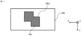
- Fig. 11 is a cross-sectional view of the multilayer substrate 12 cut at the C-C cross-sectional position in Fig. 9, showing a cross-sectional view of the intermediate conductor layer 25b.
- the multilayer substrate 12 according to the second embodiment has a configuration in which a waveguide 33 is formed by a plurality of via holes 71.
- the multilayer substrate 11 includes a first dielectric layer 41 having a first conductor layer 21 on one side and a second conductor layer 22 on the other side opposite the first side, a second dielectric layer 42 having a third conductor layer 23 on one side and a fourth conductor layer 24 on the other side opposite the first side, in which the third conductor layer 23 is disposed at a distance from the second conductor layer 22, one or more intermediate dielectric layers 43 disposed between the second conductor layer 22 and the third conductor layer 23, and a plurality of via holes 71 penetrating the intermediate dielectric layer 43 in the direction from the second conductor layer 22 to the third conductor layer 23 and surrounding a specific portion of the intermediate dielectric layer 43.
- the intermediate dielectric layer 43 may be single or multiple.
- the multilayer substrate 11 has five intermediate dielectric layers 43, that is, intermediate dielectric layers 43a, 43b, 43c, 43d, and 43e.
- intermediate conductor layers 25 are provided at least in the portions between the plurality of intermediate dielectric layers 43 excluding the waveguide 33 consisting of the plurality of via holes 71 and specific portions.
- four intermediate conductor layers 25a, 25b, 25c, and 25d are provided.
- Each of the conductor layers of the multilayer substrate 11 is, for example, copper foil.
- a waveguide 33 is formed by a plurality of via holes 71.
- the shape of the line connecting the plurality of via holes 71 in a cross section perpendicular to the direction of penetration of the intermediate dielectric layer 43 in the waveguide 33 is a shape in which both corners on one diagonal of a rectangle are cut out.
- the cut-out portions are called cut-out portions 65 and 66.
- the intermediate conductor layer 25b has an opening 25b1 surrounding a specific portion of the intermediate dielectric layer 43.
- the portion of the intermediate dielectric layer 43 shown in FIG. 11 is a portion of the intermediate dielectric layer 43c.
- the intermediate conductor layers 25a, 25c, and 25d have the same configuration as the intermediate conductor layer 25b.
- the plurality of via holes 71 are provided so as to overlap the periphery of the opening 25b1 surrounding the specific portion of the intermediate dielectric layer 43.
- the plurality of via holes 71 and the intermediate conductor layer 25 are electrically connected.
- the waveguide 33 is formed by 20 via holes 71, but the number of via holes 71 is not limited to this.
- the waveguide 33 formed by the multiple via holes 71 has a shape in which the line connecting the multiple via holes 71 in a vertical cross section has a shape in which both corners on one diagonal of a rectangle are cut out, so that the signal propagation direction can be changed by 90 degrees inside the multilayer substrate 12, similar to the waveguide 31 of the first embodiment. Since the signal propagation direction can be changed by 90 degrees inside the multilayer substrate 11, an additional conductor pattern for changing the signal propagation direction is not required in either the first conductor layer 21 on which the first conductor pattern 21a is provided or the fourth conductor layer 24 on which the fourth conductor pattern 24a is provided. Since an additional conductor pattern is not required, the multilayer substrate 12 can be made smaller. Furthermore, since an additional conductor pattern is not required and the area of the circuit does not increase, the design freedom of the multilayer substrate 12 can be improved. Furthermore, since no discontinuity that abruptly changes the signal propagation direction occurs, the amount of unnecessary radiation can be suppressed.
- the shape of the waveguide 31 depended on the size of the drill used to form the through holes, particularly in corners such as the corners of the waveguide 31.
- the waveguide 33 is formed by multiple via holes 71, so the shape of the waveguide 33 does not depend on the size of the drill, improving the design freedom for the shape of the waveguide 33.
- the multilayer substrate 12 includes a plurality of via holes 71 that penetrate the intermediate dielectric layer 43 in the direction from the second conductor layer 22 to the third conductor layer 23 and surround a specific portion of the intermediate dielectric layer 43, and the plurality of via holes 71 form a waveguide 33.
- the shape of the line connecting the plurality of via holes 71 in a cross section perpendicular to the direction of penetration of the intermediate dielectric layer 43 in the waveguide 33 is a shape in which both corners on one diagonal line of a rectangle are cut out, so that the signal propagation direction can be changed by 90 degrees inside the multilayer substrate 11, and therefore an additional conductor pattern for changing the signal propagation direction is not required in either the first conductor layer 21 or the fourth conductor layer 24.
- the waveguide 33 is formed by a plurality of via holes 71, the design freedom for the shape of the waveguide 33 can be improved. In addition, since no discontinuity that abruptly changes the signal propagation direction occurs, the amount of unnecessary radiation can be suppressed.
Landscapes
- Waveguides (AREA)
Priority Applications (3)
| Application Number | Priority Date | Filing Date | Title |
|---|---|---|---|
| PCT/JP2023/004374 WO2024166296A1 (ja) | 2023-02-09 | 2023-02-09 | 多層基板及びそれを用いたアンテナ装置 |
| JP2024575990A JP7699730B2 (ja) | 2023-02-09 | 2023-02-09 | 多層基板及びそれを用いたアンテナ装置 |
| US19/254,417 US20250329907A1 (en) | 2023-02-09 | 2025-06-30 | Multilayer substrate and antenna device using same |
Applications Claiming Priority (1)
| Application Number | Priority Date | Filing Date | Title |
|---|---|---|---|
| PCT/JP2023/004374 WO2024166296A1 (ja) | 2023-02-09 | 2023-02-09 | 多層基板及びそれを用いたアンテナ装置 |
Related Child Applications (1)
| Application Number | Title | Priority Date | Filing Date |
|---|---|---|---|
| US19/254,417 Continuation US20250329907A1 (en) | 2023-02-09 | 2025-06-30 | Multilayer substrate and antenna device using same |
Publications (1)
| Publication Number | Publication Date |
|---|---|
| WO2024166296A1 true WO2024166296A1 (ja) | 2024-08-15 |
Family
ID=92262171
Family Applications (1)
| Application Number | Title | Priority Date | Filing Date |
|---|---|---|---|
| PCT/JP2023/004374 Ceased WO2024166296A1 (ja) | 2023-02-09 | 2023-02-09 | 多層基板及びそれを用いたアンテナ装置 |
Country Status (3)
| Country | Link |
|---|---|
| US (1) | US20250329907A1 (https=) |
| JP (1) | JP7699730B2 (https=) |
| WO (1) | WO2024166296A1 (https=) |
Citations (5)
| Publication number | Priority date | Publication date | Assignee | Title |
|---|---|---|---|---|
| WO2005034278A1 (ja) * | 2003-10-06 | 2005-04-14 | Murata Manufacturing Co., Ltd. | ツイスト導波管および無線装置 |
| WO2010106198A1 (es) * | 2009-03-18 | 2010-09-23 | Radiacion Y Microondas, S.A. | Girador de polarización con múltiples secciones en forma de pajarita |
| JP2017005639A (ja) * | 2015-06-16 | 2017-01-05 | 日本電気株式会社 | 導波管取付装置 |
| JP2020202248A (ja) * | 2019-06-07 | 2020-12-17 | イビデン株式会社 | 配線基板及び配線基板の製造方法 |
| WO2022024318A1 (ja) * | 2020-07-30 | 2022-02-03 | 三菱電機株式会社 | 導波管カプラ |
Family Cites Families (2)
| Publication number | Priority date | Publication date | Assignee | Title |
|---|---|---|---|---|
| JP5990828B2 (ja) | 2010-03-09 | 2016-09-14 | 日立化成株式会社 | 電磁結合構造、多層伝送線路板、電磁結合構造の製造方法、及び多層伝送線路板の製造方法 |
| JP7144287B2 (ja) | 2018-05-11 | 2022-09-29 | 株式会社Soken | 層間伝送線路 |
-
2023
- 2023-02-09 WO PCT/JP2023/004374 patent/WO2024166296A1/ja not_active Ceased
- 2023-02-09 JP JP2024575990A patent/JP7699730B2/ja active Active
-
2025
- 2025-06-30 US US19/254,417 patent/US20250329907A1/en active Pending
Patent Citations (5)
| Publication number | Priority date | Publication date | Assignee | Title |
|---|---|---|---|---|
| WO2005034278A1 (ja) * | 2003-10-06 | 2005-04-14 | Murata Manufacturing Co., Ltd. | ツイスト導波管および無線装置 |
| WO2010106198A1 (es) * | 2009-03-18 | 2010-09-23 | Radiacion Y Microondas, S.A. | Girador de polarización con múltiples secciones en forma de pajarita |
| JP2017005639A (ja) * | 2015-06-16 | 2017-01-05 | 日本電気株式会社 | 導波管取付装置 |
| JP2020202248A (ja) * | 2019-06-07 | 2020-12-17 | イビデン株式会社 | 配線基板及び配線基板の製造方法 |
| WO2022024318A1 (ja) * | 2020-07-30 | 2022-02-03 | 三菱電機株式会社 | 導波管カプラ |
Also Published As
| Publication number | Publication date |
|---|---|
| JP7699730B2 (ja) | 2025-06-27 |
| US20250329907A1 (en) | 2025-10-23 |
| JPWO2024166296A1 (https=) | 2024-08-15 |
Similar Documents
| Publication | Publication Date | Title |
|---|---|---|
| JP5072968B2 (ja) | 導波管の接続構造 | |
| CN102414920B (zh) | 结构体、印刷板、天线、传输线波导转换器、阵列天线和电子装置 | |
| JP7692941B2 (ja) | メタサーフェスを有する多層導波管、アレンジメント、およびその製造方法 | |
| US7154441B2 (en) | Device for transmitting or emitting high-frequency waves | |
| JP2004153367A (ja) | 高周波モジュール、ならびにモード変換構造および方法 | |
| JP5566169B2 (ja) | アンテナ装置 | |
| US9629282B2 (en) | Electronic device, structure, and heat sink | |
| KR20150125262A (ko) | 다층 기판 및 다층 기판의 제조 방법 | |
| JP2005051331A (ja) | マイクロストリップ線路と誘電体導波管との結合構造 | |
| JP2007158675A (ja) | 多層プリント回路基板のビア構造、それを有する帯域阻止フィルタ | |
| US12451576B2 (en) | Double-sided board, radar apparatus, transmission member, and method of manufacturing transmission member | |
| JP3891996B2 (ja) | 導波管型導波路および高周波モジュール | |
| JP7702696B2 (ja) | 導波路 | |
| CN114128037A (zh) | 耦合部件、微波器件及电子设备 | |
| JP7699730B2 (ja) | 多層基板及びそれを用いたアンテナ装置 | |
| CN109950688B (zh) | 微带型isgw圆极化缝隙行波天线 | |
| JP7661469B2 (ja) | 印刷配線板 | |
| US12482913B2 (en) | Printed wiring board, multilayer resonator, and multilayer filter | |
| CN118104067A (zh) | 用于发送/接收数据的集成印刷电路板的天线 | |
| JP2000100993A (ja) | 高周波回路基板 | |
| CN109950694B (zh) | 带脊的isgw圆极化缝隙行波天线 | |
| JP7317244B2 (ja) | 給電線路及びそれを用いたアンテナ装置 | |
| JP7286726B2 (ja) | 伝送線路変換構造造、その調整方法、及びその製造方法 | |
| CN116156737B (zh) | 信号能量耦合传输的多层微波电路板以及电子电路 | |
| CN114122695B (zh) | 天线装置 |
Legal Events
| Date | Code | Title | Description |
|---|---|---|---|
| 121 | Ep: the epo has been informed by wipo that ep was designated in this application |
Ref document number: 23921127 Country of ref document: EP Kind code of ref document: A1 |
|
| WWE | Wipo information: entry into national phase |
Ref document number: 2024575990 Country of ref document: JP |
|
| NENP | Non-entry into the national phase |
Ref country code: DE |
|
| 122 | Ep: pct application non-entry in european phase |
Ref document number: 23921127 Country of ref document: EP Kind code of ref document: A1 |