WO2024162270A1 - ダイオード、これを用いた整流回路、及び受電レクテナ - Google Patents
ダイオード、これを用いた整流回路、及び受電レクテナ Download PDFInfo
- Publication number
- WO2024162270A1 WO2024162270A1 PCT/JP2024/002688 JP2024002688W WO2024162270A1 WO 2024162270 A1 WO2024162270 A1 WO 2024162270A1 JP 2024002688 W JP2024002688 W JP 2024002688W WO 2024162270 A1 WO2024162270 A1 WO 2024162270A1
- Authority
- WO
- WIPO (PCT)
- Prior art keywords
- electrode
- semiconductor layer
- diode
- cathode electrode
- connection portion
- Prior art date
- Legal status (The legal status is an assumption and is not a legal conclusion. Google has not performed a legal analysis and makes no representation as to the accuracy of the status listed.)
- Ceased
Links
Images







Classifications
-
- H—ELECTRICITY
- H10—SEMICONDUCTOR DEVICES; ELECTRIC SOLID-STATE DEVICES NOT OTHERWISE PROVIDED FOR
- H10D—INORGANIC ELECTRIC SEMICONDUCTOR DEVICES
- H10D8/00—Diodes
-
- H—ELECTRICITY
- H10—SEMICONDUCTOR DEVICES; ELECTRIC SOLID-STATE DEVICES NOT OTHERWISE PROVIDED FOR
- H10D—INORGANIC ELECTRIC SEMICONDUCTOR DEVICES
- H10D64/00—Electrodes of devices having potential barriers
- H10D64/60—Electrodes characterised by their materials
- H10D64/64—Electrodes comprising a Schottky barrier to a semiconductor
-
- H—ELECTRICITY
- H10—SEMICONDUCTOR DEVICES; ELECTRIC SOLID-STATE DEVICES NOT OTHERWISE PROVIDED FOR
- H10D—INORGANIC ELECTRIC SEMICONDUCTOR DEVICES
- H10D8/00—Diodes
- H10D8/50—PIN diodes
-
- H—ELECTRICITY
- H10—SEMICONDUCTOR DEVICES; ELECTRIC SOLID-STATE DEVICES NOT OTHERWISE PROVIDED FOR
- H10D—INORGANIC ELECTRIC SEMICONDUCTOR DEVICES
- H10D8/00—Diodes
- H10D8/60—Schottky-barrier diodes
-
- H—ELECTRICITY
- H10—SEMICONDUCTOR DEVICES; ELECTRIC SOLID-STATE DEVICES NOT OTHERWISE PROVIDED FOR
- H10W—GENERIC PACKAGES, INTERCONNECTIONS, CONNECTORS OR OTHER CONSTRUCTIONAL DETAILS OF DEVICES COVERED BY CLASS H10
- H10W20/00—Interconnections in chips, wafers or substrates
- H10W20/01—Manufacture or treatment
-
- H—ELECTRICITY
- H10—SEMICONDUCTOR DEVICES; ELECTRIC SOLID-STATE DEVICES NOT OTHERWISE PROVIDED FOR
- H10W—GENERIC PACKAGES, INTERCONNECTIONS, CONNECTORS OR OTHER CONSTRUCTIONAL DETAILS OF DEVICES COVERED BY CLASS H10
- H10W20/00—Interconnections in chips, wafers or substrates
- H10W20/40—Interconnections external to wafers or substrates, e.g. back-end-of-line [BEOL] metallisations or vias connecting to gate electrodes
- H10W20/45—Interconnections external to wafers or substrates, e.g. back-end-of-line [BEOL] metallisations or vias connecting to gate electrodes characterised by their insulating parts
- H10W20/48—Insulating materials thereof
Definitions
- This disclosure relates to a diode, a rectifier circuit using the same, and a receiving rectenna.
- GaN gallium nitride
- Ga 2 O 3 gallium oxide
- Diodes using GaN-based semiconductors and having an anode electrode divided into many circular electrodes are known (see, for example, Patent Document 1).
- the purpose of this disclosure is to provide a diode that reduces the product of capacitance C and resistance R (hereinafter referred to as the "CR product"), which represents the time constant, as well as a rectifier circuit and a receiving rectenna that use the same.
- the diode comprises: A substrate; a first semiconductor layer provided on the substrate and including a first impurity at a first concentration; a second semiconductor layer provided on the first semiconductor layer and including a second impurity at a concentration lower than the first concentration; a first electrode provided on the first semiconductor layer and surrounding at least a portion of the second semiconductor layer; a second electrode provided on the second semiconductor layer; having The width of the first electrode is 1 to 6 times the propagation length L t [m] defined by the following formula (1).
- L t [m] ( ⁇ C [ ⁇ m 2 ]/R S [ ⁇ /sq]) 1/2 (1)
- ⁇ C is the contact resistivity between the first semiconductor layer and the first electrode
- R S is the sheet resistance of the first semiconductor layer.
- a diode with a reduced CR product, a rectifier circuit using this, and a receiving rectenna are realized.
- FIGS. 2A and 2B are schematic diagrams of a top view and a cross section of a diode according to an embodiment.
- 2 is a schematic cross-sectional view of an entire diode including a pad electrode and wiring.
- FIG. FIG. 2 is a diagram showing an example of a diode array on a substrate.
- 1 is a diagram showing a schematic diagram of the propagation length Lt , the contact resistivity ⁇ C , and the sheet resistance Rs . 1 is a scanning electron microscope image of a sample prepared for measurement.
- FIG. 1 is a diagram showing the relationship between the cathode electrode width and the electrical resistance and capacitance, and a linear approximation of the capacitance as a function of the cathode electrode width.
- FIG. 1 is a diagram showing the relationship between the cathode electrode width and the electrical resistance and capacitance, and a linear approximation of the capacitance as a function of the cathode electrode width.
- FIG. 11 is a diagram showing the relationship between the cathode electrode width and the CR product.
- FIG. 13 is a diagram showing the relationship between the cathode electrode width and the contact resistance R C.
- FIG. 13 is a diagram showing the relationship between the cathode electrode width and the CRC product.
- FIG. 13 is a diagram showing the relationship between the cathode electrode width normalized by the propagation length and the CRC product.
- FIG. 2 is a schematic top view showing an example of an arrangement of diodes according to an embodiment.
- FIG. 13 is a schematic top view showing an arrangement of diodes in a reference example.
- FIG. 2 is a schematic cross-sectional view showing an arrangement of diodes according to an embodiment.
- 1 is a scanning electron microscope image of the bridge structure on the anode side.
- FIG. 4 is a schematic diagram of a connection portion of a bridge wiring.
- 13A and 13B are diagrams illustrating the shape-maintaining effect of the connection portion of the bridge wiring.
- 1A to 1C are manufacturing process diagrams of bridge wiring.
- 1A to 1C are manufacturing process diagrams of bridge wiring.
- 1A to 1C are manufacturing process diagrams of bridge wiring.
- 1A to 1C are manufacturing process diagrams of bridge wiring.
- 1A to 1C are manufacturing process diagrams of bridge wiring.
- 1A to 1C are manufacturing process diagrams of bridge wiring.
- 1A to 1C are manufacturing process diagrams of bridge wiring.
- 1A to 1C are manufacturing process diagrams of bridge wiring.
- 1A to 1C are manufacturing process diagrams of bridge wiring.
- 1 is a schematic diagram of a receiving rectenna using a rectifier circuit to which a diode of an embodiment is applied.
- ⁇ Basic structure of a diode> 1 is a schematic diagram of a part of the upper surface of a diode 10 of an embodiment and a cross section taken along line II'.
- the diode 10 includes a first semiconductor layer 11 containing a first impurity at a first concentration, a second semiconductor layer 12 provided on the first semiconductor layer 11 and containing a second impurity at a concentration lower than the first concentration, a first electrode 21 provided on the first semiconductor layer 11 and surrounding at least a part of the second semiconductor layer 12, and a second electrode 22 provided on the second semiconductor layer 12.
- the width of the first electrode 21, which is the distance between the inner wall and the outer wall of the first electrode 21, is 1 to 6 times the propagation length L t [m] defined by the following formula (1). Note that this propagation length L t is defined when the shape of the electrode is rectangular.
- the first semiconductor layer 11 and the second semiconductor layer 12 may be formed of a III-V group compound semiconductor such as a GaN-based semiconductor, an InP-based semiconductor, or a GaAs-based semiconductor, Si, SiC, Ga 2 O 3 , Al 2 O 3 , or diamond. These compound semiconductor materials may be binary, ternary, or quaternary.
- the first semiconductor layer 11 and the second semiconductor layer 12 are preferably made of a GaN-based semiconductor, which is a nitride semiconductor. GaN-based semiconductors, SiC, Ga 2 O 3 , and Al 2 O 3 have a large band gap, so that they have a high electric field resistance.
- the shape of the first semiconductor layer 11 and the second semiconductor layer 12 in a top view may be a circle, an ellipse, or a polygon.
- the first impurity contained in the first semiconductor layer 11 and the second impurity contained in the second semiconductor layer 12 may be the same or different.
- the first impurity and the second impurity may be n-type impurities or p-type impurities.
- the first impurity and the second impurity are preferably n-type impurities. This allows the resistance of the first semiconductor layer 11 and the second semiconductor layer 12 to be reduced.
- the first impurity and the second impurity may be Si, Ge, or Mg.
- the first impurity and the second impurity may be Sn or Zn.
- the first impurity and the second impurity may be Si, Sn, S, Se, or Te.
- Si, SiC, and diamond are used, N, P, As, Sb, B, and Al may be used.
- the concentration of the first impurity in the first semiconductor layer 11 is higher than the concentration of the second impurity in the second semiconductor layer 12.
- the concentration of the first impurity may be more than 1 time and 200,000 times or less, preferably 5 times or more and 50 times or less, compared to the concentration of the second impurity.
- the concentration of the first impurity may be, for example, an impurity concentration of 1 ⁇ 10 24 m ⁇ 3 or more and 1 ⁇ 10 28 m ⁇ 3 or less, preferably 1 ⁇ 10 25 m ⁇ 3 or more and 1 ⁇ 10 27 m ⁇ 3 or less.
- the second semiconductor layer 12 contains the second impurity at a concentration lower than that of the first impurity in order to maintain the reverse breakdown voltage.
- the concentration of the second impurity is lower than the concentration of the first impurity, and may be, for example, an impurity concentration of 5 ⁇ 10 22 m ⁇ 3 or more and 5 ⁇ 10 24 m ⁇ 3 or less, preferably 1 ⁇ 10 23 m ⁇ 3 or more and 1 ⁇ 10 24 m ⁇ 3 or less.
- a second electrode 22 is provided on the second semiconductor layer 12 in contact with the second semiconductor layer 12.
- the second electrode 22 is formed of a metal capable of making Schottky contact with the second semiconductor layer 12, in which the concentration of the second impurity is lower than that of the first impurity.
- a metal material having a work function larger than that of the second semiconductor layer 12 is selected to form a Schottky barrier between the second electrode 22 and the second semiconductor layer 12.
- a metal material that forms a Schottky barrier of a desired size is used in relation to the material used for the second semiconductor layer 12. This provides a Schottky barrier diode that passes only the current flowing from the second electrode 22 toward the second semiconductor layer 12.
- a Schottky barrier may be formed between the second electrode 22 and the second semiconductor layer 12 by selecting a metal material having a work function smaller than that of the second semiconductor layer 12 as the second impurity.
- the second impurity is preferably an n-type impurity. This allows the electrical resistance of the second semiconductor layer 12 to be further reduced.
- the second electrode 22 of the Schottky barrier diode is also referred to as the "anode electrode 22" and the first electrode 21 is also referred to as the "cathode electrode 21".
- the second electrode 22 contains at least one selected from the group consisting of Ni, Pt, and Au.
- the planar shape of the second electrode 22 may be circular, elliptical, rectangular, or other polygonal.
- the cathode electrode 21 is formed of a metal material capable of making ohmic contact with the first semiconductor layer 11.
- the cathode electrode 21 includes at least one selected from the group consisting of Al, Ti, V, Pt, and Au. Since the first semiconductor layer 11 includes the first impurity at a high concentration, the work function of the metal material of the cathode electrode 21 does not necessarily need to be set lower than the work function of the first semiconductor layer 11.
- the cathode electrode 21 is formed of aluminum (Al) having low electrical resistance.
- the cathode electrode 21 may include a titanium (Ti) thin film that enhances the adhesion of the interface between the Al layer and the first semiconductor layer 11.
- the cathode electrode 21 may be multi-layered, and one layer may include multiple metals.
- the cathode electrode 21 is provided so as to surround at least a portion of the second semiconductor layer 12. In the example of FIG. 1, the cathode electrode 21 surrounds the entire circumference of the second semiconductor layer 12.
- the planar shape of the cathode electrode 21 may be partially open, such as a C-shape, but it is preferable to adopt a ring shape as shown in FIG. 1 in order to reduce current bias.
- the shape surrounded by the inner side surface and/or the shape surrounded by the outer side surface of the cathode electrode 21 may be a polygon such as a triangle or a rectangle, but it is preferable to adopt a circular ring shape as shown in FIG. 1 in order to prevent current concentration in the corners of the polygon.
- the planar shape of the cathode electrode 21 may be an ellipse.
- the planar shape of the cathode electrode 21 may be wider on the outside than on the center. For example, it may be a gourd shape.
- the distance between the inner wall and the outer wall of the cathode electrode 21 is defined as the first electrode width LE .
- This distance represents the distance between the inner wall and the outer wall in a direction perpendicular to the tangent of the inner wall of the cathode electrode 21 when viewed from above.
- the first electrode width LE is hereinafter also referred to as the cathode electrode width LE , or simply the width LE .
- the cathode electrode width LE is 1 to 6 times the propagation length Lt [m] defined by the above formula (1).
- the cathode electrode width LE is in the above range.
- the high frequency here includes the gigahertz band to the terahertz band, which are the frequency bands of wireless communication.
- the diode 10 of the embodiment has rectification characteristics in the range of, for example, 0.9 GHz to 500 GHz.
- the length of the inner wall of the portion where the first electrode width L E is 1 to 6 times the propagation length L t may be 70% or more, preferably 80% or more, and more preferably 90% or more of the entire length of the inner wall of the first electrode 21. This makes it possible to efficiently reduce the component of the CR product (representing the CR C product described later) derived from the first electrode 21.
- the diode 10 is configured by forming a first semiconductor layer 11 and a second semiconductor layer 12 on a substrate 5.
- the substrate 5 is an insulating substrate such as sapphire, or a semi-insulating substrate such as GaN, GaAs, or SiC to which no impurities are added.
- the first semiconductor layer 11 and the third semiconductor layer 13 are formed on the substrate 5.
- the third semiconductor layer 13 is formed in an area on the substrate 5 where the first semiconductor layer 11 is not provided, and contains the same impurity as the first semiconductor layer 11 at the same concentration.
- Both the first semiconductor layer 11 and the third semiconductor layer 13 may be n-type semiconductor layers in which the concentration of the first impurity is higher than that of the second semiconductor layer 12.
- the diode 10 has a pad electrode 31 disposed on the upper surface and side surface of the cathode electrode 21 on the first semiconductor layer 11.
- the pad electrode 31 contains at least gold (Au).
- the pad electrode 31 may have a nickel (Ni) thin film on the interface side with the cathode electrode 21.
- the pad electrode 31 overlaps the cathode electrode 21 containing Al.
- the cathode electrode 21 itself is an electrode having a width L E determined by the propagation length L t , and the area overlapping with the pad electrode 31 is small. Therefore, the diffusion of different metals, specifically the diffusion and mixing of Al and Au, is reduced.
- a pad electrode 32 is provided on the upper surface of the anode electrode 22.
- a pad electrode 33 is provided to cover the upper surface and side surface of the third semiconductor layer 13, and a pad electrode 34 is provided on the pad electrode 33.
- the pad electrodes 33 and 34 may be called "third electrodes”.
- a bridge wiring 35 is provided to electrically connect the anode electrode 22 to the pad electrodes 33 and 34 as the third electrodes. More specifically, the anode electrode 22 is connected to one end of the bridge wiring 35 via the pad electrode 32, and the third electrode including the pad electrode 33 and the pad electrode 34 is connected to the other end of the bridge wiring 35.
- the pad electrode 33 extends to an anode pad described later on the substrate 5, and the pad electrode 31 connected to the cathode electrode 21 extends to a cathode pad described later on the substrate 5.
- the pad electrode 34 may be omitted.
- the bridge wiring 35 is directly connected to the pad electrode 33.
- the width of the bridge wiring 35 may be, for example, 2 ⁇ m or more and 7 ⁇ m or less.
- the height of the bridge wiring 35 can be increased, thereby reducing the parasitic capacitance between the bridge wiring 35 and the electrode material in the lower layer.
- the width LE of the cathode electrode 21 determined by the propagation length Lt is set small within the above-mentioned range, the length of the bridge wiring 35 can be shortened, and the occurrence of breaks or shorts in the bridge wiring 35 and an increase in resistance can be reduced.
- FIG. 3 shows an example of a diode array on the substrate 5.
- a plurality of diodes may be connected in parallel.
- seven diodes 10 are connected in parallel.
- the cathode electrode 21 of each diode 10 is connected to the cathode pad 41, and the anode electrode 22 is connected to the anode pad 42 via the bridge wiring 35.
- the radius of the anode electrode 22 is r
- the width of the cathode electrode 21 is L E
- the distance between the anode electrode 22 and the cathode electrode 21 is d.
- the cathode electrode 21 with an inner diameter of 6 ⁇ m and a width L E is provided to surround the anode electrode 22 with a diameter of 4 ⁇ m.
- the capacitance C between the anode electrode 22 and the cathode electrode 21 is, for example, about 0.2 pF.
- Fig. 4 is a model of a distributed constant circuit when the shape of the electrode is assumed to be rectangular.
- Fig. 4 shows a schematic diagram of the propagation length Lt , contact resistivity ⁇ C , and sheet resistance Rs .
- the position in the width direction from the position P0 on the side of the cathode electrode closer to the anode is defined as x.
- the current flowing from the anode electrode to the cathode electrode at the position P0 is defined as I0
- the voltage is defined as V0 .
- the contact resistance Rc [ ⁇ ] at the position P0 is expressed as V0 / I0 .
- the contact resistance R C of the cathode electrode 21 is considered to be a ladder combination of minute sheet resistance R S ⁇ ds/W [ ⁇ ] in a direction parallel to the interface between the cathode electrode 21 and the first semiconductor layer 11 and minute contact resistivity ⁇ C /(dx ⁇ W) [ ⁇ ] in a direction perpendicular to the interface.
- the sheet resistance is the resistance of the first semiconductor layer 11 applied to a current flowing parallel to the interface.
- the contact resistivity is the contact resistance per unit area (1 m 2 ) when a current flows in a direction perpendicular to the interface.
- R C (R S ⁇ C ) 1/2 /W (4) where V(x) and I(x) are the voltage and current at position x.
- W is the thickness of the cathode electrode perpendicular to the width direction, and is a constant.
- a DC circuit is assumed, so capacitance and inductance are ignored.
- the differential equation is solved using the real parts of the distributed series impedance and distributed parallel admittance.
- the current I0 at the position P0 attenuates by the sheet resistance and the contact resistivity up to the position x while reaching the position x.
- the attenuation of the current I(x) is expressed by an exponential function as shown in FIG.
- the current I(x) is expressed by the following equation (5).
- ⁇ Measurement and evaluation of CR product> 5 is a scanning electron microscope (SEM) image of a sample prepared on a substrate 5 for measurement.
- the diameter of the anode electrode 22 is 4 ⁇ m
- the inner diameter of the cathode electrode 21 is 6 ⁇ m
- the distance d (see FIG. 3) from the circumference of the anode electrode 22 to the inner side surface of the cathode electrode 21 is 1 ⁇ m.
- Four types of samples were prepared by changing the design value of the radial width LE of the cathode electrode 21 to 3 ⁇ m, 6 ⁇ m, 10 ⁇ m, and 20 ⁇ m, and the capacitance C of each sample was measured with an LCR meter and the resistance R with a semiconductor parameter analyzer. Each sample is the result of four diodes connected in parallel.
- the graphs connected by solid lines in FIG. 6 show the relationship between the cathode electrode width L E [ ⁇ m] and the electrical resistance R [ ⁇ ] and capacitance C [pF].
- the graphs connecting the plots of black circles show the change in electrical resistance R
- the graphs connecting the plots of white circles show the change in capacitance C.
- the cathode electrode width L E increases, the capacitance C increases and the electrical resistance R decreases.
- the contact area between the cathode electrode and the first semiconductor layer 11 increases, so it was expected that the electrical resistance would decrease.
- the cathode electrode width L E does not contribute to an increase in capacitance, but in this experiment, the capacitance tends to increase as the cathode electrode width increases. Such an increase in capacitance was thought to be due to the fact that, for example, as the distance from the anode electrode increases in top view, a capacitance component that couples with the leakage component of the first semiconductor layer may occur.
- the result of the cathode electrode width L E of 3 ⁇ m is the result of a sample in which the cathode electrode is provided only on the first semiconductor layer 11.
- the results for the cathode electrode width LE of 6 ⁇ m, 10 ⁇ m, and 20 ⁇ m represent the average value of six samples produced.
- the CR product is plotted based on the measurement data in FIG.
- FIG. 7 shows the relationship between the cathode electrode width L E [ ⁇ m] and the CR product [pF ⁇ ].
- the cathode electrode width L E [ ⁇ m] that minimizes the CR product may vary depending on the design.
- the capacitance C is expressed as a formula. Based on the measurement results of FIG. 6, the capacitance C is obtained as a function of the cathode electrode width L E.
- Table 1 shows design examples in which the sheet resistance R S and contact resistivity ⁇ C were changed.
- the sheet resistance R S was set to two values, 11.11 [ ⁇ /sq] and 20 [ ⁇ /sq].
- the contact resistivity ⁇ C [ ⁇ m 2 ] is determined in four ways from the definition formula of the propagation length L t . Therefore, a total of eight design patterns A1, A2, B1, B2, C1, C2, D1, and D2 were set.
- R s and ⁇ c are quantities specific to the material and device conditions, so they do not depend on the shape of the electrode. Therefore, the values of the sheet resistance R s and contact resistivity ⁇ C assumed from the propagation length L t defined in the rectangular model can also be applied to the cylindrical model.
- the differential equations were solved numerically assuming a cylindrical electrode.
- a distributed parameter circuit model can usually be analytically solved assuming a rectangular electrode as explained in Figure 4, but a cylindrical electrode model cannot be analytically solved.
- the part corresponding to W in the differential equation explained in FIG. 4 is 2 ⁇ x.
- the values in Table 1 were used for Rs and ⁇ C .
- I(3 ⁇ ) and V(3 ⁇ ) were set as the initial conditions for I(x) and V(x).
- "3 ⁇ " is the distance from the center of the cylinder to the end of the inner wall of the cathode electrode, which is half the value of the inner diameter of 6 ⁇ m. The current spreads in the radial direction from this position. I(3 ⁇ ) was assumed to be 10 mA.
- V(3 ⁇ ) is the voltage used to calculate the contact resistance R C , and is corrected at the end as described later.
- V(3.02 ⁇ ) and I(3.02 ⁇ ) at x 3.02 ⁇ in the same way. Repeat this process up to the position of the outer wall of the cathode electrode. Note that dV(x)/dx and dI(x)/dx are quantities that change depending on the position x.
- V(3 ⁇ ) is an assumed value and needs to be corrected.
- the correction of V(3 ⁇ ) utilizes the boundary conditions. That is, the fact that the current does not flow in the radial direction at the end of the cathode electrode width is utilized.
- V(3 ⁇ ) is changed and the above calculation process is repeated to search for an initial value V(3 ⁇ ) that satisfies the boundary condition when the position x is the position of the outer wall of the electrode. If V(3 ⁇ ) that satisfies the boundary condition is obtained, the contact resistance R C can be obtained by calculating V(3 ⁇ )/I(3 ⁇ ). Note that V(3 ⁇ )/I(3 ⁇ ) does not depend on the initial value. Also, if the value of the current or electrical resistance at the position x where the boundary conditions are defined is within a range of ⁇ 10% of the set value, the calculation may be completed with that value. Since the result obtained by the calculation corresponds to one diode, if seven diodes are connected in parallel, this value can be divided by 7. In this way, the contact resistance R C of the diode when the number of parallel connections is seven can be obtained.
- FIG. 8 shows the relationship between the cathode electrode width L E and the contact resistance R C by numerical calculation.
- the contact resistance R C decreases.
- the design patterns A1, A2, B1, and B2 the smaller the value of the contact resistivity ⁇ C (see FIG. 8), the smaller the cathode electrode width L E is, the more the contact resistance R C saturates and the smaller the contact resistance R C is.
- the resistance of the diode 10 changes with the contact resistance R C.
- the CR product for convenience, called the "CR C product" of the capacitance C and the contact resistance R C of the cathode electrode changes.
- FIG. 9 shows the relationship between the cathode electrode width LE and the CRC product.
- the capacitance C uses the value of equation (4) obtained by linear approximation. From FIG. 9, it was predicted that the cathode electrode width LE at which the CRC product is minimized differs for each design. It is necessary to specify the optimal cathode electrode width LE regardless of the design, that is, the cathode electrode width LE at which the CRC product is minimized or a value close to the minimum.
- FIG. 10 shows the relationship between the cathode electrode width LE normalized by the propagation length Lt and the CR C product normalized by the CR c product when the normalized cathode electrode width LE is 1.
- the horizontal axis is the cathode electrode width LE normalized by the propagation length Lt
- the normalized CRc value can be 1 or less.
- the normalized CRc value can be 0.95 or less.
- the cathode electrode width LE is in the range of 1.8 ⁇ Lt or more and 4.2 ⁇ Lt or less, the normalized CRc value can be made 0.9 or less.
- the cathode electrode width LE is in the range of 2 ⁇ Lt or more and 4 ⁇ Lt or less, the normalized CRc value can be made 0.88 or less.
- the first electrode (cathode electrode) width is 1.5 times or more and 5 times or less, 1.8 times or more and 4.2 times or less, or 2 times or more and 4 times or less of the propagation length Lt. This makes it possible to reduce the CRC product. Therefore, it is possible to reduce the CR product.
- the width of the cathode electrode 21 of the diode 10 of the embodiment is set in the range of 1 to 6 times the propagation length Lt defined by the formula (1).
- the CRc product is kept at or near the minimum, and good rectification characteristics are obtained in the high frequency band, particularly in the range of 0.9 GHz to 500 GHz.
- the resistance value is large relative to the change in capacitance, and the CR product is unlikely to be a problem.
- the propagation length Lt used in the above description is a parameter that can be designed from the sheet resistance Rs and the contact resistivity ⁇ C obtained based on the TLM (Transmission Line Model) method.
- the sheet resistance Rs can be obtained by performing Hall measurement on the diode.
- the electrodes used for the Hall measurement are obtained by removing the electrodes provided on the diode and providing four new terminals.
- the contact resistivity ⁇ C can be roughly estimated from the slope of the IV characteristics.
- the range of the cathode electrode width LE can be determined for the range of the propagation length estimated from these values.
- the contact resistivity ⁇ C may be determined by measuring the dependency of the electrical resistance on the width of the cathode electrode.
- the width of the cathode electrode may be reduced using a focused ion beam or the like, and the contact resistivity ⁇ C may be determined from the electrical resistance at each width.
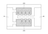
- Fig. 11A is a top schematic diagram showing an example of an arrangement of the diodes 10 of the embodiment.
- Fig. 11B is a schematic diagram of a configuration using a large-area common cathode electrode 210 in the same anode arrangement as Fig. 11A.
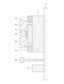
- Fig. 11C is a cross-sectional view of a state in which a pad electrode 31 is provided to cover the upper surface and side surface of the cathode electrode.
- Figs. 11A, 11B, and 11C are used to show the effect of reducing metal diffusion by the configuration of the cathode electrode 21 of the embodiment.
- the electrode material is selected so that the electrical resistance is small according to the material of the first semiconductor layer 11. However, the electrical resistance may increase due to diffusion or migration of the electrode material.
- the cathode electrode 21 or the common cathode electrode 210 is provided on the first semiconductor layer 11 on the substrate 5, and the pad electrode 31 is provided to cover the upper and side surfaces of the cathode electrode 21 or the common cathode electrode 210.
- the cathode electrode 21 and the common cathode electrode 210 are formed of the same material and the same thickness, but have different planar areas. In the models of FIG. 11A and FIG.
- both the cathode electrode 21 and the common cathode electrode 210 have a Ti layer with a thickness of 10 nm and an Al layer with a thickness of 300 nm on the Ti layer.
- the pad electrode 31 overlapping the cathode electrode 21 and the common cathode electrode 210 has a Ni layer with a thickness of 10 nm and an Au layer with a thickness of 500 nm on the Ni layer.
- the pad electrode 31 is connected to the cathode pad 41.
- the cathode electrode 21 of the embodiment is an electrode that individually surrounds each anode electrode 22, and the area of each cathode electrode 21 is smaller than that of the common cathode electrode 210, thereby reducing metal diffusion.
- FIG. 12 is an SEM image of the bridge structure on the anode side.
- the bridge wiring 35 has a first connection portion 351 connected to the anode electrode 22, a second connection portion 352 connected to the pad electrode 33, and a third connection portion 353 that connects between the first connection portion 351 and the second connection portion 352. More specifically, the first connection portion 351 of the bridge wiring 35 is connected to the anode electrode 22 via the pad electrode 32, and the second connection portion 352 is connected to the pad electrode 33 via the pad electrode 34.
- the cathode electrode 21 is provided surrounding the periphery of the anode electrode 22, and the pad electrode 31 overlaps the cathode electrode 21.
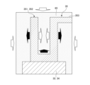
- the first connection part 351 and the second connection part 352 of the bridge wiring 35 have a cup-like shape with a recess, and each has a first opening 355 and a second opening 356.
- the third connection part 353 connects the edge 357 of the first opening 355 and the edge 358 of the second opening 356.
- the first connection portion 351 is formed by a first bottom 361 and a first side wall 363 surrounding the first bottom 361, and has a first opening 355 at the upper end of the first side wall 363.
- the second connection portion 352 is formed by a second bottom 362 and a second side wall 364 surrounding the second bottom 362, and has a second opening 356 at the upper end of the second side wall 364.
- the contribution of the skin effect becomes large in the frequency range of 20 GHz or more and 500 GHz or less.
- the skin effect is a phenomenon in which the current becomes more difficult to flow the further away from the surface of the conductor, and this phenomenon is more pronounced at higher frequencies. In such a thickness range, the skin effect can reduce the increase in electrical resistance when current flows from the inside and outside of the side wall.
- the third connection part 353 is connected to the first side wall 363, so that the current flows from the inside and outside of the first side wall 363.
- the surface area through which the high-frequency current flows increases.
- the current concentrates on the surface of the cylinder, and almost no current flows inside the conductor, resulting in high resistance.
- the first connection part 351 and the second connection part 352 of the bridge wiring 35 current flows in the area along the outer wall and the area along the inner wall, reducing resistance compared to a typical cylindrical conductor.
- the diode 10 of the embodiment can suppress metal diffusion between electrodes on the cathode side, and can reduce the resistance of the bridge wiring 35 on the anode side, thereby reducing deformation, breakage, and collapse of the bridge wiring 35.
- FIG. 15A shows a state immediately before the bridge wiring 35 is formed.
- the main part of the diode 10 is formed, including the cathode electrode 21 provided on the first semiconductor layer 11 and the anode electrode 22 provided on the second semiconductor layer 12.
- the cathode electrode 21 surrounds at least a part of the periphery of the second semiconductor layer 12, and has a ring-shaped or C-shaped planar shape.
- the radial width of the cathode electrode 21 is set to be 1 to 6 times the propagation length Lt described above, and the CR product is reduced.
- the third semiconductor layer 13 is formed in an area where the first semiconductor layer 11 is not provided.
- the first semiconductor layer 11 and the third semiconductor layer 13 are formed by etching a semiconductor layer grown by metalorganic chemical vapor deposition to separate it into two pieces, and the same impurity is injected into them.
- Each of the components in FIG. 15A can be formed by a known process.
- a negative resist 52 is applied to the substrate 5, the first semiconductor layer 11, the second semiconductor layer 12, the third semiconductor layer 13, the cathode electrode 21, and the anode electrode 22, and a mask is formed in the desired position by covering the necessary areas, exposing, and developing.
- a mask is formed in the desired position by covering the necessary areas, exposing, and developing.
- a pad electrode 31 is provided to cover the upper surface and side surface of the cathode electrode 21 and the side surface of the first semiconductor layer 11, and a pad electrode 33 is provided to cover the entire upper surface and side surface of the third semiconductor layer 13.
- the pad electrodes 31 and 33 can be formed in the same process.
- the exposed electrode surfaces are cleaned, and then a conductive layer for the pad electrode 31 is formed on the cathode surface, a conductive layer for the pad electrode 33 is formed on the surface of the third semiconductor layer 13, and a conductive layer for the pad electrode 32 is formed inside the aperture 53 by sputtering.
- the conductive layer for the pad electrode 32 has a film configuration in which, for example, Ti, platinum (Pt), and Au are laminated in this order.
- the resist 52 and the metal material attached to the resist 52 are removed by lift-off. This results in the pad electrode 32 that is connected to the anode electrode 22.
- a positive resist 56 is applied to the substrate 5, the first semiconductor layer 11, the second semiconductor layer 12, the third semiconductor layer 13, the cathode electrode 21, the anode electrode 22, and the pad electrodes 31, 32, and 33, and the necessary locations are exposed and developed to form apertures 57 and 58.
- the pad electrode 32 on the anode electrode 22 is exposed inside the aperture 57.
- a conductive film 59 is formed by sputtering on the upper surface of the positive resist 56 and inside the apertures 57 and 58.
- the conductive film 59 is, for example, an Au film.
- a first opening 355 and a second opening 356 are formed in the conductive film 59 on the pad electrode.
- a positive resist 61 is applied to the upper surface of the conductive film 59.
- the positive resist 61 is applied so as to fill the first opening 355 and the second opening 356.
- the area other than the area where the bridge wiring 35 is to be formed is exposed to light to form a resist mask 62.
- the diode 10 is covered with a protective film 65 such as polyimide.
- the first semiconductor layer 11, the second semiconductor layer 12, the third semiconductor layer 13, the cathode electrode 21, the anode electrode 22, the pad electrodes 31, 33, and the bridge wiring 35 are covered with the protective film 65.
- the protective film 65 is also filled inside the first opening 355 of the first connection portion 351 of the bridge wiring 35 and the second opening 356 of the second connection portion 352, so that the bridge wiring 35 is stably held.
- the protective film 65 is formed, for example, by a spin coating method.
- the above steps form the diode 10 of the embodiment.
- the diode 10 of the embodiment has a reduced CRC product at the cathode electrode 21, and therefore the CR product of the diode 10 is reduced, making it useful for applications such as high-frequency power transmission and energy harvesting.
- ⁇ Application examples of diodes> 16 is a schematic diagram of a receiving rectenna 70 to which the diode 10 of the embodiment is applied.
- the receiving rectenna 70 has a receiving antenna 71 and a rectifier circuit 72.
- the rectifier circuit 72 has the diode 10 of the embodiment.
- the receiving antenna 71 is capable of receiving electromagnetic waves of 0.9 GHz or more and 500 GHz or less.
- the electromagnetic waves received by the receiving antenna 71 are rectified by the rectifier circuit 72 and output as DC power.
- a stub line may be inserted on the input side of the rectifier circuit 72.
- the rectifier circuit also includes a capacitance. This capacitance smoothes the positive current that oscillates only in the positive direction. This converts AC power into DC power.
- the width of the cathode electrode 21 is set in the range of 1 to 6 times the propagation length Lt, the inner diameter of the cathode electrode 21, the diameter of the anode electrode 22, the distance between the anode electrode 22 and the cathode electrode 21, the impurity concentration of the second semiconductor layer 12, the voltage resistance characteristics, etc. can be appropriately designed.
- the materials of the pad electrodes 31, 32, 33, and 34 can also be selected appropriately.
- the cross-sectional shapes of the first connection part 351 and the second connection part 352 of the bridge wiring 35 are appropriately designed, such as a circle, an ellipse, or a polygon.
- the first connection part 351 and the second connection part 352 have a first opening 355 and a second opening 356 according to their cross-sectional shapes.
- the present disclosure described above may include the following configurations.
- (Item 1) A substrate; a first semiconductor layer provided on the substrate and including a first impurity at a first concentration; a second semiconductor layer provided on the first semiconductor layer and including a second impurity at a concentration lower than the first concentration; a first electrode provided on the first semiconductor layer and surrounding at least a portion of the second semiconductor layer; a second electrode provided on the second semiconductor layer; having The width of the first electrode is 1 to 6 times the propagation length L t [m] defined by the following formula (1): diode.
- the diode according to any one of items 1 to 4, comprising: (Item 6)
- the bridge wiring includes a first connection portion connected to the second electrode, a second connection portion connected to the third electrode, and a third connection portion connecting the first connection portion and the second connection portion.
- the company has the first connection portion has a first opening formed by a first bottom portion and a first sidewall surrounding the first bottom portion; the second connection portion has a second opening formed by a second bottom portion and a second sidewall surrounding the second bottom portion;
- the third connection portion connects an edge of the first opening and an edge of the second opening.
- Item 6 The diode according to item 5. (Item 7) a protective film that covers the first semiconductor layer, the second semiconductor layer, the third semiconductor layer, the first electrode, the second electrode, the third electrode, and the bridge wiring 35; 6.
- the diode according to item 5, comprising: (Item 8) Has rectification characteristics in the frequency range of 0.9 GHz to 500 GHz, Item 8.
- the material of the first semiconductor layer and the second semiconductor layer is a nitride semiconductor.
- Item 9 The diode according to any one of items 1 to 8.
- Item 10 a Schottky barrier between the second semiconductor layer and the second electrode;
- Item 10 The diode according to any one of items 1 to 9.
- Item 11 Item 11.
- a rectifier circuit comprising the diode according to any one of items 1 to 10.
- Item 12 A rectifier circuit according to claim 11; a receiving antenna connected to the rectifier circuit; A receiving rectenna having a receiving element.
Landscapes
- Electrodes Of Semiconductors (AREA)
Priority Applications (2)
| Application Number | Priority Date | Filing Date | Title |
|---|---|---|---|
| JP2024574894A JPWO2024162270A1 (https=) | 2023-01-31 | 2024-01-29 | |
| CN202480009524.9A CN120570083A (zh) | 2023-01-31 | 2024-01-29 | 二极管、使用二极管的整流电路及接收整流天线 |
Applications Claiming Priority (2)
| Application Number | Priority Date | Filing Date | Title |
|---|---|---|---|
| JP2023013629 | 2023-01-31 | ||
| JP2023-013629 | 2023-01-31 |
Publications (1)
| Publication Number | Publication Date |
|---|---|
| WO2024162270A1 true WO2024162270A1 (ja) | 2024-08-08 |
Family
ID=92147651
Family Applications (1)
| Application Number | Title | Priority Date | Filing Date |
|---|---|---|---|
| PCT/JP2024/002688 Ceased WO2024162270A1 (ja) | 2023-01-31 | 2024-01-29 | ダイオード、これを用いた整流回路、及び受電レクテナ |
Country Status (3)
| Country | Link |
|---|---|
| JP (1) | JPWO2024162270A1 (https=) |
| CN (1) | CN120570083A (https=) |
| WO (1) | WO2024162270A1 (https=) |
Citations (4)
| Publication number | Priority date | Publication date | Assignee | Title |
|---|---|---|---|---|
| JP2015041714A (ja) * | 2013-08-23 | 2015-03-02 | 株式会社レーザーシステム | ショットキーバリアダイオード、ショットキーバリアダイオードの製造方法、電力伝送システムおよび電源線用無線接続コネクタ |
| WO2017111174A1 (ja) * | 2015-12-25 | 2017-06-29 | 出光興産株式会社 | 積層体 |
| WO2019022240A1 (ja) * | 2017-07-27 | 2019-01-31 | 株式会社レーザーシステム | 半導体装置 |
| JP2020191425A (ja) * | 2019-05-23 | 2020-11-26 | 国立大学法人徳島大学 | 医療用マイクロ波給電システム、医療用受電回路、ショットキーバリアダイオード及び医療用マイクロ波給電方法 |
-
2024
- 2024-01-29 CN CN202480009524.9A patent/CN120570083A/zh active Pending
- 2024-01-29 WO PCT/JP2024/002688 patent/WO2024162270A1/ja not_active Ceased
- 2024-01-29 JP JP2024574894A patent/JPWO2024162270A1/ja active Pending
Patent Citations (4)
| Publication number | Priority date | Publication date | Assignee | Title |
|---|---|---|---|---|
| JP2015041714A (ja) * | 2013-08-23 | 2015-03-02 | 株式会社レーザーシステム | ショットキーバリアダイオード、ショットキーバリアダイオードの製造方法、電力伝送システムおよび電源線用無線接続コネクタ |
| WO2017111174A1 (ja) * | 2015-12-25 | 2017-06-29 | 出光興産株式会社 | 積層体 |
| WO2019022240A1 (ja) * | 2017-07-27 | 2019-01-31 | 株式会社レーザーシステム | 半導体装置 |
| JP2020191425A (ja) * | 2019-05-23 | 2020-11-26 | 国立大学法人徳島大学 | 医療用マイクロ波給電システム、医療用受電回路、ショットキーバリアダイオード及び医療用マイクロ波給電方法 |
Also Published As
| Publication number | Publication date |
|---|---|
| JPWO2024162270A1 (https=) | 2024-08-08 |
| CN120570083A (zh) | 2025-08-29 |
Similar Documents
| Publication | Publication Date | Title |
|---|---|---|
| CN112005384B (zh) | 肖特基势垒二极管 | |
| EP2045840B1 (en) | Wiring board with guard ring | |
| JP6626929B1 (ja) | 半導体デバイス及び電気装置 | |
| CN105931954A (zh) | 半导体装置、半导体装置的制造方法以及电力变换装置 | |
| US9324809B2 (en) | Method and system for interleaved boost converter with co-packaged gallium nitride power devices | |
| US12396188B2 (en) | Schottky barrier diode | |
| EP4084064B1 (en) | Semiconductor device | |
| CN109524397B (zh) | 半导体装置 | |
| JP7192188B2 (ja) | テラヘルツ装置 | |
| KR20050083881A (ko) | 칩 스케일 쇼츠키 장치 | |
| US11469682B2 (en) | Semiconductor device | |
| WO2024162270A1 (ja) | ダイオード、これを用いた整流回路、及び受電レクテナ | |
| JP2018067663A (ja) | ダイオード素子 | |
| CN113451416B (zh) | 功率器件及其制备方法 | |
| KR20170097828A (ko) | 요철 패턴을 갖는 활성층을 포함하는 홀 센서 및 이의 제조방법 | |
| CN106486553B (zh) | 高压氮化镓肖特基二极管 | |
| KR20080035670A (ko) | 발광 다이오드 및 발광 다이오드 램프 | |
| CN219937069U (zh) | 一种抗静电的垂直结构led芯片 | |
| TWI823610B (zh) | 功率二極體元件及其製造方法 | |
| KR101786207B1 (ko) | 접촉면적이 확장된 활성층을 포함하는 홀 센서 및 이의 제조방법 | |
| US11380790B2 (en) | Semiconductor device | |
| US9825019B1 (en) | Semiconductor device | |
| US10629594B2 (en) | Diode including a Zener diode region | |
| US20250359097A1 (en) | Schottky barrier diode | |
| CN120456598B (zh) | 半导体器件及其制备方法 |
Legal Events
| Date | Code | Title | Description |
|---|---|---|---|
| 121 | Ep: the epo has been informed by wipo that ep was designated in this application |
Ref document number: 24750219 Country of ref document: EP Kind code of ref document: A1 |
|
| ENP | Entry into the national phase |
Ref document number: 2024574894 Country of ref document: JP Kind code of ref document: A |
|
| WWE | Wipo information: entry into national phase |
Ref document number: 2024574894 Country of ref document: JP |
|
| WWE | Wipo information: entry into national phase |
Ref document number: 202480009524.9 Country of ref document: CN |
|
| WWP | Wipo information: published in national office |
Ref document number: 202480009524.9 Country of ref document: CN |
|
| NENP | Non-entry into the national phase |
Ref country code: DE |
|
| 122 | Ep: pct application non-entry in european phase |
Ref document number: 24750219 Country of ref document: EP Kind code of ref document: A1 |