WO2024162171A1 - プラズマ処理装置及びプラズマエッチング方法 - Google Patents
プラズマ処理装置及びプラズマエッチング方法 Download PDFInfo
- Publication number
- WO2024162171A1 WO2024162171A1 PCT/JP2024/002218 JP2024002218W WO2024162171A1 WO 2024162171 A1 WO2024162171 A1 WO 2024162171A1 JP 2024002218 W JP2024002218 W JP 2024002218W WO 2024162171 A1 WO2024162171 A1 WO 2024162171A1
- Authority
- WO
- WIPO (PCT)
- Prior art keywords
- substrate
- light
- plasma processing
- plasma
- processing apparatus
- Prior art date
- Legal status (The legal status is an assumption and is not a legal conclusion. Google has not performed a legal analysis and makes no representation as to the accuracy of the status listed.)
- Ceased
Links
Images





Classifications
-
- H—ELECTRICITY
- H01—ELECTRIC ELEMENTS
- H01J—ELECTRIC DISCHARGE TUBES OR DISCHARGE LAMPS
- H01J37/00—Discharge tubes with provision for introducing objects or material to be exposed to the discharge, e.g. for the purpose of examination or processing thereof
- H01J37/32—Gas-filled discharge tubes
- H01J37/32431—Constructional details of the reactor
- H01J37/32798—Further details of plasma apparatus not provided for in groups H01J37/3244 - H01J37/32788; special provisions for cleaning or maintenance of the apparatus
- H01J37/32853—Hygiene
-
- H—ELECTRICITY
- H01—ELECTRIC ELEMENTS
- H01J—ELECTRIC DISCHARGE TUBES OR DISCHARGE LAMPS
- H01J37/00—Discharge tubes with provision for introducing objects or material to be exposed to the discharge, e.g. for the purpose of examination or processing thereof
- H01J37/32—Gas-filled discharge tubes
- H01J37/32009—Arrangements for generation of plasma specially adapted for examination or treatment of objects, e.g. plasma sources
- H01J37/32082—Radio frequency generated discharge
- H01J37/321—Radio frequency generated discharge the radio frequency energy being inductively coupled to the plasma
- H01J37/3211—Antennas, e.g. particular shapes of coils
-
- H—ELECTRICITY
- H01—ELECTRIC ELEMENTS
- H01J—ELECTRIC DISCHARGE TUBES OR DISCHARGE LAMPS
- H01J37/00—Discharge tubes with provision for introducing objects or material to be exposed to the discharge, e.g. for the purpose of examination or processing thereof
- H01J37/32—Gas-filled discharge tubes
- H01J37/32009—Arrangements for generation of plasma specially adapted for examination or treatment of objects, e.g. plasma sources
- H01J37/32082—Radio frequency generated discharge
- H01J37/321—Radio frequency generated discharge the radio frequency energy being inductively coupled to the plasma
- H01J37/32119—Windows
-
- H—ELECTRICITY
- H01—ELECTRIC ELEMENTS
- H01J—ELECTRIC DISCHARGE TUBES OR DISCHARGE LAMPS
- H01J37/00—Discharge tubes with provision for introducing objects or material to be exposed to the discharge, e.g. for the purpose of examination or processing thereof
- H01J37/32—Gas-filled discharge tubes
- H01J37/32431—Constructional details of the reactor
- H01J37/32458—Vessel
- H01J37/32522—Temperature
-
- H—ELECTRICITY
- H01—ELECTRIC ELEMENTS
- H01J—ELECTRIC DISCHARGE TUBES OR DISCHARGE LAMPS
- H01J37/00—Discharge tubes with provision for introducing objects or material to be exposed to the discharge, e.g. for the purpose of examination or processing thereof
- H01J37/32—Gas-filled discharge tubes
- H01J37/32431—Constructional details of the reactor
- H01J37/32715—Workpiece holder
- H01J37/32724—Temperature
-
- H—ELECTRICITY
- H10—SEMICONDUCTOR DEVICES; ELECTRIC SOLID-STATE DEVICES NOT OTHERWISE PROVIDED FOR
- H10P—GENERIC PROCESSES OR APPARATUS FOR THE MANUFACTURE OR TREATMENT OF DEVICES COVERED BY CLASS H10
- H10P50/00—Etching of wafers, substrates or parts of devices
- H10P50/20—Dry etching; Plasma etching; Reactive-ion etching
- H10P50/24—Dry etching; Plasma etching; Reactive-ion etching of semiconductor materials
- H10P50/242—Dry etching; Plasma etching; Reactive-ion etching of semiconductor materials of Group IV materials
-
- H—ELECTRICITY
- H01—ELECTRIC ELEMENTS
- H01J—ELECTRIC DISCHARGE TUBES OR DISCHARGE LAMPS
- H01J2237/00—Discharge tubes exposing object to beam, e.g. for analysis treatment, etching, imaging
- H01J2237/32—Processing objects by plasma generation
- H01J2237/33—Processing objects by plasma generation characterised by the type of processing
- H01J2237/334—Etching
- H01J2237/3341—Reactive etching
Definitions
- This disclosure relates to a plasma processing apparatus and a plasma etching method.
- Patent Document 1 discloses that in a process of etching a silicon-containing film formed on the surface of a substrate as a film to be etched, the etching rate of the silicon-containing film is increased by maintaining the substrate at a low temperature.
- Patent Document 2 discloses that in the process of etching a silicon-containing film formed on the surface of a substrate while maintaining the substrate at a low temperature, the substrate is temporarily irradiated with electromagnetic waves to heat it and sublimate the reaction products.
- the technology disclosed herein increases the temperature of the surface of a substrate during plasma generation in a plasma processing device, efficiently removing by-products.
- One aspect of the present disclosure is a plasma generating device comprising a chamber, a substrate support disposed within the chamber and having a coolant flow path, a dielectric window disposed above the substrate support, an antenna disposed above the dielectric window, an RF power supply configured to supply an RF signal to the antenna to generate plasma within the chamber, a coolant supply configured to supply a coolant maintained at a first temperature to the coolant flow path, at least one heater disposed within the substrate support, a heater power supply configured to supply power to the at least one heater, and a coolant supply unit configured to supply a coolant maintained at the first temperature while the plasma is generated within the chamber.
- the present invention provides a plasma processing apparatus comprising: at least one light source configured to temporarily and periodically irradiate light to the substrate on the substrate support to heat the substrate while the coolant is being supplied to the coolant flow path; a temperature monitor configured to monitor the temperature of the substrate on the substrate support; and a control unit configured to control the coolant supply unit, the heater power supply, and/or the at least one light source to adjust the first temperature of the coolant, the power supplied to the at least one heater, and/or the intensity of the light irradiated to the substrate on the substrate support based on an output of the temperature monitor.
- the temperature of the surface layer of the substrate can be increased during plasma generation in a plasma processing apparatus, and by-products can be efficiently removed.
- FIG. 1 is an explanatory diagram illustrating a configuration example of a plasma processing system according to an embodiment.
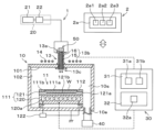
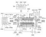
- 1 is a cross-sectional view showing a configuration example of a plasma processing apparatus according to an embodiment
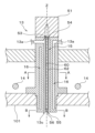
- FIG. 2 is a cross-sectional view showing a configuration example of a light irradiation unit according to an embodiment.
- FIG. 2 is a cross-sectional view showing a configuration example of a light irradiation unit according to an embodiment.
- FIG. 2 is a cross-sectional view showing a configuration example of a light irradiation unit according to an embodiment.
- FIG. 1 shows a schematic diagram of an optical interference system
- 1A and 1B are diagrams illustrating an example of light reflection on the front and back surfaces of a substrate in an optical interference system.
- FIG. 11 is a cross-sectional view showing another configuration example of the plasma processing apparatus in accordance with the embodiment.
- 11 is a cross-sectional view showing an example of a positional relationship of light irradiation units in another configuration example of the plasma processing apparatus in accordance with the embodiment.
- FIG. FIG. 11 is a cross-sectional view showing another configuration example of the plasma processing apparatus in accordance with the embodiment.
- 11 is a cross-sectional view showing an example of a positional relationship of light irradiation units in another configuration example of the plasma processing apparatus in accordance with the embodiment.
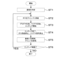
- FIG. 1 is a flowchart showing a configuration example of a plasma etching method according to an embodiment.
- 1 is a sequence chart showing a configuration example of a plasma etching method according to an embodiment.
- a method is known in which a silicon-containing film formed on the surface of a semiconductor wafer (hereinafter referred to as "substrate") is etched using plasma of a processing gas. Also, in the plasma etching process, a method is known in which the substrate is maintained at a low temperature of 0°C or less in order to improve the etching rate of the silicon-containing film.
- various by-products are generated by the reaction between the silicon-containing film and the plasma of the processing gas.
- the volatility of these by-products decreases and they may remain on the substrate. If the by-products remain on the substrate, this may cause etching defects such as deterioration of the etching shape or etch stops due to clogging.
- Patent Document 2 In order to increase the temperature of the substrate, it is possible to temporarily irradiate the substrate with electromagnetic waves during the etching process to heat the substrate, as disclosed in Patent Document 2. However, the method of Patent Document 2 leaves room for improvement in terms of shortening the time it takes to cool the substrate to the process temperature after the entire substrate has been heated.
- the inventors conducted extensive research and discovered that it is possible to sublimate the by-products by maintaining the rest of the substrate at a low temperature and heating only the surface of the substrate. Furthermore, by maintaining the rest of the substrate at a low temperature and heating only the surface of the substrate, the substrate can be cooled immediately after removing the by-products, allowing the next process to be started immediately, which is advantageous from the standpoint of productivity.
- the technology disclosed herein irradiates the substrate with light while maintaining the rest of the substrate at a low temperature, thereby raising the temperature of the substrate's surface and enabling the by-products to be removed efficiently.
- FIG. 1 is a diagram for explaining a configuration example of a plasma processing system.
- the plasma processing system includes a plasma processing device 1 and a control unit 2.
- the plasma processing system is an example of a substrate processing system
- the plasma processing device 1 is an example of a substrate processing device.
- the plasma processing device 1 includes a plasma processing chamber 10, a substrate support unit 11, and a plasma generation unit 12.
- the plasma processing chamber 10 has a plasma processing space.
- the plasma processing chamber 10 also has at least one gas supply port for supplying at least one processing gas to the plasma processing space, and at least one gas exhaust port for exhausting gas from the plasma processing space.
- the gas supply port is connected to a gas supply unit 20 described later, and the gas exhaust port is connected to an exhaust system 40 described later.
- the substrate support unit 11 is disposed in the plasma processing space, and has a substrate support surface for supporting a substrate.
- the plasma generating unit 12 is configured to generate plasma from at least one processing gas supplied into the plasma processing space.
- the plasma formed in the plasma processing space may be inductively coupled plasma (ICP), capacitively coupled plasma (CCP), ECR plasma (Electron-Cyclotron-resonance plasma), helicon wave plasma (HWP), or surface wave plasma (SWP), etc.
- various types of plasma generating units may be used, including AC (Alternating Current) plasma generating units and DC (Direct Current) plasma generating units.
- the AC signal (AC power) used in the AC plasma generating unit has a frequency in the range of 100 kHz to 10 GHz.
- AC signals include RF (Radio Frequency) signals and microwave signals.
- the RF signal has a frequency in the range of 100 kHz to 150 MHz.
- the control unit 2 processes computer-executable instructions that cause the plasma processing apparatus 1 to perform the various steps described in this disclosure.
- the control unit 2 may be configured to control each element of the plasma processing apparatus 1 to perform the various steps described herein. In one embodiment, a part or all of the control unit 2 may be included in the plasma processing apparatus 1.
- the control unit 2 may include a processing unit 2a1, a storage unit 2a2, and a communication interface 2a3.
- the control unit 2 is realized, for example, by a computer 2a.
- the processing unit 2a1 may be configured to perform various control operations by reading a program from the storage unit 2a2 and executing the read program. This program may be stored in the storage unit 2a2 in advance, or may be acquired via a medium when necessary.
- the acquired program is stored in the storage unit 2a2 and is read from the storage unit 2a2 by the processing unit 2a1 and executed.
- the medium may be various storage media readable by the computer 2a, or may be a communication line connected to the communication interface 2a3.
- the processing unit 2a1 may be a CPU (Central Processing Unit).
- the memory unit 2a2 may include a RAM (Random Access Memory), a ROM (Read Only Memory), a HDD (Hard Disk Drive), a SSD (Solid State Drive), or a combination of these.
- the communication interface 2a3 may communicate with the plasma processing device 1 via a communication line such as a LAN (Local Area Network).
- the plasma processing apparatus 1 according to the first embodiment is an inductively coupled plasma processing apparatus.
- the plasma processing apparatus 1 includes a plasma processing chamber 10, a gas supply unit 20, a power source 30, an exhaust system 40, and a light irradiation unit 50.
- the plasma processing chamber 10 includes a dielectric window 101.
- the plasma processing apparatus 1 also includes a substrate support unit 11, a gas introduction unit, and an antenna 14.
- the substrate support unit 11 is disposed within the plasma processing chamber 10.
- the antenna 14 is disposed on or above the plasma processing chamber 10 (i.e., on or above the dielectric window 101).
- the plasma processing chamber 10 has a plasma processing space 10s defined by the dielectric window 101, a sidewall 102 of the plasma processing chamber 10, and the substrate support unit 11.
- the plasma processing chamber 10 is grounded.
- the substrate support 11 includes a main body 111 and a ring assembly 112.
- the main body 111 has a central region 111a for supporting the substrate W and an annular region 111b for supporting the ring assembly 112.
- a wafer is an example of a substrate W.
- the annular region 111b of the main body 111 surrounds the central region 111a of the main body 111 in a plan view.
- the substrate W is disposed on the central region 111a of the main body 111
- the ring assembly 112 is disposed on the annular region 111b of the main body 111 so as to surround the substrate W on the central region 111a of the main body 111. Therefore, the central region 111a is also called a substrate support surface for supporting the substrate W, and the annular region 111b is also called a ring support surface for supporting the ring assembly 112.
- the main body 111 includes a base 120 and an electrostatic chuck 121.
- the base 120 includes a conductive member.
- the conductive member of the base 120 may function as a bias electrode.
- the electrostatic chuck 121 is disposed on the base 120.
- the electrostatic chuck 121 includes a ceramic member 121a and an electrostatic electrode 121b disposed within the ceramic member 121a.
- the ceramic member 121a has a central region 111a. In one embodiment, the ceramic member 121a also has an annular region 111b. Note that other members surrounding the electrostatic chuck 121, such as an annular electrostatic chuck or an annular insulating member, may have the annular region 111b.
- the ring assembly 112 may be disposed on the annular electrostatic chuck or the annular insulating member, or may be disposed on both the electrostatic chuck 121 and the annular insulating member.
- at least one RF/DC electrode coupled to an RF power source 31 and/or a DC power source 32 described later may be disposed in the ceramic member 121a.
- the at least one RF/DC electrode functions as a bias electrode.
- the conductive member of the base 120 and the at least one RF/DC electrode may function as multiple bias electrodes.
- the electrostatic electrode 121b may function as a bias electrode.
- the substrate support 11 includes at least one bias electrode.
- the ring assembly 112 includes one or more annular members.
- the one or more annular members include one or more edge rings and at least one cover ring.
- the edge rings are formed of a conductive or insulating material, and the cover rings are formed of an insulating material.
- the substrate support 11 may also include a temperature adjustment module configured to adjust at least one of the electrostatic chuck 121, the ring assembly 112, and the substrate W to a target temperature.
- the temperature adjustment module may include a heater, a heat transfer medium, a flow passage 120a, or a combination thereof.
- a heat transfer fluid such as brine or a gas flows through the flow passage 120a.
- the flow passage 120a is formed in the base 120, and one or more heaters are disposed in the ceramic member 121a of the electrostatic chuck 121.
- the substrate support 11 may also include a heat transfer gas supply configured to supply a heat transfer gas to a gap between the back surface of the substrate W and the central region 111a.
- a chiller 122 (coolant supply unit) is provided as the heat transfer gas supply unit.
- the coolant supply unit is configured to supply a coolant as a heat transfer medium to the flow path 120a to maintain the substrate at or below the target temperature during plasma generation.
- the target temperature is a temperature that can improve the etching rate of the silicon-containing film in the plasma etching process. As an example, such a temperature is -20°C.
- the chiller 122 is controlled to maintain the coolant supplied to the flow path 120a at or below -20°C.
- the plasma processing apparatus 1 includes at least one heater disposed in the substrate support unit 11 and a heater power supply configured to supply power to the at least one heater.
- the substrate support unit 11 has multiple regions in a plan view, and the at least one heater includes multiple heaters disposed in the multiple regions, respectively.
- the gas introduction section is configured to introduce at least one processing gas from the gas supply section 20 into the plasma processing space 10s.
- the gas introduction section includes a center gas injector (CGI) 13.
- the center gas injector 13 is disposed above the substrate support section 11 and is attached to a central opening formed in the dielectric window 101.
- the center gas injector 13 is formed of a dielectric material such as ceramic or quartz, and has a substantially cylindrical outer shape.
- the center gas injector 13 has at least one gas supply port 13a, at least one gas flow path 13b, and at least one gas inlet port 13c.
- the gas flow path 13b includes a central flow path 15 provided at a position surrounding the housing 52 of the light irradiation unit 50 (described later) in a plan view, and side flow paths 16 provided at a position surrounding the periphery of the central flow path 15 in a plan view.
- the configuration of the gas flow path 13b will be described in detail later.
- the processing gas supplied to the gas supply port 13a passes through the gas flow path 13b and is introduced into the plasma processing space 10s from the gas inlet 13c.
- the processing gas supplied to the central flow path 15 through the gas supply port 13a is sprayed downward from the multiple gas inlets 13c.
- the processing gas supplied to the side flow paths 16 through the gas supply port 13a is sprayed radially from the multiple gas inlets 13c in a direction perpendicular to the Z axis, centered on the Z axis.
- the gas injector may include one or more side gas injectors (SGI) attached to one or more openings formed in the side wall 102.
- SGI side gas injectors
- the gas supply unit 20 may include at least one gas source 21 and at least one flow controller 22.
- the gas supply unit 20 is configured to supply at least one process gas from a corresponding gas source 21 to the gas inlet via a corresponding flow controller 22.
- Each flow controller 22 may include, for example, a mass flow controller or a pressure-controlled flow controller.
- the gas supply unit 20 may include at least one flow modulation device that modulates or pulses the flow rate of the at least one process gas.
- the power supply 30 includes an RF power supply 31 coupled to the plasma processing chamber 10 via at least one impedance matching circuit.
- the RF power supply 31 is configured to supply at least one RF signal (RF power) to at least one bias electrode and the antenna 14. This causes a plasma to be formed from at least one processing gas supplied to the plasma processing space 10s.
- the RF power supply 31 can function as at least a part of the plasma generating unit 12.
- a bias RF signal to at least one bias electrode, a bias potential is generated on the substrate W, and ions in the formed plasma can be attracted to the substrate W.
- the RF power supply 31 includes a first RF generating unit 31a and a second RF generating unit 31b.
- the first RF generating unit 31a is coupled to the antenna 14 via at least one impedance matching circuit and configured to generate a source RF signal (source RF power) for plasma generation.
- the source RF signal has a frequency in the range of 10 MHz to 150 MHz.
- the first RF generating unit 31a may be configured to generate multiple source RF signals having different frequencies. The generated one or more source RF signals are supplied to the antenna 14.
- the second RF generating unit 31b is coupled to at least one bias electrode via at least one impedance matching circuit and configured to generate a bias RF signal (bias RF power).
- the frequency of the bias RF signal may be the same as or different from the frequency of the source RF signal.
- the bias RF signal has a lower frequency than the frequency of the source RF signal.
- the bias RF signal has a frequency in the range of 100 kHz to 60 MHz.
- the second RF generating unit 31b may be configured to generate multiple bias RF signals having different frequencies.
- the generated one or more bias RF signals are supplied to at least one bias electrode.
- at least one of the source RF signal and the bias RF signal may be pulsed.
- the power supply 30 may also include a DC power supply 32 coupled to the plasma processing chamber 10.
- the DC power supply 32 includes a bias DC generator 32a.
- the bias DC generator 32a is connected to at least one bias electrode and configured to generate a bias DC signal. The generated bias DC signal is applied to the at least one bias electrode.
- the bias DC signal may be pulsed.
- a sequence of voltage pulses is applied to at least one bias electrode.
- the voltage pulses may have a rectangular, trapezoidal, triangular, or combination of these pulse waveforms.
- a waveform generator for generating a sequence of voltage pulses from the DC signal is connected between the bias DC generator 32a and at least one bias electrode.
- the bias DC generator 32a and the waveform generator constitute a voltage pulse generator.
- the voltage pulses may have a positive polarity or a negative polarity.
- the sequence of voltage pulses may include one or more positive voltage pulses and one or more negative voltage pulses within one period.
- the bias DC generator 32a may be provided in addition to the RF power source 31 or may be provided instead of the second RF generator 31b.
- the antenna 14 includes one or more coils.
- the antenna 14 may include an outer coil and an inner coil arranged coaxially (so that their central axes Z overlap).
- the RF power supply 31 may be connected to both the outer coil and the inner coil, or to either the outer coil or the inner coil.
- the same RF generating unit may be connected to both the outer coil and the inner coil, or separate RF generating units may be connected separately to the outer coil and the inner coil.
- the exhaust system 40 may be connected to, for example, a gas exhaust port 10e provided at the bottom of the plasma processing chamber 10.
- the exhaust system 40 may include a pressure regulating valve and a vacuum pump. The pressure in the plasma processing space 10s is adjusted by the pressure regulating valve.
- the vacuum pump may include a turbomolecular pump, a dry pump, or a combination thereof.
- the light irradiation unit 50 includes a vertical light source 51 (hereinafter, sometimes referred to as the light source 51) and a housing 52 that transmits light emitted from the light source 51 to the plasma processing chamber 10.
- the housing 52 is provided at a position overlapping the central axis Z of the antenna 14.
- the vertical light source 51 is configured to temporarily and periodically irradiate light to the substrate W on the substrate support 11 in order to heat the substrate W while plasma is being generated in the chamber 10 and while a coolant maintained at -20°C or less is being supplied to the coolant flow path 120a.
- the light from the vertical light source 51 is irradiated vertically.
- the light source 51 emits light having a wavelength of 300 nm to 1100 nm.
- such light source 51 includes a halogen heater lamp.
- the halogen heater lamp can emit light having a wavelength of 300 nm to 1100 nm.
- the thermal energy conversion efficiency is good.
- a thermal energy conversion efficiency of 80 to 90% of the input power can be obtained.
- a tungsten filament is used as a heat source, the temperature can be raised in a short time and the response is high. In addition, heat dissipation loss can be suppressed.
- temperature adjustment by power control is easy, and it is possible to control so as not to heat more than necessary, and energy loss can be suppressed.
- heating is performed only when necessary and turned off when not necessary, it is possible to reduce power consumption.
- halogen lamps have a longer life than general light sources that use filaments, and can emit light stably until the end of their life.
- non-contact heating is performed through a quartz window, there is an advantage that the heated object is not soiled.
- the light source 51 includes a flash lamp.
- the flash lamp may have the configuration described in JP 2020-043180 A. Such a flash lamp is suitable for controlling pulse irradiation, which will be described later.
- the light source 51 includes an LED (Light Emitting Diode). An LED can emit light with high energy efficiency and has a long life.
- the housing 52 has a first window 54 at a first end 53 and a second window 56 at a second end 55.
- the light source 51 and the first end 53 of the central flow passage 15 are connected via the first window 54.
- the plasma processing chamber 10 and the second end 55 of the housing 52 are connected via the second window 56.
- a reflective wall 62 that reflects the light emitted from the light source 51 is formed on the inner wall 60 of the housing 52.
- the reflective wall 62 is formed by evaporating a metal such as aluminum onto the surface of the inner wall 60.
- the first window 54 and the second window 56 are made of a material that transmits the light emitted from the light source 51.
- the first window and the second window may be a light-transmitting material such as quartz (SiO 2 ), sapphire (Al 2 O 3 ), or Y 2 O 3. Quartz, sapphire , Y 2 O 3 , etc. have high light-transmitting properties for light having a wavelength of 300 nm to 1100 nm, and can be used even when the light source 51 emits light having a wavelength of 300 nm to 1100 nm.
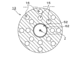
- Figure 4 is a cross-sectional view of the central gas injection section 13 at position A-A in Figure 3, viewed in the direction of the arrow.
- the central axis of the housing 52 is arranged to overlap with the central axis Z of the antenna 14.
- Multiple central flow paths 15 are provided, and are arranged in rotationally symmetric positions so as to surround the housing 52.
- Multiple side flow paths 16 are also provided, and are arranged in rotationally symmetric positions so as to surround the central flow path 15.
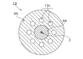
- FIG. 5 is a cross-sectional view of the central gas injection section 13 at position B-B in FIG. 3, viewed in the direction of the arrow.
- a second window 56 is provided at the second end 55.
- a plurality of gas inlets 13c are provided around the second window 56, through which the process gas supplied to the central flow passage 15 passes.
- the plurality of gas inlets 13c are provided at rotationally symmetric positions so as to surround the second window 56.
- the light emitted from the light source 51 passes through the first window 54 and enters the housing 52, travels inside the housing 52 while reflecting off the reflective wall 62, and passes through the second window 56 and is transmitted to the plasma processing chamber 10.
- the light transmitted to the plasma processing chamber 10 is irradiated onto the surface of the substrate W placed on the substrate support 11.
- the second window 56 is shaped as a concave lens. By making the second window 56 shaped as a concave lens, it is possible to refract the light traveling through the central flow path 15 from the direction traveling toward the center of the substrate W to the direction traveling toward the peripheral portion of the substrate W. This allows the second window 56 to diverge radially, and the entire substrate W can be irradiated with light.
- the second window 56 is a hemispherical lens. By making the second window 56 a hemispherical lens, it is possible to refract the light traveling through the central flow path 15 from the direction traveling toward the center of the substrate W to the direction traveling toward the peripheral portion of the substrate W. This allows the second window 56 to diverge radially, and the entire substrate W can be irradiated with light.
- the plasma processing apparatus 1 includes a temperature monitor configured to monitor the temperature of the substrate W on the substrate support 11.
- the temperature monitor includes an optical interference system 100.
- the substrate W is, for example, a wafer made of silicon.
- the electromagnetic wave generated by the light source (monitor light source) is, for example, light (monitor light).
- FIG. 6 is a schematic diagram of an optical interference system 100 according to an exemplary embodiment.
- the optical interference system 100 is applied to a plasma processing apparatus 1.
- At least one window, a first window 82 and a second window 84 in this embodiment, is provided on a sidewall 102 of a chamber 10 of the plasma processing apparatus 1.
- the first window 82 and the second window 84 are provided at opposing positions on the sidewall 102 of the chamber 10. That is, the first window 82 is disposed on the opposite side of the second window 84.
- the optical interference system 100 emits and receives light through the first window 82 and the second window 84 to measure the temperature of the substrate W on the substrate support 11.
- the optical interference system 100 includes a light source 80 as an example of a monitor light source, a focuser 81 as an example of an emission unit, a collimator 85 as an example of a light receiving unit, a spectrometer 86, a memory unit 87, and a control device 88.
- the light source 80 is either a low-coherence light source or a tunable light source configured to emit light that can transmit through the substrate W on the substrate support 11.
- a low-coherence light source is a light source that generates light with a coherence length of the order of microns or less.
- a low-coherence light source is a light source with a coherence length of several tens of ⁇ m.
- a low-coherence light source is an SLD (super luminescent diode).
- a tunable light source is a light source that can freely change the wavelength of the light it generates.
- the focuser 81 is provided outside the chamber 10 and configured to emit light (monitor light) generated by the light source 80 toward the substrate W on the substrate support 11.
- the focuser 81 is connected to the light source 80 via an optical fiber or the like.
- the light generated by the light source 80 propagates to the focuser 81 via the optical fiber.
- the focuser 81 emits light toward the substrate W on the substrate support 11 through a first window 82 (see the dashed dotted line in the figure).
- the focuser 81 is positioned so that light reflected from the front and back surfaces of the substrate W on the substrate support 11 enters the second window 84.
- the focuser 81 may be a collimator.
- the collimator 85 is provided outside the chamber 10 and configured to receive reflected light from the substrate W.
- the collimator 85 is disposed on the opposite side of the focuser 81 across the substrate W.
- the collimator 85 receives the reflected light from the substrate W on the substrate support 11 through the second window 84.
- the collimator 85 is connected to the spectroscope 86 through an optical fiber or the like.
- the collimator 85 receives the reflected light and propagates the light to the spectroscope 86 through an optical fiber or the like.
- the collimator 85 may be a focuser.
- FIG. 7 is a diagram showing an example of reflection on the front surface Wa and rear surface Wb of the substrate W. As shown in FIG. 7, the light incident on the substrate W is reflected by the front surface Wa of the substrate W and also by the rear surface Wb of the substrate W. The reflected light becomes interference light including the reflected light from each of the two parallel reflecting surfaces.
- the spectrometer 86 is configured to detect the spectrum of the reflected light received by the collimator 85.
- the spectrometer 86 has, for example, a spectroscopic mechanism and a detection unit.
- the spectroscopic mechanism disperses light at a predetermined dispersion angle for each wavelength.
- An example of the spectroscopic mechanism is a diffraction grating.
- the detection unit detects the light dispersed by the spectroscopic mechanism.
- An example of the detection unit is a CCD (Charge Coupled Device). The number of elements in the CCD is the sampling number.
- the detection unit detects the intensity of the reflected light for each wavelength as a spectrum.
- the spectrum may be a reflectance curve that indicates the relationship between wavelength and reflectance. Once the reflectance curve is detected, the temperature of the substrate W is calculated from the correlation.
- the memory unit 87 is configured to store in advance the relationship between the reflectance curve and temperature.
- the relationship between the reflectance curve and temperature is reference data and is obtained in advance.
- the memory unit 87 may store the relationship between the reflectance curve and temperature for each material.
- the control device 88 is connected to the spectrometer 86 and the memory unit 87.
- the control device 88 is configured to calculate the temperature of the substrate W based on the reflectance curve detected by the spectrometer 86 and the relationship stored in the memory unit 87.
- the control device 88 may be a computer equipped with a processor, a memory unit, an input device, a display device, etc. In one embodiment, the control device 88 is included in the control unit 2.
- the temperature monitor (optical interference system 100) therefore includes a monitor light source (light source 80), an emission section (focuser 81) and a light receiving section (collimator 85).
- the monitor light source (light source 80) is configured to emit electromagnetic waves that can pass through the substrate W on the substrate support section 11.
- the emission section (focuser 81) is configured to emit the electromagnetic waves generated by the monitor light source (light source 80) obliquely to the substrate W on the substrate support section 11.
- the light receiving section (collimator 85) is disposed on the opposite side of the emission section (focuser 81) and is configured to receive reflected waves reflected from the front and back surfaces of the substrate W on the substrate support section 11.
- the control section 2 is then configured to determine the temperature of the substrate W on the substrate support section 11 based on the reflected waves that are incident on the light receiving section (collimator 85).
- the optical interference system 100 may use either a spectroscopic method or a wavelength scanning method.
- the spectroscopic method uses a broadband light source such as an SLD or an ASE (Amplified Spontaneous Emission), disperses the light using a grating or the like, and acquires the spectrum using a CCD (Charge Coupled Device) array or the like.
- the wavelength scanning method uses a narrowband light source that can control the wavelength of the output light to scan the wavelength of the output light, and receives the light using a photodiode or the like.
- the optical interference system 100 may have a mechanism for adjusting the optical axis.
- the focuser 81 may be supported by a first adjustment mechanism 81a.
- the first adjustment mechanism 81a is a mechanism that can adjust the emission direction of the focuser 81.
- the first adjustment mechanism 81a is a three-axis stage that is movable in the X-axis, Y-axis, and Z-axis.
- the collimator 85 may be supported by a second adjustment mechanism 81b.
- the second adjustment mechanism 81b may have the same configuration as the first adjustment mechanism 81a.
- control unit 2 is configured to control the coolant supply unit, the heater power supply, and/or the at least one light source 51 to adjust the first temperature of the coolant, the power supplied to at least one heater, and/or the intensity of light irradiated to the substrate W on the substrate support unit 11 based on the output of the temperature monitor.
- control unit 2 is configured to control the heater power supplies to adjust the power supplied to each of the heaters to correct non-uniformity in temperature of the substrate W on the substrate support unit 11 caused by the irradiation of light based on the output of the temperature monitor.
- the other embodiments described below may also include a temperature monitor having a similar configuration.
- the light irradiation unit 50 is provided above the substrate W and facing the substrate W, thereby shortening the average distance between the second window 56 in the light irradiation unit 50 and the substrate W. This allows the light emitted from the light source 51 to be efficiently irradiated onto the substrate W. Furthermore, since the light irradiation unit 50 is positioned so as to overlap with the central axis Z of the antenna, the distance between the second window 56 in the light irradiation unit 50 and the center or periphery of the substrate W becomes uniform. This makes it possible to irradiate the substrate W with light evenly.
- an RF signal is supplied to the antenna 14, which induces an electromagnetic field, thereby generating plasma.
- placing a component other than the antenna 14 above the plasma processing chamber 10 in which the antenna 14 is located may hinder the induction of the electromagnetic field, and may be a factor in preventing the generation or maintenance of plasma.
- the inventors conducted extensive research and discovered that the problem can be solved by configuring the light irradiation unit 50 as described above.
- the housing 52 of the light irradiation unit 50 is arranged so as to overlap the central axis Z of the antenna 14, so that the effect of providing the light irradiation unit 50 on the electromagnetic field can be reduced.
- the light irradiated onto the surface of the substrate W is absorbed by the material that constitutes the substrate W, and the temperature of the region containing the material rises.
- light absorption refers to a state in which the amplitude of the molecular vibration of the material is promoted and the material retains high thermal energy when the frequency of the irradiated light matches the inherent frequency that depends on the bonding strength between the atoms of the material (e.g., silicon), resulting in a state in which the material retains high thermal energy. This state can be called a state in which light is absorbed and heated.
- silicon when the film to be etched is a silicon-containing film, silicon has a band gap energy of about 1.1 eV, and absorbs near-infrared light and visible light with wavelengths shorter than 1100 nm well, but hardly absorbs infrared light with wavelengths longer than 1100 nm. For this reason, when the light source 51 emits light with a wavelength of 300 nm to 1100 nm, silicon-containing films such as Si and SiN, which have high absorbance for the light, absorb the light, and the temperature of the region containing the material on the substrate W rises. Tungsten also absorbs light from 300 nm to 1100 nm, causing the temperature of the tungsten-containing areas of the substrate W to rise.
- the heat is conducted to the by-products generated by the plasma etching and attached to the substrate, causing the by-products to sublimate.
- the increase in temperature of the substrate W promotes the etching reaction.
- the film to be etched is a silicon-containing film such as a Si film, a SiO2 film, or a SiN film
- CO ammonium fluorosilicate
- SiF4 , SiH4 , NH3 , or SiH4 may be generated as by-products.
- a low temperature e.g., -20°C
- SiH4 and AFS may adhere to the surface of the substrate W as by-products.
- the temperature at which the by-products can be sublimated is, for example, 100°C or higher.
- the sublimated by-products that have become gaseous are, for example, exhausted outside the plasma processing chamber 10 by the exhaust system 40.
- FIG. 8 is a cross-sectional view showing an example of the configuration of the plasma processing apparatus 200.
- Figure 9 is an explanatory diagram showing an example of the positional relationship of the light irradiation units when the plasma processing apparatus 200 is viewed from above.
- the plasma processing apparatus 200 according to the second embodiment is an inductively coupled plasma processing apparatus, and has the same configuration as the plasma processing apparatus 1 according to the first embodiment except for the configuration of the first to third light irradiation units 201a to 201c, and exerts the same actions and effects.
- the first light irradiation unit 201a, the second light irradiation unit 201b, and the third light irradiation unit 201c each include a first oblique light source 202a, a second oblique light source 202b, and a third oblique light source 202c (hereinafter, these may be collectively referred to as oblique light source 202).
- the plasma processing apparatus 200 includes at least one light source.
- the at least one light source includes a vertical light source 51 and a plurality of oblique light sources 202a, 202b, and 202c.
- the plurality of oblique light sources 202a, 202b, and 202c are arranged in the circumferential direction along the side wall 102 of the plasma processing chamber 10. In one embodiment, the plurality of oblique light sources 202a, 202b, and 202c are arranged at equal intervals in the circumferential direction.
- the oblique light sources 202a, 202b, and 202c are configured to temporarily and periodically irradiate the substrate W on the substrate support 11 with light to heat the substrate W while plasma is generated in the chamber 10 and while a coolant maintained at ⁇ 20° C. or less is supplied to the coolant passage 1110a.
- the light from the oblique light sources 202a, 202b, and 202c is irradiated in an oblique direction.
- the first light irradiation unit 201a includes a first light source 202a and a first housing 203a that transmits the light emitted from the first light source 202a to the plasma processing chamber 10.
- the second light irradiation unit 201b includes a second light source 202b and a second housing 203b
- the third light irradiation unit 201c includes a third light source 202c and a third housing 203c.
- the first housing 203a has a first end connected to the first light source 202a and a second end connected to a window 210a provided in the side wall 102 of the plasma processing chamber 10.
- a first reflecting wall 204a that reflects the light emitted from the first light source 202a is formed on the inner wall of the first housing 203a.
- the first reflecting wall 204a is formed by evaporating a metal such as aluminum onto the surface of the inner wall. The same is true for the second housing 203b and the third housing 203c.
- the multiple oblique light sources 202a, 202b, and 202c may be arranged at rotationally symmetric positions in a plan view of the plasma processing chamber 10.
- the light irradiation unit 201 having the above configuration, light emitted from the oblique light source 202 enters the housing 203, travels inside the housing 203 while reflecting off the reflecting wall 208, and is transmitted through the window 210 to the plasma processing chamber 10. The light transmitted to the plasma processing chamber 10 is irradiated onto the surface of the substrate W placed on the substrate support 11.
- the oblique light source 202 may be a halogen heater lamp, a flash lamp, or an LED as described in the first embodiment.
- the plasma processing apparatus 300 according to the third embodiment is a capacitively coupled plasma processing apparatus.
- Fig. 10 is a cross-sectional view showing an example of the configuration of the plasma processing apparatus 300.
- Fig. 11 is an explanatory diagram showing an example of the positional relationship of the light irradiation unit 350 when the plasma processing apparatus 300 is viewed from above.
- the capacitively coupled plasma processing apparatus 300 includes a plasma processing chamber 310, a gas supply unit 320, a power source 330, an exhaust system 340, and a plurality of light irradiation units 350a-350c (hereinafter sometimes referred to as light irradiation unit 350).
- the plasma processing apparatus 300 also includes a substrate support unit 311 and a gas introduction unit.
- the gas introduction unit is configured to introduce at least one processing gas into the plasma processing chamber 310.
- the gas introduction unit includes a shower head 313.
- the substrate support unit 311 is disposed in the plasma processing chamber 310.
- the shower head 313 is disposed above the substrate support unit 311. In one embodiment, the shower head 313 constitutes at least a part of the ceiling of the plasma processing chamber 310.
- the plasma processing chamber 310 has a plasma processing space 310s defined by the shower head 313, the sidewall 312 of the plasma processing chamber 310, and the substrate support unit 311.
- the plasma processing chamber 310 is grounded.
- the showerhead 313 and the substrate support 311 are electrically insulated from the housing of the plasma processing chamber 310.
- the substrate support portion 311 includes a main body portion 321 and a ring assembly 322.
- the main body portion 321 has a central region 321a for supporting the substrate W and an annular region 321b for supporting the ring assembly 322.
- the annular region 321b of the main body portion 321 surrounds the central region 321a of the main body portion 321 in a plan view.
- the substrate W is disposed on the central region 321a of the main body portion 321, and the ring assembly 322 is disposed on the annular region 321b of the main body portion 321 so as to surround the substrate W on the central region 321a of the main body portion 321. Therefore, the central region 321a is also called a substrate support surface for supporting the substrate W, and the annular region 321b is also called a ring support surface for supporting the ring assembly 322.
- the main body 321 includes a base 324 and an electrostatic chuck 325.
- the base 324 includes a conductive member.
- the conductive member of the base 324 may function as a lower electrode.
- the electrostatic chuck 325 is disposed on the base 324.
- the electrostatic chuck 325 includes a ceramic member 325a and an electrostatic electrode 325b disposed within the ceramic member 325a.
- the ceramic member 325a has a central region 321a. In one embodiment, the ceramic member 325a also has an annular region 321b. Note that other members surrounding the electrostatic chuck 325, such as an annular electrostatic chuck or an annular insulating member, may have the annular region 321b.
- the ring assembly 322 may be disposed on the annular electrostatic chuck or the annular insulating member, or may be disposed on both the electrostatic chuck 325 and the annular insulating member.
- At least one RF/DC electrode coupled to an RF power source 341 and/or a DC power source 342, which will be described later, may be disposed within the ceramic member 325a.
- the at least one RF/DC electrode functions as a lower electrode.
- the RF/DC electrode is also called a bias electrode.
- the conductive member of the base 324 and the at least one RF/DC electrode may function as multiple lower electrodes.
- the electrostatic electrode 325b may function as the lower electrode.
- the substrate support 311 includes at least one lower electrode.
- the ring assembly 322 includes one or more annular members.
- the one or more annular members include one or more edge rings and at least one cover ring.
- the edge rings are formed of a conductive or insulating material, and the cover rings are formed of an insulating material.
- the substrate support 311 may also include a temperature adjustment module configured to adjust at least one of the electrostatic chuck 325, the ring assembly 322, and the substrate W to a target temperature.
- the temperature adjustment module may include a heater, a heat transfer medium, a flow passage 324a, or a combination thereof.
- a heat transfer fluid such as brine or a gas flows through the flow passage 324a.
- the flow passage 324a is formed in the base 324, and one or more heaters are disposed in the ceramic member 325a of the electrostatic chuck 325.
- the substrate support 311 may also include a heat transfer gas supply configured to supply a heat transfer gas to a gap between the back surface of the substrate W and the central region 321a.
- a chiller 326 (coolant supply unit) is provided as the heat transfer gas supply unit.
- the coolant supply unit is configured to supply a coolant as a heat transfer medium to the flow path 324a, thereby maintaining the substrate at or below the target temperature during plasma generation.
- the target temperature is a temperature that can improve the etching rate of the silicon-containing film in the plasma etching process. As an example, such a temperature is -20°C.
- the chiller 326 is controlled to maintain the coolant supplied to the flow path 120a at or below -20°C.
- the shower head 313 is configured to introduce at least one processing gas from the gas supply unit 320 into the plasma processing space 310s.
- the shower head 313 has at least one gas supply port 313a, at least one gas diffusion chamber 313b, and multiple gas inlets 313c.
- the processing gas supplied to the gas supply port 313a passes through the gas diffusion chamber 313b and is introduced into the plasma processing space 310s from the multiple gas inlets 313c.
- the shower head 313 also includes at least one upper electrode.
- the gas introduction unit may include, in addition to the shower head 313, one or more side gas injectors (SGIs) attached to one or more openings formed in the sidewall 312.
- SGIs side gas injectors
- the gas supply 320 may include at least one gas source 331 and at least one flow controller 332.
- the gas supply 320 is configured to supply at least one process gas from a respective gas source 331 through a respective flow controller 332 to the showerhead 313.
- Each flow controller 332 may include, for example, a mass flow controller or a pressure-controlled flow controller.
- the gas supply 320 may include at least one flow modulation device to modulate or pulse the flow rate of the at least one process gas.
- the power supply 330 includes an RF power supply 341 coupled to the plasma processing chamber 310 via at least one impedance matching circuit.
- the RF power supply 341 is configured to supply at least one RF signal (RF power) to at least one lower electrode and/or at least one upper electrode. This causes a plasma to be formed from at least one processing gas supplied to the plasma processing space 310s.
- the RF power supply 341 can function as at least a part of the plasma generating unit 12.
- a bias RF signal to at least one lower electrode, a bias potential is generated on the substrate W, and ion components in the formed plasma can be attracted to the substrate W.
- the RF power supply 341 includes a first RF generating unit 341a and a second RF generating unit 341b.
- the first RF generating unit 341a is coupled to at least one lower electrode and/or at least one upper electrode via at least one impedance matching circuit and configured to generate a source RF signal (source RF power) for plasma generation.
- the source RF signal has a frequency in the range of 10 MHz to 150 MHz.
- the first RF generating unit 341a may be configured to generate multiple source RF signals having different frequencies. The generated one or more source RF signals are supplied to at least one lower electrode and/or at least one upper electrode.
- the second RF generator 341b is coupled to at least one lower electrode via at least one impedance matching circuit and configured to generate a bias RF signal (bias RF power).
- the frequency of the bias RF signal may be the same as or different from the frequency of the source RF signal.
- the bias RF signal has a lower frequency than the frequency of the source RF signal.
- the bias RF signal has a frequency in the range of 100 kHz to 60 MHz.
- the second RF generator 341b may be configured to generate multiple bias RF signals having different frequencies.
- the generated one or more bias RF signals are provided to at least one lower electrode. Also, in various embodiments, at least one of the source RF signal and the bias RF signal may be pulsed.
- the power supply 330 may also include a DC power supply 342 coupled to the plasma processing chamber 310.
- the DC power supply 342 includes a first DC generator 342a and a second DC generator 342b.
- the first DC generator 342a is connected to at least one lower electrode and configured to generate a first DC signal.
- the generated first DC signal is applied to the at least one lower electrode.
- the second DC generator 342b is connected to at least one upper electrode and configured to generate a second DC signal.
- the generated second DC signal is applied to the at least one upper electrode.
- the first and second DC signals may be pulsed.
- a sequence of voltage pulses is applied to at least one lower electrode and/or at least one upper electrode.
- the voltage pulses may have a rectangular, trapezoidal, triangular or combination thereof pulse waveform.
- a waveform generator for generating a sequence of voltage pulses from the DC signal is connected between the first DC generator 342a and at least one lower electrode.
- the first DC generator 342a and the waveform generator constitute a voltage pulse generator.
- the second DC generator 342b and the waveform generator constitute a voltage pulse generator
- the voltage pulse generator is connected to at least one upper electrode.
- the voltage pulses may have a positive polarity or a negative polarity.
- the sequence of voltage pulses may also include one or more positive polarity voltage pulses and one or more negative polarity voltage pulses within one period.
- the first and second DC generating units 342a and 342b may be provided in addition to the RF power supply 341, or the first DC generating unit 342a may be provided in place of the second RF generating unit 341b.
- the exhaust system 340 may be connected to, for example, a gas exhaust port 310e provided at the bottom of the plasma processing chamber 310.
- the exhaust system 340 may include a pressure regulating valve and a vacuum pump. The pressure in the plasma processing space 310s is adjusted by the pressure regulating valve.
- the vacuum pump may include a turbomolecular pump, a dry pump, or a combination thereof.
- the first light irradiation unit 350a, the second light irradiation unit 350b, and the third light irradiation unit 350c each include a first oblique light source 351a, a second oblique light source 351b, and a third oblique light source 351c (hereinafter, these may be collectively referred to as oblique light source 351).
- the plasma processing apparatus 300 includes a plurality of oblique light sources 351a, 351b, and 351c.
- the plurality of oblique light sources 351a, 351b, and 351c are arranged in the circumferential direction along the side wall 312 of the plasma processing chamber 310.
- the plurality of oblique light sources 351a, 351b, and 351c are arranged at equal intervals in the circumferential direction.
- the oblique light sources 351a, 351b, and 351c are configured to temporarily and periodically irradiate the substrate W on the substrate support 311 with light while plasma is generated in the chamber 310 and while a coolant maintained at ⁇ 20° C. or lower is supplied to the coolant passage 324a to heat the substrate W.
- the light from the oblique light sources 351a, 351b, and 351c is irradiated in an oblique direction.
- the first light irradiating unit 350a includes a first light source 351a and a first housing 353a that transmits the light emitted from the first light source 351a to the plasma processing chamber 310.
- the second light irradiating unit 350b includes a second light source 351b and a second housing 353b
- the third light irradiating unit 350c includes a third light source 351c and a third housing 353c.
- the first housing 353a has a first end connected to the first light source 351a and a second end connected to a window 360a provided in the side wall 312 of the plasma processing chamber 310.
- a first reflecting wall 354a that reflects the light emitted from the first light source 351a is formed on the inner wall of the first housing 353a.
- the first reflecting wall 354a is formed by evaporating a metal such as aluminum onto the surface of the inner wall. The same is true for the second housing 353b and the third housing 353c.
- the multiple oblique light sources 351a, 351b, and 351c may be arranged at rotationally symmetric positions in a plan view of the plasma processing chamber 310.
- the oblique light source 351 may be a halogen heater lamp, a flash lamp, or an LED as described in the first embodiment.
- light emitted from the oblique light source 351 enters the housing 353, travels inside the housing 353 while reflecting off the reflecting wall 363, and is transmitted through the window 360 to the plasma processing chamber 310.
- the light transmitted to the plasma processing chamber 310 is irradiated onto the surface of the substrate W placed on the substrate support part 311.
- Fig. 12 is a flow chart showing a configuration example of the plasma etching method.
- Fig. 13 is a sequence chart showing a configuration example of the plasma etching method.
- the plasma etching method can be performed using a plasma processing system including any one selected from the plasma processing apparatuses according to the first to third embodiments. Note that the following arbitrary operations, measurements, commands, and other controls can be performed using the control unit 2.
- the coolant supply unit is controlled to supply a coolant to the flow path 120a to maintain the bases 120, 324, the electrostatic chucks 121, 325, and the substrate W at ⁇ 20° C. or lower.
- the film to be etched is a silicon-containing film such as a Si film, a SiO 2 film, or a SiN film
- the substrate W can be etched at a high etching rate by cooling the temperature of the substrate W to ⁇ 20° C. or lower and etching the substrate W.
- the etching process gas is started to be supplied from the gas inlet into the plasma processing chamber 10, 310 at the desired pressure and flow rate.
- a plasma is generated in the plasma processing chamber 10, 310 by supplying an RF signal from the RF power supply 31, 341 to the antenna 14 (first or second embodiment) or to the upper and lower electrodes (third embodiment).
- a bias RF signal is supplied from the RF power supply 31, 341 to the substrate support 11, 311, and etching is initiated by attracting ions to the substrate W.
- step ST4 once the desired etching process of the substrate W is completed in step ST3, the supply of the process gas is stopped and the supply of the bias RF signal is stopped.
- the substrate W is irradiated with light from the light irradiation units 50, 201, and 350.
- the light irradiation may be performed by either steady irradiation or pulse irradiation, or a combination of these.
- the light irradiation units 50, 201, 350 are controlled to emit light at all times while the process ST5 is continuing.
- the light irradiation units 50, 201, 350 may be controlled to emit light until the temperature of the surface layer of the substrate W reaches 100°C or higher.
- the time required for all by-products to be sublimated and removed may be empirically measured, and the light irradiation units 50, 201, 350 may be controlled to emit light for that time.
- the steady-state irradiation when a halogen heater lamp is used as the light source, the time is, for example, 10 seconds. In this case, the intensity of the light emitted from the light source is adjusted so that the temperature of the surface layer of the substrate W reaches the temperature at which the by-products sublimate within 10 seconds.
- the plasma processing chamber 10, 310 is evacuated. This allows the sublimated by-products to be discharged outside the plasma processing chamber 10, 310.
- step ST6 a decision is made as to whether or not to continue plasma etching based on the desired recipe. If plasma etching is to be continued, the process returns to step ST2 and steps ST2 to ST6 are executed again. If plasma etching is not to be continued, the process ends.
- the output of a temperature monitor related to the temperature of the substrate is acquired. Also, based on the output of the temperature monitor, at least one of the first temperature of the coolant, the power supplied to at least one heater, or the intensity of the light irradiated to the substrate on the substrate support is adjusted.
- the output of a temperature monitor related to the temperature of the substrate is acquired during the execution of the fifth step ST5. Based on the output of the temperature monitor, the power supplied to each of the plurality of heaters is adjusted to correct the unevenness in the temperature of the substrate on the substrate support portion caused by the irradiation of light. That is, when it is detected that the temperatures of the substrate areas corresponding to the plurality of regions of the substrate support portion are different from one another, the temperature of each of the plurality of heaters corresponding to each of the substrate areas is adjusted so as to correct the unevenness in the temperature of each of the substrate areas.
- the unevenness in the temperature of each of the substrate areas can be corrected, for example, by lowering the temperature of the corresponding heater when one region is hotter than the desired temperature, and by raising the temperature of the other corresponding heater when another region is colder than the desired temperature.
- a chamber a substrate support disposed within the chamber and having a coolant flow path; a dielectric window disposed above the substrate support; an antenna disposed above the dielectric window; an RF power source configured to provide an RF signal to the antenna to generate a plasma in the chamber; a coolant supply configured to supply a coolant maintained at a first temperature to the coolant flow path; at least one heater disposed within the substrate support; a heater power supply configured to supply power to the at least one heater; at least one light source configured to temporarily and periodically irradiate the substrate on the substrate support with light while the plasma is generated in the chamber and while the coolant maintained at the first temperature is supplied to the coolant passage; and a temperature monitor configured to monitor a temperature of the substrate on the substrate support; a controller configured to control the coolant supply, the heater power supply, and/or the at least one light source to adjust the first temperature of the coolant, the power supplied to the at least one heater, and/or the
- a substrate on the substrate support is etched by the plasma, thereby forming by-products on the substrate;
- the plasma processing apparatus according to claim 1 or 2 wherein the by-products on the substrate are sublimated by the light.
- the plasma processing apparatus according to (3) above wherein the substrate on the substrate support is heated to 100° C. or higher by the light.
- a substrate on the substrate support is etched by the plasma; The plasma processing apparatus according to the above (1) or (2), wherein the light promotes an etching reaction.
- the plasma processing apparatus according to any one of (1) to (6) above, wherein the light has a wavelength in the range of 300 nm to 1100 nm.
- the at least one light source includes a first light source arranged to overlap a central axis of the antenna.
- the at least one light source includes a plurality of light sources arranged circumferentially along a sidewall of the chamber.
- the first light source includes a hemispherical lens.
- each of the plurality of light sources includes a hemispherical lens.
- the at least one light source includes a halogen heater lamp.
- the at least one light source includes a flash lamp.
- the at least one light source includes an LED.
- the substrate support portion has a plurality of regions in a plan view, the at least one heater includes a plurality of heaters disposed in the plurality of regions,
- the temperature monitor a monitor light source configured to emit electromagnetic waves capable of penetrating the substrate on the substrate support; an emission unit configured to emit the electromagnetic wave generated by the monitor light source obliquely toward the substrate on the substrate support unit; a light receiving unit disposed on the opposite side of the light emitting unit across the substrate and configured to receive reflected waves reflected by the front and back surfaces of the substrate on the substrate support unit;
- the plasma processing apparatus according to any one of (1) to (15) above, wherein the control unit is configured to determine a temperature of the substrate on the substrate support unit based on the reflected wave incident on the light receiving unit.
- a chamber a substrate support disposed within the chamber and having a coolant flow path; a plasma generating unit having an RF power source for generating plasma in the chamber; a coolant supply configured to supply a coolant maintained at a first temperature to the coolant flow path to cool the substrate on the substrate support; at least one light source configured to temporarily and periodically irradiate the substrate on the substrate support with light while the plasma is generated in the chamber and while the coolant maintained at the first temperature is supplied to the coolant passage; and
- a plasma processing apparatus comprising: (18) The plasma processing apparatus according to (17) above, wherein the first temperature is ⁇ 20° C. or lower.
- a substrate on the substrate support is etched by the plasma, thereby forming by-products on the substrate; and The plasma processing apparatus according to claim 18, wherein the by-products on the substrate are sublimated by the light.
- the plasma processing apparatus according to any one of (17) to (20) above, wherein the light has a wavelength in the range of 300 nm to 1100 nm.
- the at least one light source includes a plurality of light sources arranged circumferentially along a sidewall of the chamber.
- a coolant supply unit that supplies a coolant to a coolant flow path in the substrate support unit is controlled to maintain the substrate at ⁇ 20° C. or lower;
- the method includes a step of controlling a light irradiation unit to irradiate the substrate with light and temporarily and periodically heat the substrate. Plasma etching method.
- REFERENCE SIGNS LIST 1 200, 300 Plasma processing apparatus 2 Control unit 10, 310 Plasma processing chamber 11, 311 Substrate support unit 14 Antenna 31, 341 RF power supply 50, 201, 350 Light irradiation unit 51, 202, 351 Light source 100 Optical interference system 101 Dielectric window W Substrate
Landscapes
- Physics & Mathematics (AREA)
- Engineering & Computer Science (AREA)
- Plasma & Fusion (AREA)
- Chemical & Material Sciences (AREA)
- Analytical Chemistry (AREA)
- Health & Medical Sciences (AREA)
- Epidemiology (AREA)
- Public Health (AREA)
- Drying Of Semiconductors (AREA)
Priority Applications (3)
| Application Number | Priority Date | Filing Date | Title |
|---|---|---|---|
| JP2024574836A JPWO2024162171A1 (https=) | 2023-02-03 | 2024-01-25 | |
| TW113103674A TW202503828A (zh) | 2023-02-03 | 2024-01-31 | 電漿處理裝置及電漿蝕刻方法 |
| US19/278,865 US20250349524A1 (en) | 2023-02-03 | 2025-07-24 | Plasma processing apparatus and plasma etching method |
Applications Claiming Priority (2)
| Application Number | Priority Date | Filing Date | Title |
|---|---|---|---|
| JP2023015672 | 2023-02-03 | ||
| JP2023-015672 | 2023-02-03 |
Related Child Applications (1)
| Application Number | Title | Priority Date | Filing Date |
|---|---|---|---|
| US19/278,865 Continuation US20250349524A1 (en) | 2023-02-03 | 2025-07-24 | Plasma processing apparatus and plasma etching method |
Publications (1)
| Publication Number | Publication Date |
|---|---|
| WO2024162171A1 true WO2024162171A1 (ja) | 2024-08-08 |
Family
ID=92146646
Family Applications (1)
| Application Number | Title | Priority Date | Filing Date |
|---|---|---|---|
| PCT/JP2024/002218 Ceased WO2024162171A1 (ja) | 2023-02-03 | 2024-01-25 | プラズマ処理装置及びプラズマエッチング方法 |
Country Status (4)
| Country | Link |
|---|---|
| US (1) | US20250349524A1 (https=) |
| JP (1) | JPWO2024162171A1 (https=) |
| TW (1) | TW202503828A (https=) |
| WO (1) | WO2024162171A1 (https=) |
Cited By (1)
| Publication number | Priority date | Publication date | Assignee | Title |
|---|---|---|---|---|
| US20240062991A1 (en) * | 2021-04-23 | 2024-02-22 | Tokyo Electron Limited | Plasma processing apparatus and substrate processing method |
Citations (4)
| Publication number | Priority date | Publication date | Assignee | Title |
|---|---|---|---|---|
| JPH05251397A (ja) * | 1992-03-05 | 1993-09-28 | Fujitsu Ltd | 基板温度の測定方法 |
| JPH08222549A (ja) * | 1995-02-16 | 1996-08-30 | Sony Corp | プラズマ処理装置およびプラズマ処理方法 |
| JP2020043180A (ja) * | 2018-09-07 | 2020-03-19 | 東京エレクトロン株式会社 | 基板処理装置及び基板処理方法 |
| WO2020110192A1 (ja) * | 2018-11-27 | 2020-06-04 | 株式会社日立ハイテクノロジーズ | プラズマ処理装置及びそれを用いた試料の処理方法 |
-
2024
- 2024-01-25 WO PCT/JP2024/002218 patent/WO2024162171A1/ja not_active Ceased
- 2024-01-25 JP JP2024574836A patent/JPWO2024162171A1/ja active Pending
- 2024-01-31 TW TW113103674A patent/TW202503828A/zh unknown
-
2025
- 2025-07-24 US US19/278,865 patent/US20250349524A1/en active Pending
Patent Citations (4)
| Publication number | Priority date | Publication date | Assignee | Title |
|---|---|---|---|---|
| JPH05251397A (ja) * | 1992-03-05 | 1993-09-28 | Fujitsu Ltd | 基板温度の測定方法 |
| JPH08222549A (ja) * | 1995-02-16 | 1996-08-30 | Sony Corp | プラズマ処理装置およびプラズマ処理方法 |
| JP2020043180A (ja) * | 2018-09-07 | 2020-03-19 | 東京エレクトロン株式会社 | 基板処理装置及び基板処理方法 |
| WO2020110192A1 (ja) * | 2018-11-27 | 2020-06-04 | 株式会社日立ハイテクノロジーズ | プラズマ処理装置及びそれを用いた試料の処理方法 |
Cited By (2)
| Publication number | Priority date | Publication date | Assignee | Title |
|---|---|---|---|---|
| US20240062991A1 (en) * | 2021-04-23 | 2024-02-22 | Tokyo Electron Limited | Plasma processing apparatus and substrate processing method |
| US12387907B2 (en) * | 2021-04-23 | 2025-08-12 | Tokyo Electron Limited | Plasma processing apparatus and substrate processing method |
Also Published As
| Publication number | Publication date |
|---|---|
| TW202503828A (zh) | 2025-01-16 |
| US20250349524A1 (en) | 2025-11-13 |
| JPWO2024162171A1 (https=) | 2024-08-08 |
Similar Documents
| Publication | Publication Date | Title |
|---|---|---|
| US12315704B2 (en) | Plasma processing apparatus, and method and program for controlling elevation of focus ring | |
| US10998244B2 (en) | System and method for temperature control in plasma processing system | |
| US8486221B2 (en) | Focus ring heating method, plasma etching apparatus, and plasma etching method | |
| JP2019186400A (ja) | プラズマ処理装置、プラズマ制御方法、及びプラズマ制御プログラム | |
| US20160225645A1 (en) | Temperature control mechanism, temperature control method and substrate processing apparatus | |
| US20170316963A1 (en) | Direct optical heating of substrates | |
| US20220005678A1 (en) | Substrate processing apparatus, reflector and method of manufacturing semiconductor device | |
| US20250349524A1 (en) | Plasma processing apparatus and plasma etching method | |
| US11217430B2 (en) | Plasma processing apparatus and plasma processing method | |
| JP2008182102A (ja) | 天板部材及びこれを用いたプラズマ処理装置 | |
| US12523546B2 (en) | Measurement apparatus, measurement system, substrate processing apparatus, and measurement method | |
| KR102818934B1 (ko) | 기판 처리 장치 및 조사 위치 조정 방법 | |
| KR102508230B1 (ko) | 플라스마 처리 장치 및 플라스마 처리 방법 | |
| US20250210316A1 (en) | Substrate processing apparatus using microwaves | |
| TWI894663B (zh) | 基座組件及電漿處理裝置 | |
| TWI899429B (zh) | 基板支持器、電漿處理系統及電漿蝕刻方法 | |
| KR20220058782A (ko) | 마이크로웨이브 유닛 및 그를 포함하는 기판 처리 장치 | |
| US12518953B2 (en) | Plasma processing apparatus and method of manufacture | |
| TWI917607B (zh) | 電漿處理裝置用之電極及電漿處理裝置 | |
| JP2024034661A (ja) | 基板処理装置及び基板処理方法 | |
| US20210287887A1 (en) | Plasma measuring apparatus and plasma measuring method | |
| CN120033052A (zh) | 微波热处理装置以及阻抗匹配方法 | |
| CN114582695A (zh) | 腔室状况的诊断方法 |
Legal Events
| Date | Code | Title | Description |
|---|---|---|---|
| 121 | Ep: the epo has been informed by wipo that ep was designated in this application |
Ref document number: 24750120 Country of ref document: EP Kind code of ref document: A1 |
|
| ENP | Entry into the national phase |
Ref document number: 2024574836 Country of ref document: JP Kind code of ref document: A |
|
| WWE | Wipo information: entry into national phase |
Ref document number: 2024574836 Country of ref document: JP |
|
| NENP | Non-entry into the national phase |
Ref country code: DE |
|
| 122 | Ep: pct application non-entry in european phase |
Ref document number: 24750120 Country of ref document: EP Kind code of ref document: A1 |