WO2024162013A1 - 固体撮像素子および製造方法、並びに電子機器 - Google Patents
固体撮像素子および製造方法、並びに電子機器 Download PDFInfo
- Publication number
- WO2024162013A1 WO2024162013A1 PCT/JP2024/001197 JP2024001197W WO2024162013A1 WO 2024162013 A1 WO2024162013 A1 WO 2024162013A1 JP 2024001197 W JP2024001197 W JP 2024001197W WO 2024162013 A1 WO2024162013 A1 WO 2024162013A1
- Authority
- WO
- WIPO (PCT)
- Prior art keywords
- layer
- semiconductor substrate
- photoelectric conversion
- conversion unit
- state imaging
- Prior art date
- Legal status (The legal status is an assumption and is not a legal conclusion. Google has not performed a legal analysis and makes no representation as to the accuracy of the status listed.)
- Ceased
Links
Images





Classifications
-
- H—ELECTRICITY
- H10—SEMICONDUCTOR DEVICES; ELECTRIC SOLID-STATE DEVICES NOT OTHERWISE PROVIDED FOR
- H10F—INORGANIC SEMICONDUCTOR DEVICES SENSITIVE TO INFRARED RADIATION, LIGHT, ELECTROMAGNETIC RADIATION OF SHORTER WAVELENGTH OR CORPUSCULAR RADIATION
- H10F39/00—Integrated devices, or assemblies of multiple devices, comprising at least one element covered by group H10F30/00, e.g. radiation detectors comprising photodiode arrays
- H10F39/80—Constructional details of image sensors
- H10F39/807—Pixel isolation structures
-
- H—ELECTRICITY
- H10—SEMICONDUCTOR DEVICES; ELECTRIC SOLID-STATE DEVICES NOT OTHERWISE PROVIDED FOR
- H10F—INORGANIC SEMICONDUCTOR DEVICES SENSITIVE TO INFRARED RADIATION, LIGHT, ELECTROMAGNETIC RADIATION OF SHORTER WAVELENGTH OR CORPUSCULAR RADIATION
- H10F39/00—Integrated devices, or assemblies of multiple devices, comprising at least one element covered by group H10F30/00, e.g. radiation detectors comprising photodiode arrays
- H10F39/011—Manufacture or treatment of image sensors covered by group H10F39/12
- H10F39/014—Manufacture or treatment of image sensors covered by group H10F39/12 of CMOS image sensors
-
- H—ELECTRICITY
- H10—SEMICONDUCTOR DEVICES; ELECTRIC SOLID-STATE DEVICES NOT OTHERWISE PROVIDED FOR
- H10F—INORGANIC SEMICONDUCTOR DEVICES SENSITIVE TO INFRARED RADIATION, LIGHT, ELECTROMAGNETIC RADIATION OF SHORTER WAVELENGTH OR CORPUSCULAR RADIATION
- H10F39/00—Integrated devices, or assemblies of multiple devices, comprising at least one element covered by group H10F30/00, e.g. radiation detectors comprising photodiode arrays
- H10F39/10—Integrated devices
- H10F39/12—Image sensors
-
- H—ELECTRICITY
- H10—SEMICONDUCTOR DEVICES; ELECTRIC SOLID-STATE DEVICES NOT OTHERWISE PROVIDED FOR
- H10F—INORGANIC SEMICONDUCTOR DEVICES SENSITIVE TO INFRARED RADIATION, LIGHT, ELECTROMAGNETIC RADIATION OF SHORTER WAVELENGTH OR CORPUSCULAR RADIATION
- H10F39/00—Integrated devices, or assemblies of multiple devices, comprising at least one element covered by group H10F30/00, e.g. radiation detectors comprising photodiode arrays
- H10F39/80—Constructional details of image sensors
- H10F39/802—Geometry or disposition of elements in pixels, e.g. address-lines or gate electrodes
-
- H—ELECTRICITY
- H10—SEMICONDUCTOR DEVICES; ELECTRIC SOLID-STATE DEVICES NOT OTHERWISE PROVIDED FOR
- H10F—INORGANIC SEMICONDUCTOR DEVICES SENSITIVE TO INFRARED RADIATION, LIGHT, ELECTROMAGNETIC RADIATION OF SHORTER WAVELENGTH OR CORPUSCULAR RADIATION
- H10F39/00—Integrated devices, or assemblies of multiple devices, comprising at least one element covered by group H10F30/00, e.g. radiation detectors comprising photodiode arrays
- H10F39/80—Constructional details of image sensors
- H10F39/803—Pixels having integrated switching, control, storage or amplification elements
- H10F39/8033—Photosensitive area
-
- H—ELECTRICITY
- H10—SEMICONDUCTOR DEVICES; ELECTRIC SOLID-STATE DEVICES NOT OTHERWISE PROVIDED FOR
- H10F—INORGANIC SEMICONDUCTOR DEVICES SENSITIVE TO INFRARED RADIATION, LIGHT, ELECTROMAGNETIC RADIATION OF SHORTER WAVELENGTH OR CORPUSCULAR RADIATION
- H10F39/00—Integrated devices, or assemblies of multiple devices, comprising at least one element covered by group H10F30/00, e.g. radiation detectors comprising photodiode arrays
- H10F39/80—Constructional details of image sensors
- H10F39/803—Pixels having integrated switching, control, storage or amplification elements
- H10F39/8037—Pixels having integrated switching, control, storage or amplification elements the integrated elements comprising a transistor
-
- H—ELECTRICITY
- H10—SEMICONDUCTOR DEVICES; ELECTRIC SOLID-STATE DEVICES NOT OTHERWISE PROVIDED FOR
- H10W—GENERIC PACKAGES, INTERCONNECTIONS, CONNECTORS OR OTHER CONSTRUCTIONAL DETAILS OF DEVICES COVERED BY CLASS H10
- H10W10/00—Isolation regions in semiconductor bodies between components of integrated devices
-
- H—ELECTRICITY
- H10—SEMICONDUCTOR DEVICES; ELECTRIC SOLID-STATE DEVICES NOT OTHERWISE PROVIDED FOR
- H10W—GENERIC PACKAGES, INTERCONNECTIONS, CONNECTORS OR OTHER CONSTRUCTIONAL DETAILS OF DEVICES COVERED BY CLASS H10
- H10W10/00—Isolation regions in semiconductor bodies between components of integrated devices
- H10W10/01—Manufacture or treatment
Definitions
- the present disclosure relates to a solid-state imaging device and a manufacturing method thereof, and to an electronic device, and in particular to a solid-state imaging device and a manufacturing method thereof that enable improvement of pixel characteristics, and to an electronic device.
- CMOS Complementary Metal-Oxide-Semiconductor
- isolation sections have been proposed in which polysilicon is embedded in the entire trench processed from the front side of the semiconductor layer, and isolation sections with a two-layer structure in which polysilicon is embedded from the front side of a trench processed from the front side of the semiconductor layer and an insulator (for example, an oxide such as SiO2) is embedded from the back side of the semiconductor layer.
- an insulator for example, an oxide such as SiO2
- Patent Document 1 also discloses an isolation structure configured so that FDTI (Front Deep Trench Isolation) formed based on a trench processed from the front side of the semiconductor layer and RDTI (Rear Deep Trench Isolation) formed based on a trench processed from the back side of the semiconductor layer are in direct contact with each other.
- FDTI Front Deep Trench Isolation
- RDTI Rear Deep Trench Isolation
- misalignment could occur in the in-plane direction at the locations where the FDTI and RDTI are provided. Furthermore, in the two-layer structure of polysilicon and insulator as described above, variation could occur in the depth direction at the boundary between these layers. There is concern that such misalignment and variation in the separation section could adversely affect pixel characteristics.
- a solid-state imaging element includes a semiconductor substrate having a first surface that is a light incident surface and a second surface that is opposite to the first surface, a first photoelectric conversion unit provided within the semiconductor substrate, a second photoelectric conversion unit provided adjacent to the first photoelectric conversion unit, and a pixel separation unit provided between the first photoelectric conversion unit and the second photoelectric conversion unit, the pixel separation unit having a layered structure in which a first layer, a second layer, and a third layer are layered in this order from the first surface side in a cross-sectional view, and the second layer has a shape in which the widths on the first layer side and the third layer side in a cross-sectional view are different.
- a manufacturing method is a manufacturing method for a solid-state imaging device comprising a semiconductor substrate having a first surface that is a light incident surface and a second surface opposite to the first surface, a first photoelectric conversion unit provided within the semiconductor substrate, a second photoelectric conversion unit provided adjacent to the first photoelectric conversion unit, and a pixel separation unit provided between the first photoelectric conversion unit and the second photoelectric conversion unit, the pixel separation unit having a layered structure in which a first layer, a second layer, and a third layer are layered in this order from the first surface side in a cross-sectional view, and the second layer has a shape in which the width differs between the first layer side and the third layer side in a cross-sectional view, and includes forming the second layer in a self-aligned manner at a predetermined position in the in-plane direction and the depth direction of the semiconductor substrate by utilizing a step portion formed in the middle of a trench provided in the semiconductor substrate.
- An electronic device includes a semiconductor substrate having a first surface that is a light incident surface and a second surface that is opposite to the first surface, a first photoelectric conversion unit provided within the semiconductor substrate, a second photoelectric conversion unit provided adjacent to the first photoelectric conversion unit, and a pixel separation unit provided between the first photoelectric conversion unit and the second photoelectric conversion unit, the pixel separation unit having a layered structure in which a first layer, a second layer, and a third layer are layered in this order from the first surface side in a cross-sectional view, and the second layer includes a solid-state imaging element having a shape in which the widths on the first layer side and the third layer side are different in a cross-sectional view.
- the semiconductor substrate has a first surface that is a light incidence surface and a second surface opposite to the first surface, a first photoelectric conversion unit is provided within the semiconductor substrate, a second photoelectric conversion unit is provided adjacent to the first photoelectric conversion unit, and a pixel separation unit is provided between the first photoelectric conversion unit and the second photoelectric conversion unit.
- the pixel separation unit has a layered structure in which a first layer, a second layer, and a third layer are layered in this order from the first surface side in a cross-sectional view, and the second layer has a shape in which the width differs between the first layer side and the third layer side in a cross-sectional view.
- the second layer is formed in a self-aligned manner at a predetermined position in the in-plane direction and the depth direction of the semiconductor substrate by utilizing a step portion formed in the middle of a trench provided in the semiconductor substrate.
- FIG. 1 is a block diagram showing an example of the configuration of an embodiment of an imaging element to which the present technology is applied.
- FIG. 2 is a diagram showing an example of a planar configuration of a pixel.
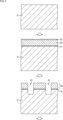
- 3A to 3C are diagrams illustrating first to third steps of a manufacturing method for an image sensor.
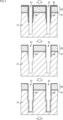
- 11A to 11C are diagrams illustrating fourth to sixth steps of the manufacturing method of the image sensor.
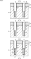
- 7A to 7C are diagrams illustrating seventh to ninth steps of the manufacturing method of the image sensor.
- 10A to 12B are diagrams illustrating tenth to twelfth steps of a manufacturing method of an image sensor.
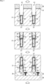
- 13A to 15C are diagrams illustrating thirteenth to fifteenth steps of the manufacturing method of an image sensor.
- 16A to 18C are diagrams illustrating the 16th to 18th steps of the manufacturing method of an image sensor.
- FIG. 1 is a block diagram showing an example of the configuration of an imaging apparatus.
- FIG. 1 is a diagram showing an example of use of an image
- FIG. 1 is a diagram showing an example of the configuration of an embodiment of an imaging element to which the present technology is applied.
- the imaging element 11 is configured with a pixel region in which a plurality of pixels 21 are arranged in an array, and a peripheral region that is provided to surround the periphery of the pixel region.
- the imaging element 11 is also configured with a wiring layer 23 laminated on a surface (hereinafter referred to as the FEOL surface) of a sensor layer 22 in which a photoelectric conversion unit PD is provided for each pixel 21, and an on-chip lens layer 24 laminated on a back surface (hereinafter referred to as the REOL surface) of the sensor layer 22.
- the REOL surface is the first surface that is the light incident surface of the semiconductor substrate 31, and the FEOL surface is the second surface of the semiconductor substrate 31 that is opposite to the REOL surface.
- the sensor layer 22 is configured, for example, by forming photoelectric conversion units PD by ion-implanting N-type impurities into a semiconductor substrate 31 in which a P-type well is provided.
- Pixel isolation units 32 are provided between the photoelectric conversion units PD in the semiconductor substrate 31 so as to surround each photoelectric conversion unit PD and separate the pixels 21 from each other.
- Isolation units 33 are also provided in the semiconductor substrate 31 that forms the peripheral region of the sensor layer 22. Note that in the semiconductor substrate 31 shown in FIG. 1, the narrow-pitch hatched regions that are in contact with the side surfaces of the pixel isolation units 32 and isolation units 33 indicate that the side surfaces of the trenches are doped by adding impurities such as boron (B).
- the wiring layer 23 is configured by providing, within an insulating film 36, a gate electrode 34 of a transistor that drives the pixel 21, a contact electrode 35 electrically connected to the gate electrode 34, wiring (not shown), and the like.
- a contact electrode 37 electrically connected to the polysilicon layer 44A of the separation section 33 is provided within the insulating film 36.
- the on-chip lens layer 24 is laminated on the REOL surface of the semiconductor substrate 31 via a high dielectric constant film 46 and a second insulating layer 47, and the pixel region is configured with a microlens 38 that focuses light for each pixel 21.
- a transparent material that constitutes the microlens 38 is provided flatly in the peripheral region of the on-chip lens layer 24.
- the pixel separation section 32 is configured by providing a connection layer 41 made of a semiconductor in the middle of a trench provided to penetrate the semiconductor substrate 31, connecting the semiconductor substrates 31 on both sides of the trench.
- the connection layer 41 is formed of a semiconductor (single crystal silicon of the same P type as the well of the pixel 21) epitaxially grown from both the connection portion 42a with one semiconductor substrate 31 separated by the pixel separation section 32 and the connection portion 42b with the other semiconductor substrate 31 separated by the pixel separation section 32, and electrically connects the connection portion 42a and the connection portion 42b.
- connection layer 41 is not limited to being formed by epitaxial growth, as long as it can electrically connect the well of one pixel 21 to the well of the other pixel 21 and can be formed of a material that can be formed in a self-aligned manner using the connection portion 42a and the connection portion 42b.
- the pixel separation section 32 is configured such that an insulating film 43 is provided to cover the FEOL surface side of the connection layer 41 and both side surfaces of the trench that are closer to the FEOL surface than the connection parts 42a and 42b, and a polysilicon layer 44 and a first insulating layer 45 are embedded inside the trench via the insulating film 43. That is, the polysilicon layer 44 is provided on the FEOL surface side of the connection layer 41 via the insulating film 43, and the first insulating layer 45 is provided on the FEOL surface side of the polysilicon layer 44. As shown enlarged on the left side of FIG.
- the insulating film 43 is formed such that an insulating film 43a is provided between the connection layer 41 and the polysilicon layer 44, insulating films 43b and 43c are provided on both side surfaces of the connection layer 41, and insulating films 43c and 43d are provided on both side surfaces of the polysilicon layer 44.
- the pixel separation section 32 is also configured such that a high dielectric constant film 46 is provided to cover the REOL surface side of the connection layer 41 and both side surfaces of the trench that are closer to the REOL surface than the connection layer 41, and a second insulating layer 47 is embedded inside the trench via the high dielectric constant film 46. Furthermore, the high dielectric constant film 46 is laminated on the REOL surface of the semiconductor substrate 31, and the second insulating layer 47 is laminated on the REOL surface of the semiconductor substrate 31 via the high dielectric constant film 46.
- the pixel separation section 32 has a laminated structure in which the region where the connection layer 41 is provided is the second layer, the REOL surface side of the connection layer 41 is the first layer, and the FEOL surface side of the connection layer 41 is the third layer.
- the pixel separation section 32 is formed in a shape in which a step is provided in the width of the connection layer 41 in the second layer, and the pixel separation section 32 is formed in a shape in which the width is different on the first layer side and the third layer side in a cross-sectional view.
- the pixel separation section 32 is formed so that the cross-sectional shape is convex, so that the REOL surface side of the connection layer 41 is narrow and the FEOL surface side of the connection layer 41 is wide. Accordingly, the pixel separation section 32 is configured so that the width D1 of the first layer on the REOL surface side is narrow, and the width D3 of the third layer on the FEOL surface side is wide.
- the semiconductor substrate 31 can be formed to a thickness of up to 6 ⁇ m, and the pixel separation section 32 can be formed so that the first layer is provided at a depth from the FEOL surface in the range of 0.2 to 6 ⁇ m, the second layer is provided at a position at a depth from the FEOL surface in the range of 0.1 to 6 ⁇ m with a width of 0.1 ⁇ m or more, and the third layer is provided at a depth from the FEOL surface in the range of 0.1 to 1 ⁇ m.
- the separation section 33 is configured similarly to the pixel separation section 32, but differs from the pixel separation section 32 in that a polysilicon layer 44A is embedded in the region in which the first insulating layer 45 and the polysilicon layer 44 are embedded in the pixel separation section 32.
- a contact electrode 37 is connected to the polysilicon layer 44A, and a bias voltage can be applied via the contact electrode 37.
- the image sensor 11 is constructed, and the pixel separation section 32 can be formed with greater precision by forming the connection layer 41 from a material that can be formed in a self-aligned manner (e.g., single crystal silicon formed by epitaxial growth) based on the connection portion 42a and the connection portion 42b on both sides of the middle of the trench that is provided to penetrate the silicon substrate, which is the semiconductor substrate 31.
- a self-aligned manner e.g., single crystal silicon formed by epitaxial growth
- the connection layer 41 is formed in a self-aligned manner at a predetermined position in the in-plane direction and depth direction of the semiconductor substrate 31 by utilizing the step portion (see the second step in Figure 5) formed in the middle of the trench.
- the image sensor 11 can avoid the occurrence of misalignment and variation that would adversely affect the pixel characteristics, and as a result, the characteristics of the pixel 21 can be improved.
- the imaging element 11 has a polysilicon layer 44 on a portion of the FEOL surface side, and a second insulating layer 47 is embedded on the REOL surface side via a high dielectric constant film 46.
- This configuration makes it possible to avoid a decrease in quantum efficiency Qe due to light absorption and suppress deterioration of dark current, compared to a configuration in which polysilicon is embedded in the entire separation section, for example.
- the image sensor 11 can be configured to eliminate the need for well taps that were previously provided to connect those wells.
- FIG. 2 shows an example of a planar configuration of four pixels 21 arranged in a 2 ⁇ 2 array.
- the pixels 21 can be configured to have a rectangular shape in a plan view.
- the pixel separator 32 is provided to surround each pixel 21.
- the pixels 21 can be configured to have a rectangular shape in which two opposing sides (the upper side and the lower side in the illustrated example) have inwardly directed notches in a plan view.
- the pixel separators 32 are provided so as to surround each pixel 21, and are also provided in the notches of each pixel 21.
- pixel 21 may have a planar shape other than the shape shown in FIG. 2.
- a semiconductor substrate 31 is prepared that has been processed to a predetermined thickness (e.g., 6 ⁇ m or more).
- a SiN film 51, a SiO layer 52, and a polysilicon film 53 used as a hard mask are laminated on the surface of the semiconductor substrate 31.
- the SiN film 51 and the SiO layer 52 are processed so that the area where the pixel separation portion 32 is to be formed is opened, and the semiconductor substrate 31 is shallowly excavated using the SiN film 51 and the SiO layer 52 as a hard mask to form a trench 61.
- the depth of the trench 61 is set according to the distance from the FEOL surface of the area where the first insulating layer 45 shown in FIG. 1 is embedded.
- a SiN film 54 is formed. As shown in the figure, the SiN film 54 is provided so as to cover the bottom and side surfaces of the trench 61 and the surface of the SiO layer 52.
- the SiN film 54 on the bottom surface of the trench 61 is removed, and the semiconductor substrate 31 on the bottom surface is dug in to deepen the depth of the trench 61.
- the depth of the trench 61 is set according to the distance from the FEOL surface to the region in which the polysilicon layer 44 shown in FIG. 1 is embedded.
- a SiO film 55 is formed. As shown in the figure, the SiO film 55 is provided so as to cover the bottom and side surfaces of the trench 61, as well as the surface of the SiO layer 52 via the SiN film 54.
- the SiO film 55 on the bottom surface of the trench 61 is removed, and the semiconductor substrate 31 on the bottom surface is dug in to deepen the depth of the trench 61.
- the depth of the trench 61 is set to be greater than or equal to the thickness of the sensor layer 22 shown in FIG. 1.
- the SiO film 55 is removed. This forms a stepped portion with a step in the middle of the trench 61.
- the side of the trench 61 is doped by, for example, ion implantation of boron into the side of the semiconductor substrate 31 in the region of the side of the trench 61 where the SiN film 54 is not formed.
- a SiO film 56 is formed. As shown in the figure, the SiO film 56 is provided to cover the bottom and side surfaces of the trench 61 and to cover the surface of the SiO layer 52 via the SiN film 54.
- an etch-back is performed on the SiO film 56.
- This removes the SiO film 56 that was stacked on the step formed in the middle of the trench 61, exposing the semiconductor substrate 31 at the portions that will become the connection portions 42a and 42b (see FIG. 1).
- the SiO film 56 that was stacked on the bottom surface of the trench 61 is removed to expose the semiconductor substrate 31, and the SiO film 56 that was stacked on the surface of the SiO layer 52 is also removed.
- a semiconductor is epitaxially grown from the step portion and bottom surface of the trench 61 where the semiconductor substrate 31 is exposed.
- a connection layer 41 is formed in the step portion formed in the middle of the trench 61, and a bottom layer 57 is formed on the bottom surface of the trench 61.
- the space sandwiched between the connection layer 41 and the bottom layer 57 becomes a cavity 62 that is not filled with anything.
- the SiO film 56 in the area other than the cavity 62 is removed, and the SiN film 54 is removed.
- an insulating film 43 is formed on the side surface of the trench 61 and the surface of the connection layer 41, and a polysilicon layer 44 and a first insulating layer 45 are embedded inside the trench 61.
- the SiN film 51 and the SiO layer 52 used as a hard mask are removed.
- a wiring layer 23 is laminated on the front surface of the semiconductor substrate 31, and a logic substrate 25 having a logic circuit formed thereon is bonded via the wiring layer 23.
- the semiconductor substrate 31 is then inverted to carry out processes on the rear surface side.
- the semiconductor substrate 31 is thinned to the thickness of the sensor layer 22. This removes the bottom layer 57 and opens the back side of the cavity 62, thereby providing a trench 63.
- the SiO film 56 on the side of the trench 63 is removed, and then a high-dielectric film 46 is formed using, for example, aluminum oxide (AlO) or hafnium oxide (HfO). As shown in the figure, the high-dielectric film 46 is provided so as to cover the bottom and side of the trench 63, as well as the back surface of the semiconductor substrate 31.
- AlO aluminum oxide
- HfO hafnium oxide
- the second insulating layer 47 is formed. As shown in the figure, the second insulating layer 47 is embedded inside the trench 63 via the high dielectric constant film 46, and is provided so as to cover the back surface of the semiconductor substrate 31 via the high dielectric constant film 46.
- the sensor layer 22 can be formed in the pixel separation section 32.
- a step portion (see the second row in FIG. 5) formed in the middle of a trench 61 provided in the semiconductor substrate 31 can be used to form the connection layer 41 in a self-aligned manner at a predetermined position in the in-plane direction and depth direction of the semiconductor substrate 31 (see the third row in FIG. 6). This allows the pixel separation section 32 to be formed with high precision, thereby improving the characteristics of the pixel 21.
- the pixel separator 32 can be configured to have a metal film such as tungsten, aluminum, or silver deposited instead of the high dielectric constant film 46, or can be configured to have a metal such as tungsten or copper embedded instead of the polysilicon layer 44.
- the imaging element 11 as described above can be applied to various electronic devices, such as imaging systems such as digital still cameras and digital video cameras, mobile phones with imaging functions, and other devices with imaging functions.
- FIG. 9 is a block diagram showing an example of the configuration of an imaging device installed in an electronic device.
- the imaging device 101 is configured with an optical system 102, an imaging element 103, a signal processing circuit 104, a monitor 105, and a memory 106, and is capable of capturing still images and moving images.
- the optical system 102 is composed of one or more lenses, and guides image light (incident light) from a subject to the image sensor 103, forming an image on the light receiving surface (sensor section) of the image sensor 103.
- the imaging element 103 is the imaging element 11 described above. Electrons are accumulated in the imaging element 103 for a certain period of time according to the image formed on the light receiving surface via the optical system 102. Then, a signal according to the electrons accumulated in the imaging element 103 is supplied to the signal processing circuit 104.
- the signal processing circuit 104 performs various signal processing on the pixel signals output from the image sensor 103.
- the image (image data) obtained by performing the signal processing by the signal processing circuit 104 is supplied to the monitor 105 for display, or supplied to the memory 106 for storage (recording).
- the imaging device 101 configured in this manner, by applying the imaging element 11 described above, it is possible to capture images with higher image quality, for example.
- FIG. 10 is a diagram showing an example of using the above-mentioned image sensor (imaging element).
- the image sensor described above can be used in a variety of cases, such as sensing visible light, infrared light, ultraviolet light, X-rays, etc., as follows:
- - Devices that take images for viewing such as digital cameras and mobile devices with camera functions
- - Devices for traffic purposes such as in-vehicle sensors that take images of the front and rear of a car, the surroundings, and the interior of the car for safe driving such as automatic stopping and for recognizing the driver's state, surveillance cameras that monitor moving vehicles and roads, and distance measuring sensors that measure the distance between vehicles, etc.
- - Devices for home appliances such as TVs, refrigerators, and air conditioners that take images of users' gestures and operate devices in accordance with those gestures
- - Devices for medical and healthcare purposes such as endoscopes and devices that take images of blood vessels by receiving infrared light
- - Devices for security purposes such as surveillance cameras for crime prevention and cameras for person authentication
- - Devices for beauty purposes such as skin measuring devices that take images of the skin and microscopes that take images of the scalp
- - Devices for sports purposes such as action cameras and wearable cameras for sports purposes, etc.
- - Devices for agricultural purposes such as cameras
- the present technology can also be configured as follows. (1) a semiconductor substrate having a first surface serving as a light incident surface and a second surface opposite to the first surface; A first photoelectric conversion unit provided in the semiconductor substrate; A second photoelectric conversion unit provided adjacent to the first photoelectric conversion unit; a pixel separator provided between the first photoelectric conversion unit and the second photoelectric conversion unit, the pixel separation section has a laminated structure in which a first layer, a second layer, and a third layer are laminated in this order from the first surface side in a cross-sectional view, the second layer has a shape in which a width on the first layer side and a width on the third layer side are different in a cross-sectional view.
- the insulating film is provided between the second layer and the third layer, and on both side surfaces of the third layer;
- a high dielectric constant film is provided between the first layer and the second layer and on both side surfaces of the first layer;
- a semiconductor substrate having a first surface serving as a light incident surface and a second surface opposite to the first surface; A first photoelectric conversion unit provided in the semiconductor substrate; A second photoelectric conversion unit provided adjacent to the first photoelectric conversion unit; a pixel separator provided between the first photoelectric conversion unit and the second photoelectric conversion unit, the pixel separation section has a laminated structure in which a first layer, a second layer, and a third layer are laminated in this order from the first surface side in a cross-sectional view, the second layer has a shape having a different width on the first layer side and on the third layer side in a cross-sectional view, forming the second layer in a self-aligned manner at a predetermined position in an in-plane direction and a depth direction of the semiconductor substrate by utilizing a step portion formed in the middle of a trench provided in the semiconductor substrate.
- a semiconductor substrate having a first surface serving as a light incident surface and a second surface opposite to the first surface; A first photoelectric conversion unit provided in the semiconductor substrate; A second photoelectric conversion unit provided adjacent to the first photoelectric conversion unit; a pixel separation unit provided between the first photoelectric conversion unit and the second photoelectric conversion unit, the pixel separation section has a laminated structure in which a first layer, a second layer, and a third layer are laminated in this order from the first surface side in a cross-sectional view, the second layer has a shape in which a width differs between the first layer side and the third layer side in a cross-sectional view.
- 11 imaging element 21 pixel, 22 sensor layer, 23 wiring layer, 24 on-chip lens layer, 25 logic substrate, 31 semiconductor substrate, 32 pixel separation section, 33 separation section, 34 gate electrode, 35 contact electrode, 36 insulating film, 37 contact electrode, 38 microlens, 41 connection layer, 42 connection section, 43 insulating film, 44 polysilicon layer, 45 first insulating layer, 46 high dielectric constant film, 47 second insulating layer, 51 SiN film, 52 SiO layer, 53 polysilicon film, 54 SiN film, 55 and 56 SiO film, 57 bottom layer, 61 trench, 62 cavity, 63 trench
Landscapes
- Solid State Image Pick-Up Elements (AREA)
Abstract
Description
図1は、本技術を適用した撮像素子の一実施の形態の構成例を示す図である。
図3乃至図8を参照して、撮像素子11の製造方法のうち、画素分離部32を形成する工程について説明する。
上述したような撮像素子11は、例えば、デジタルスチルカメラやデジタルビデオカメラなどの撮像システム、撮像機能を備えた携帯電話機、または、撮像機能を備えた他の機器といった各種の電子機器に適用することができる。
図10は、上述のイメージセンサ(撮像素子)を使用する使用例を示す図である。
・自動停止等の安全運転や、運転者の状態の認識等のために、自動車の前方や後方、周囲、車内等を撮影する車載用センサ、走行車両や道路を監視する監視カメラ、車両間等の測距を行う測距センサ等の、交通の用に供される装置
・ユーザのジェスチャを撮影して、そのジェスチャに従った機器操作を行うために、TVや、冷蔵庫、エアーコンディショナ等の家電に供される装置
・内視鏡や、赤外光の受光による血管撮影を行う装置等の、医療やヘルスケアの用に供される装置
・防犯用途の監視カメラや、人物認証用途のカメラ等の、セキュリティの用に供される装置
・肌を撮影する肌測定器や、頭皮を撮影するマイクロスコープ等の、美容の用に供される装置
・スポーツ用途等向けのアクションカメラやウェアラブルカメラ等の、スポーツの用に供される装置
・畑や作物の状態を監視するためのカメラ等の、農業の用に供される装置
なお、本技術は以下のような構成も取ることができる。
(1)
光入射面となる第1面と、前記第1面とは反対側となる第2面とを有する半導体基板と、
前記半導体基板内に設けられた第1光電変換部と、
前記第1光電変換部に隣接して設けられた第2光電変換部と、
前記第1光電変換部と前記第2光電変換部との間に設けられた画素分離部と
を備え、
前記画素分離部は、断面視で前記第1面側から順に第1層、第2層、および第3層が積層された積層構造となっており、
前記第2層は、断面視で前記第1層側と前記第3層側とで幅が異なる形状である
固体撮像素子。
(2)
前記第2層は、前記半導体基板に設けられたトレンチの中間に形成される段差部を利用して、前記半導体基板の面内方向および深さ方向の所定位置に自己整合的に形成される
上記(1)に記載の固体撮像素子。
(3)
前記第2層は、前記半導体基板のウェルと同一の導電型の半導体によって構成され、
断面視で前記第2層の両側面には、前記半導体基板と電気的に接続される接続部が設けられる
上記(1)または(2)に記載の固体撮像素子。
(4)
前記第2層は、前記半導体基板であるシリコン基板に設けられたトレンチの中間において、そのトレンチの両側面にある前記接続部からエピタキシャル成長により形成される単結晶シリコンにより構成される
上記(3)に記載の固体撮像素子。
(5)
前記第2層は、前記第1層側が幅狭となり、かつ、前記第3層側が幅広となる断面形状となっており、その幅広となる個所の両側面に絶縁膜が設けられる
上記(1)から(4)までのいずれかに記載の固体撮像素子。
(6)
前記絶縁膜は、前記第2層と前記第3層との間にも設けられるとともに、前記第3層の両側面にも設けられ、
前記絶縁膜を介してポリシリコン層および第1の絶縁層が積層されて前記第3層が構成される
上記(5)に記載の固体撮像素子。
(7)
前記第1層と前記第2層との間、および、前記第1層の両側面に高誘電率膜が設けられ、
前記高誘電率膜を介して第2の絶縁層が積層されて前記第1層が構成される
上記(6)に記載の固体撮像素子。
(8)
前記画素分離部の側面となる前記半導体基板のうち、前記第1層および前記第2層の領域、並びに、前記第3層の前記ポリシリコン層が設けられている領域における側面が不純物によってドーピングされている
上記(7)に記載の固体撮像素子。
(9)
光入射面となる第1面と、前記第1面とは反対側となる第2面とを有する半導体基板と、
前記半導体基板内に設けられた第1光電変換部と、
前記第1光電変換部に隣接して設けられた第2光電変換部と、
前記第1光電変換部と前記第2光電変換部との間に設けられた画素分離部と
を備え、
前記画素分離部は、断面視で前記第1面側から順に第1層、第2層、および第3層が積層された積層構造となっており、
前記第2層は、断面視で前記第1層側と前記第3層側とで幅が異なる形状である
固体撮像素子の製造方法であって、
前記第2層を、前記半導体基板に設けられたトレンチの中間に形成される段差部を利用して、前記半導体基板の面内方向および深さ方向の所定位置に自己整合的に形成すること
を含む製造方法。
(10)
光入射面となる第1面と、前記第1面とは反対側となる第2面とを有する半導体基板と、
前記半導体基板内に設けられた第1光電変換部と、
前記第1光電変換部に隣接して設けられた第2光電変換部と、
前記第1光電変換部と前記第2光電変換部との間に設けられた画素分離部と
を有し、
前記画素分離部は、断面視で前記第1面側から順に第1層、第2層、および第3層が積層された積層構造となっており、
前記第2層は、断面視で前記第1層側と前記第3層側とで幅が異なる形状である
固体撮像素子を備える電子機器。
Claims (10)
- 光入射面となる第1面と、前記第1面とは反対側となる第2面とを有する半導体基板と、
前記半導体基板内に設けられた第1光電変換部と、
前記第1光電変換部に隣接して設けられた第2光電変換部と、
前記第1光電変換部と前記第2光電変換部との間に設けられた画素分離部と
を備え、
前記画素分離部は、断面視で前記第1面側から順に第1層、第2層、および第3層が積層された積層構造となっており、
前記第2層は、断面視で前記第1層側と前記第3層側とで幅が異なる形状である
固体撮像素子。 - 前記第2層は、前記半導体基板に設けられたトレンチの中間に形成される段差部を利用して、前記半導体基板の面内方向および深さ方向の所定位置に自己整合的に形成される
請求項1に記載の固体撮像素子。 - 前記第2層は、前記半導体基板のウェルと同一の導電型の半導体によって構成され、
断面視で前記第2層の両側面には、前記半導体基板と電気的に接続される接続部が設けられる
請求項1に記載の固体撮像素子。 - 前記第2層は、前記半導体基板であるシリコン基板に設けられたトレンチの中間において、そのトレンチの両側面にある前記接続部からエピタキシャル成長により形成される単結晶シリコンにより構成される
請求項3に記載の固体撮像素子。 - 前記第2層は、前記第1層側が幅狭となり、かつ、前記第3層側が幅広となる断面形状となっており、その幅広となる個所の両側面に絶縁膜が設けられる
請求項1に記載の固体撮像素子。 - 前記絶縁膜は、前記第2層と前記第3層との間にも設けられるとともに、前記第3層の両側面にも設けられ、
前記絶縁膜を介してポリシリコン層および第1の絶縁層が積層されて前記第3層が構成される
請求項5に記載の固体撮像素子。 - 前記第1層と前記第2層との間、および、前記第1層の両側面に高誘電率膜が設けられ、
前記高誘電率膜を介して第2の絶縁層が積層されて前記第1層が構成される
請求項6に記載の固体撮像素子。 - 前記画素分離部の側面となる前記半導体基板のうち、前記第1層および前記第2層の領域、並びに、前記第3層の前記ポリシリコン層が設けられている領域における側面が不純物によってドーピングされている
請求項7に記載の固体撮像素子。 - 光入射面となる第1面と、前記第1面とは反対側となる第2面とを有する半導体基板と、
前記半導体基板内に設けられた第1光電変換部と、
前記第1光電変換部に隣接して設けられた第2光電変換部と、
前記第1光電変換部と前記第2光電変換部との間に設けられた画素分離部と
を備え、
前記画素分離部は、断面視で前記第1面側から順に第1層、第2層、および第3層が積層された積層構造となっており、
前記第2層は、断面視で前記第1層側と前記第3層側とで幅が異なる形状である
固体撮像素子の製造方法であって、
前記第2層を、前記半導体基板に設けられたトレンチの中間に形成される段差部を利用して、前記半導体基板の面内方向および深さ方向の所定位置に自己整合的に形成すること
を含む製造方法。 - 光入射面となる第1面と、前記第1面とは反対側となる第2面とを有する半導体基板と、
前記半導体基板内に設けられた第1光電変換部と、
前記第1光電変換部に隣接して設けられた第2光電変換部と、
前記第1光電変換部と前記第2光電変換部との間に設けられた画素分離部と
を有し、
前記画素分離部は、断面視で前記第1面側から順に第1層、第2層、および第3層が積層された積層構造となっており、
前記第2層は、断面視で前記第1層側と前記第3層側とで幅が異なる形状である
固体撮像素子を備える電子機器。
Priority Applications (2)
| Application Number | Priority Date | Filing Date | Title |
|---|---|---|---|
| KR1020257027006A KR20250139828A (ko) | 2023-01-30 | 2024-01-18 | 고체 촬상 소자 및 제조 방법, 그리고 전자 기기 |
| CN202480005938.4A CN120435929A (zh) | 2023-01-30 | 2024-01-18 | 固体摄像元件、固体摄像元件制造方法及电子设备 |
Applications Claiming Priority (2)
| Application Number | Priority Date | Filing Date | Title |
|---|---|---|---|
| JP2023-012038 | 2023-01-30 | ||
| JP2023012038 | 2023-01-30 |
Publications (1)
| Publication Number | Publication Date |
|---|---|
| WO2024162013A1 true WO2024162013A1 (ja) | 2024-08-08 |
Family
ID=92146280
Family Applications (1)
| Application Number | Title | Priority Date | Filing Date |
|---|---|---|---|
| PCT/JP2024/001197 Ceased WO2024162013A1 (ja) | 2023-01-30 | 2024-01-18 | 固体撮像素子および製造方法、並びに電子機器 |
Country Status (3)
| Country | Link |
|---|---|
| KR (1) | KR20250139828A (ja) |
| CN (1) | CN120435929A (ja) |
| WO (1) | WO2024162013A1 (ja) |
Citations (4)
| Publication number | Priority date | Publication date | Assignee | Title |
|---|---|---|---|---|
| US20170170229A1 (en) * | 2015-12-09 | 2017-06-15 | Samsung Electronics Co., Ltd. | Image sensor and method of manufacturing the same |
| JP2019140219A (ja) * | 2018-02-09 | 2019-08-22 | ソニーセミコンダクタソリューションズ株式会社 | 半導体装置および半導体装置の製造方法 |
| JP2020188267A (ja) * | 2020-07-14 | 2020-11-19 | キヤノン株式会社 | 撮像装置 |
| JP2022112240A (ja) * | 2021-01-21 | 2022-08-02 | ソニーセミコンダクタソリューションズ株式会社 | 光検出装置及び電子機器 |
Family Cites Families (1)
| Publication number | Priority date | Publication date | Assignee | Title |
|---|---|---|---|---|
| US10700114B2 (en) | 2016-04-25 | 2020-06-30 | Sony Corporation | Solid-state imaging element, method for manufacturing the same, and electronic apparatus |
-
2024
- 2024-01-18 KR KR1020257027006A patent/KR20250139828A/ko active Pending
- 2024-01-18 CN CN202480005938.4A patent/CN120435929A/zh active Pending
- 2024-01-18 WO PCT/JP2024/001197 patent/WO2024162013A1/ja not_active Ceased
Patent Citations (4)
| Publication number | Priority date | Publication date | Assignee | Title |
|---|---|---|---|---|
| US20170170229A1 (en) * | 2015-12-09 | 2017-06-15 | Samsung Electronics Co., Ltd. | Image sensor and method of manufacturing the same |
| JP2019140219A (ja) * | 2018-02-09 | 2019-08-22 | ソニーセミコンダクタソリューションズ株式会社 | 半導体装置および半導体装置の製造方法 |
| JP2020188267A (ja) * | 2020-07-14 | 2020-11-19 | キヤノン株式会社 | 撮像装置 |
| JP2022112240A (ja) * | 2021-01-21 | 2022-08-02 | ソニーセミコンダクタソリューションズ株式会社 | 光検出装置及び電子機器 |
Also Published As
| Publication number | Publication date |
|---|---|
| KR20250139828A (ko) | 2025-09-23 |
| CN120435929A (zh) | 2025-08-05 |
Similar Documents
| Publication | Publication Date | Title |
|---|---|---|
| KR102536429B1 (ko) | 촬상 소자 및 그 제조 방법 및 전자 기기 | |
| US12538591B2 (en) | Imaging device | |
| JP7006268B2 (ja) | 撮像素子、電子機器、並びに、製造装置および方法 | |
| KR102880492B1 (ko) | 고체 이미지 센서, 및 전자 장치 | |
| CN109461747B (zh) | 成像器件及电子装置 | |
| JP7403993B2 (ja) | 固体撮像装置およびその製造方法、並びに電子機器 | |
| US10490586B2 (en) | Solid-state imaging device with light shielding films, method of manufacturing the same, and electronic apparatus | |
| JP2020043265A (ja) | 光電変換装置および機器 | |
| WO2016152577A1 (ja) | 固体撮像装置および電子機器 | |
| JP2021027276A (ja) | 光電変換装置および機器 | |
| JP7479801B2 (ja) | 撮像素子、製造方法、および電子機器 | |
| JP2016167530A (ja) | 固体撮像装置及びその製造方法、並びに電子機器 | |
| US12356738B2 (en) | Semiconductor apparatus and device | |
| US10531020B2 (en) | Solid-state image pickup device, manufacturing method therefor, and electronic apparatus | |
| CN115956285A (zh) | 半导体装置、成像装置和电子设备 | |
| WO2024162013A1 (ja) | 固体撮像素子および製造方法、並びに電子機器 | |
| US11948953B2 (en) | Solid-state imaging device and electronic apparatus | |
| US20210159260A1 (en) | Photoelectric conversion apparatus, method for manufacturing photoelectric conversion apparatus, and equipment | |
| US20250311525A1 (en) | Imaging Element and Method Of Manufacturing the Same, and Electronic Apparatus | |
| WO2023153300A1 (ja) | 固体撮像素子および製造方法、並びに電子機器 | |
| JP7022174B2 (ja) | 固体撮像素子、および電子装置 | |
| WO2025109913A1 (ja) | 半導体装置および電子機器 | |
| JP2021015997A (ja) | 光電変換装置およびカメラ |
Legal Events
| Date | Code | Title | Description |
|---|---|---|---|
| 121 | Ep: the epo has been informed by wipo that ep was designated in this application |
Ref document number: 24749967 Country of ref document: EP Kind code of ref document: A1 |
|
| WWE | Wipo information: entry into national phase |
Ref document number: 202480005938.4 Country of ref document: CN |
|
| WWP | Wipo information: published in national office |
Ref document number: 202480005938.4 Country of ref document: CN |
|
| ENP | Entry into the national phase |
Ref document number: 1020257027006 Country of ref document: KR Free format text: ST27 STATUS EVENT CODE: A-0-1-A10-A15-NAP-PA0105 (AS PROVIDED BY THE NATIONAL OFFICE) |
|
| NENP | Non-entry into the national phase |
Ref country code: DE |
|
| 122 | Ep: pct application non-entry in european phase |
Ref document number: 24749967 Country of ref document: EP Kind code of ref document: A1 |
|
| NENP | Non-entry into the national phase |
Ref country code: JP |