WO2024162008A1 - 光電気配線基板および光電気配線基板の製造方法 - Google Patents
光電気配線基板および光電気配線基板の製造方法 Download PDFInfo
- Publication number
- WO2024162008A1 WO2024162008A1 PCT/JP2024/001153 JP2024001153W WO2024162008A1 WO 2024162008 A1 WO2024162008 A1 WO 2024162008A1 JP 2024001153 W JP2024001153 W JP 2024001153W WO 2024162008 A1 WO2024162008 A1 WO 2024162008A1
- Authority
- WO
- WIPO (PCT)
- Prior art keywords
- electrical wiring
- optical
- wiring board
- metal
- optical waveguide
- Prior art date
- Legal status (The legal status is an assumption and is not a legal conclusion. Google has not performed a legal analysis and makes no representation as to the accuracy of the status listed.)
- Ceased
Links
Images






Classifications
-
- G—PHYSICS
- G02—OPTICS
- G02B—OPTICAL ELEMENTS, SYSTEMS OR APPARATUS
- G02B6/00—Light guides; Structural details of arrangements comprising light guides and other optical elements, e.g. couplings
- G02B6/10—Light guides; Structural details of arrangements comprising light guides and other optical elements, e.g. couplings of the optical waveguide type
- G02B6/12—Light guides; Structural details of arrangements comprising light guides and other optical elements, e.g. couplings of the optical waveguide type of the integrated circuit kind
- G02B6/122—Basic optical elements, e.g. light-guiding paths
-
- G—PHYSICS
- G02—OPTICS
- G02B—OPTICAL ELEMENTS, SYSTEMS OR APPARATUS
- G02B6/00—Light guides; Structural details of arrangements comprising light guides and other optical elements, e.g. couplings
- G02B6/10—Light guides; Structural details of arrangements comprising light guides and other optical elements, e.g. couplings of the optical waveguide type
- G02B6/12—Light guides; Structural details of arrangements comprising light guides and other optical elements, e.g. couplings of the optical waveguide type of the integrated circuit kind
- G02B6/13—Integrated optical circuits characterised by the manufacturing method
- G02B6/132—Integrated optical circuits characterised by the manufacturing method by deposition of thin films
Definitions
- the disclosed embodiments relate to an optical-electrical wiring board and a method for manufacturing an optical-electrical wiring board.
- optical-electrical wiring boards have been disclosed in which optical waveguide cores and electrical wiring are arranged on the same layer for the purpose of parallel transmission of optical signals and electrical signals (see, for example, Patent Document 1).
- the optical-electrical wiring board includes an optical waveguide core for transmitting an optical signal, electrical wiring for transmitting an electrical signal, and a metal portion located between the optical waveguide core and the electrical wiring that are adjacent to each other.
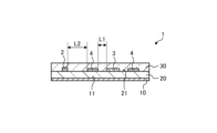
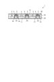
- FIG. 1 is a cross-sectional view showing an example of a configuration of an optical-electrical wiring board according to an embodiment.
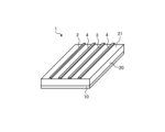
- FIG. 2 is a perspective view showing an example of a configuration of an optical-electrical wiring board according to the embodiment.
- FIG. 3 is a cross-sectional view showing an example of the configuration of an optical-electrical wiring board according to another embodiment 1.
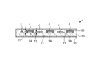
- FIG. 4 is a cross-sectional view showing an example of the configuration of an optical-electrical wiring board according to another embodiment 2.
- FIG. 5 is a cross-sectional view showing an example of the configuration of an optical-electrical wiring board according to another embodiment 3.
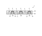
- FIG. 6 is a cross-sectional view showing an example of the configuration of an optical-electrical wiring board according to another embodiment 4.
- FIG. 7 is a cross-sectional view showing an example of the configuration of an optical-electrical wiring board according to another embodiment 5.
- FIG. 8 is a cross-sectional view showing an example of the configuration of an optical-electrical wiring board according to another embodiment 6.
- FIG. 9 is a cross-sectional view showing an example of the configuration of an optical-electrical wiring board according to another embodiment 7.
- FIG. 10 is a diagram for explaining a manufacturing process of an optical-electrical wiring board according to another embodiment 4.
- FIG. FIG. 11 is a diagram for explaining a manufacturing process of an optical-electrical wiring board according to another embodiment 7.
- FIG. 10 is a diagram for explaining a manufacturing process of an optical-electrical wiring board according to another embodiment 4.
- optical-electrical wiring boards have been disclosed in which optical waveguide cores and electrical wiring are arranged on the same layer for the purpose of parallel transmission of optical signals and electrical signals.
- Fig. 1 is a cross-sectional view showing an example of the configuration of an opto-electrical wiring board 1 according to an embodiment
- Fig. 2 is a perspective view showing an example of the configuration of an opto-electrical wiring board 1 according to an embodiment.
- the cladding layer 30 shown in Fig. 1 is omitted in Fig. 2.
- the optical-electrical wiring board 1 includes a metal layer 10, a cladding layer 20, and a cladding layer 30.
- the cladding layer 30 is an example of another cladding layer.
- the metal layer 10 is located along one of the main surfaces of a flat substrate (not shown).
- the metal layer 10 is located, for example, on the main surface of the substrate.
- the metal layer 10 is connected, for example, to a ground potential.
- the metal layer 10 is made of a metal material whose main component is, for example, copper, silver, aluminum, platinum, titanium, palladium, zinc, or chromium.
- the cladding layer 20 is located on the surface 11 of the metal layer 10.
- the cladding layer 20 is located so as to cover all or part of the metal layer 10.
- the cladding layer 30 is located on the surface 21 of the cladding layer 20.
- the cladding layer 30 is located so as to cover all or part of the cladding layer 20.
- the cladding layer 20 may be referred to as the first cladding layer 20
- the cladding layer 30 may be referred to as the second cladding layer 30.
- the cladding layers 20, 30 are made of a material that has a lower refractive index than the optical waveguide core 2 described below.
- the refractive index of the cladding layers 20, 30 is set, for example, in the range of 1.45 to 1.8.
- epoxy resin, polyimide resin, phenolic resin, or acrylic resin can be used for the cladding layers 20, 30.
- the optical-electrical wiring board 1 further includes an optical waveguide core 2, electrical wiring 3, and a metal portion 4.
- the optical waveguide core 2, electrical wiring 3, and metal portion 4 are located, for example, on the surface 21 of the cladding layer 20.
- the cladding layer 20 is a flat structure having a predetermined thickness and area
- the optical waveguide core 2, the electrical wiring 3, and the metal part 4 may have portions arranged at a predetermined interval in one direction on the cladding layer 20.
- the optical waveguide core 2, the electrical wiring 3, and the metal part 4 may have portions arranged in a substantially parallel manner on the cladding layer 20 in one direction, and in particular in a parallel manner.
- the optical waveguide core 2 is formed in a predetermined pattern on the surface 21 of the cladding layer 20. Also, as shown in FIG. 1, the optical waveguide core 2 is covered with the cladding layer 30. The optical waveguide core 2 has a higher refractive index than the cladding layers 20 and 30.
- the light that enters the optical waveguide core 2 travels through the optical waveguide core 2 while repeatedly being reflected at the interface between the optical waveguide core 2 and the cladding layer 20, and at the interface between the optical waveguide core 2 and the cladding layer 30.
- the optical waveguide core 2 has the function of transmitting optical signals in the opto-electrical wiring board 1.
- the refractive index of the optical waveguide core 2 is set, for example, in the range of 1.5 to 1.85.
- the refractive index of the optical waveguide core 2 may be, for example, 1% to 3% greater than the refractive index of the cladding layers 20, 30.
- epoxy resin or the like may be used for the optical waveguide core 2.
- the electrical wiring 3 is formed in a predetermined pattern on the surface 21 of the cladding layer 20. Also, as shown in FIG. 1, the electrical wiring 3 is covered with the cladding layer 30. The electrical wiring 3 has the function of transmitting electrical signals in the optical-electrical wiring board 1.
- the electrical wiring 3 is made of a metal material whose main component is, for example, copper, silver, aluminum, platinum, titanium, palladium, zinc, or chromium.
- a metal portion 4 is located between adjacent optical waveguide cores 2 and electrical wiring 3.
- This metal portion 4 is made of a metal material whose main component is, for example, copper, silver, aluminum, platinum, titanium, palladium, zinc, or chromium.
- the noise radiated toward the optical waveguide core 2 is suppressed by the metal part 4. That is, in the embodiment, it is possible to reduce the transmission of noise radiated from the electrical wiring 3 to the optical waveguide core 2.
- the optical noise radiated toward the electrical wiring 3 is blocked by the metal part 4. That is, in the embodiment, it is possible to reduce the transmission of the optical noise radiated from the optical waveguide core 2 to the electrical wiring 3.
- the metal part 4 may be connected to a ground potential. This allows the metal part 4 to efficiently suppress noise radiated from the electrical wiring 3 toward the optical waveguide core 2. Therefore, according to the embodiment, it is possible to further reduce signal interference between the optical waveguide core 2 and the electrical wiring 3.
- the metal portion 4 may be located between adjacent optical waveguide cores 2. This makes it possible to reduce signal interference between adjacent optical waveguide cores 2.
- the metal portion 4 may be located between adjacent electrical wirings 3. This can reduce signal interference between adjacent electrical wirings 3. Note that, when the optical waveguide core 2, electrical wirings 3, and metal portion 4 are arranged on the upper surface of the cladding layer 20 as shown in FIG. 1, they may be arranged at the same height from the metal layer 10 via the cladding layer 20.
- Fig. 3 is a cross-sectional view showing an example of the configuration of an opto-electrical wiring board 1 according to another embodiment 1. As shown in Fig. 3, in the opto-electrical wiring board 1 according to another embodiment 1, the position of the metal part 4 is different from that of the above-mentioned embodiment.
- the distance L1 between the metal part 4 and the electrical wiring 3 may be shorter than the distance L2 between the metal part 4 and the optical waveguide core 2. This allows the noise radiated from the electrical wiring 3 toward the optical waveguide core 2 to be effectively suppressed by the metal part 4 adjacent to the electrical wiring 3.
- FIG. 4 is a cross-sectional view showing an example of the configuration of an optical-electrical wiring board 1 according to another embodiment 2. As shown in FIG. 4, in the optical-electrical wiring board 1 according to another embodiment 2, the configuration of the metal part 4 differs from that of the above embodiment.
- the thickness T1 of the metal part 4 may be greater than the thickness T2 of the electrical wiring 3. This allows the noise radiated from the electrical wiring 3 toward the optical waveguide core 2 to be effectively suppressed by the metal part 4, which has a large dimension in the height direction.
- the optical-electrical wiring board 1 may have a structure in which the thickness T1 of the metal part 4 is thicker than the thickness T2 of the electrical wiring 3 in some places.
- the optical-electrical wiring board 1 may also have a structure in which the thickness T1 of the metal part 4 is thicker than the thickness T2 of the electrical wiring 3 in multiple places.
- the optical noise radiated from the optical waveguide core 2 toward the electrical wiring 3 can be effectively shielded by the metal part 4, which has a large dimension in the height direction. Therefore, according to the second alternative embodiment, the signal interference between the optical waveguide core 2 and the electrical wiring 3 can be further reduced.
- FIG. 5 is a cross-sectional view showing an example of the configuration of an optical-electrical wiring board 1 according to another embodiment 3. As shown in FIG. 5, in the optical-electrical wiring board 1 according to another embodiment 3, the configuration of the metal part 4 differs from that of the above-described another embodiment 2.
- the thickness T1 of the metal part 4 may be thicker than the thickness T2 of the electrical wiring 3 and may be longer than the width W of the metal part 4 in a cross-sectional view. That is, in another embodiment 3, the shape of the metal part 4 may be wall-like.
- the wall-shaped metal portion 4 may be arranged on the cladding layer 20 so as to be aligned along the direction in which the optical waveguide core 2 and the electrical wiring 3 extend.
- the wall-shaped metal portion 4 is arranged on the cladding layer 20 so as to be parallel to at least one of the optical waveguide core 2 and the electrical wiring 3.
- the portion of the metal part 4 that is parallel to at least one of the optical waveguide core 2 and the electrical wiring 3 on the cladding layer 20 may be the entire area of the metal part 4, the optical waveguide core 2, and the electrical wiring 3 provided on the optical-electrical wiring board 1, or may be partial.
- the metal part 4 may not be parallel near this curved portion, but may have a structure close to parallel.
- the metal part 4 be arranged parallel to them.
- the noise radiated from the electrical wiring 3 toward the optical waveguide core 2 can be effectively suppressed by the metal part 4, which has a larger dimension in the height direction.
- the metal part 4 which has a large dimension in the height direction, can effectively block the optical noise radiated from the optical waveguide core 2 toward the electrical wiring 3. Therefore, according to another embodiment 3, the signal interference between the optical waveguide core 2 and the electrical wiring 3 can be further reduced.
- the metal portion 4 in a wall shape by forming the metal portion 4 in a wall shape, the area occupied by the metal portion 4 in the optical-electrical wiring board 1 can be reduced, thereby increasing the design freedom of the optical-electrical wiring board 1.
- FIG. 6 is a cross-sectional view showing an example of the configuration of an optical-electrical wiring board 1 according to another embodiment 4. As shown in FIG. 6, in the optical-electrical wiring board 1 according to another embodiment 4, the configuration of the metal part 4 differs from that of the above embodiment.
- the metal part 4 may be inverted U-shaped in cross section.
- the metal part 4 may be positioned so as to cover the upper and side surfaces of the dummy core 2A.
- This dummy core 2A is made of the same material as the optical waveguide core 2, but unlike the optical waveguide core 2, it is a part that does not transmit optical signals.
- the inverted U-shape refers to the position of the open part of the U-shaped metal part 4 when viewed with the metal layer 10 side facing the ground (-Z direction) and the opposite side facing the sky (+Z direction) in Figure 6. This is used to conveniently show that the open part of the metal part 4 faces the metal layer 10 and clad layer 20.
- U-shaped does not only mean that the opening is curved like the letter U, but also includes the metal portion 4 where the portion located on the top surface of the dummy core 2A has a linear shape (a flat shape when the depth is taken into account) as shown in Figure 6.
- the thickness T1 of the metal part 4 can be made thicker than the thickness T2 of the electrical wiring 3. This makes it possible to effectively suppress noise radiated from the electrical wiring 3 toward the optical waveguide core 2 by the inverted U-shaped metal part 4, which has a large dimension in the height direction.
- the optical noise radiated from the optical waveguide core 2 toward the electrical wiring 3 can be effectively shielded by the inverted U-shaped metal part 4, which has a large dimension in the height direction. Therefore, according to another embodiment 4, the signal interference between the optical waveguide core 2 and the electrical wiring 3 can be further reduced.
- FIG. 7 is a cross-sectional view showing an example of the configuration of an optical-electrical wiring board 1 according to another embodiment 5. As shown in FIG. 7, in the optical-electrical wiring board 1 according to another embodiment 5, the configuration of the metal part 4 differs from that of the above-described another embodiment 4.
- the extension portion 4a that extends downward in the inverted U-shaped metal portion 4 may extend from the surface 21 of the cladding layer 20 to the inside of the cladding layer 20. This allows the noise radiated from the electrical wiring 3 toward the optical waveguide core 2 to be effectively suppressed by the inverted U-shaped metal portion 4, which has a large dimension in the height direction.
- the optical noise radiated from the optical waveguide core 2 toward the electrical wiring 3 can be effectively shielded by the inverted U-shaped metal part 4, which has a large dimension in the height direction. Therefore, according to another embodiment 5, the signal interference between the optical waveguide core 2 and the electrical wiring 3 can be further reduced.
- FIG. 8 is a cross-sectional view showing an example of the configuration of an optical-electrical wiring board 1 according to another embodiment 6. As shown in FIG. 8, in the optical-electrical wiring board 1 according to another embodiment 6, the configuration of the metal part 4 differs from that of the above-described other embodiments 4 and 5.
- the extension portion 4a that extends downward in the inverted U-shaped metal portion 4 may extend through the cladding layer 20 to the metal layer 10. This allows the noise radiated from the electrical wiring 3 toward the optical waveguide core 2 to be effectively suppressed by the inverted U-shaped metal portion 4, which has a large dimension in the height direction.
- the optical noise radiated from the optical waveguide core 2 toward the electrical wiring 3 can be effectively shielded by the inverted U-shaped metal part 4, which has a large dimension in the height direction. Therefore, according to another embodiment 6, the signal interference between the optical waveguide core 2 and the electrical wiring 3 can be further reduced.
- the metal layer 10, which is connected to the ground potential, and the metal portion 4 are electrically connected at the extension portion 4a, so that the metal portion 4 can be stabilized at the ground potential. This can improve the transmission quality of the electrical signal in the electrical wiring 3.
- FIG. 9 is a cross-sectional view showing an example of the configuration of an optical-electrical wiring board 1 according to another embodiment 7. As shown in FIG. 9, in the optical-electrical wiring board 1 according to another embodiment 7, the configuration around the metal portion 4 differs from that of the above-mentioned another embodiment 6.
- a metal layer 40 may be located on the surface 31 of the cladding layer 30.
- a metal layer 40 is an example of another metal layer.
- the metal layer 40 is connected to, for example, a ground potential.
- the metal layer 40 is made of a metal material whose main component is, for example, copper, silver, aluminum, platinum, titanium, palladium, zinc, or chromium.
- the metal part 4 may be connected to the metal layer 40 through the via 5.
- the metal layer 40 which is connected to the ground potential, and the metal part 4 are electrically connected through the via 5, so that the metal part 4 can be further stabilized at the ground potential.
- the transmission quality of the electrical signal in the electrical wiring 3 can be further improved.
- Fig. 10 is a diagram for explaining the manufacturing process of the optical-electrical wiring board 1 according to Alternative Embodiment 4.
- a metal layer 10 and a cladding layer 20 are laminated in this order along the main surface of a substrate (not shown).
- the metal layer 10 is formed by a known dry method (e.g., chemical vapor deposition (CVD), physical vapor deposition (PVD), etc.) or a known wet method (e.g., plating, etc.).
- the cladding layer 20 is formed, for example, by applying a resin having a predetermined refractive index to the surface 11 of the metal layer 10 to a predetermined thickness, and then curing the resin with heat, light, or the like.
- the optical waveguide core 2 and the dummy core 2A are formed on the surface 21 of the cladding layer 20.
- the optical waveguide core 2 and the dummy core 2A are formed in the same process.
- the optical waveguide core 2 and dummy core 2A are formed by applying a resin having a predetermined refractive index to a predetermined thickness on the surface 11 of the metal layer 10, hardening the resin with heat or light, and then patterning the hardened resin into a predetermined planar shape using a known method.
- the manufacturing process of the optical-electrical wiring board 1 can be simplified, and the manufacturing cost of the optical-electrical wiring board 1 can be reduced.
- electrical wiring 3 is formed on the surface 21 of the cladding layer 20, and metal parts 4 are formed on the upper and side surfaces of the dummy core 2A.
- the electrical wiring 3 and metal parts 4 are formed in the same process.
- a resist film is selectively formed by a known method in locations other than where the electrical wiring 3 and metal portion 4 are to be formed.
- a metal film including the electrical wiring 3 and metal portion 4 is formed on the surface of the intermediate body during the manufacturing process by a plating process or the like, and finally the resist film is peeled off by a known method to form the electrical wiring 3 and metal portion 4.
- the same process refers to a process in which the metal film that will become the electrical wiring 3 and the metal film that will become the metal portion 4 are deposited simultaneously in one plating process.
- depositing simultaneously can also be expressed as depositing at the same time.
- the manufacturing process of the optical-electrical wiring board 1 can be simplified, and the manufacturing cost of the optical-electrical wiring board 1 can be reduced.
- the thickness T1 (see FIG. 6) of the metal portion 4, which is formed in the same process as the electrical wiring 3, can be easily made thicker than the thickness T1 (see FIG. 6) of the electrical wiring 3.
- a cladding layer 30 is formed on the surface 21 of the cladding layer 20 so as to cover the optical waveguide core 2, the electrical wiring 3, and the metal portion 4.
- the cladding layer 30 is formed, for example, by applying a resin having a predetermined refractive index to the surface 21 of the cladding layer 20 to a predetermined thickness, and then curing the resin by treating it with heat, light, or the like.
- the formation of the cladding layer 30 completes the manufacturing process for the optical-electrical wiring board 1 according to another embodiment 4.
- FIG. 11 is a diagram for explaining the manufacturing process of an optical-electrical wiring board 1 according to another embodiment 7.
- a metal layer 10 and a cladding layer 20 are laminated in this order along the main surface of a base material (not shown). This process is similar to the process described above in FIG. 10(a), so a detailed description is omitted.
- a plurality of recesses 22 are formed at predetermined locations in the clad layer 20.
- the plurality of recesses 22 are formed at locations corresponding to the extensions 4a (see FIG. 9) of the metal portion 4, penetrating the clad layer 20 and reaching the metal layer 10.
- the multiple recesses 22 are formed, for example, by etching the cladding layer 20 using a known method.
- the optical waveguide core 2 and the dummy core 2A are formed on the surface 21 of the cladding layer 20.
- the optical waveguide core 2 and the dummy core 2A are formed in the same process. This process is similar to the process described in FIG. 10(b) above, so a detailed description is omitted.
- electrical wiring 3 is formed on the surface 21 of the cladding layer 20, and metal parts 4 are formed on the upper surface, side surfaces and recesses 22 of the dummy core 2A.
- the electrical wiring 3 and metal parts 4 are formed in the same process. This process is similar to the process described in FIG. 10(c) above, so a detailed description will be omitted.
- a clad layer 30 is formed on the surface 21 of the clad layer 20 so as to cover the optical waveguide core 2, the electrical wiring 3, and the metal part 4.
- a plurality of recesses 32 are formed at predetermined locations in this clad layer 30.
- the cladding layer 30 is formed, for example, by applying a resin having a predetermined refractive index to a predetermined thickness on the surface 21 of the cladding layer 20, and then curing the resin by treating it with heat, light, or the like.
- the multiple recesses 32 are formed, for example, by etching the cladding layer 30 using a known method.
- a via 5 is formed in the recess 32 of the cladding layer 30, and a metal layer 40 is formed on the surface 31 of the cladding layer 30.
- the via 5 and the metal layer 40 are formed in the same process.
- the via 5 and metal layer 40 are formed by a known dry method (e.g., chemical vapor deposition (CVD), physical vapor deposition (PVD), etc.) or a known wet method (e.g., plating, etc.).
- CVD chemical vapor deposition
- PVD physical vapor deposition
- wet method e.g., plating, etc.
- the manufacturing process of the optical-electrical wiring board 1 can be simplified, and the manufacturing cost of the optical-electrical wiring board 1 can be reduced. Then, by forming the vias 5 and the metal layer 40, the manufacturing process of the optical-electrical wiring board 1 according to another embodiment 7 is completed.
- the above embodiment shows an example in which the optical waveguide core 2, the electrical wiring 3, and the metal portion 4 are all located in a planar manner on the surface 21 of the cladding layer 20, but the present disclosure is not limited to such an example, and the optical waveguide core 2, the electrical wiring 3, and the metal portion 4 may be arranged three-dimensionally.
- the metal portion 4 is positioned between the adjacent optical waveguide cores 2 and electrical wiring 3, thereby reducing signal interference between the optical waveguide cores 2 and electrical wiring 3.
- the present technology can also be configured as follows. (1) an optical waveguide core for transmitting an optical signal; An electrical wiring for transmitting an electrical signal; a metal portion located between the optical waveguide core and the electrical wiring adjacent to each other; An optical/electrical wiring board comprising: (2) The optical-electrical wiring board according to (1), wherein the metal portion is connected to a ground potential. (3) The optical-electrical wiring board according to (1) or (2), wherein the thickness of the metal portion is greater than the thickness of the electrical wiring. (4) The optical-electrical wiring board according to (3), wherein the metal portion has a wall-like shape.
Landscapes
- Physics & Mathematics (AREA)
- Engineering & Computer Science (AREA)
- Microelectronics & Electronic Packaging (AREA)
- General Physics & Mathematics (AREA)
- Optics & Photonics (AREA)
- Optical Integrated Circuits (AREA)
- Structure Of Printed Boards (AREA)
Priority Applications (1)
| Application Number | Priority Date | Filing Date | Title |
|---|---|---|---|
| JP2024574416A JPWO2024162008A1 (https=) | 2023-01-30 | 2024-01-17 |
Applications Claiming Priority (2)
| Application Number | Priority Date | Filing Date | Title |
|---|---|---|---|
| JP2023011860 | 2023-01-30 | ||
| JP2023-011860 | 2023-01-30 |
Publications (1)
| Publication Number | Publication Date |
|---|---|
| WO2024162008A1 true WO2024162008A1 (ja) | 2024-08-08 |
Family
ID=92146579
Family Applications (1)
| Application Number | Title | Priority Date | Filing Date |
|---|---|---|---|
| PCT/JP2024/001153 Ceased WO2024162008A1 (ja) | 2023-01-30 | 2024-01-17 | 光電気配線基板および光電気配線基板の製造方法 |
Country Status (2)
| Country | Link |
|---|---|
| JP (1) | JPWO2024162008A1 (https=) |
| WO (1) | WO2024162008A1 (https=) |
Citations (9)
| Publication number | Priority date | Publication date | Assignee | Title |
|---|---|---|---|---|
| JP2008053714A (ja) * | 2006-08-21 | 2008-03-06 | Samsung Electro Mech Co Ltd | 印刷回路基板及びその製造方法 |
| JP2008122878A (ja) * | 2006-11-15 | 2008-05-29 | Hamamatsu Photonics Kk | フレキシブル光導波路及びその製造方法 |
| JP2010054617A (ja) * | 2008-08-26 | 2010-03-11 | Nippon Mektron Ltd | 光電複合フレキシブル配線板およびその製造方法 |
| JP2012133239A (ja) * | 2010-12-22 | 2012-07-12 | Hitachi Chem Co Ltd | 光電気複合基板の製造方法、及びそれにより得られる光電気複合基板 |
| KR20140077533A (ko) * | 2012-12-14 | 2014-06-24 | 삼성전기주식회사 | 광기판 제조방법 |
| JP2014240933A (ja) * | 2013-06-12 | 2014-12-25 | 新光電気工業株式会社 | 光電気混載基板、及び光モジュール |
| US20150003778A1 (en) * | 2011-12-08 | 2015-01-01 | Lg Innotek Co., Ltd. | Optical printed circuit board and method of manufacturing the same |
| WO2015064355A1 (ja) * | 2013-10-29 | 2015-05-07 | 日東電工株式会社 | 光電気混載基板およびその製法 |
| JP2019191277A (ja) * | 2018-04-20 | 2019-10-31 | 富士通株式会社 | 光導波路基板、光導波路基板の製造方法、光導波路基板のリペア方法及び光機器 |
-
2024
- 2024-01-17 JP JP2024574416A patent/JPWO2024162008A1/ja active Pending
- 2024-01-17 WO PCT/JP2024/001153 patent/WO2024162008A1/ja not_active Ceased
Patent Citations (9)
| Publication number | Priority date | Publication date | Assignee | Title |
|---|---|---|---|---|
| JP2008053714A (ja) * | 2006-08-21 | 2008-03-06 | Samsung Electro Mech Co Ltd | 印刷回路基板及びその製造方法 |
| JP2008122878A (ja) * | 2006-11-15 | 2008-05-29 | Hamamatsu Photonics Kk | フレキシブル光導波路及びその製造方法 |
| JP2010054617A (ja) * | 2008-08-26 | 2010-03-11 | Nippon Mektron Ltd | 光電複合フレキシブル配線板およびその製造方法 |
| JP2012133239A (ja) * | 2010-12-22 | 2012-07-12 | Hitachi Chem Co Ltd | 光電気複合基板の製造方法、及びそれにより得られる光電気複合基板 |
| US20150003778A1 (en) * | 2011-12-08 | 2015-01-01 | Lg Innotek Co., Ltd. | Optical printed circuit board and method of manufacturing the same |
| KR20140077533A (ko) * | 2012-12-14 | 2014-06-24 | 삼성전기주식회사 | 광기판 제조방법 |
| JP2014240933A (ja) * | 2013-06-12 | 2014-12-25 | 新光電気工業株式会社 | 光電気混載基板、及び光モジュール |
| WO2015064355A1 (ja) * | 2013-10-29 | 2015-05-07 | 日東電工株式会社 | 光電気混載基板およびその製法 |
| JP2019191277A (ja) * | 2018-04-20 | 2019-10-31 | 富士通株式会社 | 光導波路基板、光導波路基板の製造方法、光導波路基板のリペア方法及び光機器 |
Also Published As
| Publication number | Publication date |
|---|---|
| JPWO2024162008A1 (https=) | 2024-08-08 |
Similar Documents
| Publication | Publication Date | Title |
|---|---|---|
| US7991250B2 (en) | Printed circuit board | |
| JP6080155B2 (ja) | 光電気混載基板 | |
| CN102986306B (zh) | 在可弯曲的区域中带有生长的金属层的印制电路板 | |
| KR102012050B1 (ko) | 광전기 혼재 기판 및 그 제조 방법 | |
| JP7064272B2 (ja) | 光ガイドを使用して導電性バイアを形成する方法および構造体 | |
| US5353499A (en) | Method of manufacturing a multilayered wiring board | |
| CN107209324B (zh) | 光电混合基板及其制法 | |
| KR20160102903A (ko) | 광회로 기판 및 그 제조방법 | |
| JP4690870B2 (ja) | 光電気集積配線基板及び光電気集積配線システム | |
| WO2024162008A1 (ja) | 光電気配線基板および光電気配線基板の製造方法 | |
| US20140119703A1 (en) | Printed Circuit Board Comprising Both Conductive Metal and Optical Elements | |
| TWI722033B (zh) | 基板整合之導波管 | |
| KR20060052266A (ko) | 전기-광학 하이브리드 회로 기판 | |
| CN101778534B (zh) | 光电混合线路板及其制造方法 | |
| CN219780476U (zh) | 一种柔性区阶梯状板厚软硬结合板产品结构 | |
| JPH10270796A (ja) | 導電パスを有する光素子 | |
| US20240264685A1 (en) | Thin film sensor and method for preparing the same | |
| CN110114707B (zh) | 光电混载基板 | |
| JPWO2024162008A5 (https=) | ||
| JP4441980B2 (ja) | 光・電気配線基板及びその製造方法並びに光配線フィルムの製造方法並びに実装基板 | |
| WO2024162456A1 (ja) | 光電気配線基板 | |
| TWI906943B (zh) | 通孔內具有光波導的基板結構以及其製作方法 | |
| TWI270113B (en) | Structure of optical transmission component embedded in substrate and method for fabricating the same | |
| JP3165516B2 (ja) | 光信号線用回路基板 | |
| US6928204B2 (en) | Optical waveguide structure and method for producing such a waveguide structure |
Legal Events
| Date | Code | Title | Description |
|---|---|---|---|
| 121 | Ep: the epo has been informed by wipo that ep was designated in this application |
Ref document number: 24749962 Country of ref document: EP Kind code of ref document: A1 |
|
| ENP | Entry into the national phase |
Ref document number: 2024574416 Country of ref document: JP Kind code of ref document: A |
|
| WWE | Wipo information: entry into national phase |
Ref document number: 2024574416 Country of ref document: JP |
|
| NENP | Non-entry into the national phase |
Ref country code: DE |
|
| 122 | Ep: pct application non-entry in european phase |
Ref document number: 24749962 Country of ref document: EP Kind code of ref document: A1 |