WO2024161267A1 - 半導体装置、表示装置、表示モジュール及び電子機器、並びに、半導体装置の作製方法 - Google Patents
半導体装置、表示装置、表示モジュール及び電子機器、並びに、半導体装置の作製方法 Download PDFInfo
- Publication number
- WO2024161267A1 WO2024161267A1 PCT/IB2024/050781 IB2024050781W WO2024161267A1 WO 2024161267 A1 WO2024161267 A1 WO 2024161267A1 IB 2024050781 W IB2024050781 W IB 2024050781W WO 2024161267 A1 WO2024161267 A1 WO 2024161267A1
- Authority
- WO
- WIPO (PCT)
- Prior art keywords
- layer
- insulating layer
- oxide
- conductive layer
- transistor
- Prior art date
- Legal status (The legal status is an assumption and is not a legal conclusion. Google has not performed a legal analysis and makes no representation as to the accuracy of the status listed.)
- Ceased
Links
Images

































Classifications
-
- H—ELECTRICITY
- H10—SEMICONDUCTOR DEVICES; ELECTRIC SOLID-STATE DEVICES NOT OTHERWISE PROVIDED FOR
- H10D—INORGANIC ELECTRIC SEMICONDUCTOR DEVICES
- H10D86/00—Integrated devices formed in or on insulating or conducting substrates, e.g. formed in silicon-on-insulator [SOI] substrates or on stainless steel or glass substrates
- H10D86/40—Integrated devices formed in or on insulating or conducting substrates, e.g. formed in silicon-on-insulator [SOI] substrates or on stainless steel or glass substrates characterised by multiple TFTs
- H10D86/60—Integrated devices formed in or on insulating or conducting substrates, e.g. formed in silicon-on-insulator [SOI] substrates or on stainless steel or glass substrates characterised by multiple TFTs wherein the TFTs are in active matrices
-
- G—PHYSICS
- G09—EDUCATION; CRYPTOGRAPHY; DISPLAY; ADVERTISING; SEALS
- G09F—DISPLAYING; ADVERTISING; SIGNS; LABELS OR NAME-PLATES; SEALS
- G09F9/00—Indicating arrangements for variable information in which the information is built-up on a support by selection or combination of individual elements
- G09F9/30—Indicating arrangements for variable information in which the information is built-up on a support by selection or combination of individual elements in which the desired character or characters are formed by combining individual elements
-
- H—ELECTRICITY
- H05—ELECTRIC TECHNIQUES NOT OTHERWISE PROVIDED FOR
- H05B—ELECTRIC HEATING; ELECTRIC LIGHT SOURCES NOT OTHERWISE PROVIDED FOR; CIRCUIT ARRANGEMENTS FOR ELECTRIC LIGHT SOURCES, IN GENERAL
- H05B33/00—Electroluminescent light sources
- H05B33/12—Light sources with substantially two-dimensional [2D] radiating surfaces
- H05B33/14—Light sources with substantially two-dimensional [2D] radiating surfaces characterised by the chemical or physical composition or the arrangement of the electroluminescent material, or by the simultaneous addition of the electroluminescent material in or onto the light source
-
- H—ELECTRICITY
- H10—SEMICONDUCTOR DEVICES; ELECTRIC SOLID-STATE DEVICES NOT OTHERWISE PROVIDED FOR
- H10D—INORGANIC ELECTRIC SEMICONDUCTOR DEVICES
- H10D30/00—Field-effect transistors [FET]
- H10D30/01—Manufacture or treatment
- H10D30/021—Manufacture or treatment of FETs having insulated gates [IGFET]
-
- H—ELECTRICITY
- H10—SEMICONDUCTOR DEVICES; ELECTRIC SOLID-STATE DEVICES NOT OTHERWISE PROVIDED FOR
- H10D—INORGANIC ELECTRIC SEMICONDUCTOR DEVICES
- H10D30/00—Field-effect transistors [FET]
- H10D30/60—Insulated-gate field-effect transistors [IGFET]
- H10D30/67—Thin-film transistors [TFT]
-
- H—ELECTRICITY
- H10—SEMICONDUCTOR DEVICES; ELECTRIC SOLID-STATE DEVICES NOT OTHERWISE PROVIDED FOR
- H10D—INORGANIC ELECTRIC SEMICONDUCTOR DEVICES
- H10D30/00—Field-effect transistors [FET]
- H10D30/60—Insulated-gate field-effect transistors [IGFET]
- H10D30/67—Thin-film transistors [TFT]
- H10D30/674—Thin-film transistors [TFT] characterised by the active materials
- H10D30/6755—Oxide semiconductors, e.g. zinc oxide, copper aluminium oxide or cadmium stannate
-
- H—ELECTRICITY
- H10—SEMICONDUCTOR DEVICES; ELECTRIC SOLID-STATE DEVICES NOT OTHERWISE PROVIDED FOR
- H10D—INORGANIC ELECTRIC SEMICONDUCTOR DEVICES
- H10D84/00—Integrated devices formed in or on semiconductor substrates that comprise only semiconducting layers, e.g. on Si wafers or on GaAs-on-Si wafers
-
- H—ELECTRICITY
- H10—SEMICONDUCTOR DEVICES; ELECTRIC SOLID-STATE DEVICES NOT OTHERWISE PROVIDED FOR
- H10D—INORGANIC ELECTRIC SEMICONDUCTOR DEVICES
- H10D86/00—Integrated devices formed in or on insulating or conducting substrates, e.g. formed in silicon-on-insulator [SOI] substrates or on stainless steel or glass substrates
- H10D86/01—Manufacture or treatment
- H10D86/021—Manufacture or treatment of multiple TFTs
-
- H—ELECTRICITY
- H10—SEMICONDUCTOR DEVICES; ELECTRIC SOLID-STATE DEVICES NOT OTHERWISE PROVIDED FOR
- H10D—INORGANIC ELECTRIC SEMICONDUCTOR DEVICES
- H10D86/00—Integrated devices formed in or on insulating or conducting substrates, e.g. formed in silicon-on-insulator [SOI] substrates or on stainless steel or glass substrates
- H10D86/40—Integrated devices formed in or on insulating or conducting substrates, e.g. formed in silicon-on-insulator [SOI] substrates or on stainless steel or glass substrates characterised by multiple TFTs
- H10D86/441—Interconnections, e.g. scanning lines
-
- H—ELECTRICITY
- H10—SEMICONDUCTOR DEVICES; ELECTRIC SOLID-STATE DEVICES NOT OTHERWISE PROVIDED FOR
- H10D—INORGANIC ELECTRIC SEMICONDUCTOR DEVICES
- H10D86/00—Integrated devices formed in or on insulating or conducting substrates, e.g. formed in silicon-on-insulator [SOI] substrates or on stainless steel or glass substrates
- H10D86/40—Integrated devices formed in or on insulating or conducting substrates, e.g. formed in silicon-on-insulator [SOI] substrates or on stainless steel or glass substrates characterised by multiple TFTs
- H10D86/451—Integrated devices formed in or on insulating or conducting substrates, e.g. formed in silicon-on-insulator [SOI] substrates or on stainless steel or glass substrates characterised by multiple TFTs characterised by the compositions or shapes of the interlayer dielectrics
-
- H—ELECTRICITY
- H10—SEMICONDUCTOR DEVICES; ELECTRIC SOLID-STATE DEVICES NOT OTHERWISE PROVIDED FOR
- H10K—ORGANIC ELECTRIC SOLID-STATE DEVICES
- H10K50/00—Organic light-emitting devices
- H10K50/10—OLEDs or polymer light-emitting diodes [PLED]
-
- H—ELECTRICITY
- H10—SEMICONDUCTOR DEVICES; ELECTRIC SOLID-STATE DEVICES NOT OTHERWISE PROVIDED FOR
- H10K—ORGANIC ELECTRIC SOLID-STATE DEVICES
- H10K59/00—Integrated devices, or assemblies of multiple devices, comprising at least one organic light-emitting element covered by group H10K50/00
- H10K59/10—OLED displays
- H10K59/12—Active-matrix OLED [AMOLED] displays
- H10K59/123—Connection of the pixel electrodes to the thin film transistors [TFT]
-
- H—ELECTRICITY
- H10—SEMICONDUCTOR DEVICES; ELECTRIC SOLID-STATE DEVICES NOT OTHERWISE PROVIDED FOR
- H10K—ORGANIC ELECTRIC SOLID-STATE DEVICES
- H10K59/00—Integrated devices, or assemblies of multiple devices, comprising at least one organic light-emitting element covered by group H10K50/00
- H10K59/10—OLED displays
- H10K59/12—Active-matrix OLED [AMOLED] displays
- H10K59/129—Chiplets
-
- H—ELECTRICITY
- H10—SEMICONDUCTOR DEVICES; ELECTRIC SOLID-STATE DEVICES NOT OTHERWISE PROVIDED FOR
- H10K—ORGANIC ELECTRIC SOLID-STATE DEVICES
- H10K59/00—Integrated devices, or assemblies of multiple devices, comprising at least one organic light-emitting element covered by group H10K50/00
- H10K59/10—OLED displays
- H10K59/12—Active-matrix OLED [AMOLED] displays
- H10K59/131—Interconnections, e.g. wiring lines or terminals
-
- H—ELECTRICITY
- H10—SEMICONDUCTOR DEVICES; ELECTRIC SOLID-STATE DEVICES NOT OTHERWISE PROVIDED FOR
- H10K—ORGANIC ELECTRIC SOLID-STATE DEVICES
- H10K59/00—Integrated devices, or assemblies of multiple devices, comprising at least one organic light-emitting element covered by group H10K50/00
- H10K59/90—Assemblies of multiple devices comprising at least one organic light-emitting element
-
- H—ELECTRICITY
- H10—SEMICONDUCTOR DEVICES; ELECTRIC SOLID-STATE DEVICES NOT OTHERWISE PROVIDED FOR
- H10K—ORGANIC ELECTRIC SOLID-STATE DEVICES
- H10K71/00—Manufacture or treatment specially adapted for the organic devices covered by this subclass
- H10K71/10—Deposition of organic active material
- H10K71/16—Deposition of organic active material using physical vapour deposition [PVD], e.g. vacuum deposition or sputtering
-
- H—ELECTRICITY
- H10—SEMICONDUCTOR DEVICES; ELECTRIC SOLID-STATE DEVICES NOT OTHERWISE PROVIDED FOR
- H10K—ORGANIC ELECTRIC SOLID-STATE DEVICES
- H10K71/00—Manufacture or treatment specially adapted for the organic devices covered by this subclass
- H10K71/20—Changing the shape of the active layer in the devices, e.g. patterning
Definitions
- One embodiment of the present invention relates to a semiconductor device and a manufacturing method thereof.
- One embodiment of the present invention relates to a transistor and a manufacturing method thereof.
- One embodiment of the present invention relates to a display device, a display module, and an electronic device that include the semiconductor device.
- one embodiment of the present invention is not limited to the above technical field.
- Examples of the technical field of one embodiment of the present invention include semiconductor devices, display devices, light-emitting devices, power storage devices, memory devices, electronic devices, lighting devices, input devices (e.g., touch sensors), input/output devices (e.g., touch panels), driving methods thereof, or manufacturing methods thereof.
- a semiconductor device is a device that utilizes semiconductor characteristics, and refers to a circuit including a semiconductor element (transistor, diode, photodiode, etc.), a device having such a circuit, etc. Also, it refers to any device that can function by utilizing semiconductor characteristics. For example, an integrated circuit, a chip including an integrated circuit, and an electronic component that houses a chip in a package are examples of semiconductor devices. Also, memory devices, display devices, light-emitting devices, lighting devices, and electronic devices may themselves be semiconductor devices and each may have a semiconductor device.
- Semiconductor devices having transistors are widely used in electronic devices. For example, in display devices, by reducing the area occupied by transistors, the pixel size can be reduced and higher definition can be achieved. For this reason, there is a demand for miniaturization of transistors.
- Devices requiring high-definition display devices such as those for virtual reality (VR), augmented reality (AR), substitute reality (SR), and mixed reality (MR), are being actively developed.
- VR virtual reality
- AR augmented reality
- SR substitute reality
- MR mixed reality
- display devices for example, light-emitting devices having organic EL (Electro Luminescence) elements or light-emitting diodes (LEDs: Light Emitting Diodes) have been developed.
- organic EL Electro Luminescence
- LEDs Light Emitting Diodes
- Patent document 1 discloses a high-definition display device that uses organic EL elements.
- An object of one embodiment of the present invention is to provide a transistor having a small size.
- an object of the present invention is to provide a transistor having a small channel length.
- an object of the present invention is to provide a transistor having a large on-state current.
- an object of the present invention is to provide a transistor having good electrical characteristics.
- an object of the present invention is to provide a semiconductor device having a small occupancy area.
- an object of the present invention is to provide a semiconductor device having a small wiring resistance.
- an object of the present invention is to provide a semiconductor device or display device having low power consumption.
- an object of the present invention is to provide a highly reliable transistor, semiconductor device, or display device.
- an object of the present invention is to provide a display device that can be easily made high-definition.
- an object of the present invention is to provide a display device capable of displaying at high luminance.
- an object of the present invention is to provide a method for manufacturing a semiconductor device or display device with high productivity.
- an object of the present invention is to provide a novel transistor, semiconductor device, display device, and a manufacturing method thereof.
- One aspect of the present invention includes a first transistor, a second transistor, and a first insulating layer, the first transistor having a first conductive layer, a second insulating layer on the first conductive layer, a first oxide layer on the first conductive layer and on the second insulating layer, a second conductive layer on the first oxide layer, a third insulating layer on the first oxide layer, and a third conductive layer on the third insulating layer, the second insulating layer having a first opening overlapping the first conductive layer, the first oxide layer having a first region overlapping the first conductive layer on the first conductive layer, a second region covering the side of the first opening of the second insulating layer, and a third region located on the second insulating layer and having an upper surface covered by the second conductive layer, the third insulating layer and the third conductive layer each having a region located inside the first opening of the second insulating layer, and the second The transistor has a second oxide layer on the second insulating layer, a fourth conductive layer and
- the film thickness of the first region of the first oxide layer is 0.7 to 1.3 times the film thickness of the first oxide layer in the third region.
- the second insulating layer has a fifth insulating layer and a sixth insulating layer
- the fifth insulating layer has a fourth opening whose top surface shape is the same or roughly the same as the first opening
- the first oxide layer has a region located on the fifth insulating layer and a region covering the side of the fourth opening of the fifth insulating layer
- the side edge of the fifth insulating layer has a region that is the same or roughly the same as the side edge of the first oxide layer
- the third insulating layer and the third conductive layer each have a region located inside the fourth opening of the fifth insulating layer
- the second oxide layer is located on the sixth insulating layer
- the side edge of the sixth insulating layer has a region that is the same or roughly the same as the side edge of the second oxide layer.
- the second insulating layer has one or more of a silicon nitride film, a silicon nitride oxide film, and a hafnium oxide film, and that the fifth insulating layer and the sixth insulating layer are both one selected from a silicon oxide film and a silicon oxynitride film.
- the second insulating layer preferably has one of a silicon nitride film and a silicon oxynitride film, and a hafnium oxide film on top of one of the silicon nitride film and the silicon oxynitride film, and the fifth insulating layer and the sixth insulating layer are both preferably one selected from a silicon oxide film and a silicon oxynitride film.
- the sidewall of the second opening in the first insulating layer has an area located outside the sidewall of the first opening in the second insulating layer.
- the second conductive layer has a fourth opening in a region overlapping with the first conductive layer, and the third insulating layer and the third conductive layer each have a region provided inside the fourth opening.
- the sidewall of the fourth opening in the second conductive layer has an area located outside the sidewall of the first opening in the second insulating layer.
- the first conductive layer has a recess and at least a portion of the first oxide layer is provided within the recess.
- the first region of the first oxide layer contacts the upper surface of the first conductive layer.
- the second conductive layer contacts the upper surface of the third region of the first oxide layer.
- the second transistor has a seventh conductive layer, and the second oxide layer is arranged so as to overlap at least a portion of the seventh conductive layer with the second insulating layer sandwiched therebetween.
- one aspect of the present invention is a display device that includes any one of the semiconductor devices described above and a light-emitting element, and the light emission luminance of the light-emitting element is controlled by at least one of the first transistor and the second transistor.
- one aspect of the present invention is a display device having the semiconductor device described in any one of the above and a light-emitting element, the semiconductor device having a third transistor having silicon in a channel formation region, the light emission luminance of the light-emitting element being controlled by at least one of the first transistor and the second transistor, and having a first layer including the third transistor, a second layer located on the first layer and including the first transistor and the second transistor, and a third layer located on the second layer and including the light-emitting element.
- one aspect of the present invention is a display module that includes any one of the semiconductor devices described above, a light-emitting element, and at least one of a connector and an integrated circuit, and the light emission luminance of the light-emitting element is controlled by at least one of the first transistor and the second transistor.
- one aspect of the present invention is an electronic device that includes any one of the semiconductor devices described above, a light-emitting element, at least one of a connector and an integrated circuit, and at least one of a housing, a battery, a camera, a speaker, and a microphone, and the light emission luminance of the light-emitting element is controlled by at least one of the first transistor and the second transistor.
- one aspect of the present invention includes forming a first conductive layer and a second conductive layer, forming a first insulating layer on the first conductive layer and on the second conductive layer, forming a first opening in the first insulating layer in a region overlapping with the first conductive layer by removing a portion of the first insulating layer, performing half etching on a region of the first conductive layer that is not covered by the first insulating layer, forming a first oxide layer on the first conductive layer, the second conductive layer, and the first insulating layer, the first oxide layer having a region covering the side of the first opening in the first insulating layer, forming a third conductive layer on the first oxide layer, forming a fourth conductive layer and a fifth conductive layer by removing a portion of the third conductive layer, removing a portion of the first oxide layer using the fourth conductive layer as a mask to form a second oxide layer, removing a portion of the first oxide layer using the fifth conductive layer as a mask to
- a method for manufacturing a semiconductor device includes forming a second insulating layer on the oxide layer and the third oxide layer, forming a second opening and a third opening in the second insulating layer by removing a portion of the second insulating layer, removing a region of the fourth conductive layer that overlaps with the second opening of the second insulating layer, and forming a sixth conductive layer and a seventh conductive layer by removing a region of the fifth conductive layer that overlaps with the third opening of the second insulating layer, forming a third insulating layer on the second oxide layer, the third oxide layer, and the second insulating layer, the third insulating layer having a region covering the side of the second opening of the second insulating layer and a region covering the side of the third opening of the second insulating layer, forming an eighth conductive layer on the third insulating layer, and removing a portion of the eighth conductive layer by chemical mechanical polishing to form a ninth conductive layer on the second oxide layer and a tenth conductive layer
- a recess is formed in the first conductive layer by half etching performed in a region of the first conductive layer that is not covered by the first insulating layer, and the first oxide layer has a region formed within the recess.
- a fourth opening is provided in the fourth conductive layer by removing a region of the fourth conductive layer that overlaps with the second opening in the second insulating layer, and that the third insulating layer has a region that covers the side of the fourth opening in the fourth conductive layer.
- the third conductive layer is formed using atomic layer deposition.
- a transistor with a small size can be provided.
- a transistor with a small channel length can be provided.
- a transistor with a large on-state current can be provided.
- a transistor with good electrical characteristics can be provided.
- a semiconductor device with a small occupation area can be provided.
- a semiconductor device with low wiring resistance can be provided.
- a semiconductor device or display device with low power consumption can be provided.
- a highly reliable transistor, semiconductor device, or display device can be provided.
- a display device that can easily be made high-definition can be provided.
- a display device that can display at high luminance can be provided.
- a method for manufacturing a semiconductor device or display device with high productivity can be provided.
- a novel transistor, semiconductor device, display device, and a manufacturing method thereof can be provided.
- FIG 1A and 1B are top views illustrating an example of a semiconductor device
- FIG 1C is a cross-sectional view illustrating an example of the semiconductor device
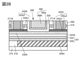
- 2A and 2B are cross-sectional views showing an example of a transistor
- Fig. 3A is a top view illustrating an example of a transistor
- Fig. 3B is a cross-sectional view illustrating an example of a transistor
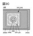
- Figs. 3C and 3D are top views illustrating an example of a transistor
- 4A and 4B are a top view and a cross-sectional view illustrating an example of a transistor
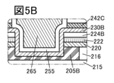
- 5A to 5F are cross-sectional views showing an example of a transistor
- 6A to 6C are cross-sectional views showing an example of a method for manufacturing a semiconductor device.
- FIG. 7A and 7B are cross-sectional views illustrating an example of a method for manufacturing a semiconductor device.
- 8A and 8B are cross-sectional views showing an example of a method for manufacturing a semiconductor device.
- 9A and 9B are cross-sectional views illustrating an example of a method for manufacturing a semiconductor device.
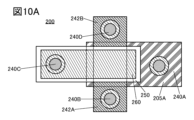
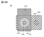
- 10A and 10B are top views illustrating an example of a transistor.
- 11A and 11B are perspective views showing an example of a display device.
- Fig. 12A is a block diagram illustrating an example of the configuration of a display module
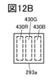
- Fig. 12B is a plan view illustrating an example of the configuration of a pixel circuit
- Fig. 12C and Fig. 12D are circuit diagrams illustrating an example of a configuration including a pixel circuit.
- FIG. 12A is a block diagram illustrating an example of the configuration of a display module
- Fig. 12B is a plan view illustrating an example of the configuration of a pixel circuit
- FIG. 13 is a cross-sectional view showing an example of a display device.
- FIG. 14 is a cross-sectional view showing an example of a display device.
- FIG. 15 is a cross-sectional view showing an example of a display device.
- FIG. 16 is a cross-sectional view showing an example of a display device.
- FIG. 17 is a cross-sectional view showing an example of a display device.
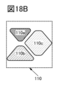
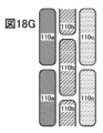
- 18A to 18G are diagrams showing an example of a pixel.
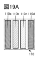
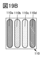
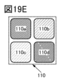
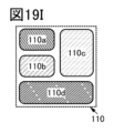
- 19A to 19K are diagrams showing an example of a pixel.
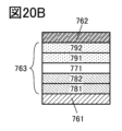
- 20A to 20F are diagrams showing configuration examples of a light-emitting device.
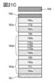
- 21A to 21C are diagrams showing configuration examples of a light-emitting device.
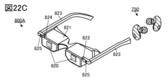
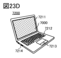
- 22A to 22D are diagrams showing an example of an electronic device.
- 23A to 23F are diagrams showing an example of an electronic device.
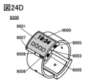
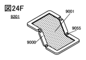
- 24A to 24G are diagrams showing an example of an electronic device.
- ordinal numbers “first” and “second” are used for convenience and do not limit the number of components or the order of the components (e.g., the order of processes or the order of stacking).
- an ordinal number attached to a component in one place in this specification may not match an ordinal number attached to the same component in another place in this specification or in the claims.
- film and “layer” can be interchanged depending on the circumstances.
- conductive layer can be changed to the term “conductive film.”
- insulating film can be changed to the term “insulating layer.”
- a transistor is a type of semiconductor element that can perform functions such as amplifying current or voltage and switching operations that control conduction or non-conduction.
- transistor includes IGFETs (Insulated Gate Field Effect Transistors) and thin film transistors (TFTs).
- source and drain may be interchanged when transistors of different polarity are used, or when the direction of current changes during circuit operation. For this reason, in this specification, the terms “source” and “drain” can be used interchangeably.
- electrically connected includes cases where the connection is made via "something that has some kind of electrical action.”
- something that has some kind of electrical action is not particularly limited as long as it allows the transmission and reception of electrical signals between the connected objects.
- something that has some kind of electrical action includes electrodes or wiring, as well as switching elements such as transistors, resistive elements, coils, and other elements with various functions.
- the off-state current refers to a leakage current between the source and drain when a transistor is in an off state (also referred to as a non-conducting state or a cut-off state).
- the off-state refers to a state in which the voltage Vgs between the gate and source of an n-channel transistor is lower than the threshold voltage Vth (higher than Vth for a p-channel transistor).
- the normally-on characteristic refers to a state in which a channel exists and current flows through the transistor even when no voltage is applied to the gate.
- the normally-off characteristic refers to a state in which no current flows through the transistor when no potential is applied to the gate or when a ground potential is applied to the gate.
- the top surface shape of a certain component refers to the contour shape of the component when viewed from a planar view (also referred to as a top view).
- a planar view refers to a view from the normal direction of the surface on which the component is formed or the surface of the support (e.g., substrate) on which the component is formed.
- top surface shapes roughly match means that at least a portion of the contours of the stacked layers overlap. For example, this includes cases where the upper and lower layers are processed using the same mask pattern, or where a portion of the mask pattern is the same. However, strictly speaking, the contours may not overlap, and the upper layer may be located inside the lower layer, or outside the lower layer, in which case it may also be said that "top surface shapes roughly match.” Furthermore, when the top surface shapes match or roughly match, it can also be said that the edges are aligned or roughly matched, or that the side edges are aligned or roughly matched.
- a tapered shape refers to a shape in which at least a part of the side of the structure is inclined with respect to the substrate surface or the surface to be formed.
- the side of the structure, the substrate surface, and the surface to be formed do not necessarily need to be completely flat, and may be approximately planar with a fine curvature, or approximately planar with fine irregularities.
- an oxynitride refers to a material whose composition contains more oxygen than nitrogen.
- An oxynitride refers to a material whose composition contains more nitrogen than oxygen.
- SIMS secondary ion mass spectrometry
- XPS X-ray photoelectron spectroscopy
- SIMS is suitable when the content of the target element is high (e.g., 0.5 atomic% or more, or 1 atomic% or more).
- SIMS is suitable when the content of the target element is low (e.g., 0.5 atomic% or less, or 1 atomic% or less).
- a device fabricated using a metal mask or an FMM may be referred to as a device with an MM (metal mask) structure.
- a device fabricated without using a metal mask or an FMM may be referred to as a device with an MML (metal maskless) structure.
- SBS Side By Side
- the SBS structure allows the materials and configuration to be optimized for each light-emitting element, which increases the freedom to select materials and configurations and makes it easier to improve brightness and reliability.
- holes or electrons may be referred to as “carriers”.
- the hole injection layer or electron injection layer may be referred to as the "carrier injection layer”
- the hole transport layer or electron transport layer may be referred to as the “carrier transport layer”
- the hole block layer or electron block layer may be referred to as the "carrier block layer”.
- the above-mentioned carrier injection layer, carrier transport layer, and carrier block layer may not be clearly distinguishable.
- one layer may have two or three functions among the carrier injection layer, carrier transport layer, and carrier block layer.
- the light-emitting element has an EL layer between a pair of electrodes.
- the EL layer has at least a light-emitting layer.
- the layers (also called functional layers) that the EL layer has include a light-emitting layer, a carrier injection layer (a hole injection layer and an electron injection layer), a carrier transport layer (a hole transport layer and an electron transport layer), and a carrier block layer (a hole block layer and an electron block layer).
- the light-receiving element also called a light-receiving device
- one of the pair of electrodes may be referred to as a pixel electrode, and the other as a common electrode.
- the sacrificial layer (which may also be referred to as a mask layer) is located at least above the light-emitting layer (more specifically, the layer that is processed into an island shape among the layers that make up the EL layer) and has the function of protecting the light-emitting layer during the manufacturing process.
- step discontinuity refers to the phenomenon in which a layer, film, or electrode is separated due to the shape of the surface on which it is formed (e.g., a step, etc.).
- the semiconductor device of this embodiment has transistors of at least two types of structures on the same plane.
- the transistors of the two types of structures can be formed by sharing some of the processes. For example, by applying one type of transistor to a transistor that requires a large on-current and applying the other type of transistor to a transistor that requires high saturation characteristics, a high-performance semiconductor device can be obtained. More specifically, a vertical transistor with an extremely short channel length is applied to a transistor that requires a large on-current. On the other hand, a planar transistor with a long channel length and a backgate is applied to a transistor that requires high saturation characteristics.
- Fig. 1A shows a top view of a transistor 100
- Fig. 1B shows a top view of a transistor 200
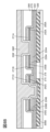
- Fig. 1C shows cross-sectional views of the transistor 100 and the transistor 200.
- Fig. 1C can also be said to be a cross-sectional view in the channel length direction of the transistor 200.
- Fig. 2A shows an enlarged view of the transistor 100
- Fig. 2B shows an enlarged view of the transistor 200.
- Any of the gate, drain, or source of transistor 100 may be electrically connected to any of the gate, drain, or source of transistor 200.
- an insulating layer 275 is provided on the insulating layer 222, on the oxide layer 230B of the transistor 100, and on the oxide layer 230A of the transistor 200, and an insulating layer 280 is provided on the insulating layer 275.
- the insulating layer 275 is located on the oxide layer 230B with the conductive layer 242C and the insulating layer 271C sandwiched therebetween.
- the insulating layer 275 is located on the oxide layer 230A with the conductive layer 242A, the conductive layer 242B, the insulating layer 271A, and the insulating layer 271B sandwiched therebetween.
- the conductive layer 265 of the transistor 100 and the conductive layer 260 of the transistor 200 are provided in the openings of the insulating layer 275 and the insulating layer 280.
- the transistor 100 includes a conductive layer 205B, an oxide layer 230B on the conductive layer 205B, a conductive layer 242C on the oxide layer 230B, an insulating layer 255 on the oxide layer 230B, and a conductive layer 265 on the insulating layer 255.
- the insulating layer 221, the insulating layer 224B, and the insulating layer 271C can also be considered as components of the transistor 100.
- FIG. 1C shows an example in which insulating layer 221 has a laminated structure of insulating layer 220 and insulating layer 222 on insulating layer 220.
- the structure of insulating layer 221 is not limited to this. For example, it may have a structure using only insulating layer 220 or insulating layer 222, or it may have a structure having an additional insulating layer in addition to insulating layer 220 and insulating layer 222.
- Opening 341 is provided so as to penetrate insulating layer 221 and insulating layer 224B
- opening 343 is provided so as to penetrate conductive layer 242
- opening 345 is provided so as to penetrate insulating layer 271C, insulating layer 275, and insulating layer 280.
- opening 343 and opening 345 can be formed, for example, by etching using the same mask.
- opening 343 and opening 345 can be opened, for example, at the same time, so that the sides of the openings may be continuous. Note that, in order to make the figures easier to see, the symbols for opening 341, opening 343, and opening 345 are not shown in Figures 1A and 1C, but are shown in Figure 2A, etc.
- the "side” of an opening can also be expressed as the “sidewall” of the opening.
- Opening 341, opening 343, and opening 345 each overlap with conductive layer 205B. Also, opening 341 and opening 343 have overlapping regions. Also, opening 343 and opening 345 have overlapping regions.
- the oxide layer 230B has a first region that overlaps with the conductive layer 205B on the conductive layer 205B.
- the first region covers the upper surface of the conductive layer 205B.
- the oxide layer 230 is preferably in contact with the upper surface of the conductive layer 205B in the first region.
- the oxide layer 230B also has a second region that covers the side surface of the opening 341 of the insulating layer 221.
- the second region may also cover the side surface of the opening 341 of the insulating layer 224B in addition to the side surface of the opening 341 of the insulating layer 221.
- the oxide layer 230B is located on the insulating layer 221 and the insulating layer 224B and has a third region that overlaps with the conductive layer 242. It is preferable that the conductive layer 242 be in contact with the upper surface of the third region of the oxide layer 230B.
- the first region, the second region, and the third region are preferably a continuous film formed in the same film formation process. Therefore, the first region, the second region, and the third region have, for example, approximately the same film thickness. However, depending on the film formation conditions, the formed film may have a film thickness distribution depending on the region. In the oxide layer 230B, the film thickness in the first region is, for example, 0.7 to 1.3 times the film thickness in the third region.
- the oxide layer 230B, the insulating layer 255, and the conductive layer 265 each have a region that is provided inside the opening 341 of the insulating layer 221.
- the region of the oxide layer 230B that is provided inside the opening 341 may have a portion in common with at least one of the first and third regions described above.
- the oxide layer 230B is provided so as to cover the side surfaces of the insulating layer 221 and the insulating layer 224B.
- the oxide layer 230B, the insulating layer 255, and the conductive layer 265 each have an area that is provided inside the opening 341 of the insulating layer 224B.
- the insulating layer 255 is provided within the opening 341 to cover the oxide layer 230B.
- the insulating layer 255 and the conductive layer 265 each have a region provided inside the opening 343 of the conductive layer 242C, a region provided inside the opening 345 of the insulating layer 271C, a region provided inside the opening 345 of the insulating layer 275, and a region provided inside the opening 345 of the insulating layer 280.
- the conductive layer 265 is provided so as to be embedded inside the opening 345. It is preferable that the insulating layer 255, the conductive layer 265, and the insulating layer 280 have the same or approximately the same height at their upper surfaces.
- the insulating layer 255 functions as a gate insulating layer for the transistor 100.
- the conductive layer 265 functions as a gate electrode for the transistor 100.
- the conductive layer 205B functions as one of the source electrode and drain electrode of the transistor 100.
- the conductive layer 242C functions as the other of the source electrode and drain electrode of the transistor 100.
- the oxide layer 230B has a channel formation region in the transistor 100.
- a region in contact with the conductive layer 205B functions as one of the source region and the drain region
- a region in contact with the conductive layer 242C functions as the other of the source region and the drain region
- a region that functions as a channel formation region is provided between the source region and the drain region.
- At least one of the regions in the oxide layer 230B located between the side surface of the opening 341 in the insulating layer 221 and the conductive layer 265, and the regions located between the side surface of the opening 341 in the insulating layer 224B and the conductive layer 265 functions as a channel formation region of the transistor 100.
- the opening diameter in the insulating layer 221 or the insulating layer 224B corresponds to the channel width of the transistor 100. The diameter of these openings may vary in the depth direction.
- any one of the diameters at the highest position, the diameter at the lowest position, or half the sum of the diameters at the highest position and the lowest position of the insulating layer 221 or the insulating layer 224B in a cross-sectional view may be used.
- the diameter of the opening may be the diameter at the highest point of the insulating layer 220, the diameter at the lowest point of the insulating layer 222, half the sum of the diameters at the highest and lowest points of the insulating layer 220, half the sum of the diameters at the highest and lowest points of the insulating layer 222, etc.
- Figure 2A shows the channel length L100 and channel width W100 of transistor 100.
- channel length L100 can be said to be the shortest distance between the part of oxide layer 230B that contacts conductive layer 242C and the part that contacts conductive layer 205B.
- insulating layer 2223 has a layered structure of insulating layer 220, insulating layer 222, and insulating layer 224B.
- the channel formation region of the oxide layer 230B changes depending on the configuration of the insulating layer 223. For example, depending on the configuration of the insulating layer 223, only a part of the region of the oxide layer 230B that contacts the insulating layer 223 may become the channel formation region, and the channel length L100 may be shorter than the length shown in FIG. 2A.
- an oxide insulating film in the portion of the insulating layer 223 that contacts the channel formation region of the oxide layer 230B.
- an insulating film that releases oxygen when heated e.g., a silicon oxide film, a silicon oxynitride film, etc.
- oxygen vacancies in the channel formation region can be suitably reduced.
- an insulating film through which at least one of oxygen and hydrogen does not easily diffuse can be used on either the top or bottom of the insulating film, or on both sides. It is preferable to use an insulating film through which both oxygen and hydrogen do not easily diffuse.
- a silicon nitride film, a silicon nitride oxide film, an aluminum oxide film, a hafnium oxide film, or the like can be used here. This makes it possible to efficiently supply oxygen to the channel formation region of the oxide layer 230B and to suppress the diffusion of hydrogen into the channel formation region. Therefore, the electrical characteristics of the transistor 100 can be stabilized.
- the insulating layer 224B may have an oxide insulating film, and at least one of the insulating layers 220 and 222 may be an insulating film through which oxygen and hydrogen do not easily diffuse. More specifically, for example, the insulating layer 224B may be a stack of an oxide insulating film and an insulating film through which oxygen and hydrogen do not easily diffuse, in that order from the bottom.
- the insulating layer 222 may be an oxide insulating film
- the insulating layer 220 may be an insulating film through which oxygen and hydrogen are unlikely to diffuse.
- the insulating layer 224B may be configured to have, for example, an insulating film through which oxygen and hydrogen are unlikely to diffuse.
- the channel length L100 of the transistor 100 corresponds to the length of the side of the opening 341 of the insulating layer 223 in a cross-sectional view.
- the channel length L100 is determined by the thickness of the insulating layer 223 and the angle ⁇ 100 between the side of the opening 341 of the insulating layer 223 and the surface on which the insulating layer 223 is to be formed (here, the upper surface of the conductive layer 205B). Therefore, for example, the channel length L100 can be set to a value smaller than the limit resolution of the exposure device, and a transistor of a fine size can be realized.
- a transistor with an extremely small channel length that could not be realized with a conventional exposure device for mass production of flat panel displays (for example, a minimum line width of about 2 ⁇ m or 1.5 ⁇ m).
- a transistor with a channel length of less than 10 nm without using an extremely expensive exposure device used in cutting-edge LSI technology.
- the channel length L100 can be, for example, 5 nm or more, 7 nm or more, or 10 nm or more, and less than 3 ⁇ m, 2.5 ⁇ m or less, 2 ⁇ m or less, 1.5 ⁇ m or less, 1.2 ⁇ m or less, 1 ⁇ m or less, 500 nm or less, 300 nm or less, 200 nm or less, 100 nm or less, 50 nm or less, 30 nm or less, or 20 nm or less.
- the channel length L100 can be 100 nm or more and 1 ⁇ m or less.
- the on-state current of the transistor 100 can be increased.
- the transistor 100 By using the transistor 100, a circuit capable of high-speed operation can be manufactured. Furthermore, the area occupied by the circuit can be reduced. Therefore, a small-sized semiconductor device can be obtained. For example, when the semiconductor device of one embodiment of the present invention is applied to a large display device or a high-definition display device, even if the number of wirings is increased, signal delay in each wiring can be reduced and display unevenness can be suppressed. Furthermore, since the area occupied by the circuit can be reduced, the frame of the display device can be narrowed.
- the channel length L100 can be controlled by adjusting the thickness and angle ⁇ 100 of the insulating layer 223.
- the thickness of the insulating layer 223 can be at least thicker than the oxide layer 230B.
- it can be 2 nm or more, 5 nm or more, 10 nm or more, or 50 nm or more, and 500 nm or less, 400 nm or less, 300 nm or less, 200 nm or less, or 150 nm or less.
- the thickness of the insulating layer 220 can be, for example, 1 nm to 100 nm, 2 nm to 50 nm, 2 nm to 20 nm, or 2 nm to 10 nm.
- the thickness of the insulating layer 222 can be, for example, 2 nm to 200 nm, 3 nm to 100 nm, 5 nm to 50 nm, or 8 nm to 30 nm.
- the thickness of the insulating layer 222 can be, for example, thicker than the insulating layer 220.
- the thickness of the insulating layer 224B can be, for example, 2 nm to 300 nm, 3 nm to 200 nm, 5 nm to 100 nm, or 8 nm to 50 nm.
- the thickness of the insulating layer 224B can be, for example, thicker than the insulating layer 220.
- the side of the opening 341 in the insulating layer 223 is preferably vertical or tapered.
- the angle ⁇ 100 is preferably 90 degrees or less. By reducing the angle ⁇ 100, the coverage of the layer (e.g., oxide layer 230B) provided on the insulating layer 223 can be improved.
- an example is shown in which the side of the opening 341 in the insulating layer 223 is vertical (angle ⁇ 100 is 90 degrees).
- the angle ⁇ 100 can be, for example, 30 degrees or more, 35 degrees or more, 40 degrees or more, 45 degrees or more, 50 degrees or more, 55 degrees or more, 60 degrees or more, 65 degrees or more, or 70 degrees or more, and 90 degrees or less, 85 degrees or less, or 80 degrees or less.
- the angle ⁇ 100 may also be 75 degrees or less, 70 degrees or less, 65 degrees or less, or 60 degrees or less.
- the side of opening 343 in conductive layer 242C is located outside the side of opening 341 in insulating layer 221.
- the side of opening 345 in insulating layer 275 and insulating layer 280 is located outside the side of opening 341 in insulating layer 221.
- FIGS. 3A and 3B show a top view and a cross-sectional view of the transistor 100.
- the transistor 100 shown in FIGS. 3A and 3B has different dimensions from the transistor 100 shown in FIGS. 1A and 1C in order to make it easier to explain the opening 341.
- the top shape of the opening 341 in the insulating layer 221 and the insulating layer 224B, the top shape of the opening 343 in the conductive layer 242C, and the top shape of the opening 345 in the insulating layer 271C, the insulating layer 275, and the insulating layer 280 can each be circular.
- the channel width W100 of the transistor 100 is equal to the circumference of the opening 343. In this way, when the top shape of the opening is circular, a transistor with a smaller channel width can be realized compared to other shapes.
- the top surface shapes of openings 341, 343, and 345 are concentric circles.
- the conductive layer 242C is located outside the opening 341. Therefore, it is preferable that the end of the conductive layer 242C on the opening 343 side is located outside the side end of the insulating layer 221 on the opening 341 side. In addition, it is preferable that the side end of the conductive layer 242C on the opening 343 side is located outside the side end of the insulating layer 224B on the opening 341 side. By making the opening diameter of the opening 343 larger than that of the opening 341, the opening 343 can be located outside the opening 341.
- the end of conductive layer 242C on the opening 343 side may coincide or approximately coincide with the end of opening 341.
- the openings 343 and 345 can be formed using the same mask. Therefore, for example, the opening diameter of the opening 345 is the same or approximately the same as the opening diameter of the opening 343.
- at least one of the side end of the conductive layer 242C on the opening 343 side, the side end of the insulating layer 271C on the opening 345 side, the side end of the insulating layer 275 on the opening 345 side, and the side end of the insulating layer 280 on the opening 345 side is the same or approximately the same. It is preferable that the side end of the insulating layer 275 on the opening 345 side has an area located outside the side end of the insulating layer 221 on the opening 341 side. It is also preferable that the side end of the insulating layer 280 on the opening 345 side has an area located outside the side end of the insulating layer 221 on the opening 341 side.
- the diameter of one opening may be larger than the diameter of the other opening depending on the etching conditions, etc.
- Figures 4A and 4B show a top view and a cross-sectional view of the transistor 100.
- Figures 4A and 4B are modifications of Figures 3A and 3B.
- the centers of the top surface shapes of openings 341 and 343 may be misaligned.
- the top surface shape of opening 341 is circular.
- the top surface shape of opening 343 is also circular, and the opening diameter is larger than that of opening 341.
- the centers of the circles of the top surface shapes of openings 341 and 343 do not coincide.
- opening 341 is located inside opening 343 when viewed from above.
- the oxide layer 230B has a variation in channel length L100, i.e., a variation in the shortest distance between the portion of the oxide layer 230B that contacts the conductive layer 205B and the portion that contacts the conductive layer 242C. Therefore, the configuration shown in Figures 3A and 3B can suppress the variation in channel length compared to the configuration shown in Figures 4A and 4B. On the other hand, the configuration shown in Figures 4A and 4B may be easier to fabricate compared to Figures 3A and 3B.
- the diameter of the opening is equal to or greater than the limit resolution of the exposure device.
- the diameter can be, for example, 20 nm or more, 50 nm or more, 100 nm or more, 200 nm or more, 300 nm or more, 400 nm or more, or 500 nm or more, and less than 5.0 ⁇ m, 4.5 ⁇ m or less, 4.0 ⁇ m or less, 3.5 ⁇ m or less, 3.0 ⁇ m or less, 2.5 ⁇ m or less, 2.0 ⁇ m or less, 1.5 ⁇ m or less, or 1.0 ⁇ m or less.
- the top surface shape of the openings provided in each layer is not limited, and can be, for example, a circle, an ellipse, a triangle, a quadrangle (including a rectangle, a diamond, and a square), a pentagon, a star-shaped polygon, or any other polygon with rounded corners.
- the polygon may be either a concave polygon (a polygon with at least one interior angle exceeding 180 degrees) or a convex polygon (a polygon with all interior angles less than 180 degrees).
- a circle is not limited to a perfect circle.
- the top surface shape of an opening in a film can refer to the shape of the top surface end or the shape of the bottom surface end on the opening side of the film.
- Figures 3C and 3D each show a top view of the transistor 100.
- Figure 3C shows an example in which the top shapes of the openings 341, 343, and 345 are rectangular.
- Figure 3D shows an example in which the top shapes of the openings 341, 343, and 345 are elliptical.
- each island-shaped layer can be, for example, a circle, an ellipse, a triangle, a quadrangle (including a rectangle, a diamond, and a square), a pentagon, a star-shaped polygon, or any other polygon with rounded corners.
- the source electrode and drain electrode are located at different heights, and the current flowing through the oxide layer flows in the height direction.
- the channel length direction has a component in the height direction (vertical direction), so the transistor 100 can also be called a VFET (Vertical Field Effect Transistor), vertical transistor, vertical channel transistor, vertical channel transistor, etc.
- VFET Vertical Field Effect Transistor
- the transistor 100 can have a source electrode, an oxide layer, and a drain electrode stacked on top of each other, the area occupied can be significantly reduced compared to a so-called planar type transistor in which the oxide layer is arranged in a planar shape.
- FIG. 5A shows an enlarged view of the area surrounded by the two-dot chain line in FIG. 1C in the transistor 100. Also, FIG. 5B and FIG. 5C show modified examples of FIG. 5A.
- the conductive layer 205B shown in Figures 5A and 5B has a recess at a position overlapping the opening.
- the conductive layer 205B may not have a recess.
- the oxide layer 230B is provided in contact with the bottom and side surfaces of the recess in the conductive layer 205B. Also, in Figures 5A and 5B, the oxide layer 230B is in contact with the top surface of the conductive layer 205B and has a region located inside the recess in the conductive layer 205B.
- the region of the oxide layer 230B that contacts the side surface of the insulating layer 224B overlaps with the conductive layer 265.
- the region of the oxide layer 230B that contacts the side surface of the insulating layer 224B faces the conductive layer 265.
- the region of the oxide layer 230B that contacts the side surface of the insulating layer 224B functions as a channel formation region of the transistor 100.
- the region of the oxide layer 230B that contacts the side of the insulating layer 224B and the region that contacts the side of the insulating layer 222 overlaps with the conductive layer 265.
- the region of the oxide layer 230B that contacts the side of the insulating layer 224B and the region that contacts the side of the insulating layer 222 face the conductive layer 265. Therefore, compared to the configuration shown in FIG. 5C, the region (offset region) to which the gate electric field is difficult to apply can be reduced, which is preferable. Furthermore, in FIG.
- the region of the oxide layer 230B that contacts the side of the insulating layer 220 also overlaps with the conductive layer 265 (faces the conductive layer 265), so compared to the configuration shown in FIG. 5A, the offset region can be reduced, which is preferable. This makes it possible to suppress the decrease in field effect mobility caused by the offset region.
- the etching selectivity with respect to the conductive layer 205B is high during etching to form an opening in the insulating layer 220, so that the conductive layer 205B is prevented from being broken and reliability can be improved.
- the transistor 200 includes a conductive layer 205A, an insulating layer 221, an insulating layer 224A, an oxide layer 230A, a conductive layer 242A, a conductive layer 242B, an insulating layer 250, and a conductive layer 260. Furthermore, the insulating layer 271A and the insulating layer 271B can also be considered as components of the transistor 200. In addition, in the configuration example shown in FIGS. 1B and 1C, an example is shown in which the insulating layer 221 has a stacked structure of an insulating layer 220 and an insulating layer 222 over the insulating layer 220.
- the insulating layer 250 functions as a gate insulating layer (also referred to as a first gate insulating layer) of the transistor 200.
- the conductive layer 260 functions as a gate electrode (also referred to as a first gate electrode) of the transistor 200.
- the insulating layer 220, the insulating layer 222, and the insulating layer 224A function as a back gate insulating layer (also referred to as a second gate insulating layer) of the transistor 200.
- the conductive layer 205A functions as a back gate electrode (also referred to as a second gate electrode) of the transistor 200.
- the conductive layer 242A functions as one of the source electrode and drain electrode of the transistor 200.
- the conductive layer 242B functions as the other of the source electrode and drain electrode of the transistor 200.
- the oxide layer 230A has a fourth region and a fifth region and a sixth region that are provided so as to sandwich the fourth region.
- the fourth region can function as a channel formation region
- the fifth region can function as one of the source region and the drain region
- the sixth region can function as the other of the source region and the drain region.
- At least a part of the fourth region overlaps with the conductive layer 260.
- One of the fifth region and the sixth region overlaps with the conductive layer 242A, and the other overlaps with the conductive layer 242B.
- At least a part of the first region overlaps with the conductive layer 260 via the insulating layer 250, and overlaps with the conductive layer 205A via the insulating layer 220, the insulating layer 222, and the insulating layer 224A.
- opening 346 is provided so as to penetrate insulating layer 275 and insulating layer 280. To make the figures easier to see, opening 346 is not shown in Figures 1B and 1C, but is shown in Figure 2B etc.
- the insulating layer 250 and the conductive layer 260 have a region provided inside the opening 346 of the insulating layer 275 and a region provided inside the opening 346 of the insulating layer 280.
- Opening 346 overlaps conductive layer 205A.
- the insulating layer 250 is provided to cover the upper surface of the oxide layer 230A, the side of the conductive layer 242A, the side of the conductive layer 242B, the side of the insulating layer 271A, the side of the insulating layer 271B, the side of the opening 346 of the insulating layer 275, and the side of the opening 346 of the insulating layer 280.
- the conductive layer 260 is provided so as to be embedded inside the opening 346. It is preferable that the insulating layer 250, the conductive layer 260, and the insulating layer 280 have the same or approximately the same height at their upper surfaces.
- Figure 5D shows a cross-sectional view of the transistor 200 in the channel width direction.
- Figure 5E shows an enlarged view of the area surrounded by the dashed line in Figure 5D, and a modified example of Figure 5E is shown in Figure 5F.
- the insulating layer 275 and the insulating layer 280 have an opening that reaches the insulating layer 222. Note that there are cases where an opening does not need to be provided in the insulating layer 275. In this case, an opening that reaches the insulating layer 275 is provided in the insulating layer 280.
- a recess may be provided in the insulating layer 222. Alternatively, an opening that reaches the insulating layer 220 may be provided in the insulating layer 222.
- An insulating layer 250 is provided to cover the opening that reaches the oxide layer 230A and the opening that reaches the insulating layer 222 or the insulating layer 220, and a conductive layer 260 is provided on the insulating layer 250.
- a conductive layer 260 is provided on the insulating layer 250.
- the channel length of the transistor 200 can be determined by the width of the conductive layer 260, so there is a higher degree of freedom in designing the channel length compared to the transistor 100, which is a vertical transistor. For example, when a semiconductor device has multiple transistors 200, the channel lengths of all the transistors 200 may be the same, or the channel lengths of some of the transistors 200 may be different from the channel lengths of the other transistors 200. By making the channel length of the transistor 200 longer than the channel length of the transistor 100, the transistor 200 can be made to have good saturation characteristics.
- the channel formation region is a high-resistance region with a low carrier concentration because it has fewer oxygen vacancies or a lower impurity concentration than the source and drain regions. Therefore, the channel formation region can be said to be i-type (intrinsic) or substantially i-type.
- the source and drain regions are low-resistance regions with high carrier concentrations due to a large number of oxygen vacancies or high concentrations of impurities such as hydrogen, nitrogen, and metal elements.
- the source and drain regions are n-type regions (low-resistance regions) with a high carrier concentration compared to the channel formation region.
- the carrier concentration of the channel formation region is preferably 1 ⁇ 10 18 cm ⁇ 3 or less, less than 1 ⁇ 10 17 cm ⁇ 3 , less than 1 ⁇ 10 16 cm ⁇ 3 , less than 1 ⁇ 10 15 cm ⁇ 3 , less than 1 ⁇ 10 14 cm ⁇ 3 , less than 1 ⁇ 10 13 cm ⁇ 3 , less than 1 ⁇ 10 12 cm ⁇ 3 , less than 1 ⁇ 10 11 cm ⁇ 3 , or less than 1 ⁇ 10 10 cm ⁇ 3 .
- the lower limit of the carrier concentration of the channel formation region is not particularly limited, but may be, for example, 1 ⁇ 10 ⁇ 9 cm ⁇ 3 .
- the impurity concentration in the oxide layer 230A and the oxide layer 230B is reduced to reduce the defect state density.
- a low impurity concentration and a low defect state density are referred to as high purity intrinsic or substantially high purity intrinsic.
- An oxide semiconductor (or metal oxide) with a low carrier concentration may be referred to as a high purity intrinsic or substantially high purity intrinsic oxide semiconductor (or metal oxide).
- the impurity concentration in the oxide layer 230B In order to stabilize the electrical characteristics of the transistor 100, it is effective to reduce the impurity concentration in the oxide layer 230B. In order to stabilize the electrical characteristics of the transistor 200, it is effective to reduce the impurity concentration in the oxide layer 230A. In order to reduce the impurity concentrations of the oxide layers 230A and 230B, it is preferable to also reduce the impurity concentration in the adjacent films.
- impurities include hydrogen, nitrogen, alkali metals, alkaline earth metals, iron, nickel, silicon, and the like.
- the impurities in the oxide layer 230A refer to, for example, anything other than the main component constituting the oxide layer 230A. For example, an element with a concentration of less than 0.1 atomic % can be said to be an impurity. The same applies to impurities in the oxide layer 230B.
- the concentrations of metal elements and impurity elements such as hydrogen and nitrogen detected in each region may change continuously within each region, not limited to a gradual change from region to region. In other words, the concentrations of metal elements and impurity elements such as hydrogen and nitrogen may decrease in the region closer to the channel formation region.
- Insulating layer 216, conductive layer 205A, and conductive layer 205B are provided on insulating layer 215. Conductive layer 205A and conductive layer 205B are provided so as to be embedded in the openings of insulating layer 216. It is preferable that insulating layer 216, conductive layer 205A, and conductive layer 205B have the same or approximately the same height at the top surface.
- An insulating layer 221 is provided on the insulating layer 216, the conductive layer 205A, and the conductive layer 205B.
- Insulating layer 224B, oxide layer 230B, conductive layer 242C, and insulating layer 271C are stacked in this order on insulating layer 221 so that at least a portion of them overlap conductive layer 205B.
- the insulating layer 224B, the oxide layer 230B, the conductive layer 242C, and the insulating layer 271C can be processed collectively into an island shape. This can increase the productivity of the semiconductor device.
- the side edge of the conductive layer 242C has an area that coincides or roughly coincides with the side edge of the oxide layer 230B.
- the side edge of the insulating layer 224B has an area that coincides or roughly coincides with the side edge of the oxide layer 230B.
- FIG. 1C When processing the layers into an island shape all at once, for example, a structure as shown in FIG. 1C can be realized. Specifically, in a cross-sectional view of the transistor 100, the side end of the conductive layer 242C coincides or roughly coincides with the side end of the oxide layer 230B. Furthermore, the side end of the insulating layer 224B coincides or roughly coincides with the side end of the oxide layer 230B.
- An insulating layer 271C may be provided on the conductive layer 242C.
- the insulating layer 271C can function as an etching stopper that protects the conductive layer 242C in the process of processing the conductive layer 242C into an island shape at once.
- An insulating layer 275 is provided to cover the side surfaces of insulating layer 224B, oxide layer 230B, conductive layer 242C, and insulating layer 271C, as well as the top surface of insulating layer 271C, and an insulating layer 280 is provided to cover insulating layer 275.
- insulating layer 275 covers the upper surface of conductive layer 242C with insulating layer 271C sandwiched therebetween.
- the insulating layer 255 is provided in contact with the side surface of the conductive layer 242C, the side surface of the insulating layer 271C, the side surface of the insulating layer 275, and the side surface of the insulating layer 280.
- the conductive layer 265 is provided on the insulating layer 255.
- Insulating layer 224A and oxide layer 230A are laminated in this order on insulating layer 221 so that at least a portion of them overlaps conductive layer 205A.
- Conductive layer 242A and conductive layer 242B are provided on oxide layer 230A and spaced apart from each other.
- the insulating layer 224A, the oxide layer 230A, and the conductive layer (conductive layer 242D) that will become the conductive layer 242A and the conductive layer 242B can be processed into an island shape all at once (conductive layer 242D will be described in detail later in FIG. 7A, etc.). This can improve the productivity of the semiconductor device.
- the side edge of the conductive layer 242 has an area that coincides or roughly coincides with the side edge of the oxide layer 230A.
- the side edge of the insulating layer 224A has an area that coincides or roughly coincides with the side edge of the oxide layer 230A.
- one side end of the conductive layer 242A coincides or roughly coincides with one side end of the oxide layer 230A
- one side end of the conductive layer 242B coincides or roughly coincides with the other side end of the oxide layer 230A.
- the side end of the insulating layer 224A coincides or roughly coincides with the side end of the oxide layer 230A.
- An insulating layer 271A may be provided on conductive layer 242A, and an insulating layer 271B may be provided on conductive layer 242B.
- the insulating layer (insulating layer 271D) that becomes insulating layer 271A and insulating layer 271B can function as an etching stopper that protects conductive layer 242D (conductive layer that becomes conductive layer 242A and conductive layer 242B) in the process of processing the conductive layer into an island shape at once (insulating layer 271D will be described in detail later in FIG. 7A, etc.).
- Conductive layer 242A, conductive layer 242B, and conductive layer 242C can be formed by processing the same conductive layer. Also, insulating layer 271A, insulating layer 271B, and insulating layer 271C can be formed by processing the same insulating layer.
- An insulating layer 275 is provided to cover the side surfaces of insulating layer 224A, oxide layer 230A, conductive layer 242A, conductive layer 242B, insulating layer 271A, and insulating layer 271B, as well as the top surfaces of insulating layer 271A and insulating layer 271B, and an insulating layer 280 is provided to cover insulating layer 275.
- insulating layer 275 has a region that covers the upper surface of conductive layer 242A with insulating layer 271A sandwiched therebetween, and a region that covers the upper surface of conductive layer 242B with insulating layer 271B sandwiched therebetween.
- Insulating layer 255 and insulating layer 250 can be formed by processing the same insulating layer.
- the side surfaces of the inner walls of the openings 345 and 346 are preferably vertical or tapered.
- the angle between the side surfaces of the inner walls of the openings 345 and 346 and the surface on which the insulating layer 271 is to be formed is vertical or close to vertical, it is preferable to form the insulating layers that become the insulating layers 255 and 250 using a film formation method with high coverage.
- the structure of a transistor in which the electric field of at least the first gate electrode electrically surrounds the channel formation region is called a surrounded channel (S-channel) structure.
- the S-channel structure disclosed in this specification has a structure different from the Fin type structure and the planar type structure.
- the S-channel structure disclosed in this specification can also be regarded as a type of Fin type structure.
- the Fin type structure refers to a structure in which the gate electrode is arranged to surround at least two or more sides of the channel (specifically, two, three, or four sides, etc.).
- the channel formation region can be electrically surrounded. Since the S-channel structure electrically surrounds the channel formation region, it can be said that it is substantially the same structure as a GAA (Gate All Around) structure or a LGAA (Lateral Gate All Around) structure.
- the transistor 200 By making the transistor 200 have an S-channel structure, a GAA structure, or a LGAA structure, the channel formation region formed at or near the interface between the oxide layer 230A and the insulating layer 250 can be the entire bulk of the oxide layer 230A. Therefore, it is possible to improve the current density flowing through the transistor, and it is expected to improve the on-current of the transistor or the field effect mobility of the transistor.
- insulating layers 282, 283, and 284 are provided on the transistor 100 and the transistor 200.
- an insulating layer 241 is provided on the side of the openings provided in the insulating layers 282, 283, and 284, etc., and it is preferable that the conductive layers 205A to 240G are embedded inside the insulating layer 241.
- Each of conductive layers 240A, 240B, 240C, 240D, 240E, 240F, and 240G can be configured to be electrically connected to other conductive layers via a conductive layer located above insulating layer 284.
- FIGS. 10A and 10B show modified examples of the configurations of transistors 100 and 200 as viewed from the top.
- each layer constituting the semiconductor device of this embodiment, the transistor 100, and the transistor 200 may have a single-layer structure or a stacked-layer structure.
- ⁇ Oxide layer 230A and oxide layer 230B> a metal oxide that functions as a semiconductor (hereinafter also referred to as an oxide semiconductor) is preferably used.
- the oxide layer 230A and the oxide layer 230B have a channel formation region, which is i-type (intrinsic) or substantially i-type.
- the oxide layer 230A and the oxide layer 230B further have a source region and a drain region, which are n-type regions (low resistance regions) with a higher carrier concentration than the channel formation region.
- Oxide layer 230A and oxide layer 230B can be formed in the same process using the same material.
- the crystallinity of the semiconductor material used for the oxide layer 230A and the oxide layer 230B is not particularly limited, and any of an amorphous semiconductor, a single crystal semiconductor, and a semiconductor having crystallinity other than single crystal (a microcrystalline semiconductor, a polycrystalline semiconductor, or a semiconductor having a crystalline region in part) may be used.
- the use of a single crystal semiconductor or a semiconductor having crystallinity is preferable because it can suppress deterioration of the transistor characteristics.
- the band gap of a metal oxide that functions as a semiconductor is preferably 2.0 eV or more, and more preferably 2.5 eV or more.
- a metal oxide with a large band gap By using a metal oxide with a large band gap, the off-current of a transistor can be reduced.
- a transistor having a metal oxide in a channel formation region in this way is called an OS transistor. Since an OS transistor has a small off-current, the power consumption of a semiconductor device can be sufficiently reduced. Furthermore, since an OS transistor has high frequency characteristics, the semiconductor device can operate at high speed.
- metal oxides that can be used for the oxide layer 230A and the oxide layer 230B include indium oxide, gallium oxide, and zinc oxide.
- the metal oxide preferably contains at least indium (In) or zinc (Zn).
- the metal oxide preferably contains two or three elements selected from indium, element M, and zinc.
- the element M is a metal element or semi-metal element that has a high bond energy with oxygen, for example, a metal element or semi-metal element that has a higher bond energy with oxygen than indium.
- element M examples include aluminum, gallium, tin, yttrium, titanium, vanadium, chromium, manganese, iron, cobalt, nickel, zirconium, molybdenum, hafnium, tantalum, tungsten, lanthanum, cerium, neodymium, magnesium, calcium, strontium, barium, boron, silicon, germanium, and antimony.
- the element M of the metal oxide is preferably one or more of the above elements, more preferably one or more selected from aluminum, gallium, tin, and yttrium, and even more preferably gallium.
- metal elements and metalloid elements may be collectively referred to as "metal elements", and the "metal element" described in this specification may include metalloid elements.
- the oxide layer 230A and the oxide layer 230B may be, for example, indium zinc oxide (In-Zn oxide, also referred to as IZO (registered trademark)), indium tin oxide (In-Sn oxide), indium titanium oxide (In-Ti oxide), indium gallium oxide (In-Ga oxide), indium gallium aluminum oxide (In-Ga-Al oxide), indium gallium tin oxide (In-Ga-Sn oxide), gallium zinc oxide (Ga-Zn oxide, also referred to as GZO), aluminum zinc oxide (Al-Zn oxide, also referred to as AZO), indium aluminum Indium zinc oxide (In-Al-Zn oxide, also written as IAZO), indium tin zinc oxide (In-Sn-Zn oxide, also written as ITZO (registered trademark)), indium titanium zinc oxide (In-Ti-Zn oxide), indium gallium zinc oxide (In-Ga-Zn oxide, also written as IGZO), indium gallium
- the field effect mobility of the transistor can be increased.
- a transistor with a large on-current can be realized.
- the metal oxide may contain one or more metal elements having a large periodic number instead of or in addition to indium.
- metal elements having a large periodic number include metal elements belonging to the fifth period and metal elements belonging to the sixth period. Specific examples of the metal elements include yttrium, zirconium, silver, cadmium, tin, antimony, barium, lead, bismuth, lanthanum, cerium, praseodymium, neodymium, promethium, samarium, and europium. Note that lanthanum, cerium, praseodymium, neodymium, promethium, samarium, and europium are called light rare earth elements.
- the metal oxide may also contain one or more nonmetallic elements.
- the carrier concentration may increase or the band gap may be narrowed, which may increase the field effect mobility of the transistor.
- nonmetallic elements include carbon, nitrogen, phosphorus, sulfur, selenium, fluorine, chlorine, bromine, and hydrogen.
- the metal oxide becomes highly crystalline, and the diffusion of impurities in the metal oxide can be suppressed. Therefore, fluctuations in the electrical characteristics of the transistor can be suppressed, and reliability can be improved.
- the formation of oxygen vacancies in the metal oxide can be suppressed. Therefore, carrier generation due to oxygen vacancies can be suppressed, and a transistor with a small off-current can be obtained. Furthermore, fluctuations in the electrical characteristics of the transistor can be suppressed, and reliability can be improved.
- the electrical characteristics and reliability of the transistor vary depending on the composition of the metal oxide applied to the oxide layer 230A and the oxide layer 230B. Therefore, by varying the composition of the metal oxide according to the electrical characteristics and reliability required of the transistor, a semiconductor device that combines excellent electrical characteristics and high reliability can be obtained.
- the metal oxide is an In-M-Zn oxide
- the atomic ratio of In in the In-M-Zn oxide is equal to or greater than the atomic ratio of M.
- the nearby composition includes a range of ⁇ 30% of the desired atomic ratio.
- the atomic ratio of In in the In-M-Zn oxide may be less than the atomic ratio of M.
- the total proportion of the atomic numbers of the metal elements can be regarded as the proportion of the atomic number of element M.
- the ratio of the number of indium atoms to the sum of the numbers of atoms of all metal elements contained may be referred to as the indium content. The same applies to other metal elements.
- the metal oxide can be formed by sputtering or atomic layer deposition (ALD).
- ALD atomic layer deposition
- the composition of the metal oxide after film formation may differ from the composition of the target.
- the zinc content in the metal oxide after film formation may decrease to about 50% compared to the target.
- Oxide layer 230A and oxide layer 230B may have a stacked structure having two or more metal oxide layers.
- the two or more metal oxide layers in oxide layer 230A and oxide layer 230B may have the same or approximately the same composition.
- By having a stacked structure of metal oxide layers with the same composition for example, they can be formed using the same sputtering target, thereby reducing manufacturing costs.
- the two or more metal oxide layers in the oxide layer 230A and the oxide layer 230B may have different compositions.
- gallium, aluminum, or tin as the element M.
- a stacked structure of any one selected from indium oxide, indium gallium oxide, and IGZO and any one selected from IAZO, IAGZO, and ITZO (registered trademark) can be used.
- the oxide layer 230A and the oxide layer 230B preferably have a metal oxide layer having crystallinity.
- a metal oxide having crystallinity examples include a CAAC (c-axis aligned crystal) structure, a polycrystalline structure, and a nano-crystalline (nc: nano-crystal) structure.
- Oxide layer 230A and oxide layer 230B may have a laminated structure of two or more metal oxide layers with different crystallinity.
- a laminated structure of a first metal oxide layer and a second metal oxide layer provided on the first metal oxide layer may be configured so that the second metal oxide layer has a region with higher crystallinity than the first metal oxide layer.
- the second metal oxide layer may have a region with lower crystallinity than the first metal oxide layer.
- the first metal oxide layer and the second metal oxide layer may have different compositions, or may have the same or approximately the same composition.
- the thickness of oxide layer 230A and oxide layer 230B is preferably 1 nm or more and 200 nm or less, more preferably 3 nm or more and 100 nm or less, even more preferably 5 nm or more and 100 nm or less, even more preferably 10 nm or more and 100 nm or less, even more preferably 10 nm or more and 70 nm or less, even more preferably 15 nm or more and 70 nm or less, even more preferably 15 nm or more and 50 nm or less, even more preferably 20 nm or more and 50 nm or less.
- oxide semiconductor When an oxide semiconductor is used for the oxide layer 230A and the oxide layer 230B, hydrogen contained in the oxide semiconductor may react with oxygen bonded to a metal atom to become water, and oxygen vacancies ( VO ) may be formed in the oxide semiconductor. Furthermore, a defect in which hydrogen is introduced into the oxygen vacancy (hereinafter referred to as VOH ) may function as a donor and generate electrons that are carriers. In addition, some of the hydrogen may bond with oxygen bonded to a metal atom to generate electrons that are carriers. Therefore, a transistor using an oxide semiconductor containing a large amount of hydrogen is likely to have normally-on characteristics (that is, a threshold voltage has a negative value). Furthermore, hydrogen in an oxide semiconductor is easily mobile due to stress such as heat or an electric field, and therefore, if an oxide semiconductor contains a large amount of hydrogen, the reliability of the transistor may be deteriorated.
- an oxide semiconductor When an oxide semiconductor is used for the oxide layer 230A and the oxide layer 230B, it is preferable to reduce VOH in the oxide layer 230A and the oxide layer 230B as much as possible to make them highly pure intrinsic or substantially highly pure intrinsic.
- it is important to remove impurities such as water and hydrogen from the oxide semiconductor (sometimes referred to as dehydration or dehydrogenation treatment) and to supply oxygen to the oxide semiconductor to repair oxygen vacancies.
- Stable electrical characteristics can be imparted by using an oxide semiconductor with sufficiently reduced impurities such as VOH for a channel formation region of a transistor. Note that supplying oxygen to an oxide semiconductor to repair oxygen vacancies may be referred to as oxygen addition treatment.
- the carrier concentration of the oxide semiconductor in the region functioning as a channel formation region is preferably 1 ⁇ 10 18 cm ⁇ 3 or less, more preferably less than 1 ⁇ 10 17 cm ⁇ 3 , further preferably less than 1 ⁇ 10 16 cm ⁇ 3 , further preferably less than 1 ⁇ 10 13 cm ⁇ 3 , and further preferably less than 1 ⁇ 10 12 cm ⁇ 3 .
- the lower limit of the carrier concentration of the oxide semiconductor in the region functioning as a channel formation region is not particularly limited, and can be, for example, 1 ⁇ 10 ⁇ 9 cm ⁇ 3 .
- the semiconductor device of this embodiment may also be applied to a transistor using another semiconductor material in the channel formation region.
- another semiconductor material include semiconductors made of single elements, or compound semiconductors.
- semiconductors made of single elements include silicon and germanium.
- compound semiconductors include gallium arsenide and silicon germanium.
- Other examples of compound semiconductors include organic semiconductors and nitride semiconductors.
- the aforementioned oxide semiconductor is also a type of compound semiconductor. Note that these semiconductor materials may contain impurities as dopants.
- Silicon that can be used as a semiconductor material for transistors includes single crystal silicon, polycrystalline silicon, microcrystalline silicon, and amorphous silicon.
- An example of polycrystalline silicon is low temperature polysilicon (LTPS).
- the semiconductor material of the transistor may have a layered material that functions as a semiconductor.
- a layered material is a general term for a group of materials that have a layered crystal structure.
- a layered crystal structure is a structure in which layers formed by covalent or ionic bonds are stacked via bonds weaker than covalent or ionic bonds, such as van der Waals forces.
- a layered material has high electrical conductivity within a unit layer, that is, high two-dimensional electrical conductivity.
- Examples of the layered material include graphene, silicene, and chalcogenides.
- Chalcogenides are compounds containing chalcogen (an element belonging to Group 16).
- Examples of the chalcogenides include transition metal chalcogenides and Group 13 chalcogenides.
- transition metal chalcogenides that can be used as semiconductor materials for transistors include molybdenum sulfide (representatively MoS 2 ), molybdenum selenide (representatively MoSe 2 ), molybdenum tellurium (representatively MoTe 2 ), tungsten sulfide (representatively WS 2 ), tungsten selenide (representatively WSe 2 ), tungsten tellurium (representatively WTe 2 ), hafnium sulfide (representatively HfS 2 ), hafnium selenide (representatively HfSe 2 ), zirconium sulfide (representatively ZrS 2 ), zirconium selenide (representatively ZrSe 2 ), and the like.
- MoS 2 molybdenum sulfide
- MoSe 2 molybdenum selenide
- MoTe 2 moly MoTe 2
- the insulating layer 250 is in contact with a channel formation region of the oxide layer 230A.
- the insulating layer 255 is in contact with a channel formation region of the oxide layer 230B.
- the same materials as those that can be used for the insulating layer 250 can be used.
- the same material as that for the insulating layer 250 may be used, or a different material may be used.
- the insulating layer 250 preferably has a function of capturing and fixing hydrogen, which can reduce the hydrogen concentration in the channel formation region of the oxide layer 230A. As a result, VOH in the channel formation region can be reduced, and the channel formation region can be made i-type or substantially i-type.
- the layer in contact with the oxide layer 230A has the function of capturing and fixing hydrogen.
- the insulating layer 255 has the function of capturing and fixing hydrogen, which can reduce the hydrogen concentration in the channel formation region of the oxide layer 230B.
- the layer in contact with the oxide layer 230B has the function of capturing and fixing hydrogen.
- An example of an insulating layer that has the function of capturing and fixing hydrogen is a metal oxide having an amorphous structure.
- a metal oxide such as magnesium oxide or an oxide containing one or both of aluminum and hafnium.
- oxygen atoms have dangling bonds, and the dangling bonds may have the property of capturing or fixing hydrogen.
- metal oxides having an amorphous structure have a high ability to capture or fix hydrogen.
- a high dielectric constant (high-k) material for the insulating layer 250.
- An example of a high-k material is an oxide containing one or both of aluminum and hafnium.
- an oxide containing one or both of aluminum and hafnium as the layer in contact with the oxide layer 230A in the insulating layer 250, it is more preferable to use an oxide having an amorphous structure and containing one or both of aluminum and hafnium, and it is even more preferable to use aluminum oxide having an amorphous structure.
- aluminum oxide is used as the layer in contact with the oxide layer 230A in the insulating layer 250.
- the layer in contact with the oxide layer 230A in the insulating layer 250 is an insulating layer containing at least oxygen and aluminum.
- the aluminum oxide has an amorphous structure.
- the layer in contact with the oxide layer 230A in the insulating layer 250 has an amorphous structure.
- the insulating layer 250 may have an insulating layer having a thermally stable structure, such as silicon oxide or silicon oxynitride.
- the insulating layer 250 may have an insulating layer with a heat-stable structure between a pair of insulating layers that have the function of capturing and fixing hydrogen.
- Insulating layer 250 preferably has a barrier insulating layer against oxygen. This can suppress oxidation of conductive layer 242A, conductive layer 242B, conductive layer 260, etc.
- insulating layer 250 has a laminated structure, it is preferable that the layer in contact with conductive layer 242A and conductive layer 242B, and the layer in contact with conductive layer 260 are each a barrier insulating layer against oxygen.
- the insulating layer 255 has a barrier insulating layer against oxygen, oxidation of the conductive layer 242C and the conductive layer 265 can be suppressed.
- the layer in contact with the conductive layer 242C and the layer in contact with the conductive layer 265 are each a barrier insulating layer against oxygen.
- a barrier insulating layer refers to an insulating layer that has barrier properties.
- barrier properties refer to a function of suppressing the diffusion of the corresponding substance (also called low permeability), or a function of capturing and fixing the corresponding substance (also called gettering).
- Examples of the barrier insulating layer against oxygen include oxides containing one or both of aluminum and hafnium, magnesium oxide, gallium oxide, indium gallium zinc oxide, silicon nitride, and silicon nitride oxide.
- Examples of oxides containing one or both of aluminum and hafnium include aluminum oxide, hafnium oxide, oxides containing aluminum and hafnium (hafnium aluminate), and oxides containing hafnium and silicon (hafnium silicate).
- the barrier insulating layer against oxygen is preferably less permeable to oxygen than at least the insulating layer 280.
- the layer in the insulating layer 250 that is in contact with the conductive layer 242A and the conductive layer 242B is preferably less permeable to oxygen than at least the insulating layer 280.
- the layer has a barrier property against oxygen, which can prevent the side surfaces of the conductive layer 242A and the conductive layer 242B from being oxidized and an oxide film from being formed on the side surfaces. This can prevent a decrease in the on-current of the transistor 200 or a decrease in the field effect mobility.
- the insulating layer 250 is provided in contact with the upper surface of the insulating layer 222, the side of the insulating layer 224A, and the upper surface and side of the oxide layer 230A.
- the insulating layer 250 has a barrier property against oxygen, so that the layer in contact with these can suppress the desorption of oxygen from the channel formation region of the oxide layer 230A when heat treatment is performed. Therefore, the formation of oxygen vacancies in the oxide layer 230A can be suppressed. Even if the insulating layer 280 contains an excessive amount of oxygen, the oxygen can be suppressed from being excessively supplied to the oxide layer 230A, and an appropriate amount of oxygen can be supplied to the oxide layer 230A through the insulating layer 250. Therefore, the source region and drain region of the oxide layer 230A are excessively oxidized, and the decrease in the on-current of the transistor 200 and the decrease in the field effect mobility can be suppressed.
- the thickness of the insulating layer 250 is preferably 0.1 nm or more and 30 nm or less, preferably 0.1 nm or more and 20 nm or less, preferably 0.1 nm or more and 10 nm or less, more preferably 0.1 nm or more and 5.0 nm or less, more preferably 0.5 nm or more and 5.0 nm or less, more preferably 1.0 nm or more and less than 5.0 nm, and even more preferably 1.0 nm or more and 3.0 nm or less.
- the ALD method includes the thermal ALD method, in which the reaction between the precursor and the reactant is carried out using only thermal energy, and the plasma enhanced ALD (PEALD) method, in which a plasma excited reactant is used.
- the PEALD method may be preferable because it uses plasma, which allows film formation at a lower temperature.
- the ALD method can deposit atoms one layer at a time, which has the advantages of enabling extremely thin films to be formed, films to be formed on structures with high aspect ratios, films with fewer defects such as pinholes, films with excellent coverage, and films to be formed at low temperatures. Therefore, the insulating layer 250 can be formed with good coverage on the side surfaces of the openings formed in the insulating layer 280, etc., and on the side ends of the conductive layers 242A and 242B, etc., with a thin film thickness as described above.
- films formed by the ALD method may contain more impurities such as carbon than films formed by other film formation methods.
- Quantitative determination of impurities can be performed using secondary ion mass spectrometry (SIMS), X-ray photoelectron spectroscopy (XPS), or Auger electron spectroscopy (AES).
- the insulating layer 275 is preferably a barrier insulating layer against oxygen because it can suppress oxidation of the conductive layers 242A, 242B, 242C, etc.
- the insulating layer 241 is preferably a barrier insulating layer against oxygen because it can suppress oxidation of the conductive layers 240A to 240G.
- insulating layer 250 For information about the barrier insulating layer against oxygen, please refer to the description of insulating layer 250.
- the insulating layer 275 is a barrier insulating layer against hydrogen, it is preferable because it can suppress a decrease in the hydrogen concentration in the source and drain regions of the oxide layer 230A.
- Barrier insulating layers against hydrogen include oxides such as aluminum oxide, hafnium oxide, and tantalum oxide, and nitrides such as silicon nitride.
- the insulating layers 215 and 221 are provided under the transistors 100 and 200.
- the insulating layers 282 and 282 are provided to cover the upper sides of the transistors 100 and 200.
- the insulating layer 221 has a laminated structure of the insulating layer 220 and the insulating layer 222 on the insulating layer 220.
- the structure of the insulating layer 221 is not limited to this.
- the insulating layer 221 may have a structure using only the insulating layer 220 or the insulating layer 222, or may have a further insulating layer in addition to the insulating layer 220 and the insulating layer 222.
- the insulating layer described in this specification can be used as appropriate as the insulating layer.
- an insulating layer that has a function of suppressing the diffusion of impurities such as hydrogen and water is an insulating layer that covers one or both of the top and bottom of the transistors 100 and 200. Therefore, it is preferable that at least one of the insulating layers located on the bottom side of the transistors 100 and 200 is an insulating layer that has a function of suppressing the diffusion of hydrogen. In addition, it is preferable that at least one of the insulating layers that covers the top side of the transistors 100 and 200 is an insulating layer that has a function of suppressing the diffusion of hydrogen.
- an insulating layer that releases oxygen As an insulating layer in contact with the oxide layer 230B and the oxide layer 230A.
- oxygen can be efficiently supplied to the oxide layer.
- At least one of the insulating layers 215, 220, 222, 282, and 283 preferably functions as a barrier insulating layer that suppresses diffusion of impurities such as water and hydrogen from the substrate side or from above the transistor to the transistor 100. Therefore, at least one of the insulating layers 215, 220, 222, 282, and 283 preferably has an insulating material that has a function of suppressing diffusion of impurities such as hydrogen atoms, hydrogen molecules, water molecules, nitrogen atoms, nitrogen molecules, nitrogen oxide molecules (N 2 O, NO, NO 2 , etc.), and copper atoms (through which the above impurities are difficult to permeate). Alternatively, it is preferable to have an insulating material that has a function of suppressing diffusion of oxygen (for example, at least one of oxygen atoms and oxygen molecules, etc.) (through which the above oxygen is difficult to permeate).
- oxygen for example, at least one of oxygen atoms and oxygen molecules, etc.
- an insulating layer having a function of suppressing the diffusion of impurities such as water and hydrogen, and oxygen for example, aluminum oxide, magnesium oxide, hafnium oxide, zirconium oxide, oxide containing aluminum and hafnium (hafnium aluminate), oxide containing hafnium and zirconium (hafnium zirconium oxide), gallium oxide, or silicon nitride oxide can be used.
- silicon nitride which has a higher hydrogen barrier property, as the insulating layer 283 and the insulating layer 220.
- the insulating layer 282 has aluminum oxide or magnesium oxide, which has a high function of capturing and fixing hydrogen, respectively.
- hafnium oxide which is a high dielectric constant (high-k) material, which has a high ability to capture or fix hydrogen, as the insulating layer 222.
- the insulating layer 224A and the insulating layer 224B can be formed in the same process and from the same material.
- the insulating layer 224A is preferably an oxide since it is in contact with the oxide layer 230A.
- the insulating layer 224B is preferably an oxide since it is in contact with the oxide layer 230B.
- the insulating layer 224A and the insulating layer 224B preferably have silicon oxide or silicon oxynitride. This allows oxygen to be supplied from the insulating layer 224A to the oxide layer 230A, thereby reducing oxygen vacancies. Similarly, oxygen can be supplied from the insulating layer 224B to the oxide layer 230B, thereby reducing oxygen vacancies.
- the insulating layer 224A is preferably processed into an island shape, similar to the oxide layer 230A. As a result, when multiple transistors 200 are provided, an insulating layer 224A of approximately the same size is provided for each transistor 200. As a result, the amount of oxygen supplied from the insulating layer 224A to the oxide layer 230A in each transistor 200 becomes approximately the same. Therefore, it is possible to suppress the variation in the electrical characteristics of the transistors 200 within the substrate surface. However, this is not limited to the above, and similar to the insulating layer 220, the insulating layer 224 may be configured not to be patterned.
- Each of the insulating layers 216, 280, and 284 preferably has a dielectric constant lower than that of the insulating layer 222.
- each of the insulating layers 216, 280, and 284 preferably has a dielectric constant lower than that of the insulating layer 220.
- insulating layer 216, insulating layer 280, and insulating layer 284 each have one or more of silicon oxide, silicon oxynitride, silicon oxide doped with fluorine, silicon oxide doped with carbon, silicon oxide doped with carbon and nitrogen, and silicon oxide having vacancies.
- silicon oxide and silicon oxynitride are preferred because they are thermally stable.
- materials such as silicon oxide, silicon oxynitride, and silicon oxide with vacancies are preferred because they can easily form regions containing oxygen that is released by heating.
- insulating layer 216, insulating layer 280, and insulating layer 284 may each be planarized.
- the concentration of impurities such as water and hydrogen in the insulating layer 280 is reduced.
- the insulating layer 280 has an oxide containing silicon, such as silicon oxide or silicon oxynitride.
- the conductive layer 205A, the conductive layer 205B, and the conductive layers 242A to 242C may each have a single-layer structure or a stacked-layer structure.
- the conductive layer 205A and the conductive layer 205B can be formed in the same process using the same material.
- the conductive layers 242A to 242C can be formed in the same process using the same material.
- Materials that can be used for the conductive layers 205A, 205B, and 242A to 242C include, for example, one or more of chromium, copper, aluminum, gold, silver, zinc, tantalum, titanium, tungsten, manganese, nickel, iron, cobalt, molybdenum, and niobium, and alloys containing one or more of the above-mentioned metals.
- Low-resistance conductive materials containing one or more of copper, silver, gold, and aluminum can be preferably used for the conductive layers 205A, 205B, and 242A to 242C. Copper or aluminum is particularly preferred because of its excellent mass productivity.
- the conductive layer 205B and the conductive layers 242A to 242C are conductive layers in contact with the oxide layer, and therefore it is preferable to use a conductive material that is not easily oxidized, a conductive material that maintains low electrical resistance even when oxidized, an oxide conductive material, or a conductive material that has a function of suppressing oxygen diffusion.
- the conductive material include a conductive material containing nitrogen and a conductive material containing oxygen. This can suppress a decrease in the conductivity of the conductive layer 205B and the conductive layers 242A to 242C.
- the conductive layer 205A, the conductive layer 205B, and the conductive layers 242A to 242C can each be made of an oxide conductor.
- oxide conductors include indium oxide, zinc oxide, In-Sn oxide (ITO), In-Zn oxide, In-W oxide, In-W-Zn oxide, In-Ti oxide, In-Ti-Sn oxide, In-Sn-Si oxide (also referred to as ITO containing silicon, ITSO), zinc oxide to which gallium is added, and In-Ga-Zn oxide.
- ITO In-Sn oxide
- ITO In-Zn oxide
- In-W oxide In-W-Zn oxide
- In-Ti oxide In-Ti-Sn oxide
- ITSO In-Sn-Si oxide
- conductive oxides containing indium are preferable because of their high conductivity.
- a metal oxide that has become a conductor can be called an oxide conductor.
- the conductive layer 205A, the conductive layer 205B, and the conductive layers 242A to 242C may each have a stacked structure of a conductive film containing the above-mentioned oxide conductor (metal oxide) and a conductive film containing a metal or an alloy.
- a conductive film containing a metal or an alloy By using a conductive film containing a metal or an alloy, the wiring resistance can be reduced.
- the conductive layer 205A, the conductive layer 205B, and the conductive layers 242A to 242C may each be a Cu-X alloy film (X is Mn, Ni, Cr, Fe, Co, Mo, Ta, or Ti).
- X is Mn, Ni, Cr, Fe, Co, Mo, Ta, or Ti.
- the conductive layer 205A, the conductive layer 205B, and the conductive layers 242A to 242C are preferably made of, for example, titanium, tantalum nitride, titanium nitride, a nitride containing titanium and aluminum, a nitride containing tantalum and aluminum, ruthenium, ruthenium oxide, ruthenium nitride, an oxide containing strontium and ruthenium, or an oxide containing lanthanum and nickel. These are preferable because they are conductive materials that are difficult to oxidize or materials that maintain their conductivity even when oxidized.
- the conductive layer 205B and the conductive layers 242A to 242C have a stacked structure, it is preferable to use a conductive material that is difficult to oxidize at least for the layer in contact with the oxide layer 230A or the oxide layer 230B.
- the conductive layer 205A, the conductive layer 205B, and the conductive layers 242A to 242C may each include a nitride conductor.
- nitride conductors include tantalum nitride and titanium nitride.
- the conductive layer 205A, the conductive layer 205B, and the conductive layers 242A to 242C can each have a single-layer structure of an oxide conductor film, a stacked structure of a metal film and an oxide conductor film, or a stacked structure of a metal film.
- An example of an oxide conductor film is an ITSO film.
- An example of a metal film is a single-layer structure of a tungsten film, a single-layer structure of a titanium film, a single-layer structure of a copper film, and a three-layer structure of a titanium film, an aluminum film, and a titanium film.
- an ITSO film for the conductive layer 205A, the conductive layer 205B, and the conductive layers 242A to 242C.
- the conductive layer 242A and the conductive layer 242B are each shown as a two-layer structure.
- the conductive layer 242A is a laminated film of the conductive layer 242a1 and the conductive layer 242a2 on the conductive layer 242a1
- the conductive layer 242B is a laminated film of the conductive layer 242b1 and the conductive layer 242b2 on the conductive layer 242b1.
- a metal nitride for example, a nitride containing tantalum, a nitride containing titanium, a nitride containing molybdenum, a nitride containing tungsten, a nitride containing tantalum and aluminum, or a nitride containing titanium and aluminum.
- a nitride containing tantalum is particularly preferable.
- ruthenium, ruthenium oxide, ruthenium nitride, an oxide containing strontium and ruthenium, an oxide containing lanthanum and nickel, or the like may be used. These materials are preferable because they are conductive materials that are difficult to oxidize or materials that maintain their conductivity even when they absorb oxygen.
- tantalum nitride or titanium nitride can be used for the conductive layer 242a1 and the conductive layer 242b1, and tungsten can be used for the conductive layer 242a2 and the conductive layer 242b2.
- the conductive layer 260 and the conductive layer 265 may each have a single-layer structure or a laminated structure.
- materials that can be used for the conductive layer 260 and the conductive layer 265 include one or more of chromium, copper, aluminum, gold, silver, zinc, tantalum, titanium, tungsten, manganese, nickel, iron, cobalt, molybdenum, and niobium, and alloys containing one or more of the above-mentioned metals.
- a low-resistance conductive material containing one or more of copper, silver, gold, and aluminum can be suitably used. In particular, copper or aluminum is preferable because of its excellent mass productivity.
- An oxide conductor can be used for the conductive layer 260 and the conductive layer 265.
- Examples of the oxide conductor include the materials exemplified in the description of the conductive layer 205A, etc.
- the conductive layer 260 and the conductive layer 265 may have a stacked structure of a conductive film containing the oxide conductor (metal oxide) described above and a conductive film containing a metal or an alloy. By using a conductive film containing a metal or an alloy, the wiring resistance can be reduced.
- Conductive layer 260 and conductive layer 265 may be made of a Cu-X alloy film (X is Mn, Ni, Cr, Fe, Co, Mo, Ta, or Ti). By using a Cu-X alloy film, the film can be processed by a wet etching process, which reduces manufacturing costs.
- X is Mn, Ni, Cr, Fe, Co, Mo, Ta, or Ti.
- a three-layer stacked structure of a titanium film, an aluminum film, and a titanium film for the conductive layer 260 and the conductive layer 265.
- FIG. 2B shows an example in which the conductive layer 260 has a two-layer structure.
- the conductive layer 260 shown in FIG. 2B has a conductive layer 260a and a conductive layer 260b arranged on the conductive layer 260a.
- the conductive layer 260a is preferably arranged so as to surround the bottom and side surfaces of the conductive layer 260b.
- the conductive layer 260a is preferably made of a conductive material having a function of suppressing the diffusion of impurities such as hydrogen atoms, hydrogen molecules, water molecules, nitrogen atoms, nitrogen molecules ( N2O , NO, NO2 , etc.), nitrogen oxide molecules, copper atoms, etc.
- impurities such as hydrogen atoms, hydrogen molecules, water molecules, nitrogen atoms, nitrogen molecules ( N2O , NO, NO2 , etc.), nitrogen oxide molecules, copper atoms, etc.
- it is preferably made of a conductive material having a function of suppressing the diffusion of oxygen (for example, at least one of oxygen atoms and oxygen molecules, etc.).
- the conductive layer 260a has a function of suppressing the diffusion of oxygen, which can suppress the conductive layer 260b from being oxidized by oxygen contained in the insulating layer 280, etc., and thereby suppressing a decrease in conductivity.
- a conductive material having a function of suppressing the diffusion of oxygen it is preferable to use, for example, titanium, titanium nitride, tantalum, tantalum nitride, ruthenium, ruthenium oxide, etc.
- the conductive layer 260b is preferably a conductive layer having high conductivity.
- the conductive layer 260b may be made of a conductive material containing tungsten, copper, or aluminum as a main component.
- the conductive layer 260b may also have a layered structure, for example, a layered structure of titanium or titanium nitride and the above-mentioned conductive material.
- conductive layer 260 and conductive layer 265 are each formed in a self-aligned manner so as to fill an opening formed in insulating layer 280 or the like. By forming them in this manner, conductive layer 260 can be positioned so as to overlap the region between conductive layer 242A and conductive layer 242B without alignment. Similarly, conductive layer 265 can also be positioned at a predetermined position without alignment.
- Each of the conductive layer 240A, the conductive layer 240B, the conductive layer 240C, the conductive layer 240D, the conductive layer 240E, the conductive layer 240F, and the conductive layer 240G may have a single layer structure or a laminated structure.
- a conductive material having a function of suppressing the permeation of impurities such as water and hydrogen is preferably used as the layer in contact with the insulating layer 241.
- a single layer structure or a stacked structure using one or more of tantalum, tantalum nitride, titanium, titanium nitride, ruthenium, and ruthenium oxide can be used. This can suppress impurities such as water and hydrogen from being mixed into the oxide layer 230A, etc. through the conductive layers 240A to 240G.
- the conductive layers 240A to 240G also function as wirings, it is preferable that the conductive layers have high conductivity.
- a conductive material containing tungsten, copper, or aluminum as a main component can be used.
- Conductive layers 240A to 240G preferably have a two-layer structure of, for example, titanium nitride and tungsten.
- the insulating layers 271A, 271B, and 271C are inorganic insulating layers that function as an etching stopper when the conductive layers 242A, 242B, and 242C are processed, and protect the conductive layers 242A, 242B, and 242C.
- the insulating layers 271A, 271B, and 271C are in contact with the conductive layers 242A, 242B, and 242C, they are preferably inorganic insulating layers that are unlikely to oxidize the conductive layers 242A, 242B, and 242C.
- the insulating layer 271A, the insulating layer 271B, and the insulating layer 271C preferably have a two-layer structure, and a nitride insulating film (such as silicon nitride or silicon nitride oxide) is preferably used as a layer in contact with the conductive layer 242A, the conductive layer 242B, and the conductive layer 242C, and an oxide insulating film is preferably formed on the nitride insulating film as an etching stopper.
- a nitride insulating film such as silicon nitride or silicon nitride oxide
- an oxide insulating film is preferably formed on the nitride insulating film as an etching stopper.
- the oxide insulating film for example, an oxide insulating film that can be used for the insulating layer 250 can be used, and specifically, silicon oxide can be mentioned.
- the semiconductor device of this embodiment has transistors of at least two types of structures formed on the same plane using some common processes.
- transistors that require a large on-current vertical transistors with an extremely short channel length are used.
- planar transistors with a long channel length and a backgate are used. This makes it possible to realize a high-performance semiconductor device.
- the thin films (insulating films, semiconductor films, conductive films, etc.) that make up semiconductor devices can be formed using sputtering, chemical vapor deposition (CVD), vacuum deposition, pulsed laser deposition (PLD), ALD, etc.
- Sputtering methods include RF sputtering, which uses a high-frequency power supply as the sputtering power source, DC sputtering, which uses a direct current power supply, and pulsed DC sputtering, which changes the voltage applied to the electrodes in a pulsed manner.
- RF sputtering is mainly used when depositing insulating films
- DC sputtering is mainly used when depositing metal conductive films.
- Pulsed DC sputtering is mainly used when depositing compounds such as oxides, nitrides, and carbides using reactive sputtering.
- CVD methods can also be classified into plasma CVD (PECVD) methods, which use plasma, thermal CVD (TCVD: Thermal CVD) methods, which use heat, and photo CVD (Photo CVD) methods, which use light. They can also be further classified into metal CVD (MCVD: Metal CVD) methods and metal organic CVD (MOCVD: Metal CVD) methods, depending on the source gas used.
- PECVD plasma CVD
- TCVD Thermal CVD
- Photo CVD Photo CVD
- MCVD Metal CVD
- MOCVD Metal CVD
- the plasma CVD method can produce high-quality films at relatively low temperatures.
- the thermal CVD method is a film formation method that can reduce plasma damage to the workpiece because it does not use plasma.
- wiring, electrodes, elements (transistors, capacitive elements, etc.) included in a semiconductor device may become charged up by receiving electric charge from the plasma. At this time, the accumulated electric charge may destroy the wiring, electrodes, elements, etc. included in the semiconductor device.
- thermal CVD method which does not use plasma, such plasma damage does not occur, so the yield of semiconductor devices can be increased.
- plasma damage does not occur during film formation, so a film with fewer defects can be obtained.
- the ALD method can be a thermal ALD method in which the reaction between the precursor and reactant is carried out using only thermal energy, or a PEALD method in which a plasma-excited reactant is used.
- the CVD and ALD methods are different from sputtering methods in which particles emitted from a target or the like are deposited. Therefore, they are film formation methods that are less affected by the shape of the workpiece and have good step coverage.
- the ALD method has excellent step coverage and excellent thickness uniformity, making it suitable for coating the surfaces of openings with high aspect ratios.
- the ALD method since the ALD method has a relatively slow film formation speed, it may be preferable to use it in combination with other film formation methods such as the CVD method, which has a fast film formation speed.
- the CVD method can form a film of any composition by adjusting the flow rate ratio of the source gases.
- the CVD method can form a film whose composition changes continuously by changing the flow rate ratio of the source gases while forming the film.
- the time required for film formation can be shortened compared to forming a film using multiple film formation chambers because no time is required for transportation or pressure adjustment. Therefore, the productivity of semiconductor devices can be increased in some cases.
- a film of any composition can be formed by simultaneously introducing multiple different types of precursors.
- a film of any composition can be formed by controlling the number of cycles of each precursor.
- the thin films (insulating films, semiconductor films, conductive films, etc.) constituting the semiconductor device can be formed by wet film formation methods such as spin coating, dip coating, spray coating, inkjet printing, dispensing, screen printing, offset printing, doctor knife method, slit coating, roll coating, curtain coating, or knife coating.
- the thin film when processing the thin film that constitutes the semiconductor device, a photolithography method or the like can be used.
- the thin film may be processed by a nanoimprint method, a sandblasting method, a lift-off method, or the like.
- an island-shaped thin film may be directly formed by a film formation method using a shielding mask such as a metal mask.
- the light used for exposure can be, for example, i-line (wavelength 365 nm), g-line (wavelength 436 nm), h-line (wavelength 405 nm), or a mixture of these.
- ultraviolet light, KrF laser light, ArF laser light, etc. can also be used.
- Exposure can also be performed by immersion exposure technology.
- Extreme ultraviolet (EUV) light or X-rays can also be used as the light used for exposure.
- Electron beams can also be used instead of the light used for exposure. Extreme ultraviolet light, X-rays, or electron beams are preferable because they enable extremely fine processing. When exposure is performed by scanning a beam such as an electron beam, a photomask is not required.
- Dry etching, wet etching, sandblasting, etc. can be used to etch thin films.
- an insulating layer 216 is formed on an insulating layer 215, and an opening is formed in the insulating layer 216 so as to reach the insulating layer 215.
- conductive layers that become conductive layers 205A and 205B are formed on the insulating layer 215 and the insulating layer 216.
- CMP chemical mechanical polishing
- the insulating layer 215 and the insulating layer 216 can be formed by a sputtering method, a CVD method, an MBE method, a PLD method, or an ALD method.
- a sputtering method it is not necessary to use molecules containing hydrogen in the deposition gas, and therefore the hydrogen concentration in the insulating layer can be reduced, which is preferable.
- the insulating layers 215 and 216 are deposited in succession without exposing them to the atmosphere.
- a multi-chamber deposition apparatus This can reduce the amount of hydrogen in the insulating layers 215 and 216, and can also reduce the incorporation of hydrogen into the films between each deposition process.
- a recess may be formed in insulating layer 215.
- the conductive layers that become conductive layer 205A and conductive layer 205B can be formed using a sputtering method, a CVD method, an MBE method, a PLD method, an ALD method, a plating method, or the like.
- a portion of the insulating layer 216 may be removed.
- insulating layers 220, 222, and 224 are formed on conductive layer 205A, conductive layer 205B, and insulating layer 216 ( Figure 6A).
- the insulating layer 220, the insulating layer 222, and the insulating layer 224 are processed using a lithography method to provide an opening 341 in the portion of the insulating layer 220, the insulating layer 222, and the insulating layer 224 that overlaps with the conductive layer 205B (FIG. 6B).
- the opening 341 By providing the opening 341, the upper surface of the conductive layer 205B is exposed.
- insulating layer 220, insulating layer 222, and insulating layer 224 are opened at the same time.
- the above processing can be performed using a dry etching method or a wet etching method.
- the dry etching method is preferred because it is suitable for fine processing.
- insulating layer 220, insulating layer 222, and insulating layer 224 may be performed under different conditions.
- the exposed conductive layer 205B is preferably etched.
- This etching preferably provides a recess in the area of conductive layer 205B that overlaps with opening 341.
- the depth of the recess is preferably shallower than the film thickness of conductive layer 205B. In other words, this etching preferably does not provide an opening penetrating conductive layer 205B, and conductive layer 205B preferably remains at the bottom of the recess.
- This type of etching in which the conductive layer 205B film remains in the etched area, is sometimes called half etching.
- the resist is exposed through a mask.
- the exposed area is then removed or left using a developer to form a resist mask.
- a conductive layer, a semiconductor, or an insulating layer can be processed into a desired shape by etching through the resist mask.
- a resist mask can be formed by exposing the resist using KrF excimer laser light, ArF excimer laser light, EUV (Extreme Ultraviolet) light, or the like.
- a liquid immersion technique may be used in which a liquid (e.g., water) is filled between the substrate and the projection lens and exposure is performed.
- an electron beam or an ion beam may be used instead of the light described above.
- a mask may not be used.
- the resist mask that is no longer needed after processing can be removed by performing a dry etching process such as ashing using oxygen plasma (hereinafter sometimes referred to as oxygen plasma treatment), a wet etching process, a dry etching process followed by a wet etching process, or a wet etching process followed by a dry etching process.
- a dry etching process such as ashing using oxygen plasma (hereinafter sometimes referred to as oxygen plasma treatment), a wet etching process, a dry etching process followed by a wet etching process, or a wet etching process followed by a dry etching process.
- a hard mask made of an insulating layer or a conductive layer may be used under the resist mask. Etching of the insulating layer 224 etc. may be performed after removing the resist mask, or may be performed while leaving the resist mask. In the latter case, the resist mask may disappear during etching. After etching of the insulating layer 220, the hard mask may be removed by etching. On the other hand, if the material of the hard mask does not affect the subsequent process or can be used in the subsequent process, it is not necessarily necessary to remove the hard mask.
- a configuration may be adopted in which an SOC (Spin On Carbon) film and an SOG (Spin On Glass) film are formed between the workpiece and the resist mask.
- SOC Spin On Carbon
- SOG Spin On Glass
- a SOC film, an SOG film, and a resist mask can be formed in this order on the workpiece, and then lithography can be performed.
- an etching gas containing halogen can be used, specifically, an etching gas containing one or more of fluorine, chlorine, and bromine can be used.
- an etching gas containing one or more of fluorine, chlorine, and bromine can be used.
- C4F6 gas , C5F6 gas , C4F8 gas, CF4 gas, SF6 gas, CHF3 gas, CH2F2 gas, Cl2 gas, BCl3 gas, SiCl4 gas, or BBr3 gas can be used alone or in a mixture of two or more gases.
- oxygen gas, carbon dioxide gas, nitrogen gas, helium gas, argon gas, hydrogen gas, or hydrocarbon gas can be appropriately added to the above etching gas.
- a gas containing no halogen gas but a hydrocarbon gas or hydrogen gas can be used as the etching gas.
- the hydrocarbon used in the etching gas may be one or more of methane ( CH4 ), ethane ( C2H6 ) , propane ( C3H8 ), butane ( C4H10 ), ethylene (C2H4), propylene (C3H6), acetylene (C2H2), and propyne (C3H4 ) .
- the etching conditions may be appropriately set according to the object to be etched.
- a capacitively coupled plasma (CCP) etching device having parallel plate electrodes can be used as the dry etching device.
- the capacitively coupled plasma etching device having parallel plate electrodes may be configured to apply a high frequency voltage to one of the parallel plate electrodes. Or, it may be configured to apply a plurality of different high frequency voltages to one of the parallel plate electrodes. Or, it may be configured to apply a high frequency voltage of the same frequency to each of the parallel plate electrodes. Or, it may be configured to apply a high frequency voltage of different frequencies to each of the parallel plate electrodes.
- a dry etching device having a high density plasma source can be used.
- an inductively coupled plasma (ICP) etching device can be used as the dry etching device having a high density plasma source.
- ICP inductively coupled plasma
- an oxide layer 230 is formed to cover the upper and side surfaces of the insulating layer 224, the side surfaces of the insulating layer 222, the side surfaces of the insulating layer 220, and the upper surface of the exposed conductive layer 205B, and a conductive layer 242 and an insulating layer 271 are formed in this order on the oxide layer 230 ( Figure 6C).
- an insulating film into which one or more of oxygen, hydrogen, and water do not easily diffuse can be used as the insulating layer 220 and the insulating layer 222.
- an insulating film that releases oxygen when heated as one or more of the insulating layer 222 and the insulating layer 224 can be used as the insulating layer 220 and the insulating layer 222.
- insulating layer 224 is a film having a large etching selectivity with respect to insulating layer 222.
- silicon oxide or silicon oxynitride may be used as insulating layer 224, and aluminum oxide, hafnium oxide, an oxide containing aluminum and hafnium (hafnium aluminate), an oxide containing hafnium and silicon (hafnium silicate), or hafnium zirconium oxide may be used as insulating layer 222.
- silicon nitride or silicon nitride oxide may be used as insulating layer 220.
- the insulating layer 220, the insulating layer 222, and the insulating layer 224 can each be formed using, for example, a sputtering method, a CVD method, an MBE method, a PLD method, or an ALD method.
- the insulating layer 224 is preferably formed by a sputtering method. This eliminates the need to use hydrogen-containing molecules in the deposition gas, and therefore the hydrogen concentration in the insulating layer 224 can be reduced. Since the oxide layer 230 is provided on and in contact with the insulating layer 224, it is preferable that the hydrogen concentration in the insulating layer 224 is reduced.
- heat treatment may be performed before the formation of the insulating layer 224.
- the heat treatment may be performed under reduced pressure, and the insulating layer 224 may be formed continuously without exposure to the air.
- moisture and hydrogen adsorbed on the surface of the insulating layer 222 can be removed, and the moisture concentration and hydrogen concentration in the insulating layer 222 can be further reduced.
- the temperature of the heat treatment is preferably 100° C. or higher and 400° C. or lower. In this embodiment, the temperature of the heat treatment is 250° C.
- the oxide layer 230 can be formed, for example, using a sputtering method, a CVD method, an MBE method, a PLD method, or an ALD method.
- the oxide layer 230 is formed by a sputtering method
- oxygen or a mixed gas of oxygen and a noble gas is used as the sputtering gas.
- the amount of excess oxygen in the oxide film to be formed can be increased.
- an In-M-Zn oxide target or the like can be used.
- the proportion of oxygen contained in the sputtering gas is preferably 70% or more, more preferably 80% or more, and even more preferably 100%.
- an oxygen-excessive oxide semiconductor is formed when the ratio of oxygen contained in the sputtering gas is set to more than 30% and not more than 100%, preferably 70% to 100%.
- a transistor using an oxygen-excessive oxide semiconductor in a channel formation region can have relatively high reliability.
- one embodiment of the present invention is not limited thereto.
- An oxygen-deficient oxide semiconductor is formed when the ratio of oxygen contained in the sputtering gas is set to 1% to 30%, preferably 5% to 20%, when the oxide layer 230 is formed.
- a transistor using an oxygen-deficient oxide semiconductor in a channel formation region can have relatively high field-effect mobility.
- the crystallinity of the oxide layer can be improved by forming the oxide layer while heating the substrate.
- the oxide layer 230 it is preferable to form the oxide layer 230 using the ALD method.
- the oxide layer By forming the oxide layer using the ALD method, a thin film can be formed with good controllability.
- the insulating layer 224 and the oxide layer 230 without exposing them to the atmosphere.
- the heat treatment may be performed within a temperature range in which the oxide layer 230 does not become polycrystallized.
- the temperature of the heat treatment is preferably 100°C or higher, 250°C or higher, or 350°C or higher, and 650°C or lower, 600°C or lower, or 550°C or lower.
- the heat treatment is performed in an atmosphere of nitrogen gas or an inert gas, or an atmosphere containing 10 ppm or more, 1% or more, or 10% or more of an oxidizing gas.
- an atmosphere of nitrogen gas or an inert gas or an atmosphere containing 10 ppm or more, 1% or more, or 10% or more of an oxidizing gas.
- the heat treatment may be performed under reduced pressure.
- the heat treatment may be performed in an atmosphere containing 10 ppm or more, 1% or more, or 10% or more of an oxidizing gas to compensate for the oxygen that has been released.
- the gas used in the heat treatment is preferably highly purified.
- the amount of moisture contained in the gas used in the heat treatment is preferably 1 ppb or less, more preferably 0.1 ppb or less, and even more preferably 0.05 ppb or less.
- the heat treatment is performed at a temperature of 450° C. for 1 hour with a flow rate ratio of nitrogen gas and oxygen gas of 4:1.
- This heat treatment including oxygen gas can reduce impurities such as carbon, water, and hydrogen in the oxide layer 230.
- impurities such as carbon, water, and hydrogen in the oxide layer 230.
- the crystallinity of the oxide layer 230 can be improved, and a denser and more compact structure can be obtained.
- This increases the crystalline region in the oxide layer 230, and reduces the in-plane variation of the crystalline region in the oxide layer 230. Therefore, the in-plane variation of the electrical characteristics of the transistor can be reduced.
- the insulating layer 224 has a portion that functions as a gate insulating layer of the transistor 200
- the oxide layer 230 has a portion that functions as a channel formation region of the transistor 200.
- the transistor 200 formed using the insulating layer 224 and the oxide layer 230 in which the hydrogen concentration is reduced has good reliability and is therefore preferable.
- the conductive layer 242 is formed on the oxide layer 230 without an etching process or the like, so that the upper surface of the oxide layer 230 can be protected by the conductive layer 242. This makes it possible to suppress the diffusion of impurities into the oxide layer 230 that constitutes the transistor, and improve the electrical characteristics and reliability of the semiconductor device.
- the conductive layer 242 can be formed using a sputtering method, a CVD method, an MBE method, a PLD method, a plating method or an ALD method.
- heat treatment may be performed before the conductive layer 242 is formed.
- the heat treatment may be performed under reduced pressure, and the conductive layer 242 may be formed continuously without exposure to the air. By performing such treatment, moisture and hydrogen adsorbed on the surface of the oxide layer 230A can be removed, and the moisture concentration and hydrogen concentration in the oxide layer 230A can be further reduced.
- the temperature of the heat treatment is preferably 100° C. or higher and 400° C. or lower. In this embodiment, the temperature of the heat treatment is set to 250° C.
- the insulating layer 271 can be formed using a method such as sputtering, CVD, MBE, PLD, or ALD.
- heat treatment may be performed before the insulating layer 271 is formed.
- the heat treatment may be performed under reduced pressure, and the insulating layer 271 may be formed continuously without exposure to the air. By performing such treatment, moisture and hydrogen adsorbed on the surface of the conductive layer 242 can be removed, and the moisture concentration and hydrogen concentration in the conductive layer 242 can be further reduced.
- the temperature of the heat treatment is preferably 100° C. or higher and 400° C. or lower. In this embodiment, the temperature of the heat treatment is set to 250° C.
- the insulating layer 224, the oxide layer 230, the conductive layer 242, and the insulating layer 271 are processed into an island shape using lithography to form insulating layer 224A, insulating layer 224B, oxide layer 230A, oxide layer 230B, conductive layer 242C, conductive layer 242D, insulating layer 271C, and insulating layer 271D ( Figure 7A). Note that in areas where these are not provided, the insulating layer 222 is exposed.
- a laminated structure of insulating layer 224A, oxide layer 230A, conductive layer 242D, and insulating layer 271D is formed so that at least a portion of the insulating layer 224A overlaps with conductive layer 205A.
- a laminated structure of insulating layer 224B, oxide layer 230B, conductive layer 242C, and insulating layer 271C is formed so that at least a portion of the insulating layer 224B overlaps with conductive layer 205B.
- the side end of the insulating layer 271D approximately coincides with the side end of the conductive layer 242D. Furthermore, it is preferable that the side end of the conductive layer 242D approximately coincides with the side end of the oxide layer 230A. Furthermore, it is preferable that the side end of the insulating layer 224A approximately coincides with the side end of the oxide layer 230A. Similarly, it is preferable that the side end of the insulating layer 271C approximately coincides with the side end of the conductive layer 242C.
- the side end of the conductive layer 242C approximately coincides with the side end of the oxide layer 230B. Furthermore, it is preferable that the side end of the insulating layer 224B approximately coincides with the side end of the oxide layer 230B.
- an insulating layer 275 can be provided in contact with the side of the insulating layer 224A, the side of the insulating layer 224B, and the top surface of the insulating layer 222 in a process described below.
- the insulating layer 224A and the insulating layer 224B can be separated from the insulating layer 280 by the insulating layer 275.
- the above processing can be performed using a dry etching method or a wet etching method.
- the dry etching method is preferred because it is suitable for fine processing.
- the insulating layers 271C and 271D formed by processing the insulating layer 271 can function as an etching stopper to protect the conductive layers 242C and 242D when the conductive layer 242, the oxide layer 230, and the insulating layer 224 are processed together.
- the insulating layer 271, the conductive layer 242, the oxide layer 230, and the insulating layer 224 may be processed under different conditions.
- a hard mask made of an insulating layer or a conductive layer may be used under a resist mask formed by lithography.
- a hard mask an insulating layer or a conductive layer that will be the hard mask material is formed on the insulating layer 271, a resist mask is formed thereon, and the hard mask material is etched to form a hard mask of a desired shape.
- Etching of the insulating layer 271 etc. may be performed after removing the resist mask, or may be performed while leaving the resist mask. In the latter case, the resist mask may disappear during etching.
- the hard mask may be removed by etching after etching of the oxide layer 230 etc.
- insulating layer 271 can be processed to form insulating layer 271C and insulating layer 271D, and insulating layer 271C and insulating layer 271D can be used as a hard mask in processing conductive layer 242, oxide layer 230, etc.
- the hard mask can be processed so that the layer below the hard mask has roughly the same top surface shape as the hard mask itself.
- the conductive layer 242C and the conductive layer 242D can function as a hard mask in processing the oxide layer 230. That is, the oxide layer 230B and the oxide layer 230A can be formed by processing the oxide layer 230 using the conductive layer 242C and the conductive layer 242D as a hard mask.
- insulating layer 275 is formed on insulating layer 222 so as to cover the laminated structure of insulating layer 224A, oxide layer 230A, conductive layer 242D, and insulating layer 271D, and the laminated structure of insulating layer 224B, oxide layer 230B, conductive layer 242C, and insulating layer 271C, and further, insulating layer 280 is formed on insulating layer 275 ( Figure 7B).
- the insulating layer 280 it is preferable to form an insulating layer that will become the insulating layer 280 and then perform a CMP process on the insulating layer to form an insulating film with a flat upper surface.
- the insulating layer 275 and the insulating layer 280 can each be formed using, for example, a sputtering method, a CVD method, an MBE method, a PLD method, or an ALD method.
- a silicon nitride film as the insulating layer 275 by using the PEALD method.
- the laminated structure of oxide layer 230A and conductive layer 242D and the laminated structure of oxide layer 230B and conductive layer 242C can be covered with insulating layer 275, which has the function of suppressing the diffusion of oxygen.
- the insulating layer 280 by forming silicon oxide using a sputtering method.
- the insulating layer By forming the insulating layer to be the insulating layer 280 by a sputtering method in an atmosphere containing oxygen, the insulating layer 280 containing excess oxygen can be formed.
- the hydrogen concentration in the insulating layer 280 can be reduced.
- a heat treatment may be performed before the formation of the insulating film. The heat treatment may be performed under reduced pressure, and the insulating film may be continuously formed without exposure to the atmosphere.
- moisture and hydrogen adsorbed on the surface of the insulating layer 275 and the like can be removed, and the moisture concentration and hydrogen concentration in the oxide layer 230A, the insulating layer 224A, the oxide layer 230B, and the insulating layer 224B can be further reduced.
- the heat treatment conditions described above can be used for the heat treatment.
- the conductive layer 242D, the insulating layer 271D, the conductive layer 242C, the insulating layer 271C, the insulating layer 275, and the insulating layer 280 are processed by lithography to form the conductive layer 242A, the conductive layer 242B, the insulating layer 271A, the insulating layer 271B, the conductive layer 242C having the opening 343, the insulating layer 271C having the opening 345, and the insulating layer 275 and the insulating layer 280 having the openings 345 and 346 (FIG. 8A).
- the openings 343 and 345 are provided so as to overlap the area where the conductive layer 205B and the oxide layer 230B overlap.
- the opening 346 is provided so as to overlap the area where the oxide layer 230A and the conductive layer 205A overlap.
- a dry etching method or a wet etching method can be used for the above processing.
- a dry etching method is preferable because it is suitable for fine processing.
- a dry etching method is suitable for forming an opening with a high aspect ratio because it is possible to perform anisotropic etching. Note that the above description can be referred to for the conditions of the dry etching method and the dry etching apparatus.
- the insulating layer 271C and the insulating layer 271D can be processed simultaneously.
- the conductive layer 242C and the conductive layer 242D can be processed simultaneously.
- the insulating layer 280, the insulating layer 275, the insulating layer 271D, and the conductive layer 242D can be processed under different conditions.
- the conductive layer 242D is divided into island-shaped conductive layers 242A and 242B.
- the insulating layer 271D is divided into island-shaped insulating layers 271A and 271B.
- the width of the opening is preferably fine because it is reflected in the channel length of the transistor 200.
- the width of the opening is preferably 60 nm or less, 50 nm or less, 40 nm or less, 30 nm or less, 20 nm or less, or 10 nm or less, and 1 nm or more, or 5 nm or more.
- a lithography method can be performed by depositing an SOC film, an SOG film, and a resist mask in that order on the insulating layer 280.
- a resist mask with an opening is formed using short-wavelength light such as EUV light or an electron beam, and the SOG film, the SOC film, the insulating layer 280, the insulating layer 275, the insulating layer 271C and the insulating layer 271D, the conductive layer 242C and the conductive layer 242D are processed using the resist mask.
- the etching process may cause impurities to adhere to the top surface of the oxide layer 230A, the top surface of the oxide layer 230B, the side surfaces of the conductive layers 242A and 242B, the side surfaces of the conductive layer 242C, the side surfaces of the insulating layers 271A and 271B, the side surfaces of the insulating layer 271, the side surfaces of the insulating layer 275, and the side surfaces of the insulating layer 280, or the diffusion of the impurities into these.
- a process for removing such impurities may be performed.
- the dry etching may cause damaged areas to be formed on the surfaces of the oxide layer 230A and the oxide layer 230B. Such damaged areas may be removed.
- Examples of the impurities include components contained in the insulating layer 280, the insulating layer 275, the insulating layer 271C, the insulating layer 271D, the conductive layer 242C, and the conductive layer 242D, components contained in the members of the device used to form the opening, and components contained in the gas or liquid used for etching.
- Examples of the impurities include hafnium, aluminum, silicon, tantalum, fluorine, and chlorine.
- impurities such as aluminum and silicon may reduce the crystallinity of the oxide layer 230A and the oxide layer 230B. Therefore, it is preferable that impurities such as aluminum and silicon are removed from the surface and its vicinity in the oxide layer 230A and the oxide layer 230B. It is also preferable that the concentration of the impurities is reduced.
- the concentration of aluminum atoms in the surface and its vicinity is preferably 5.0 atomic % or less, more preferably 2.0 atomic % or less, more preferably 1.5 atomic % or less, even more preferably 1.0 atomic % or less, and even more preferably less than 0.3 atomic %.
- impurities such as aluminum and silicon reduce the density of the crystal structure in low-crystallinity regions in the oxide layers 230A and 230B, which causes a large amount of VOH to be formed and makes the transistors more likely to be normally on. Therefore, it is preferable that the low-crystallinity regions in the oxide layers 230A and 230B be reduced or removed.
- oxide layer 230A and oxide layer 230B have a layered CAAC structure.
- the oxide layer 230A has a CAAC structure up to the bottom end of the drain.
- the conductive layer 242A or the conductive layer 242B functions as the drain.
- the oxide layer 230A near the bottom end of the conductive layer 242A or the conductive layer 242B has a CAAC structure. In this way, even at the drain end, which significantly affects the drain breakdown voltage, the low-crystalline region of the oxide layer 230A is removed, and by having the CAAC structure, the fluctuation in the electrical characteristics of the transistor 200 can be further suppressed. In addition, the reliability of the transistor 200 can be improved.
- a cleaning process is performed to remove impurities that have adhered to the surface of the oxide layer during the etching process.
- Cleaning methods include wet cleaning using a cleaning solution (also known as wet etching), plasma treatment using plasma, and cleaning by heat treatment, and the above cleaning methods may be combined as appropriate. Note that the cleaning process may deepen the grooves.
- wet cleaning may be performed using an aqueous solution of one or more of ammonia water, oxalic acid, phosphoric acid, and hydrofluoric acid diluted with carbonated water or pure water, pure water, carbonated water, etc.
- ultrasonic cleaning may be performed using these aqueous solutions, pure water, or carbonated water.
- these cleaning methods may be combined as appropriate.
- an aqueous solution in which hydrofluoric acid is diluted with pure water may be referred to as diluted hydrofluoric acid
- an aqueous solution in which ammonia water is diluted with pure water may be referred to as diluted ammonia water.
- the concentration and temperature of the aqueous solution are adjusted as appropriate depending on the impurities to be removed and the configuration of the semiconductor device to be cleaned.
- the ammonia concentration of the diluted ammonia water is preferably 0.01% or more and 5% or less, and more preferably 0.1% or more and 0.5% or less.
- the hydrogen fluoride concentration of the diluted hydrofluoric acid is preferably 0.01 ppm or more and 100 ppm or less, and more preferably 0.1 ppm or more and 10 ppm or less.
- a frequency of 200 kHz or more it is preferable to use a frequency of 200 kHz or more, and more preferably a frequency of 900 kHz or more. By using such a frequency, damage to the oxide layer, etc. can be reduced.
- the above cleaning process may be performed multiple times, and the cleaning solution may be changed for each cleaning process.
- a first cleaning process may be performed using diluted hydrofluoric acid or diluted ammonia water
- a second cleaning process may be performed using pure water or carbonated water.
- wet cleaning is performed using diluted ammonia water.
- impurities attached to the surface of the oxide layer or diffused inside the oxide layer can be removed.
- crystallinity of the oxide layer can be improved.
- Heat treatment may be performed after the etching or cleaning.
- the temperature of the heat treatment is preferably 100° C. or more, 250° C. or more, or 350° C. or more, and 650° C. or less, 600° C. or less, 550° C. or less, or 400° C. or less.
- the heat treatment is performed in an atmosphere of nitrogen gas or inert gas, or an atmosphere containing 10 ppm or more, 1% or more, or 10% or more of an oxidizing gas.
- the crystallinity of the oxide layer 230A can be improved.
- the supplied oxygen reacts with hydrogen remaining in the oxide layer, and the hydrogen can be removed as H 2 O (dehydrated). This prevents hydrogen remaining in the oxide layer from recombining with oxygen vacancies to form VOH .
- the heat treatment may be performed under reduced pressure. Alternatively, after heat treatment in an oxygen atmosphere, heat treatment may be successively performed in a nitrogen atmosphere without exposure to the air.
- the sheet resistance may decrease in the region of the oxide layer 230A that overlaps with the conductive layer 242A and the region that overlaps with the conductive layer 242B.
- the carrier concentration may also increase.
- the sheet resistance may decrease and the carrier concentration may increase in the region of the oxide layer 230B that overlaps with the conductive layer 242C. Therefore, the resistance of the region of the oxide layer that overlaps with the conductive layer can be reduced in a self-aligned manner.
- an insulating layer 250f is formed so as to fill the opening, and a conductive layer 260f is formed on the insulating layer 250f (FIG. 8B).
- the insulating layer 250f and the conductive layer 260f are polished by CMP until the insulating layer 280 is exposed.
- the portions of the insulating layer 250f and the conductive layer 260f exposed from the opening are removed.
- the insulating layer 255 and the conductive layer 265 are formed in the openings 343 and 345, and the insulating layer 250 and the conductive layer 260 are formed in the openings 346.
- the insulating layer 255 is provided in the opening 341 so as to cover the oxide layer 230.
- the insulating layer 255 is preferably provided in contact with the inner walls of the opening 343 and the inner walls of the opening 345.
- the conductive layer 265 is arranged so as to fill the opening 341 via the oxide layer 230 and the insulating layer 255, and is arranged so as to fill the openings 343 and 345 via the insulating layer 255. In this manner, the transistor 100 is formed.
- the insulating layer 250 is preferably provided in contact with the upper surface of the oxide layer 230A, the side of the conductive layer 242A, the side of the conductive layer 242B, the side of the insulating layer 271A, the side of the insulating layer 271B, and the inner wall of the opening 346.
- the conductive layer 260 is arranged to cover the side of the conductive layer 242A, the side of the conductive layer 242B, the side of the insulating layer 271A, and the side of the insulating layer 271B through the insulating layer 250, and is arranged to fill the opening 346 through the insulating layer 250. In this manner, the transistor 200 is formed.
- the insulating layer 250f can be formed, for example, by a sputtering method, a CVD method, an MBE method, a PLD method, or an ALD method. It is preferable to form the insulating layer by the ALD method. It is preferable to form the insulating layer 250 and the insulating layer 255 with a thin film thickness, and it is necessary to reduce the variation in the film thickness.
- the ALD method is a film formation method in which a precursor and a reactant (e.g., an oxidizing agent, etc.) are alternately introduced, and the film thickness can be adjusted by the number of times this cycle is repeated, so that precise film thickness adjustment is possible.
- the insulating layer 250 and the insulating layer 255 need to be formed with good coverage on the bottom and side surfaces of the opening.
- layers of atoms can be deposited one by one on the bottom and side surfaces of the opening, so that the insulating layer 250 and the insulating layer 255 can be formed with good coverage on the opening.
- ozone ( O3 ), oxygen ( O2 ), water ( H2O ), etc. can be used as an oxidizing agent.
- Ozone ( O3 ), oxygen ( O2 ), etc. that do not contain hydrogen it is possible to reduce hydrogen that diffuses into the oxide layer 230A and hydrogen that diffuses into the oxide layer 230B.
- the insulating layer 250f can be formed, for example, by depositing aluminum oxide by thermal ALD, silicon oxide by PEALD, and silicon nitride by PEALD to form a three-layer insulating film.
- a four-layer insulating film can be formed by depositing hafnium oxide between silicon oxide and silicon nitride by thermal ALD.
- the microwave treatment refers to a treatment using a device having a power source that generates high-density plasma using microwaves, for example.
- microwave refers to electromagnetic waves having a frequency of 300 MHz or more and 300 GHz or less.
- the microwave treatment is not necessarily performed after all layers are formed.
- a microwave treatment may be performed after forming aluminum oxide and silicon oxide, and then a silicon nitride film may be formed.
- a microwave treatment may be performed after forming aluminum oxide and silicon oxide, and then a hafnium oxide film may be formed, and then a microwave treatment may be performed, and then a silicon nitride film may be formed.
- the microwave treatment in an atmosphere containing oxygen may be performed multiple times (at least two times or more).
- the microwave treatment it is preferable to use a microwave treatment device having a power source that generates high-density plasma using microwaves.
- the frequency of the microwave treatment device is preferably 300 MHz or more and 300 GHz or less, more preferably 2.4 GHz or more and 2.5 GHz or less, and can be, for example, 2.45 GHz.
- the power of the power source that applies microwaves of the microwave treatment device is preferably 1000 W or more and 10000 W or less, and preferably 2000 W or more and 5000 W or less.
- the microwave treatment device may have a power source that applies RF to the substrate side.
- oxygen ions generated by high-density plasma can be efficiently guided into the oxide layer 230A and the oxide layer 230B.
- the microwave treatment is preferably carried out under reduced pressure, with the pressure being preferably 10 Pa to 1000 Pa, and more preferably 300 Pa to 700 Pa.
- the treatment temperature is preferably 750° C. or less, and more preferably 500° C. or less, and can be, for example, about 250° C.
- a heat treatment may be carried out continuously without exposure to the outside air.
- the temperature of the heat treatment is, for example, preferably 100° C. to 750° C., and more preferably 300° C. to 500° C.
- the microwave treatment can be performed using oxygen gas and argon gas.
- the oxygen flow ratio (O 2 /(O 2 +Ar)) is greater than 0% and less than 100%.
- the oxygen flow ratio (O 2 /(O 2 +Ar)) is greater than 0% and less than 50%. More preferably, the oxygen flow ratio (O 2 /(O 2 +Ar)) is greater than 10% and less than 40%. More preferably, the oxygen flow ratio (O 2 /(O 2 +Ar)) is greater than 10% and less than 30%.
- oxygen gas By performing microwave treatment in an atmosphere containing oxygen, oxygen gas can be turned into plasma using microwaves or high frequency such as RF, and the oxygen plasma can be applied to the channel formation region of the oxide layer 230A, the channel formation region of the oxide layer 230B, and the like.
- VOH in the region By the action of plasma, microwaves, or the like, VOH in the region can be divided into oxygen vacancies and hydrogen, and hydrogen can be removed from the region.
- an insulating film e.g., aluminum oxide having a function of capturing and fixing hydrogen as a layer on the side in contact with the oxide layer 230A and the oxide layer 230B.
- the oxygen injected into the channel formation region can take various forms, such as oxygen atoms, oxygen molecules, oxygen ions, and oxygen radicals (also called O radicals, which are atoms, molecules, or ions with an unpaired electron).
- the oxygen injected into the channel formation region may take one or more of the above forms, and is particularly preferably an oxygen radical.
- the film quality of the insulating layer 250 and the insulating layer 255 can be improved, thereby improving the reliability of the transistor.
- the conductive layer 242A and the conductive layer 242B can function as a shielding film against the action of microwaves, high frequency waves such as RF, oxygen plasma, and the like.
- the conductive layer 242A and the conductive layer 242B can be configured to have a function of shielding electromagnetic waves of 300 MHz or more and 300 GHz or less, for example, 2.4 GHz or more and 2.5 GHz or less.
- the conductive layers 242A and 242B are configured to block the action of microwaves, high frequency waves such as RF, oxygen plasma, and the like, a reduction in VOH and an excessive supply of oxygen can be suppressed in the source and drain regions of the transistor 200, and a decrease in the carrier concentration can be prevented.
- an insulating layer 250 having a barrier property against oxygen in contact with the side surfaces of the conductive layers 242A, 242B, and 242C and an insulating layer 255 having a barrier property against oxygen in contact with the side surface of the conductive layer 242C, it is possible to prevent an oxide film from being formed on the side surfaces of the conductive layers 242A, 242B, and 242C by microwave processing.
- the film quality of insulating layer 250 and insulating layer 255 can be improved, thereby improving the reliability of the transistor.
- thermal energy may be transferred and heating may occur due to electromagnetic interaction between the microwaves and the molecules in the oxide layer 230A or the oxide layer 230B.
- This type of heating process may be called microwave annealing.
- microwave annealing By performing microwave processing in an atmosphere containing oxygen, an effect equivalent to that of oxygen annealing may be obtained. It is also considered that the thermal energy is transferred to hydrogen in the oxide layer 230A or the oxide layer 230B, which activates the hydrogen and causes it to be released from the oxide layer 230A.
- microwave processing may be performed before forming the insulating film, rather than after forming the insulating layer 250f.
- a heat treatment may be performed while maintaining the reduced pressure state.
- hydrogen in the insulating film, the oxide layer 230A, and the oxide layer 230B can be efficiently removed.
- some of the hydrogen may be gettered to the conductive layer 242A, the conductive layer 242B, or the conductive layer 242C.
- the step of performing the heat treatment may be repeated multiple times while maintaining the reduced pressure state.
- the heat treatment temperature is preferably 300°C or higher and 500°C or lower.
- the microwave treatment i.e., microwave annealing, may also serve as the heat treatment. If the oxide layer 230A, etc., is sufficiently heated by the microwave annealing, the heat treatment may not be performed.
- the diffusion of hydrogen, water, impurities, etc. can be suppressed. Therefore, by performing post-processing such as film formation of the insulating layer 250f or post-treatment such as heat treatment, it is possible to suppress the diffusion of hydrogen, water, impurities, etc. through the insulating layer 250f into the oxide layer 230A.
- the conductive layer 260f can be formed, for example, by sputtering, CVD, MBE, PLD, plating, or ALD.
- a titanium nitride film is formed as the conductive layer 260f by ALD, and then a tungsten film is formed by CVD, forming a two-layer conductive film.
- insulating layer 282 is formed on insulating layer 255, conductive layer 265, insulating layer 250, conductive layer 260, and insulating layer 280, insulating layer 283 is formed on insulating layer 282, and insulating layer 284 is formed on insulating layer 283 ( Figure 9A).
- the insulating layer 282, the insulating layer 283, and the insulating layer 284 can each be formed by, for example, a sputtering method, a CVD method, an MBE method, a PLD method, or an ALD method.
- the insulating layer 282, the insulating layer 283, and the insulating layer 284 are each preferably formed by a sputtering method.
- a sputtering method that does not require the use of molecules containing hydrogen in the film formation gas, the hydrogen concentration in the insulating layer 282, the insulating layer 283, and the insulating layer 284 can be reduced.
- insulating layer 282 is formed by forming aluminum oxide by pulse DC sputtering using an aluminum target in an atmosphere containing oxygen gas
- insulating layer 283 is formed by forming silicon nitride by sputtering
- insulating layer 284 is formed by forming silicon oxide by sputtering.
- oxygen can be added to the insulating layer 280 while the layer is being deposited. This allows the insulating layer 280 to contain excess oxygen. At this time, it is preferable to deposit the insulating layer 282 while heating the substrate.
- heat treatment may be performed before the formation of the insulating layer 282.
- the heat treatment may be performed under reduced pressure, and the insulating layer 282 may be formed continuously without exposure to the air. By performing such treatment, moisture and hydrogen adsorbed on the surface of the insulating layer 280 can be removed, and the moisture concentration and hydrogen concentration in the insulating layer 280 can be further reduced.
- the temperature of the heat treatment is preferably 100° C. or higher and 400° C. or lower. In this embodiment, the temperature of the heat treatment is set to 250° C.
- the insulating layer 282 and the insulating layer 283 in succession without exposing them to the air environment.
- openings are formed in insulating layers 220, 275, 280, 282, 283, and 284 (FIG. 9B). After that, an insulating layer 241 is formed inside the openings, and conductive layers 240A to 240G are formed inside the insulating layer 241.
- the openings in which conductive layers 240A to 240G are provided may be formed in one step or in multiple steps. In this manner, a semiconductor device of one embodiment of the present invention can be manufactured.
- the display device of this embodiment can be a high-resolution display device or a large display device. Therefore, the display device of this embodiment can be used in electronic devices with relatively large screens, such as television devices, desktop or notebook personal computers, computer monitors, digital signage, and large game machines such as pachinko machines, as well as in the display units of digital cameras, digital video cameras, digital photo frames, mobile phones, portable game machines, personal digital assistants, and sound reproduction devices.
- electronic devices with relatively large screens such as television devices, desktop or notebook personal computers, computer monitors, digital signage, and large game machines such as pachinko machines, as well as in the display units of digital cameras, digital video cameras, digital photo frames, mobile phones, portable game machines, personal digital assistants, and sound reproduction devices.
- the display device of this embodiment can also be a high-definition display device. Therefore, the display device of this embodiment can be used, for example, in the display section of a wristwatch-type or bracelet-type information terminal (wearable device), as well as in the display section of a wearable device that can be worn on the head, such as a head-mounted display (HMD) or other VR device, and a glasses-type AR device.
- a wearable device such as a head-mounted display (HMD) or other VR device, and a glasses-type AR device.
- HMD head-mounted display
- AR device glasses-type AR device
- the semiconductor device of one embodiment of the present invention can be used for a display device or a module having the display device.
- the module having the display device include a module in which a connector such as a flexible printed circuit (hereinafter, referred to as FPC) or a TCP (Tape Carrier Package) is attached to the display device, and a module in which an integrated circuit (IC) is mounted by a COG (Chip On Glass) method, a COF (Chip On Film) method, or the like.
- the display device of this embodiment may also have a function as a touch panel.
- various detection elements also called sensor elements
- various detection elements that can detect the proximity or contact of a detectable object such as a finger can be applied to the display device.
- Sensor types include, for example, capacitance type, resistive film type, surface acoustic wave type, infrared type, optical type, and pressure sensitive type.
- Examples of the capacitance type include a surface capacitance type and a projected capacitance type.
- Examples of the projected capacitance type include a self-capacitance type and a mutual capacitance type.
- the mutual capacitance type is preferable because it allows simultaneous multi-point detection.
- touch panels include out-cell, on-cell, and in-cell types.
- an in-cell touch panel is one in which electrodes constituting a detection element are provided on one or both of the substrate supporting the display element and the opposing substrate.
- Display module 11A shows a perspective view of the display module 150.
- the display module 150 includes a display device 100A and an FPC 290. Note that the display device included in the display module 150 is not limited to the display device 100A and may be any of display devices 100B to 100E described later.
- the display module 150 has a substrate 291 and a substrate 299.
- the display module 150 has a display section 297.
- the display section 297 is an area that displays an image in the display module 150, and is an area in which light from each pixel provided in a pixel section 294 described later can be viewed.
- Figure 11B shows a perspective view that shows a schematic configuration on the substrate 291 side.
- a circuit portion 292 On the substrate 291, a circuit portion 292, a pixel circuit portion 293 on the circuit portion 292, and a pixel portion 294 on the pixel circuit portion 293 are stacked.
- a terminal portion 295 for connecting to the FPC 290 is provided in a portion of the substrate 291 that does not overlap with the pixel portion 294.
- the terminal portion 295 and the circuit portion 292 are electrically connected by a wiring portion 296 that is composed of multiple wirings.
- the pixel section 294 has a number of pixels 294a arranged periodically. An enlarged view of one pixel 294a is shown on the right side of FIG. 11B.
- the various configurations described in embodiment 3 can be applied to the pixel 294a.
- FIG. 11B shows an example in which a stripe arrangement is applied to the arrangement of sub-pixels.
- the pixel circuit section 293 has a number of pixel circuits 293a arranged periodically.
- One pixel circuit 293a is a circuit that controls the driving of multiple elements in one pixel 294a.
- One pixel circuit 293a can be configured to have three circuits that control the light emission of one light-emitting element.
- the pixel circuit 293a can be configured to have at least one selection transistor, one current control transistor (drive transistor), and a capacitance for each light-emitting element. At this time, a gate signal is input to the gate of the selection transistor, and a source signal is input to the source. This realizes an active matrix display device.
- the circuit portion 292 has a circuit that drives each pixel circuit 293a of the pixel circuit portion 293.
- a gate line driver circuit sometimes called a gate driver or a scanning line driver circuit
- a source line driver circuit sometimes called a source driver or a signal line driver circuit
- it may have at least one of an arithmetic circuit, a memory circuit, a power supply circuit, etc.
- the FPC 290 functions as wiring for supplying a video signal, a power supply potential, etc. from the outside to the circuit section 292.
- an IC may be mounted on the FPC 290.
- the display module 150 can be configured such that one or both of the pixel circuit section 293 and the circuit section 292 are provided overlappingly under the pixel section 294, so that the aperture ratio (effective display area ratio) of the display section 297 can be extremely high.
- the aperture ratio of the display section 297 can be 40% or more and less than 100%, preferably 50% or more and 95% or less, and more preferably 60% or more and 95% or less.
- the pixels 294a can be arranged at an extremely high density, so that the resolution of the display section 297 can be extremely high.
- the pixels 294a are arranged in the display section 297 at a resolution of 2000 ppi or more, preferably 3000 ppi or more, more preferably 5000 ppi or more, and even more preferably 6000 ppi or more, and 20000 ppi or less, or 30000 ppi or less.
- Such a display module 150 has extremely high resolution and can therefore be suitably used in VR devices such as HMDs or glasses-type AR devices. For example, even in a configuration in which the display section of the display module 150 is viewed through a lens, the display module 150 has an extremely high resolution display section 297, so that even if the display section is enlarged with a lens, the pixels are not visible, allowing for a highly immersive display.
- the display module 150 is not limited to this and can be suitably used in electronic devices with relatively small display sections. For example, it can be suitably used in the display section of a wearable electronic device such as a wristwatch.
- Fig. 12A is a block diagram showing a configuration example of the display module 150.
- Fig. 12A is a diagram explaining a pixel circuit portion 293, a circuit portion 292, a power supply circuit 415, and the like included in the display module 150.
- the circuit portion 292 includes a gate line driver circuit 411 and a source line driver circuit 413.
- a plurality of pixel circuits 293a included in the pixel circuit portion 293 are arranged in a matrix.
- pixel circuit 293a has sub-pixel circuit 430R, sub-pixel circuit 430G, and sub-pixel circuit 430B.
- Sub-pixel circuit 430R, sub-pixel circuit 430G, and sub-pixel circuit 430B are electrically connected to sub-pixel having light-emitting element 130R, sub-pixel having light-emitting element 130G, and sub-pixel having light-emitting element 130B, respectively.
- the alphabets that distinguish them may be omitted and they may be referred to as sub-pixel circuit 430.
- the alphabets that distinguish them may be omitted and they may be referred to as light-emitting element 130.
- the gate line driving circuit 411 is electrically connected to the pixel circuits 293a via wiring 441. Specifically, the pixel circuits 293a in the same row are electrically connected to the gate line driving circuit 411 by the same wiring 441.
- the source line driver circuit 413 is electrically connected to the pixel circuits 293a via wiring 443. Specifically, the pixel circuits 293a in the same column are electrically connected to the source line driver circuit 413 by the same wiring 443.
- the power supply circuit 415 is electrically connected to the pixel circuits 293a via wiring 445.
- the pixel circuits 293a in the same row can be electrically connected to the power supply circuit 415 via the same wiring 445.
- the gate line driving circuit 411 has a function of selecting a pixel circuit 293a to which image data is written. Specifically, the gate line driving circuit 411 can select a pixel circuit 293a to which image data is written by outputting a signal to the wiring 441.
- the gate line driving circuit 411 outputs the signal to the wiring 441 in the first row, then outputs the signal to the wiring 441 in the second row, and outputs the signal in order up to the wiring 441 in the last row, thereby writing image data to the pixel circuit 293a. Therefore, the signal that the gate line driving circuit 411 outputs from the wiring 441 is a gate signal (sometimes called a scanning signal), and the wiring 441 can be called a gate line. Note that the wiring 441 can be called a scanning line.
- the source line driver circuit 413 has a function of generating image data.
- the image data is supplied to the pixel circuits 293a via the wiring 443.
- the image data can be written to all the pixel circuits 293a included in the row selected by the gate line driver circuit 411.
- the image data can be expressed as a signal. Therefore, the wiring 443 can be called a source line. Note that the wiring 443 may be called a signal line.
- the power supply circuit 415 has a function of generating a power supply potential and supplying it to the wiring 445.
- the power supply circuit 415 has a function of generating, for example, a high power supply potential (hereinafter also simply referred to as "high potential” or “VDD”) and supplying it to the wiring 445.
- the power supply circuit 415 may also have a function of generating a low power supply potential (hereinafter also simply referred to as "low potential” or "VSS").
- the power supply circuit 415 can output a pulsed signal by sequentially switching between a high power supply potential and a low power supply potential. Alternatively, the pulsed signal can be output by scanning one row at a time.
- the wiring 445 can be called a power supply line. Furthermore, a current flows from the wiring 445 to a light-emitting element (for example, a light-emitting element 130 described later) through the transistor 452. Therefore, the wiring 445 may be called a current supply line. Furthermore, since a pulsed signal may be supplied to the wiring 445, it may be called a pulse line. By supplying a pulsed potential to wiring 445, it is possible to correct variations in the threshold voltage and mobility of transistor 452.
- a constant potential signal, a pulse signal, etc. are applied to wiring 441, wiring 443, and wiring 445.
- Figure 12C is an example of a circuit diagram including a sub-pixel circuit 430 and a light-emitting element 130.
- the sub-pixel circuit 430 has a transistor 451, a transistor 452, and a capacitance 457.
- the sub-pixel circuit 430 is a 2Tr1C type pixel circuit.
- one of the source and drain of the transistor 451 is electrically connected to the wiring 443.
- the other of the source and drain of the transistor 451 is electrically connected to the gate of the transistor 452.
- the gate of the transistor 452 is electrically connected to one electrode of the capacitor 457.
- the gate of the transistor 451 is electrically connected to the wiring 441.
- One of the source or drain of the transistor 452 is electrically connected to the wiring 445.
- the other of the source or drain of the transistor 452 is electrically connected to the other electrode of the capacitor 457.
- the other electrode of the capacitor 457 is electrically connected to one electrode of the light-emitting element 130.
- the other electrode of the light-emitting element 130 is electrically connected to the wiring 447.
- the one electrode of the light-emitting element 130 is also called a pixel electrode.
- the wiring 447 can be shared between all pixel circuits 293a, for example, the other electrode of the light-emitting element 130 can also be called a common electrode.
- the wiring 441 functions as a scan line
- the wiring 443 functions as a signal line
- the wiring 445 functions as a power supply line.
- the wiring 447 functions as a power supply line, and when a high power supply potential is supplied to the wiring 445, for example, a low power supply potential is supplied to the wiring 447.
- the wiring 447 can be electrically connected to the power supply circuit 415, for example.
- the transistor 451 functions as a switch and controls the conductive state or non-conductive state between the wiring 443 and the gate of the transistor 452 based on the potential of the wiring 441. By turning on the transistor 451, image data is written to the sub-pixel circuit 430, and by turning off the transistor 451, the written image data is held.
- the transistor 452 has a function of controlling the amount of current flowing to the light-emitting element 130 and is also called a driving transistor.
- the capacitor 457 has a function of holding the gate potential of the transistor 452.
- the light emission luminance of the light-emitting element 130 is controlled according to the potential corresponding to image data supplied to the gate of the transistor 452. Specifically, when a high power supply potential is supplied to the wiring 445 and a low power supply potential is supplied to the wiring 447, the amount of current flowing from the wiring 445 to the wiring 447 is controlled according to the gate potential of the transistor 452, thereby controlling the light emission luminance of the light-emitting element 130.
- OS transistors have higher field-effect mobility than, for example, transistors using amorphous silicon. Therefore, by using OS transistors as transistors 451 and transistor 452, the display device 100A can be driven at high speed.
- the leakage current between the source and drain in an off state (hereinafter also referred to as off-state current) of an OS transistor is extremely small. Therefore, by using an OS transistor as the transistor 451, the charge stored in the capacitor 457 can be held for a long period of time. As a result, the image data written to the sub-pixel circuit 430 can be held for a long period of time, and therefore the frequency of refresh operations (rewriting image data to the sub-pixel circuit 430) can be reduced. Therefore, the power consumption of the display device 100A can be reduced.
- the source-drain voltage of the transistor 452 which is a driving transistor. Since an OS transistor has a higher withstand voltage between the source and drain than a transistor using silicon (also called a Si transistor), a high voltage can be applied between the source and drain of the OS transistor. Therefore, by using an OS transistor for the transistor 452, it is possible to increase the amount of current flowing through the light-emitting element 130 and increase the emission luminance of the light-emitting element 130.
- the OS transistor When the transistor is operated in the saturation region, the OS transistor can reduce the change in source-drain current in response to a change in gate-source voltage compared to a Si transistor. Therefore, by using an OS transistor as transistor 452, the current flowing between the source and drain can be precisely determined by changing the gate-source voltage, and the amount of current flowing to the light-emitting element 130 can be controlled. Therefore, the luminance of the light emitted by the light-emitting element 130 can be precisely controlled. This increases the number of gradations that can be expressed by the light-emitting element 130.
- an OS transistor can flow a more stable current (saturation current) than a Si transistor, even when the source-drain voltage gradually increases. Therefore, by using an OS transistor as transistor 452, a stable current can be flowed to the light-emitting element 130, for example, even when the current-voltage characteristics of the light-emitting element 130 vary. In other words, when an OS transistor is operated in the saturation region, the source-drain current hardly changes even when the source-drain voltage is increased, so that the light emission luminance of the light-emitting element 130 can be stabilized.
- FIG. 12D shows an example in which the subpixel circuit 430 has a capacitor 457b in addition to the configuration shown in FIG. 12C.
- One electrode of the capacitor 457b is electrically connected to the other of the source and drain of the transistor 452.
- the other electrode of the capacitor 457b is electrically connected to the wiring 447.
- the transistor 100 shown in embodiment 1 is suitable as a switching transistor that is required to hold charge.
- the transistor 200 has a long channel length and a back gate, and is therefore suitable as a driving transistor that is required to have saturation characteristics.
- the transistor 100 can be miniaturized more easily than the transistor 200, the number of transistors used in one pixel can be increased by using the transistor 100 for all transistors in a pixel circuit other than the driving transistor. Alternatively, the area occupied by one pixel circuit can be reduced.
- the transistor 100 may be used as the transistor 451 shown in FIG. 12C and FIG. 12D, and the transistor 200 may be used as the transistor 452.
- the application of the transistors 100 and 200 is not limited to this.
- the transistor 100 may be used as the transistors 451 and 452.
- the transistor 200 may be used as the transistor 451 and the transistor 452.
- the transistor 200 may be used as the transistor 451, and the transistor 100 may be used as the transistor 452.
- Display device 100A shows an example of the configuration of a display device 100A.
- the configuration shown in FIG. 13 includes a transistor 100, a transistor 200, a light-emitting element 130R, a protective layer 131, a colored layer 132R, a colored layer 132G, and an adhesive layer 131 on a substrate 151. 13, a terminal portion for connecting to an FPC and the like are provided on the substrate 151 of the display device 100A.
- Light-emitting element 130R shown in Figures 11B and 13 is a light-emitting element included in a subpixel that emits red light.
- Light-emitting element 130G shown in Figure 11B is a light-emitting element included in a subpixel that emits green light
- light-emitting element 130B is a light-emitting element included in a subpixel that emits blue light.
- the light emitted by the light-emitting element is extracted to the outside of display device 100A through the colored layer.
- the light emitted by light-emitting element 130R is extracted as red light to the outside of display device 100A through colored layer 132R.
- Substrate 151 corresponds to substrate 291 in Figures 11A and 11B.
- Transistor 100 and transistor 200 have the same structure as that described as configuration example 1 in embodiment 1, and therefore the description is omitted.
- embodiment 1 can be referred to for details of the stacked structure from insulating layer 215 to insulating layer 284.
- Transistor 100 is suitable as a switching transistor that is required to hold charge.
- Transistor 200 has a long channel length and a back gate, and is therefore suitable as a driving transistor that is required to have saturation characteristics.
- transistor 100 is easier to miniaturize than transistor 200, by using transistor 100 for all transistors in a pixel circuit other than the driving transistor, the number of transistors used in one pixel can be increased. Alternatively, the area occupied by one pixel circuit can be reduced.
- the conductive layer 242A which functions as the source or drain of the transistor 200, is electrically connected to the pixel electrode 111 of the light-emitting element 130R via the conductive layer 240B, the conductive layer 245, and the conductive layer 246.
- the source or drain of the transistor 100 may be electrically connected to the pixel electrode 111 of the light-emitting element 130R.
- the conductive layer 245 is formed inside an opening provided in the insulating layer 285 and the insulating layer 286, and the conductive layer 246 is formed inside an opening provided in the insulating layer 287 and the insulating layer 288.
- the pixel electrode 111 is provided on the insulating layer 288.
- the light-emitting element 130R of the display device 100A has a pixel electrode 111, an EL layer 113, and a common electrode 115 stacked in this order.
- the light emitted by the light-emitting element 130R is extracted as red light to the outside of the display device 100A via the colored layer 132R.
- a light-emitting element having a common EL layer 113 and a colored layer (such as a color filter) are used for each color subpixel.
- the light-emitting elements of the subpixels that emit light of each color share an EL layer 113 and a common electrode 115.
- a configuration in which a common EL layer 113 is provided for the subpixels of each color can reduce the number of manufacturing steps compared to a configuration in which a different EL layer is provided for each subpixel of each color.
- the light-emitting element of each sub-pixel that exhibits light of each color emits white light.
- the white light emitted by the light-emitting element passes through the colored layer to obtain light of the desired color. It is preferable to use a tandem structure for the light-emitting element that emits white light.
- a light-emitting element configured to emit white light may emit light of a specific wavelength, such as red, green, or blue, with the light being enhanced.
- the light-emitting element of the sub-pixel that emits light of each color may be configured to emit blue light.
- the blue light emitted by the light-emitting element passes through the color conversion layer and the coloring layer to obtain light of the desired color.
- a pixel electrode 111 is formed for each light-emitting element.
- the ends of the pixel electrode 111 are covered with an insulating layer 137.
- the insulating layer 137 functions as a partition wall.
- the insulating layer 137 can electrically insulate the pixel electrode from the common electrode.
- the insulating layer 137 can also electrically insulate adjacent light-emitting elements from each other.
- the insulating layer 137 can be formed in a single layer structure or a laminated structure using one or both of an inorganic insulating material and an organic insulating material.
- an inorganic insulating film is preferably used as the insulating layer 137.
- the inorganic insulating film include an oxide insulating film, a nitride insulating film, an oxynitride insulating film, and a nitride oxide insulating film.
- oxide insulating film examples include a silicon oxide film, an aluminum oxide film, a magnesium oxide film, a gallium oxide film, a germanium oxide film, an yttrium oxide film, a zirconium oxide film, a lanthanum oxide film, a neodymium oxide film, a hafnium oxide film, a tantalum oxide film, a cerium oxide film, a gallium zinc oxide film, and a hafnium aluminate film.
- nitride insulating film examples include a silicon nitride film and an aluminum nitride film.
- Examples of the oxynitride insulating film include a silicon oxynitride film, an aluminum oxynitride film, a gallium oxynitride film, an yttrium oxynitride film, and a hafnium oxynitride film.
- Examples of the nitride oxide insulating film include a silicon nitride oxide film and an aluminum nitride oxide film.
- An organic insulating film may be used for the insulating layer 137.
- Materials that can be used for the organic insulating film include acrylic resin, polyimide resin, epoxy resin, polyamide resin, polyimideamide resin, siloxane resin, benzocyclobutene resin, phenolic resin, and precursors of these resins.
- the insulating layer 137 may have a laminated structure of an organic insulating film and an inorganic insulating film.
- the protective layer 131 may have a single-layer structure or a laminated structure of two or more layers.
- the conductivity of the protective layer 131 does not matter. At least one of an insulating film, a semiconductor film, and a conductive film can be used as the protective layer 131.
- the protective layer 131 has an inorganic film, which prevents oxidation of the common electrode 115 and prevents impurities (such as moisture and oxygen) from entering the light-emitting element, thereby suppressing deterioration of the light-emitting element and improving the reliability of the display device.
- inorganic insulating films such as an oxide insulating film, a nitride insulating film, an oxynitride insulating film, and a nitride oxide insulating film can be used for the protective layer 131.
- specific examples of these inorganic insulating films are as given in the description of the insulating layer 137.
- the protective layer 131 preferably has a nitride insulating film or a nitride oxide insulating film, and more preferably has a nitride insulating film.
- the protective layer 131 may also be an inorganic film containing In-Sn oxide (also called ITO), In-Zn oxide, Ga-Zn oxide, Al-Zn oxide, or indium gallium zinc oxide (In-Ga-Zn oxide, also called IGZO).
- ITO In-Sn oxide
- In-Zn oxide Ga-Zn oxide
- Al-Zn oxide Al-Zn oxide
- Indium gallium zinc oxide In-Ga-Zn oxide, also called IGZO
- the inorganic film preferably has high resistance, specifically, it is preferable that the inorganic film has higher resistance than the common electrode 115.
- the inorganic film may further contain nitrogen.
- the protective layer 131 has high transparency to visible light.
- ITO, IGZO, and aluminum oxide are preferable because they are inorganic materials that have high transparency to visible light.
- the protective layer 131 may be, for example, a laminated structure of an aluminum oxide film and a silicon nitride film on the aluminum oxide film, or a laminated structure of an aluminum oxide film and an IGZO film on the aluminum oxide film. By using such a laminated structure, it is possible to prevent impurities (such as water and oxygen) from entering the EL layer side.
- the protective layer 131 may have an organic film.
- the protective layer 131 may have both an organic film and an inorganic film.
- organic materials that can be used for the protective layer 131 include the organic insulating materials that can be used for the insulating layer 137.
- the protective layer 131 may have a two-layer structure formed using different film formation methods. Specifically, the first layer of the protective layer 131 may be formed using the ALD method, and the second layer of the protective layer 131 may be formed using the sputtering method.
- the protective layer 131 and the substrate 152 are bonded via an adhesive layer 142.
- the substrate 152 is provided with a colored layer 132R and a colored layer 132G.
- a solid sealing structure or a hollow sealing structure can be applied to seal the light-emitting element.
- the space between the substrate 152 and the substrate 151 is filled with the adhesive layer 142, and a solid sealing structure is applied.
- the space may be filled with an inert gas (such as nitrogen or argon), and a hollow sealing structure may be applied.
- the adhesive layer 142 may be provided so as not to overlap with the light-emitting element.
- the space may also be filled with a resin different from the adhesive layer 142 provided in a frame shape.
- the colored layer is a colored layer that selectively transmits light in a specific wavelength range and absorbs light in other wavelength ranges.
- a red (R) color filter that transmits light in the red wavelength range
- a green (G) color filter that transmits light in the green wavelength range
- a blue (B) color filter that transmits light in the blue wavelength range
- R red
- G green
- B blue
- a light-shielding layer such as a black matrix may be provided on the surface of the substrate 152 facing the adhesive layer 142.
- Various optical members may be provided on the outer side of the substrate 152 (the surface opposite to the adhesive layer 142). Examples of the optical members include a polarizing plate, a retardation plate, a light diffusion layer (such as a diffusion film), an anti-reflection layer, and a light-collecting film.
- Surface protection layers such as an antistatic film that suppresses adhesion of dust, a water-repellent film that makes it difficult for dirt to adhere, a hard coat film that suppresses the occurrence of scratches due to use, and an impact absorbing layer may be provided on the outer side of the substrate 152.
- a glass layer or a silica layer may be provided as the surface protection layer, which can suppress the occurrence of surface contamination and scratches, and is therefore preferable.
- Diamond-like carbon (DLC), aluminum oxide (AlO x ), polyester-based materials, polycarbonate-based materials, and the like may be used as the surface protection layer. It is preferable to use a material with high transmittance for visible light for the surface protection layer. It is also preferable to use a material with high hardness for the surface protection layer.
- the substrate 151 and the substrate 152 can each be made of glass, quartz, ceramics, sapphire, resin, metal, alloy, semiconductor, or the like.
- a material that transmits light is used for the substrate on the side from which light from the light-emitting element is extracted. If a flexible material is used for the substrate 151 and the substrate 152, the flexibility of the display device can be increased.
- a polarizing plate may also be used as the substrate 152.
- the display device 100A is a top emission type. Light emitted by the light emitting elements is emitted to the substrate 152 side. It is preferable to use a material that is highly transparent to visible light for the substrate 152.
- the pixel electrode 111 contains a material that reflects visible light, and the counter electrode (common electrode 115) contains a material that transmits visible light.
- the substrates 151 and 152 may each be made of polyester resin such as polyethylene terephthalate (PET) or polyethylene naphthalate (PEN), polyacrylonitrile resin, acrylic resin, polyimide resin, polymethyl methacrylate resin, polycarbonate (PC) resin, polyethersulfone (PES) resin, polyamide resin (nylon, aramid, etc.), polysiloxane resin, cycloolefin resin, polystyrene resin, polyamideimide resin, polyurethane resin, polyvinyl chloride resin, polyvinylidene chloride resin, polypropylene resin, polytetrafluoroethylene (PTFE) resin, ABS resin, cellulose nanofiber, or the like.
- the substrates 151 and 152 may each be made of glass having a thickness sufficient to provide flexibility.
- a substrate with high optical isotropy has small birefringence (it can also be said that the amount of birefringence is small).
- the absolute value of the retardation (phase difference) value of a substrate with high optical isotropy is preferably 30 nm or less, more preferably 20 nm or less, and even more preferably 10 nm or less.
- films with high optical isotropy examples include triacetyl cellulose (TAC, also known as cellulose triacetate) film, cycloolefin polymer (COP) film, cycloolefin copolymer (COC) film, and acrylic film.
- TAC triacetyl cellulose
- COP cycloolefin polymer
- COC cycloolefin copolymer
- a film with low water absorption for the substrate.
- a film with a water absorption rate of 1% or less more preferably a film with a water absorption rate of 0.1% or less, and even more preferably a film with a water absorption rate of 0.01% or less.
- curing adhesives such as photo-curing adhesives such as ultraviolet curing adhesives, reactive curing adhesives, heat curing adhesives, and anaerobic adhesives.
- photo-curing adhesives such as ultraviolet curing adhesives, reactive curing adhesives, heat curing adhesives, and anaerobic adhesives.
- These adhesives include epoxy resin, acrylic resin, silicone resin, phenolic resin, polyimide resin, imide resin, PVC (polyvinyl chloride) resin, PVB (polyvinyl butyral) resin, and EVA (ethylene vinyl acetate) resin.
- materials with low moisture permeability such as epoxy resin are preferable.
- Two-part mixed resins may also be used.
- Adhesive sheets, etc. may also be used.
- a display device 100B will be described as an example of a configuration different from that of the display device 100A.
- Fig. 14 shows an example of a configuration of the display device 100B.
- the configuration shown in Fig. 14 does not include the colored layers 132R and 132G.
- the display device 100 differs from the display device 100A mainly in that it does not have an EL layer 113 common to the sub-pixels of different colors, but has its own EL layer provided for each sub-pixel of each color.
- the light-emitting element 130R of the display device 100B has a pixel electrode 111, an EL layer 113R, and a common electrode 115 stacked in this order.
- the EL layer 113R has a light-emitting layer that emits red light.
- the light-emitting element 130R emits red light.
- a light-emitting element that emits green light (EL layer 113G has a light-emitting layer that emits green light) is provided in the sub-pixel that provides green light, and a light-emitting element that emits blue light is provided in the sub-pixel that provides blue light.
- the EL layer 113R is provided in an island shape.
- the ends of adjacent EL layers 113R and EL layers 113G overlap.
- the ends of adjacent EL layers may overlap as shown in FIG. 14, but this is not limited to the above. In other words, adjacent EL layers may not overlap and may be separated from each other.
- Display device 100C Next, a display device 100C will be described as an example of a display device having a different configuration from the display device 100A.
- the display device 100C is an example of a display device to which an MML (metal maskless) structure is applied.
- the display device 100C has a light-emitting element manufactured without using a metal mask.
- the island-shaped light-emitting layer in the light-emitting element of a display device to which the MML structure is applied is formed by depositing a light-emitting layer on one surface and then processing it using a photolithography method. This makes it possible to realize a high-definition display device or a display device with a high aperture ratio, which has been difficult to achieve until now. Furthermore, since the light-emitting layer can be made separately for each color, a display device with extremely vivid images, high contrast, and high display quality can be realized.
- a display device is composed of three types of light-emitting elements, one that emits blue light, one that emits green light, and one that emits red light
- the deposition of the light-emitting layer and processing by photolithography can be repeated three times to form three types of island-shaped light-emitting layers.
- Devices with an MML structure can be manufactured without using a metal mask, and therefore can exceed the upper limit of definition resulting from the alignment accuracy of the metal mask. Furthermore, when devices are manufactured without using a metal mask, the equipment required for manufacturing the metal mask and the process of cleaning the metal mask can be eliminated. Furthermore, since the same or similar equipment as that used to manufacture transistors can be used for photolithography processing, there is no need to introduce special equipment to manufacture devices with an MML structure. In this way, the MML structure makes it possible to keep manufacturing costs low, and is therefore suitable for mass production of devices.
- a display device to which the MML structure is applied there is no need to artificially increase the resolution by applying a special pixel arrangement such as a Pentile arrangement, so it is possible to realize a display device with high resolution (for example, 500 ppi or more, 1000 ppi or more, 2000 ppi or more, 3000 ppi or more, or 5000 ppi or more) with a so-called stripe arrangement in which R, G, and B sub-pixels are each arranged in one direction.
- a special pixel arrangement such as a Pentile arrangement
- the layered structure from the substrate 151 to the insulating layer 288, and the layered structure from the protective layer 131 to the substrate 152 are similar to those of the display device 100A, and therefore will not be described.
- a light-emitting element 130R is provided on an insulating layer 288.
- Light-emitting element 130R has a pixel electrode 111 on insulating layer 288, a layer 133R on pixel electrode 111, a common layer 114 on layer 133R, and a common electrode 115 on common layer 114.
- Light-emitting element 130R shown in FIG. 15 emits red light.
- Layer 133R has a light-emitting layer that emits red light.
- layer 133R and common layer 114 can be collectively referred to as an EL layer.
- a layer provided in an island shape for each light-emitting element is referred to as layer 133R, and a layer shared by a plurality of light-emitting elements is referred to as common layer 114.
- the layer 133R may be referred to as an island-shaped EL layer, an EL layer formed in an island shape, etc., without including the common layer 114.
- the island-shaped EL layer of each light-emitting element is separated from each other.
- By providing an island-shaped EL layer for each light-emitting element it is possible to suppress leakage current between adjacent light-emitting elements. This makes it possible to prevent unintended light emission caused by crosstalk, and to realize a display device with extremely high contrast.
- the upper and side surfaces of the pixel electrode 111 are covered with layer 133R. Therefore, the entire area in which the pixel electrode 111 is provided can be used as the light-emitting area of the light-emitting element 130R, thereby increasing the aperture ratio of the pixel.
- a portion of the top surface and the side surfaces of layer 133R are covered with insulating layers 125 and 127.
- a common layer 114 is provided on layer 133R and insulating layers 125 and 127, and a common electrode 115 is provided on common layer 114.
- Common layer 114 and common electrode 115 are each continuous films provided in common to multiple light-emitting elements.
- the insulating layer 137 shown in FIG. 13 and the like is not provided between the pixel electrode 111 and the layer 133R.
- the display device 100C does not have an insulating layer (also called a partition, bank, spacer, etc.) that contacts the pixel electrode and covers the upper end of the pixel electrode. Therefore, the distance between adjacent light-emitting elements can be made extremely narrow. This makes it possible to provide a high-definition or high-resolution display device.
- a mask for forming the insulating layer is not required, which reduces the manufacturing cost of the display device.
- the layer 133R has a light-emitting layer.
- the layer 133R preferably has a light-emitting layer and a carrier transport layer (electron transport layer or hole transport layer) on the light-emitting layer.
- the layer 133R preferably has a light-emitting layer and a carrier block layer (hole block layer or electron block layer) on the light-emitting layer.
- the layer 133R preferably has a light-emitting layer, a carrier block layer on the light-emitting layer, and a carrier transport layer on the carrier block layer.
- the surface of the layer 133R is exposed during the manufacturing process of the display device, by providing one or both of the carrier transport layer and the carrier block layer on the light-emitting layer, it is possible to suppress exposure of the light-emitting layer to the outermost surface and reduce damage to the light-emitting layer. This can improve the reliability of the light-emitting element.
- the common layer 114 has, for example, an electron injection layer or a hole injection layer.
- the common layer 114 may have a stack of an electron transport layer and an electron injection layer, or a stack of a hole transport layer and a hole injection layer.
- the common layer 114 is shared by the light-emitting elements that emit light of each color. Note that all of the EL layers of the light-emitting elements may be provided in an island shape, and the common layer 114 may not be included.
- the side of layer 133R is covered by insulating layer 125.
- Insulating layer 127 covers the side of layer 133R via insulating layer 125.
- the insulating layer 125 contacts the side surface of the layer 133R. By configuring the insulating layer 125 to contact the layer 133R, peeling of the layer 133R can be prevented, and the reliability of the light-emitting element can be improved.
- the insulating layer 127 is provided on the insulating layer 125 so as to fill the recesses in the insulating layer 125. It is preferable that the insulating layer 127 covers at least a portion of the side surface of the insulating layer 125.
- the gap between adjacent island-shaped layers can be filled, so that the large unevenness in height difference on the surface on which the layers (e.g., carrier injection layer, common electrode, etc.) are formed on the island-shaped layers can be reduced, making it flatter. Therefore, the coverage of the carrier injection layer, common electrode, etc. can be improved.
- the layers e.g., carrier injection layer, common electrode, etc.
- the common layer 114 and the common electrode 115 are provided on the layer 133R, the insulating layer 125, and the insulating layer 127. Before the insulating layer 125 and the insulating layer 127 are provided, there is a step due to the region where the pixel electrode and the island-shaped EL layer are provided and the region where the pixel electrode and the island-shaped EL layer are not provided (the region between the light-emitting elements).
- the step can be flattened by having the insulating layer 125 and the insulating layer 127, and the coverage of the common layer 114 and the common electrode 115 can be improved. Therefore, poor connection due to step disconnection can be suppressed. In addition, it is possible to suppress an increase in electrical resistance due to local thinning of the common electrode 115 due to the step.
- the upper surface of the insulating layer 127 preferably has a shape with high flatness.
- the upper surface of the insulating layer 127 may have at least one of a flat surface, a convex curved surface, and a concave curved surface.
- the upper surface of the insulating layer 127 preferably has a convex curved shape with a large radius of curvature.
- the insulating layer 125 can be an insulating layer containing an inorganic material.
- an inorganic insulating film such as an oxide insulating film, a nitride insulating film, an oxynitride insulating film, and a nitride oxide insulating film can be used for the insulating layer 125. Specific examples of these inorganic insulating films are as described above.
- the insulating layer 125 may have a single layer structure or a laminated structure. In particular, aluminum oxide is preferable because it has a high selectivity with respect to the EL layer in etching and has a function of protecting the EL layer in the formation of the insulating layer 127 described later.
- the insulating layer 125 may have a laminated structure of a film formed by the ALD method and a film formed by the sputtering method.
- the insulating layer 125 may have a laminated structure of, for example, an aluminum oxide film formed by the ALD method and a silicon nitride film formed by the sputtering method.
- the insulating layer 125 preferably has a function as a barrier insulating layer against at least one of water and oxygen.
- the insulating layer 125 preferably has a function of suppressing the diffusion of at least one of water and oxygen.
- the insulating layer 125 preferably has a function of capturing or fixing (also called gettering) at least one of water and oxygen.
- the insulating layer 125 functions as a barrier insulating layer, making it possible to suppress the intrusion of impurities (typically at least one of water and oxygen) that may diffuse from the outside into each light-emitting element. This configuration makes it possible to provide a highly reliable light-emitting element and further a highly reliable display device.
- impurities typically at least one of water and oxygen
- the insulating layer 125 preferably has a low impurity concentration. This can prevent impurities from entering the EL layer from the insulating layer 125 and causing deterioration of the EL layer. In addition, by lowering the impurity concentration in the insulating layer 125, the barrier properties against at least one of water and oxygen can be improved. For example, it is desirable that the insulating layer 125 has a sufficiently low hydrogen concentration or a sufficiently low carbon concentration, preferably both.
- the insulating layer 127 provided on the insulating layer 125 has the function of flattening the unevenness of the insulating layer 125 formed between adjacent light-emitting elements. In other words, the presence of the insulating layer 127 has the effect of improving the flatness of the surface on which the common electrode 115 is formed.
- an insulating layer containing an organic material can be suitably used.
- the organic material it is preferable to use a photosensitive organic resin, for example, a photosensitive resin composition containing an acrylic resin.
- acrylic resin does not only refer to polymethacrylic acid ester or methacrylic resin, but may refer to acrylic polymers in a broad sense.
- the insulating layer 127 may be made of acrylic resin, polyimide resin, epoxy resin, imide resin, polyamide resin, polyimideamide resin, silicone resin, siloxane resin, benzocyclobutene resin, phenol resin, or precursors of these resins.
- the insulating layer 127 may be made of organic materials such as polyvinyl alcohol (PVA), polyvinyl butyral, polyvinylpyrrolidone, polyethylene glycol, polyglycerin, pullulan, water-soluble cellulose, or alcohol-soluble polyamide resin.
- PVA polyvinyl alcohol
- the photosensitive resin may be a photoresist.
- the photosensitive organic resin may be either a positive-type material or a negative-type material.
- the insulating layer 127 may be made of a material that absorbs visible light. By absorbing light emitted from the light-emitting element with the insulating layer 127, it is possible to suppress leakage of light from the light-emitting element to an adjacent light-emitting element through the insulating layer 127 (stray light). This can improve the display quality of the display device. In addition, since the display quality can be improved without using a polarizing plate in the display device, it is possible to reduce the weight and thickness of the display device.
- Materials that absorb visible light include materials containing pigments such as black, materials containing dyes, resin materials with light absorbing properties (such as polyimide), and resin materials that can be used in color filters (color filter materials).
- resin materials that can be used in color filters color filter materials.
- by mixing three or more colors of color filter materials it is possible to create a resin layer that is black or close to black.
- Display device 100D and display device 100E will be described as examples of configurations different from the display device 100A.
- Fig. 16 shows an example of the configuration of the display device 100D.
- Fig. 17 shows an example of the configuration of the display device 100E.
- the display device 100D has a layered structure from a substrate 301 to an insulating layer 317, instead of the substrate 151 in the display device 100A.
- the display device 100E has a layered structure from a substrate 301 to an insulating layer 317, instead of the substrate 151 in the display device 100C.
- the transistor 300 has a channel formation region in the substrate 301.
- the substrate 301 can be a semiconductor substrate such as a single crystal silicon substrate.
- the transistor 300 has a part of the substrate 301, a conductive layer 311, a low resistance region 312, an insulating layer 313, and an insulating layer 314.
- the conductive layer 311 functions as a gate electrode.
- the insulating layer 313 is located between the substrate 301 and the conductive layer 311 and functions as a gate insulating layer.
- the low resistance region 312 is a region in which the substrate 301 is doped with impurities, and functions as one of a source and a drain.
- the insulating layer 314 is provided to cover the side surface of the conductive layer 311.
- an element isolation layer 315 is provided between two adjacent transistors 300 so as to be embedded in the substrate 301.
- the source or drain of the transistor 300 is electrically connected to at least one of a conductive layer, wiring, transistor, etc., provided above the transistor 300 by a conductive layer provided in an opening of the insulating layer 316 and the insulating layer 317.
- Transistor 100 and transistor 200 can be used as transistors that constitute a pixel circuit.
- Transistor 300 can be used as a transistor that constitutes a pixel circuit, or a transistor that constitutes a driver circuit (gate line driver circuit, source line driver circuit) for driving the pixel circuit.
- Transistor 300 can be used as a transistor that constitutes various circuits such as an arithmetic circuit or a memory circuit.
- the arrangement of the sub-pixels is not particularly limited, and various methods can be applied.
- Examples of the arrangement of the sub-pixels include a stripe arrangement, an S-stripe arrangement, a matrix arrangement, a delta arrangement, a Bayer arrangement, and a Pentile arrangement.
- the top surface shape of the subpixels shown in the figures in this embodiment corresponds to the top surface shape of the light-emitting region (or light-receiving region).
- the top surface shape of a subpixel can be, for example, a triangle, a quadrangle (including a rectangle and a square), a polygon such as a pentagon, a polygon with rounded corners, an ellipse, or a circle.
- circuit layout constituting the subpixel is not limited to the range of the subpixel shown in the figure, but may be arranged outside of it.
- the pixel 110 shown in FIG. 18A has an S-stripe arrangement.
- the pixel 110 shown in FIG. 18A is composed of three subpixels, 110a, 110b, and 110c.
- the pixel 110 shown in FIG. 18B has subpixel 110a having a substantially triangular or trapezoidal top surface shape with rounded corners, subpixel 110b having a substantially triangular or trapezoidal top surface shape with rounded corners, and subpixel 110c having a substantially rectangular or hexagonal top surface shape with rounded corners.
- Subpixel 110b has a larger light-emitting area than subpixel 110a. In this way, the shape and size of each subpixel can be determined independently. For example, the more reliable the light-emitting element a subpixel has, the smaller its size can be.
- FIG. 18C shows an example in which pixel 124a having subpixels 110a and 110b and pixel 124b having subpixels 110b and 110c are arranged alternately.
- Pixels 124a and 124b shown in Figures 18D to 18F are arranged in a delta arrangement.
- Pixel 124a has two subpixels (subpixels 110a and 110b) in the top row (first row) and one subpixel (subpixel 110c) in the bottom row (second row).
- Pixel 124b has one subpixel (subpixel 110c) in the top row (first row) and two subpixels (subpixels 110a and 110b) in the bottom row (second row).
- Figure 18D shows an example in which each subpixel has a generally rectangular top surface shape with rounded corners
- Figure 18E shows an example in which each subpixel has a circular top surface shape
- Figure 18F shows an example in which each subpixel has a generally hexagonal top surface shape with rounded corners.
- each subpixel is arranged inside a close-packed hexagonal region.
- each subpixel is arranged so that it is surrounded by six other subpixels.
- subpixels that emit light of the same color are arranged so that they are not adjacent to each other. For example, when focusing on subpixel 110a, three subpixels 110b and three subpixels 110c are arranged alternately to surround it.
- Figure 18G shows an example in which subpixels of each color are arranged in a zigzag pattern. Specifically, in a plan view, the positions of the top sides of two subpixels arranged in the row direction (e.g., subpixels 110a and 110b, or subpixels 110b and 110c) are misaligned.
- subpixel 110a is subpixel R that emits red light
- subpixel 110b is subpixel G that emits green light
- subpixel 110c is subpixel B that emits blue light.
- the configuration of the subpixels is not limited to this, and the colors that the subpixels emit and their order of arrangement can be determined appropriately.
- subpixel 110b may be subpixel R that emits red light
- subpixel 110a may be subpixel G that emits green light.
- the finer the pattern to be processed the more the effects of light diffraction cannot be ignored, and this causes a loss of fidelity when the photomask pattern is transferred by exposure, making it difficult to process the resist mask into the desired shape.
- the photomask pattern is rectangular, a pattern with rounded corners is likely to be formed.
- the top surface shape of the subpixel may become a polygon with rounded corners, an ellipse, a circle, or the like.
- the EL layer is processed into an island shape using a resist mask.
- the resist film formed on the EL layer needs to be cured at a temperature lower than the heat resistance temperature of the EL layer. Therefore, depending on the heat resistance temperature of the material of the EL layer and the curing temperature of the resist material, the resist film may not be cured sufficiently.
- a resist film that is not cured sufficiently may have a shape that is different from the desired shape during processing.
- the top surface shape of the EL layer may be a polygon with rounded corners, an ellipse, a circle, or the like. For example, when attempting to form a resist mask with a square top surface shape, a resist mask with a circular top surface shape is formed, and the top surface shape of the EL layer may become circular.
- OPC Optical Proximity Correction
- a pixel can be configured to have four types of subpixels.
- the pixels 110 shown in Figures 19A to 19C are arranged in a stripe pattern.
- Figure 19A shows an example where each subpixel has a rectangular top surface shape
- Figure 19B shows an example where each subpixel has a top surface shape that combines two semicircles and a rectangle
- Figure 19C shows an example where each subpixel has an elliptical top surface shape.
- the pixels 110 shown in Figures 19D to 19F are arranged in a matrix.
- Figure 19D shows an example in which each subpixel has a square top surface shape
- Figure 19E shows an example in which each subpixel has a roughly square top surface shape with rounded corners
- Figure 19F shows an example in which each subpixel has a circular top surface shape.
- Figures 19G and 19H show an example in which one pixel 110 is configured with two rows and three columns.
- the pixel 110 shown in FIG. 19G has three subpixels (subpixels 110a, 110b, 110c) in the top row (first row) and one subpixel (subpixel 110d) in the bottom row (second row).
- the pixel 110 has subpixel 110a in the left column (first column), subpixel 110b in the center column (second column), subpixel 110c in the right column (third column), and subpixel 110d across these three columns.
- the pixel 110 shown in FIG. 19H has three subpixels (subpixels 110a, 110b, and 110c) in the top row (first row) and three subpixels 110d in the bottom row (second row).
- the pixel 110 has subpixels 110a and 110d in the left column (first column), subpixels 110b and 110d in the center column (second column), and subpixels 110c and 110d in the right column (third column).
- FIG. 19H by aligning the arrangement of the subpixels in the top row and the bottom row, it is possible to efficiently remove dust and the like that may occur in the manufacturing process. Therefore, a display device with high display quality can be provided.
- Figure 19I shows an example in which one pixel 110 is configured with three rows and two columns.
- the pixel 110 shown in FIG. 19I has subpixel 110a in the top row (first row), subpixel 110b in the center row (second row), subpixel 110c from the first to second rows, and one subpixel (subpixel 110d) in the bottom row (third row).
- the pixel 110 has subpixels 110a and 110b in the left column (first column), subpixel 110c in the right column (second column), and subpixel 110d across these two columns.
- the pixel 110 shown in Figures 19A to 19I is composed of four subpixels: subpixels 110a, 110b, 110c, and 110d.
- the sub-pixels 110a, 110b, 110c, and 110d can each have a light-emitting element that emits light of a different color.
- Examples of the sub-pixels 110a, 110b, 110c, and 110d include sub-pixels of four colors: R, G, B, and white (W), sub-pixels of four colors: R, G, B, and Y, or sub-pixels of R, G, B, and infrared light (IR).
- each pixel 110 shown in Figures 19A to 19I for example, it is preferable that the subpixel 110a is a subpixel R that emits red light, the subpixel 110b is a subpixel G that emits green light, the subpixel 110c is a subpixel B that emits blue light, and the subpixel 110d is any one of the subpixels W that emit white light, Y that emit yellow light, and IR that emits near-infrared light.
- the pixel 110 shown in Figures 19G and 19H has a stripe layout of R, G, and B, which can improve the display quality.
- the layout of R, G, and B is a so-called S-stripe layout, which can improve the display quality.
- the pixel 110 may also have a sub-pixel having a light receiving element.
- any one of the subpixels 110a to 110d may be a subpixel having a light receiving element.
- subpixel 110a is a subpixel R that emits red light
- subpixel 110b is a subpixel G that emits green light
- subpixel 110c is a subpixel B that emits blue light
- subpixel 110d is a subpixel S that has a light receiving element.
- the pixel 110 shown in Figures 19G and 19H has a layout of R, G, and B in a stripe arrangement, which can improve the display quality.
- the layout of R, G, and B is a so-called S-stripe arrangement, which can improve the display quality.
- the wavelength of light detected by the subpixel S having a light receiving element is not particularly limited.
- the subpixel S can be configured to detect either or both of visible light and infrared light.
- a pixel can be configured to have five types of subpixels.
- Figure 19J shows an example in which one pixel 110 is configured with two rows and three columns.
- the pixel 110 shown in FIG. 19J has three subpixels (subpixels 110a, 110b, and 110c) in the top row (first row) and two subpixels (subpixels 110d and 110e) in the bottom row (second row).
- the pixel 110 has subpixels 110a and 110d in the left column (first column), subpixel 110b in the center column (second column), subpixel 110c in the right column (third column), and subpixel 110e from the second column to the third column.
- Figure 19K shows an example in which one pixel 110 is configured with three rows and two columns.
- the pixel 110 shown in FIG. 19K has subpixel 110a in the top row (first row), subpixel 110b in the center row (second row), subpixel 110c from the first row to the second row, and two subpixels (subpixels 110d and 110e) in the bottom row (third row).
- the pixel 110 has subpixels 110a, 110b, and 110d in the left column (first column), and subpixels 110c and 110e in the right column (second column).
- subpixel 110a is a subpixel R that emits red light
- subpixel 110b is a subpixel G that emits green light
- subpixel 110c is a subpixel B that emits blue light.
- the pixel 110 shown in Figure 19J has a layout of R, G, and B in a stripe arrangement, which can improve display quality.
- the pixel 110 shown in Figure 19K has a layout of R, G, and B in a so-called S-stripe arrangement, which can improve display quality.
- each pixel 110 shown in FIG. 19J and FIG. 19K it is preferable to apply a subpixel S having a light receiving element to at least one of subpixels 110d and 110e.
- a light receiving element is used for both subpixels 110d and 110e
- the configurations of the light receiving elements may be different from each other.
- the wavelength ranges of light detected may be at least partially different from each other.
- one of subpixels 110d and 110e may have a light receiving element that mainly detects visible light, and the other may have a light receiving element that mainly detects infrared light.
- each pixel 110 shown in Figures 19J and 19K for example, it is preferable to use a subpixel S having a light receiving element as one of subpixels 110d and 110e, and a subpixel having a light emitting element that can be used as a light source as the other.
- a subpixel IR that emits infrared light
- a subpixel S having a light receiving element that detects infrared light as the other.
- an image can be displayed using the sub-pixels R, G, B, IR, and S, while the sub-pixel IR can be used as a light source to detect the reflected infrared light emitted by the sub-pixel IR at the sub-pixel S.
- the display device of one embodiment of the present invention can apply various layouts to pixels configured with subpixels having light-emitting elements. Furthermore, the display device of one embodiment of the present invention can apply a configuration in which the pixel has both a light-emitting element and a light-receiving element. Even in this case, various layouts can be applied.
- the light-emitting device has an EL layer 763 between a pair of electrodes (a lower electrode 761 and an upper electrode 762).
- the EL layer 763 can be composed of multiple layers, such as a layer 780, a light-emitting layer 771, and a layer 790.
- the light-emitting layer 771 contains at least a light-emitting substance (also called a light-emitting material).
- the layer 780 has one or more of a layer containing a substance with high hole injection properties (hole injection layer), a layer containing a substance with high hole transport properties (hole transport layer), and a layer containing a substance with high electron blocking properties (electron block layer).
- the layer 790 has one or more of a layer containing a substance with high electron injection properties (electron injection layer), a layer containing a substance with high electron transport properties (electron transport layer), and a layer containing a substance with high hole blocking properties (hole block layer).
- the layers 780 and 790 have the opposite configurations to those described above.
- a structure having layer 780, light-emitting layer 771, and layer 790 provided between a pair of electrodes can function as a single light-emitting unit, and in this specification, the structure in FIG. 20A is referred to as a single structure.
- Fig. 20B shows a modified example of the EL layer 763 of the light-emitting device shown in Fig. 20A.
- the light-emitting device shown in Fig. 20B has a layer 781 on the lower electrode 761, a layer 782 on the layer 781, a light-emitting layer 771 on the layer 782, a layer 791 on the light-emitting layer 771, a layer 792 on the layer 791, and an upper electrode 762 on the layer 792.
- the layer 781 can be a hole injection layer
- the layer 782 can be a hole transport layer
- the layer 791 can be an electron transport layer
- the layer 792 can be an electron injection layer.
- the layer 781 can be an electron injection layer
- the layer 782 can be an electron transport layer
- the layer 791 can be a hole transport layer
- the layer 792 can be a hole injection layer.
- a variation of the single structure is a configuration in which multiple light-emitting layers (light-emitting layers 771, 772, 773) are provided between layer 780 and layer 790.
- the light-emitting layer in a single-structure light-emitting device may have two layers, or four or more layers.
- a single-structure light-emitting device may also have a buffer layer between the two light-emitting layers.
- the buffer layer may be formed, for example, using a material that can be used for a hole transport layer or an electron transport layer.
- tandem structure a configuration in which multiple light-emitting units (light-emitting unit 763a and light-emitting unit 763b) are connected in series via a charge generation layer 785 (also referred to as an intermediate layer) is referred to as a tandem structure in this specification.
- the tandem structure may also be referred to as a stack structure.
- FIGS. 20D and 20F are examples of a display device having a layer 764 that overlaps with the light-emitting device.
- FIG. 20D is an example in which the layer 764 overlaps with the light-emitting device shown in FIG. 20C
- FIG. 20F is an example in which the layer 764 overlaps with the light-emitting device shown in FIG. 20E.
- a conductive film that transmits visible light is used for the upper electrode 762 in order to extract light to the upper electrode 762 side.
- Layer 764 can be a color conversion layer or a color filter (coloring layer), or both.
- the light-emitting layers 771, 772, and 773 may be made of light-emitting materials that emit the same color of light, or may even be made of the same light-emitting material.
- the light-emitting layers 771, 772, and 773 may be made of light-emitting materials that emit blue light.
- the blue light emitted by the light-emitting device can be extracted.
- a color conversion layer is provided as the layer 764 shown in FIG. 20D, so that the blue light emitted by the light-emitting device can be converted into light with a longer wavelength, and red or green light can be extracted.
- both a color conversion layer and a colored layer as the layer 764.
- a part of the light emitted by the light-emitting device may be transmitted as it is without being converted by the color conversion layer.
- the colored layer can absorb light other than the desired color, and the color purity of the light emitted by the subpixel can be increased.
- light-emitting layers 771, 772, and 773 may each use a light-emitting material that emits light of a different color.
- the lights emitted by light-emitting layers 771, 772, and 773 are complementary in color, white light is obtained.
- a single-structure light-emitting device preferably has a light-emitting layer having a light-emitting material that emits blue light, and a light-emitting layer having a light-emitting material that emits visible light with a longer wavelength than blue light.
- a color filter as layer 764 shown in FIG. 20D. By transmitting white light through the color filter, light of the desired color can be obtained.
- the light-emitting layer has a light-emitting material that emits red (R) light
- a light-emitting layer has a light-emitting material that emits green (G) light
- a light-emitting layer has a light-emitting material that emits blue (B) light.
- the stacking order of the light-emitting layers can be, for example, R, G, B from the anode side, or R, B, G from the anode side.
- a buffer layer may be provided between R and G or B.
- a configuration having a light-emitting layer containing a light-emitting material that emits blue (B) light and a light-emitting layer containing a light-emitting material that emits yellow (Y) light is preferable.
- This configuration is sometimes called a BY single structure.
- a light-emitting device that emits white light preferably contains two or more types of light-emitting materials.
- light-emitting materials can be selected such that the emission colors of the two light-emitting layers are complementary to each other. For example, by making the emission color of the first light-emitting layer and the emission color of the second light-emitting layer complementary to each other, a light-emitting device that emits white light as a whole can be obtained.
- the emission colors of the three or more light-emitting layers can be combined to produce a configuration in which the light-emitting device as a whole emits white light.
- layers 780 and 790 may each be independently formed into a laminate structure consisting of two or more layers, as shown in Figure 20B.
- the light-emitting layers 771 and 772 may be made of light-emitting materials that emit the same color of light, or even the same light-emitting material.
- the light-emitting layers 771 and 772 may be made of light-emitting materials that emit blue light.
- the blue light emitted by the light-emitting device can be extracted.
- a color conversion layer is provided as the layer 764 shown in FIG.
- the blue light emitted by the light-emitting device can be converted into light with a longer wavelength, and red or green light can be extracted.
- light-emitting layers 771 and 772 may each be made of a light-emitting material that emits light of a different color.
- white light is obtained. It is preferable to provide a color filter as layer 764 shown in FIG. 20F. When white light passes through the color filter, light of the desired color can be obtained.
- 20E and 20F show an example in which the light-emitting unit 763a has one light-emitting layer 771 and the light-emitting unit 763b has one light-emitting layer 772, but this is not limiting.
- Each of the light-emitting unit 763a and the light-emitting unit 763b may have two or more light-emitting layers.
- the light-emitting device may have three or more light-emitting units. Note that a configuration having two light-emitting units may be referred to as a two-stage tandem structure, and a configuration having three light-emitting units may be referred to as a three-stage tandem structure.
- light-emitting unit 763a has layer 780a, light-emitting layer 771, and layer 790a
- light-emitting unit 763b has layer 780b, light-emitting layer 772, and layer 790b.
- the layers 780a and 780b each have one or more of a hole injection layer, a hole transport layer, and an electron blocking layer. Also, the layers 790a and 790b each have one or more of an electron injection layer, an electron transport layer, and a hole blocking layer.
- the layers 780a and 790a have the opposite configurations to those described above, and the layers 780b and 790b also have the opposite configurations to those described above.
- the layer 780a may have a hole injection layer, a hole transport layer on the hole injection layer, and an electron block layer on the hole transport layer.
- the layer 790a may have an electron transport layer and a hole block layer between the light-emitting layer 771 and the electron transport layer.
- the layer 780b may have a hole transport layer and an electron block layer on the hole transport layer.
- the layer 790b may have an electron transport layer, an electron injection layer on the electron transport layer, and a hole block layer between the light-emitting layer 772 and the electron transport layer.
- the layer 780a may have an electron injection layer, an electron transport layer on the electron injection layer, and a hole block layer on the electron transport layer.
- Layer 790a may have a hole transport layer and may further have an electron blocking layer between light emitting layer 771 and the hole transport layer.
- Layer 780b may have an electron transport layer and may further have a hole blocking layer on the electron transport layer.
- Layer 790b may have a hole transport layer and a hole injection layer on the hole transport layer and may further have an electron blocking layer between light emitting layer 772 and the hole transport layer.
- the two light-emitting units are stacked via a charge generation layer 785.
- the charge generation layer 785 has at least a charge generation region.
- the charge generation layer 785 has the function of injecting electrons into one of the two light-emitting units and injecting holes into the other when a voltage is applied between a pair of electrodes.
- FIG. 21A An example of a light-emitting device with a tandem structure is shown in Figures 21A to 21C.
- Figure 21A shows a configuration having three light-emitting units.
- a plurality of light-emitting units (light-emitting unit 763a, light-emitting unit 763b, and light-emitting unit 763c) are connected in series via charge generation layer 785.
- Light-emitting unit 763a has layer 780a, light-emitting layer 771, and layer 790a
- light-emitting unit 763b has layer 780b, light-emitting layer 772, and layer 790b
- light-emitting unit 763c has layer 780c, light-emitting layer 773, and layer 790c.
- layer 780c can use a configuration applicable to layers 780a and 780b
- layer 790c can use a configuration applicable to layers 790a and 790b.
- light-emitting layer 771, light-emitting layer 772, and light-emitting layer 773 can have light-emitting materials that emit the same color light.
- light-emitting layer 771, light-emitting layer 772, and light-emitting layer 773 can all have a blue (B) light-emitting material (a so-called B ⁇ B ⁇ B three-stage tandem structure).
- B blue
- a ⁇ b means that a light-emitting unit having a light-emitting material that emits light of b is provided on a light-emitting unit having a light-emitting material that emits light of a, via a charge generation layer, and a and b mean colors.
- light-emitting materials that emit different colors of light can be used for some or all of the light-emitting layers 771, 772, and 773.
- Examples of combinations of the light-emitting colors of the light-emitting layers 771, 772, and 773 include a configuration in which two of them are blue (B) and the remaining one is yellow (Y), and a configuration in which one of them is red (R), the other is green (G), and the remaining one is blue (B).
- Figure 21B shows a tandem-type light-emitting device in which light-emitting units having multiple light-emitting layers are stacked.
- two light-emitting units (light-emitting unit 763a and light-emitting unit 763b) are connected in series via a charge generation layer 785.
- Light-emitting unit 763a has layer 780a, light-emitting layer 771a, light-emitting layer 771b, light-emitting layer 771c, and layer 790a
- light-emitting unit 763b has layer 780b, light-emitting layer 772a, light-emitting layer 772b, light-emitting layer 772c, and layer 790b.
- the structure shown in FIG. 21B can be said to be a two-stage tandem structure of W ⁇ W.
- the stacking order of the light-emitting materials that are complementary to each other The implementer can select the optimal stacking order as appropriate.
- a three-stage tandem structure of W ⁇ W ⁇ W or a four-stage or more tandem structure may also be used.
- examples of light-emitting devices with a tandem structure include a two-stage tandem structure of B ⁇ Y or Y ⁇ B having a light-emitting unit that emits yellow (Y) light and a light-emitting unit that emits blue (B) light, a two-stage tandem structure of R.G ⁇ B or B ⁇ R.G having a light-emitting unit that emits red (R) and green (G) light and a light-emitting unit that emits blue (B) light, and a light-emitting unit that emits yellow (Y) light and a light-emitting unit that emits blue (B) light.
- Examples of such structures include a three-stage tandem structure of B ⁇ Y ⁇ B having a light-emitting unit that emits blue (B) light, a light-emitting unit that emits yellow-green (YG) light, and a light-emitting unit that emits blue (B) light, in that order; a three-stage tandem structure of B ⁇ YG ⁇ B having a light-emitting unit that emits blue (B) light, a light-emitting unit that emits green (G) light, and a light-emitting unit that emits blue (B) light, in that order; and a three-stage tandem structure of B ⁇ G ⁇ B having a light-emitting unit that emits blue (B) light, a light-emitting unit that emits green (G) light, and a light-emitting unit that emits blue (B) light, in that order.
- a ⁇ b means that one light-emitting unit has a light-emitting material that emits light of a and a
- a light-emitting unit having one light-emitting layer may be combined with a light-emitting unit having multiple light-emitting layers.
- a plurality of light-emitting units (light-emitting unit 763a, light-emitting unit 763b, and light-emitting unit 763c) are connected in series via charge generation layer 785.
- Light-emitting unit 763a has layer 780a, light-emitting layer 771, and layer 790a
- light-emitting unit 763b has layer 780b
- light-emitting layer 772a light-emitting layer 772b
- light-emitting layer 772c light-emitting layer 772c
- layer 790b light-emitting unit 763c has layer 780c, light-emitting layer 773, and layer 790c.
- light-emitting unit 763a is a light-emitting unit that emits blue (B) light
- light-emitting unit 763b is a light-emitting unit that emits red (R), green (G), and yellow-green (YG) light
- light-emitting unit 763c is a light-emitting unit that emits blue (B) light.
- the number of layers of the light-emitting units and the order of the colors can be, for example, from the anode side, a two-layer structure of B and light-emitting unit X, a two-layer structure of B, Y, B, and a three-layer structure of B, X, B.
- the number of layers of the light-emitting layers in light-emitting unit X and the order of the colors can be, for example, from the anode side, a two-layer structure of R, Y, a two-layer structure of R, G, a two-layer structure of G, R, a three-layer structure of G, R, G, or a three-layer structure of R, G, R.
- another layer may be provided between the two light-emitting layers.
- a conductive film that transmits visible light is used for the electrode from which light is extracted. It is preferable to use a conductive film that reflects visible light for the electrode from which light is not extracted. If the display device has a light-emitting device that emits infrared light, it is preferable to use a conductive film that transmits visible light and infrared light for the electrode from which light is extracted, and a conductive film that reflects visible light and infrared light for the electrode from which light is not extracted.
- a conductive film that transmits visible light may also be used for the electrode on the side from which light is not extracted.
- the light emitted from the EL layer 763 may be reflected by the reflective layer and extracted from the display device.
- metals, alloys, electrically conductive compounds, and mixtures thereof can be appropriately used.
- the material include metals such as aluminum, magnesium, titanium, chromium, manganese, iron, cobalt, nickel, copper, gallium, zinc, indium, tin, molybdenum, tantalum, tungsten, palladium, gold, platinum, silver, yttrium, and neodymium, and alloys containing these in appropriate combinations.
- examples of the material include indium tin oxide (In-Sn oxide, also referred to as ITO), In-Si-Sn oxide (also referred to as ITSO), indium zinc oxide (In-Zn oxide), and In-W-Zn oxide.
- examples of the material include alloys containing aluminum (aluminum alloys), such as an alloy of aluminum, nickel, and lanthanum (Al-Ni-La), and alloys containing silver, such as an alloy of silver and magnesium, and an alloy of silver, palladium, and copper (Ag-Pd-Cu, also referred to as APC).
- Such materials include elements belonging to Group 1 or 2 of the periodic table (e.g., lithium, cesium, calcium, and strontium) that are not listed above, rare earth metals such as europium and ytterbium, and alloys containing appropriate combinations of these, graphene, etc.
- a micro-optical resonator (microcavity) structure is applied to the light-emitting device. Therefore, it is preferable that one of the pair of electrodes of the light-emitting device has an electrode that is transparent and reflective to visible light (semi-transmissive/semi-reflective electrode), and the other has an electrode that is reflective to visible light (reflective electrode).
- the light-emitting device has a microcavity structure, the light emitted from the light-emitting layer can be resonated between the two electrodes, thereby intensifying the light emitted from the light-emitting device.
- the semi-transmissive/semi-reflective electrode can have a laminated structure of a conductive layer that can be used as a reflective electrode and a conductive layer that can be used as an electrode that is transparent to visible light (also called a transparent electrode).
- the light transmittance of the transparent electrode is 40% or more.
- the visible light reflectance of the semi-transmissive/semi-reflective electrode is 10% or more and 95% or less, preferably 30% or more and 80% or less.
- the visible light reflectance of the reflective electrode is 40% or more and 100% or less, preferably 70% or more and 100% or less.
- the resistivity of these electrodes is preferably 1 ⁇ 10 ⁇ 2 ⁇ cm or less.
- the light-emitting device has at least a light-emitting layer.
- the light-emitting device may further have a layer other than the light-emitting layer, the layer including a substance with high hole injection properties, a substance with high hole transport properties, a hole blocking material, a substance with high electron transport properties, an electron blocking material, a substance with high electron injection properties, or a bipolar substance (a substance with high electron transport properties and hole transport properties, also referred to as a bipolar material).
- the light-emitting device may have a configuration including one or more layers selected from a hole injection layer, a hole transport layer, a hole blocking layer, a charge generation layer, an electron blocking layer, an electron transport layer, and an electron injection layer, in addition to the light-emitting layer.
- Emitting devices can use either low molecular weight compounds or high molecular weight compounds, and may contain inorganic compounds.
- the layers constituting the light emitting device can be formed by a deposition method (including vacuum deposition), a transfer method, a printing method, an inkjet method, a coating method, etc.
- the light-emitting layer has one or more types of light-emitting material.
- a material that emits light of a color such as blue, purple, blue-purple, green, yellow-green, yellow, orange, or red is appropriately used.
- a material that emits near-infrared light can also be used as the light-emitting material.
- Light-emitting materials include fluorescent materials, phosphorescent materials, TADF materials, and quantum dot materials.
- fluorescent materials include pyrene derivatives, anthracene derivatives, triphenylene derivatives, fluorene derivatives, carbazole derivatives, dibenzothiophene derivatives, dibenzofuran derivatives, dibenzoquinoxaline derivatives, quinoxaline derivatives, pyridine derivatives, pyrimidine derivatives, phenanthrene derivatives, and naphthalene derivatives.
- Examples of phosphorescent materials include organometallic complexes (particularly iridium complexes) having a 4H-triazole skeleton, a 1H-triazole skeleton, an imidazole skeleton, a pyrimidine skeleton, a pyrazine skeleton, or a pyridine skeleton, organometallic complexes (particularly iridium complexes) having a phenylpyridine derivative having an electron-withdrawing group as a ligand, a platinum complex, and a rare earth metal complex.
- organometallic complexes particularly iridium complexes having a 4H-triazole skeleton, a 1H-triazole skeleton, an imidazole skeleton, a pyrimidine skeleton, a pyrazine skeleton, or a pyridine skeleton
- the light-emitting layer may have one or more organic compounds (host material, assist material, etc.) in addition to the light-emitting substance (guest material).
- the one or more organic compounds one or both of a substance with high hole transport properties (hole transport material) and a substance with high electron transport properties (electron transport material) can be used.
- hole transport material a substance with high hole transport properties that can be used in the hole transport layer described later can be used.
- As the electron transport material a substance with high electron transport properties that can be used in the electron transport layer described later can be used.
- a bipolar material or a TADF material may be used as the one or more organic compounds.
- the light-emitting layer preferably has, for example, a phosphorescent material and a hole-transporting material and an electron-transporting material, which are a combination that easily forms an exciplex.
- ExTET Exciplex-Triple Energy Transfer
- a combination that forms an exciplex that emits light that overlaps with the wavelength of the lowest energy absorption band of the light-emitting substance the energy transfer becomes smooth and light emission can be obtained efficiently.
- ExTET Exciplex-Triple Energy Transfer
- the hole injection layer is a layer that injects holes from the anode to the hole transport layer, and contains a substance with high hole injection properties.
- substances with high hole injection properties include aromatic amine compounds and composite materials that contain a hole transport material and an acceptor material (electron accepting material).
- the hole transport material a substance with high hole transport properties that can be used in the hole transport layer, which will be described later, can be used.
- an oxide of a metal belonging to Groups 4 to 8 in the periodic table can be used.
- Specific examples include molybdenum oxide, vanadium oxide, niobium oxide, tantalum oxide, chromium oxide, tungsten oxide, manganese oxide, and rhenium oxide.
- molybdenum oxide is particularly preferable because it is stable in the air, has low hygroscopicity, and is easy to handle.
- an organic acceptor material containing fluorine can also be used.
- organic acceptor materials such as quinodimethane derivatives, chloranil derivatives, and hexaazatriphenylene derivatives can also be used.
- a material containing a hole transporting material and an oxide of a metal belonging to Groups 4 to 8 of the periodic table may be used as a substance with high hole injection properties.
- the hole transport layer is a layer that transports holes injected from the anode by the hole injection layer to the light emitting layer.
- the hole transport layer is a layer that contains a hole transport material.
- a hole transport material a substance having a hole mobility of 1 ⁇ 10 ⁇ 6 cm 2 /Vs or more is preferable. Note that other substances can also be used as long as they have a higher hole transporting property than electrons.
- a substance having a high hole transporting property such as a ⁇ -electron-rich heteroaromatic compound (e.g., a carbazole derivative, a thiophene derivative, a furan derivative, etc.) or an aromatic amine (a compound having an aromatic amine skeleton) is preferable.
- the electron blocking layer is provided in contact with the light emitting layer.
- the electron blocking layer is a layer containing a material that has hole transport properties and can block electrons.
- the electron blocking layer can be made of a material that has electron blocking properties among the hole transport materials described above.
- the electron blocking layer has hole transport properties, and therefore can also be called a hole transport layer.
- a layer of the hole transport layer that has electron blocking properties can also be called an electron blocking layer.
- the electron transport layer is a layer that transports electrons injected from the cathode by the electron injection layer to the light-emitting layer.
- the electron transport layer is a layer that includes an electron transporting material.
- As the electron transporting material a substance having an electron mobility of 1 ⁇ 10 ⁇ 6 cm 2 /Vs or more is preferable. Note that, other substances having a higher electron transporting property than holes can also be used.
- metal complexes having a quinoline skeleton in addition to metal complexes having a quinoline skeleton, metal complexes having a benzoquinoline skeleton, metal complexes having an oxazole skeleton, and metal complexes having a thiazole skeleton, oxadiazole derivatives, triazole derivatives, imidazole derivatives, oxazole derivatives, thiazole derivatives, phenanthroline derivatives, quinoline derivatives having a quinoline ligand, benzoquinoline derivatives, quinoxaline derivatives, dibenzoquinoxaline derivatives, pyridine derivatives, bipyridine derivatives, pyrimidine derivatives, and other substances having a high electron transporting property such as ⁇ -electron deficient heteroaromatic compounds including nitrogen-containing heteroaromatic compounds can be used.
- the hole blocking layer is provided in contact with the light emitting layer.
- the hole blocking layer is a layer containing a material that has electron transport properties and can block holes.
- the hole blocking layer can be made of a material that has hole blocking properties among the above electron transport materials.
- the hole blocking layer has electron transport properties and can therefore also be called an electron transport layer.
- the layer of the electron transport layer that has hole blocking properties can also be called a hole blocking layer.
- the electron injection layer is a layer that injects electrons from the cathode to the electron transport layer, and is a layer that contains a substance with high electron injection properties.
- a substance with high electron injection properties an alkali metal, an alkaline earth metal, or a compound thereof can be used.
- a composite material containing an electron transport material and a donor material can also be used.
- the LUMO level of the material with high electron injection properties has a small difference from the work function value of the material used for the cathode (specifically, 0.5 eV or less).
- the electron injection layer may be made of, for example, lithium, cesium, ytterbium, lithium fluoride (LiF), cesium fluoride (CsF), calcium fluoride (CaF x , x is an arbitrary number), 8-(quinolinolato)lithium (abbreviation: Liq), 2-(2-pyridyl)phenolatolithium (abbreviation: LiPP), 2-(2-pyridyl)-3-pyridinolatolithium (abbreviation: LiPPy), 4-phenyl-2-(2-pyridyl)phenolatolithium (abbreviation: LiPPP), lithium oxide (LiO x ), alkali metals such as cesium carbonate, alkaline earth metals, or compounds thereof.
- the electron injection layer may also be made of a laminated structure of two or more layers. As the laminated structure, for example, a structure in which lithium fluoride is used in the first layer and ytterbium is provided in
- the electron injection layer may contain an electron transporting material.
- an electron transporting material for example, a compound having an unshared electron pair and an electron-deficient heteroaromatic ring can be used as the electron transporting material.
- a compound having at least one of a pyridine ring, a diazine ring (pyrimidine ring, pyrazine ring, pyridazine ring), and a triazine ring can be used.
- the lowest unoccupied molecular orbital (LUMO) level of an organic compound having an unshared electron pair is preferably -3.6 eV or more and -2.3 eV or less.
- the highest occupied molecular orbital (HOMO) level and the LUMO level of an organic compound can be estimated by CV (cyclic voltammetry), photoelectron spectroscopy, optical absorption spectroscopy, inverse photoelectron spectroscopy, etc.
- BPhen 4,7-diphenyl-1,10-phenanthroline
- NBPhen 2,9-di(naphthalene-2-yl)-4,7-diphenyl-1,10-phenanthroline
- mPPhen2P 2,2'-(1,3-phenylene)bis(9-phenyl-1,10-phenanthroline)
- HATNA diquinoxalino[2,3-a:2',3'-c]phenazine
- TmPPPyTz 2,4,6-tris[3'-(pyridin-3-yl)biphenyl-3-yl]-1,3,5-triazine
- TmPPPyTz 2,4,6-tris[3'-(pyridin-3-yl)biphenyl-3-yl]-1,3,5-triazine
- TmPPPyTz 2,4,6-tris[3'-(pyridin-3-yl)biphenyl-3-yl]-1,
- the charge generation layer has at least a charge generation region.
- the charge generation region preferably contains an acceptor material, for example, a hole transport material and an acceptor material that are applicable to the hole injection layer described above.
- the charge generation layer preferably has a layer containing a substance with high electron injection properties. This layer can also be called an electron injection buffer layer.
- the electron injection buffer layer is preferably provided between the charge generation region and the electron transport layer. By providing the electron injection buffer layer, the injection barrier between the charge generation region and the electron transport layer can be alleviated, so that electrons generated in the charge generation region can be easily injected into the electron transport layer.
- the electron injection buffer layer preferably contains an alkali metal or an alkaline earth metal, and may be configured to contain, for example, an alkali metal compound or an alkaline earth metal compound.
- the electron injection buffer layer preferably contains an inorganic compound containing an alkali metal and oxygen, or an inorganic compound containing an alkaline earth metal and oxygen, and more preferably contains an inorganic compound containing lithium and oxygen (lithium oxide (Li 2 O) or the like).
- the electron injection buffer layer may suitably use the above-mentioned materials applicable to the electron injection layer.
- the charge generation layer preferably has a layer containing a substance with high electron transport properties. This layer can also be called an electron relay layer.
- the electron relay layer is preferably provided between the charge generation region and the electron injection buffer layer. When the charge generation layer does not have an electron injection buffer layer, the electron relay layer is preferably provided between the charge generation region and the electron transport layer.
- the electron relay layer has the function of preventing interaction between the charge generation region and the electron injection buffer layer (or the electron transport layer) and smoothly transferring electrons.
- a phthalocyanine-based material such as copper (II) phthalocyanine (abbreviation: CuPc), or a metal complex having a metal-oxygen bond and an aromatic ligand.
- charge generation region, electron injection buffer layer, and electron relay layer described above may not be clearly distinguishable from each other due to their cross-sectional shapes or characteristics.
- the charge generation layer may have a donor material instead of an acceptor material.
- the charge generation layer may have a layer containing an electron transport material and a donor material that can be used in the electron injection layer described above.
- the electronic device of this embodiment has a display device of one embodiment of the present invention in a display portion.
- the display device of one embodiment of the present invention can easily achieve high definition and high resolution. Therefore, the display device can be used in the display portion of various electronic devices.
- Examples of electronic devices include television sets, desktop or notebook personal computers, computer monitors, digital signage, large game machines such as pachinko machines, and other electronic devices with relatively large screens, as well as digital cameras, digital video cameras, digital photo frames, mobile phones, portable game machines, personal digital assistants, and audio playback devices.
- the display device of one embodiment of the present invention can be used favorably in electronic devices having a relatively small display unit, since it is possible to increase the resolution.
- electronic devices include wristwatch-type and bracelet-type information terminals (wearable devices), as well as wearable devices that can be worn on the head, such as VR devices such as head-mounted displays, glasses-type AR devices, and MR devices.
- the display device of one embodiment of the present invention preferably has an extremely high resolution such as HD (1280 x 720 pixels), FHD (1920 x 1080 pixels), WQHD (2560 x 1440 pixels), WQXGA (2560 x 1600 pixels), 4K (3840 x 2160 pixels), or 8K (7680 x 4320 pixels).
- an extremely high resolution such as HD (1280 x 720 pixels), FHD (1920 x 1080 pixels), WQHD (2560 x 1440 pixels), WQXGA (2560 x 1600 pixels), 4K (3840 x 2160 pixels), or 8K (7680 x 4320 pixels).
- HD 1280 x 720 pixels
- FHD (1920 x 1080 pixels
- WQHD 2560 x 1440 pixels
- WQXGA 2560 x 1600 pixels
- 4K 3840 x 2160 pixels
- 8K 8K
- the pixel density (resolution) of the display device of one embodiment of the present invention is preferably 100 ppi or more, preferably 300 ppi or more, more preferably 500 ppi or more, more preferably 1000 ppi or more, more preferably 2000 ppi or more, more preferably 3000 ppi or more, more preferably 5000 ppi or more, and even more preferably 7000 ppi or more.
- the display device can support various screen ratios such as 1:1 (square), 4:3, 16:9, and 16:10.
- the electronic device of this embodiment may have a sensor (including the function of sensing, detecting, or measuring force, displacement, position, velocity, acceleration, angular velocity, rotation speed, distance, light, liquid, magnetism, temperature, chemicals, sound, time, hardness, electric field, current, voltage, power, radiation, flow rate, humidity, gradient, vibration, odor, or infrared light).
- a sensor including the function of sensing, detecting, or measuring force, displacement, position, velocity, acceleration, angular velocity, rotation speed, distance, light, liquid, magnetism, temperature, chemicals, sound, time, hardness, electric field, current, voltage, power, radiation, flow rate, humidity, gradient, vibration, odor, or infrared light).
- the electronic device of this embodiment can have various functions. For example, it can have a function to display various information (still images, videos, text images, etc.) on the display unit, a touch panel function, a function to display a calendar, date or time, etc., a function to execute various software (programs), a wireless communication function, a function to read out programs or data recorded on a recording medium, etc.
- a function to display various information still images, videos, text images, etc.
- a touch panel function a function to display a calendar, date or time, etc.
- a function to execute various software (programs) a wireless communication function
- a function to read out programs or data recorded on a recording medium etc.
- FIG. 22A to 22D An example of a wearable device that can be worn on the head will be described using Figures 22A to 22D.
- These wearable devices have at least one of the following functions: a function to display AR content, a function to display VR content, a function to display SR content, and a function to display MR content.
- a function to display AR content a function to display AR content
- VR content a function to display VR content
- SR content a function to display SR content
- MR content a function to display MR content
- Electronic device 700A shown in FIG. 22A and electronic device 700B shown in FIG. 22B each have a pair of display panels 751, a pair of housings 721, a communication unit (not shown), a pair of mounting units 723, a control unit (not shown), an imaging unit (not shown), a pair of optical members 753, a frame 757, and a pair of nose pads 758.
- a display device can be applied to the display panel 751. Therefore, the electronic device can display images with extremely high resolution.
- Each of the electronic devices 700A and 700B can project an image displayed on the display panel 751 onto the display area 756 of the optical member 753. Because the optical member 753 is translucent, the user can see the image displayed in the display area superimposed on the transmitted image visually recognized through the optical member 753. Therefore, each of the electronic devices 700A and 700B is an electronic device capable of AR display.
- Electronic device 700A and electronic device 700B may be provided with a camera capable of capturing an image of the front as an imaging unit. Furthermore, electronic device 700A and electronic device 700B may each be provided with an acceleration sensor such as a gyro sensor, thereby detecting the orientation of the user's head and displaying an image corresponding to that orientation in display area 756.
- an acceleration sensor such as a gyro sensor
- the communication unit has a wireless communication device, and can supply video signals and the like via the wireless communication device.
- a connector can be provided to which a cable through which a video signal and a power supply potential can be connected.
- electronic device 700A and electronic device 700B are provided with batteries, which can be charged wirelessly and/or wired.
- the housing 721 may be provided with a touch sensor module.
- the touch sensor module has a function of detecting that the outer surface of the housing 721 is touched.
- the touch sensor module can detect a tap operation or a slide operation by the user and execute various processes. For example, a tap operation can execute processes such as pausing or resuming a video, and a slide operation can execute processes such as fast-forwarding or rewinding. Furthermore, by providing a touch sensor module on each of the two housings 721, the range of operations can be expanded.
- touch sensors can be used as the touch sensor module.
- various types can be adopted, such as a capacitance type, a resistive film type, an infrared type, an electromagnetic induction type, a surface acoustic wave type, and an optical type.
- a photoelectric conversion element (also called a photoelectric conversion element) can be used as the light receiving element.
- the active layer of the photoelectric conversion element can be made of either or both of an inorganic semiconductor and an organic semiconductor.
- Electronic device 800A shown in FIG. 22C and electronic device 800B shown in FIG. 22D each have a pair of display units 820, a housing 821, a communication unit 822, a pair of mounting units 823, a control unit 824, a pair of imaging units 825, and a pair of lenses 832.
- a display device can be applied to the display portion 820. Therefore, an electronic device capable of displaying images with extremely high resolution can be provided. This allows the user to feel a high sense of immersion.
- the display unit 820 is provided inside the housing 821 at a position that can be seen through the lens 832. In addition, by displaying different images on the pair of display units 820, it is also possible to perform three-dimensional display using parallax.
- Each of the electronic devices 800A and 800B can be considered electronic devices for VR.
- a user wearing the electronic device 800A or the electronic device 800B can view the image displayed on the display unit 820 through the lens 832.
- Electric device 800A and electronic device 800B each preferably have a mechanism that can adjust the left-right positions of lens 832 and display unit 820 so that they are optimally positioned according to the position of the user's eyes. Also, it is preferable that they have a mechanism that adjusts the focus by changing the distance between lens 832 and display unit 820.
- the mounting unit 823 allows the user to mount the electronic device 800A or electronic device 800B on the head. Note that in FIG. 22C and other figures, the mounting unit 823 is shaped like the temples of glasses, but is not limited to this. The mounting unit 823 only needs to be wearable by the user, and may be shaped like a helmet or band, for example.
- the imaging unit 825 has a function of acquiring external information.
- the data acquired by the imaging unit 825 can be output to the display unit 820.
- An image sensor can be used for the imaging unit 825.
- multiple cameras may be provided to support multiple angles of view, such as telephoto and wide angle.
- a distance measuring sensor capable of measuring the distance to an object
- the imaging unit 825 is one aspect of the detection unit.
- the detection unit for example, an image sensor or a distance image sensor such as a LIDAR (Light Detection and Ranging) can be used.
- LIDAR Light Detection and Ranging
- the electronic device 800A may have a vibration mechanism that functions as a bone conduction earphone.
- a vibration mechanism that functions as a bone conduction earphone.
- a configuration having such a vibration mechanism can be applied to one or more of the display unit 820, the housing 821, and the wearing unit 823. This makes it possible to enjoy video and audio by simply wearing the electronic device 800A without the need for separate audio equipment such as headphones, earphones, or speakers.
- Each of the electronic devices 800A and 800B may have an input terminal.
- the input terminal can be connected to a cable that supplies a video signal from a video output device or the like, and power for charging a battery provided within the electronic device.
- the electronic device of one embodiment of the present invention may have a function of wireless communication with the earphone 750.
- the earphone 750 has a communication unit (not shown) and has a wireless communication function.
- the earphone 750 can receive information (e.g., audio data) from the electronic device through the wireless communication function.
- the electronic device 700A shown in FIG. 22A has a function of transmitting information to the earphone 750 through the wireless communication function.
- the electronic device 800A shown in FIG. 22C has a function of transmitting information to the earphone 750 through the wireless communication function.
- the electronic device may also have an earphone unit.
- the electronic device 700B shown in FIG. 22B has an earphone unit 727.
- the earphone unit 727 and the control unit may be configured to be connected to each other by wire.
- a portion of the wiring connecting the earphone unit 727 and the control unit may be disposed inside the housing 721 or the attachment unit 723.
- electronic device 800B shown in FIG. 22D has earphone unit 827.
- earphone unit 827 and control unit 824 can be configured to be connected to each other by wire.
- Part of the wiring connecting earphone unit 827 and control unit 824 may be disposed inside housing 821 or mounting unit 823.
- earphone unit 827 and mounting unit 823 may have magnets. This allows earphone unit 827 to be fixed to mounting unit 823 by magnetic force, which is preferable as it makes storage easier.
- the electronic device may have an audio output terminal to which earphones or headphones can be connected.
- the electronic device may also have one or both of an audio input terminal and an audio input mechanism.
- a sound collection device such as a microphone can be used as the audio input mechanism.
- the electronic device may be endowed with the functionality of a so-called headset.
- both glasses-type devices such as electronic device 700A and electronic device 700B
- goggle-type devices such as electronic device 800A and electronic device 800B
- the electronic device of one embodiment of the present invention can transmit information to the earphones via wire or wirelessly.
- the electronic device 6500 shown in FIG. 23A is a portable information terminal that can be used as a smartphone.
- the electronic device 6500 includes a housing 6501, a display portion 6502, a power button 6503, a button 6504, a speaker 6505, a microphone 6506, a camera 6507, a light source 6508, and the like.
- the display portion 6502 has a touch panel function.
- a display device of one embodiment of the present invention can be applied to the display portion 6502.
- Figure 23B is a schematic cross-sectional view including the end of the housing 6501 on the microphone 6506 side.
- a transparent protective member 6510 is provided on the display surface side of the housing 6501, and a display panel 6511, optical members 6512, a touch sensor panel 6513, a printed circuit board 6517, a battery 6518, etc. are arranged in the space surrounded by the housing 6501 and the protective member 6510.
- the display panel 6511, the optical member 6512, and the touch sensor panel 6513 are fixed to the protective member 6510 by an adhesive layer (not shown).
- a part of the display panel 6511 is folded back, and the FPC 6515 is connected to the folded back part.
- An IC 6516 is mounted on the FPC 6515.
- the FPC 6515 is connected to a terminal provided on a printed circuit board 6517.
- the flexible display of one embodiment of the present invention can be applied to the display panel 6511. Therefore, an extremely lightweight electronic device can be realized.
- the display panel 6511 is extremely thin, a large-capacity battery 6518 can be mounted while keeping the thickness of the electronic device small.
- a connection portion with the FPC 6515 on the back side of the pixel portion, an electronic device with a narrow frame can be realized.
- FIG 23C shows an example of a television device.
- a display unit 7000 is built into a housing 7101.
- the housing 7101 is supported by a stand 7103.
- a display device can be applied to the display portion 7000.
- the television device 7100 shown in FIG. 23C can be operated using an operation switch provided on the housing 7101 and a separate remote control 7111.
- the display unit 7000 may be provided with a touch sensor, and the television device 7100 may be operated by touching the display unit 7000 with a finger or the like.
- the remote control 7111 may have a display unit that displays information output from the remote control 7111.
- the channel and volume can be operated using the operation keys or touch panel provided on the remote control 7111, and the image displayed on the display unit 7000 can be operated.
- the television device 7100 is configured to include a receiver and a modem.
- the receiver can receive general television broadcasts.
- by connecting to a wired or wireless communication network via the modem it is also possible to perform one-way (from sender to receiver) or two-way (between sender and receiver, or between receivers, etc.) information communication.
- FIG 23D shows an example of a notebook personal computer.
- the notebook personal computer 7200 has a housing 7211, a keyboard 7212, a pointing device 7213, an external connection port 7214, and the like.
- a display unit 7000 is built into the housing 7211.
- a display device can be applied to the display portion 7000.
- Figures 23E and 23F show an example of digital signage.
- the digital signage 7300 shown in FIG. 23E has a housing 7301, a display unit 7000, a speaker 7303, and the like. It can also have LED lamps, operation keys (including a power switch or an operation switch), connection terminals, various sensors, a microphone, and the like.
- Figure 23F shows a digital signage 7400 attached to a cylindrical pole 7401.
- the digital signage 7400 has a display unit 7000 that is provided along the curved surface of the pole 7401.
- a display device of one embodiment of the present invention can be applied to the display portion 7000.
- the larger the display unit 7000 the more information can be provided at one time. Also, the larger the display unit 7000, the more easily it catches people's attention, which can increase the advertising effectiveness of, for example, advertisements.
- a touch panel By applying a touch panel to the display unit 7000, not only can images or videos be displayed on the display unit 7000, but the user can also intuitively operate it, which is preferable. Furthermore, when used to provide information such as route information or traffic information, the intuitive operation can improve usability.
- the digital signage 7300 or the digital signage 7400 can be linked via wireless communication with an information terminal 7311 or an information terminal 7411 such as a smartphone carried by a user.
- advertising information displayed on the display unit 7000 can be displayed on the screen of the information terminal 7311 or the information terminal 7411.
- the display on the display unit 7000 can be switched by operating the information terminal 7311 or the information terminal 7411.
- the digital signage 7300 or the digital signage 7400 can be made to execute a game using the screen of the information terminal 7311 or the information terminal 7411 as an operating means (controller). This allows an unspecified number of users to participate in and enjoy the game at the same time.
- the electronic device shown in Figures 24A to 24G has a housing 9000, a display unit 9001, a speaker 9003, operation keys 9005 (including a power switch or an operation switch), a connection terminal 9006, a sensor 9007 (including a function to sense, detect, or measure force, displacement, position, speed, acceleration, angular velocity, rotation speed, distance, light, liquid, magnetism, temperature, chemical substance, sound, time, hardness, electric field, current, voltage, power, radiation, flow rate, humidity, gradient, vibration, odor, or infrared light), a microphone 9008, etc.
- a display device of one embodiment of the present invention can be applied to the display portion 9001.
- the electronic devices shown in Figures 24A to 24G have various functions. For example, they can have a function of displaying various information (still images, videos, text images, etc.) on the display unit, a touch panel function, a function of displaying a calendar, date or time, a function of controlling processing by various software (programs), a wireless communication function, a function of reading and processing programs or data recorded on a recording medium, etc.
- the functions of the electronic device are not limited to these, and the electronic device can have various functions.
- the electronic device may have multiple display units.
- the electronic device may have a camera or the like to capture still images or videos and store them on a recording medium (external or built into the camera), a function of displaying the captured images on the display unit, etc.
- FIG. 24A is a perspective view showing a mobile information terminal 9101.
- the mobile information terminal 9101 can be used as, for example, a smartphone.
- the mobile information terminal 9101 may be provided with a speaker 9003, a connection terminal 9006, a sensor 9007, and the like.
- the mobile information terminal 9101 can display text and image information on multiple surfaces.
- FIG. 24A shows an example in which three icons 9050 are displayed.
- Information 9051 shown in a dashed rectangle can also be displayed on another surface of the display unit 9001. Examples of the information 9051 include notifications of incoming e-mail, SNS, and telephone calls, titles of e-mail or SNS, sender names, date and time, time, remaining battery power, and radio wave strength.
- icons 9050 and the like may be displayed at the position where the information 9051 is displayed.
- Figure 24B is a perspective view showing a mobile information terminal 9102.
- the mobile information terminal 9102 has a function of displaying information on three or more sides of the display unit 9001.
- information 9052, information 9053, and information 9054 are displayed on different sides.
- a user can check information 9053 displayed in a position that can be observed from above the mobile information terminal 9102 while the mobile information terminal 9102 is stored in a breast pocket of clothes. The user can check the display without taking the mobile information terminal 9102 out of the pocket and decide, for example, whether to answer a call.
- FIG 24C is a perspective view showing a tablet terminal 9103.
- the tablet terminal 9103 is capable of executing various applications such as mobile phone, e-mail, text browsing and creation, music playback, Internet communication, and computer games, for example.
- the tablet terminal 9103 has a display unit 9001, a camera 9002, a microphone 9008, and a speaker 9003 on the front side of the housing 9000, operation keys 9005 as operation buttons on the left side of the housing 9000, and a connection terminal 9006 on the bottom.
- FIG 24D is a perspective view showing a wristwatch-type mobile information terminal 9200.
- the mobile information terminal 9200 can be used as, for example, a smart watch (registered trademark).
- the display surface of the display unit 9001 is curved, and display can be performed along the curved display surface.
- the mobile information terminal 9200 can also perform hands-free conversation by communicating with, for example, a headset capable of wireless communication.
- the mobile information terminal 9200 can also perform data transmission with other information terminals and charge itself through the connection terminal 9006. Note that charging may be performed by wireless power supply.
- FIG. 24E to 24G are perspective views showing a foldable mobile information terminal 9201.
- FIG. 24E is a perspective view of the mobile information terminal 9201 in an unfolded state
- FIG. 24G is a perspective view of the mobile information terminal 9201 in a folded state
- FIG. 24F is a perspective view of the mobile information terminal 9201 in a state in the middle of changing from one of FIG. 24E and FIG. 24G to the other.
- the mobile information terminal 9201 has excellent portability in a folded state, and has excellent display visibility due to a seamless wide display area in an unfolded state.
- the display unit 9001 of the mobile information terminal 9201 is supported by three housings 9000 connected by hinges 9055.
- the display unit 9001 can be bent with a radius of curvature of 0.1 mm or more and 150 mm or less.
Landscapes
- Engineering & Computer Science (AREA)
- Microelectronics & Electronic Packaging (AREA)
- Manufacturing & Machinery (AREA)
- Physics & Mathematics (AREA)
- Optics & Photonics (AREA)
- General Physics & Mathematics (AREA)
- Theoretical Computer Science (AREA)
- Thin Film Transistor (AREA)
- Electroluminescent Light Sources (AREA)
Priority Applications (3)
| Application Number | Priority Date | Filing Date | Title |
|---|---|---|---|
| KR1020257026343A KR20250141722A (ko) | 2023-02-03 | 2024-01-29 | 반도체 장치, 표시 장치, 표시 모듈, 및 전자 기기, 그리고 반도체 장치의 제작 방법 |
| CN202480007475.5A CN120642596A (zh) | 2023-02-03 | 2024-01-29 | 半导体装置、显示装置、显示模块及电子设备以及半导体装置的制造方法 |
| JP2024574053A JPWO2024161267A1 (https=) | 2023-02-03 | 2024-01-29 |
Applications Claiming Priority (2)
| Application Number | Priority Date | Filing Date | Title |
|---|---|---|---|
| JP2023-015403 | 2023-02-03 | ||
| JP2023015403 | 2023-02-03 |
Publications (1)
| Publication Number | Publication Date |
|---|---|
| WO2024161267A1 true WO2024161267A1 (ja) | 2024-08-08 |
Family
ID=92145887
Family Applications (1)
| Application Number | Title | Priority Date | Filing Date |
|---|---|---|---|
| PCT/IB2024/050781 Ceased WO2024161267A1 (ja) | 2023-02-03 | 2024-01-29 | 半導体装置、表示装置、表示モジュール及び電子機器、並びに、半導体装置の作製方法 |
Country Status (5)
| Country | Link |
|---|---|
| JP (1) | JPWO2024161267A1 (https=) |
| KR (1) | KR20250141722A (https=) |
| CN (1) | CN120642596A (https=) |
| TW (1) | TW202447929A (https=) |
| WO (1) | WO2024161267A1 (https=) |
Citations (4)
| Publication number | Priority date | Publication date | Assignee | Title |
|---|---|---|---|---|
| JP2016149552A (ja) * | 2015-02-11 | 2016-08-18 | 株式会社半導体エネルギー研究所 | 半導体装置、および半導体装置の作製方法 |
| JP2017139276A (ja) * | 2016-02-02 | 2017-08-10 | 株式会社ジャパンディスプレイ | 半導体装置 |
| US20200091263A1 (en) * | 2018-09-17 | 2020-03-19 | Boe Technology Group Co., Ltd. | Array substrate and manufacturing method thereof, and dislay device |
| EP3806151A1 (en) * | 2019-10-08 | 2021-04-14 | Imec VZW | Thin-film transistor architecture for high resolution displays |
Family Cites Families (1)
| Publication number | Priority date | Publication date | Assignee | Title |
|---|---|---|---|---|
| KR20250028505A (ko) | 2014-09-12 | 2025-02-28 | 가부시키가이샤 한도오따이 에네루기 켄큐쇼 | 표시 장치 |
-
2024
- 2024-01-25 TW TW113102900A patent/TW202447929A/zh unknown
- 2024-01-29 JP JP2024574053A patent/JPWO2024161267A1/ja active Pending
- 2024-01-29 WO PCT/IB2024/050781 patent/WO2024161267A1/ja not_active Ceased
- 2024-01-29 CN CN202480007475.5A patent/CN120642596A/zh active Pending
- 2024-01-29 KR KR1020257026343A patent/KR20250141722A/ko active Pending
Patent Citations (4)
| Publication number | Priority date | Publication date | Assignee | Title |
|---|---|---|---|---|
| JP2016149552A (ja) * | 2015-02-11 | 2016-08-18 | 株式会社半導体エネルギー研究所 | 半導体装置、および半導体装置の作製方法 |
| JP2017139276A (ja) * | 2016-02-02 | 2017-08-10 | 株式会社ジャパンディスプレイ | 半導体装置 |
| US20200091263A1 (en) * | 2018-09-17 | 2020-03-19 | Boe Technology Group Co., Ltd. | Array substrate and manufacturing method thereof, and dislay device |
| EP3806151A1 (en) * | 2019-10-08 | 2021-04-14 | Imec VZW | Thin-film transistor architecture for high resolution displays |
Also Published As
| Publication number | Publication date |
|---|---|
| CN120642596A (zh) | 2025-09-12 |
| KR20250141722A (ko) | 2025-09-29 |
| JPWO2024161267A1 (https=) | 2024-08-08 |
| TW202447929A (zh) | 2024-12-01 |
Similar Documents
| Publication | Publication Date | Title |
|---|---|---|
| JP2024019141A (ja) | 半導体装置、及び、半導体装置の作製方法 | |
| US20240054955A1 (en) | Display device | |
| US20250374676A1 (en) | Semiconductor device | |
| US20250359155A1 (en) | Semiconductor device | |
| WO2024157122A1 (ja) | 半導体装置 | |
| US20230120875A1 (en) | Display Device, Display Module, Electronic Device, And Method For Manufacturing Display Device | |
| US20250081737A1 (en) | Display device, display module, electronic device, and method of manufacturing display device | |
| US20240423025A1 (en) | Display apparatus and method for manufacturing display apparatus | |
| US20250232723A1 (en) | Display apparatus | |
| US20250275182A1 (en) | Semiconductor device and display apparatus | |
| US20250126993A1 (en) | Display device, display module, electronic device, and method of manufacturing display device | |
| WO2024161267A1 (ja) | 半導体装置、表示装置、表示モジュール及び電子機器、並びに、半導体装置の作製方法 | |
| WO2024121699A1 (ja) | 半導体装置、表示装置、表示モジュール、及び、電子機器 | |
| WO2024154035A1 (ja) | 半導体装置、表示装置、表示モジュール、及び、電子機器 | |
| US20240268180A1 (en) | Display apparatus, display module, electronic device, and fabrication method of display apparatus | |
| US20250311297A1 (en) | Semiconductor device | |
| WO2025141444A1 (ja) | 表示装置 | |
| KR20260040222A (ko) | 반도체 장치 및 반도체 장치의 제작 방법 | |
| WO2023057851A1 (ja) | 表示装置、及び表示装置の作製方法 | |
| WO2024134444A1 (ja) | 半導体装置、及び、半導体装置の作製方法 | |
| JP2024155846A (ja) | 表示装置、電子機器 | |
| WO2024201263A1 (ja) | 半導体装置、及び半導体装置の作製方法 | |
| CN121970505A (zh) | 半导体装置及其制造方法 | |
| WO2024134442A1 (ja) | 半導体装置 | |
| TW202502178A (zh) | 半導體裝置及顯示裝置 |
Legal Events
| Date | Code | Title | Description |
|---|---|---|---|
| 121 | Ep: the epo has been informed by wipo that ep was designated in this application |
Ref document number: 24749799 Country of ref document: EP Kind code of ref document: A1 |
|
| WWE | Wipo information: entry into national phase |
Ref document number: 2024574053 Country of ref document: JP |
|
| WWE | Wipo information: entry into national phase |
Ref document number: 202480007475.5 Country of ref document: CN |
|
| ENP | Entry into the national phase |
Ref document number: 1020257026343 Country of ref document: KR Free format text: ST27 STATUS EVENT CODE: A-0-1-A10-A15-NAP-PA0105 (AS PROVIDED BY THE NATIONAL OFFICE) |
|
| NENP | Non-entry into the national phase |
Ref country code: DE |
|
| WWP | Wipo information: published in national office |
Ref document number: 202480007475.5 Country of ref document: CN |
|
| 122 | Ep: pct application non-entry in european phase |
Ref document number: 24749799 Country of ref document: EP Kind code of ref document: A1 |