WO2024157863A1 - 半導体装置 - Google Patents
半導体装置 Download PDFInfo
- Publication number
- WO2024157863A1 WO2024157863A1 PCT/JP2024/001205 JP2024001205W WO2024157863A1 WO 2024157863 A1 WO2024157863 A1 WO 2024157863A1 JP 2024001205 W JP2024001205 W JP 2024001205W WO 2024157863 A1 WO2024157863 A1 WO 2024157863A1
- Authority
- WO
- WIPO (PCT)
- Prior art keywords
- conductive
- thickness direction
- semiconductor device
- conductive columnar
- semiconductor
- Prior art date
- Legal status (The legal status is an assumption and is not a legal conclusion. Google has not performed a legal analysis and makes no representation as to the accuracy of the status listed.)
- Ceased
Links
Images










Classifications
-
- H—ELECTRICITY
- H10—SEMICONDUCTOR DEVICES; ELECTRIC SOLID-STATE DEVICES NOT OTHERWISE PROVIDED FOR
- H10W—GENERIC PACKAGES, INTERCONNECTIONS, CONNECTORS OR OTHER CONSTRUCTIONAL DETAILS OF DEVICES COVERED BY CLASS H10
- H10W40/00—Arrangements for thermal protection or thermal control
-
- H—ELECTRICITY
- H10—SEMICONDUCTOR DEVICES; ELECTRIC SOLID-STATE DEVICES NOT OTHERWISE PROVIDED FOR
- H10W—GENERIC PACKAGES, INTERCONNECTIONS, CONNECTORS OR OTHER CONSTRUCTIONAL DETAILS OF DEVICES COVERED BY CLASS H10
- H10W70/00—Package substrates; Interposers; Redistribution layers [RDL]
- H10W70/60—Insulating or insulated package substrates; Interposers; Redistribution layers
-
- H—ELECTRICITY
- H10—SEMICONDUCTOR DEVICES; ELECTRIC SOLID-STATE DEVICES NOT OTHERWISE PROVIDED FOR
- H10W—GENERIC PACKAGES, INTERCONNECTIONS, CONNECTORS OR OTHER CONSTRUCTIONAL DETAILS OF DEVICES COVERED BY CLASS H10
- H10W72/00—Interconnections or connectors in packages
-
- H—ELECTRICITY
- H10—SEMICONDUCTOR DEVICES; ELECTRIC SOLID-STATE DEVICES NOT OTHERWISE PROVIDED FOR
- H10W—GENERIC PACKAGES, INTERCONNECTIONS, CONNECTORS OR OTHER CONSTRUCTIONAL DETAILS OF DEVICES COVERED BY CLASS H10
- H10W72/00—Interconnections or connectors in packages
- H10W72/071—Connecting or disconnecting
-
- H—ELECTRICITY
- H10—SEMICONDUCTOR DEVICES; ELECTRIC SOLID-STATE DEVICES NOT OTHERWISE PROVIDED FOR
- H10W—GENERIC PACKAGES, INTERCONNECTIONS, CONNECTORS OR OTHER CONSTRUCTIONAL DETAILS OF DEVICES COVERED BY CLASS H10
- H10W74/00—Encapsulations, e.g. protective coatings
- H10W74/40—Encapsulations, e.g. protective coatings characterised by their materials
Definitions
- This disclosure relates to a semiconductor device.
- Patent Document 1 discloses an example of a conventional semiconductor device.
- the semiconductor device disclosed in this document includes leads, a semiconductor element, and a sealing resin.
- the sealing resin covers a portion of the leads and the semiconductor element.
- the semiconductor element is mounted on the leads by flip-chip bonding.
- the leads have a main surface facing one side in the thickness direction.
- the semiconductor element has multiple electrodes provided on the side opposite the main surface, and the multiple electrodes are bonded to the main surface of the leads via a bonding layer made of, for example, solder.
- the leads are conductive to the internal circuit of the semiconductor element via the multiple electrodes. Heat generated by the semiconductor element is dissipated via the multiple electrodes and leads. However, as the amount of heat generated by the semiconductor element increases with increasing current in semiconductor devices, there is a concern that heat dissipation via the multiple electrodes and leads as described above will be insufficient.
- An object of the present disclosure is to provide a semiconductor device that is an improvement over conventional semiconductor devices.
- an object of the present disclosure is to provide a semiconductor device that is suitable for improving the dissipation of heat generated in a semiconductor element.
- the semiconductor device provided by the first aspect of the present disclosure includes a conductive member having a main surface facing one side in the thickness direction, a semiconductor element disposed on one side of the conductive member in the thickness direction and supported by the main surface, and a sealing resin covering a part of the conductive member and the semiconductor element.
- the semiconductor element includes an element body, a plurality of first conductive columnar parts, and at least one second conductive columnar part. Each of the plurality of first conductive columnar parts is interposed between the element body and the main surface in the thickness direction and is electrically connected to the element body and the main surface. Each of the at least one second conductive columnar part is disposed on the element body and protrudes in the thickness direction. The tip end of each of the at least one second conductive columnar part in the thickness direction is covered with the sealing resin.
- the above configuration improves the dissipation of heat generated by the semiconductor element in the semiconductor device.
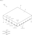
- FIG. 1 is a perspective view showing a semiconductor device according to a first embodiment of the present disclosure.
- FIG. 2 is a plan view (through a sealing resin) showing the semiconductor device according to the first embodiment of the present disclosure.
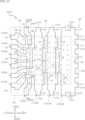
- FIG. 3 is a plan view (with a semiconductor element and a sealing resin transparent) showing the semiconductor device according to the first embodiment of the present disclosure.
- FIG. 4 is a bottom view showing the semiconductor device according to the first embodiment of the present disclosure.
- FIG. 5 is a front view showing the semiconductor device according to the first embodiment of the present disclosure.
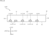
- FIG. 6 is a rear view showing the semiconductor device according to the first embodiment of the present disclosure.
- FIG. 7 is a right side view showing the semiconductor device according to the first embodiment of the present disclosure.
- FIG. 1 is a perspective view showing a semiconductor device according to a first embodiment of the present disclosure.
- FIG. 2 is a plan view (through a sealing resin) showing the semiconductor device according to the first embodiment of the present disclosure.
- FIG. 3 is a
- FIG. 8 is a left side view showing the semiconductor device according to the first embodiment of the present disclosure.
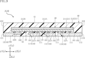
- FIG. 9 is a cross-sectional view taken along line IX-IX in FIG.
- FIG. 10 is a cross-sectional view taken along line XX in FIG.
- FIG. 11 is a cross-sectional view taken along line XI-XI in FIG.
- FIG. 12 is a cross-sectional view taken along line XII-XII in FIG.
- FIG. 13 is a partial enlarged view (near the first conductive columnar portion) of FIG.
- FIG. 14 is a partial enlarged view (near the second conductive columnar portion) of FIG.
- FIG. 15 is a cross-sectional view similar to FIG. 14, showing a semiconductor device according to a first modification of the first embodiment.
- FIG. 16 is a cross-sectional view similar to FIG. 14, showing a semiconductor device according to a second modification of the first embodiment.
- FIG. 17 is a plan view (with a semiconductor element and a sealing resin transparent) showing a semiconductor device according to a third modification of the first embodiment.
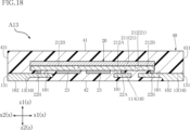
- FIG. 18 is a cross-sectional view taken along line XVIII-XVIII in FIG.
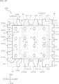
- FIG. 19 is a plan view (through a sealing resin) showing a semiconductor device according to a second embodiment of the present disclosure.
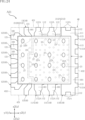
- FIG. 20 is a plan view (with a semiconductor element and a sealing resin transparent) showing a semiconductor device according to a second embodiment of the present disclosure.
- FIG. 21 is a cross-sectional view taken along line XXI-XXI in FIG. FIG.
- FIG. 22 is a cross-sectional view taken along line XXII-XXII in FIG.
- FIG. 23 is a cross-sectional view taken along line XXIII-XXIII in FIG.
- FIG. 24 is a plan view (through a sealing resin) showing a semiconductor device according to a first modification of the second embodiment.
- FIG. 25 is a plan view (with a semiconductor element and a sealing resin transparent) showing a semiconductor device according to a first modification of the second embodiment.
- FIG. 26 is a cross-sectional view taken along line XXVI-XXVI in FIG.
- FIG. 27 is a cross-sectional view taken along line XXVII-XXVII in FIG.
- FIG. 28 is a cross-sectional view taken along line XXVIII-XXVIII in FIG.
- an object A is formed on an object B" and “an object A is formed on an object B” include “an object A is formed directly on an object B” and “an object A is formed on an object B with another object interposed between the object A and the object B” unless otherwise specified.
- an object A is disposed on an object B” and “an object A is disposed on an object B” include “an object A is disposed directly on an object B” and “an object A is disposed on an object B with another object interposed between the object A and the object B" unless otherwise specified.
- an object A is located on an object B includes “an object A is located on an object B in contact with an object B” and “an object A is located on an object B with another object interposed between the object A and the object B” unless otherwise specified.
- an object A overlaps an object B when viewed in a certain direction includes “an object A overlaps the entire object B” and “an object A overlaps a part of an object B.”
- a surface A faces in direction B is not limited to the case where the angle of surface A with respect to direction B is 90°, but also includes the case where surface A is tilted with respect to direction B.
- the semiconductor device A10 includes a conductive member 10, a semiconductor element 20, a bonding layer 30, and a sealing resin 40.
- the package format of the semiconductor device A10 is a QFN (Quad For Non-Lead Package).
- the package format of the semiconductor device A10 is not limited to QFN.
- the semiconductor element 20 is a flip-chip type LSI.
- the semiconductor element 20 includes a switching circuit 212A and a control circuit 212B (each of which will be described in detail later). In the semiconductor device A10, the switching circuit 212A converts DC power (voltage) into AC power (voltage).
- the semiconductor device A10 is used as one element constituting a circuit of a DC/DC converter, for example.
- FIG. 1 is a perspective view of the semiconductor device A10.
- FIG. 2 is a plan view of the semiconductor device A10, seen through the sealing resin 40.
- FIG. 3 is a plan view of the semiconductor device A10, seen through the semiconductor element 20 and the sealing resin 40.
- FIG. 4 is a bottom view of the semiconductor device A10.
- FIG. 5 is a front view of the semiconductor device A10.
- FIG. 6 is a rear view of the semiconductor device A10.
- FIG. 7 is a right side view of the semiconductor device A10.
- FIG. 8 is a left side view of the semiconductor device A10.
- FIG. 9 is a cross-sectional view along line IX-IX in FIG. 3.
- FIG. 10 is a cross-sectional view along line X-X in FIG. 3.
- FIG. 9 is a cross-sectional view along line IX-IX in FIG. 3.
- FIG. 10 is a cross-sectional view along line X-X in FIG. 3.
- FIG. 9 is a cross-section
- FIG. 11 is a cross-sectional view along line XI-XI in FIG. 3.
- FIG. 12 is a cross-sectional view along line XII-XII in FIG. 3.
- FIGS. 13 and 14 are partial enlarged views of FIG. 12.
- the sealing resin 40 seen through is shown by an imaginary line (two-dot chain line).
- the semiconductor element 20 and the sealing resin 40 are shown by imaginary lines (double-dashed lines).
- the thickness direction of the conductive member 10 will be referred to as the "thickness direction z.”
- One direction orthogonal to the thickness direction z will be referred to as the "first direction x.”
- a direction orthogonal to both the thickness direction z and the first direction x will be referred to as the "second direction y.”
- the semiconductor device A10 is square-shaped when viewed in the thickness direction z (in a plan view).
- the conductive member 10 supports the semiconductor element 20 and serves as a terminal for mounting the semiconductor device A10 on a wiring board. As shown in FIGS. 9 to 12, a part of the conductive member 10 is covered with the sealing resin 40.
- the conductive member 10 has a main surface 101 and a back surface 102 that face opposite each other in the thickness direction z.
- the main surface 101 faces the z1 side in the thickness direction z and faces the semiconductor element 20.
- the semiconductor element 20 is supported by the main surface 101.
- the main surface 101 is covered with the sealing resin 40.
- the back surface 102 faces the other side in the thickness direction z.
- the conductive member 10 is composed of a single lead frame.
- the constituent material of the lead frame is, for example, copper (Cu) or a copper alloy.
- the conductive member 10 includes a plurality of leads 11A, 11B, 11C, a plurality of leads 12, and a pair of leads 13.
- the multiple leads 11A to 11C are strip-shaped extending in the second direction y when viewed in the thickness direction z.
- the multiple leads 11A to 11C are arranged along the second direction y.
- the multiple leads 11A to 11C are arranged in the order of lead 11A, lead 11C, lead 11C from the y1 side of the second direction y to the y2 side of the second direction y.
- the leads 11A and 11B are input terminals to which the DC power (voltage) to be converted in the semiconductor device A10 is input.
- the lead 11A is the positive electrode (P terminal).
- the lead 11B is the negative electrode (N terminal).
- the lead 11C is an output terminal to which the AC power (voltage) converted by the switching circuit 212A configured in the semiconductor element 20 is output.
- lead 11A is located between the multiple leads 12 and lead 11C in the second direction y.
- Lead 11C is located between lead 11A and lead 11B in the second direction y.
- Each of leads 11A to 11C includes a main portion 111 and a pair of side portions 112. As shown in FIGS. 3 and 4, main portion 111 extends in the first direction x.
- the semiconductor element 20 is supported on the main surface 101 of main portion 111.
- the pair of side portions 112 are connected to both ends of main portion 111 in the first direction x.
- each of the pair of side portions 112 has an end surface 112A.
- the end surface 112A is connected to both main surface 101 and back surface 102 of leads 11A to 11C and faces the first direction x.
- the end surface 112A is exposed from the sealing resin 40.
- lead 11B is located on the y2 side of lead 11C in the second direction y. Therefore, lead 11B is located on the y2 side of the multiple leads 11A to 11C in the second direction y.
- Lead 11B includes a main portion 111, a pair of side portions 112, and multiple protrusions 113.
- the multiple protrusions 113 protrude from the y2 side of the main portion 111 in the second direction y.
- Sealing resin 40 is filled between two adjacent protrusions 113.
- each of the multiple protrusions 113 has a minor end surface 113A.
- the minor end surface 113A is connected to both the main surface 101 and the back surface 102 of lead 11B and faces the y2 side in the second direction y.
- the minor end surface 113A is exposed from the sealing resin 40.
- the multiple minor end surfaces 113A are arranged at a predetermined interval along the first direction x.
- a notch 112B is formed in each of a pair of side portions 112 of lead 11B.
- the notch 112B extends from the main surface 101 to the back surface 102 of lead 11B, and is recessed in the first direction x from the end surface 112A. This divides the end surface 112A into two regions spaced apart from each other in the second direction y.
- the notch 112B is filled with sealing resin 40.
- the area of the main surface 101 of each of the multiple leads 11A to 11C is larger than the area of the back surface 102.
- the areas of the back surfaces 102 of each of leads 11A and 11C are equal.
- the area of the back surface 102 of lead 11B is larger than the area of the back surfaces 102 of each of leads 11A and 11C.
- the main surface 101 of the main portion 111 on which the semiconductor element 20 is supported may be plated with, for example, silver (Ag).
- the back surface 102 exposed from the sealing resin 40, the pair of end faces 112A, and the multiple minor end faces 113A may be plated with, for example, tin (Sn).
- tin plating multiple metal platings may be used, for example, layered in the order of nickel (Ni), palladium (Pd), and gold (Au).
- the multiple leads 12 are located on the y1 side of the multiple leads 11A to 11C in the second direction y.
- One of the multiple leads 12 is a ground terminal of the control circuit 212B configured in the semiconductor element 20.
- power (voltage) for driving the control circuit 212B or an electrical signal to be transmitted to the control circuit 212B is input.
- each of the multiple leads 12 has an end face 121.
- the end face 121 is connected to both the main surface 101 and the back surface 102 of the lead 12 and faces the y1 side in the second direction y.
- the end face 121 is exposed from the sealing resin 40.
- the multiple end faces 121 are arranged at a predetermined interval along the first direction x.
- the area of the main surface 101 of each of the multiple leads 12 is larger than the area of the back surface 102.
- the areas of the back surfaces 102 of the multiple leads 12 are all equal.
- the main surfaces 101 of the multiple leads 12 on which the semiconductor element 20 is supported may be plated with silver, for example.
- the back surfaces 102 and end faces 121 of the multiple leads 12 exposed from the sealing resin 40 may be plated with tin, for example.
- tin plating multiple metal platings may be used, for example, layered in this order of nickel, palladium, and gold.
- each of the pair of leads 13 has an end face 131.
- the end face 131 is connected to both the main surface 101 and the back surface 102, and faces the first direction x.
- the end face 131 is exposed from the sealing resin 40.
- the end face 131 is arranged along the second direction y together with the end faces 112A of the multiple leads 11A to 11C.
- the area of the main surface 101 of each of the pair of leads 13 is larger than the area of the back surface 102.
- the main surface 101 of the pair of leads 13 on which the semiconductor element 20 is supported may be plated with silver, for example.
- the back surface 102 and end surface 131 of the pair of leads 13 exposed from the sealing resin 40 may be plated with tin, for example.
- tin plating multiple metal platings may be used, for example, layered in this order of nickel, palladium, and gold.
- the semiconductor element 20 is electrically connected to and supported by the conductive member 10 (plurality of leads 11A to 11C, multiple leads 12, and a pair of leads 13) by flip-chip bonding.
- the semiconductor element 20 is covered with a sealing resin 40.
- the semiconductor element 20 has an element body 21, multiple first conductive columnar portions 22A, multiple first conductive columnar portions 22B, multiple second conductive columnar portions 23, and an insulating film 25.
- the element body 21 forms the main part of the semiconductor element 20. As shown in Figures 13 and 14, the element body 21 has a semiconductor substrate 211, a semiconductor layer 212, and a passivation film 213.
- the semiconductor substrate 211 supports below it a semiconductor layer 212, a passivation film 213, a plurality of first conductive columnar sections 22A, a plurality of first conductive columnar sections 22B, a plurality of second conductive columnar sections 23, a plurality of conductive pads 24, and an insulating film 25.
- the constituent material of the semiconductor substrate 211 is, for example, Si (silicon) or silicon carbide (SiC).
- the semiconductor layer 212 is laminated on the side of the semiconductor substrate 211 facing the main surface 101 of the conductive member 10.
- the semiconductor layer 212 includes multiple types of p-type and n-type semiconductors based on differences in the amount of elements to be doped.
- the semiconductor layer 212 includes a switching circuit 212A and a control circuit 212B that is conductive to the switching circuit 212A.
- the switching circuit 212A is a MOSFET (Metal-Oxide-Semiconductor Field-Effect Transistor) or an IGBT (Insulated Gate Bipolar Transistor), for example.
- the switching circuit 212A is divided into two regions, a high-voltage region (upper arm circuit) and a low-voltage region (lower arm circuit). Each region is composed of one n-channel MOSFET.
- the control circuit 212B includes a gate driver for driving the switching circuit 212A, a bootstrap circuit corresponding to the high voltage region of the switching circuit 212A, and the like, and performs control for driving the switching circuit 212A normally.
- a wiring layer (not shown) is formed in the semiconductor layer 212.
- the switching circuit 212A and the control circuit 212B are mutually conductive through the wiring layer.
- the passivation film 213 covers the lower surface of the semiconductor layer 212.
- the passivation film 213 has electrical insulation properties.
- the passivation film 213 is composed of, for example, a silicon oxide film (SiO 2 ) in contact with the lower surface of the semiconductor layer 212, and a silicon nitride film (Si 3 N 4 ) laminated on the silicon oxide film.
- the passivation film 213 is provided with a plurality of openings 213A penetrating in the thickness direction z.
- the multiple first conductive columnar portions 22A and the multiple first conductive columnar portions 22B are interposed between the element body 21 and the main surface 101 of the conductive member 10 in the thickness direction z.
- the multiple first conductive columnar portions 22A and the multiple first conductive columnar portions 22B protrude from the side of the element body 21 facing the main surface 101 of the conductive member 10 toward the main surface 101 of the conductive member 10.
- the upper ends of the multiple first conductive columnar portions 22A and the multiple first conductive columnar portions 22B are conductive to the semiconductor layer 212 of the element body 21.
- the multiple first conductive columnar portions 22A and the multiple first conductive columnar portions 22B are electrically connected to the main surface 101 of the conductive member 10.
- the multiple first conductive columnar portions 22A and the multiple first conductive columnar portions 22B function as so-called electrodes in the semiconductor element 20.
- the multiple first conductive columnar portions 22A are electrically connected to the switching circuit 212A of the semiconductor layer 212.
- the multiple first conductive columnar portions 22A are electrically connected to the main surfaces 101 of the multiple leads 11A to 11C.
- the multiple leads 11A to 11C are electrically connected to the switching circuit 212A.
- the multiple first conductive columnar portions 22B are electrically connected to the control circuit 212B of the semiconductor layer 212.
- most of the multiple first conductive columnar portions 22B are electrically connected to the main surfaces 101 of the multiple leads 12.
- the remaining first conductive columnar portions 22B are electrically connected to the main surfaces 101 of the pair of leads 13. As a result, the multiple leads 12 and the pair of leads 13 are electrically connected to the control circuit 212B.
- each of the multiple first conductive columnar portions 22A and the multiple first conductive columnar portions 22B is electrically connected to the semiconductor layer 212 of the element body 21 through one of the multiple conductive pads 24.
- the multiple conductive pads 24 are arranged on the z2 side of the semiconductor layer 212 in the thickness direction z and are in contact with the semiconductor layer 212. As a result, each of the multiple conductive pads 24 is electrically connected to one of the switching circuit 212A and the control circuit 212B of the semiconductor layer 212.
- the conductive pad 24 is made of a material that includes aluminum (Al) or copper. Alternatively, the conductive pad 24 may be made of multiple metal layers that are stacked in this order from the semiconductor layer 212 downward, including copper, nickel, and palladium.
- the conductive pad 24 is in contact with the passivation film 213 of the element body 21. A part of the conductive pad 24 is exposed from the opening 213A of the passivation film 213.
- the first conductive columnar portions 22A and 22B protrude from the portion of the conductive pad 24 exposed from the opening 213A toward the main surface 101 of the conductive member 10.
- the first conductive columnar portions 22A and 22B are, for example, cylindrical.
- the constituent material of the first conductive columnar portions 22A and 22B includes, for example, copper.
- the multiple first conductive columnar portions 22A and the multiple first conductive columnar portions 22B are made of, for example, metal plating.
- the tip 221 of the first conductive columnar portion 22A, 22B has a tip surface 221A and a side surface 221B.
- the tip surface 221A faces the main surface 101 of the conductive member 10.
- the side surface 221B is connected to the tip surface 221A and faces a direction perpendicular to the thickness direction z.
- the tip surface 221A of the first conductive columnar portion 22A, 22B is flat and parallel to the main surface 101 of the conductive member 10.
- the tip surface 221A of the first conductive columnar portion 22A, 22B may be concave toward the element body 21, or may be convex toward the main surface 101 of the conductive member 10.
- the multiple first conductive columnar portions 22A and the multiple first conductive columnar portions 22B are formed, for example, by electrolytic plating.
- the insulating film 25 covers the side of the element body 21 facing the main surface 101 of the conductive member 10, i.e., the passivation film 213 located on the z2 side of the element body 21 in the thickness direction z.
- the insulating film 25 protects the surface of the element body 21 facing the main surface 101 of the conductive member 10.
- a portion of each of the multiple conductive pads 24 is exposed from the insulating film 25.
- the insulating film 25 is spaced apart from the multiple first conductive columnar portions 22A and the multiple first conductive columnar portions 22B.
- the insulating film 25 has multiple openings 251 penetrating in the thickness direction z.
- the first conductive columnar portions 22A, 22B are exposed from any of the multiple openings 251.
- the tip surface 221A of the first conductive columnar portions 22A and 22B is located between the main surface 101 of the conductive member 10 and the insulating film 25 in the thickness direction z.
- the insulating film 25 has electrical insulation properties.
- the insulating film 25 is made of, for example, polyimide.
- the bonding layer 30 contacts both the main surface 101 of the conductive member 10 and the multiple first conductive columnar portions 22A and the multiple first conductive columnar portions 22B.
- the bonding layer 30 is conductive.
- the multiple first conductive columnar portions 22A and the multiple first conductive columnar portions 22B are electrically connected to the main surface 101 of the conductive member 10.
- the bonding layer 30 is, for example, solder (a metal containing tin and silver).
- solder a metal containing tin and silver
- the second conductive columnar parts 23 are arranged on the element body 21.
- the second conductive columnar parts 23 protrude from the side of the element body 21 facing the main surface 101 of the conductive member 10 toward the z2 side in the thickness direction z.
- each of the second conductive columnar parts 23 does not overlap with the main surface 101 of the conductive member 10 in the thickness direction z.
- the second conductive columnar parts 23 are arranged in three regions between the lead 11A and the leads 12, between the lead 11C and the lead 11A, and between the lead 11B and the lead 11C in the thickness direction z. In each of these regions, the second conductive columnar parts 23 are arranged at intervals in the first direction x.
- the upper ends of the multiple second conductive columnar portions 23 are electrically connected to the semiconductor layer 212 of the element body 21 via the conductive pads 24. As shown in FIGS. 9, 12, and 14, the multiple second conductive columnar portions 23 are electrically connected to the switching circuit 212A or the control circuit 212B of the semiconductor layer 212.
- each of the multiple second conductive columnar parts 23 is electrically connected to the semiconductor layer 212 of the element body 21 via one of the multiple conductive pads 24.
- the second conductive columnar part 23 protrudes toward the z2 side in the thickness direction z from the portion of the conductive pad 24 exposed from the opening 213A of the passivation film 213.
- the second conductive columnar part 23 is, for example, cylindrical.
- the area of the second conductive columnar part 23 as viewed in the thickness direction z is approximately the same as the area of each of the multiple first conductive columnar parts 22A and the multiple first conductive columnar parts 22B as viewed in the thickness direction z.
- the material of the second conductive columnar part 23 includes, for example, copper.
- the material of the second conductive columnar part 23 is the same as the material of the first conductive columnar parts 22A and 22B.
- the multiple second conductive columnar parts 23 are, for example, made of metal plating.
- At least the tip 231 of the second conductive columnar portion 23 is in contact with the sealing resin 40 and is covered by the sealing resin 40. Therefore, each of the multiple second conductive columnar portions 23 is not electrically connected to the conductive member 10.
- the tip 231 of the second conductive columnar portion 23 has a tip surface 231A and a side surface 231B.
- the tip surface 231A of the second conductive columnar portion 23 is flat and parallel to the main surface 101 of the conductive member 10.
- the side surface 231B is connected to the tip surface 231A and faces in a direction perpendicular to the thickness direction z.
- the second conductive columnar portion 23 may be concave toward the element body 21, or may be convex toward the z2 side of the thickness direction z.
- the multiple second conductive columnar portions 23 are formed, for example, by electrolytic plating.
- the second conductive columnar portion 23 is exposed from one of a plurality of openings 251 provided in the insulating film 25.
- the tip surface 231A of the second conductive columnar portion 23 is located between the main surface 101 of the conductive member 10 and the insulating film 25 in the thickness direction z.
- the tip surface 231A of the second conductive columnar portion 23 is located at the same position as the tip surfaces 221A of the first conductive columnar portions 22A, 22B in the thickness direction z.
- the sealing resin 40 has a resin main surface 41, a resin back surface 42, a pair of first resin side surfaces 431, and a pair of second resin side surfaces 432.
- the constituent material of the sealing resin 40 is, for example, a black epoxy resin.
- the resin main surface 41 faces the same side as the main surface 101 of the conductive member 10 in the thickness direction z.
- the resin main surface 41 faces the z1 side in the thickness direction z.
- the resin back surface 42 faces the opposite side to the resin main surface 41.
- the resin back surface 42 faces the z2 side in the thickness direction z.
- the back surfaces 102 of the multiple leads 11A to 11C, the back surfaces 102 of the multiple leads 12, and the back surfaces 102 of a pair of leads 13 are exposed from the resin back surface 42.
- the pair of first resin side surfaces 431 are connected to both the resin main surface 41 and the resin back surface 42, and face the first direction x.
- the pair of first resin side surfaces 431 are spaced apart from each other in the second direction y.
- the end faces 112A of the multiple leads 11A to 11C and the end face 131 of the lead 13 are exposed from each of the pair of first resin side surfaces 431 so as to be flush with the first resin side surfaces 431.
- the pair of second resin side surfaces 432 are connected to all of the resin main surface 41, the resin back surface 42, and the pair of first resin side surfaces 431, and face the second direction y.
- the pair of second resin side surfaces 432 are spaced apart from each other in the first direction x.
- the end faces 121 of the multiple leads 12 are exposed from the second resin side surface 432 located on the y1 side of the second direction y so as to be flush with the second resin side surface 432.
- the multiple minor end faces 113A of the lead 11B are exposed from the second resin side surface 432 located on the y2 side of the second direction y so as to be flush with the second resin side surface 432.
- the semiconductor device A10 includes a conductive member 10 having a main surface 101, a semiconductor element 20 disposed on the z2 side of the conductive member 10 in the thickness direction z and supported by the main surface 101, and a sealing resin 40 covering a part of the conductive member 10 and the semiconductor element 20.
- the semiconductor element 20 has an element body 21, a plurality of first conductive columnar portions 22A, a plurality of first conductive columnar portions 22B, and a plurality of second conductive columnar portions 23.
- the plurality of first conductive columnar portions 22A and the plurality of first conductive columnar portions 22B protrude from the element body 21 to the z2 side in the thickness direction z, and are interposed between the element body 21 and the main surface 101 of the conductive member 10 in the thickness direction z.
- Each of the plurality of first conductive columnar portions 22A and the plurality of first conductive columnar portions 22B is electrically connected to both the element body 21 and the main surface 101.
- Each of the second conductive columnar parts 23 is disposed on the element body 21 and protrudes in the thickness direction z.
- the tip 231 of each of the second conductive columnar parts 23 is in contact with the sealing resin 40 and is covered by the sealing resin 40.
- each of the second conductive columnar parts 23 is not electrically connected to the conductive member 10.
- the second conductive columnar parts 23 do not form a path for a current flowing through the semiconductor element 20 inside the semiconductor device A10.
- the heat generated in the semiconductor element 20 is dissipated by being transmitted to the first conductive columnar parts 22A and 22B and the conductive member 10, and is also transmitted to the second conductive columnar parts 23. Therefore, the semiconductor device A10 can improve the heat dissipation of the heat generated in the semiconductor element 20.
- the multiple second conductive columnar portions 23 protrude from the element body 21 toward the z2 side in the thickness direction z.
- the multiple second conductive columnar portions 23 do not overlap with the main surface 101 of the conductive member 10 when viewed in the thickness direction z.
- the constituent material of the second conductive columnar portions 23 is the same as the constituent material of the first conductive columnar portions 22A, 22B. With this configuration, the multiple second conductive columnar portions 23 can be formed collectively on the z2 side of the element body 21 in the thickness direction z together with the multiple first conductive columnar portions 22A, 22B.
- Each of the multiple second conductive columnar portions 23 is in contact with one of the multiple conductive pads 24 and protrudes from the conductive pad 24 to the z2 side in the thickness direction z. With this configuration, heat generated in the semiconductor element 20 can be efficiently dissipated to the second conductive columnar portion 23 via the conductive pad 24. This is preferable in terms of improving the heat dissipation properties of the semiconductor device A10.
- FIGS. 15 to 18 show modified examples of the semiconductor device A10 according to the first embodiment.
- elements that are the same as or similar to those in the above embodiment are given the same reference numerals as in the above embodiment, and duplicated descriptions are omitted.
- Fig. 15 shows a semiconductor device A11 according to a first modification of the first embodiment.
- Fig. 15 is a cross-sectional view of the semiconductor device A11, and is an enlarged cross-sectional view of the vicinity of the second conductive columnar portion 23, similar to Fig. 14.
- the semiconductor device A11 differs from the above embodiment in the arrangement of the second conductive columnar portion 23 on the element body 21.
- the semiconductor element 20 further includes a metal layer 26.
- the metal layer 26 is laminated on the insulating film 25.
- the constituent material of the metal layer 26 includes, for example, copper.
- the metal layer 26 is, for example, made of metal plating.
- the metal layer 26 is laminated across the surface of the conductive pad 24 facing the z2 side in the thickness direction z and the surface of the insulating film 25 facing the z2 side in the thickness direction z.
- the metal layer 26 includes a first portion 261.
- the first portion 261 is a portion that is laminated on the conductive pad 24 and is in contact with the conductive pad 24.
- the second conductive columnar portion 23 is disposed on the metal layer 26 and protrudes from the metal layer 26 to the z2 side in the thickness direction z.
- the second conductive columnar portion 23 is electrically connected to the conductive pad 24 via the first portion 261.
- each of the multiple second conductive columnar parts 23 is disposed on the element body 21 and protrudes in the thickness direction z.
- the tip 231 of each of the multiple second conductive columnar parts 23 is in contact with the sealing resin 40 and is covered by the sealing resin 40.
- each of the multiple second conductive columnar parts 23 is not electrically connected to the conductive member 10.
- the multiple second conductive columnar parts 23 do not form a path for current flowing through the semiconductor element 20 inside the semiconductor device A11.
- the semiconductor device A11 can improve the heat dissipation performance of heat generated in the semiconductor element 20.
- Each of the multiple second conductive columnar portions 23 is electrically connected to the conductive pad 24 via the metal layer 26 (first portion 261) that contacts the conductive pad 24.
- heat generated in the semiconductor element 20 can be efficiently dissipated to the second conductive columnar portion 23 via the conductive pad 24 and the metal layer 26. This is preferable in terms of improving the heat dissipation properties of the semiconductor device A11.
- the semiconductor device A11 achieves the same effects as the semiconductor device A10 within the same range of configuration as the semiconductor device A10 of the above embodiment.
- Fig. 16 shows a semiconductor device A12 according to a second modification of the first embodiment.
- Fig. 16 is a cross-sectional view of the semiconductor device A12, and is an enlarged cross-sectional view of the vicinity of the second conductive columnar portion 23, similar to Fig. 14.
- the semiconductor device A12 differs from the above embodiment in the arrangement of the second conductive columnar portion 23 on the element body 21.
- the semiconductor element 20 has a metal layer 26, similar to the semiconductor device A11.
- the metal layer 26 is formed by laminating on the insulating film 25.
- the constituent material of the metal layer 26 includes, for example, copper.
- the metal layer 26 is formed, for example, by metal plating.
- the metal layer 26 includes a second portion 262.
- the second portion 262 is laminated on the surface of the insulating film 25 facing the z2 side in the thickness direction z, and is not in contact with any of the multiple conductive pads 24.
- the second conductive columnar portion 23 is disposed on the second portion 262 and protrudes from the second portion 262 to the z2 side in the thickness direction z.
- each of the multiple second conductive columnar parts 23 is disposed on the element body 21 and protrudes in the thickness direction z.
- the tip 231 of each of the multiple second conductive columnar parts 23 is in contact with the sealing resin 40 and is covered by the sealing resin 40.
- each of the multiple second conductive columnar parts 23 is not electrically connected to the conductive member 10.
- the multiple second conductive columnar parts 23 do not form a path for current flowing through the semiconductor element 20 inside the semiconductor device A12.
- the semiconductor device A12 can improve the heat dissipation performance of heat generated in the semiconductor element 20.
- Each of the multiple second conductive columnar portions 23 is disposed on the metal layer 26 (second portion 262).
- the second portion 262 is not in contact with any of the multiple conductive pads 24.
- This configuration increases the degree of freedom in arranging the multiple second conductive columnar portions 23.
- the semiconductor device A12 achieves the same effects as the semiconductor device A10 within the same range of configuration as the semiconductor device A10 of the above embodiment.
- Figures 17 and 18 show a semiconductor device A13 according to a third modified example of the first embodiment.
- Figure 17 is a plan view of the semiconductor device A13, with the semiconductor element 20 and the sealing resin 40 seen through.
- Figure 18 is a cross-sectional view taken along line XVIII-XVIII in Figure 17.
- the semiconductor element 20 and the sealing resin 40 seen through are respectively indicated by imaginary lines (two-dot chain lines).
- the semiconductor device A13 differs from the above embodiment in the shape of the multiple second conductive columnar portions 23 when viewed in the thickness direction z.
- each of the multiple second conductive columnar portions 23 is elongated in the first direction x when viewed in the thickness direction z.
- the area of the second conductive columnar portion 23 when viewed in the thickness direction z is larger than the area of each of the multiple first conductive columnar portions 22A and the multiple first conductive columnar portions 22B when viewed in the thickness direction z.
- each of the multiple second conductive columnar parts 23 is disposed on the element body 21 and protrudes in the thickness direction z.
- the tip 231 of each of the multiple second conductive columnar parts 23 is in contact with the sealing resin 40 and is covered by the sealing resin 40.
- each of the multiple second conductive columnar parts 23 is not electrically connected to the conductive member 10.
- the multiple second conductive columnar parts 23 do not form a path for a current flowing through the semiconductor element 20 inside the semiconductor device A13.
- the heat generated in the semiconductor element 20 is dissipated by being transmitted to the multiple first conductive columnar parts 22A, 22B and the conductive member 10, and is also transmitted to the multiple second conductive columnar parts 23. Therefore, the semiconductor device A13 can improve the heat dissipation of heat generated in the semiconductor element 20.
- the area of the second conductive columnar portion 23 as viewed in the thickness direction z is larger than the area of each of the multiple first conductive columnar portions 22A and the multiple first conductive columnar portions 22B as viewed in the thickness direction z.
- the semiconductor device A13 achieves the same effects as the semiconductor device A10 within the same range of configuration as the semiconductor device A10 of the above embodiment.
- Second embodiment 19 to 23 show a semiconductor device A20 according to a second embodiment of the present disclosure.
- elements that are the same as or similar to those in the above embodiment are given the same reference numerals as in the above embodiment, and duplicated descriptions are omitted.
- FIG. 19 is a plan view of the semiconductor device A20, seen through the sealing resin 40.
- FIG. 20 is a plan view of the semiconductor device A20, seen through the semiconductor element 20 and the sealing resin 40.
- FIG. 21 is a cross-sectional view taken along line XXI-XXI in FIG. 20.
- FIG. 22 is a cross-sectional view taken along line XXII-XXII in FIG. 20.
- FIG. 23 is a cross-sectional view taken along line XXIII-XXIII in FIG. 20.
- the see-through sealing resin 40 is shown by an imaginary line (two-dot chain line).
- the see-through semiconductor element 20 and sealing resin 40 are each shown by an imaginary line (two-dot chain line).
- the semiconductor element 20 has a plurality of second conductive columnar portions 27 instead of the plurality of second conductive columnar portions 23 of the above embodiment.
- Each of the plurality of second conductive columnar portions 27 protrudes from the element body 21 toward the z1 side in the thickness direction z.
- the plurality of second conductive columnar portions 27 are arranged on the top surface 211A (the surface facing the z1 side in the thickness direction z) of the semiconductor substrate 211 constituting the element body 21. As shown in Figures 20 to 22, each of the plurality of second conductive columnar portions 27 may overlap the main surface 101 of the conductive member 10 when viewed in the thickness direction z.
- the arrangement of the plurality of second conductive columnar portions 27 is not particularly limited, and in the illustrated example, the plurality of second conductive columnar portions 27 are arranged at intervals in both the first direction x and the second direction y.
- the tip of each of the multiple second conductive columnar sections 27 (the end on the z1 side in the thickness direction z) is in contact with the sealing resin 40 and is covered by the sealing resin 40.
- the second conductive columnar portion 27 is, for example, a columnar portion having an elliptical cross section. As shown in FIG. 19 and FIG. 20, the area of the second conductive columnar portion 27 as viewed in the thickness direction z is larger than the area of each of the first conductive columnar portions 22A and the first conductive columnar portions 22B as viewed in the thickness direction z.
- the material of the second conductive columnar portion 27 includes, for example, copper.
- the second conductive columnar portions 27 are made of, for example, metal plating.
- the second conductive columnar portions 27 are formed by, for example, electrolytic plating.
- a conductive base layer is formed in a predetermined region of the top surface 211A (the surface facing the z1 side in the thickness direction z) of the semiconductor substrate 211, and the second conductive columnar portion 27 is formed on the base layer.
- the dimension of the second conductive columnar portion 27 in the thickness direction z is larger than the dimension of the first conductive columnar portions 22A and 22B in the thickness direction z.
- the semiconductor device A20 includes a conductive member 10 having a main surface 101, a semiconductor element 20 disposed on the z2 side of the conductive member 10 in the thickness direction z and supported by the main surface 101, and a sealing resin 40 covering a part of the conductive member 10 and the semiconductor element 20.
- the semiconductor element 20 has an element body 21, a plurality of first conductive columnar portions 22A, a plurality of first conductive columnar portions 22B, and a plurality of second conductive columnar portions 27.
- the plurality of first conductive columnar portions 22A and the plurality of first conductive columnar portions 22B protrude from the element body 21 to the z2 side in the thickness direction z, and are interposed between the element body 21 and the main surface 101 of the conductive member 10 in the thickness direction z.
- Each of the plurality of first conductive columnar portions 22A and the plurality of first conductive columnar portions 22B is electrically connected to both the element body 21 and the main surface 101.
- Each of the second conductive columnar parts 27 is disposed on the element body 21 and protrudes in the thickness direction z. The tip of each of the second conductive columnar parts 27 is in contact with the sealing resin 40 and is covered by the sealing resin 40.
- each of the second conductive columnar parts 27 is not electrically connected to the conductive member 10.
- the second conductive columnar parts 27 do not form a path for a current flowing through the semiconductor element 20 inside the semiconductor device A20.
- the heat generated in the semiconductor element 20 is dissipated by being transmitted to the first conductive columnar parts 22A and 22B and the conductive member 10, and is also transmitted to the second conductive columnar parts 27. Therefore, the semiconductor device A20 can improve the heat dissipation of the heat generated in the semiconductor element 20.
- the second conductive columnar portions 27 protrude from the element body 21 toward the z1 side in the thickness direction z, which is the opposite side to the conductive member 10. This allows the second conductive columnar portions 27 to be arranged so as to overlap the main surface 101 of the conductive member 10 when viewed in the thickness direction z, thereby increasing the freedom of arrangement. Specifically, as in the illustrated example, the second conductive columnar portions 27 can be arranged so as to overlap the main surface 101 of the conductive member 10 when viewed in the thickness direction z.
- the dimension of the second conductive columnar portion 27 in the thickness direction z can be made larger than the dimension of the first conductive columnar portions 22A and 22B in the thickness direction z. This is preferable in terms of improving the heat dissipation of the semiconductor device A20.
- First modified example 24 to 28 show a semiconductor device A21 according to a first modified example of the second embodiment.
- elements that are the same as or similar to those in the above embodiment are given the same reference numerals as in the above embodiment, and duplicated explanations will be omitted.
- FIG. 24 is a plan view of the semiconductor device A21, seen through the sealing resin 40.
- FIG. 25 is a plan view of the semiconductor device A21, seen through the semiconductor element 20 and the sealing resin 40.
- FIG. 26 is a cross-sectional view taken along line XXVI-XXVI in FIG. 25.
- FIG. 27 is a cross-sectional view taken along line XXVII-XXVII in FIG. 25.
- FIG. 28 is a cross-sectional view taken along line XXVIII-XXVIII in FIG. 25.
- the see-through sealing resin 40 is shown by an imaginary line (two-dot chain line).
- the see-through semiconductor element 20 and sealing resin 40 are each shown by an imaginary line (two-dot chain line).
- the semiconductor element 20 has a plurality of second conductive columnar portions 23 in addition to a plurality of second conductive columnar portions 27.
- the plurality of second conductive columnar portions 27 have the same configuration as the semiconductor device A20 of the above embodiment.
- the plurality of second conductive columnar portions 23 have the same configuration as the semiconductor device A10 of the above first embodiment.
- each of the multiple second conductive columnar portions 23 and the multiple second conductive columnar portions 27 is disposed on the element body 21 and protrudes in the thickness direction z.
- the tip of each of the multiple second conductive columnar portions 23 and the multiple second conductive columnar portions 27 is in contact with the sealing resin 40 and is covered by the sealing resin 40.
- each of the multiple second conductive columnar portions 23 and the multiple second conductive columnar portions 27 is not conductive to the conductive member 10.
- the multiple second conductive columnar portions 23 and the multiple second conductive columnar portions 27 do not form a path for current flowing through the semiconductor element 20 inside the semiconductor device A21.
- the semiconductor device A21 can improve the dissipation of heat generated in the semiconductor element 20.
- the semiconductor element 20 has a plurality of second conductive columnar portions 23 and a plurality of second conductive columnar portions 27, so that heat generated in the semiconductor element 20 can be dissipated to both sides in the thickness direction z. This is preferable in terms of improving the heat dissipation properties of the semiconductor device A21.
- the semiconductor device A21 achieves the same effects as the semiconductor devices A10 and A20 within the same range of configuration as the semiconductor devices A10 and A20 of the above embodiment.
- the semiconductor device according to the present disclosure is not limited to the above-mentioned embodiment.
- the specific configuration of each part of the semiconductor device according to the present disclosure can be freely designed in various ways.
- the conductive member 10 is described as being composed of multiple leads 11A-11C, multiple leads 12, and a pair of leads 13, but the present disclosure is not limited to this.
- the conductive member 10 may be composed of, for example, metal plating of a desired shape.
- a conductive member having a main surface facing one side in a thickness direction; a semiconductor element disposed on one side of the conductive member in the thickness direction and supported by the main surface; a sealing resin that covers a portion of the conductive member and the semiconductor element,
- the semiconductor element includes an element body, a plurality of first conductive columnar portions, and at least one second conductive columnar portion; each of the plurality of first conductive columnar portions is interposed between the element body and the main surface in the thickness direction and is electrically connected to the element body and the main surface;
- Each of the at least one second conductive columnar portion is disposed on the element body and protrudes in the thickness direction; a tip portion in the thickness direction of each of the at least one second conductive columnar portion is covered with the sealing resin.
- Appendix 2 The semiconductor device of claim 1, wherein at least one of the at least one second conductive columnar portions protrudes from the element body to the other side in the thickness direction and does not overlap with the main surface when viewed in the thickness direction.
- the element body includes a semiconductor substrate, a semiconductor layer stacked on the other side of the semiconductor substrate in the thickness direction, and a plurality of conductive pads arranged on the other side of the semiconductor layer in the thickness direction; 3.
- each of the first conductive columnar portions is electrically connected to one of the conductive pads. Appendix 4. 4.
- the semiconductor device wherein at least one of the plurality of first conductive columnar portions is in contact with the conductive pad and protrudes from the conductive pad to the other side in the thickness direction.
- Appendix 5. The semiconductor device according to claim 3, wherein at least one of the at least one second conductive columnar portion is in contact with the conductive pad and protrudes from the conductive pad to the other side in the thickness direction.
- Appendix 6. the semiconductor element has an insulating film covering the other side of the element body in the thickness direction, 6.
- the semiconductor device according to claim 3, wherein at least a portion of each of the plurality of conductive pads is exposed from the insulating film.
- Appendix 7. the semiconductor element has a metal layer formed on the insulating film; 7.
- the metal layer includes a first portion in contact with at least one of the plurality of conductive pads; 8. The semiconductor device according to claim 7, wherein at least one of the at least one second conductive columnar portion is electrically connected to the conductive pad via the first portion.
- Appendix 9. the metal layer includes a second portion that does not contact any of the plurality of conductive pads; The semiconductor device according to claim 7 or 8, wherein at least one of the at least one second conductive columnar portion is disposed on the second portion. Appendix 10. 10.
- a constituent material of the at least one second conductive columnar portion is the same as a constituent material of the plurality of first conductive columnar portions.
- Appendix 11 The conductive member has a back surface facing the opposite side in the thickness direction, the sealing resin has a resin main surface facing one side in the thickness direction and a resin back surface facing the other side in the thickness direction, 11. The semiconductor device according to claim 1, wherein the back surface is exposed from the resin back surface.
- Appendix 12. 12 The semiconductor device according to claim 11, wherein a constituent material of the conductive member includes copper.
- Appendix 13 13.
- the semiconductor device according to claim 11, wherein the conductive member is a lead. Appendix 14. 2.
- Appendix 15. A semiconductor device according to any one of claims 1 to 14, wherein the area of at least one of the at least one second conductive columnar portions as viewed in the thickness direction is larger than the area of each of the multiple first conductive columnar portions as viewed in the thickness direction. Appendix 16. 5. The semiconductor device according to claim 1, wherein at least one of the at least one second conductive columnar portion protrudes from the element body to one side in the thickness direction.
Landscapes
- Structures Or Materials For Encapsulating Or Coating Semiconductor Devices Or Solid State Devices (AREA)
Priority Applications (1)
| Application Number | Priority Date | Filing Date | Title |
|---|---|---|---|
| JP2024573006A JPWO2024157863A1 (https=) | 2023-01-24 | 2024-01-18 |
Applications Claiming Priority (2)
| Application Number | Priority Date | Filing Date | Title |
|---|---|---|---|
| JP2023-008846 | 2023-01-24 | ||
| JP2023008846 | 2023-01-24 |
Publications (1)
| Publication Number | Publication Date |
|---|---|
| WO2024157863A1 true WO2024157863A1 (ja) | 2024-08-02 |
Family
ID=91970559
Family Applications (1)
| Application Number | Title | Priority Date | Filing Date |
|---|---|---|---|
| PCT/JP2024/001205 Ceased WO2024157863A1 (ja) | 2023-01-24 | 2024-01-18 | 半導体装置 |
Country Status (2)
| Country | Link |
|---|---|
| JP (1) | JPWO2024157863A1 (https=) |
| WO (1) | WO2024157863A1 (https=) |
Citations (2)
| Publication number | Priority date | Publication date | Assignee | Title |
|---|---|---|---|---|
| JP2014056925A (ja) * | 2012-09-12 | 2014-03-27 | Shinko Electric Ind Co Ltd | 半導体パッケージ、半導体装置及び半導体パッケージの製造方法 |
| JP2020077723A (ja) * | 2018-11-07 | 2020-05-21 | ローム株式会社 | 半導体装置 |
-
2024
- 2024-01-18 JP JP2024573006A patent/JPWO2024157863A1/ja active Pending
- 2024-01-18 WO PCT/JP2024/001205 patent/WO2024157863A1/ja not_active Ceased
Patent Citations (2)
| Publication number | Priority date | Publication date | Assignee | Title |
|---|---|---|---|---|
| JP2014056925A (ja) * | 2012-09-12 | 2014-03-27 | Shinko Electric Ind Co Ltd | 半導体パッケージ、半導体装置及び半導体パッケージの製造方法 |
| JP2020077723A (ja) * | 2018-11-07 | 2020-05-21 | ローム株式会社 | 半導体装置 |
Also Published As
| Publication number | Publication date |
|---|---|
| JPWO2024157863A1 (https=) | 2024-08-02 |
Similar Documents
| Publication | Publication Date | Title |
|---|---|---|
| JP7570394B2 (ja) | 半導体装置 | |
| JP7231382B2 (ja) | 半導体装置 | |
| US20240014193A1 (en) | Semiconductor device | |
| JP2025142343A (ja) | 半導体装置 | |
| JP7545845B2 (ja) | 半導体装置 | |
| JP7741087B2 (ja) | 半導体装置 | |
| WO2024157863A1 (ja) | 半導体装置 | |
| JP7659538B2 (ja) | 半導体装置 | |
| JP7607438B2 (ja) | 半導体装置 | |
| US20250174527A1 (en) | Semiconductor device | |
| US20220084900A1 (en) | Semiconductor device | |
| JP7817192B2 (ja) | 半導体装置 | |
| US20240379507A1 (en) | Semiconductor device | |
| US20230420321A1 (en) | Semiconductor device | |
| US20250192007A1 (en) | Semiconductor device | |
| US20240282692A1 (en) | Semiconductor device | |
| US20250022822A1 (en) | Semiconductor element and semiconductor device | |
| US20250246534A1 (en) | Semiconductor device | |
| US20240047315A1 (en) | Semiconductor device | |
| US20240404941A1 (en) | Semiconductor device and package structure of semiconductor device | |
| JP2026071337A (ja) | 半導体装置 | |
| WO2026042579A1 (ja) | 半導体装置 | |
| WO2025164261A1 (ja) | 半導体装置 | |
| WO2024116743A1 (ja) | 半導体装置 | |
| WO2024106219A1 (ja) | 半導体装置 |
Legal Events
| Date | Code | Title | Description |
|---|---|---|---|
| 121 | Ep: the epo has been informed by wipo that ep was designated in this application |
Ref document number: 24747193 Country of ref document: EP Kind code of ref document: A1 |
|
| ENP | Entry into the national phase |
Ref document number: 2024573006 Country of ref document: JP Kind code of ref document: A |
|
| WWE | Wipo information: entry into national phase |
Ref document number: 2024573006 Country of ref document: JP |
|
| NENP | Non-entry into the national phase |
Ref country code: DE |
|
| 122 | Ep: pct application non-entry in european phase |
Ref document number: 24747193 Country of ref document: EP Kind code of ref document: A1 |