WO2024157697A1 - モータ駆動制御装置およびモータ駆動制御方法 - Google Patents
モータ駆動制御装置およびモータ駆動制御方法 Download PDFInfo
- Publication number
- WO2024157697A1 WO2024157697A1 PCT/JP2023/046083 JP2023046083W WO2024157697A1 WO 2024157697 A1 WO2024157697 A1 WO 2024157697A1 JP 2023046083 W JP2023046083 W JP 2023046083W WO 2024157697 A1 WO2024157697 A1 WO 2024157697A1
- Authority
- WO
- WIPO (PCT)
- Prior art keywords
- motor
- circuit
- current
- inverter circuit
- idling
- Prior art date
- Legal status (The legal status is an assumption and is not a legal conclusion. Google has not performed a legal analysis and makes no representation as to the accuracy of the status listed.)
- Ceased
Links
Images




Classifications
-
- H—ELECTRICITY
- H02—GENERATION; CONVERSION OR DISTRIBUTION OF ELECTRIC POWER
- H02P—CONTROL OR REGULATION OF ELECTRIC MOTORS, ELECTRIC GENERATORS OR DYNAMO-ELECTRIC CONVERTERS; CONTROLLING TRANSFORMERS, REACTORS OR CHOKE COILS
- H02P6/00—Arrangements for controlling synchronous motors or other dynamo-electric motors using electronic commutation dependent on the rotor position; Electronic commutators therefor
- H02P6/14—Electronic commutators
- H02P6/16—Circuit arrangements for detecting position
- H02P6/18—Circuit arrangements for detecting position without separate position detecting elements
Definitions
- the present invention relates to a motor drive control device and a motor drive control method.
- fan motors used in fans for cooling the inside of electronic devices such as servers
- the motor is rotating due to inertia or the action of an external force, even though it is not being driven by a drive circuit for driving the motor, and is therefore in a so-called idling state.
- Patent Document 1 describes a method for detecting the free-spinning state of a motor rotor. With this method, when a specific switching element among the multiple switching elements that make up the motor's inverter circuit is energized, the motor's rotation speed is extracted based on the current flowing through a current detection resistor, making it possible to detect the rotation speed of the outdoor unit fan that is in a free-spinning state due to an external force even when the air conditioner is stopped.
- Patent Document 1 detects the rotation speed of a motor in an idling state
- the motor rotor when the motor rotor is idling, an induced voltage is generated in the motor coil (winding), and further, when the motor coil and the inverter circuit form a closed circuit, an induced current is generated in the motor coil. Therefore, winding resistance measurement and rotor initial position detection, which utilize the current flowing through a shunt resistor by passing current through the motor coil, must be performed when the motor is not idling. For this reason, whether or not the motor is idling can be used as a judgment index for executing various processes.
- the motor can be easily detected as being idling by using a position sensor, it would be preferable to be able to detect the motor's idling state without using a position sensor, as this would simplify the device configuration.
- whether or not the motor is spinning can be easily detected by measuring the induced voltage generated in the coils of each phase of the motor using a comparator or A/D converter, but it would be preferable to be able to detect whether or not the motor is spinning without using a measurement circuit for each phase voltage, as this would simplify the device configuration.
- the present invention is intended to solve the above-mentioned problems, and aims to provide a motor drive control device that can accurately detect whether the motor is in an idling state in a short time without using a position sensor or a measurement circuit for each phase voltage.
- a motor drive control device includes a control circuit that generates a drive control signal for driving a motor having at least one coil phase, an inverter circuit including high-side and low-side switches connected in series to each other and provided corresponding to the coil phases of the motor, and a drive circuit that alternately turns on and off the high-side and low-side switches in response to the drive control signal to switch the direction of current flow to the coil phases corresponding to the motor, thereby rotating the rotor of the motor, and a shunt resistor provided between the inverter circuit and ground.
- the control circuit generates an idling control signal in place of the drive control signal and switches the switch state of the inverter circuit, thereby generating an induced current circulating between the coil phases of the motor and the inverter circuit, and then determining that the motor is idling based on the current flowing through the shunt resistor due to inductive kickback that occurs in the inverter circuit when the path of the induced current is interrupted.
- the motor drive control device 10 can accurately detect whether the motor is in an idling state in a short time without using a position sensor or a measurement circuit for each phase voltage.
- FIG. 1 is a diagram showing a configuration of a motor unit 100 including a motor drive control device 10 according to an embodiment.
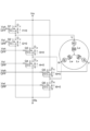
- FIG. 13 is a diagram for explaining a switch state corresponding to a free mode, which is switched by a spin control signal Id.
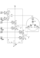
- FIG. 13 is a diagram for explaining a switch state corresponding to a charging mode, which is switched by a spin control signal Id.
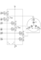
- FIG. 13 is a diagram for explaining a switch state corresponding to a discharge mode, which is switched by an idling control signal Id.
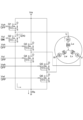
- FIG. 11 is a diagram for explaining another switch state corresponding to a charging mode, which is switched by the idling control signal Id.
- FIG. 13 is a diagram for explaining a switch state corresponding to a free mode, which is switched by a spin control signal Id.
- FIG. 13 is a diagram for explaining a switch state corresponding to a charging mode, which is switched by a spin control signal Id.
- FIG. 13 is a diagram for explaining
- FIG. 13 is a diagram for explaining a switch state in which the charging mode is not entered even when the switch is switched by the idling control signal Id.
- 2 is a diagram showing an example of the configuration of a current detection circuit 2c of the motor drive control device 10.
- FIG. 2 is a diagram showing an example of the configuration of a current measuring unit 16 included in a control circuit 1 of a motor drive control device 10.
- FIG. 1 is a diagram showing a functional block configuration of a control circuit 1 in a motor drive control device 10 according to an embodiment.
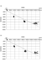
- This figure shows the relationship between the current measurement value measured by the current measuring unit 16 of the current flowing through the shunt resistor Rs due to inductive kickback when the charging time (period corresponding to the charging mode) is 10 msec and 50 msec when the rotor of the motor 3 is rotating freely in the low speed range, and the rotation speed of the motor 3.
- This figure shows the relationship between the current measurement value measured by the current measuring unit 16 of the current flowing through the shunt resistor Rs due to inductive kickback when the charging time (period corresponding to the charging mode) is 10 msec and 50 msec when the rotor of the motor 3 is rotating freely in the high speed range, and the rotation speed of the motor 3.
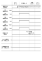
- FIG. 11 is a timing chart showing an example of a signal waveform from when a speed command signal Sc is input until a determination of idling is completed when the rotor of the motor 3 is not moving at all.
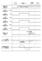
- 10 is a timing chart showing an example of a signal waveform from when a speed command signal Sc is input until a determination of idling is completed while the rotor of the motor 3 is moving.
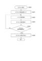
- FIG. 5 is a flowchart showing an example of a flow of processing when power is turned on in a control circuit 1 of a motor drive control device 10 according to an embodiment.
- 4 is a flowchart showing an example of the flow of an offset measurement process performed by a control circuit 1 of a motor drive control device 10.
- 4 is a flowchart showing an example of a flow of a motor idling detection process performed by a control circuit 1 of a motor drive control device 10.
- a motor drive control device (10) has a control circuit (1) that generates a drive control signal (Sd) for driving a motor having a coil of at least one phase, and an inverter circuit (2a) including high-side switches (Q1, Q3, Q5) and low-side switches (Q2, Q4, Q6) connected in series to each other and provided corresponding to the coil of each phase of the motor (3), and rotates the rotor of the motor by alternately turning on and off the high-side switch and the low-side switch in response to the drive control signal to switch the direction of current flow to the coil of the corresponding phase.
- Sd drive control signal
- inverter circuit (2a) including high-side switches (Q1, Q3, Q5) and low-side switches (Q2, Q4, Q6) connected in series to each other and provided corresponding to the coil of each phase of the motor (3), and rotates the rotor of the motor by alternately turning on and off the high-side switch and the low-side switch in response to the drive control signal to switch the direction of current flow to the coil of the
- the motor comprises a drive circuit (2) that rotates the motor, and a shunt resistor (Rs) that is provided between the inverter circuit and ground.
- the control circuit generates an idling control signal (Id) instead of the drive control signal, and switches the switch state of the inverter circuit to generate an induced current that circulates between the motor coil and the inverter circuit when the rotor of the motor is idling.
- Id idling control signal
- the control circuit may have a first switching unit (21a) that switches from a first switching state in which all of the high-side switches and the low-side switches included in the inverter circuit are turned off to a second switching state in which at least two of the high-side switches or the low-side switches included in the inverter circuit are turned on, a second switching unit (21b) that switches from the second switching state to the first switching state, and an idling determination unit (22) that determines whether the motor is idling based on the current flowing through the shunt resistor when switching from the second switching state to the first switching state.
- the second switching unit may switch the second switch state to the first switch state when a time period ten times a time constant determined by the winding resistance and inductance of the motor has elapsed.
- the second switching unit may maintain the first switch state after switching from the second switch state to the first switch state for a time until the current flowing through the shunt resistor becomes a maximum current in the inverter circuit direction from ground to the inverter circuit due to inductive kickback, or for a time of 0.5 or more times a time constant determined by the winding resistance and inductance of the motor.
- control circuit may determine that the motor is spinning when the maximum current flowing through the shunt resistor in the direction of the inverter circuit due to inductive kickback exceeds a predetermined threshold.
- the motor drive control device described in [4] above may further include a current detection circuit (2c) including the shunt resistor and a bidirectional current detection circuit capable of detecting the current flowing through the shunt resistor in both directions, that is, in the ground direction from the inverter circuit to the ground and in the inverter circuit direction, and the control circuit may further include a current measurement unit (16) that detects the signal output from the current detection circuit in advance as an offset when no current flows through the shunt resistor, and adjusts the signal output from the current detection circuit with the offset when determining whether the wheel is spinning, and outputs the signal to the wheel spin determination unit.
- a current detection circuit (2c) including the shunt resistor and a bidirectional current detection circuit capable of detecting the current flowing through the shunt resistor in both directions, that is, in the ground direction from the inverter circuit to the ground and in the inverter circuit direction
- the control circuit may further include a current measurement unit (16) that detects the signal output from the current detection circuit in advance as an
- a method for detecting idling of a motor is a method for detecting idling of a motor, which is executed in a motor drive control device having a control circuit for generating a drive control signal for driving a motor having at least one coil phase, an inverter circuit including high-side switches and low-side switches connected in series to each other and provided corresponding to the coil phases of the motor, and a drive circuit for rotating a rotor of the motor by alternately turning on and off the high-side switches and the low-side switches in response to the drive control signal to switch the direction of current flow through the coil of the corresponding phase, and a shunt resistor provided between the inverter circuit and ground, and is characterized in that it includes a first step of switching from a first switch state in which all of the high-side switches and the low-side switches included in the inverter circuit are turned off to a second switch state in which at least two of the high-side switches or the low-side switches included in the
- FIG. 1 is a diagram showing a configuration of a motor unit 100 including a motor drive control device 10 according to an embodiment.
- the motor unit 100 includes a motor 3 and a motor drive control device 10 that controls the rotation of the motor 3.
- the motor unit 100 can be applied to various devices that use a motor as a drive source, such as a fan.
- Motor 3 is, for example, a permanent magnet synchronous motor (PMSM).
- motor 3 is, for example, a surface permanent magnet synchronous motor (SPMSM) having three-phase coils (windings) Lu, Lv, and Lw.
- Coils Lu, Lv, and Lw are, for example, connected in a Y (star) configuration. In this case, the coils may also be connected in a ⁇ (delta) configuration.
- the motor drive control device 10 applies a sine wave drive signal to the motor 3, causing a periodic sine wave drive current to flow through the three-phase coils Lu, Lv, and Lw of the motor 3, thereby rotating the rotor of the motor 3.
- the motor drive control device 10 has a control circuit 1 and a drive circuit 2.
- the components of the motor drive control device 10 shown in FIG. 1 are only a part of the whole, and the motor drive control device 10 may have other components in addition to those shown in FIG. 1.
- the drive circuit 2 drives the motor 3 based on a drive control signal Sd output from the control circuit 1, which will be described later.
- the drive circuit 2 includes, for example, an inverter circuit 2a, a pre-drive circuit 2b, and a current detection circuit 2c.
- the inverter circuit 2a is disposed between the DC power supply Vin and ground potential, and drives the coils Lu, Lv, and Lw of the motor 3 as a load based on the input drive control signal Sd.
- the inverter circuit 2a has three switching legs, each including two drive transistors connected in series, and drives the motor 3 as a load by alternately turning the two drive transistors on and off (switching operation) based on the input drive control signal Sd.
- the inverter circuit 2a has switching legs corresponding to the U-phase, V-phase, and W-phase of the motor 3. As shown in FIG. 1, the switching legs corresponding to each phase have two drive transistors (hereinafter also referred to as "switching elements") Q1 and Q2, Q3 and Q4, and Q5 and Q6 connected in series between the DC power supply Vin and ground potential via a current detection circuit 2c.
- switching elements two drive transistors (hereinafter also referred to as "switching elements") Q1 and Q2, Q3 and Q4, and Q5 and Q6 connected in series between the DC power supply Vin and ground potential via a current detection circuit 2c.
- the driving transistors Q1, Q3, and Q5 (corresponding to high-side switches) on the upper arm of the coil of the motor 3 are, for example, N-channel MOSFETs
- the driving transistors Q2, Q4, and Q6 (corresponding to low-side switches) on the lower arm of the coil of the motor 3 are, for example, N-channel MOSFETs.
- the driving transistors Q1 to Q6 may be other types of FETs, for example, IGBTs (Insulated Gate MOSFETs). However, other types of transistors such as a bipolar transistor may also be used.
- the switching leg corresponding to the U phase has switching elements Q1 and Q2 connected in series.
- the common connection point of switching elements Q1 and Q2 is connected to one end of coil Lu as a load.
- the switching leg corresponding to the V phase has switching elements Q3 and Q4 connected in series.
- the common connection point of switching elements Q3 and Q4 is connected to one end of coil Lv as a load.
- the switching leg corresponding to the W phase has switching elements Q5 and Q6 connected in series.
- the common connection point of switching elements Q5 and Q6 is connected to one end of coil Lw as a load.
- switching elements Q1 and Q2, Q3 and Q4, and Q5 and Q6 each have parasitic diode characteristics from the ground side to the power supply side (not shown in FIG. 1).
- the pre-drive circuit 2b generates a drive signal for driving the inverter circuit 2a based on the drive control signal Sd output from the control circuit 1.
- the drive control signal Sd is a signal for controlling the drive of the motor 3, and is, for example, a PWM (Pulse Width Modulation) signal.
- the drive control signal Sd is a signal for switching the current pattern of the coils Lu, Lv, and Lw of the motor 3, which is determined by the on/off state of each switching element that constitutes the inverter circuit 2a.
- the drive control signal Sd includes six types of PWM signals corresponding to each switching element Q1 to Q6 of the inverter circuit 2a.
- the pre-drive circuit 2b generates six types of drive signals Vuh, Vul, Vvh, Vvl, Vwh, and Vwl that can supply sufficient power to drive the control electrodes (gate electrodes) of each of the switching elements Q1 to Q6 in the inverter circuit 2a, based on six types of PWM signals as the drive control signals Sd supplied from the control circuit 1.
- These drive signals Vuh, Vul, Vvh, Vvl, Vwh, and Vwl are input to the control electrodes (gate electrodes) of the switching elements Q1 to Q6 of the inverter circuit 2a, causing each of the switching elements Q1 to Q6 to perform an on/off operation (switching operation).
- switching operation switching operation
- the switching elements Q1, Q3, and Q5 of the upper arm and the switching elements Q2, Q4, and Q6 of the lower arm of the switching leg corresponding to each phase alternately perform an on/off operation.
- power is supplied from the DC power source Vin to each phase of the motor 3, causing the motor 3 to rotate.
- the current detection circuit 2c is connected to the DC line of the inverter circuit 2a and detects the current flowing through the DC line. Specifically, it includes one resistor (hereinafter also referred to as a "shunt resistor") Rs as a current detection element.
- the shunt resistor Rs is connected in series with the inverter circuit 2a, for example, between the DC power supply Vin and the ground potential. That is, the shunt resistor Rs of the current detection circuit 2c is connected to the negative side (ground side) of the inverter circuit 2a, for example, as shown in FIG. 1.
- the inverter circuit 2a In motor driving, the inverter circuit 2a is controlled, and the currents Iu, Iv, and Iw flowing through the three-phase coils Lu, Lv, and Lw of the motor 3 flow through the shunt resistor Rs of the current detection circuit 2c.
- the current detection circuit 2c detects the voltage drop due to the current flowing through the shunt resistor Rs from the differential voltage across the shunt resistor Rs, and outputs a current detection signal Vm corresponding to the current flowing through the shunt resistor Rs to the control circuit 1 as a detection result.
- the motor in addition to driving the motor 3 by the drive control signal Sd described above, the motor has a configuration for detecting idling of the motor to determine that the motor 3 is idling when the motor 3 is not being driven by the drive control signal Sd.
- the motor drive control device 10 of this embodiment by switching the switch state of each of the switching elements Q1 to Q6 of the inverter circuit 2a, when the rotor of the motor 3 is rotating, a current is generated that circulates between the coil of the motor 3 and the inverter circuit 2a, and then the inductive kickback that occurs when the current path is interrupted is generated, and it is determined that the motor 3 is idling based on the current that flows through the shunt resistor.
- the drive circuit 2 receives an idling control signal Id, which is different from the drive control signal Sd for driving the motor, from the control circuit 1, which will be described later, and switches each switching element constituting the inverter circuit 2a to a switch state for detecting idling of the motor 3 based on the received idling control signal Id. Specifically, each switching element constituting the inverter circuit 2a is switched to a switch state corresponding to one of three modes (free mode, charge mode, discharge mode) based on the idling control signal Id. The three modes for detecting idling of the motor 3 will be described later.
- the idling control signal Id is a signal for switching each of the switching elements that make up the inverter circuit 2a to a switch state corresponding to three modes for detecting idling of the motor 3. Unlike the drive control signal Sd for driving the motor, the idling control signal Id is not a signal for generating a drive voltage in the coil of the motor 3, and is therefore not a signal that alternately switches each switching element on and off, but is, for example, a high or low signal with a predetermined length.
- the idling control signal Id includes six types of signals corresponding to each of the switching elements Q1 to Q6 of the inverter circuit 2a.
- the pre-drive circuit 2b generates a drive signal as a switching signal for switching the switch state of each switching element that constitutes the inverter circuit 2a based on the idling control signal Id output from the control circuit 1.
- the pre-drive circuit 2b generates signals capable of supplying sufficient power to switch the switch state of the control electrodes (gate electrodes) of each of the switching elements Q1 to Q6 of the inverter circuit 2a, based on six types of signals as the idling control signal Id supplied from the control circuit 1.
- the switch state of each of the switching elements Q1 to Q6 is switched by inputting drive signals as these switching signals to the control electrodes (gate electrodes) of each of the switching elements Q1 to Q6 of the inverter circuit 2a.
- FIGS. 2 to 6 are diagrams for explaining the switch states that are switched by the idling control signal Id.
- the arrows indicate the state of the current that flows through the coil of the motor 3 and the inverter circuit 2a when the motor 3 is idling.
- the inverter circuit 2a is connected to the DC power source Vin and is also connected to ground via a shunt resistor Rs, which is part of the current detection circuit 2c.
- the idling control signal Id is a signal that switches between the corresponding switch states in the order of free mode (Fig. 2), charge mode (Figs. 3 and 5), and discharge mode (Fig. 4). Specifically, the idling control signal Id switches the switch state of the control electrodes (gate electrodes) of each switching element Q1 to Q6 of the inverter circuit 2a from the first switch state (corresponding to free mode) shown in Fig. 2 to the second switch state (corresponding to charge mode) shown in Fig. 3, and then back to the first switch state (corresponding to discharge mode) as shown in Fig. 4, thereby making it possible to detect idling of the motor 3.
- the second switch state is a switch state in which, when the rotor of the motor 3 is idling, an induced voltage is generated in the coils of each phase, and the generated current circulates in a closed circuit formed by the coils and the switching elements among the switching elements Q1 to Q6 that are turned on.
- the first switch state in which all the switching elements Q1 to Q6 are turned off is switched to a second switch state in which only the switching elements Q2, Q4, and Q6 of the lower arms of the switching elements Q1 to Q6 are turned on, as shown in FIG. 3.
- the rotation of the rotor relative to the coil generates in each phase coil an induced voltage (eu, ev, ew) proportional to the rotation speed, with a polarity in the direction that generates a current that impedes changes in the magnetic flux, with the rotor rotating relative to the coil, with the rotor rotating at an electrical angle period of the motor rotation with each phase shifted by 120 degrees.
- the current waveform is 90 degrees out of phase with the voltage waveform.
- the control electrodes (gate electrodes) of the switching elements Q1 to Q6 of the inverter circuit 2a are switched from the second switch state back to the first switch state by the idling control signal Id output from the control circuit 1.
- the switch states of the switching elements Q2, Q4, and Q6 of the lower arms of the switching elements Q1 to Q6 are switched on, and then switched back to the first switch state in which all of the switching elements Q1 to Q6 are switched off, as shown in FIG.
- the current detection circuit 2c detects the current flowing through the shunt resistor Rs due to the inductive kickback that occurs in the discharge mode, and if it is determined that a predetermined current is flowing, it can determine that the motor 3 is idling.
- the second switch state corresponding to the charging mode is described by taking as an example a case where the switch states of the lower arm switching elements Q2, Q4, and Q6 of the switching elements Q1 to Q6 of the inverter circuit 2a are turned on as shown in FIG. 3, but this is not limiting.
- the second switch state includes, as shown in FIG. 5, a switch state in which any two of the switching elements Q1, Q3, and Q5 of the upper arm of each switching element Q1 to Q6 or the switching elements Q2, Q4, and Q6 of the lower arm (Q2 and Q4 in FIG. 5) are turned on.
- a switch state in which any two of the switching elements Q1, Q3, and Q5 of the upper arm of each switching element Q1 to Q6 or the switching elements Q2, Q4, and Q6 of the lower arm (Q2 and Q4 in FIG. 5) are turned on.
- the second switch state can be said to be a switch state in which, when the rotor of the motor 3 is rotating freely, an induced voltage is generated in the coil of each phase, and an induced current generated in a closed circuit formed by the coil and a transistor among the switching elements Q1 to Q6 that is turned on always circulates.
- the current detection circuit 2c is a circuit for detecting the current flowing through the three-phase coils Lu, Lv, and Lw of the motor 3 when the inverter circuit 2a is controlled during motor drive, and for detecting idling of the motor when an induced current is generated that circulates between the coils Lu, Lv, and Lw of the motor 3 and the inverter circuit 2a, and then detecting the current flowing through the shunt resistor Rs due to inductive kickback that occurs when the path of the induced current is interrupted.
- the current detection circuit 2c outputs a current detection signal Vm corresponding to the current flowing through the shunt resistor Rs to the control circuit 1.
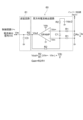
- FIG. 7 is a diagram showing an example of the configuration of the current detection circuit 2c of the motor drive control device 10.
- the current detection circuit 2c includes a bidirectional current detection circuit 60 and a delay circuit 61.
- the current detection circuit 2c in FIG. 7 outputs a current detection signal Vm that corresponds to the current flowing through the shunt resistor Rs.
- the bidirectional current detection circuit 60 in FIG. 7 acquires the differential voltage across the shunt resistor Rs, amplifies it with a predetermined gain using an amplifier section that uses a differential amplifier circuit, and outputs it as a voltage drop signal Vout across the shunt resistor Rs.
- the delay circuit 61 smoothes the voltage drop signal Vout using a circuit consisting of resistor R3 and capacitor C3, and outputs it to the control circuit 1 as a current detection signal Vm corresponding to the current flowing through the shunt resistor Rs.
- the bidirectional current detection circuit 60 is configured to apply a voltage that offsets the amplifier output to the positive terminal of the OPAMP, making it possible to detect both positive and negative voltage drops that occur across the shunt resistor Rs, that is, to measure bidirectional currents.
- the voltage that offsets the amplifier output is not limited to Vdc/2, and a voltage that offsets the amplifier output may be applied to the negative terminal of the OPAMP.
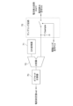
- FIG. 8 is a diagram showing an example of the configuration of the current measurement unit 16 included in the control circuit 1 of the motor drive control device 10.
- the current measurement unit 16 has a sampling circuit 70, a D/A converter 71, a comparator 72, and an offset calculator 73.
- the current measurement unit 16 in FIG. 8 performs A/D conversion at a predetermined timing on the current detection signal Vm, which corresponds to the current flowing through the shunt resistor Rs input from the current detection circuit 2c, and further performs offset adjustment, which will be described later, to generate a current measurement value Ival used by the control circuit 1.
- the current measurement value Ival is a value that corresponds to the current flowing through the shunt resistor Rs of the current detection circuit 2c.
- the sampling circuit 70 in FIG. 8 is composed of, for example, a switch and a capacitor, and the switch is switched on and off in response to drive trigger signals Tr and Ir output from the timing adjustment unit 15 or state control unit 12 of the control circuit 1 described later, thereby performing A/D conversion on the current detection signal Vm, which is the output voltage of the current detection circuit 2c, at a predetermined timing.
- the A/D conversion is performed by sampling by the sampling circuit 70 and quantization by a D/A converter 71 and a comparator 72.
- the value generated by the A/D conversion is further subjected to offset adjustment by an offset calculator 73 described later, and a current measurement value Ival corresponding to the current flowing through the shunt resistor Rs is generated.
- the current measurement value Ival is used by the vector control unit 13 as the current measurement values Iu, Iv, and Iw in motor drive.
- the current measurement value Ival is also used by the idling determination unit 22 of the state control unit 12 described later in the control circuit 1 to detect idling of the motor.
- the control circuit 1 In driving the motor, the control circuit 1 generates a drive control signal Sd for driving the motor 3 based on a speed command signal Sc that is input from outside and indicates a target state for the operation of the motor 3, and controls the driving of the motor 3. Specifically, the control circuit 1 generates a drive control signal Sd so that the motor 3 is in the operating state specified by the speed command signal Sc, and provides it to the drive circuit 2.
- the control circuit 1 also generates an idling control signal Id instead of the drive control signal Sd when detecting idling of the motor 3, and detects idling of the motor 3. Specifically, the control circuit 1 generates an idling control signal Id so that each of the switching elements Q1 to Q6 of the inverter circuit 2a is in the switch state specified by the idling control signal Id, and provides it to the drive circuit 2.
- the state control unit 12 which will be described later, further generates an idling trigger signal Ir when detecting idling of the motor, and generates a current measurement value Ival from the current detection signal Vm detected in the current detection circuit 2c. Specifically, the state control unit 12 generates an idling trigger signal Ir that switches on the sampling circuit 70 at a predetermined timing, and provides it to the current measurement unit 16. Although not specifically shown in FIG. 9, the state control unit 12 may further have a functional unit that executes such processing.
- control circuit 1 is a program processing device (e.g., a microcontroller) having a configuration in which a processor such as a CPU, various storage devices such as RAM and ROM, and peripheral circuits such as a counter (timer), an A/D conversion circuit, a D/A conversion circuit, a clock generation circuit, and an input/output I/F circuit are connected to each other via a bus or dedicated lines.
- a processor such as a CPU
- various storage devices such as RAM and ROM
- peripheral circuits such as a counter (timer), an A/D conversion circuit, a D/A conversion circuit, a clock generation circuit, and an input/output I/F circuit are connected to each other via a bus or dedicated lines.
- the motor drive control device 10 may be configured such that at least a portion of the control circuit 1 and at least a portion of the drive circuit 2 are packaged as a single integrated circuit device (IC), or the control circuit 1 and the drive circuit 2 are each packaged as separate integrated circuit devices.
- IC integrated circuit device
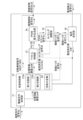
- FIG. 9 is a diagram showing the functional block configuration of the control circuit 1 in the motor drive control device 10 according to the embodiment.
- the control circuit 1 has, for example, a drive command acquisition unit 11, a state control unit 12, a vector control unit 13, a PWM signal generation unit 14, a timing adjustment unit 15, and a current measurement unit 16 as functional blocks for generating a drive control signal Sd when driving a motor by vector control.
- the control circuit 1 also has a state control unit 12 and a current measurement unit 16 as functional blocks for generating a spin control signal Id when detecting spinning of the motor.
- the state control unit 12 has a first switching unit 21a, a second switching unit 21b, and a spin determination unit 22.
- These functional blocks are realized, for example, by a processor in a program processing device serving as the control circuit 1, which executes various arithmetic operations according to programs stored in memory and controls peripheral circuits such as counters and A/D conversion circuits.
- the drive command acquisition unit 11 receives a speed command signal Sc from the outside and analyzes the received speed command signal Sc to acquire a value that specifies the target operating state of the motor 3 specified by the speed command signal Sc.
- the speed command signal Sc includes a value indicating the target state of operation of the motor 3.
- the speed command signal Sc is, for example, a signal output from a higher-level device for controlling the motor unit 100, which is provided outside the motor drive control device 10.
- the speed command signal Sc specifies, for example, the rotation speed of the rotor of the motor 3.
- the speed command signal Sc includes a value ⁇ ref of the target rotation speed (target rotation speed) of the rotor of the motor 3.
- the speed command signal Sc is, for example, a PWM signal having a duty ratio corresponding to the specified target rotation speed ⁇ ref.
- the drive command acquisition unit 11 measures, for example, the duty ratio of the PWM signal of the speed command signal Sc, and outputs the rotation speed corresponding to the measured duty ratio as the target rotation speed ⁇ ref.
- the state control unit 12 When driving the motor, the state control unit 12 outputs the target rotation speed ⁇ ref as is to the vector control unit 13. When a slip determination signal, which will be described later, is generated from the slip determination unit 22, the state control unit 12 can determine the motor starting method. Although not specifically shown in FIG. 9, the state control unit 12 may further have a functional unit that executes such processing.
- the vector control unit 13 generates voltage values V ⁇ and V ⁇ from the target rotation speed ⁇ ref and the current measurement value Ival according to well-known vector control, and outputs them to the PWM signal generation unit 14 (space vector modulation circuit: SVM (Space Vector Modulation) circuit).
- SVM Space Vector Modulation
- the PWM signal generating unit 14 outputs a drive control signal Sd to the drive circuit 2 to PWM control the drive circuit 2, and outputs a PWM count signal Tc, which is a signal indicating the start of PWM counting in the PWM control, to the timing adjustment unit 15.
- the timing adjustment unit 15 starts the counter for generating timing in synchronization with the start of the PWM count, and triggers the current measurement unit 16. Specifically, the timing adjustment unit 15 outputs a drive trigger signal Tr to the current measurement unit 16 at the current capture timing based on the PWM count signal Tc output from the PWM signal generation unit 14.
- the current measurement unit 16 performs A/D conversion on the current detection signal Vm corresponding to the currents Iu, Iv, and Iw based on the drive trigger signal Tr, and then performs offset adjustment (described later) to generate the current measurement value Ival.
- the current measurement value Ival is output to the vector control unit 13, which performs vector control from the three-phase current values based on the timing signal St from the timing adjustment unit 15, and calculates the magnitude of current flow in the PWM signal generation unit 14.
- the state control unit 12 When detecting idling of the motor, the state control unit 12 outputs an idling trigger signal Ir to the current measurement unit 16 at a predetermined timing to switch on the sampling circuit 70, instructing the current measurement unit 16 to measure the current detection signal Vm, and also performs A/D conversion on the input current detection signal Vm, and further performs offset adjustment (described later) to generate the current measurement value Ival.
- the current detection circuit 2c is capable of measuring the current flowing in both directions through the shunt resistor Rs when driving the motor and detecting idling of the motor. Therefore, in the bidirectional current detection circuit 60 of the current detection circuit 2c, the voltage drop signal Vout in the shunt resistor Rs and the current detection signal Vm are offset by Vdc/2. For this reason, the current measurement unit 16 has a current measurement value Ival other than zero when no current flows through the shunt resistor Rs.
- the state control unit 12 performs A/D conversion on the current detection signal Vm input to the current measurement unit 16 when in free mode or charging mode, which is a state in which no current flows through the shunt resistor Rs, and obtains an offset value in advance. This obtained offset value is used by the offset calculator 73 of the current measurement unit 16.
- the state control unit 12 outputs an idling trigger signal Ir that switches on the sampling circuit 70 of the current measurement unit 16, performs A/D conversion on the current detection signal Vm input from the current detection circuit 2c, and specifies the current measurement value generated by disabling the offset calculator 73 as the offset value.
- the offset calculator 73 may be disabled and the current measurement value generated multiple times may be repeated, and the average value of the current measurement values generated multiple times may be set as the offset value.
- the current detection signal Vm detected at this time can be used as a reference for zero current and can be used as an offset to be used when generating the current measurement value Ival.
- This offset adjustment may be performed in the free mode immediately after power is turned on or immediately after the speed command signal Sc is input, or may be performed in the charge mode after the speed command signal Sc is input.
- the state control unit 12 When the state control unit 12 is in discharge mode during motor idling detection, i.e. when the switch state is switched from the second switch state to the first switch state, it outputs an idling trigger signal Ir to the current measurement unit 16 at a predetermined timing to switch on the sampling circuit 70, instructing the current measurement unit 16 to measure the input current detection signal Vm, and also performs A/D conversion on the input current detection signal Vm and performs offset adjustment to generate the current measurement value Ival.
- the current measurement unit 16 outputs the generated current measurement value Ival to the idling determination unit 22 of the state control unit 12.
- the idling determination unit 22 determines whether the motor 3 is idling based on the measured current value Ival generated by the current measurement unit 16, and generates an idling determination signal indicating the idling determination result. Specifically, the idling determination unit 22 compares a preset idling threshold value with the measured current value Ival generated by the current measurement unit 16, and determines that the motor 3 is idling when the maximum measured current value Ival on the negative side, which is the inverter circuit direction, exceeds the threshold value and is smaller than the idling threshold value (the negative value is large).
- inductive kickback occurs when the motor switches to discharge mode, and a current flows from the ground side to the inverter circuit 2a side.
- the motor 3 is idling at high speed, the induced voltage and induced current increase, so the period of inductive kickback becomes longer and the current flowing through the shunt resistor Rs in the direction of the inverter circuit becomes larger, and this is used for the judgment.
- the idling judgment unit 22 can adopt, for example, as the idling threshold value, a value in the range from the current measurement value (small negative value) due to the current flowing through the shunt resistor Rs due to inductive kickback when the motor 3 is stopped to the current measurement value (large negative value) corresponding to the current flowing through the shunt resistor Rs due to inductive kickback when the motor 3 is idling at the lowest rotation speed.
- the idling threshold value a value in the range from the current measurement value (small negative value) due to the current flowing through the shunt resistor Rs due to inductive kickback when the motor 3 is stopped to the current measurement value (large negative value) corresponding to the current flowing through the shunt resistor Rs due to inductive kickback when the motor 3 is idling at the lowest rotation speed.
- the first switching unit 21a In the state control unit 12, the first switching unit 21a generates a first idling control signal Id1 that switches the switching elements Q1 to Q6 that make up the inverter circuit 2a to a first switch state.
- the second switching unit 21b In the state control unit 12, the second switching unit 21b generates a second idling control signal Id2 that switches the switching elements Q1 to Q6 that make up the inverter circuit 2a to a second switch state.
- the first and second idling control signals Id generated by the first switching unit 21a and the second switching unit 21b of the state control unit 12 are output to the drive circuit 2.
- the first switching unit 21a In the state control unit 12, in order to set the switch state to enable spin detection, after power is turned on, the first switching unit 21a generates the first spin control signal Id1 corresponding to the free mode until the drive command acquisition unit 11 receives the speed command signal Sc. In the state control unit 12, the second switching unit 21b generates the second spin control signal Id2 during the charging time (period corresponding to the charging mode). In the state control unit 12, the first switching unit 21a again generates the first spin control signal Id1 during the discharging time (period corresponding to the discharging mode). Note that after the discharging time, the first switching unit 21a may generate the first spin control signal Id1 corresponding to the free mode.
- the timing for transitioning from the free mode to the charging mode may be, for example, after the drive command acquisition unit 11 receives the speed command signal Sc.
- the charging time can be set to 10 times the time constant determined by the winding resistance and inductance of the coil of motor 3.
- the coil of motor 3 can be considered as an RL series circuit because it has winding resistance and inductance, and the time until the winding current stabilizes is 10 times the time constant.
- the time constant is 1 msec.
- the charging time can be set to 10 msec. A longer charging time makes it clearer to distinguish between motor stoppage and idling at low rotation speeds, but a shorter charging time is preferable because it shortens the inspection period for idling detection.
- the discharge time is sufficient if it is equal to or greater than the time constant of the delay circuit 61 in the current detection circuit 2c, because the current flowing through the shunt resistor Rs in the inverter circuit direction converges to zero due to attenuation caused by inductive kickback. If the maximum current can be measured in the inverter circuit direction, it can be determined whether the motor is in an idling state, and it can be determined that the discharge time has been reached.
- the discharge time can also be set to 0.5 times the time constant determined by the winding resistance and inductance of the coil of the motor 3.
- the time constant of 0.5 times is the timing at which the current flowing through the shunt resistor Rs in the inverter circuit direction converges to about 60% of the peak value due to attenuation, but in the discharge mode, it is sufficient if the maximum current in the inverter direction at the shunt resistor Rs can be detected.
- the time constant is 1 msec. In this case, the discharge time can be set to 0.5 msec.
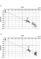
- Figures 10 and 11 are diagrams showing the relationship between the current measurement value generated by the current measurement unit 16 for the current flowing through the shunt resistor due to inductive kickback and the rotation speed of the motor 3.
- the charging time (period corresponding to the charging mode) is 50 msec
- the charging time (period corresponding to the charging mode) is 10 msec.
- FIG. 10 shows a case where the rotor of motor 3 is rotating freely in the low-speed range during the charging time (the period corresponding to the charging mode)
- FIG. 11 shows a case where the rotor of motor 3 is rotating freely in the high-speed range.
- the vertical axis shows the current measurement value generated by current measuring unit 16 for the current flowing through the shunt resistor due to inductive kickback
- the horizontal axis shows the rotation speed (rpm) of motor 3. At this time, the current measurement value has been offset adjusted.
- FIG. 10 and 11 show the current measurement values generated by the current measuring unit 16 for the current flowing through the shunt resistor due to inductive kickback observed at each rotation speed of the motor 3.
- the current measurement value is a negative (-) value because the current flows from the ground side to the inverter circuit 2a side in the shunt resistor Rs.
- the current measurement value and the motor rotation speed are in a roughly proportional relationship over a wide range of rotation speeds of the motor 3. It can be said that the rotation is essentially stopped at 250 rpm or less.
- the current measurement value is less than -400 whether the charging time is 10 msec or 50 msec. Therefore, it can be seen that the current flowing through the shunt resistor due to inductive kickback does not depend on the charging time, and if the charging time is 10 msec, it is sufficiently possible to detect the rotation.
- Figures 12 and 13 are timing charts showing an example of a signal waveform from when the speed command signal Sc is input after power is applied to the motor unit 100 until the determination of freewheeling is completed.
- Figure 12 is a timing chart when the rotor of the motor 3 is not moving at all
- Figure 13 is a timing chart when the rotor of the motor 3 is moving (freewheeling).
- the shunt current Is is the current that flows through the shunt resistor Rs of the current detection circuit 2c, and is a current that corresponds to the current detection signal Vm.
- the motor drive control device 10 is shown passing through free mode, charge mode, and discharge mode, and then returning to free mode again. At this time, the motor drive control device 10 starts in free mode after power is turned on. Note that the timing charts shown in Figures 12 and 13 give an example of a case where the free mode is entered again after discharge mode, but this is not limited to this.
- the idling control signal Id1 sets the inverter circuit 2a to a first switch state. Specifically, the idling control signal Id1 sets all of the drive signals input to the gates of the switching elements Q1 to Q6 that make up the inverter circuit 2a low, turning off all of the switches in the inverter circuit. In this state, regardless of whether the motor is idling or not, no closed circuit is formed between the coil of the motor 3 and the inverter circuit 2a, so the current in the coil of the motor 3 becomes zero. In addition, no current flows through the shunt resistor Rs.
- the idling trigger signal Ir for measuring the shunt current Is is low.
- the idling trigger signal Ir may be set to high at a predetermined timing.
- the current measuring unit 16 acquires the current detection signal Vm output from the current detection circuit 2c, and can use it as an offset since no current flows through the shunt resistor Rs.
- the idling control signal Id2 sets the inverter circuit 2a to the second switch state. Specifically, the idling control signal Id2 sets all of the drive signals input to the gates of the lower arm switching elements Q2, Q4, and Q6 of the switching elements Q1 to Q6 that make up the inverter circuit 2a to high, turning off all of the low-side switches of the inverter circuit.
- the idling trigger signal Ir for measuring the shunt current Is is low. However, during this period, it may be made high at a specified timing. In this case, the current measuring unit 16 acquires the current detection signal Vm output from the current detection circuit 2c, and since no current flows through the shunt resistor Rs, it can be used as an offset. Note that if an offset is acquired in the free mode, it is not necessary to acquire the offset again at this timing.
- the idling control signal Id1 causes the inverter circuit 2a to be again in the first switch state. Specifically, the idling control signal Id1 causes all of the drive signals input to the gates of the switching elements Q1 to Q6 that make up the inverter circuit 2a to be again low, turning off all of the switches in the inverter circuit.
- the idling trigger signal Ir for measuring the shunt current Is goes high at a predetermined timing.
- the predetermined mask time is set as a period for removing switching noise of the inverter circuit 2a caused by the drive signal being turned off.
- the current measurement unit 16 acquires the current detection signal Vm output from the current detection circuit 2c and measures the current flowing through the shunt resistor Rs.
- Figure 13 shows the shunt current Is and the U-phase winding current in two states.
- the amplitude of the U-phase winding current (dotted line) is small in charge mode, and a small shunt current (dotted line) is generated on the negative side, which is the direction of the inverter circuit, due to inductive kickback in discharge mode, and the current flowing in the inverter circuit direction of shunt resistor Rs is small.
- FIG. 14 is a flowchart showing an example of the flow of processing when power is turned on in the control circuit 1 of the motor drive control device 10 according to the embodiment.
- FIG. 15 is a flowchart showing an example of the flow of offset measurement processing by the control circuit 1 of the motor drive control device 10.
- FIG. 16 is a flowchart showing an example of the flow of idling detection processing by the control circuit 1 of the motor drive control device 10.
- the first switching unit 21a When the motor drive control device 10 is powered on, as shown in FIG. 14, in the state control unit 12, the first switching unit 21a generates a first idling control signal Id1 that switches the switching elements Q1 to Q6 that make up the inverter circuit 2a to a first switch state corresponding to the free mode (step S101).
- the state control unit 12 generates an idling control signal Id1 that switches the switching elements Q1 to Q6 that make up the inverter circuit 2a to the first switch state in accordance with the first idling control signal Id1 generated in step S101.
- the switching elements Q1 to Q6 that make up the inverter circuit 2a are set to the first switch state as shown in FIG. 2.
- step S200 the state control unit 12 executes the offset measurement process.
- step S201 When the state control unit 12 starts the offset measurement process, as shown in FIG. 15, it first clears the counter for the number of offset measurements and disables the offset calculator 73 (step S201).
- the state control unit 12 outputs an idling trigger signal Ir, switches the sampling circuit 70 of the current measurement unit 16, performs A/D conversion on the current detection signal Vm output from the current detection circuit 2c, and generates a current measurement value Ival corresponding to the current flowing through the shunt resistor Rs (step S202). Note that although the shunt current Is at this time is zero, the voltage that offsets the amplifier of the bidirectional current detection circuit 60 causes the current measurement value Ival to become a value other than zero.
- step S203 the state control unit 12 increments the counter for the number of offset measurements by "+1" (step S203).
- the state control unit 12 checks the counter for the number of offset measurements and determines whether the current number of offset measurements exceeds a predetermined number of offset measurements (step S204).
- step S204 If the current number of offset measurements does not exceed the predetermined number of offset measurements (step S204: No), the process returns to step S202. On the other hand, if the current number of offset measurements exceeds the predetermined number of offset measurements (step S204: Yes), the average value of the values obtained in the measurements in step S202 is obtained as the offset value, and the offset calculator 73 is enabled (step S205).
- the state control unit 12 determines whether the drive command acquisition unit 11 has received a speed command signal Sc from a higher-level device (step S102).
- step S102 If it is determined that the speed command signal Sc has not been received (step S102: No), step S102 is repeated after a predetermined time.
- step S300 If it is determined that the speed command signal Sc has been received (step S102: Yes), the slip detection process is executed (step S300).
- the second switching unit 21b in the state control unit 12 first generates a second spin control signal Id2 that switches to the second switch state corresponding to the charge mode, as shown in FIG. 16 (step S301). At this time, the charge time is reset in the state control unit 12.
- the state control unit 12 generates an idling control signal Id2 that switches the switching elements Q1 to Q6 that make up the inverter circuit 2a to the second switch state in accordance with the second idling control signal Id2 generated in step S301.
- the switching elements Q1 to Q6 that make up the inverter circuit 2a are switched to the second switch state, for example as shown in FIG. 3.
- the second switching unit 21b determines whether a predetermined charging time has elapsed since the second idling control signal Id2 was generated in step S301 (step S302).
- step S302 When a predetermined charging time has elapsed since the second switching unit 21b in the state control unit 12 generated the second idling control signal Id2 (step S302: Yes), the first switching unit 21a in the state control unit 12 generates a first idling control signal Id1 that switches to the first switch state corresponding to the discharge mode (step S303). At this time, the discharge time and mask time are reset in the state control unit 12.
- the state control unit 12 switches the switching elements Q1 to Q6 that constitute the inverter circuit 2a to the first switch state by generating the first idling control signal Id1 generated in step S303. That is, in response to this idling control signal Id1, the switching elements Q1 to Q6 that constitute the inverter circuit 2a are again in the first switch state, for example as shown in FIG. 4.
- the state control unit 12 determines whether the mask time has elapsed (step S304). If the mask time has elapsed (step S304: Yes), the state control unit 12 executes the shunt current measurement process (step S305).
- the state control unit 12 outputs an idling trigger signal Ir to the current measurement unit 16, switches the sampling circuit 70 of the current measurement unit 16, performs A/D conversion on the current detection signal Vm output from the current detection circuit 2c, and further performs offset adjustment to generate the current measurement value Ival.
- the current measurement unit 16 outputs the current measurement value Ival to the idling determination unit 22 of the state control unit 12.
- the current measurement value Ival corresponds to the current flowing through the shunt resistor Rs of the current detection circuit 2c.
- the state control unit 12 determines whether the discharge time has elapsed (step S306). When the discharge time has elapsed (step S306: Yes), the state control unit 12 ends the shunt current measurement process and enters free mode (step S307). On the other hand, when the discharge time has not elapsed (step S306: No), the state control unit 12 executes the shunt current measurement process again (step S305).
- the idling determination unit 22 determines whether the motor 3 is idling based on the maximum current measurement value in the inverter circuit direction generated by the current measurement unit 16 (step S308). In step S308, the idling determination unit 22 compares the maximum current measurement value in the inverter circuit direction with the idling threshold value to determine whether the motor 3 is idling.
- the idling determination unit 22 may convert the current measurement value Ival generated for the current detection signal Vm received from the current measurement unit 16 to an actual current value and then compare it with the threshold current value, or may compare the current measurement value Ival generated without offset adjustment for the current detection signal Vm received from the current measurement unit 16 with the threshold value without offset adjustment.
- the idling determination unit 22 determines that the motor 3 is idling when the maximum current measurement value on the negative side, which is the inverter circuit direction, exceeds the threshold value and is smaller than the idling threshold value (the negative value is large) (Step S308: Yes).
- step S308: No the idling determination unit 22 determines that the motor 3 is stopped (not idling).
- the idling determination unit 22 generates a idling determination signal that indicates the idling determination result.
- the idling determination signal is used by the state control unit 12.
- the state control unit 12 determines whether the motor 3 is in a free-spin state from the generated spin determination signal (step S103), and if it is determined that the motor 3 is in a free-spin state (step S103: Yes), it outputs the target rotation speed ⁇ ref to the vector control unit 13 and drives the motor by vector control. On the other hand, if the state control unit 12 determines that the motor 3 is not in a free-spin state (step S103: No), it drives the motor by braking, excitation, forced commutation start, etc.
- the control circuit 1 of the motor drive control device 10 switches the switch state of each of the switching elements Q1 to Q6 of the inverter circuit 2a to generate an induced current circulating between the coil of the motor 3 and the inverter circuit 2a when the rotor of the motor 3 is spinning freely.
- the control circuit 1 determines that the motor 3 is spinning freely based on the current flowing through the shunt resistor Rs due to the inductive kickback that occurs in the inverter circuit.
- the motor drive control device 10 can accurately detect whether the motor 3 is in an idling state in a short time without using a position sensor or a measurement circuit for each phase voltage.
- the control circuit 1 has a first switching unit 21a that switches from a first switching state in which all of the high-side switches and the low-side switches included in the inverter circuit are turned off to a second switching state in which at least two of the high-side switches or the low-side switches included in the inverter circuit are turned on, a second switching unit 21b that switches from the second switching state to the first switching state, and an idling determination unit 22 that determines whether the motor is idling based on the current flowing through the shunt resistor when switching from the second switching state to the first switching state.
- the second switching unit switches the second switch state to the first switch state when a time period that is 10 times the time constant determined by the winding resistance and inductance of the motor has elapsed.
- the first switching unit after switching from the second switch state to the first switch state, the first switching unit maintains the first switch state until the current flowing through the shunt resistor becomes a maximum current in the inverter circuit direction from ground to the inverter circuit due to inductive kickback, or for a time that is 0.5 times or more of the time constant determined by the winding resistance and inductance of the motor.
- control circuit determines that the motor is spinning when the maximum current flowing through the shunt resistor in the inverter circuit direction due to inductive kickback exceeds a predetermined threshold value.
- the motor drive control device 10 further includes a current detection circuit 2c including the shunt resistor and a bidirectional current detection circuit capable of detecting the current flowing through the shunt resistor in both directions, that is, in the ground direction from the inverter circuit to the ground and in the inverter circuit direction, and the control circuit further includes a current measurement unit 16 that detects the signal output from the current detection circuit as an offset in advance when no current flows through the shunt resistor, and adjusts the signal output from the current detection circuit with the offset when determining whether the wheel is spinning, and outputs the signal to the wheel spin determination unit.
- a current detection circuit 2c including the shunt resistor and a bidirectional current detection circuit capable of detecting the current flowing through the shunt resistor in both directions, that is, in the ground direction from the inverter circuit to the ground and in the inverter circuit direction
- the control circuit further includes a current measurement unit 16 that detects the signal output from the current detection circuit as an offset in advance when no current flows through the shunt resistor
- the speed command signal Sc includes a target value (target rotation speed) of the rotation speed of the motor 3, but this is not limited to the above.
- the speed command signal Sc may be a torque command signal that specifies the torque of the motor 3.
- the motor drive control device 10 is described based on an example in which a position sensor or a measurement circuit for each phase voltage is not used, but a position sensor or a measurement circuit for each phase voltage may be provided. Even in this case, it is not necessary to use a position sensor or a measurement circuit for each phase voltage when detecting idling.
- a Hall element that outputs a Hall signal may be used as the position sensor, or instead of such a Hall signal, another signal corresponding to the rotational position of the rotor of the motor 3 may be configured to be input as the rotational position detection signal.
- an encoder or resolver may be provided, and the detection signal may be input to the control circuit 1.
- the measurement circuit for each phase voltage may be configured to input the signal of an A/D converter or a comparator that compares each phase voltage with the neutral point voltage as the rotational position detection signal.
- control circuit 1 is not limited to the above-mentioned circuit configuration, and various circuit configurations that are configured to meet the object of the present invention can be applied to the control circuit 1.
- a spin determination circuit instead of the sampling circuit 70, a spin determination circuit may be configured using a comparator, and a signal serving as a spin threshold may be output from the D/A converter. When the maximum current detection signal Vm in the inverter circuit direction exceeds this spin threshold, it may be determined that the motor is spinning, and a spin determination signal may be output to the state control unit 12.
- the motor may be put into a short brake state in the charging mode, while the motor is judged to be running idly in the discharging mode and the motor may be kept waiting to be stopped.
- the motor drive is not limited to sine wave drive.
- the number of phases of the motor 3 driven by the motor drive control device 10 is not limited to three phases.
Landscapes
- Engineering & Computer Science (AREA)
- Power Engineering (AREA)
- Control Of Ac Motors In General (AREA)
- Control Of Motors That Do Not Use Commutators (AREA)
Abstract
Description
先ず、本願において開示される発明の代表的な実施の形態について概要を説明する。なお、以下の説明では、一例として、発明の構成要素に対応する図面上の参照符号を、括弧を付して記載している。
以下、本発明の実施の形態の具体例について図を参照して説明する。なお、以下の説明において、各実施の形態において共通する構成要素には同一の参照符号を付し、繰り返しの説明を省略する。
図1は、実施の形態に係るモータ駆動制御装置10を備えたモータユニット100の構成を示す図である。
Bipolar Transistor)等の他の種類のトランジスタであってもよい。
電源投入後、速度指令信号Scにより、制御回路1から、空転制御信号Idが出力されると、制御回路1から出力される空転制御信号Idによって、インバータ回路2aの各スイッチング素子Q1~Q6の制御電極(ゲート電極)が第1のスイッチ状態に切り替えられる。具体的には、図2に示すように、インバータ回路2aにおいて、各スイッチング素子Q1~Q6の全てのスイッチ状態がオフに切り替えられる。
次に、制御回路1から出力される空転制御信号Idによって、インバータ回路2aの各スイッチング素子Q1~Q6の制御電極(ゲート電極)が第1のスイッチ状態から第2のスイッチ状態に切り替えられる。第2のスイッチ状態は、モータ3のロータが空転していると、各相のコイルに誘起電圧が発生し、コイルと、スイッチング素子Q1~Q6のうちのオンにされたスイッチング素子とにより形成される閉回路において、発生した電流が循環するようなスイッチ状態である。具体的には、インバータ回路2aにおいて、各スイッチング素子Q1~Q6の全てのスイッチ状態をオフとする第1のスイッチ状態から、例えば、図3に示すように、各スイッチング素子Q1~Q6の下側アームのスイッチング素子Q2,Q4,Q6のみのスイッチ状態をオンとする第2のスイッチ状態に切り替えられる。
次に、制御回路1から出力される空転制御信号Idによって、インバータ回路2aの各スイッチング素子Q1~Q6の制御電極(ゲート電極)が第2のスイッチ状態から再び第1のスイッチ状態に切り替えられる。具体的には、例えば、インバータ回路2aにおいて、各スイッチング素子Q1~Q6の下側アームのスイッチング素子Q2,Q4,Q6のスイッチ状態をオンとする第2のスイッチ状態から、図4に示すように、各スイッチング素子Q1~Q6の全てのスイッチ状態をオフとする第1のスイッチ状態に再び切り替えられる。
このオフセット調整は、電源投入直後、または速度指令信号Scが入力された直後のフリーモードに行われてもよいし、速度指令信号Scが入力された後の充電モードに行われてもよい。
以上、本発明者によってなされた発明を実施の形態に基づいて具体的に説明したが、本発明はそれに限定されるものではなく、その要旨を逸脱しない範囲において種々変更可能であることは言うまでもない。
具体的には、電流測定部16において、サンプリング回路70の代わりに、コンパレータを使用した空転判定回路を構成して、D/A変換器から空転閾値となる信号を出力し、この空転閾値をインバータ回路方向で最大の電流検出信号Vmが超えた場合に、モータが空転していると判定して、空転判定信号を状態制御部12に出力するようにしてもよい。
Claims (7)
- 少なくとも1相のコイルを有するモータを駆動するための駆動制御信号を生成する制御回路と、
前記モータの各相のコイルに対応して設けられた互いに直列に接続されたハイサイドスイッチおよびローサイドスイッチを含むインバータ回路を有し、前記駆動制御信号に応じて前記ハイサイドスイッチと前記ローサイドスイッチを交互にオン・オフさせて、対応する相のコイルの通電方向を切り替えることにより、前記モータのロータを回転させる駆動回路と、
前記インバータ回路とグランドの間に設けられたシャント抵抗と、を備え、
前記制御回路は、
前記駆動制御信号に代えて空転制御信号を生成して、前記インバータ回路のスイッチ状態を切り替えることによって、前記モータのロータが空転している場合に、前記モータのコイルと前記インバータ回路との間を循環する誘導電流を発生させた後に、前記誘導電流の経路を遮断したときに前記インバータ回路に生じる誘導性キックバックにより、シャント抵抗に流れる電流に基づいて前記モータが空転していることを判定する、
モータ駆動制御装置。 - 請求項1に記載のモータ駆動制御装置において、
前記制御回路は、
前記インバータ回路に含まれる前記ハイサイドスイッチと前記ローサイドスイッチの全てをオフとする第1のスイッチ状態から、前記インバータ回路に含まれる前記ハイサイドスイッチ又は前記ローサイドスイッチのうちの少なくとも2つをオンとする第2のスイッチ状態に切り替える第1切替部と、
前記第2のスイッチ状態から前記第1のスイッチ状態に切り替える第2切替部と、
前記第2のスイッチ状態から前記第1のスイッチ状態に切り替えたときに、前記シャント抵抗に流れる電流に基づいて前記モータが空転していることを判定する空転判定部とを有する、
モータ駆動制御装置。 - 請求項2に記載のモータ駆動制御装置において、
前記第2切替部は、前記第2のスイッチ状態が、前記モータの巻線抵抗とインダクタンスから規定される時定数の10倍の時間が経過したときに前記第1のスイッチ状態に切り替える、
モータ駆動制御装置。 - 請求項2に記載のモータ駆動制御装置において、
前記第1切替部は、前記第2のスイッチ状態から前記第1のスイッチ状態に切り替えた後、誘導性キックバックにより、前記シャント抵抗に流れる電流が、グランドから前記インバータ回路に向かうインバータ回路方向で最大の電流となるまでの時間、または、前記モータの巻線抵抗とインダクタンスから規定される時定数の0.5倍以上の時間、前記第1のスイッチ状態を維持する、
モータ駆動制御装置。 - 請求項4に記載のモータ駆動制御装置において、
前記制御回路は、誘導性キックバックにより、前記シャント抵抗に流れる電流が、前記インバータ回路方向で最大の電流が所定の閾値を超えた場合に、空転していると判定する、
モータ駆動制御装置。 - 請求項4に記載のモータ駆動制御装置において、
前記シャント抵抗と、前記シャント抵抗に流れる電流を、前記インバータ回路からグランドに向かうグランド方向および前記インバータ回路方向の双方向で検出可能な双方向電流検出回路とを含む電流検出回路をさらに有し、
前記制御回路は、前記シャント抵抗に電流が流れない状態において、予め前記電流検出回路からの出力信号をオフセットとして検出しておき、前記空転の判定の際に、前記電流検出回路から出力される信号を、前記オフセットで調整して、前記空転判定部へ出力する電流測定部をさらに有する、
モータ駆動制御装置。 - 少なくとも1相のコイルを有するモータを駆動するための駆動制御信号を生成する制御回路と、前記モータの各相のコイルに対応して設けられた互いに直列に接続されたハイサイドスイッチおよびローサイドスイッチを含むインバータ回路を有し、前記駆動制御信号に応じて前記ハイサイドスイッチと前記ローサイドスイッチを交互にオン・オフさせて、対応する相のコイルの通電方向を切り替えることにより、前記モータのロータを回転させる駆動回路と、前記インバータ回路とグランドの間に設けられたシャント抵抗と、を備えたモータ駆動制御装置において実行されるモータの空転検出方法であって、
前記インバータ回路に含まれる前記ハイサイドスイッチと前記ローサイドスイッチの全てをオフとする第1のスイッチ状態から、前記インバータ回路に含まれる前記ハイサイドスイッチ又は前記ローサイドスイッチのうちの少なくとも2つをオンとする第2のスイッチ状態に切り替える第1ステップと、
前記第2のスイッチ状態から前記第1のスイッチ状態に切り替える第2ステップと、
前記第1のスイッチ状態に切り替えたときに、前記シャント抵抗に流れる電流に基づいて前記モータが空転していることを判定する第3ステップとを含む、
モータの空転検出方法。
Priority Applications (1)
| Application Number | Priority Date | Filing Date | Title |
|---|---|---|---|
| CN202380091262.0A CN120530570A (zh) | 2023-01-24 | 2023-12-22 | 马达驱动控制装置以及马达驱动控制方法 |
Applications Claiming Priority (2)
| Application Number | Priority Date | Filing Date | Title |
|---|---|---|---|
| JP2023-008805 | 2023-01-24 | ||
| JP2023008805A JP2024104536A (ja) | 2023-01-24 | 2023-01-24 | モータ駆動制御装置およびモータ駆動制御方法 |
Publications (1)
| Publication Number | Publication Date |
|---|---|
| WO2024157697A1 true WO2024157697A1 (ja) | 2024-08-02 |
Family
ID=91970468
Family Applications (1)
| Application Number | Title | Priority Date | Filing Date |
|---|---|---|---|
| PCT/JP2023/046083 Ceased WO2024157697A1 (ja) | 2023-01-24 | 2023-12-22 | モータ駆動制御装置およびモータ駆動制御方法 |
Country Status (3)
| Country | Link |
|---|---|
| JP (1) | JP2024104536A (ja) |
| CN (1) | CN120530570A (ja) |
| WO (1) | WO2024157697A1 (ja) |
Citations (3)
| Publication number | Priority date | Publication date | Assignee | Title |
|---|---|---|---|---|
| JP2006074910A (ja) * | 2004-09-02 | 2006-03-16 | Fuji Electric Fa Components & Systems Co Ltd | 交流電動機駆動システム |
| JP2015073361A (ja) * | 2013-10-02 | 2015-04-16 | 日立アプライアンス株式会社 | モータ制御装置、空気調和機、及びモータ制御方法 |
| JP2021164278A (ja) * | 2020-03-31 | 2021-10-11 | ミネベアミツミ株式会社 | モータ制御装置、モータシステム及びモータ制御方法 |
-
2023
- 2023-01-24 JP JP2023008805A patent/JP2024104536A/ja active Pending
- 2023-12-22 CN CN202380091262.0A patent/CN120530570A/zh active Pending
- 2023-12-22 WO PCT/JP2023/046083 patent/WO2024157697A1/ja not_active Ceased
Patent Citations (3)
| Publication number | Priority date | Publication date | Assignee | Title |
|---|---|---|---|---|
| JP2006074910A (ja) * | 2004-09-02 | 2006-03-16 | Fuji Electric Fa Components & Systems Co Ltd | 交流電動機駆動システム |
| JP2015073361A (ja) * | 2013-10-02 | 2015-04-16 | 日立アプライアンス株式会社 | モータ制御装置、空気調和機、及びモータ制御方法 |
| JP2021164278A (ja) * | 2020-03-31 | 2021-10-11 | ミネベアミツミ株式会社 | モータ制御装置、モータシステム及びモータ制御方法 |
Also Published As
| Publication number | Publication date |
|---|---|
| JP2024104536A (ja) | 2024-08-05 |
| CN120530570A (zh) | 2025-08-22 |
Similar Documents
| Publication | Publication Date | Title |
|---|---|---|
| JP5923822B2 (ja) | ブラシレスモータの駆動制御装置 | |
| KR101759968B1 (ko) | 게이팅 펄스폭 변조 구동에 의한 브러시리스 직류 모터들의 저속 동작 | |
| US11114962B2 (en) | Semiconductor device, motor drive system, and motor control program | |
| US20120161680A1 (en) | Brushless motor control device and brushless motor | |
| CN112747662B (zh) | 电动机的磁场位置检测方法 | |
| KR20080000001A (ko) | 센서리스 비엘디씨 전동기의 제어방법 | |
| KR100655566B1 (ko) | 브러시리스 dc모터의 구동장치 | |
| CN115336162B (zh) | 马达控制装置、马达系统及马达控制方法 | |
| JPH11155297A (ja) | モータの駆動装置 | |
| JP2016213988A (ja) | モータ駆動制御装置 | |
| JP2016158464A (ja) | ブラシレスモータの駆動制御装置および駆動制御方法 | |
| WO2024157697A1 (ja) | モータ駆動制御装置およびモータ駆動制御方法 | |
| KR20200001734A (ko) | 모터 구동 장치 및 시스템 | |
| JP5330728B2 (ja) | ブラシレスモータの駆動装置 | |
| Lee et al. | Implementation of a novel brushless DC motor controller | |
| JP2009011014A (ja) | インバータ制御装置と電動圧縮機および家庭用電気機器 | |
| KR100308005B1 (ko) | 센서가 없는 비엘디씨(bldc) 모터의 위치감지장치 | |
| JP2025033365A (ja) | モータ駆動制御装置およびモータの空転検出方法 | |
| CN108075690A (zh) | 马达驱动系统及其运转回复方法 | |
| US20250105769A1 (en) | Motor drive control device and initial position detection method for a roter | |
| US20250070696A1 (en) | Motor drive control device | |
| US12500537B2 (en) | Motor drive control device and motor unit | |
| JP2008104267A (ja) | モータ装置 | |
| JP7577519B2 (ja) | モータ駆動装置およびモータ駆動方法 | |
| JP2011055586A (ja) | モータ駆動制御回路 |
Legal Events
| Date | Code | Title | Description |
|---|---|---|---|
| 121 | Ep: the epo has been informed by wipo that ep was designated in this application |
Ref document number: 23918651 Country of ref document: EP Kind code of ref document: A1 |
|
| WWE | Wipo information: entry into national phase |
Ref document number: 202380091262.0 Country of ref document: CN |
|
| WWP | Wipo information: published in national office |
Ref document number: 202380091262.0 Country of ref document: CN |
|
| NENP | Non-entry into the national phase |
Ref country code: DE |
|
| 122 | Ep: pct application non-entry in european phase |
Ref document number: 23918651 Country of ref document: EP Kind code of ref document: A1 |