WO2024157518A1 - ウエハ載置台 - Google Patents
ウエハ載置台 Download PDFInfo
- Publication number
- WO2024157518A1 WO2024157518A1 PCT/JP2023/031890 JP2023031890W WO2024157518A1 WO 2024157518 A1 WO2024157518 A1 WO 2024157518A1 JP 2023031890 W JP2023031890 W JP 2023031890W WO 2024157518 A1 WO2024157518 A1 WO 2024157518A1
- Authority
- WO
- WIPO (PCT)
- Prior art keywords
- conductive
- gas passage
- gas
- plug
- ceramic plate
- Prior art date
- Legal status (The legal status is an assumption and is not a legal conclusion. Google has not performed a legal analysis and makes no representation as to the accuracy of the status listed.)
- Ceased
Links
Images






Classifications
-
- H—ELECTRICITY
- H10—SEMICONDUCTOR DEVICES; ELECTRIC SOLID-STATE DEVICES NOT OTHERWISE PROVIDED FOR
- H10P—GENERIC PROCESSES OR APPARATUS FOR THE MANUFACTURE OR TREATMENT OF DEVICES COVERED BY CLASS H10
- H10P72/00—Handling or holding of wafers, substrates or devices during manufacture or treatment thereof
- H10P72/70—Handling or holding of wafers, substrates or devices during manufacture or treatment thereof for supporting or gripping
- H10P72/76—Handling or holding of wafers, substrates or devices during manufacture or treatment thereof for supporting or gripping using mechanical means, e.g. clamps or pinches
- H10P72/7604—Handling or holding of wafers, substrates or devices during manufacture or treatment thereof for supporting or gripping using mechanical means, e.g. clamps or pinches the wafers being placed on a susceptor, stage or support
- H10P72/7624—Handling or holding of wafers, substrates or devices during manufacture or treatment thereof for supporting or gripping using mechanical means, e.g. clamps or pinches the wafers being placed on a susceptor, stage or support characterised by the mechanical construction of the susceptor, stage or support
-
- H—ELECTRICITY
- H10—SEMICONDUCTOR DEVICES; ELECTRIC SOLID-STATE DEVICES NOT OTHERWISE PROVIDED FOR
- H10P—GENERIC PROCESSES OR APPARATUS FOR THE MANUFACTURE OR TREATMENT OF DEVICES COVERED BY CLASS H10
- H10P72/00—Handling or holding of wafers, substrates or devices during manufacture or treatment thereof
- H10P72/70—Handling or holding of wafers, substrates or devices during manufacture or treatment thereof for supporting or gripping
- H10P72/72—Handling or holding of wafers, substrates or devices during manufacture or treatment thereof for supporting or gripping using electrostatic chucks
- H10P72/722—Details of electrostatic chucks
-
- H—ELECTRICITY
- H10—SEMICONDUCTOR DEVICES; ELECTRIC SOLID-STATE DEVICES NOT OTHERWISE PROVIDED FOR
- H10P—GENERIC PROCESSES OR APPARATUS FOR THE MANUFACTURE OR TREATMENT OF DEVICES COVERED BY CLASS H10
- H10P72/00—Handling or holding of wafers, substrates or devices during manufacture or treatment thereof
- H10P72/04—Apparatus for manufacture or treatment
- H10P72/0402—Apparatus for fluid treatment
-
- H—ELECTRICITY
- H10—SEMICONDUCTOR DEVICES; ELECTRIC SOLID-STATE DEVICES NOT OTHERWISE PROVIDED FOR
- H10P—GENERIC PROCESSES OR APPARATUS FOR THE MANUFACTURE OR TREATMENT OF DEVICES COVERED BY CLASS H10
- H10P72/00—Handling or holding of wafers, substrates or devices during manufacture or treatment thereof
- H10P72/04—Apparatus for manufacture or treatment
- H10P72/0431—Apparatus for thermal treatment
- H10P72/0432—Apparatus for thermal treatment mainly by conduction
-
- H—ELECTRICITY
- H10—SEMICONDUCTOR DEVICES; ELECTRIC SOLID-STATE DEVICES NOT OTHERWISE PROVIDED FOR
- H10P—GENERIC PROCESSES OR APPARATUS FOR THE MANUFACTURE OR TREATMENT OF DEVICES COVERED BY CLASS H10
- H10P72/00—Handling or holding of wafers, substrates or devices during manufacture or treatment thereof
- H10P72/04—Apparatus for manufacture or treatment
- H10P72/0431—Apparatus for thermal treatment
- H10P72/0434—Apparatus for thermal treatment mainly by convection
-
- H—ELECTRICITY
- H10—SEMICONDUCTOR DEVICES; ELECTRIC SOLID-STATE DEVICES NOT OTHERWISE PROVIDED FOR
- H10P—GENERIC PROCESSES OR APPARATUS FOR THE MANUFACTURE OR TREATMENT OF DEVICES COVERED BY CLASS H10
- H10P72/00—Handling or holding of wafers, substrates or devices during manufacture or treatment thereof
- H10P72/70—Handling or holding of wafers, substrates or devices during manufacture or treatment thereof for supporting or gripping
-
- H—ELECTRICITY
- H10—SEMICONDUCTOR DEVICES; ELECTRIC SOLID-STATE DEVICES NOT OTHERWISE PROVIDED FOR
- H10P—GENERIC PROCESSES OR APPARATUS FOR THE MANUFACTURE OR TREATMENT OF DEVICES COVERED BY CLASS H10
- H10P72/00—Handling or holding of wafers, substrates or devices during manufacture or treatment thereof
- H10P72/70—Handling or holding of wafers, substrates or devices during manufacture or treatment thereof for supporting or gripping
- H10P72/72—Handling or holding of wafers, substrates or devices during manufacture or treatment thereof for supporting or gripping using electrostatic chucks
-
- H—ELECTRICITY
- H10—SEMICONDUCTOR DEVICES; ELECTRIC SOLID-STATE DEVICES NOT OTHERWISE PROVIDED FOR
- H10P—GENERIC PROCESSES OR APPARATUS FOR THE MANUFACTURE OR TREATMENT OF DEVICES COVERED BY CLASS H10
- H10P72/00—Handling or holding of wafers, substrates or devices during manufacture or treatment thereof
- H10P72/70—Handling or holding of wafers, substrates or devices during manufacture or treatment thereof for supporting or gripping
- H10P72/76—Handling or holding of wafers, substrates or devices during manufacture or treatment thereof for supporting or gripping using mechanical means, e.g. clamps or pinches
- H10P72/7604—Handling or holding of wafers, substrates or devices during manufacture or treatment thereof for supporting or gripping using mechanical means, e.g. clamps or pinches the wafers being placed on a susceptor, stage or support
- H10P72/7616—Handling or holding of wafers, substrates or devices during manufacture or treatment thereof for supporting or gripping using mechanical means, e.g. clamps or pinches the wafers being placed on a susceptor, stage or support characterised by a coating, a hardness or a material
Definitions
- the present invention relates to a wafer mounting table.
- a wafer mounting table that includes a ceramic plate having a wafer mounting surface on the upper surface thereof, and a base plate that is joined to the lower surface of the ceramic plate and has a gas introduction passage.
- a wafer mounting table is provided with an insulating first porous portion disposed in a through hole of the ceramic plate, and an insulating second porous portion that is fitted in a recess provided on the ceramic plate side of the base plate so as to face the first porous portion.
- Gas supplied to the gas introduction passage passes through the second and first porous portions and flows into the space between the wafer mounting surface and the wafer, and is used to cool the object. It is described that the presence of the first and second porous portions ensures the flow rate of gas from the gas introduction passage to the wafer mounting surface, while suppressing the occurrence of discharge (arc discharge) caused by plasma when processing the wafer.
- the present invention was made to solve these problems, and its main purpose is to suppress discharge around the end of the insulating gas-passing plug on the conductive plate side.
- the present invention takes the following measures to achieve the above-mentioned main objective.
- the wafer mounting table of the present invention comprises: a ceramic plate having a wafer mounting surface on an upper surface thereof and incorporating an electrode; a conductive plate bonded to a lower surface of the ceramic plate; a ceramic plate penetration portion penetrating the ceramic plate; an insulating gas-passing plug that is provided in the ceramic plate penetration portion and through which gas can pass; a gas introduction passage provided at least inside the conductive plate and communicating with the ceramic plate penetration portion; a conductive gas passage provided in the gas introduction passage, in contact with a lower surface of the insulating gas passing plug, electrically connected to the conductive plate, and allowing gas to pass therethrough; It is equipped with the following:
- a conductive gas passage is provided in the gas introduction passage, contacts the underside of the insulating gas passage plug, and is electrically connected to the conductive plate. This makes it less likely that a potential difference will occur around the end of the insulating gas passage plug on the conductive plate side, compared to, for example, a case in which an insulating porous member is present on the underside of the insulating gas passage plug. Therefore, discharge around the end of the insulating gas passage plug on the conductive plate side can be suppressed.
- the conductive gas passage may be separate from the conductive plate.
- the wafer mounting table is easier to manufacture than, for example, a case in which the conductive gas passage is an integral member with the conductive plate rather than a separate member.
- the conductive gas passage may be in contact with the conductive plate.
- the conductive gas passage portion may have an elastic member, and the elastic member may be pressed and compressed against the lower surface of the insulating gas passing plug. In this way, the elastic member is pressed and compressed against the lower surface of the insulating gas passing plug, making it easier to maintain contact between the conductive gas passing portion and the insulating gas passing plug.
- the conductive gas passage may have at least one of a conductive mesh and a mass of conductive fibers.
- a conductive mesh or a mass of conductive fibers is suitable for the conductive gas passage because gas can easily flow through the inside of the conductive mesh or the mass of conductive fibers.
- the conductive gas passage portion may have a conductive bulk body having holes through which gas can pass in the vertical direction, and the diameter of the holes may be 0.1 mm or more and 1 mm or less. In this way, since the diameter of the holes through which gas can pass in the vertical direction is 0.1 mm or more, the gas flow rate is unlikely to be insufficient. In addition, since the diameter of the holes is 1 mm or less, a potential difference is unlikely to occur within the holes, and discharge within the holes can be suppressed.
- the conductive gas passage may have a conductive porous body.
- the conductive gas passage portion has a structure in which one or more conductive meshes and one or more conductive sheets having holes that allow gas to pass in the vertical direction are laminated, and the diameter of the holes may be 0.1 mm or more and 1 mm or less.
- the conductive gas passage portion may be disposed so as to overlap with the entire lower surface of the insulating gas passing plug when viewed virtually from above. In this way, the conductive gas passage portion is present below the entire lower surface of the insulating gas passing plug, so that discharge around the end of the insulating gas passing plug on the conductive plate side can be more reliably suppressed.
- the insulating gas passing plug may be a porous body.
- the conductive gas passage portion may have a coating layer that covers the lower surface of the insulating gas passage plug.
- the insulating gas passage plug is a dense plug having an internal gas flow path
- the coating layer may be a dense layer having holes that connect the internal gas flow path of the dense plug to the gas introduction passage.
- the coating layer may be a porous layer that covers the lower surface of the dense plug.
- the conductive gas passage may have a coating layer that covers the lower surface of the insulating gas passage plug, and an elastic body that presses the coating layer upward with an elastic force. In this way, contact between the conductive gas passage and the insulating gas passage plug is easily maintained.
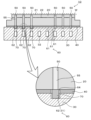
- FIG. 2 is a cross-sectional view taken along line AA in FIG. 1 .
- FIG. 4 is a partially enlarged cross-sectional view showing the periphery of the second gas passage 62 and the conductive gas passage 70.
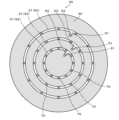
- 13 is a cross-sectional view of the wafer stage 10 cut along a horizontal plane passing through a second gas passage 62 as viewed from above.
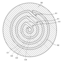
- FIG. 1 is a cross-sectional view of the wafer mounting table 10 cut by a horizontal plane passing through a coolant flow path 32 as viewed from above.
- FIG. 2 is an explanatory diagram in which a coolant flow path 32 and the like are drawn on a plan view of the wafer mounting table 10.
- 5A to 5C are diagrams showing the manufacturing process of the wafer mounting table 10.
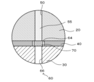
- FIG. 4 is a partially enlarged cross-sectional view showing the periphery of the second gas passage 62 and the conductive gas passage 70.
- 13 is a cross-sectional view of the wafer stage 10 cut along a
- FIG. 11 is a partially enlarged cross-sectional view showing another example of the conductive gas passage 70.
- 6 is a partially enlarged cross-sectional view showing another example of the conductive gas passage 70 and the gas introduction passage 60.
- FIG. 6 is a partially enlarged cross-sectional view showing another example of the conductive gas passage 70 and the gas introduction passage 60.
- FIG. FIG. 2 is an enlarged partial cross-sectional view showing a dense plug 155 and a conductive gas passage 170.
- FIG. 4 is a partially enlarged cross-sectional view showing the periphery of a conductive gas passage portion 270.
- FIG. 4 is a partially enlarged cross-sectional view showing the periphery of a conductive gas passage 370.
- FIG. 4 is a partially enlarged cross-sectional view showing the periphery of a conductive gas passage portion 470.
- FIG. 1 is a plan view of the wafer mounting table 10
- FIG. 2 is a cross-sectional view of FIG. 1
- FIG. 3 is a partially enlarged cross-sectional view showing the periphery of the second gas passage 62 and the conductive gas passage 70
- FIG. 4 is a cross-sectional view of the wafer mounting table 10 cut along a horizontal plane passing through the second gas passage 62
- FIG. 5 is a cross-sectional view of the wafer mounting table 10 cut along a horizontal plane passing through the refrigerant passage 32
- FIG. 6 is an explanatory diagram in which the refrigerant passage 32 and the like are drawn on the plan view of the wafer mounting table 10.
- FIG. 1 The partially enlarged view in FIG. 1 is an explanatory diagram in which the conductive gas passage 70 is drawn on the plan view of the wafer mounting table 10.
- FIG. 3 is a partially enlarged view of the cut surface of the wafer mounting table 10 cut along a vertical plane along the second gas passage 62 and a vertical plane passing through the conductive gas passage 70.
- “upper” and “lower” do not represent absolute positional relationships, but represent relative positional relationships. Therefore, depending on the orientation of the wafer placement table 10, "up” and “down” can become “down” and “up,” “left” and “right,” or "front” and “back.”
- the wafer mounting table 10 includes a ceramic plate 20, a conductive plate 30, a conductive bonding layer 40, a ceramic plate penetration 50, a gas introduction passage 60, and a conductive gas passage 70.
- the ceramic plate 20 is a ceramic disk (e.g., 300 mm in diameter, 5 mm in thickness) made of alumina sintered body or aluminum nitride sintered body.
- the upper surface of the ceramic plate 20 is a wafer mounting surface 21 on which the wafer W is placed.
- the ceramic plate 20 has an electrode 22 built in.
- a ring-shaped seal band 21a is formed along the outer edge of the wafer mounting surface 21 of the ceramic plate 20, and a plurality of small circular protrusions 21b are formed on the entire inner surface of the seal band 21a.
- the seal band 21a and the small circular protrusions 21b have the same height, and the height is, for example, several ⁇ m to several tens of ⁇ m.
- the electrode 22 is a planar mesh electrode used as an electrostatic electrode, and is connected to an external DC power source via a power supply member (not shown).
- a low-pass filter may be arranged in the middle of the power supply member.
- the power supply member is electrically insulated from the conductive bonding layer 40 and the conductive plate 30.
- the conductive plate 30 is a circular plate with good thermal conductivity (a circular plate with the same diameter as the ceramic plate 20 or a larger diameter). Inside the conductive plate 30, a refrigerant flow path 32 is formed through which a refrigerant circulates.
- the refrigerant flowing through the refrigerant flow path 32 is preferably a liquid, and is preferably electrically insulating. Examples of electrically insulating liquids include fluorine-based inert liquids.
- the refrigerant flow path 32 is formed in a single stroke from one end (inlet) to the other end (outlet) over the entire conductive plate 30 in a planar view. As shown in FIG.
- the refrigerant flow path 32 is arranged so that it runs from one end to the other end in a single stroke based on a multiple circle formed by arranging multiple imaginary circles (dotted and dashed circles C1 to C4, here C1 to C4 are concentric circles) with different diameters in a planar view so as not to overlap each other. Specifically, when the refrigerant flow path 32 is routed from one end to the other in a single stroke, the refrigerant is routed so as to trace the imaginary circles while connecting two imaginary circles that are in an inner and outer relationship among the multiple circles. One end and the other end of the refrigerant flow path 32 are connected to a supply port and a recovery port of an external refrigerant device (not shown), respectively.
- the refrigerant supplied to one end of the refrigerant flow path 32 from the supply port of the external refrigerant device passes through the refrigerant flow path 32, returns from the other end of the refrigerant flow path 32 to the recovery port of the external refrigerant device, and is supplied again from the supply port to one end of the refrigerant flow path 32 after being temperature-adjusted.
- the conductive plate 30 is connected to a radio frequency (RF) power source and is also used as an RF electrode.
- the material of the conductive plate 30 may be, for example, a metal material or a composite material of metal and ceramic.
- the metal material may be Al, Ti, Mo, or an alloy thereof.
- the composite material of metal and ceramic may be a metal matrix composite material (MMC) or a ceramic matrix composite material (CMC). Specific examples of such composite materials include a material containing Si, SiC, and Ti (also called SiSiCTi), a material in which a SiC porous body is impregnated with Al and/or Si, and a composite material of Al2O3 and TiC. It is preferable to select a material of the conductive plate 30 having a thermal expansion coefficient close to that of the material of the ceramic plate 20.
- the conductive bonding layer 40 is, for example, a metal bonding layer, and bonds the lower surface of the ceramic plate 20 and the upper surface of the conductive plate 30.
- the conductive bonding layer 40 is formed, for example, by TCB (thermal compression bonding).
- TCB is a known method in which a metal bonding material is sandwiched between two members to be joined, and the two members are pressure-bonded while being heated to a temperature below the solidus temperature of the metal bonding material.
- the ceramic plate penetration 50 is a hole that penetrates the ceramic plate 20 in the vertical direction.
- the ceramic plate penetration 50 is a gas passage that extends from the lower surface of the ceramic plate 20 to the reference surface 21c (FIG. 1) of the wafer mounting surface 21.
- a plurality of ceramic plate penetrations 50 (36 in this example) are provided.
- the ceramic plate penetration 50 has an electrically insulating porous plug 55 that allows gas to flow.
- the porous plug 55 is filled and fixed in the ceramic plate penetration 50.
- the outer peripheral surface of the porous plug 55 and the inner peripheral surface of the ceramic plate penetration 50 may be bonded, or the male screw portion provided on the outer peripheral surface of the porous plug 55 may be screwed into the female screw portion provided on the inner peripheral surface of the ceramic plate penetration 50.
- the upper surface of the porous plug 55 is at the same height as the reference surface 21c of the wafer mounting surface 21, and the lower surface of the porous plug 55 is at the same height as the lower surface of the ceramic plate 20.
- the porous plug 55 may be a porous bulk body obtained by sintering ceramic powder. Examples of ceramics that may be used include alumina and aluminum nitride.
- the porosity of the porous plug 55 is preferably 30% or more, and the average pore diameter is preferably 20 ⁇ m or more.
- the porosity of the porous plug 55 may be 70% or less.
- the gas introduction passage 60 is a gas passage provided at least inside the conductive plate 30 and communicates with the ceramic plate penetration 50.
- the gas introduction passage 60 includes a first gas passage 61, a second gas passage 62, a gas auxiliary passage 63 (FIG. 4), and a bonding layer penetration 64.
- the gas introduction passage 60 includes gas passages (first gas passage 61, second gas passage 62, and gas auxiliary passage 63) provided inside the conductive plate 30, and a gas passage (bonding layer penetration 64) provided inside the conductive bonding layer 40.
- the first gas passages 61 penetrate the conductive plate 30 in the vertical direction.
- the first gas passages 61 penetrate between the refrigerant flow paths 32 of the conductive plate 30 in the vertical direction.
- Multiple first gas passages 61 (three in this example) are provided.
- the second gas passage 62 is provided at the interface between the conductive bonding layer 40 and the conductive plate 30, parallel to the wafer mounting surface 21.
- “parallel” refers to a case where the second gas passage 62 is completely parallel, and also refers to a case where the second gas passage 62 is not completely parallel but is within a range of an allowable error (e.g., tolerance).
- the second gas passage 62 has a groove 31 (first recess) provided on the upper surface of the conductive plate 30, and is formed by covering the upper surface of the groove 31 with the conductive bonding layer 40. As shown in FIG. 6, the second gas passage 62 is provided in an annular shape so as to overlap with any of the multiple imaginary circles C1 to C4 in a plan view.
- the first second gas passage 62 from the outer periphery of the wafer mounting table 10 overlaps with the imaginary circle C1 with the largest diameter
- the second second gas passage 62 overlaps with the imaginary circle C2 with the second largest diameter
- the third intermediate gas passage 62 overlaps with the imaginary circle C3 with the third largest diameter.
- Each second gas passage 62 has an overlapping portion 62p (shaded portion in FIG. 6) that overlaps with the refrigerant flow path 32 along the refrigerant flow path 32 in a plan view.
- the gas auxiliary passage 63 is a passage that connects the first gas passage 61 and the second gas passage 62, and is provided at the interface between the conductive bonding layer 40 and the conductive plate 30 in parallel to the wafer mounting surface 21.
- a plurality of ceramic plate penetrations 50 (12 in this case) are provided for each second gas passage 62, but the number of first gas passages 61 and gas auxiliary passages 63 provided is less than the number of ceramic plate penetrations 50 (one for each second gas passage 62 in this case).
- the bonding layer penetration portion 64 is a hole that penetrates the conductive bonding layer 40 in the vertical direction.
- the bonding layer penetration portion 64 is a gas passage that reaches from the upper surface of the conductive plate 30 to the lower surface of the ceramic plate 20.
- a plurality of bonding layer penetration portions 64 (36 in this example) are provided, and are arranged in one-to-one correspondence with the ceramic plate penetration portions 50.
- the diameter of the bonding layer penetration portion 64 is the same as or larger than the diameter of the ceramic plate penetration portion 50.
- the diameter of the bonding layer penetration portion 64 is the same as or larger than the diameter of the conductive gas passage portion 70.
- the conductive gas passage 70 is provided in the gas introduction passage 60 and is provided so as to contact the lower surface of the porous plug 55.
- the conductive gas passage 70 is provided as a separate body from the conductive plate 30, and the lower surface is in contact with the conductive plate 30. More specifically, the conductive gas passage 70 is provided across the inside of the bonding layer penetration portion 64 and the inside of the second gas passage 62 in the gas introduction passage 60, and is in contact with the conductive plate 30 at a portion of the lower surface (bottom surface) of the second gas passage 62 (groove 31) located directly below the bonding layer penetration portion 64.
- the conductive gas passage 70 is electrically connected to the conductive plate 30 by contacting the conductive plate 30.
- a plurality of conductive gas passages 70 (36 in this embodiment) are provided, and are arranged in one-to-one correspondence with the porous plugs 55.
- the conductive gas passage 70 is a substantially cylindrical member that is circular when viewed from above.
- the conductive gas passage 70 is a member through which gas can pass. Therefore, the gas in the gas introduction passage 60 can pass through the conductive gas passage 70 and flow to the ceramic plate penetration 50.
- members through which gas can pass include a conductive mesh or a mass of conductive fibers.
- materials for the conductive gas passage 70 include metal materials and carbon. Examples of metal materials include Al, Ti, Mo, or alloys thereof, and steel. Examples of the mass of conductive fibers include steel wool or carbon felt.
- the mesh size may be 0.062 mm (250 mesh) to 0.154 mm (100 mesh).
- the conductive gas passage 70 is preferably an elastic member.
- the conductive mesh and conductive fiber mass described above are also examples of elastic members. If the conductive gas passage 70 has directional expansion and contraction, it is preferable that it is expandable at least in the vertical direction.
- the conductive gas passage 70 is preferably compressed by being pressed against the lower surface of the porous plug 55.
- the conductive gas passage 70 is an elastic member, and is compressed vertically between the porous plug 55 and the conductive plate 30 by being pressed against the lower surface of the porous plug 55.
- the conductive gas passage 70 is preferably arranged so as to overlap the entire lower surface of the porous plug 55 when viewed virtually from above.
- the diameter of the conductive gas passage 70 is larger than the diameter of the porous plug 55, and the entire lower surface of the porous plug 55 is included in the conductive gas passage 70 when viewed virtually from above.
- the conductive gas passage 70 preferably has a conductance larger than that of the porous plug 55, and more preferably has a conductance at least twice that of the porous plug 55.
- the conductance can be calculated, for example, by dividing the amount of gas (flow rate) flowing inside per unit time by the gas pressure difference between the inlet and outlet sides of the gas.
- the conductance of the conductive gas passage 70 can be adjusted, for example, by adjusting the mesh size when the conductive gas passage 70 is a conductive mesh, or by adjusting the thickness of the fibers and/or the void ratio inside the agglomerate when the conductive gas passage 70 is a conductive fiber aggregate.
- the wafer W is placed on the wafer mounting surface 21 with the wafer mounting table 10 installed in a chamber (not shown). Then, the chamber is depressurized by a vacuum pump to adjust the pressure inside the chamber to a predetermined degree of vacuum, and a DC voltage is applied to the electrode 22 of the ceramic plate 20 to generate an electrostatic adsorption force, and the wafer W is adsorbed and fixed to the wafer mounting surface 21 (specifically, the upper surface of the seal band 21a or the upper surface of the circular small protrusion 21b).
- the chamber is made into a reactive gas atmosphere with a predetermined pressure (for example, several tens to several hundreds of Pa), and in this state, an RF voltage is applied between an upper electrode (not shown) provided on the ceiling part of the chamber and the conductive plate 30 of the wafer mounting table 10 to generate plasma.
- the surface of the wafer W is treated by the generated plasma.
- a coolant is circulated through the coolant flow path 32 of the conductive plate 30.
- a backside gas is introduced from a gas cylinder (not shown) into the first gas passage 61 of the gas introduction passage 60.
- a thermally conductive gas e.g., He gas, etc.
- the backside gas introduced into the first gas passage 61 passes through the gas auxiliary passage 63, the second gas passage 62, and the conductive gas passage 70 in this order, and is distributed to the multiple ceramic plate penetrations 50, and is supplied to and sealed in the space between the back surface of the wafer W and the reference surface 21c of the wafer mounting surface 21.
- This backside gas allows efficient thermal conduction between the wafer W and the ceramic plate 20.
- the provision of a porous plug 55 in the ceramic plate penetration 50 can suppress discharge within the ceramic plate penetration 50. For example, if there is no porous plug 55, electrons generated as a result of ionization of gas molecules by application of an RF voltage accelerate and collide with other gas molecules, causing glow discharge and then arc discharge. However, if there is a porous plug 55, the electrons hit the porous plug 55 before colliding with other gas molecules, suppressing discharge.
- FIG. 7 is a manufacturing process diagram of the wafer mounting table 10.
- the conductive plate 30 is made of MMC.
- a ceramic plate 20 incorporating an electrode 22 is prepared (FIG. 7A).
- a ceramic powder compact incorporating the electrode 22 is made, and the compact is hot-pressed and fired to obtain the ceramic plate 20.
- a ceramic plate penetration 50 is formed in the ceramic plate 20 (FIG. 7B). The ceramic plate penetration 50 is formed to penetrate the ceramic plate 20 in the vertical direction, avoiding the electrode 22.
- two MMC disk members 81, 82 are prepared (Fig. 7C). Then, by machining, grooves and holes are appropriately formed in these MMC disk members 81, 82 (Fig. 7D). Specifically, a groove 32a that will eventually become the refrigerant flow path 32 is formed on the lower surface of the upper MMC disk member 81, and a groove 31 that will eventually become the second gas passage 62 is formed on the upper surface of the MMC disk member 81. In addition, a through hole 61a that will eventually become part of the first gas passage 61 is formed so as to reach the lower surface of the MMC disk member 81.
- a through hole 61b that will eventually become part of the first gas passage 61 is formed in the lower MMC disk member 82.
- the MMC disk members 81, 82 are made of SiSiCTi or AlSiC. This is because the thermal expansion coefficient of alumina can be made roughly the same as that of SiSiCTi or AlSiC.
- the SiSiCTi disk member can be produced, for example, as follows. First, silicon carbide, metallic Si, and metallic Ti are mixed to produce a powder mixture. Next, the resulting powder mixture is uniaxially pressed to produce a disk-shaped compact, which is then hot-press sintered in an inert atmosphere to obtain the SiSiCTi disk member.
- the ceramic plate 20, the MMC disk member 81, and the MMC disk member 82 are bonded by TCB, the overall shape is adjusted, and the porous plug 55 is attached to obtain the wafer mounting table 10 (FIGS. 7E and 7F).
- a metal bonding material 83 is sandwiched between the upper surface of the lower MMC disk member 82 and the lower surface of the upper MMC disk member 81, and a metal bonding material 90 is sandwiched between the upper surface of the upper MMC disk member 81 and the lower surface of the ceramic plate 20 to obtain a laminate.
- a through hole that will eventually become part of the first gas passage 61 is formed in advance in the metal bonding material 83, and a through hole that will eventually become the bonding layer penetration portion 64 is formed in advance in the metal bonding material 90.
- the metal bonding material 90 is placed on the upper surface of the MMC disk member 81, the conductive gas passage portion 70 is inserted in advance into the through hole that will become the bonding layer penetration portion 64 and into the recessed groove 31 directly below it.
- the laminate is pressed and bonded at a temperature below the solidus temperature of the metal bonding materials 83, 90 (for example, at a temperature equal to or higher than the solidus temperature minus 20°C and below the solidus temperature), and then returned to room temperature.
- the two MMC disk members 81, 82 are bonded by the metal bonding material 83 to form the conductive plate 30.
- the ceramic plate 20 and the conductive plate 30 are also bonded by the metal bonding material 90.
- the metal bonding material 90 becomes the conductive bonding layer 40.
- As the metal bonding materials 83, 90 Al-Mg-based bonding materials and Al-Si-Mg-based bonding materials can be used. For example, when TCB is performed using an Al-Si-Mg-based bonding material, the laminate is pressed in a heated state under a vacuum atmosphere. It is preferable to use metal bonding materials 83, 90 with a thickness of about 100 ⁇ m.
- the porous plug 55 may be attached, for example, by preparing a porous plug 55 formed in advance by firing, applying an adhesive to the ceramic plate penetration portion 50, and then inserting the porous plug 55 from above the ceramic plate penetration portion 50 to adhesively fix the outer peripheral surface of the porous plug 55 to the inner peripheral surface of the ceramic plate penetration portion 50.
- a male thread portion may be formed on the outer peripheral surface of the porous plug 55
- a female thread portion may be formed on the inner peripheral surface of the ceramic plate penetration portion 50
- the porous plug 55 may be screwed into the ceramic plate penetration portion 50 to screw the male thread portion of the porous plug 55 into the female thread portion of the ceramic plate penetration portion 50, thereby attaching the porous plug 55.
- the porous plug 55 When the porous plug 55 is inserted into the ceramic plate penetration 50, the porous plug 55 may be inserted not only until it contacts the conductive gas passage 70, but also until it presses the conductive gas passage 70 downward to compress the conductive gas passage 70. In this way, the conductive gas passage 70 can be more reliably brought into contact with the lower surface of the porous plug 55. In addition, since the conductive gas passage 70 is in a compressed state in the wafer mounting table 10 after manufacture, the contact between the conductive gas passage 70 and the porous plug 55 is more easily maintained. In this case, for example, the conductive gas passage 70 may be arranged so that the upper end of the conductive gas passage 70 is inserted inside the ceramic plate penetration 50 before the porous plug 55 is attached (before the conductive gas passage 70 is compressed). In this way, the conductive gas passage 70 can be easily pressed by the porous plug 55 when the porous plug 55 is inserted.
- the conductive gas passage 70 is provided in the gas introduction passage 60 (here, in the second gas passage 62 and the bonding layer penetration portion 64), contacts the lower surface of the porous plug 55, and is electrically conductive with the conductive plate 30. Therefore, since the conductive gas passage 70, which has the same potential as the conductive plate 30, contacts the porous plug 55, discharge can be suppressed around the end of the porous plug 55 on the conductive plate 30 side, i.e., around the lower end of the porous plug 55. Note that, for example, even if an insulating porous member is present on the lower surface of the porous plug 55 instead of the conductive gas passage 70, discharge can be suppressed around the lower end of the porous plug 55.
- the presence of the conductive gas passage 70 makes it difficult for a potential difference to occur around the end of the porous plug 55 on the conductive plate 30 side, and discharge can be suppressed more effectively.
- the power of the radio frequency (RF) power source connected to the conductive plate 30 can be increased, for example, compared to the case where an insulating porous member is present instead of the conductive gas passage 70.
- RF radio frequency
- discharge can be further suppressed by the conductive gas passage 70, so the gas pressure can be increased compared to when an insulating porous member is used instead of the conductive gas passage 70.
- discharge can be suppressed even if the internal space (gap) of the conductive gas passage 70 is larger than the pores of the insulating porous member, so that gas filling is completed quickly and the gas pressure can be easily controlled to a constant value.
- the conductive gas passage 70 is a separate member from the conductive plate 30 and is in contact with the gas introduction passage 60. Therefore, the wafer mounting table 10 is easier to manufacture than, for example, when the conductive gas passage 70 is an integral member with the conductive plate 30 rather than a separate member.
- the conductive gas passage 70 is an elastic member, and is pressed and compressed against the lower surface of the porous plug 55. Therefore, contact between the conductive gas passage 70 and the porous plug 55 is easily maintained.
- the conductive gas passage 70 is formed of a conductive mesh or a mass of conductive fibers. Therefore, gas can easily flow through the inside of the conductive gas passage 70.
- the conductive gas passage 70 is arranged so as to overlap the entire lower surface of the porous plug 55 when viewed virtually from above. Therefore, the conductive gas passage 70 is present on the lower side with respect to the entire lower surface of the porous plug 55, so that discharge around the end of the porous plug 55 on the conductive plate 30 side can be more reliably suppressed.
- the conductive gas passage 70 may be a conductive bulk body having holes that open toward the lower surface of the porous plug 55 and allow gas to pass in the vertical direction.
- the conductive gas passage 70 may be a conductive bulk body having holes 70a that open toward the lower surface of the porous plug 55 and allow gas to pass in the vertical direction, and a groove 70b that is provided on the lower surface of the conductive gas passage 70 and opens horizontally to the second gas passage 62.
- the lower surface of the conductive gas passage 70 in FIG. 8 is in contact with the conductive plate 30. This conductive gas passage 70 allows gas to pass through the internal holes 70a and grooves 70b.
- the diameter of the hole 70a is preferably 0.1 mm or more and 1 mm or less. If the diameter of the hole 70a is 0.1 mm or more, the gas flow rate is unlikely to be insufficient. Also, if the diameter of the hole 70a is 1 mm or less, a potential difference is unlikely to occur in the hole 70a, and discharge in the hole 70a can be suppressed.
- the width and depth of the groove 70b are also preferably 0.1 mm or more from the viewpoint of the gas flow rate. Although the width and depth of the groove 70b are unlikely to affect the discharge, the width and depth of the groove 70b may be 1 mm or less. At least one of the holes 70a and the grooves 70b may be provided in multiple numbers.
- the conductive bulk body may also be made of a composite material of metal and ceramic listed as the materials of the conductive plate 30.
- the conductive gas passage 70 and the conductive plate 30 may be made of the same material.
- the conductance of the conductive gas passage 70 can be adjusted, for example, by adjusting the size and/or number of at least one of the holes 70a and the grooves 70b.
- the conductive gas passage 70 may be an integral member rather than a separate member from the conductive plate 30.
- the conductive gas passage 70 of the conductive bulk body shown in FIG. 8 may be part of the conductive plate 30.
- the conductive gas passage 70 is formed as a protrusion provided on the upper surface of the conductive plate 30.
- the conductive gas passage 70 may be a conductive porous body.
- the conductive porous material may be SiC or SiSiC.
- the conductive porous body may have an average pore diameter of 0.05 mm or more and 1 mm or less. If the average pore diameter is 0.05 mm or more, the gas flow rate is less likely to be insufficient. If the average pore diameter is 1 mm or less, a potential difference is less likely to occur within the conductive porous body, and discharge within the conductive porous body can be suppressed.
- the porosity of the conductive porous body may be 30% or more, or 70% or less.
- the second gas passage 62 has a groove 31 (first recess) provided on the upper surface of the conductive plate 30, and is formed by placing the lower surface (flat surface) of the conductive bonding layer 40 on the groove 31, but is not limited to this.
- the second gas passage 62 may be formed by having a groove (second recess) provided on the lower surface of the conductive bonding layer 40 and placing the upper surface (flat surface) of the conductive plate 30 below the groove.
- the conductive bonding layer 40 may have a two-layer structure, with a groove (groove penetrating in the vertical direction) that will eventually become the second gas passage 62 provided in the lower layer, and the above-mentioned bonding layer penetration portion 64 provided in the upper layer.
- a conductive gas passage portion 70 is provided inside the gas introduction passage 60 (bonding layer penetration portion 64), and the conductive gas passage portion 70 is provided so as to contact the lower surface of the porous plug 55 and to be electrically conductive with the conductive plate 30, thereby suppressing discharge around the end of the porous plug 55 on the conductive plate 30 side.
- the second gas passage 62 may be built into the conductive plate 30 instead of being provided at the interface between the conductive bonding layer 40 and the conductive plate 30.
- the second gas passage 62 may be built into the conductive plate 30, and the third gas passage 65, which is a vertical hole that connects the second gas passage 62 and the bonding layer penetration portion 64, may be provided in the conductive plate 30.
- the presence of the conductive gas passage 70 can suppress discharge around the end of the porous plug 55 on the conductive plate 30 side.
- a first MMC disk member having a through hole that becomes the third gas passage 65 and a second MMC disk member having a groove 32a that becomes the refrigerant flow path 32 and a through hole 61a that becomes part of the first gas passage 61 may be used instead of the MMC disk member 81 shown in FIG.
- At least one of the lower surface of the first MMC disc member and the upper surface of the second MMC disc member should have a groove that serves as the second gas passage 62.
- the second gas passage 62 and the auxiliary gas passage 63 may be omitted, and the multiple first gas passages 61 may be connected one-to-one to the multiple ceramic plate penetrations 50.
- the gas flowing horizontally through the second gas passage 62 flows into the conductive gas passage 70, but the direction of the gas flow is not limited to this.
- the gas introduction passage 60 may have a fourth gas passage 66 that is provided directly below the conductive gas passage 70 and has a diameter smaller than that of the conductive gas passage 70, and the gas flowing upward from the fourth gas passage 66 may flow into the conductive gas passage 70.
- the conductive gas passage 70 in FIG. 10 is disposed inside the bonding layer penetration portion 64 of the gas introduction passage 60 and is in contact with the lower surface of the porous plug 55 and the upper surface of the conductive plate 30.
- the fourth gas passage 66 may be a hole that communicates with the second gas passage 62, similar to the third gas passage 65 in FIG. 9.
- the second gas passage 62 and the auxiliary gas passage 63 are omitted in the gas introduction passage 60, and the fourth gas passage 66 may be a hole that communicates with the first gas passage 61 or a part of the first gas passage 61.
- the diameter of the conductive gas passage 70 may be the same as the diameter of the porous plug 55. Even in this case, if the conductive gas passage 70 and the porous plug 55 are arranged so that their contours match when viewed virtually from above, the conductive gas passage 70 can be arranged so that it overlaps the entire lower surface of the porous plug 55. Also, the diameter of the conductive gas passage 70 may be smaller than the diameter of the porous plug 55. In this case, the diameter of the bonding layer penetration portion 64 may be made smaller than the diameter of the porous plug 55 so that part of the lower surface of the porous plug 55 comes into contact with the upper surface of the conductive bonding layer 40.
- the conductive gas passage 70 is a generally cylindrical member that is circular when viewed from above, but is not limited to this.
- the conductive gas passage 70 may be a generally rectangular parallelepiped (including cubic) member.
- the conductive gas passage 70 is electrically connected to the conductive plate 30 by contacting the conductive plate 30, but this is not particularly limited.
- the conductive gas passage 70 may be in contact with the conductive bonding layer 40 while being separated from the conductive plate 30, and the conductive gas passage 70 may be electrically connected to the conductive plate 30 via the conductive bonding layer 40.
- the upper surface of the porous plug 55 is at the same height as the reference surface 21c of the wafer mounting surface 21, but is not limited to this.
- the difference between the height of the reference surface 21c of the wafer mounting surface 21 and the height of the upper surface of the porous plug 55 may be in the range of 0.5 mm or less (preferably 0.2 mm or less, more preferably 0.1 mm or less).
- the upper surface of the porous plug 55 may be located at a position lower than the reference surface 21c of the wafer mounting surface 21 by 0.5 mm or less (preferably 0.2 mm or less, more preferably 0.1 mm or less). Even in this way, the height of the space between the lower surface of the wafer W and the upper surface of the porous plug 55 is kept relatively low. Therefore, it is possible to prevent glow discharge and therefore arc discharge from occurring in this space.
- the lower surface of the porous plug 55 is at the same height as the lower surface of the ceramic plate 20, but this is not particularly limited.
- the lower end of the porous plug 55 may protrude below the lower surface of the ceramic plate 20, or the lower end of the porous plug 55 may be located above the lower surface of the ceramic plate 20 and the conductive gas passage 70 may be in contact with the lower surface of the porous plug 55 inside the ceramic plate penetration 50.
- the porous plug 55 prepared in advance is inserted into the ceramic plate penetration portion 50, but this is not particularly limited.
- a paste-like ceramic mixture that serves as a precursor of the porous plug 55 may be injected into the ceramic plate penetration portion 50 of the ceramic plate 20 and fired to form the porous plug 55.
- the underside of the porous plug 55 may be brought into contact with the conductive gas passage portion 70.
- the ceramic plate penetration portion 50 is provided with a porous plug 55, but the ceramic plate penetration portion 50 may be provided with an insulating gas-permeable plug through which gas can pass, not limited to a porous body such as the porous plug 55.
- an electrically insulating dense plug 155 having an internal gas flow path 155a as shown in FIG. 11 may be used as the insulating gas-permeable plug.
- the internal gas flow path 155a is a flow path that allows gas to flow between the upper and lower sides of the dense plug 155.
- the internal gas flow path 155a is a passage that passes through the upper and lower sides of the dense plug 155 while bending, and is more specifically configured as a spiral passage.
- the internal gas flow path 155a may be a straight through hole along the vertical direction.
- the diameter of the cross section of the internal gas flow path 155a is preferably 0.1 mm or more and 1 mm or less.
- One dense plug 155 may have multiple internal gas flow paths 155a.
- the porosity of the dense portion of the dense plug 155 is preferably less than 0.1%.
- the dense plug 155 may be made of ceramics such as alumina or aluminum nitride, as in the case of the porous plug 55.
- the dense plug 155 may be manufactured by firing a molded body formed using a 3D printer, or by firing a molded body formed by mold casting.
- the conductive gas passage 70 may be a coating layer that covers the lower surface of the insulating gas passage plug.
- the conductive gas passage 170 shown in FIG. 11 is formed as a coating layer that covers the lower surface of the dense plug 155.
- the conductive gas passage 170 is formed as a dense layer and has holes 170a that allow gas to pass in the vertical direction. The holes 170a connect the opening of the internal gas flow path 155a on the lower surface of the dense plug 155 to the gas introduction passage 60.
- the conductive gas passage 170 can be manufactured, for example, by forming a coating layer on the lower surface of the dense plug 155 by sputtering or electroless plating before attaching the dense plug 155 to the ceramic plate 20, and opening the holes 170a.
- the material of the conductive gas passage 170 can be, for example, a metal material, and metals with excellent corrosion resistance such as Au, Ag, and Al are preferable. Even when the conductive gas passage 170 is a coating layer that covers the lower surface of the dense plug 155, the conductive gas passage 170 contacts the lower surface of the dense plug 155 and is electrically connected to the conductive plate 30, so that discharge around the lower end of the dense plug 155 can be suppressed.
- the diameter of the hole 170a is preferably 0.1 mm or more and 1 mm or less.
- the conductive gas passage 170 is not in direct contact with the conductive plate 30, but is in contact with the conductive bonding layer 40 and is electrically connected to the conductive plate 30 via the conductive bonding layer 40.
- the conductive gas passage 170 is not limited to a dense layer and may be a porous layer. In this case, if gas can pass through the pores inside the conductive gas passage 170, there is no need to form the holes 170a.
- the conductive gas passage 170 can be formed as a metal porous layer on the lower surface of the dense plug 155.
- the lower surface of the dense plug 155 is covered with the conductive gas passage 170, but the conductive gas passage 170 may be formed so as to cover the lower surface of the porous plug 55.
- the conductive gas passage 170 is preferably a porous layer.
- the conductive gas passage portion 70 has been described as a single member, but the conductive gas passage portion 70 may be composed of multiple members.
- the conductive gas passage portion 70 may have one or more of the above-mentioned elastic member, conductive mesh, conductive fiber mass, conductive bulk body, conductive porous body, and a coating layer that covers the lower surface of the insulating gas passage plug, and may have two or more different types of members in combination, or may have two or more members of the same type.
- the conductive gas passage portion 70 has multiple members in this way, it is sufficient that the multiple members are electrically conductive with each other, the conductive gas passage portion 70 as a whole is electrically conductive with the conductive plate, and gas can pass through the inside. Also, if the conductive gas passage portion 70 has multiple members, it is sufficient that any of the multiple members is in contact with the lower surface of the insulating gas passage plug.
- the conductive gas passage section 70 is composed of multiple members including an elastic member, it is sufficient that the elastic member is compressed by pressing the conductive gas passage section 70 against the bottom surface of the insulating gas passage plug, and it is not necessary for the elastic member to be pressed in direct contact with the bottom surface of the insulating gas passage plug.
- the conductive gas passage may have a structure in which one or more conductive meshes and one or more conductive sheets having holes through which gas can pass in the vertical direction are stacked.
- the conductive gas passage 270 shown in FIG. 12 has a plurality of conductive gas passage members, specifically, a plurality (two in this case) of meshes 271 and a plurality (two in this case) of conductive sheets 272.
- the plurality of meshes 271 and the plurality of conductive sheets 272 are stacked alternately in the vertical direction.
- the mesh 271 can be made of the same material as the conductive mesh given as an example of the conductive gas passage 70 described above.
- the conductive sheet 272 is also an example of a conductive bulk body, and can be made of the same material as the conductive gas passage 70, which is a conductive bulk body shown in FIG. 8.
- the conductive sheet 272 only needs to have one or more holes 272a through which gas can pass in the vertical direction, and in FIG. 12, the conductive sheet 272 has a plurality of holes 272a (only three are shown).
- the diameter of the hole 272a is preferably 0.1 mm or more and 1 mm or less, similar to the hole 70a.
- the thickness of the conductive sheet 272 may be, for example, 0.01 mm or more and 2 mm or less.
- the conductive gas passage 270 In the conductive gas passage 270, the upper surface of the mesh 271 located at the top is in contact with the lower surface of the porous plug 55, and the lower surface of the conductive sheet 272 located at the bottom is in contact with the conductive plate 30. All of the meshes 271 are pressed against the lower surface of the porous plug 55 and compressed.
- the conductive gas passage 270 may include the above-mentioned conductive porous body instead of the conductive sheet 272. That is, the conductive gas passage 270 may have a structure in which one or more meshes 271 and one or more conductive porous bodies are stacked in the vertical direction.
- the conductive gas passage 270 has a structure in which a member having elasticity such as the mesh 271 and a member having no elasticity such as the conductive sheet 272 or the conductive porous body are stacked, the thickness of the entire conductive gas passage 270 can be easily adjusted to a desired value depending on the thickness of the member having no elasticity.
- the conductive gas passage 270 may be a laminate in which multiple meshes 271 are stacked vertically without the conductive sheet 272.
- the conductive gas passage may have a plurality of conductive gas passage members including a coating layer that covers the lower surface of the insulating gas passage plug.
- the conductive gas passage 370 shown in FIG. 13 has a coating layer 371 and a mesh 372 as a plurality of conductive gas passage members.
- the coating layer 371 covers the lower surface of the dense plug 155, similar to the conductive gas passage 170 in FIG. 11.
- the coating layer 371 has holes 371a similar to the holes 170a.
- the upper surface of the mesh 372 is in contact with the lower surface of the coating layer 371.
- the mesh 372 can be made of a material similar to the conductive mesh given as an example of the conductive gas passage 70 described above.
- the coating layer 371 is in contact with the lower surface of the dense plug 155, and the lower surface of the mesh 372 is in contact with the conductive plate 30.
- the conductive gas passage 370 may have any of an elastic member, a mass of conductive fibers, a conductive bulk body, and a conductive porous body.
- the ceramic plate 20 and the conductive plate 30 are joined by the conductive bonding layer 40, but a non-conductive bonding layer such as a resin bonding layer may be used instead of the conductive bonding layer 40.
- a non-conductive bonding layer such as a resin bonding layer may be used instead of the conductive bonding layer 40.
- metals such as Al and Ti can be used for the conductive plate.
- the ceramic plate 20 has an electrostatic electrode built in as the electrode 22, but instead of or in addition to this, a heater electrode (resistance heating element) may be built in. In this case, a heater power supply is connected to the heater electrode.
- the ceramic plate 20 may have one layer of electrodes built in, or two or more layers spaced apart.
- lift pin holes may be provided that penetrate the wafer mounting table 10.
- the lift pin holes are holes for inserting lift pins that raise and lower the wafer W relative to the wafer mounting surface 21.
- the lift pin holes are provided in three locations.
- the ceramic plate 20 was produced by hot-pressing and firing a ceramic powder compact, but the compact may also be produced by stacking multiple tape compacts, by mold casting, or by compressing ceramic powder.
- the conductive gas passage portion 70 may be an elastic body.
- the elastic body include a conductive spring.
- the spring may be made of the metal materials (Al, Ti, Mo or alloys thereof, steel) mentioned in the above-mentioned embodiment. It is preferable that the elastic body is disposed in a state in which it presses the insulating gas passage plug upward with its elastic force. In this way, contact between the conductive gas passage portion and the insulating gas passage plug is easily maintained.
- the above-mentioned conductive gas passage portion 70 has a plurality of conductive gas passage members, one or more of the plurality of conductive gas passage members may be an elastic body.
- the conductive gas passage portion 70 may have an elastic body and one or more of the various members described above.
- the conductive gas passage portion 70 has a plurality of conductive gas passage members including an elastic body, it is not necessary for the elastic body itself to directly contact and press the insulating gas passage plug, and it is sufficient that the conductive gas passage portion 70 presses the insulating gas passage plug upward with the elastic force of the elastic body.
- the conductive gas passage may have a coating layer that covers the lower surface of the insulating gas passage plug and an elastic body that presses the coating layer upward with an elastic force.
- the conductive gas passage 470 shown in FIG. 14 has a coating layer 471 and an elastic body 472 as a plurality of conductive gas passage members.
- the coating layer 471 contacts the lower surface of the dense plug 155 by covering the lower surface of the dense plug 155, similar to the conductive gas passage 170 in FIG. 11 and the coating layer 371 in FIG. 13.
- the coating layer 471 has a hole 471a similar to the hole 371a.
- the coating layer 471 is a layer formed in advance by sputtering on the lower surface of the dense plug 155, and is made of Ti.
- the material of the coating layer 471 may be the same as the coating layer 170 described above.
- the elastic body 472 is a conductive spring, and the upper surface of the elastic body 472 contacts the lower surface of the dense plug 155. The lower surface of the elastic body 472 is in contact with the conductive plate 30.
- the elastic body 472 allows gas to pass through the inside. Specifically, gas can pass through the direction along the central axis of the elastic body 472 (up and down direction) and between the wires of the springs constituting the elastic body 472.
- the elastic body 472 is disposed inside the wafer mounting table 10 in a state compressed from its natural length, and presses the coating layer 471 and the dense plug 155 upward with its elastic force.
- the elastic body 472 presses the conductive plate 30 downward with its elastic force.
- the coating layer 471 and the elastic body 472 are in contact with each other and are electrically conductive, and the elastic body 472 and the conductive plate 30 are in contact with each other and are electrically conductive.
- the elastic body 472 presses the lower surface of the coating layer 471 upward with its elastic force, so that the contact between the conductive gas passage 470 and the dense plug 155 is easily maintained.
- the porous plug 55 is screwed to the ceramic plate 20.
- a paste-like ceramic mixture that is a precursor of the porous plug 55 is injected into the ceramic plate 20 and then fired to form the porous plug 55.
- the porous plug 55 and the ceramic plate 20 are in direct contact with each other.
- the insulating gas-permeable plug may be provided in the ceramic plate through-hole so as to be in direct contact with the ceramic plate. In this way, it is not necessary to use an adhesive such as a resin to bond the insulating gas-permeable plug and the ceramic plate.
- the insulating gas-permeable plug may be a member having a shape (e.g., a truncated cone) in which the area of the lower surface is larger than that of the upper surface.
- the ceramic plate is formed so that the ceramic plate through-hole has a shape that matches the insulating gas-permeable plug (a shape in which the cross-sectional area of the lower surface is larger than that of the upper surface), and the ceramic plate and the conductive plate are joined after the insulating gas-permeable plug is inserted into the ceramic plate through-hole from the lower surface of the ceramic plate in advance.
- the insulating gas-permeable plug can be provided in the ceramic plate through-hole so as to be in direct contact with the ceramic plate, and no adhesive is required.
- the present invention can be used, for example, in devices for processing wafers.
Landscapes
- Container, Conveyance, Adherence, Positioning, Of Wafer (AREA)
Priority Applications (4)
| Application Number | Priority Date | Filing Date | Title |
|---|---|---|---|
| KR1020247008103A KR102772614B1 (ko) | 2023-01-26 | 2023-08-31 | 웨이퍼 적재대 |
| CN202380013320.8A CN120513512A (zh) | 2023-01-26 | 2023-08-31 | 晶片载放台 |
| JP2024509335A JP7618098B2 (ja) | 2023-01-26 | 2023-08-31 | ウエハ載置台 |
| US18/582,759 US20240297062A1 (en) | 2023-01-26 | 2024-02-21 | Wafer placement table |
Applications Claiming Priority (2)
| Application Number | Priority Date | Filing Date | Title |
|---|---|---|---|
| JPPCT/JP2023/002417 | 2023-01-26 | ||
| JP2023002417 | 2023-01-26 |
Related Child Applications (1)
| Application Number | Title | Priority Date | Filing Date |
|---|---|---|---|
| US18/582,759 Continuation US20240297062A1 (en) | 2023-01-26 | 2024-02-21 | Wafer placement table |
Publications (1)
| Publication Number | Publication Date |
|---|---|
| WO2024157518A1 true WO2024157518A1 (ja) | 2024-08-02 |
Family
ID=91970183
Family Applications (1)
| Application Number | Title | Priority Date | Filing Date |
|---|---|---|---|
| PCT/JP2023/031890 Ceased WO2024157518A1 (ja) | 2023-01-26 | 2023-08-31 | ウエハ載置台 |
Country Status (6)
| Country | Link |
|---|---|
| US (1) | US20240297062A1 (https=) |
| JP (1) | JP7618098B2 (https=) |
| KR (1) | KR102772614B1 (https=) |
| CN (1) | CN120513512A (https=) |
| TW (1) | TW202431469A (https=) |
| WO (1) | WO2024157518A1 (https=) |
Cited By (1)
| Publication number | Priority date | Publication date | Assignee | Title |
|---|---|---|---|---|
| WO2026058633A1 (ja) * | 2024-09-12 | 2026-03-19 | 日本碍子株式会社 | ウエハ載置台 |
Families Citing this family (1)
| Publication number | Priority date | Publication date | Assignee | Title |
|---|---|---|---|---|
| KR102810844B1 (ko) * | 2023-02-06 | 2025-05-22 | 엔지케이 인슐레이터 엘티디 | 서셉터 |
Citations (3)
| Publication number | Priority date | Publication date | Assignee | Title |
|---|---|---|---|---|
| JP2019519927A (ja) * | 2016-06-07 | 2019-07-11 | アプライド マテリアルズ インコーポレイテッドApplied Materials,Incorporated | ガス孔に開口縮小プラグを有する大電力静電チャック |
| JP2020150071A (ja) * | 2019-03-12 | 2020-09-17 | 新光電気工業株式会社 | 基板固定装置 |
| WO2021241645A1 (ja) * | 2020-05-28 | 2021-12-02 | 京セラ株式会社 | 通気性プラグ、基板支持アセンブリおよびシャワープレート |
Family Cites Families (8)
| Publication number | Priority date | Publication date | Assignee | Title |
|---|---|---|---|---|
| KR20090097229A (ko) * | 2008-03-11 | 2009-09-16 | 전영재 | 반도체 및 lcd 제조용 정전척 |
| US8336891B2 (en) * | 2008-03-11 | 2012-12-25 | Ngk Insulators, Ltd. | Electrostatic chuck |
| JP5984504B2 (ja) * | 2012-05-21 | 2016-09-06 | 新光電気工業株式会社 | 静電チャック、静電チャックの製造方法 |
| JP5633766B2 (ja) * | 2013-03-29 | 2014-12-03 | Toto株式会社 | 静電チャック |
| US10688750B2 (en) * | 2017-10-03 | 2020-06-23 | Applied Materials, Inc. | Bonding structure of E chuck to aluminum base configuration |
| KR102188779B1 (ko) * | 2018-10-15 | 2020-12-08 | 세메스 주식회사 | 기판 지지 장치 및 그 제조방법 |
| JP7402411B2 (ja) | 2018-10-30 | 2023-12-21 | Toto株式会社 | 静電チャック |
| JP7600025B2 (ja) * | 2021-04-23 | 2024-12-16 | 新光電気工業株式会社 | 静電吸着部材及び基板固定装置 |
-
2023
- 2023-08-31 CN CN202380013320.8A patent/CN120513512A/zh active Pending
- 2023-08-31 WO PCT/JP2023/031890 patent/WO2024157518A1/ja not_active Ceased
- 2023-08-31 KR KR1020247008103A patent/KR102772614B1/ko active Active
- 2023-08-31 JP JP2024509335A patent/JP7618098B2/ja active Active
- 2023-09-13 TW TW112134834A patent/TW202431469A/zh unknown
-
2024
- 2024-02-21 US US18/582,759 patent/US20240297062A1/en active Pending
Patent Citations (3)
| Publication number | Priority date | Publication date | Assignee | Title |
|---|---|---|---|---|
| JP2019519927A (ja) * | 2016-06-07 | 2019-07-11 | アプライド マテリアルズ インコーポレイテッドApplied Materials,Incorporated | ガス孔に開口縮小プラグを有する大電力静電チャック |
| JP2020150071A (ja) * | 2019-03-12 | 2020-09-17 | 新光電気工業株式会社 | 基板固定装置 |
| WO2021241645A1 (ja) * | 2020-05-28 | 2021-12-02 | 京セラ株式会社 | 通気性プラグ、基板支持アセンブリおよびシャワープレート |
Cited By (1)
| Publication number | Priority date | Publication date | Assignee | Title |
|---|---|---|---|---|
| WO2026058633A1 (ja) * | 2024-09-12 | 2026-03-19 | 日本碍子株式会社 | ウエハ載置台 |
Also Published As
| Publication number | Publication date |
|---|---|
| KR102772614B1 (ko) | 2025-02-26 |
| JP7618098B2 (ja) | 2025-01-20 |
| US20240297062A1 (en) | 2024-09-05 |
| JPWO2024157518A1 (https=) | 2024-08-02 |
| CN120513512A (zh) | 2025-08-19 |
| KR20240119246A (ko) | 2024-08-06 |
| TW202431469A (zh) | 2024-08-01 |
Similar Documents
| Publication | Publication Date | Title |
|---|---|---|
| JP7618098B2 (ja) | ウエハ載置台 | |
| JP7759834B2 (ja) | ウエハ載置台 | |
| US20250336655A1 (en) | Wafer placement table | |
| WO2024069742A1 (ja) | ウエハ載置台 | |
| JP7583698B2 (ja) | ウエハ載置台 | |
| JP2025109922A (ja) | ウエハ載置台 | |
| US20240355656A1 (en) | Wafer placement table | |
| JP7573117B1 (ja) | ウエハ載置台 | |
| JP7776669B1 (ja) | ウエハ載置台 | |
| KR20240060512A (ko) | 웨이퍼 배치대 | |
| WO2024004040A1 (ja) | ウエハ載置台 | |
| JP7747847B1 (ja) | ウエハ載置台 | |
| US20250299935A1 (en) | Wafer placement table | |
| WO2026058633A1 (ja) | ウエハ載置台 | |
| JP7621458B2 (ja) | ウエハ載置台 | |
| JP7780062B1 (ja) | ウエハ載置台 | |
| JP7809252B1 (ja) | ウエハ載置台 | |
| JP7713116B1 (ja) | 半導体製造装置用部材 | |
| JP7606598B2 (ja) | ウエハ載置台 | |
| KR20260057603A (ko) | 웨이퍼 배치대 | |
| JP2026034822A (ja) | 半導体製造装置用部材 |
Legal Events
| Date | Code | Title | Description |
|---|---|---|---|
| WWE | Wipo information: entry into national phase |
Ref document number: 2024509335 Country of ref document: JP |
|
| WWE | Wipo information: entry into national phase |
Ref document number: 202380013320.8 Country of ref document: CN |
|
| 121 | Ep: the epo has been informed by wipo that ep was designated in this application |
Ref document number: 23918478 Country of ref document: EP Kind code of ref document: A1 |
|
| WWP | Wipo information: published in national office |
Ref document number: 202380013320.8 Country of ref document: CN |
|
| NENP | Non-entry into the national phase |
Ref country code: DE |
|
| 122 | Ep: pct application non-entry in european phase |
Ref document number: 23918478 Country of ref document: EP Kind code of ref document: A1 |