WO2024150673A1 - 混合組成物及び有機電界発光素子 - Google Patents
混合組成物及び有機電界発光素子 Download PDFInfo
- Publication number
- WO2024150673A1 WO2024150673A1 PCT/JP2023/046770 JP2023046770W WO2024150673A1 WO 2024150673 A1 WO2024150673 A1 WO 2024150673A1 JP 2023046770 W JP2023046770 W JP 2023046770W WO 2024150673 A1 WO2024150673 A1 WO 2024150673A1
- Authority
- WO
- WIPO (PCT)
- Prior art keywords
- general formula
- group
- compound represented
- substituted
- mixed composition
- Prior art date
- Legal status (The legal status is an assumption and is not a legal conclusion. Google has not performed a legal analysis and makes no representation as to the accuracy of the status listed.)
- Ceased
Links
Images
Classifications
-
- H—ELECTRICITY
- H10—SEMICONDUCTOR DEVICES; ELECTRIC SOLID-STATE DEVICES NOT OTHERWISE PROVIDED FOR
- H10K—ORGANIC ELECTRIC SOLID-STATE DEVICES
- H10K85/00—Organic materials used in the body or electrodes of devices covered by this subclass
- H10K85/60—Organic compounds having low molecular weight
- H10K85/649—Aromatic compounds comprising a hetero atom
- H10K85/654—Aromatic compounds comprising a hetero atom comprising only nitrogen as heteroatom
-
- C—CHEMISTRY; METALLURGY
- C09—DYES; PAINTS; POLISHES; NATURAL RESINS; ADHESIVES; COMPOSITIONS NOT OTHERWISE PROVIDED FOR; APPLICATIONS OF MATERIALS NOT OTHERWISE PROVIDED FOR
- C09K—MATERIALS FOR MISCELLANEOUS APPLICATIONS, NOT PROVIDED FOR ELSEWHERE
- C09K11/00—Luminescent materials, e.g. electroluminescent or chemiluminescent
- C09K11/06—Luminescent materials, e.g. electroluminescent or chemiluminescent containing organic luminescent materials
-
- H—ELECTRICITY
- H10—SEMICONDUCTOR DEVICES; ELECTRIC SOLID-STATE DEVICES NOT OTHERWISE PROVIDED FOR
- H10K—ORGANIC ELECTRIC SOLID-STATE DEVICES
- H10K50/00—Organic light-emitting devices
- H10K50/10—OLEDs or polymer light-emitting diodes [PLED]
- H10K50/11—OLEDs or polymer light-emitting diodes [PLED] characterised by the electroluminescent [EL] layers
-
- H—ELECTRICITY
- H10—SEMICONDUCTOR DEVICES; ELECTRIC SOLID-STATE DEVICES NOT OTHERWISE PROVIDED FOR
- H10K—ORGANIC ELECTRIC SOLID-STATE DEVICES
- H10K50/00—Organic light-emitting devices
- H10K50/10—OLEDs or polymer light-emitting diodes [PLED]
- H10K50/11—OLEDs or polymer light-emitting diodes [PLED] characterised by the electroluminescent [EL] layers
- H10K50/12—OLEDs or polymer light-emitting diodes [PLED] characterised by the electroluminescent [EL] layers comprising dopants
-
- H—ELECTRICITY
- H10—SEMICONDUCTOR DEVICES; ELECTRIC SOLID-STATE DEVICES NOT OTHERWISE PROVIDED FOR
- H10K—ORGANIC ELECTRIC SOLID-STATE DEVICES
- H10K50/00—Organic light-emitting devices
- H10K50/10—OLEDs or polymer light-emitting diodes [PLED]
- H10K50/14—Carrier transporting layers
-
- H—ELECTRICITY
- H10—SEMICONDUCTOR DEVICES; ELECTRIC SOLID-STATE DEVICES NOT OTHERWISE PROVIDED FOR
- H10K—ORGANIC ELECTRIC SOLID-STATE DEVICES
- H10K50/00—Organic light-emitting devices
- H10K50/10—OLEDs or polymer light-emitting diodes [PLED]
- H10K50/14—Carrier transporting layers
- H10K50/15—Hole transporting layers
-
- H—ELECTRICITY
- H10—SEMICONDUCTOR DEVICES; ELECTRIC SOLID-STATE DEVICES NOT OTHERWISE PROVIDED FOR
- H10K—ORGANIC ELECTRIC SOLID-STATE DEVICES
- H10K50/00—Organic light-emitting devices
- H10K50/10—OLEDs or polymer light-emitting diodes [PLED]
- H10K50/14—Carrier transporting layers
- H10K50/16—Electron transporting layers
-
- H—ELECTRICITY
- H10—SEMICONDUCTOR DEVICES; ELECTRIC SOLID-STATE DEVICES NOT OTHERWISE PROVIDED FOR
- H10K—ORGANIC ELECTRIC SOLID-STATE DEVICES
- H10K50/00—Organic light-emitting devices
- H10K50/10—OLEDs or polymer light-emitting diodes [PLED]
- H10K50/17—Carrier injection layers
-
- H—ELECTRICITY
- H10—SEMICONDUCTOR DEVICES; ELECTRIC SOLID-STATE DEVICES NOT OTHERWISE PROVIDED FOR
- H10K—ORGANIC ELECTRIC SOLID-STATE DEVICES
- H10K50/00—Organic light-emitting devices
- H10K50/10—OLEDs or polymer light-emitting diodes [PLED]
- H10K50/18—Carrier blocking layers
-
- H—ELECTRICITY
- H10—SEMICONDUCTOR DEVICES; ELECTRIC SOLID-STATE DEVICES NOT OTHERWISE PROVIDED FOR
- H10K—ORGANIC ELECTRIC SOLID-STATE DEVICES
- H10K71/00—Manufacture or treatment specially adapted for the organic devices covered by this subclass
- H10K71/10—Deposition of organic active material
- H10K71/16—Deposition of organic active material using physical vapour deposition [PVD], e.g. vacuum deposition or sputtering
-
- H—ELECTRICITY
- H10—SEMICONDUCTOR DEVICES; ELECTRIC SOLID-STATE DEVICES NOT OTHERWISE PROVIDED FOR
- H10K—ORGANIC ELECTRIC SOLID-STATE DEVICES
- H10K85/00—Organic materials used in the body or electrodes of devices covered by this subclass
- H10K85/60—Organic compounds having low molecular weight
-
- H—ELECTRICITY
- H10—SEMICONDUCTOR DEVICES; ELECTRIC SOLID-STATE DEVICES NOT OTHERWISE PROVIDED FOR
- H10K—ORGANIC ELECTRIC SOLID-STATE DEVICES
- H10K85/00—Organic materials used in the body or electrodes of devices covered by this subclass
- H10K85/60—Organic compounds having low molecular weight
- H10K85/631—Amine compounds having at least two aryl rest on at least one amine-nitrogen atom, e.g. triphenylamine
- H10K85/633—Amine compounds having at least two aryl rest on at least one amine-nitrogen atom, e.g. triphenylamine comprising polycyclic condensed aromatic hydrocarbons as substituents on the nitrogen atom
-
- H—ELECTRICITY
- H10—SEMICONDUCTOR DEVICES; ELECTRIC SOLID-STATE DEVICES NOT OTHERWISE PROVIDED FOR
- H10K—ORGANIC ELECTRIC SOLID-STATE DEVICES
- H10K85/00—Organic materials used in the body or electrodes of devices covered by this subclass
- H10K85/60—Organic compounds having low molecular weight
- H10K85/649—Aromatic compounds comprising a hetero atom
- H10K85/657—Polycyclic condensed heteroaromatic hydrocarbons
- H10K85/6572—Polycyclic condensed heteroaromatic hydrocarbons comprising only nitrogen in the heteroaromatic polycondensed ring system, e.g. phenanthroline or carbazole
-
- C—CHEMISTRY; METALLURGY
- C07—ORGANIC CHEMISTRY
- C07B—GENERAL METHODS OF ORGANIC CHEMISTRY; APPARATUS THEREFOR
- C07B2200/00—Indexing scheme relating to specific properties of organic compounds
- C07B2200/05—Isotopically modified compounds, e.g. labelled
Definitions
- the present invention relates to a mixed composition and an organic electroluminescent device (referred to as an organic EL device) using the same. More specifically, the present invention relates to a mixed composition consisting of an indolocarbazole compound and a biscarbazole compound, and an organic EL device using the same.
- an organic electroluminescent device When a voltage is applied to an organic electroluminescent device (referred to as an organic EL device), holes are injected from the anode and electrons are injected from the cathode into the light-emitting layer. In the light-emitting layer, the injected holes and electrons recombine to generate excitons. At this time, singlet excitons and triplet excitons are generated in a ratio of 1:3 according to the statistical law of electron spin. It is said that the internal quantum efficiency of a fluorescent organic EL device that uses light emission from singlet excitons is limited to 25%.
- Patent Document 1 discloses an organic EL element utilizing the TTF (Triplet-Triplet Fusion) mechanism, which is one of the mechanisms of delayed fluorescence.
- TTF Triplet-Triplet Fusion
- the TTF mechanism utilizes the phenomenon in which singlet excitons are generated by the collision of two triplet excitons, and it is believed that the internal quantum efficiency can be theoretically increased to 40%.
- Patent Document 2 discloses an organic EL element that utilizes the TADF (Thermally Activated Delayed Fluorescence) mechanism.
- TADF Thermally Activated Delayed Fluorescence
- the TADF mechanism utilizes the phenomenon in which reverse intersystem crossing occurs from triplet excitons to singlet excitons in a material with a small energy difference between the singlet level and the triplet level, and is believed to theoretically increase the internal quantum efficiency to 100%.
- phosphorescent elements further improvement in life characteristics is required.
- Patent Documents 3 and 4 disclose the use of indolocarbazole compounds as host materials.
- Patent Document 5 discloses the use of biscarbazole compounds as host materials.
- Patent Documents 6 and 7 disclose the use of an indolocarbazole compound and a biscarbazole compound as a mixed host.
- Patent Document 8 discloses the use of a deuterated carbazole compound as a host material.
- Patent documents 9, 10, and 11 disclose the use of a mixture of multiple indolocarbazole compounds and biscarbazole compounds as a host material.
- Patent Document 12 discloses the use of a mixture of multiple indolocarbazole compounds and deuterated biscarbazole compounds as a host material.
- Patent Document 13 discloses the use of a mixed composition of a specific indolocarbazole compound and a deuterated biscarbazole compound as a host material.
- the present invention aims to provide a practically useful organic EL element that has high efficiency and a long life while requiring a low driving voltage, and a compound suitable for the same.
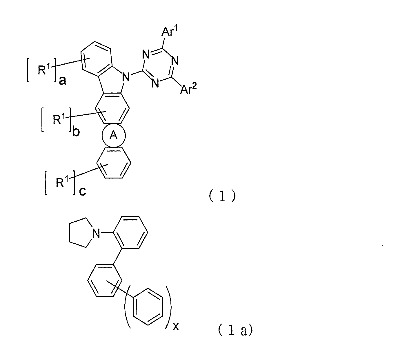
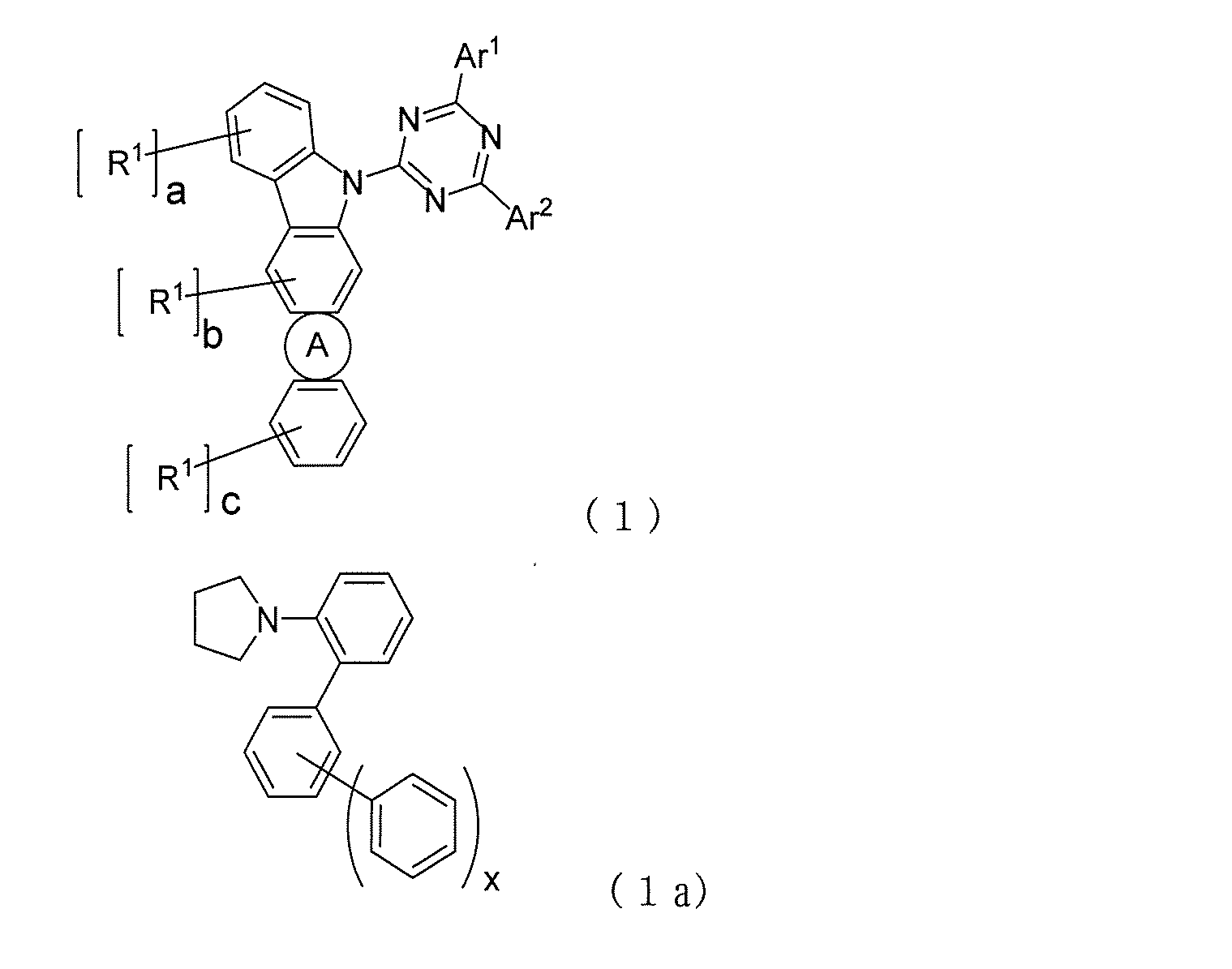
- the present invention is a mixed composition containing a compound represented by general formula (1) and a compound represented by the following general formula (2).
- ring A is a heterocycle represented by formula (1a) which is fused with two adjacent rings at any position.
- Ar 1 and Ar 2 are each independently a substituted or unsubstituted phenyl group, a substituted or unsubstituted biphenyl group, a substituted or unsubstituted terphenyl group, or a substituted or unsubstituted quaterphenyl group.
- the total number of benzene rings contained in Ar 1 and Ar 2 is preferably 2 to 6, and more preferably 2 to 4.
- R 1 's are each independently a substituted or unsubstituted aromatic hydrocarbon group having 6 to 10 carbon atoms, a substituted or unsubstituted aromatic heterocyclic group having 3 to 12 carbon atoms, or a substituted or unsubstituted linked aromatic group in which 2 to 5 of these aromatic groups are linked together, and when linked, the aromatic hydrocarbon groups or aromatic heterocyclic groups may be the same or different.
- the letters a to c represent the number of substitutions, with a and c being integers from 0 to 4 and b being an integer from 0 to 2, and preferably, a and c being integers from 0 to 2 and b being an integer from 0 to 1.
- the letter x represents the number of substitutions and is an integer from 0 to 5, preferably from 0 to 3, more preferably from 0 to 2, and even more preferably from 0 to 1. When x is from 2 to 5, it becomes a bulky substituent, suppressing interactions between molecules, and it is expected that a film with high amorphous stability can be formed.
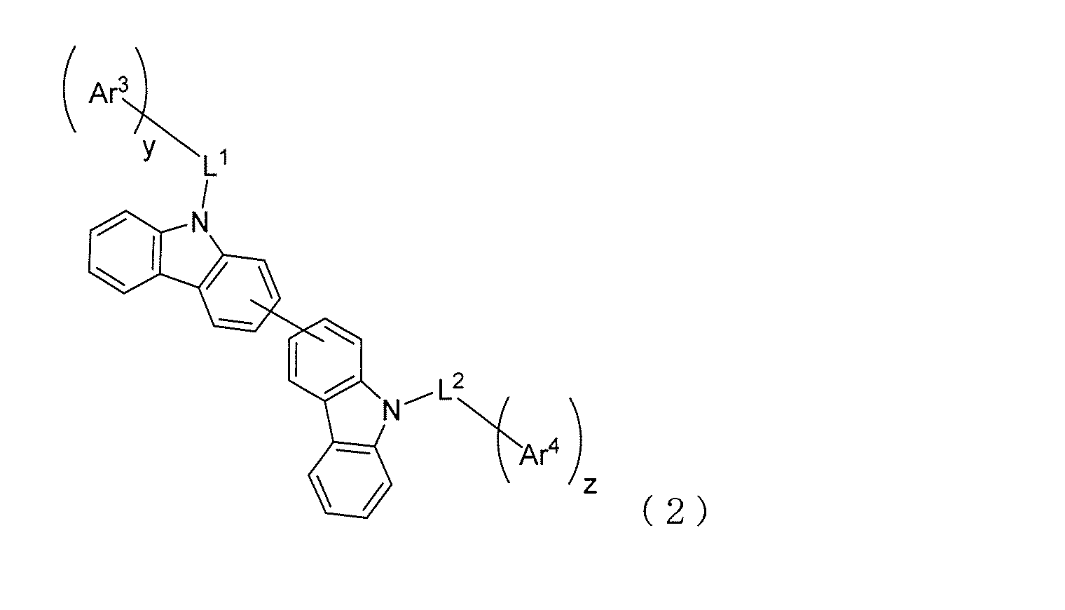
- Ar 3 and Ar 4 each independently represent a substituted or unsubstituted aromatic hydrocarbon group having 6 to 14 carbon atoms, or a substituted or unsubstituted linked aromatic group formed by linking two of these aromatic hydrocarbon groups, and when linked, the aromatic hydrocarbon groups may be the same or different.
- Ar 3 and Ar 4 are preferably a substituted or unsubstituted phenyl group, a substituted or unsubstituted biphenyl group, a substituted or unsubstituted naphthyl group, or a substituted or unsubstituted phenanthryl group, and more preferably an unsubstituted phenyl group.
- L1 and L2 each independently represent a direct bond or a substituted or unsubstituted phenylene group.
- L1 or L2 is not a direct bond, and the phenylene group is a trivalent phenylene group.
- the mixed composition preferably contains 20 wt % or more and 70 wt % or less of the compound represented by general formula (1) relative to the total of the compound represented by general formula (1) and the compound represented by general formula (2).
- At least one of the compound represented by the general formula (1) and the compound represented by the general formula (2) preferably has some or all of its hydrogen atoms substituted with deuterium atoms.
- a part or all of hydrogen is replaced with deuterium, and the average deuteration rate is preferably 30% or more, and more preferably 40% or more.
- the mixed composition is a material for producing at least one layer of an organic electroluminescent device by a vapor deposition method, and may be a premixture that is mixed in advance before vapor deposition. In this premixture, it is preferable that the difference in 50% weight loss temperature between the compound represented by the general formula (1) and the compound represented by the general formula (2) is within 20°C.
- the present invention also provides an organic electroluminescent device having multiple organic layers between an anode and a cathode, characterized in that at least one of the organic layers contains the above-mentioned mixed composition.
- the organic layer containing the mixed composition is at least one layer selected from the group consisting of a light-emitting layer, a hole injection layer, a hole transport layer, an electron transport layer, an electron injection layer, a hole blocking layer, and an electron blocking layer, and is more preferably a light-emitting layer.
- the light-emitting layer preferably contains at least one light-emitting dopant, and more preferably contains a compound represented by the general formula (1) as a first host and a compound represented by the general formula (2) as a second host, and the light-emitting layer preferably contains at least one light-emitting dopant.
- the present invention also provides a method for producing an organic electroluminescent device having a plurality of organic layers, including a light-emitting layer, between an anode and a cathode, the method comprising the steps of preparing the above-mentioned mixed composition, evaporating the mixed composition from one evaporation source, and depositing the mixture to form a light-emitting layer.
- the materials used in the organic layers have high durability against electric charges, and it is particularly important to suppress the leakage of excitons and electric charges to the surrounding layers in the light-emitting layer.
- the charge injection and transport properties of the material used in the organic layer are largely influenced by the energy level of the molecular orbital of the material and the magnitude of the intermolecular interaction.
- the mixed composition of the present invention contains an indolocarbazole compound having a biphenyldiyl group linked at the ortho position represented by formula (1a), so that the electron injection and transport properties are particularly high, but the steric hindrance effect of the biphenyldiyl group can prevent the indolocarbazole molecules from approaching each other.
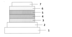
- FIG. 1 is a cross-sectional view showing an example of a structure of an organic EL element.
- the mixed composition of the present invention contains a compound represented by the general formula (1) and a compound represented by the general formula (2).
- ring A is a five-membered heterocycle represented by formula (1a), which is fused to two adjacent rings at any position, but is not fused to a side containing N. Therefore, the indolocarbazole ring has several isomeric structures, but the number is limited.
- the compound represented by general formula (1) has an embodiment represented by any one of the following formulas (3) to (8), preferably the formulas (6) to (8), and more preferably the structure represented by formula (8).
- formulas (3) to (8) symbols common to general formula (1) have the same meanings.
- Ar 1 and Ar 2 are each independently a substituted or unsubstituted phenyl group, a substituted or unsubstituted biphenyl group, a substituted or unsubstituted terphenyl group, or a substituted or unsubstituted quaterphenyl group, and the sum of the numbers of benzene rings in Ar 1 and Ar 2 is preferably 5 or less, more preferably 4 or less.
- the biphenyl group, terphenyl group, or quaterphenyl group has a structure in which 2, 3, or 4 benzene rings are linked together, and the bonding position of each benzene ring may be any of o-, m-, or p-positions. In addition, it may be linear or branched.
- R 1 's are each independently a substituted or unsubstituted aromatic hydrocarbon group having 6 to 10 carbon atoms, a substituted or unsubstituted aromatic heterocyclic group having 3 to 12 carbon atoms, or a substituted or unsubstituted linked aromatic group in which 2 to 5 of these aromatic groups are linked together, and when linked, the aromatic hydrocarbon groups or aromatic heterocyclic groups may be the same or different.
- a linking aromatic group refers to an aromatic group in which the aromatic rings of two or more aromatic groups are linked by single bonds. These linking aromatic groups may be linear or branched. The linking position when the benzene rings are linked together may be ortho, meta, or para, with para- or meta-linking being preferred.
- the aromatic group may be an aromatic hydrocarbon group or an aromatic heterocyclic group, and the multiple aromatic groups may be the same or different.
- R 1 which is an unsubstituted aromatic hydrocarbon group having 6 to 10 carbon atoms, an unsubstituted aromatic heterocyclic group having 3 to 12 carbon atoms, or an unsubstituted linked aromatic group in which 2 to 5 of these aromatic groups are linked together
- the aromatic hydrocarbon group, aromatic heterocyclic group, or linking aromatic group may each have a substituent.
- the substituent is preferably deuterium, halogen, a cyano group, a triarylsilyl group, an aliphatic hydrocarbon group having 1 to 10 carbon atoms, an alkenyl group having 2 to 5 carbon atoms, an alkoxy group having 1 to 5 carbon atoms, or a diarylamino group having 12 to 44 carbon atoms.
- the substituent is an aliphatic hydrocarbon group having 1 to 10 carbon atoms, it may be linear, branched, or cyclic.
- the triarylsilyl group or the diarylamino group is a substituent of the aromatic hydrocarbon group, aromatic heterocyclic group, or linking aromatic group, silicon and carbon, or nitrogen and carbon, are bonded by a single bond, respectively.
- the number of the above-mentioned substituents is preferably 0 to 5, and more preferably 0 to 2.
- the aromatic hydrocarbon group and aromatic heterocyclic group have a substituent, the number of carbon atoms is calculated not including the number of carbon atoms of the substituent. However, it is preferable that the total number of carbon atoms including the number of carbon atoms of the substituent falls within the above range.
- substituents include deuterium, cyano, methyl, ethyl, propyl, i-propyl, butyl, t-butyl, pentyl, neopentyl, cyclopentyl, hexyl, cyclohexyl, heptyl, octyl, nonyl, decyl, vinyl, propenyl, butenyl, pentenyl, methoxy, ethoxy, propoxy, butoxy, pentoxy, diphenylamino, naphthylphenylamino, dinaphthylamino, dianthranylamino, diphenanthrenylamino, dipyrenylamino, etc.
- the number of substitutions of n of the substituted deuterium (D) means the average number, and changes depending on the average deuteration rate.
- Ar 3 and Ar 4 each independently represent a substituted or unsubstituted aromatic hydrocarbon group having 6 to 14 carbon atoms, or a substituted or unsubstituted linked aromatic group formed by linking two of these aromatic hydrocarbon groups.
- it is a substituted or unsubstituted aromatic hydrocarbon group having 6 to 10 carbon atoms, or a substituted or unsubstituted linked aromatic group formed by linking two of these aromatic hydrocarbon groups.
- the biphenyl group has a structure in which two benzene rings are linked, and the bonding position of each benzene ring may be any of the o-, m-, and p-positions.
- specific examples of the unsubstituted aromatic hydrocarbon group having 6 to 14 carbon atoms or the unsubstituted linked aromatic group formed by linking two of these aromatic groups include groups derived from benzene, naphthalene, phenanthrene, and compounds formed by linking two of these.
- L1 and L2 each represent a direct bond or a substituted or unsubstituted phenylene group, which may be ortho-, meta-, or para-bonded.
- Each of y and z represents the number of substitutions, and independently represents 1 or 2, preferably 1.
- L1 or L2 is a trivalent phenylene group.
- the hydrogen in the compound contained in the mixed composition of the present invention may be deuterium. That is, in general formula (1), the hydrogen of the fused ring (indolocarbazole ring) containing ring A, the hydrogen of the biphenyl group or terphenyl group substituted on the indolocarbazole ring, the hydrogen of the aromatic rings of Ar 1 , Ar 2 , and R 1 , and the hydrogen of the substituents substituted on these aromatic rings may be part or all deuterium.
- the hydrogen of the two carbazole rings in the compound represented by general formula (2), the hydrogen of the aromatic rings of Ar 3 , Ar 4 , L 1 , and L 2 , and the hydrogen of the substituents of Ar 3 , Ar 4 , L 1 , and L 2 may be part or all deuterium.
- the compounds represented by general formula (1) or general formula (2) include both a single compound and a mixture of two or more compounds. That is, the compounds represented by general formula (1) or general formula (2) may be two or more compounds included in these formulas, or may be a mixture of compounds with different deuteration numbers or deuteration positions. All of the compounds contained in the mixed composition may be deuterated, or only a portion of the compounds may be deuterated.
- the compound represented by formula (1) or (2) preferably has an average deuteration rate of 30% or more, more preferably 40% or more.
- an average deuteration rate of 50% means that on average half of all hydrogen atoms are replaced with deuterium atoms.
- the average deuteration ratio can be determined by mass spectrometry or proton nuclear magnetic resonance spectroscopy. For example, when determining by proton nuclear magnetic resonance spectroscopy, a measurement sample is first prepared by adding and dissolving the compound and an internal standard in a heavy solvent, and the proton concentration [mol/g] of the compound contained in the measurement sample is calculated from the integrated intensity ratio from the internal standard and the compound. Next, the ratio of the proton concentration of the deuterated compound to the proton concentration of the corresponding non-deuterated compound is calculated, and the average deuteration ratio of the deuterated compounds can be calculated by subtracting it from 1.
- the mixed composition of the present invention contains a compound represented by the general formula (1) and a compound represented by the general formula (2), and the mixing ratio (weight ratio) is preferably such that the compound represented by the general formula (1) accounts for 20 to 70 wt %, and more preferably 20 to 60 wt %, of the total of the two.
- the mixed composition may contain other compounds in addition to the compound represented by general formula (1) and the compound represented by general formula (2).
- the other compounds may include known host materials and luminescent dopants.
- the compound represented by general formula (1) and the compound represented by general formula (2) should be 50 wt% or more of the total, and more preferably 75 wt% or more.
- the mixed composition of the present invention is suitable as a material or component of an organic EL device.
- the mixed composition is used as a component of an organic EL device, it is contained in an organic layer of the organic EL device, and this organic layer is preferably selected from the group consisting of a light-emitting layer, a hole-injection layer, a hole-transport layer, an electron-transport layer, an electron-injection layer, a hole-blocking layer, and an electron-blocking layer, and is preferably a light-emitting layer, and the light-emitting layer preferably contains at least one light-emitting dopant.
- the light-emitting layer contains the mixed composition of the present invention
- the light-emitting layer contains the mixed composition as a host.
- the compound represented by the general formula (1) is used as the first host
- the compound represented by the general formula (2) is used as the second host.
- the mixed composition of the present invention When the mixed composition of the present invention is used as a component of an organic EL device, a method of vapor-depositing a plurality of compounds such as the compound represented by the general formula (1) and the compound represented by the general formula (2) individually from different vapor deposition sources can be adopted. However, it is preferable to premix the compounds before vapor deposition to prepare a premixture, and then simultaneously evaporate and vapor-deposit the premixture from one vapor deposition source to form an organic layer, preferably a light-emitting layer. When the above premix is used as the mixed composition of the present invention to form a light-emitting layer, a necessary light-emitting dopant material or other hosts to be used as necessary may be mixed therein. However, when there is a large difference in the temperature at which the desired vapor pressure is obtained, it is preferable to deposit the light-emitting dopant material and other hosts from different deposition sources.
- the mixed composition of the present invention is the above-mentioned preliminary mixture, in order to perform stable deposition, it is desirable that the compound represented by the general formula (1) and the compound represented by the general formula (2) have a 50% weight loss temperature within 20°C. More preferably, it is within 15°C.
- the organic EL element of the present invention has a plurality of organic layers between opposing electrodes, and at least one of the organic layers is an emitting layer. At least one of the emitting layers preferably contains the mixed composition as a host. When the emitting layer contains the mixed composition, it preferably contains at least one luminescent dopant.
- FIG. 1 is a cross-sectional view showing an example of the structure of a general organic EL element used in the present invention, in which 1 is a substrate, 2 is an anode, 3 is a hole injection layer, 4 is a hole transport layer, 5 is a light-emitting layer, 6 is an electron transport layer, and 7 is a cathode.
- the organic EL element of the present invention may have an exciton blocking layer adjacent to the light-emitting layer, or an electron blocking layer between the light-emitting layer and the hole injection layer.
- the exciton blocking layer can be inserted on either the anode side or the cathode side of the light-emitting layer, or both can be inserted at the same time.
- the organic EL element of the present invention has an anode, a light-emitting layer, and a cathode as essential layers, but may have a hole injection transport layer and an electron injection transport layer in addition to the essential layers, and may further have a hole blocking layer between the light-emitting layer and the electron injection transport layer.
- the hole injection transport layer means either the hole injection layer or the hole transport layer, or both
- the electron injection transport layer means either the electron injection layer or the electron transport layer, or both.
- the organic EL element of the present invention is preferably supported by a substrate.
- a substrate There are no particular limitations on the substrate, and any substrate that has been conventionally used in organic EL elements, such as glass, transparent plastic, quartz, etc., can be used.
- anode material in the organic EL element a material consisting of a metal, alloy, electrically conductive compound, or a mixture thereof having a large work function (4 eV or more) is preferably used.
- electrode materials include metals such as Au, CuI, indium tin oxide (ITO), SnO 2 , ZnO, and other conductive transparent materials.
- amorphous materials such as IDIXO (In2O3-ZnO) that can form a transparent conductive film may be used.
- the anode may be formed by forming a thin film of these electrode materials by a method such as vapor deposition or sputtering, and forming a pattern of a desired shape by a photolithography method, or when pattern accuracy is not required very much (about 100 ⁇ m or more), a pattern may be formed through a mask of a desired shape during vapor deposition or sputtering of the electrode material.
- a coatable material such as an organic conductive compound
- a wet film formation method such as a printing method or a coating method may be used.
- the sheet resistance of the anode is preferably several hundred ⁇ / ⁇ or less.
- the film thickness depends on the material, but is usually selected from the range of 10 to 1000 nm, preferably 10 to 200 nm.
- the cathode material a material consisting of a metal (electron injecting metal), an alloy, an electrically conductive compound, or a mixture thereof having a small work function (4 eV or less) is used.
- electrode materials include sodium, sodium-potassium alloy, magnesium, lithium, a magnesium/copper mixture, a magnesium/silver mixture, a magnesium/aluminum mixture, a magnesium/indium mixture, an aluminum/aluminum oxide (Al 2 O 3 ) mixture, indium, a lithium/aluminum mixture, and a rare earth metal.
- a mixture of an electron injecting metal and a second metal having a larger and more stable work function than the electron injecting metal such as a magnesium/silver mixture, a magnesium/aluminum mixture, a magnesium/indium mixture, an aluminum/aluminum oxide mixture, a lithium/aluminum mixture, and aluminum, is preferred.
- the cathode can be produced by forming a thin film of these cathode materials by a method such as deposition or sputtering.
- the sheet resistance of the cathode is preferably several hundred ⁇ / ⁇ or less, and the film thickness is usually selected in the range of 10 nm to 5 ⁇ m, preferably 50 to 200 nm.
- the anode or the cathode of the organic EL element is transparent or semi-transparent in order to transmit the emitted light, the luminance of the emitted light is improved, which is advantageous.
- a transparent or translucent cathode can be made by forming the conductive transparent material mentioned in the explanation of the anode on top of it. By applying this, it is possible to make an element in which both the anode and cathode are optically transparent.
- the light-emitting layer is a layer that emits light after excitons are generated by recombination of holes and electrons injected from the anode and cathode, respectively, and contains a light-emitting dopant material and a host.
- the mixed composition of the present invention can be suitably used as a material for organic electroluminescent devices, and can preferably be used as a host. It is preferable to use a compound represented by general formula (1) as the first host and a compound represented by general formula (2) as the second host. One type of the first host or second host may be used, or two or more different compounds may be used. If necessary, one or more other known host materials may be used in combination, but the amount used should be 50 wt % or less, preferably 25 wt % or less, based on the total host materials.
- the method for manufacturing an organic electroluminescent device of the present invention includes the steps of preparing the above premixture, and evaporating and depositing the premixture from a single evaporation source to form a light-emitting layer.
- the method of vaporizing and depositing the premixture from a single evaporation source is more preferable.
- the 50% weight loss temperature is the temperature at which the weight is reduced by 50% when the temperature is raised from room temperature to 550°C at a rate of 10°C per minute in TG-DTA measurement under reduced pressure (1 Pa) of nitrogen gas flow. It is believed that vaporization by evaporation or sublimation occurs most actively around this temperature.
- the difference in the 50% weight loss temperature is preferably within 20°C, because a uniform deposition film can be obtained when this premix is vaporized from a single evaporation source and deposited.
- the premix may be mixed with a luminescent dopant material required to form a light-emitting layer or other hosts to be used as necessary.
- a method capable of mixing as uniformly as possible is preferable.
- the method include pulverization and mixing, a method of heating and melting the materials under reduced pressure or in an inert gas atmosphere such as nitrogen, and sublimation, but the method is not limited to these.
- the premix may be in the form of a powder, stick, or granules.
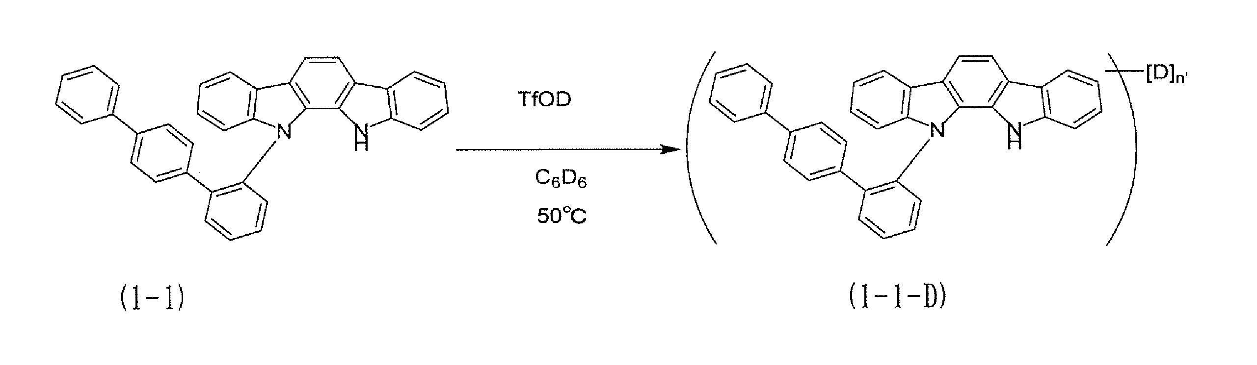
- known methods include a method of producing the compound using a fully or partially deuterated starting material, and a method of producing the compound by a hydrogen/deuterium exchange reaction.
- the fully or partially deuterated starting material can be purchased from a commercial source or produced by a known hydrogen/deuterium exchange reaction.
- Known hydrogen/deuterium exchange reactions include a method in which a non-deuterated product is subjected to deuterium gas or its equivalent in the presence of a transition metal catalyst, and a method in which a non-deuterated product is treated with a deuterated solvent (such as deuterated benzene) in the presence of an acid catalyst.
- the phosphorescent dopant when used as the luminescent dopant material, the phosphorescent dopant preferably contains an organometallic complex containing at least one metal selected from ruthenium, rhodium, palladium, silver, rhenium, osmium, iridium, platinum, and gold.
- the iridium complexes described in J.Am.Chem.Soc.2001,123,4304, JP2013-530515A, US2016/0049599A, US2017/0069848A, US2018/0282356A, or US2019/0036043A, or the platinum complexes described in US2018/0013078A or KR2018-094482A, are preferably used, but are not limited to these.
- the light-emitting layer may contain only one type of phosphorescent dopant material, or may contain two or more types.
- the content of the phosphorescent dopant material is preferably 0.1 to 30 wt % relative to the host material, and more preferably 1 to 20 wt %.
- Phosphorescent dopant materials are not particularly limited, but specific examples include the following compounds:
- fluorescent dopant examples include, but are not limited to, benzoxazole derivatives, benzothiazole derivatives, benzimidazole derivatives, styrylbenzene derivatives, polyphenyl derivatives, diphenylbutadiene derivatives, tetraphenylbutadiene derivatives, naphthalimide derivatives, coumarin derivatives, condensed aromatic compounds, perinone derivatives, oxadiazole derivatives, oxazine derivatives, aldazine derivatives, pyrrolidine derivatives, cyclopentadiene derivatives, bisstyrylanthracene derivatives, quinacridone derivatives, pyrrolopyridine derivatives, thiadiazolopyridine derivatives, styrylamine derivatives, diketopyrrolopyrrole derivatives, aromatic dimethylidine compounds, various metal complexes such as metal complexes of 8-quinol
- thermally activated delayed fluorescent dopant When a thermally activated delayed fluorescent dopant is used as the luminescent dopant material, examples of the thermally activated delayed fluorescent dopant include, but are not limited to, metal complexes such as tin complexes and copper complexes, indolocarbazole derivatives described in WO2011/070963A, cyanobenzene derivatives and carbazole derivatives described in Nature 2012,492,234, phenazine derivatives, oxadiazole derivatives, triazole derivatives, sulfone derivatives, phenoxazine derivatives and acridine derivatives described in Nature Photonics 2014,8,326, etc.
- metal complexes such as tin complexes and copper complexes
- indolocarbazole derivatives described in WO2011/070963A cyanobenzene derivatives and carbazole derivatives described in Nature 2012,492,234, phenazine derivatives, oxadiazole derivatives
- the thermally activated delayed fluorescent dopant material is not particularly limited, but specific examples thereof include the following compounds.
- the light-emitting layer may contain only one type of thermally activated delayed fluorescent dopant material, or may contain two or more types.
- the thermally activated delayed fluorescent dopant may be mixed with a phosphorescent dopant or a fluorescent dopant.
- the content of the thermally activated delayed fluorescent dopant material is preferably 0.1 to 50 wt %, and more preferably 1 to 30 wt %, relative to the host material.
- the injection layer is a layer provided between an electrode and an organic layer to reduce the driving voltage and improve the luminance of light emitted, and includes a hole injection layer and an electron injection layer, and may be provided between the anode and the light emitting layer or the hole transport layer, and between the cathode and the light emitting layer or the electron transport layer.
- the injection layer can be provided as necessary.
- a hole blocking layer in a broad sense, has the function of an electron transport layer and is made of a hole blocking material that has the function of transporting electrons but has an extremely low ability to transport holes, and by transporting electrons while blocking holes, it is possible to improve the probability of recombination of electrons and holes in the light-emitting layer.
- the electron blocking layer functions as a hole transport layer, and can increase the probability of recombination of electrons and holes in the light emitting layer by blocking electrons while transporting holes.
- the electron blocking layer may be made of a known material, or may be made of a material for the hole transport layer, as described below, if necessary.
- the thickness of the electron blocking layer is preferably 3 to 100 nm, and more preferably 5 to 30 nm.
- the exciton blocking layer is a layer for preventing excitons generated by the recombination of holes and electrons in the light-emitting layer from diffusing into the charge transport layer, and the insertion of this layer makes it possible to efficiently confine excitons in the light-emitting layer, thereby improving the luminous efficiency of the device.
- the exciton blocking layer can be inserted between two adjacent light-emitting layers.
- the material for the exciton blocking layer can be any known exciton blocking layer material. Examples include 1,3-dicarbazolylbenzene (mCP) and bis(8-hydroxy-2-methylquinoline)-(4-phenylphenoxy)aluminum(III) (BAlq).
- mCP 1,3-dicarbazolylbenzene
- BAlq bis(8-hydroxy-2-methylquinoline)-(4-phenylphenoxy)aluminum(III)
- the hole transport layer is made of a hole transport material having a function of transporting holes, and the hole transport layer may be provided as a single layer or multiple layers.
- the hole transport material is one that has either hole injection or transport properties or electron barrier properties, and may be either organic or inorganic. Any of the conventionally known compounds may be selected and used for the hole transport layer. Examples of such hole transport materials include porphyrin derivatives, arylamine derivatives, triazole derivatives, oxadiazole derivatives, imidazole derivatives, polyarylalkane derivatives, pyrazoline derivatives and pyrazolone derivatives, phenylenediamine derivatives, arylamine derivatives, amino-substituted chalcone derivatives, oxazole derivatives, styrylanthracene derivatives, fluorenone derivatives, hydrazone derivatives, stilbene derivatives, silazane derivatives, aniline-based copolymers, and conductive polymer oligomers, particularly thiophene oligomers, etc., but it is preferable to use porphyrin derivatives, arylamine derivatives, and styrylamine derivative
- the electron transport layer is made of a material having a function of transporting electrons, and the electron transport layer may be provided as a single layer or as a multi-layer.
- the electron transport material (which may also serve as a hole blocking material) may have the function of transmitting electrons injected from the cathode to the light emitting layer.
- any of the conventionally known compounds may be selected and used, such as polycyclic aromatic derivatives such as naphthalene, anthracene, and phenanthroline, tris(8-hydroxyquinoline)aluminum(III) derivatives, phosphine oxide derivatives, nitro-substituted fluorene derivatives, diphenylquinone derivatives, thiopyran dioxide derivatives, carbodiimides, fluorenylidenemethane derivatives, anthraquinodimethane and anthrone derivatives, bipyridine derivatives, quinoline derivatives, oxadiazole derivatives, benzimidazole derivatives, benzothiazole derivatives, and indolocarbazole derivatives.
- polymeric materials in which these materials are introduced into the polymer chain or in which
- the average deuteration rate of compound 705 was determined by proton nuclear magnetic resonance spectroscopy.
- a measurement sample was prepared by dissolving compound 405 (5.0 mg) and dimethyl sulfone (2.0 mg) as an internal standard in deuterated tetrahydrofuran (1.0 ml).
- the average proton concentration [mol/g] of compound 705 contained in the measurement sample was calculated from the integrated intensity ratio from the internal standard and compound 705.
- the average proton concentration [mol/g] of the non-deuterated form of compound 705 (compound 608) was also calculated in the same manner. Next, the ratio of the proton concentration of compound 705 to the proton concentration of compound 608 was calculated, and the average deuteration rate of compound 705 was calculated to be 68.8% by subtracting it from 1.
- the average deuteration rate of compound 306 was determined by proton nuclear magnetic resonance spectroscopy.
- a measurement sample was prepared by dissolving compound 218 (5.0 mg) and dimethyl sulfone (2.0 mg) as an internal standard in deuterated tetrahydrofuran (1.0 ml).
- the average proton concentration [mol/g] of compound 306 contained in the measurement sample was calculated from the integrated intensity ratio of the internal standard and compound 306.
- the average proton concentration [mol/g] of the non-deuterated form of compound 306 (compound 114) was also calculated in the same manner.
- the ratio of the proton concentration of compound 306 to the proton concentration of compound 114 was calculated, and the average deuteration rate of compound 306 was calculated to be 53.4% by subtracting it from 1.
- Synthesis Example 4 Deuterated compounds 701, 707, 301, 309, 310, 331, and 340 were synthesized by carrying out reactions similar to those in Synthesis Examples 2 and 3. The average deuteration rates of these compounds were calculated in the same manner as for 705 and 306, and the results are shown in Table 1.
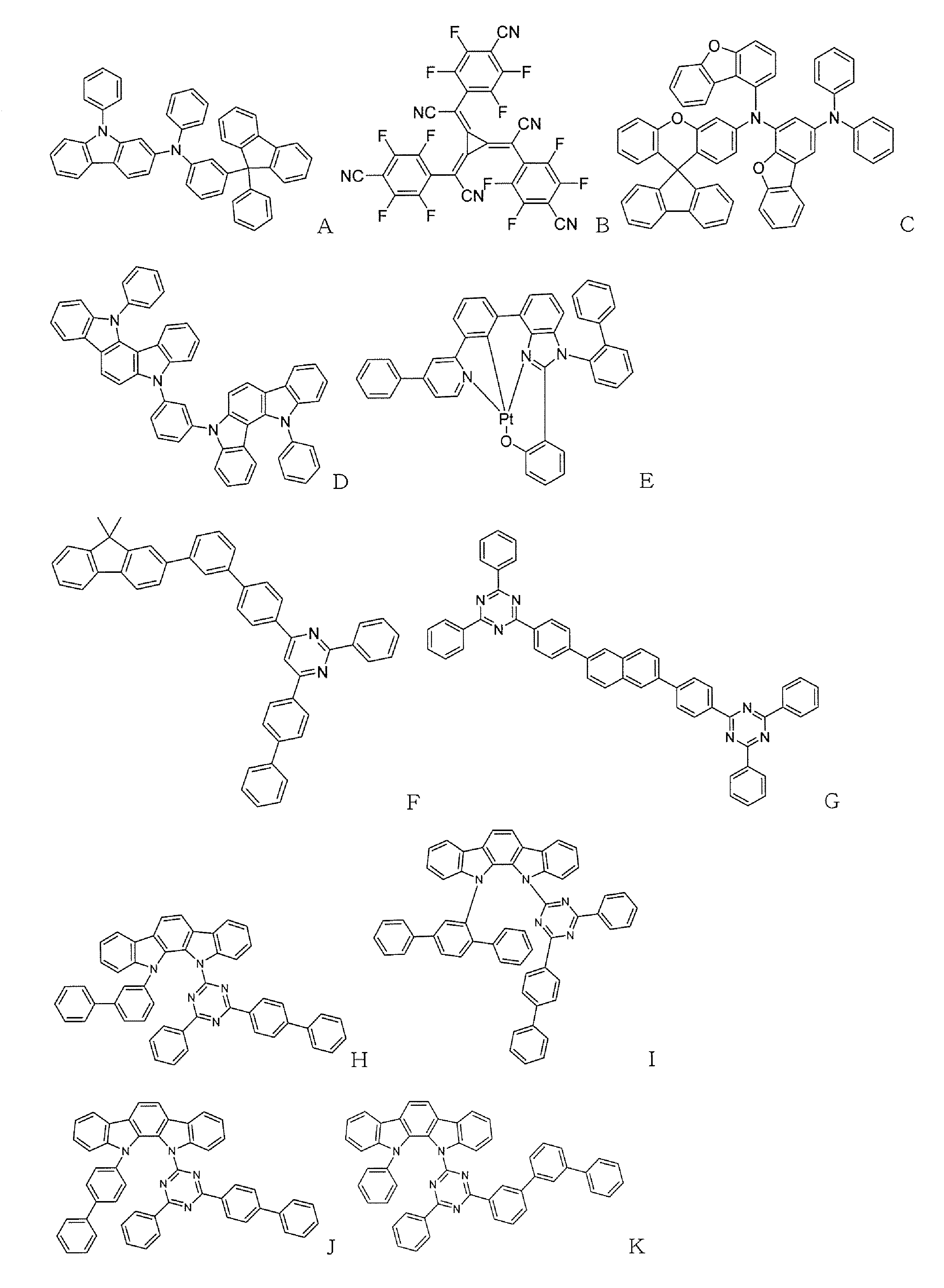
- Example 1 Each thin film was laminated by vacuum deposition at a vacuum degree of 4.0 ⁇ 10 ⁇ 5 Pa on a glass substrate on which an anode made of ITO with a thickness of 110 nm had been formed.
- compound A and compound B were co-deposited from different deposition sources on ITO to form a hole injection layer with a thickness of 10 nm. At this time, the co-deposition was performed under deposition conditions such that the concentration of compound B was 3 wt %.
- compound A was formed as a first hole transport layer to a thickness of 110 nm.
- compound C was formed as a second hole transport layer to a thickness of 10 nm.
- compound D was formed to a thickness of 5 nm as an electron blocking layer.
- a preliminary mixture of Compound 114 (first host) and Compound 608 (second host) was evaporated from a single evaporation source as a host, and Compound E was evaporated from a different evaporation source as a light-emitting dopant, and co-evaporated to form a light-emitting layer with a thickness of 40 nm.
- co-evaporation was performed under the evaporation conditions of a concentration of Compound E of 15 wt % and a weight ratio of the first host to the second host of 50:50.
- compound F was formed to a thickness of 5 nm as a hole blocking layer.
- compound G was formed as an electron transport layer to a thickness of 30 nm.
- LiF was formed as an electron injection layer to a thickness of 1 nm on the electron transport layer.
- an Al film was formed as a cathode with a thickness of 70 nm on the electron injection layer to complete an organic EL device.
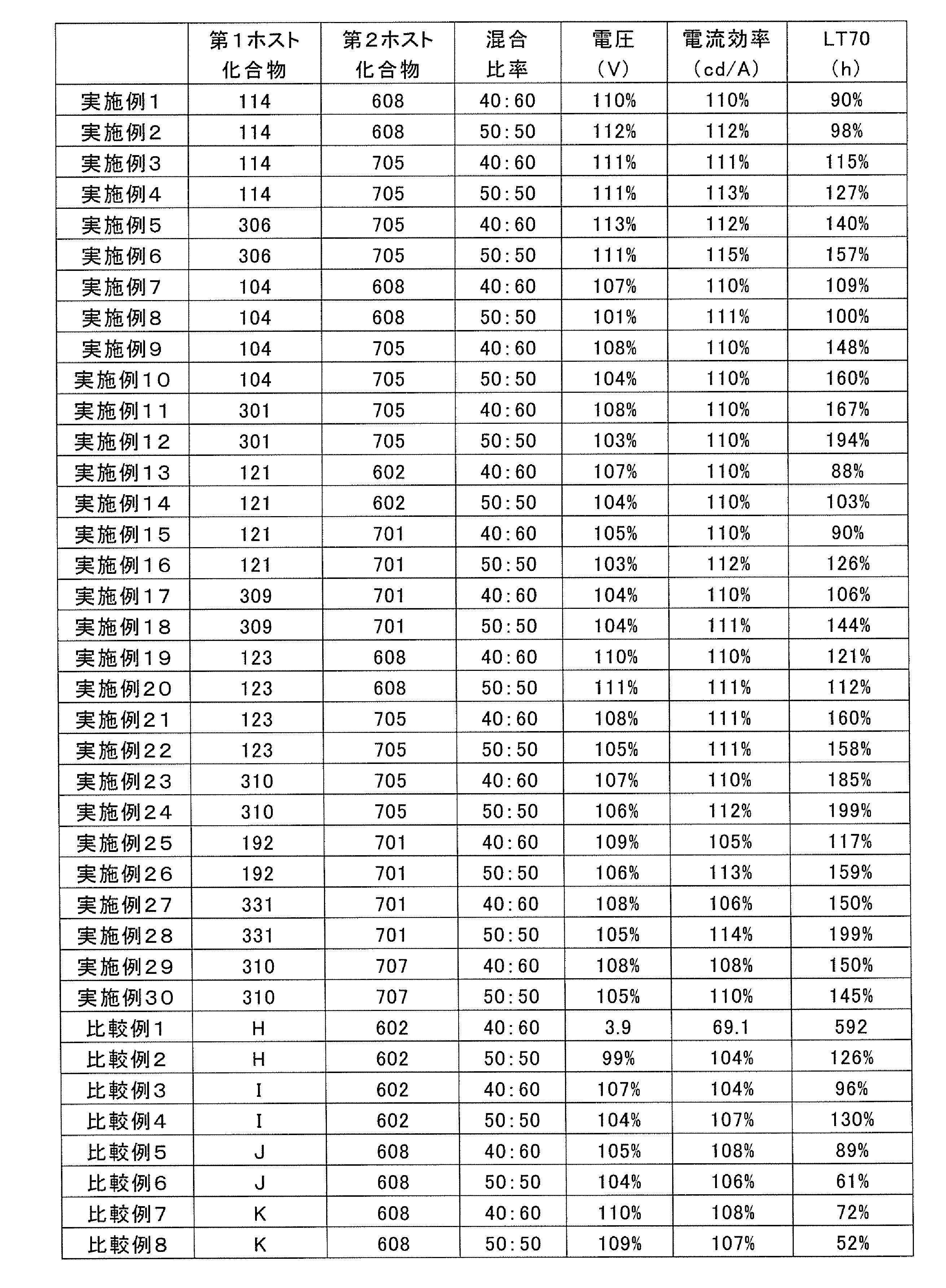
- Examples 2 to 30, Comparative Examples 1 to 8 An organic EL device was prepared in the same manner as in Example 1, except that the compounds shown in Table 2 were used as the first host and the second host in the weight ratio shown in Table 2.
- the evaluation results of the prepared organic EL device are shown in Table 2.
- the luminance, voltage, and current efficiency are values at a driving current of 10 mA/ cm2 , which are initial characteristics.
- LT70 is the time required for the luminance to decay to 70% when driven at an initial luminance of 9000 nits, and represents the life characteristics.
- the numbers of the first host and the second host are the numbers given to the above exemplary compounds, and the weight ratio is first host:second host. All characteristics are expressed as relative values with the characteristics of Comparative Example 1 taken as 100%.
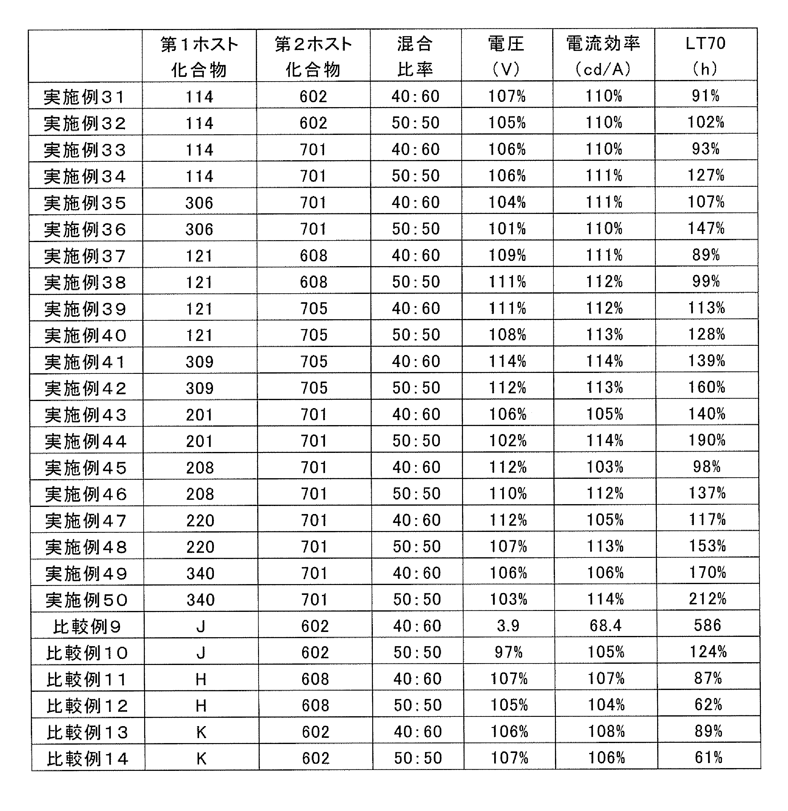
- Examples 31 to 50, Comparative Examples 9 to 14 An organic EL device was prepared in the same manner as in Example 1, except that the compounds shown in Table 3 were used as the first host and the second host and were co-deposited from different deposition sources in the weight ratio shown in Table 3.
- Examples 1 to 50 show improved efficiency and good characteristics while maintaining the same life characteristics as the comparative examples.
- efficiency and life may be in a trade-off relationship, and it is difficult to improve both current efficiency and life characteristics.
- improving current efficiency leads to lower power consumption and improved luminance, so if current efficiency can be improved while maintaining a certain level of life characteristics, a more practical element can be obtained.
- Examples 1 to 50 which use the mixed composition of the present invention, can achieve a current efficiency of 110% or more while maintaining a life characteristic of about 90% or exhibiting a life characteristic of 100% or more compared to Comparative Examples 1 and 9, in which a conventional compound was used as part of the mixed host material, and an organic EL element that is advantageous for practical use can be obtained.
- Table 4 lists the 50% weight loss temperatures (T50) for compounds 104, 114, 121, 123, 301, 309, 310, 318, 602, 608, 701, 705, 707, 192, 331, 201, 340, 208, 220, H, I, J, and K.
Landscapes
- Physics & Mathematics (AREA)
- Optics & Photonics (AREA)
- Chemical & Material Sciences (AREA)
- Engineering & Computer Science (AREA)
- Materials Engineering (AREA)
- Spectroscopy & Molecular Physics (AREA)
- Organic Chemistry (AREA)
- Manufacturing & Machinery (AREA)
- Electroluminescent Light Sources (AREA)
Abstract
Description
しかしながら、燐光発光型の有機EL素子に関しては、長寿命化が技術的な課題となっている。
一方で特許文献2では、TADF(Thermally Activated Delayed Fluorescence)機構を利用した有機EL素子が開示されている。TADF機構は一重項準位と三重項準位のエネルギー差が小さい材料において三重項励起子から一重項励起子への逆項間交差が生じる現象を利用するものであり、理論上内部量子効率を100%まで高められると考えられている。しかしながら燐光発光型素子と同様に寿命特性の更なる改善が求められている。

また、前記一般式(1)又は一般式(2)で表される化合物において、水素の一部若しくは全部が重水素で置換されており、その平均重水素化率が30%以上であることが好ましい、40%以上がより好ましい。
この予備混合物にあっては、前記一般式(1)で表される化合物と、一般式(2)で表される化合物との50%重量減少温度の差が20℃以内であるのがよい。
有機層に使用する材料の両電荷注入輸送性は、材料の分子軌道のエネルギー準位および分子間の相互作用の大きさにより大きく左右される。本発明の混合組成物を有機EL素子用材料として使用した場合は、式(1a)で表されるオルト位連結のビフェニルジイル基を有するインドロカルバゾール化合物を含むため、特に電子注入輸送能が高いが、ビフェニルジイル基の立体障害効果からインドロカルバゾール分子同士の近接を抑えることができる。
そして、ビフェニルジイル基の置換基種や結合位置を変えることで発光層への電子注入輸送への寄与の大きな分子軌道の分子間相互作用を高いレベルで制御でき、優れた有機EL素子を与えると考えられる。

なお、上記置換基の数は0~5であるのがよく、好ましくは0~2がよい。また、芳香族炭化水素基及び芳香族複素環基が置換基を有する場合の炭素数の計算には、置換基の炭素数を含まない。しかし、置換基の炭素数を含んだ合計の炭素数が上記範囲を満足することが好ましい。








y及びzは、置換数を示し、独立に1又は2を示すが、好ましくは1である。2である場合はL1又はL2は、3価のフェニレン基である。
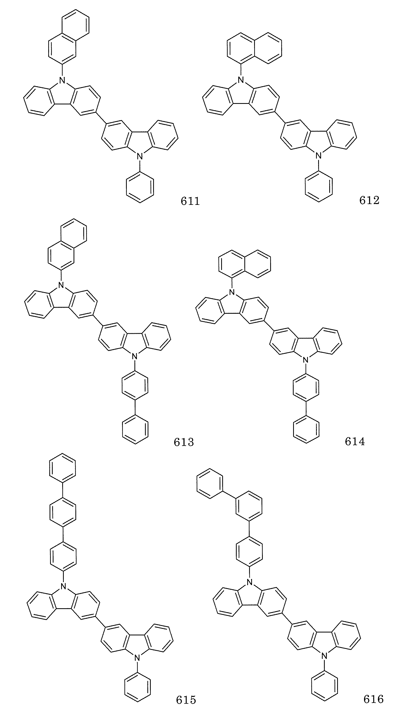


また、混合組成物中に含まれる化合物の全部が重水素化されてもよく、一部の化合物だけが重水素化されてもよい。
ここで、平均重水素化率を具体的に説明すると、平均重水素化率が50%の場合、全水素のうち平均で半数が重水素に置換されたものを意味する。
有機EL素子の成分となる場合は、混合組成物は、有機EL素子の有機層に含まれるが、この有機層としては、発光層、正孔注入層、正孔輸送層、電子輸送層、電子注入層、正孔阻止層及び電子阻止層からなる群から選ばれることがよい。好ましくは、発光層であり、発光層は少なくとも1種の発光性ドーパントを含有することがよい。
本発明の混合組成物として、上記予備混合物を使用して発光層を形成する場合は、必要な発光性ドーパント材料又は必要により使用される他のホストを混合させてもよいが、所望の蒸気圧となる温度に大きな差がある場合は、発光性ドーパント材料や他のホストは別の蒸着源から蒸着させることがよい。
本発明の有機EL素子は、基板に支持されていることが好ましい。この基板については特に制限はなく、従来から有機EL素子に用いられているものであればよく、例えばガラス、透明プラスチック、石英等からなるものを用いることができる。
有機EL素子における陽極材料としては、仕事関数の大きい(4eV以上)金属、合金、電気伝導性化合物又はこれらの混合物からなる材料が好ましく用いられる。このような電極材料の具体例としてはAu等の金属、CuI、インジウムチンオキシド(ITO)、SnO2、ZnO等の導電性透明材料が挙げられる。また、IDIXO(In2O3-ZnO)等の非晶質で、透明導電膜を作成可能な材料を用いてもよい。陽極はこれらの電極材料を蒸着やスパッタリング等の方法により、薄膜を形成させ、フォトリソグラフィー法で所望の形状のパターンを形成してもよく、あるいはパターン精度をあまり必要としない場合(100μm以上程度)は、上記電極材料の蒸着やスパッタリング時に所望の形状のマスクを介してパターンを形成してもよい。あるいは有機導電性化合物のような塗布可能な物質を用いる場合には印刷方式、コーティング方式等湿式成膜法を用いることもできる。この陽極より発光を取り出す場合には、透過率を10%より大きくすることが望ましく、また陽極としてのシート抵抗は数百Ω/□以下が好ましい。膜厚は材料にもよるが、通常10~1000nm、好ましくは10~200nmの範囲で選ばれる。
陰極材料としては、仕事関数の小さい(4eV以下)金属(電子注入性金属)、合金、電気伝導性化合物又はこれらの混合物からなる材料が用いられる。このような電極材料の具体例としては、ナトリウム、ナトリウム―カリウム合金、マグネシウム、リチウム、マグネシウム/銅混合物、マグネシウム/銀混合物、マグネシウム/アルミニウム混合物、マグネシウム/インジウム混合物、アルミニウム/酸化アルミニウム(Al2O3)混合物、インジウム、リチウム/アルミニウム混合物、希土類金属等が挙げられる。これらの中で、電子注入性及び酸化等に対する耐久性の点から、電子注入性金属とこれより仕事関数の値が大きく安定な金属である第二金属との混合物、例えばマグネシウム/銀混合物、マグネシウム/アルミニウム混合物、マグネシウム/インジウム混合物、アルミニウム/酸化アルミニウム混合物、リチウム/アルミニウム混合物、アルミニウム等が好適である。陰極はこれらの陰極材料を蒸着やスパッタリング等の方法により薄膜を形成させることにより、作製することができる。また、陰極としてシート抵抗は数百Ω/□以下が好ましく、膜厚は通常10nm~5μm、好ましくは50~200nmの範囲で選ばれる。なお、発光した光を透過させるため、有機EL素子の陽極又は陰極のいずれか一方が透明又は半透明であれば発光輝度は向上し、好都合である。
発光層は陽極及び陰極のそれぞれから注入された正孔及び電子が再結合することにより励起子が生成した後、発光する層であり発光層には発光性ドーパント材料とホストを含む。
予備混合物の形態は粉体、スティック状、又は顆粒状であってもよい。
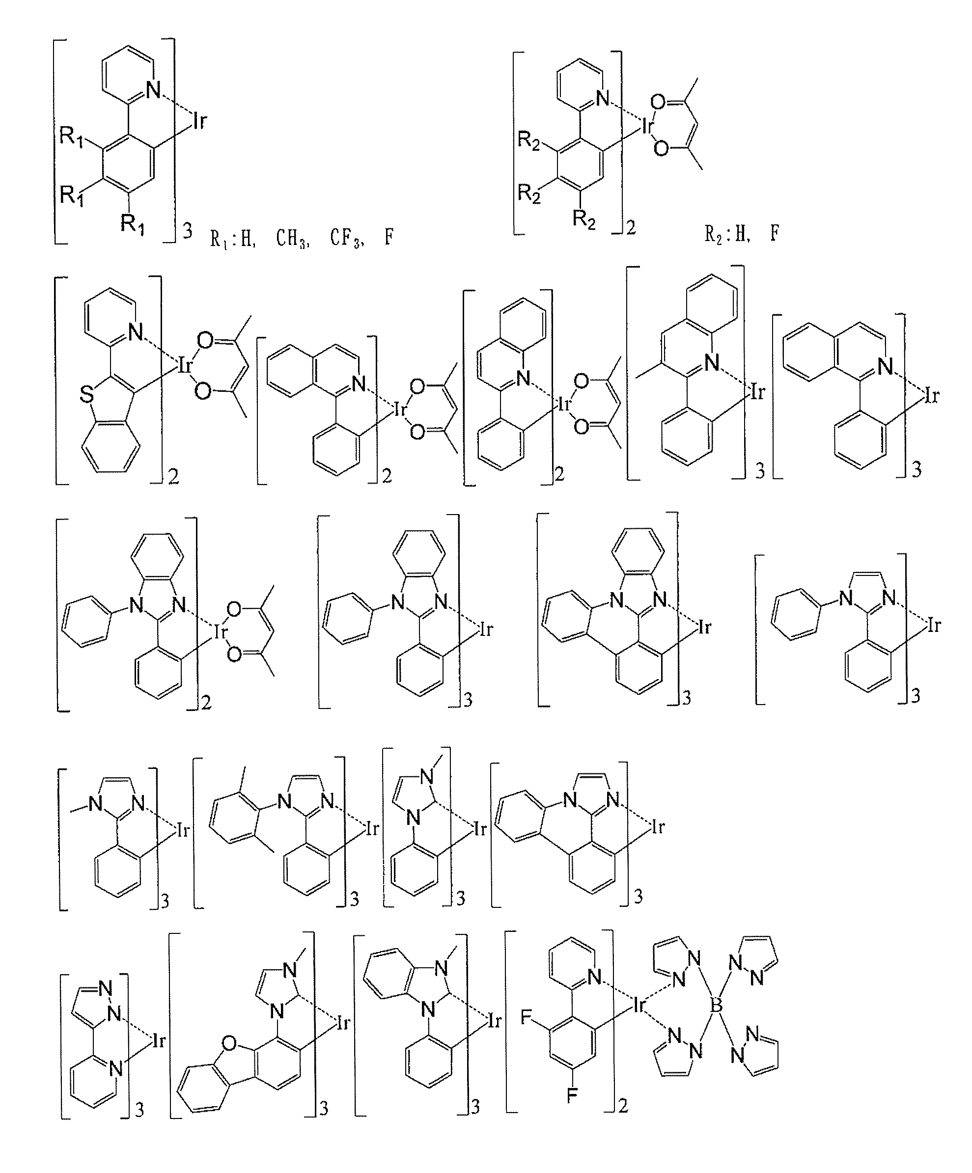

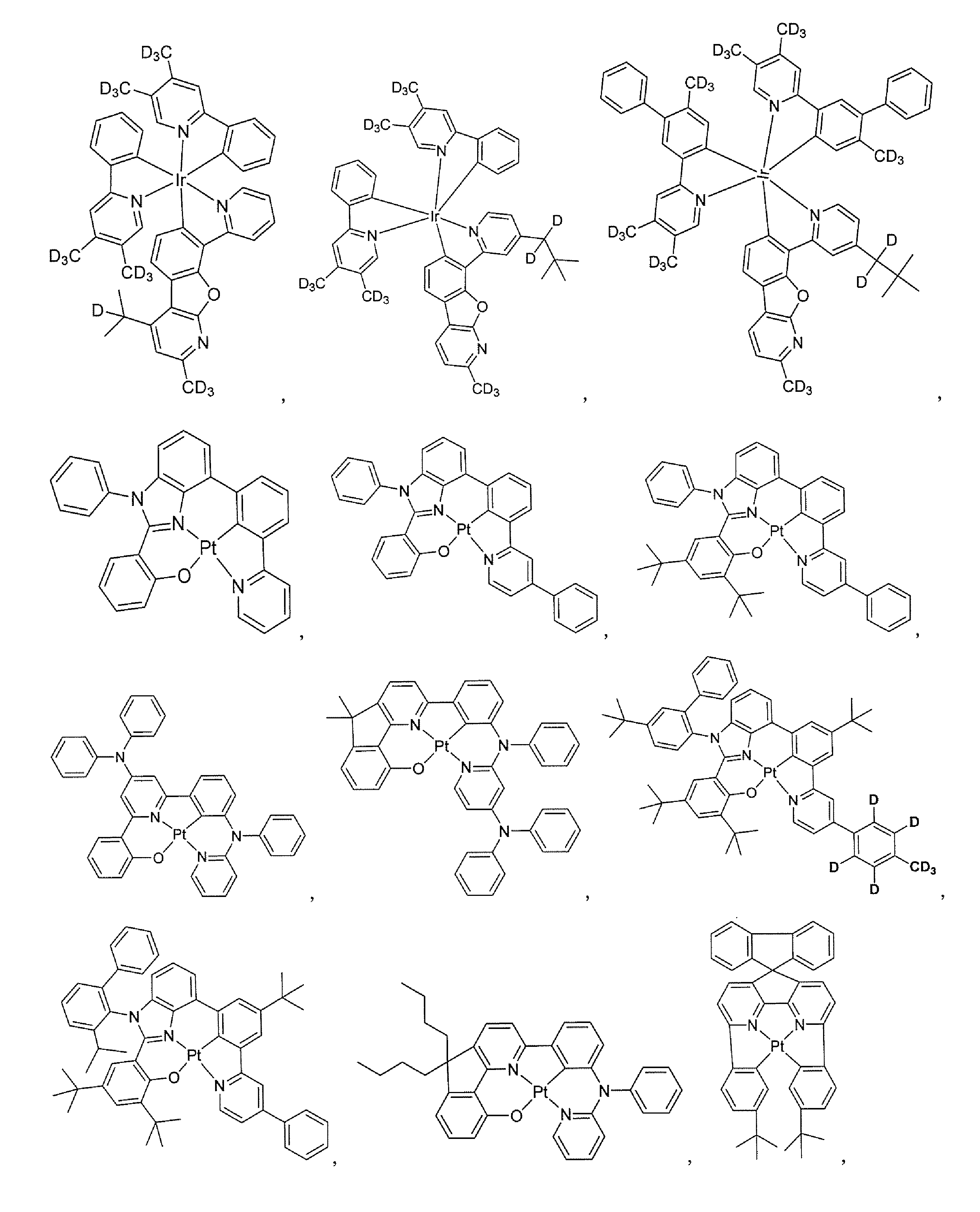

注入層とは、駆動電圧低下や発光輝度向上のために電極と有機層間に設けられる層のことで、正孔注入層と電子注入層があり、陽極と発光層又は正孔輸送層の間、及び陰極と発光層又は電子輸送層との間に存在させてもよい。注入層は必要に応じて設けることができる。
正孔阻止層とは広い意味では電子輸送層の機能を有し、電子を輸送する機能を有しつつ正孔を輸送する能力が著しく小さい正孔阻止材料からなり、電子を輸送しつつ正孔を阻止することで発光層中での電子と正孔の再結合確率を向上させることができる。
電子阻止層とは広い意味では正孔輸送層の機能を有し、正孔を輸送しつつ電子を阻止することで発光層中での電子と正孔が再結合する確率を向上させることができる。
励起子阻止層とは、発光層内で正孔と電子が再結合することにより生じた励起子が電荷輸送層に拡散することを阻止するための層であり、本層の挿入により励起子を効率的に発光層内に閉じ込めることが可能となり、素子の発光効率を向上させることができる。励起子阻止層は2つ以上の発光層が隣接する素子において、隣接する2つの発光層の間に挿入することができる。
正孔輸送層とは正孔を輸送する機能を有する正孔輸送材料からなり、正孔輸送層は単層又は複数層設けることができる。
電子輸送層とは電子を輸送する機能を有する材料からなり、電子輸送層は単層又は複数層設けることができる。

窒素雰囲気下、N,N’-ジメチルアセトアミド30mlに60重量%水素化ナトリウム1.3gを加え、懸濁液を調製した。そこにN,N’-ジメチルアセトアミド170mLに溶解した中間体(1-1)を6g加え、30分撹拌した。そこに化合物(c)を5.1g加えた後、6時間撹拌した。反応溶液をメタノール (300 ml)、蒸留水(100 ml)の混合溶液に撹拌しながら加え、得られた析出した固体をろ取した。得られた固体をシリカゲルカラムクロマトグラフィーで精製、晶析精製を行い、黄色固体として化合物114を6.5g (収率66%)得た(APCI-TOFMS、m/z 792[M+H]+)。
次の反応に従い、化合物405を合成した。


合成例2~3と同様にして反応を行い、重水素化物である化合物701、707、301、309、310、331、340を合成した。また、705及び306と同様にこれらの平均重水素化率を計算した結果を、表1に示す。

膜厚110nmのITOからなる陽極が形成されたガラス基板上に、各薄膜を真空蒸着法にて、真空度4.0×10⁻⁵Paで積層した。
先ず、ITO上に正孔注入層として化合物Aと化合物Bをそれぞれ異なる蒸着源から共蒸着し、10nmの厚さに形成した。この時化合物Bの濃度が3wt%となる蒸着条件で共蒸着した。
次に、第1正孔輸送層として化合物Aを110nmの厚さに形成した。
次に、第2正孔輸送層として化合物Cを10nmの厚さに形成した。
次に、電子阻止層として化合物Dを5nmの厚さに形成した。
次に、ホストとして化合物114(第1ホスト)と化合物608(第2ホスト)の予備混合物を単一の蒸発源から蒸発させ、発光ドーパントとして化合物Eを異なる蒸着源から蒸発させ、共蒸着し、40nmの厚さに発光層を形成した。この時、化合物Eの濃度が15wt%、第1ホストと第2ホストの重量比が50:50となる蒸着条件で共蒸着した。
次に、正孔阻止層として化合物Fを5nmの厚さに形成した。
次に、電子輸送層として化合物Gを30nmの厚さに形成した。
更に、電子輸送層上に電子注入層としてLiFを1nmの厚さに形成した。
最後に、電子注入層上に、陰極としてAlを70nmの厚さに形成し、有機EL素子を作製した。
第1ホスト及び第2ホストとして、表2示す化合物を使用し、表2に示す重量比とした以外は実施例1と同様にして有機EL素子を作製した。
第1ホスト及び第2ホストとして、表3示す化合物を使用し、表3に示す重量比でそれぞれ異なる蒸着源から共蒸着した以外は、実施例1と同様にして有機EL素子を作製した。
得られた有機EL素子について、先の実施例1等と同様にして評価した。結果を表3に示す。なお、いずれの特性も、比較例9の特性を100%とした相対値で表記してある。

Claims (14)
- 下記一般式(1)で表される化合物と、下記一般式(2)で表される化合物とを含む混合組成物。
- 前記一般式(1)で示される化合物と、前記一般式(2)で表される化合物との合計に対して、一般式(1)で表される化合物が20wt%以上70wt%以下であることを特徴とする請求項1に記載の混合組成物。
- 前記一般式(1)及び一般式(2)で表される化合物の少なくとも一方の化合物が、水素の一部若しくは全部が重水素で置換されている請求項1に記載の混合組成物。
- 前記一般式(2)で表される化合物において、水素の一部若しくは全部が重水素で置換されており、その平均重水素化率が30%以上である請求項1に記載の混合組成物。
-
混合組成物が、有機電界発光素子の少なくとも1層を蒸着法によって製造するための材料であって、蒸着前に事前に混合された予備混合物であることを特徴とする請求項1に記載の混合組成物。 - 前記一般式(1)で表される化合物と、前記一般式(2)で表される化合物との50%重量減少温度の差が20℃以内であることを特徴とする請求項5に記載の混合組成物。
- 陽極と陰極との間に複数の有機層を有する有機電界発光素子であって、該有機層の少なくとも1層に、請求項1~6のいずれかに記載の混合組成物を含むことを特徴とする有機電界発光素子。
- 前記混合組成物を含む有機層が、発光層、正孔注入層、正孔輸送層、電子輸送層、電子注入層、正孔阻止層及び電子阻止層からなる群から選ばれる少なくとも一つの層である請求項7に記載の有機電界発光素子。
- 前記混合組成物を含む有機層が発光層であり、第1ホストとして前記一般式(1)で表される化合物、及び第2ホストとして前記一般式(2)で表される化合物を含み、かつ該発光層が少なくとも1種の発光性ドーパントを含有する請求項7に記載の有機電界発光素子。
- 陽極と陰極との間に発光層を含む複数の有機層を有する有機電界発光素子を製造する方法であって、請求項5に記載の混合組成物を用意すること、この混合組成物を一つの蒸発源から蒸発させ、蒸着させて発光層を形成することからなる工程を有することを特徴とする有機電界発光素子の製造方法。
- 前記一般式(1)で表される化合物において、置換数xが0~2の整数である、請求項1に記載の混合組成物。
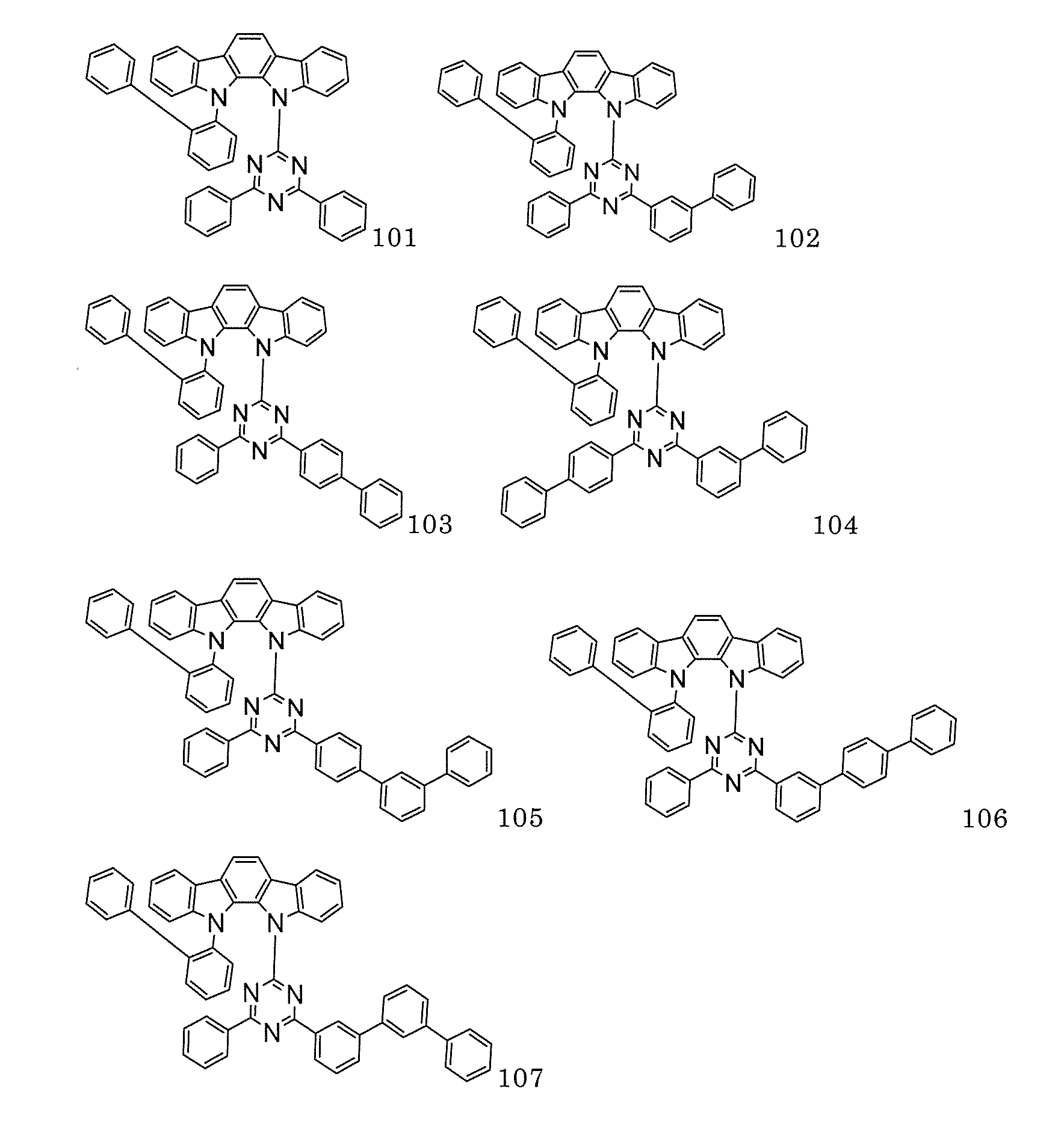
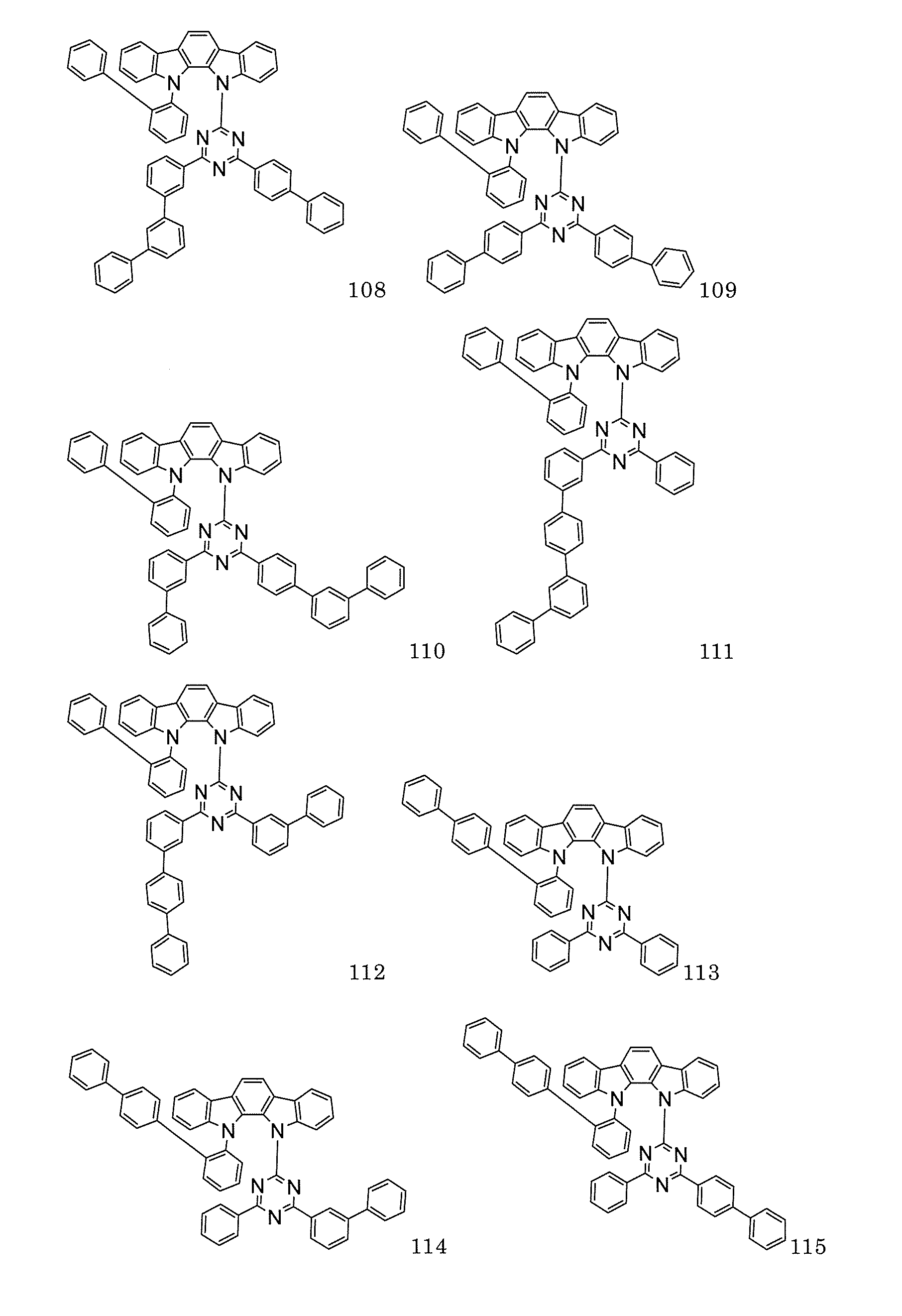
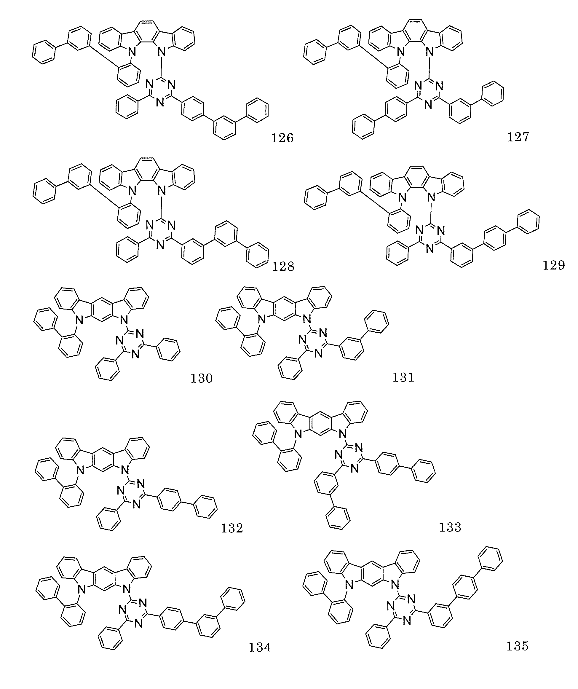
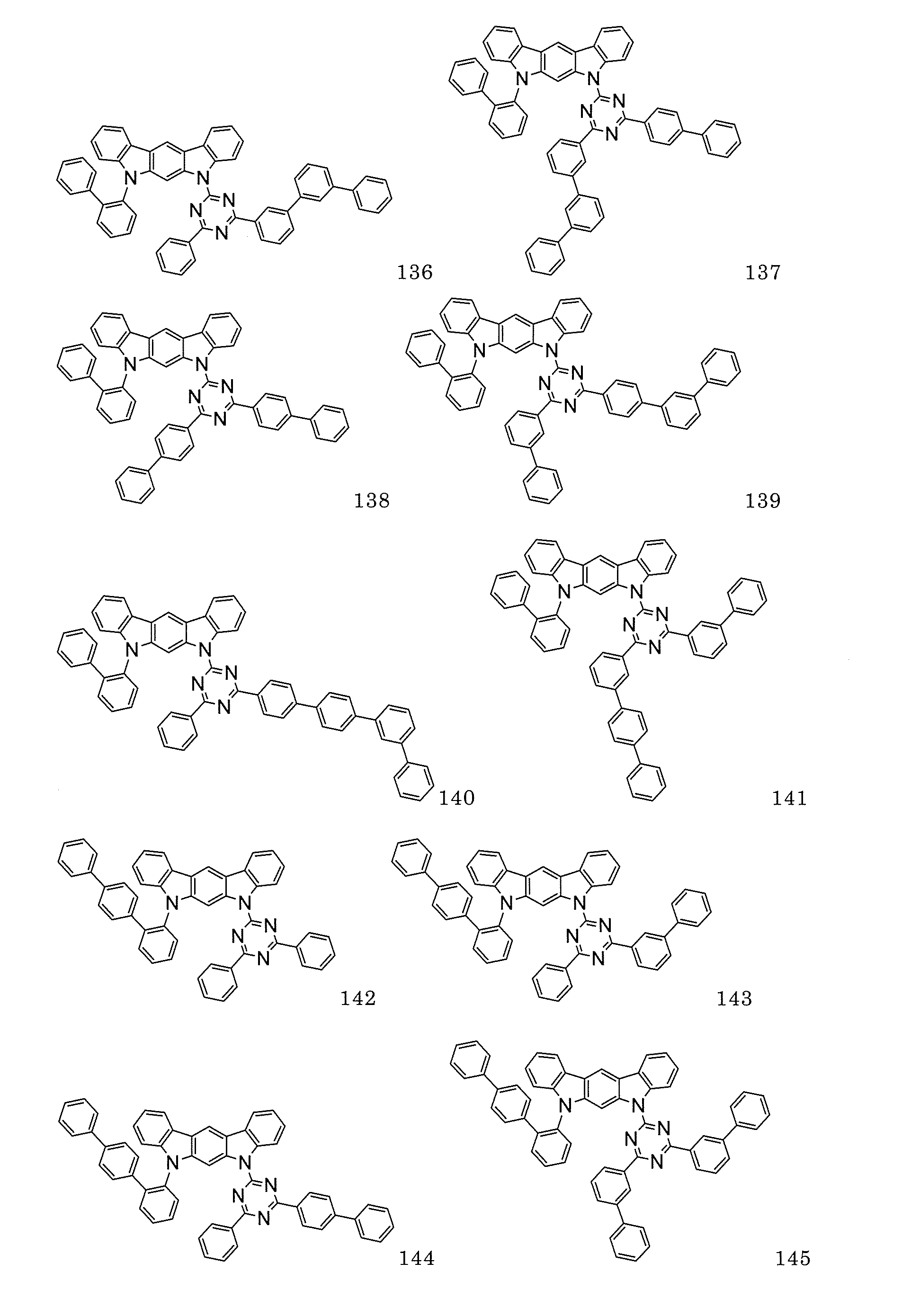
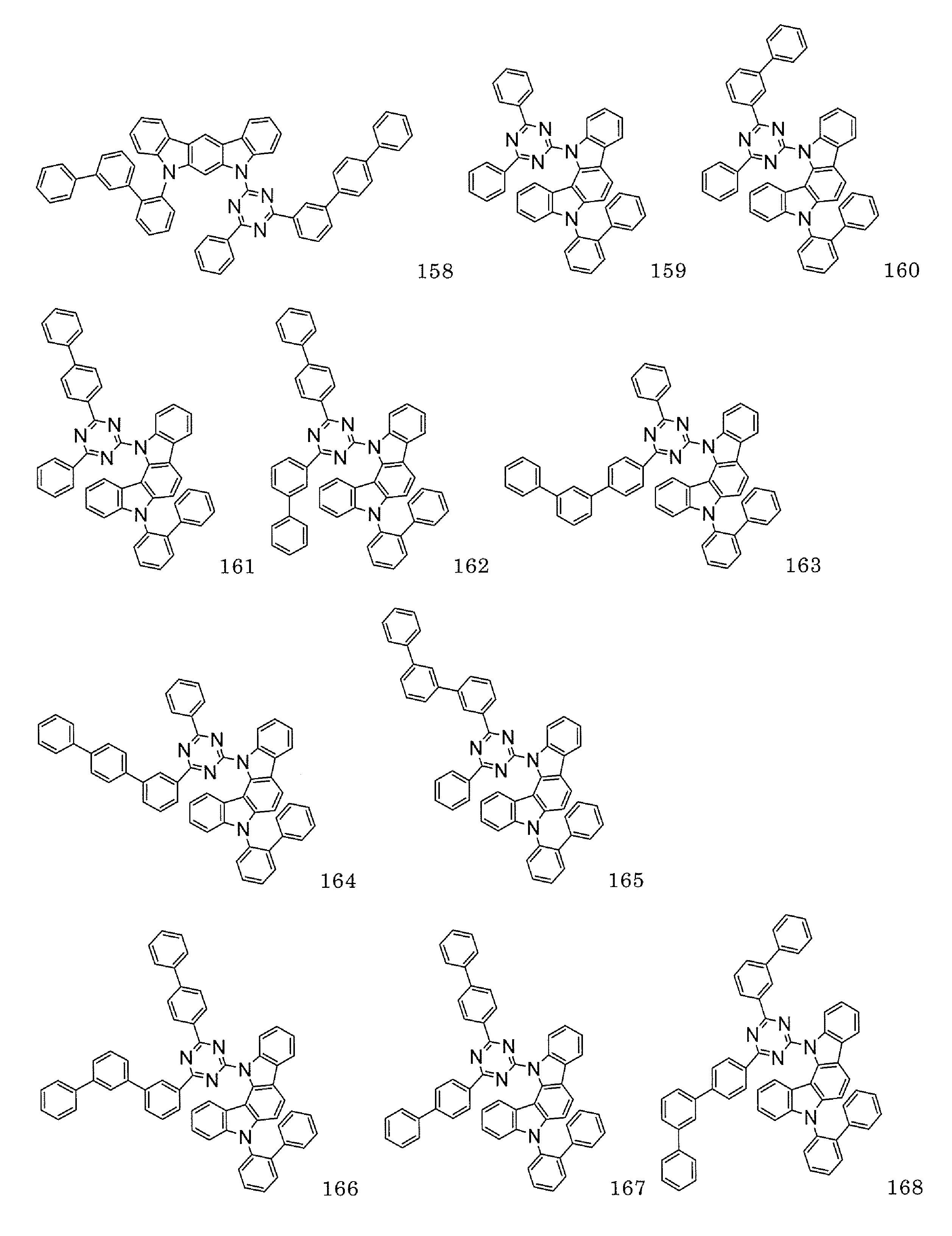
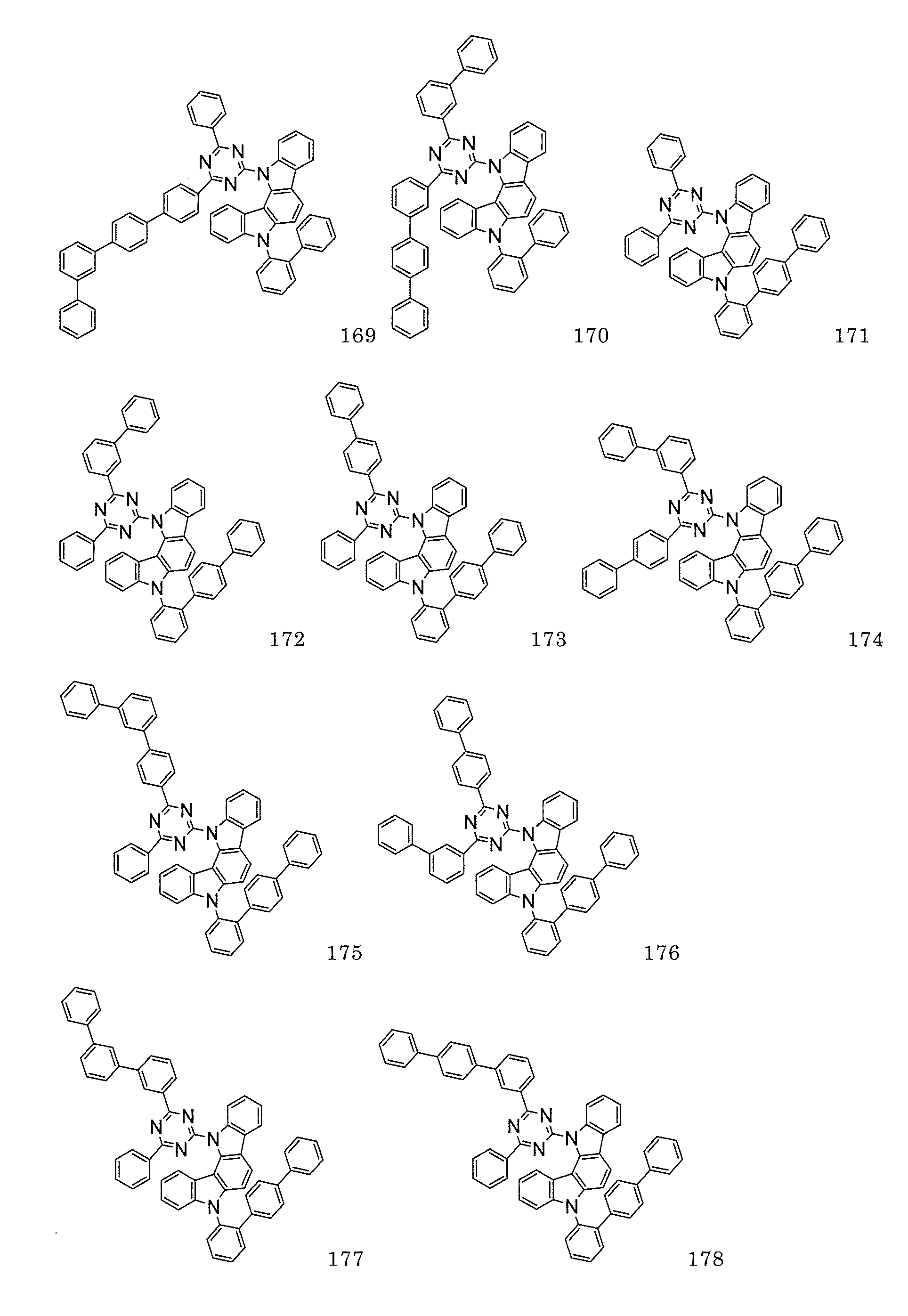
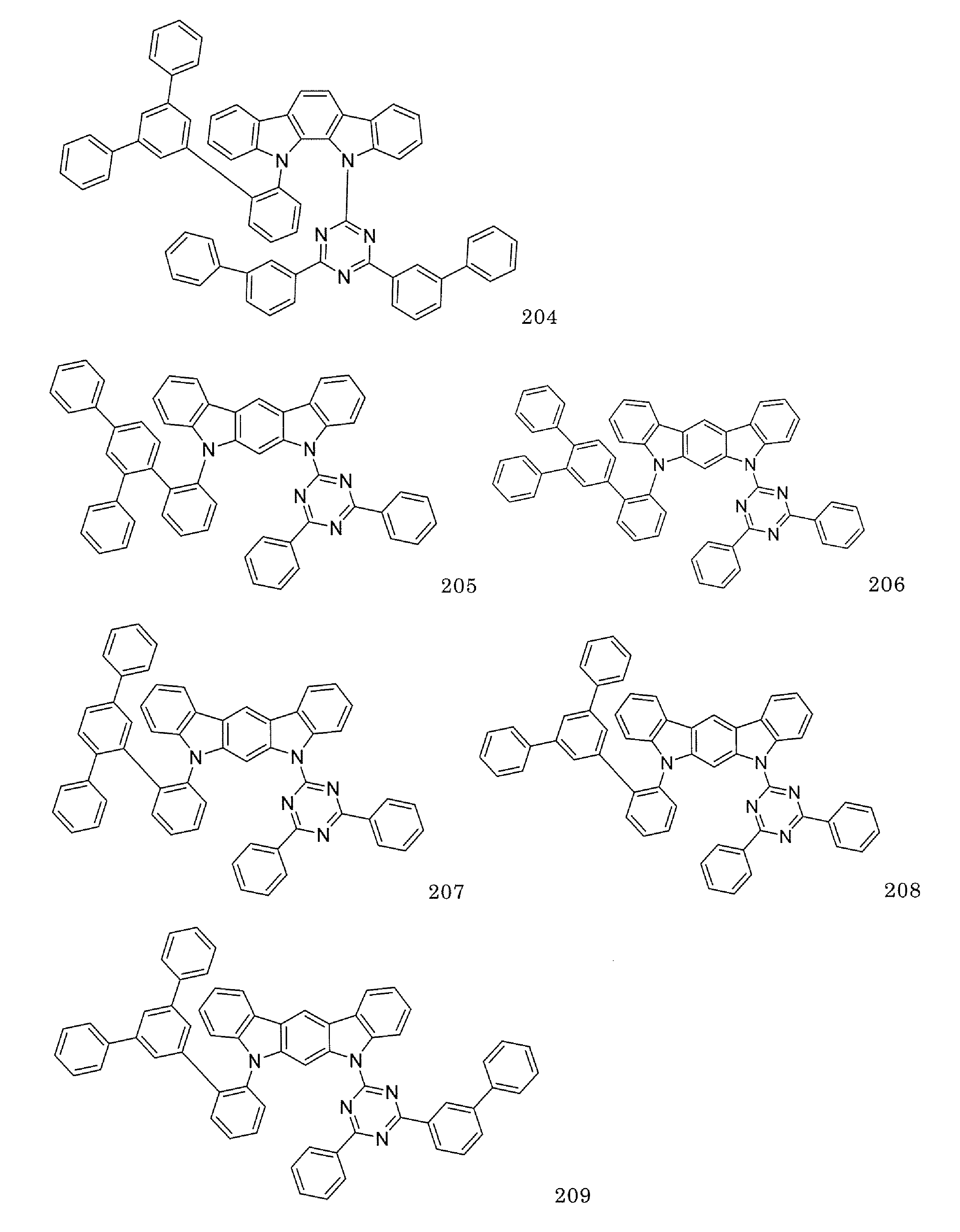
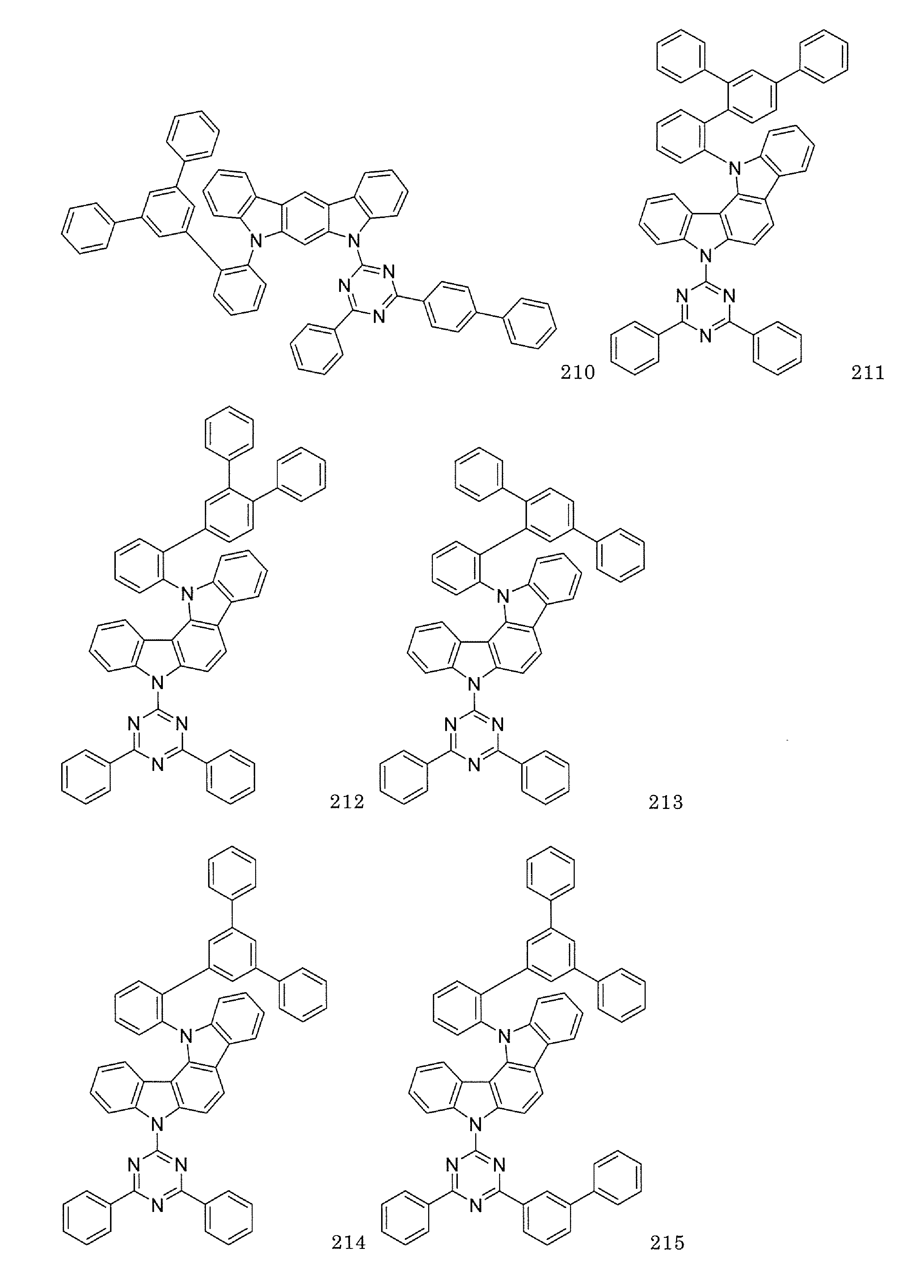
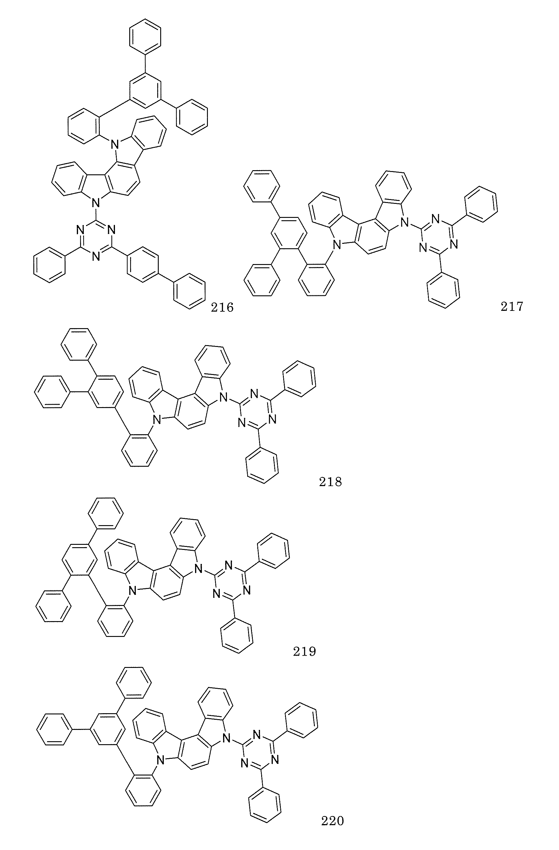
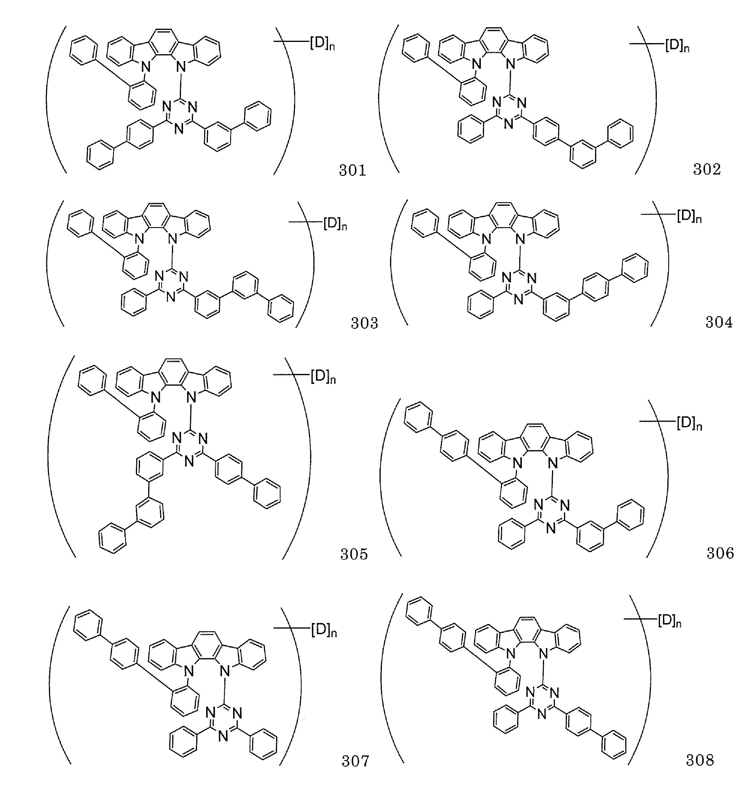
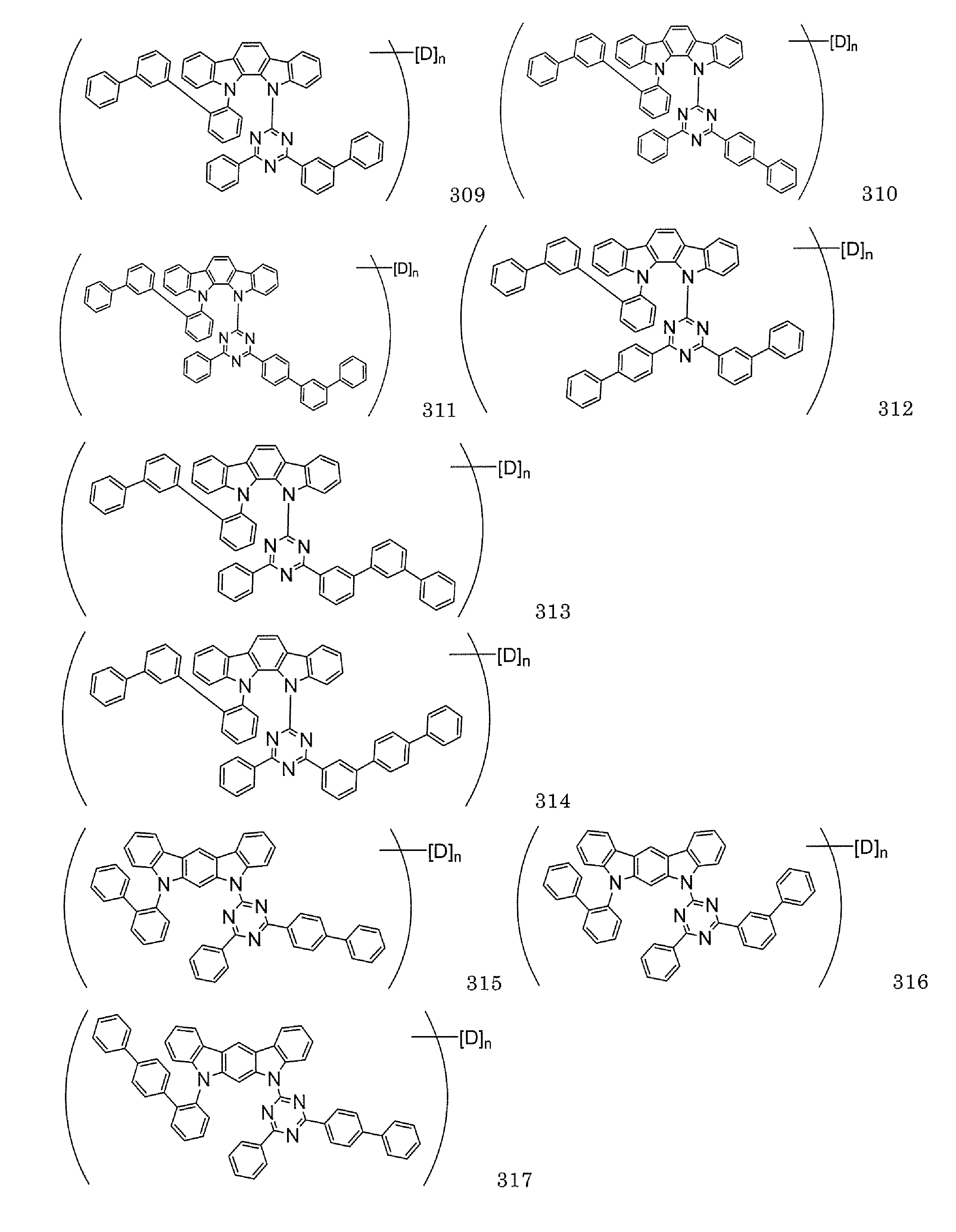
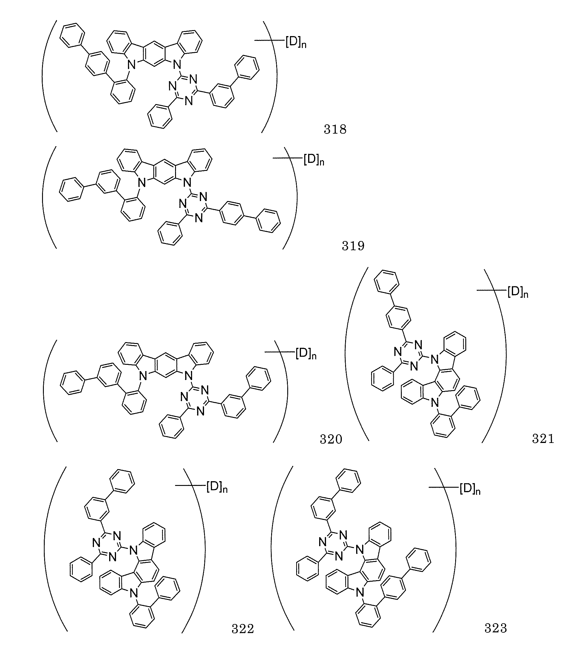
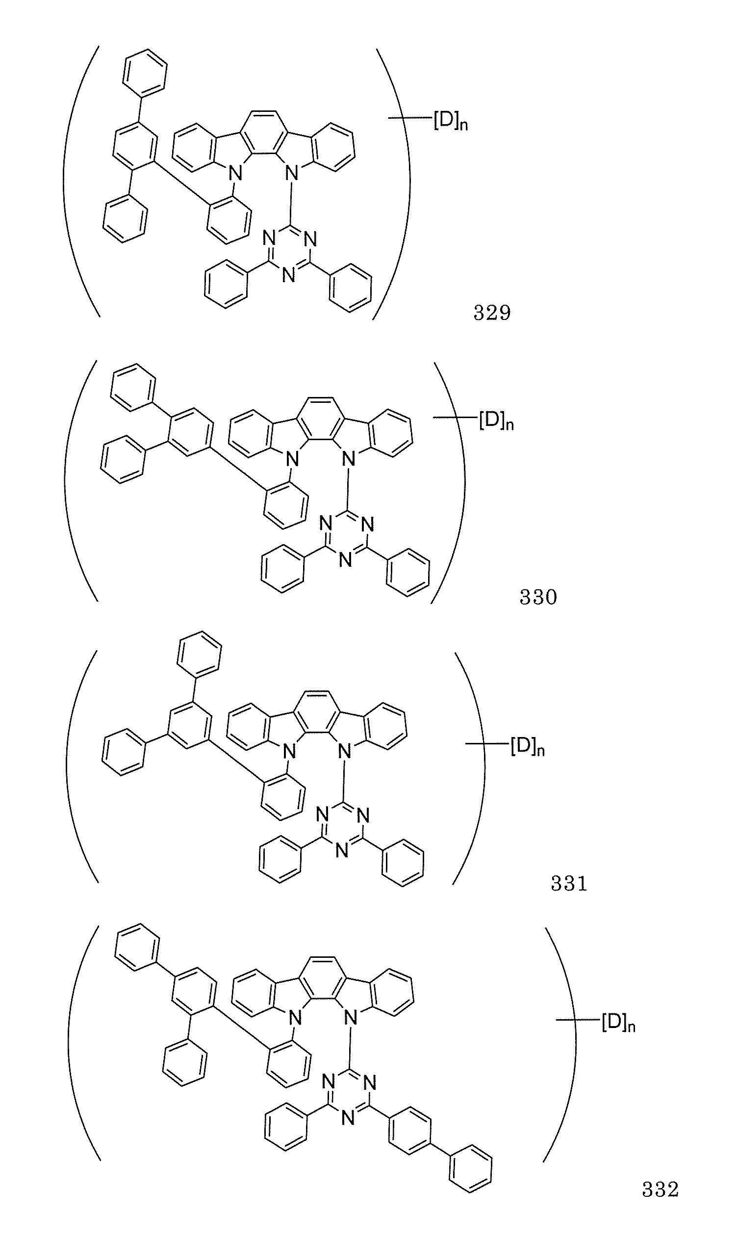
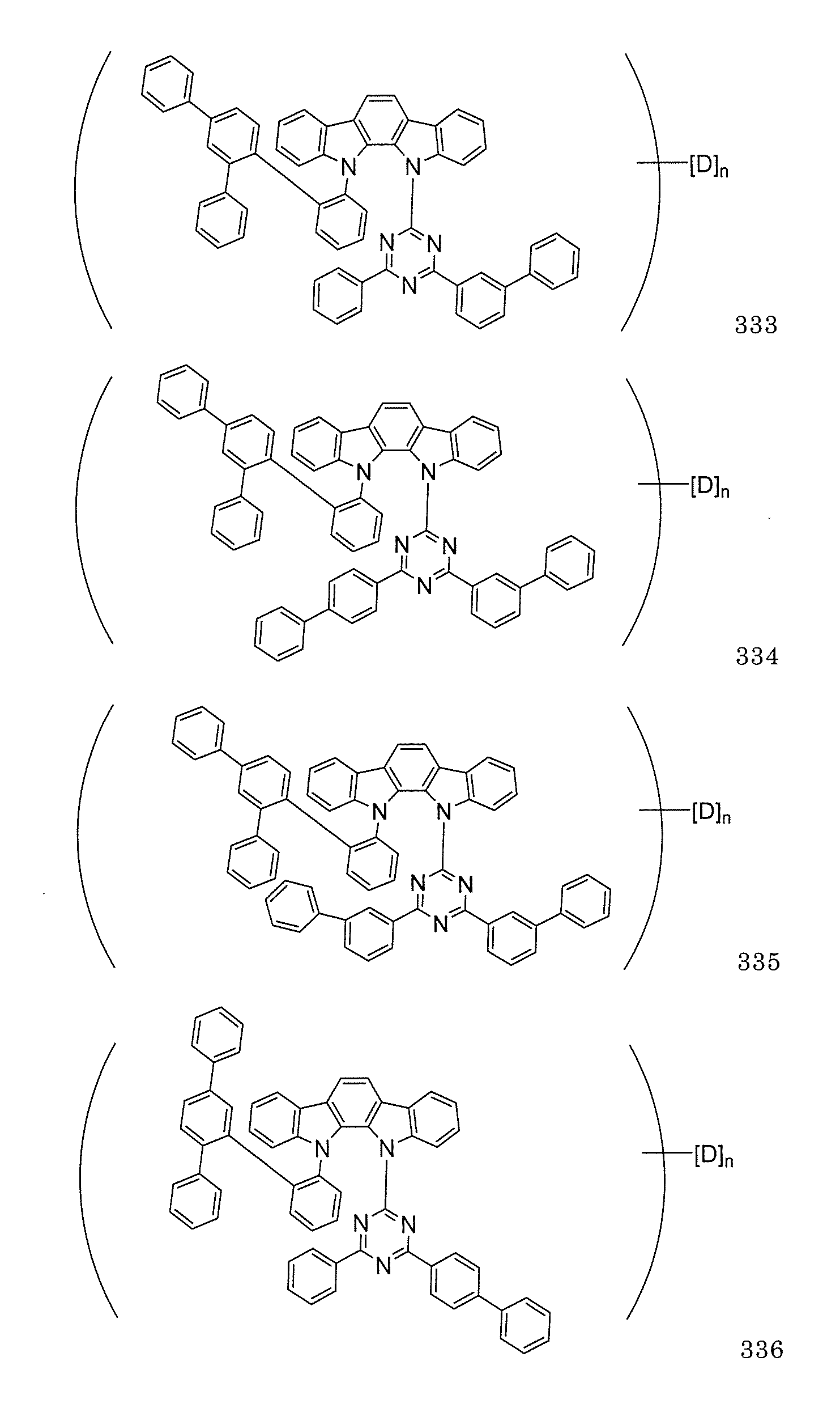
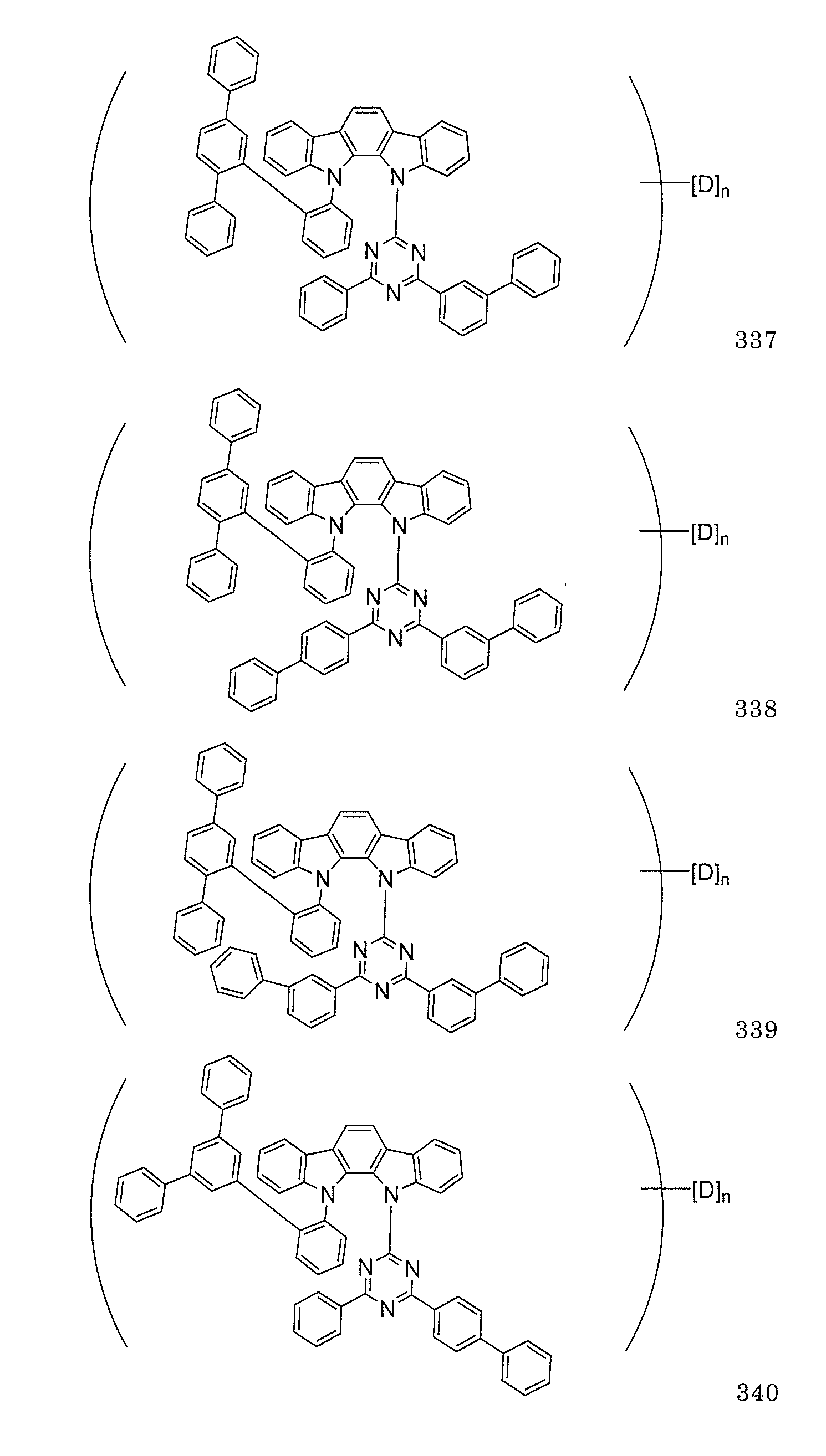
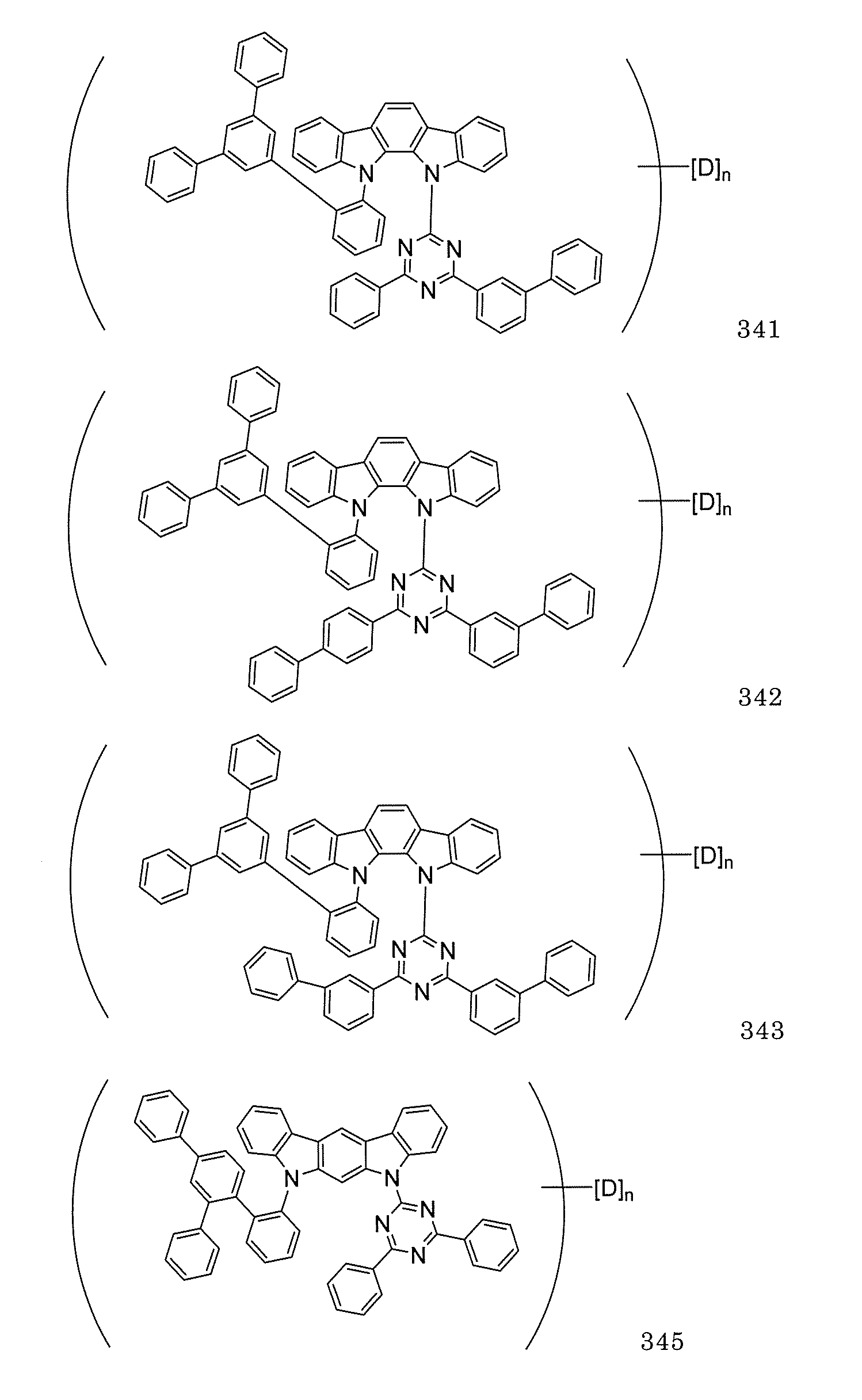
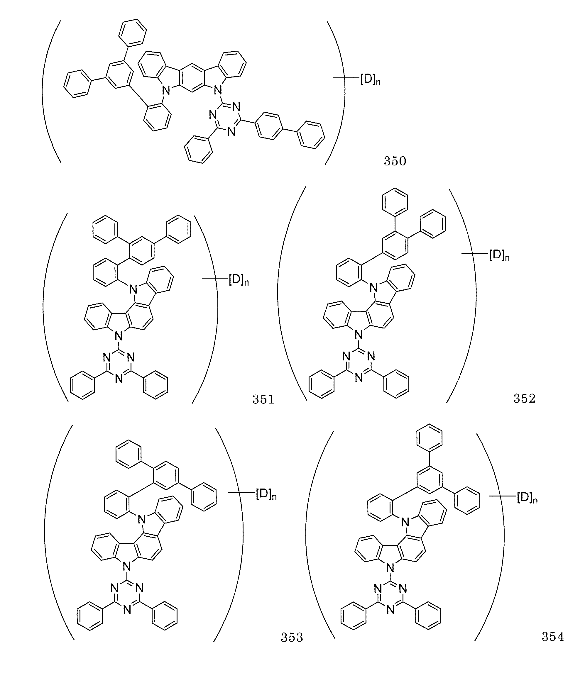
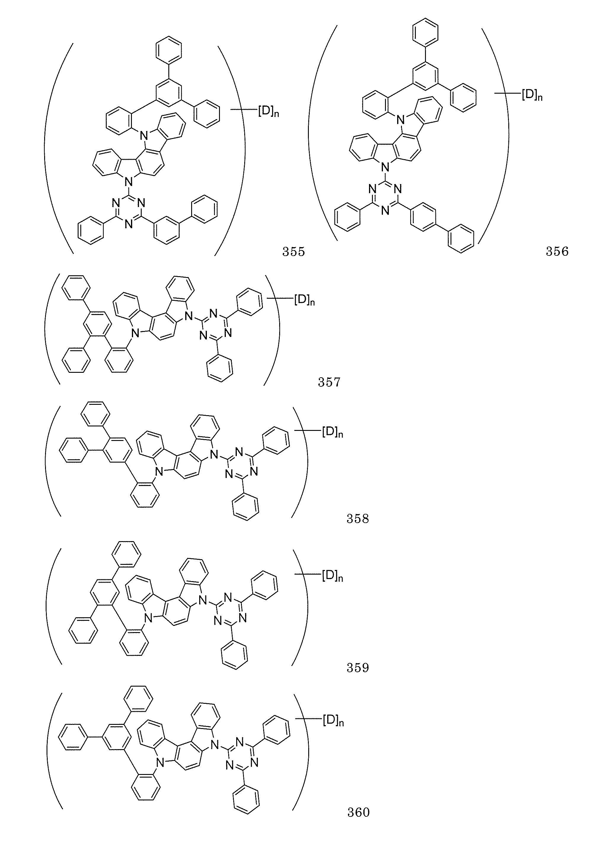
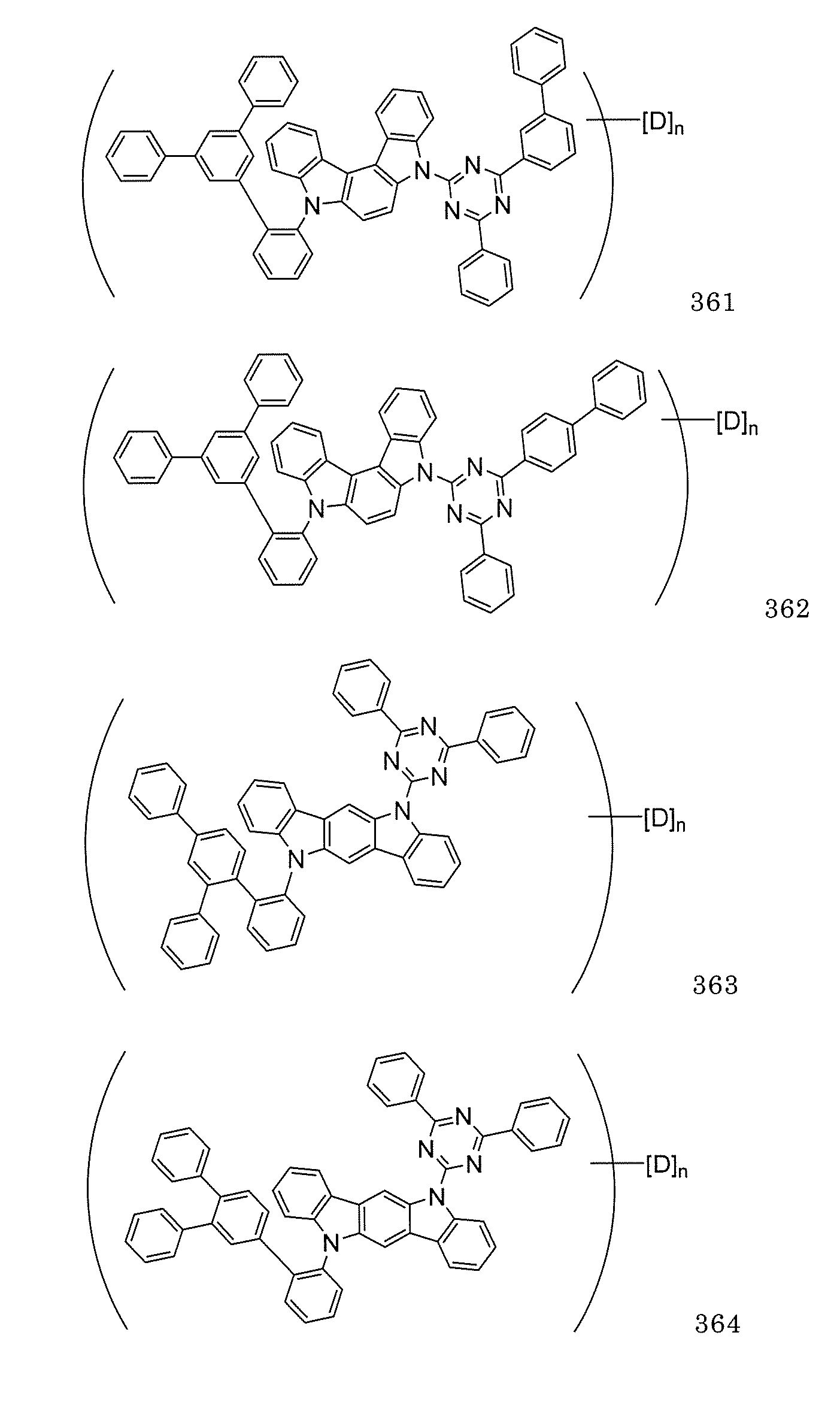
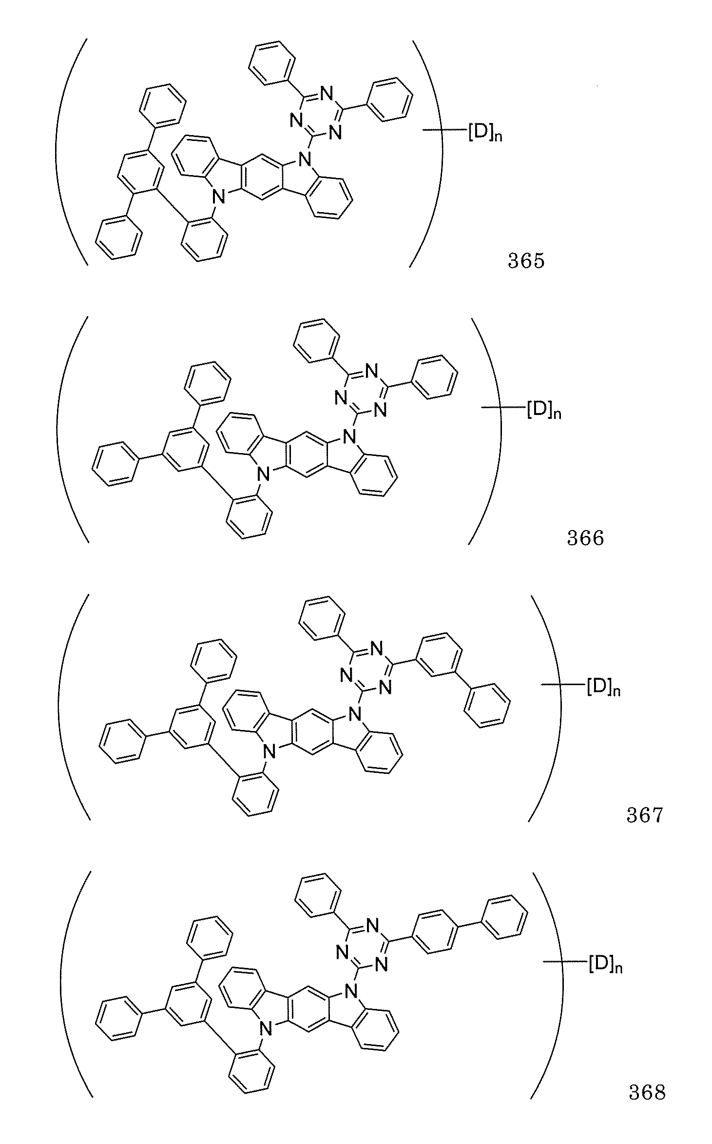
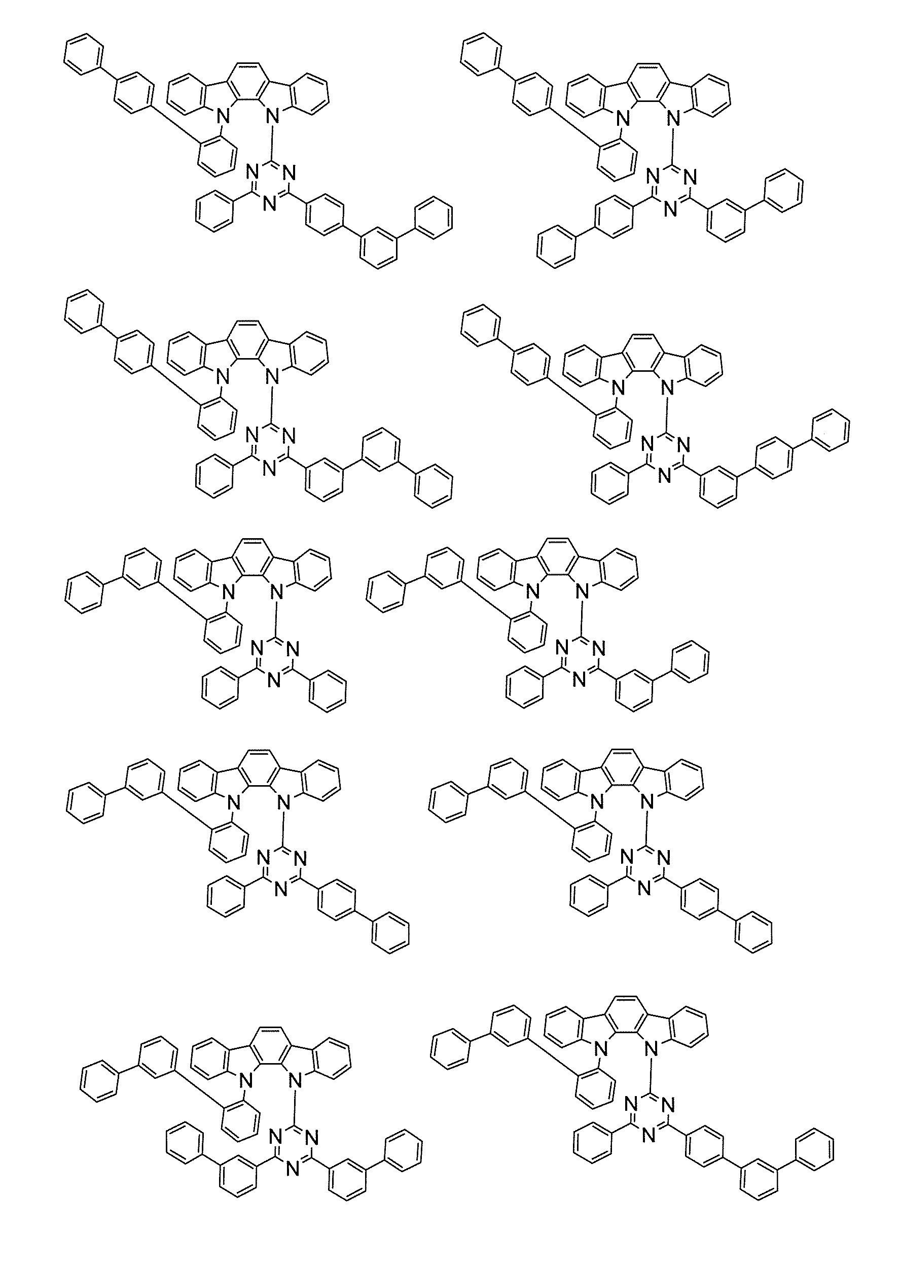
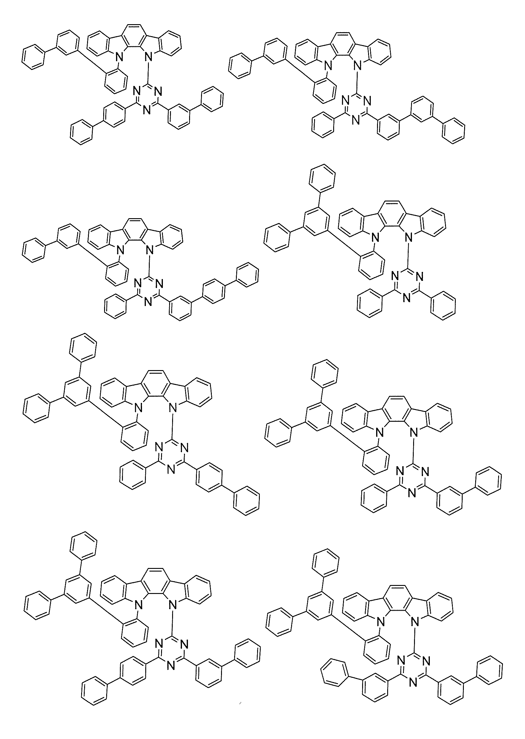
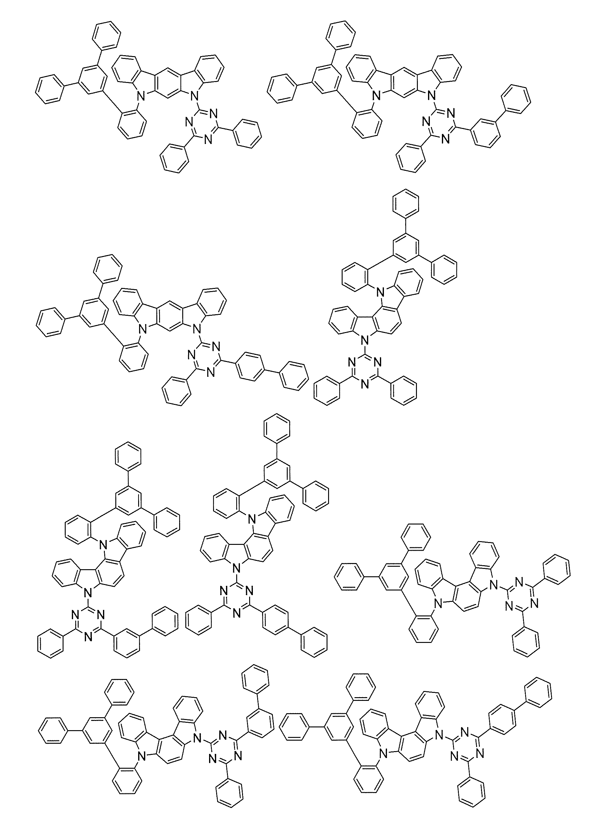
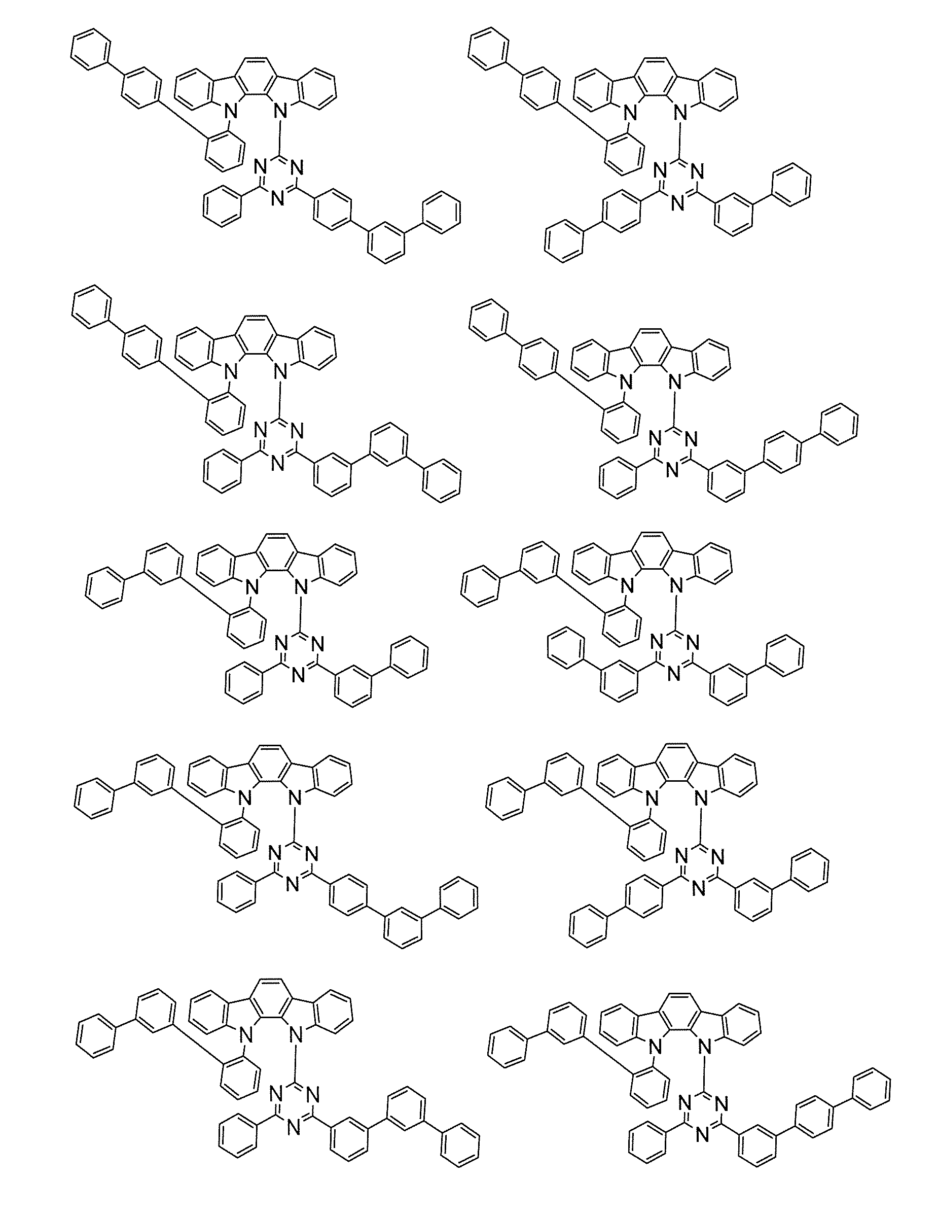
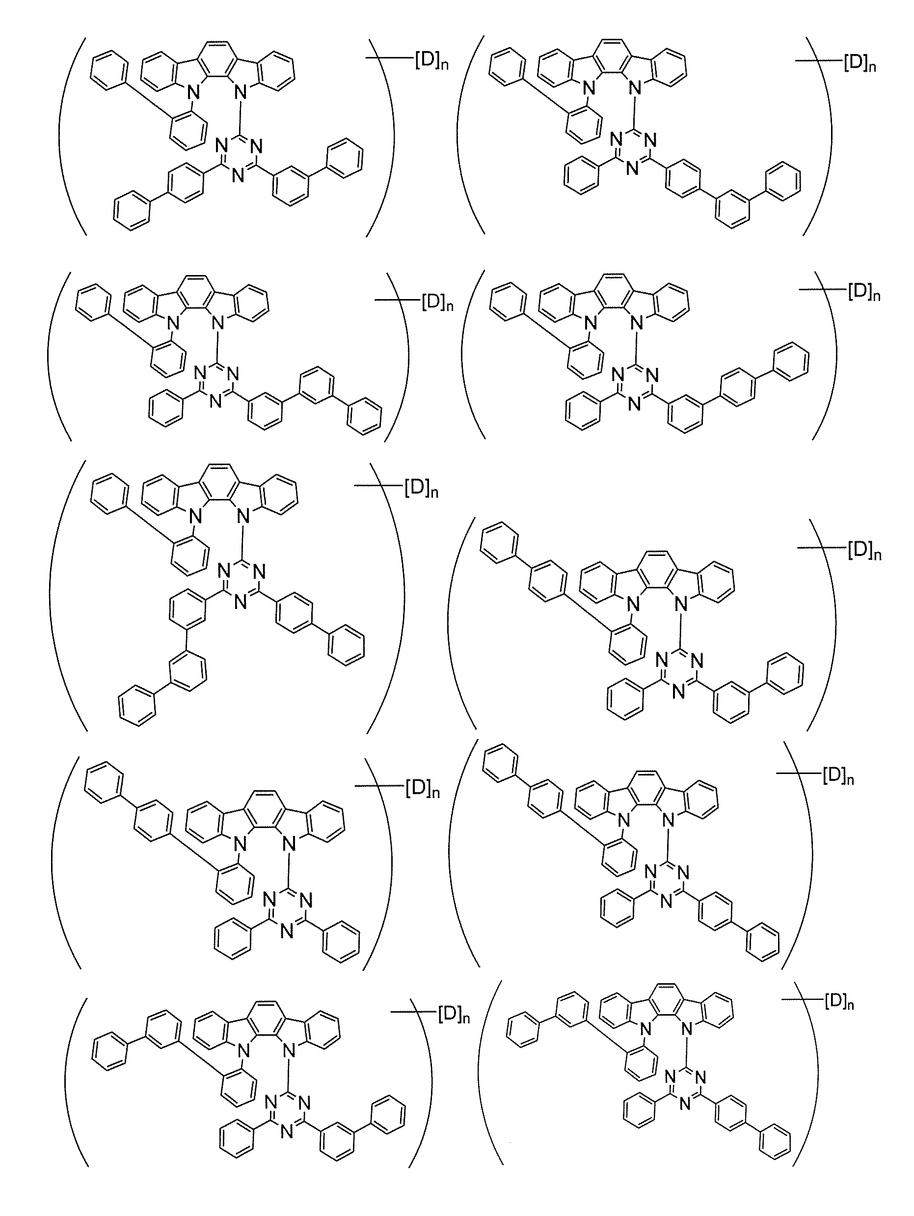
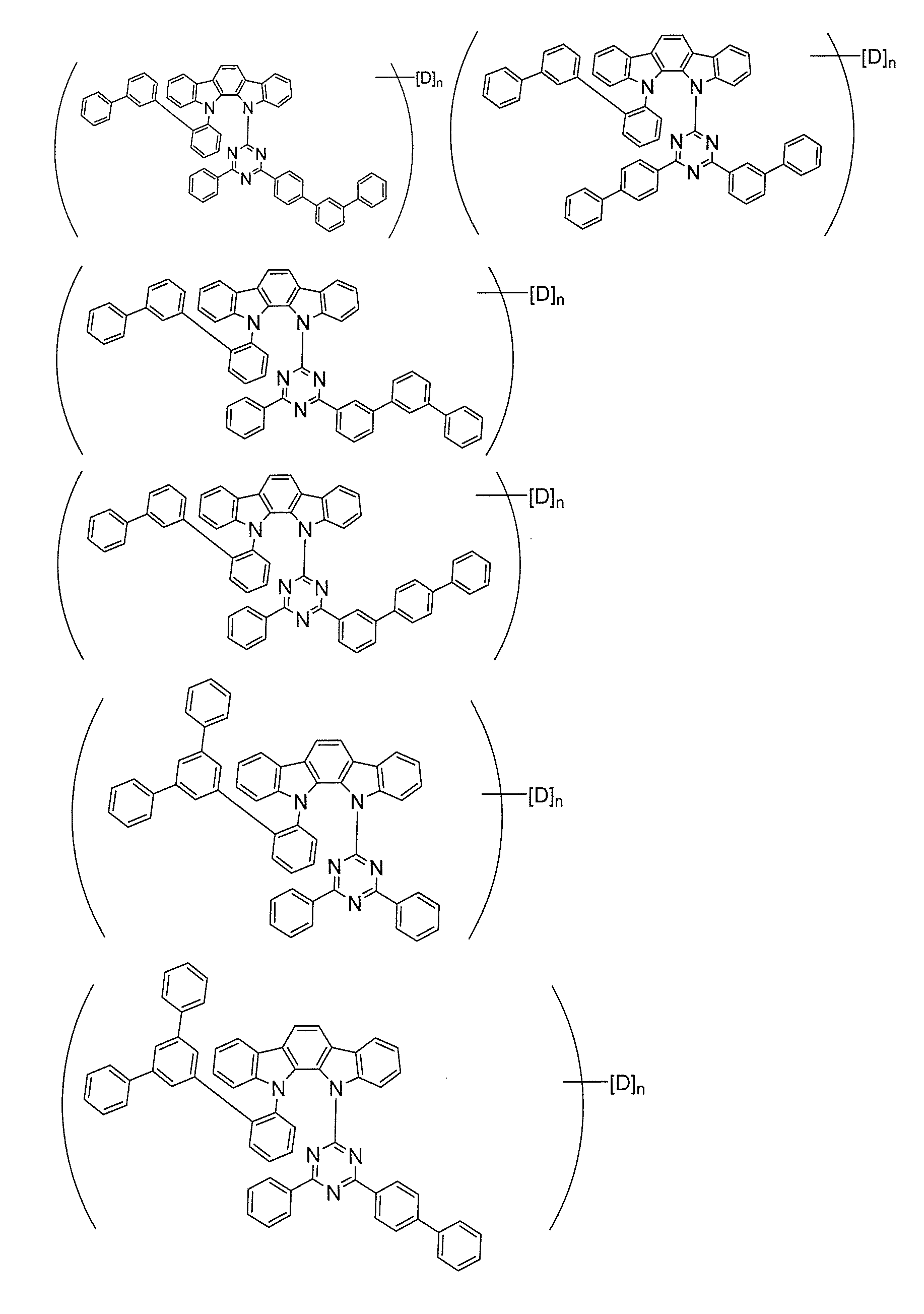
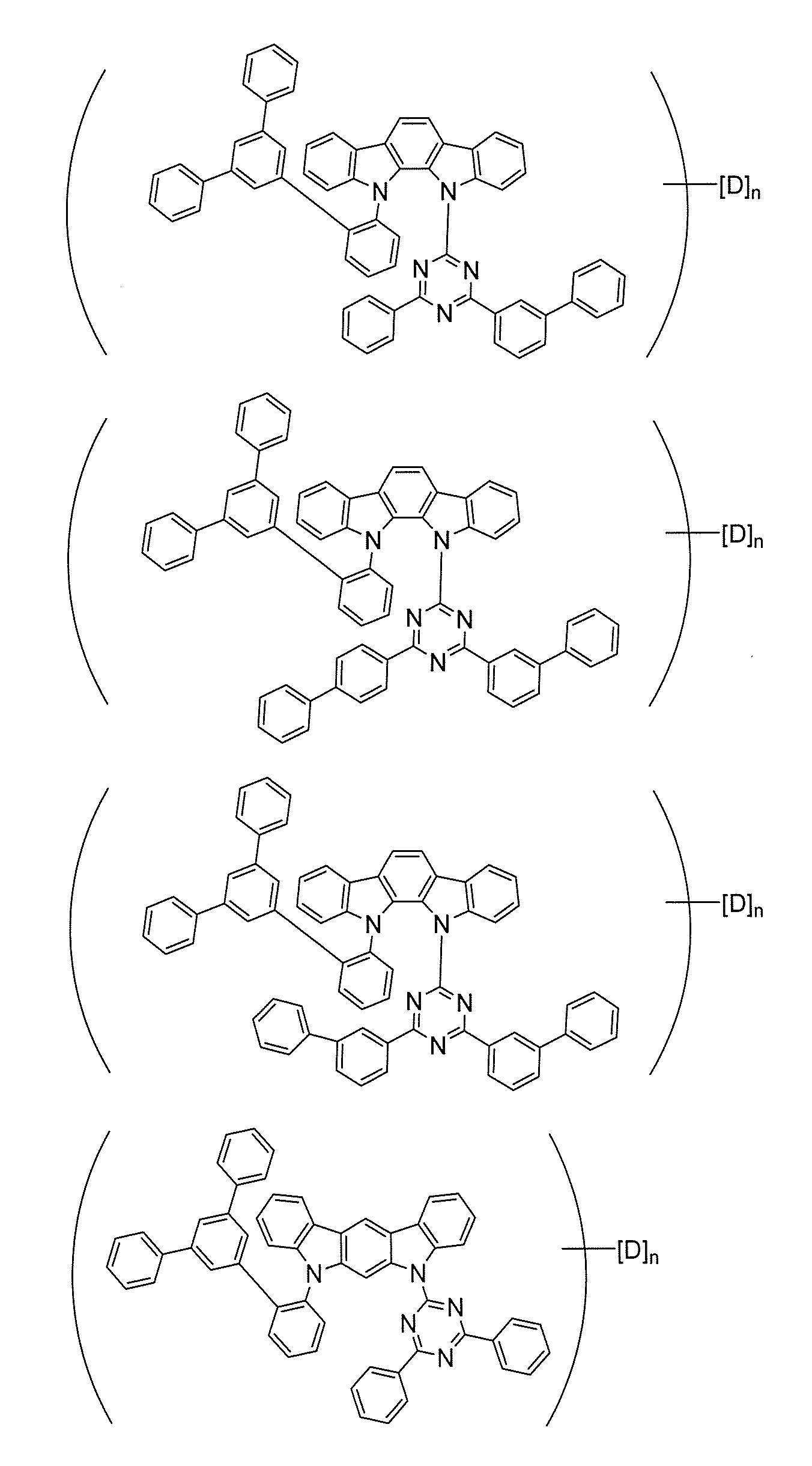
- 前記一般式(1)で表される化合物は、下記からなる群から選択されるいずれか一つである、請求項1に記載の混合組成物。但し、nは置換された重水素(D)の平均の数を表し、平均重水素化率に応じて変化する。


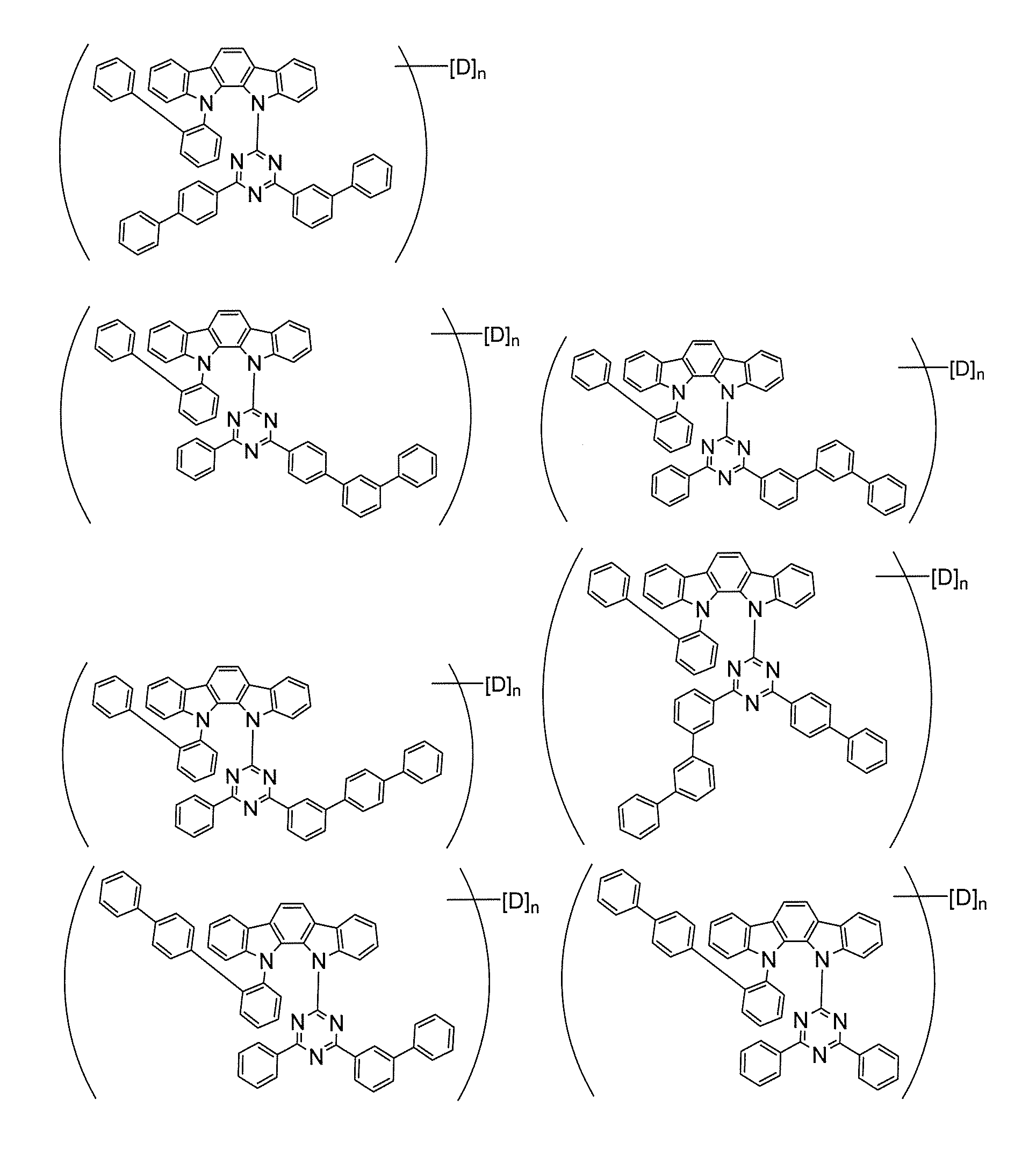
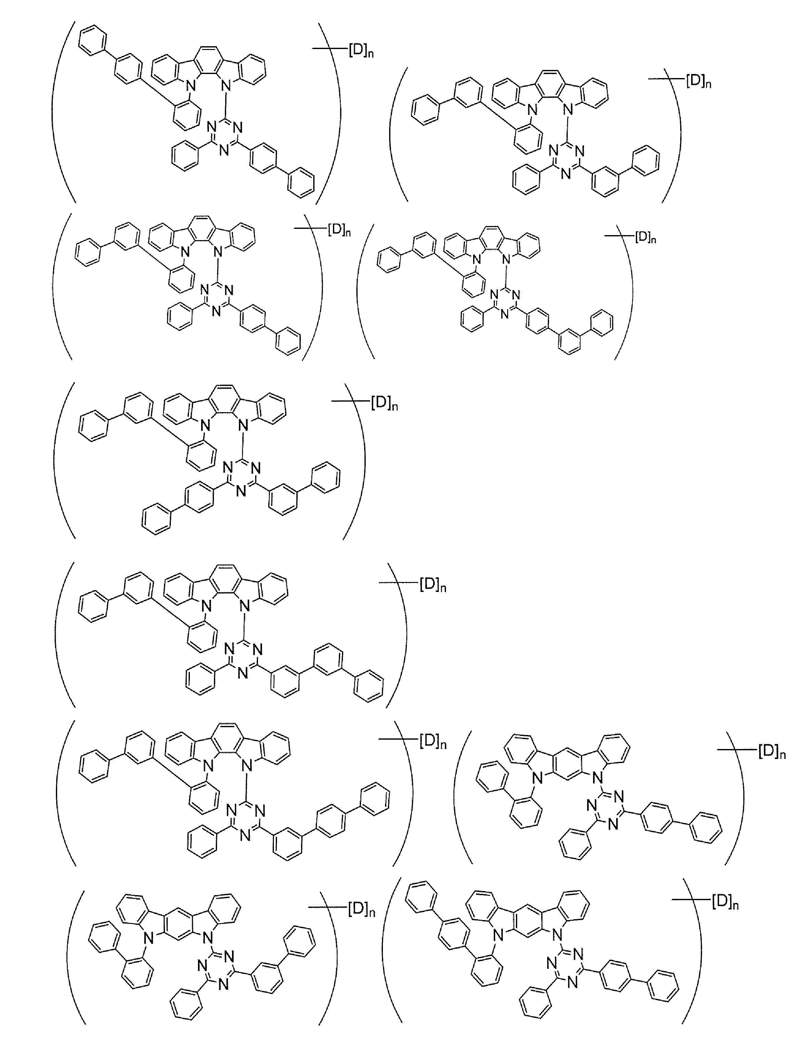
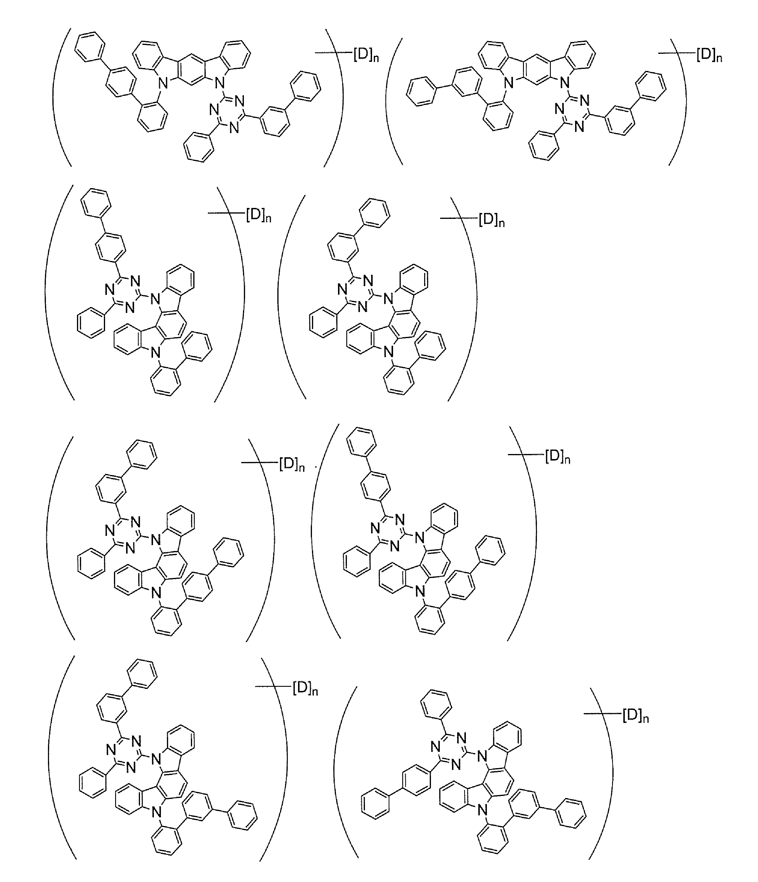


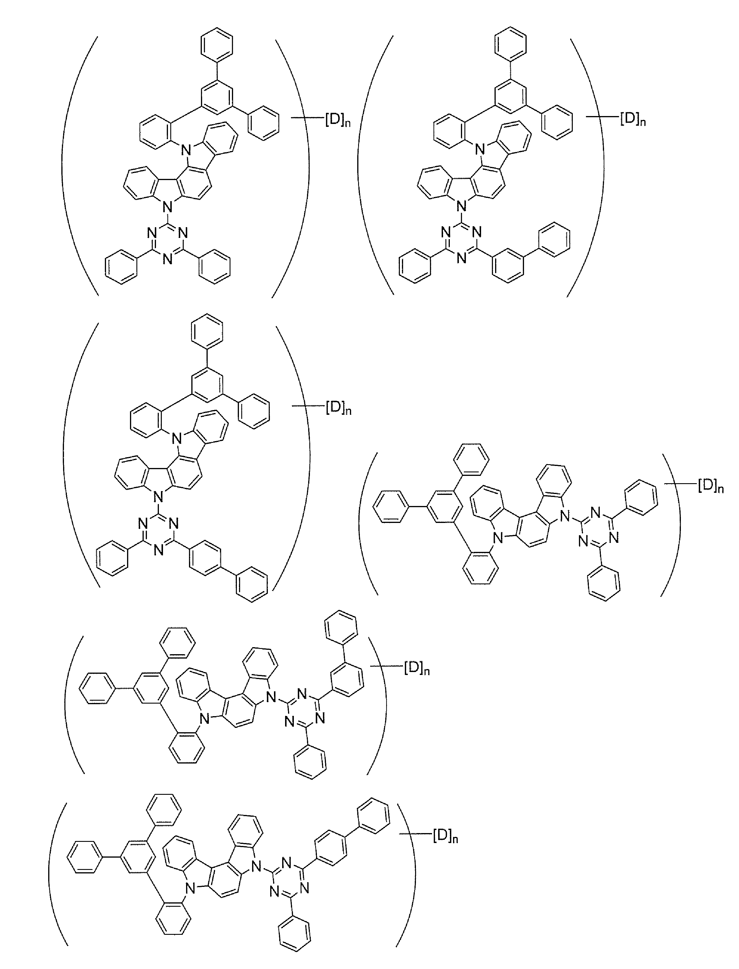
- 前記一般式(1)で表される化合物は、下記からなる群から選択されるいずれか一つである、請求項1記載の混合組成物。但し、nは置換された重水素(D)の平均の数を表し、平均重水素化率に応じて変化する。





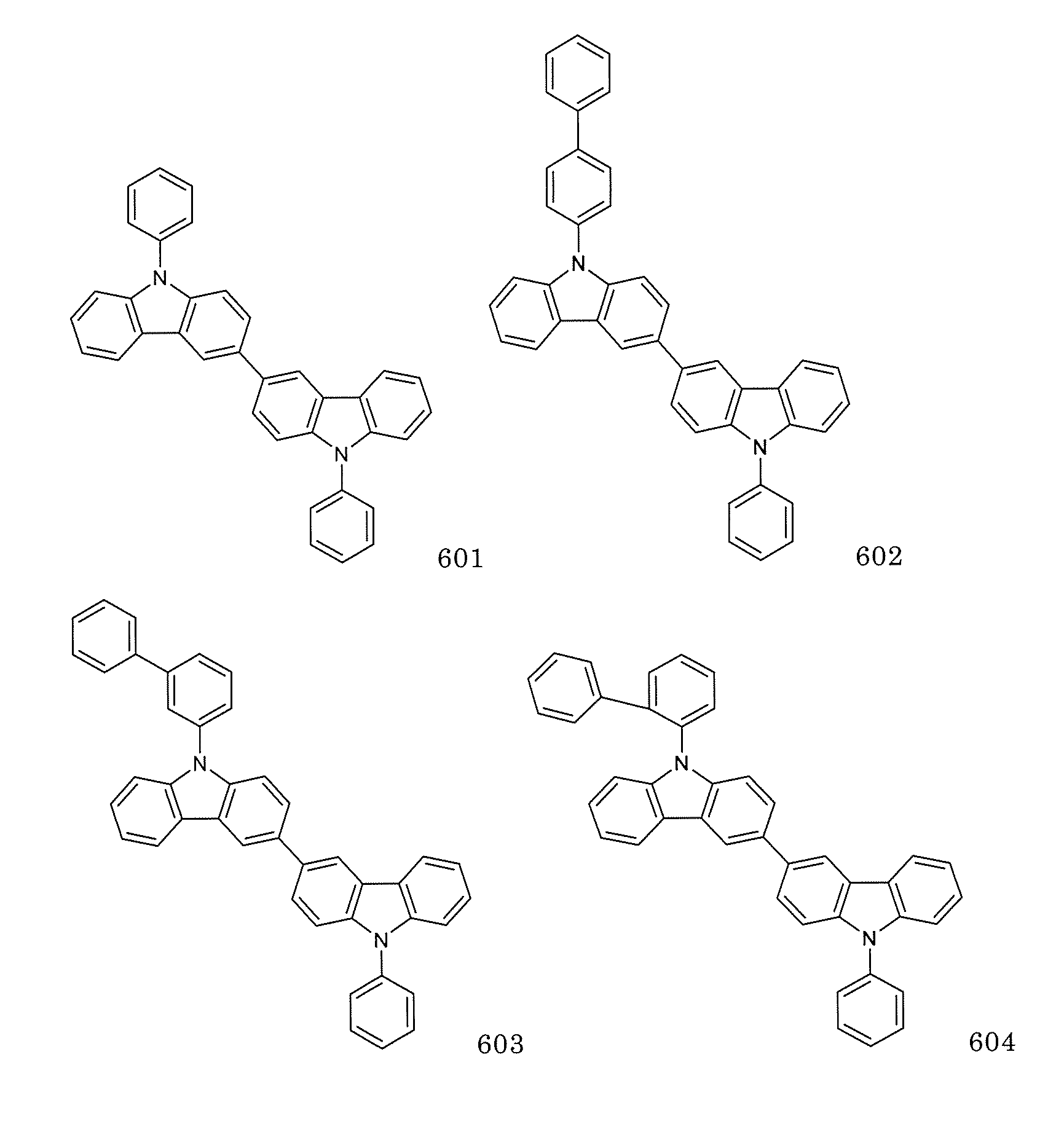
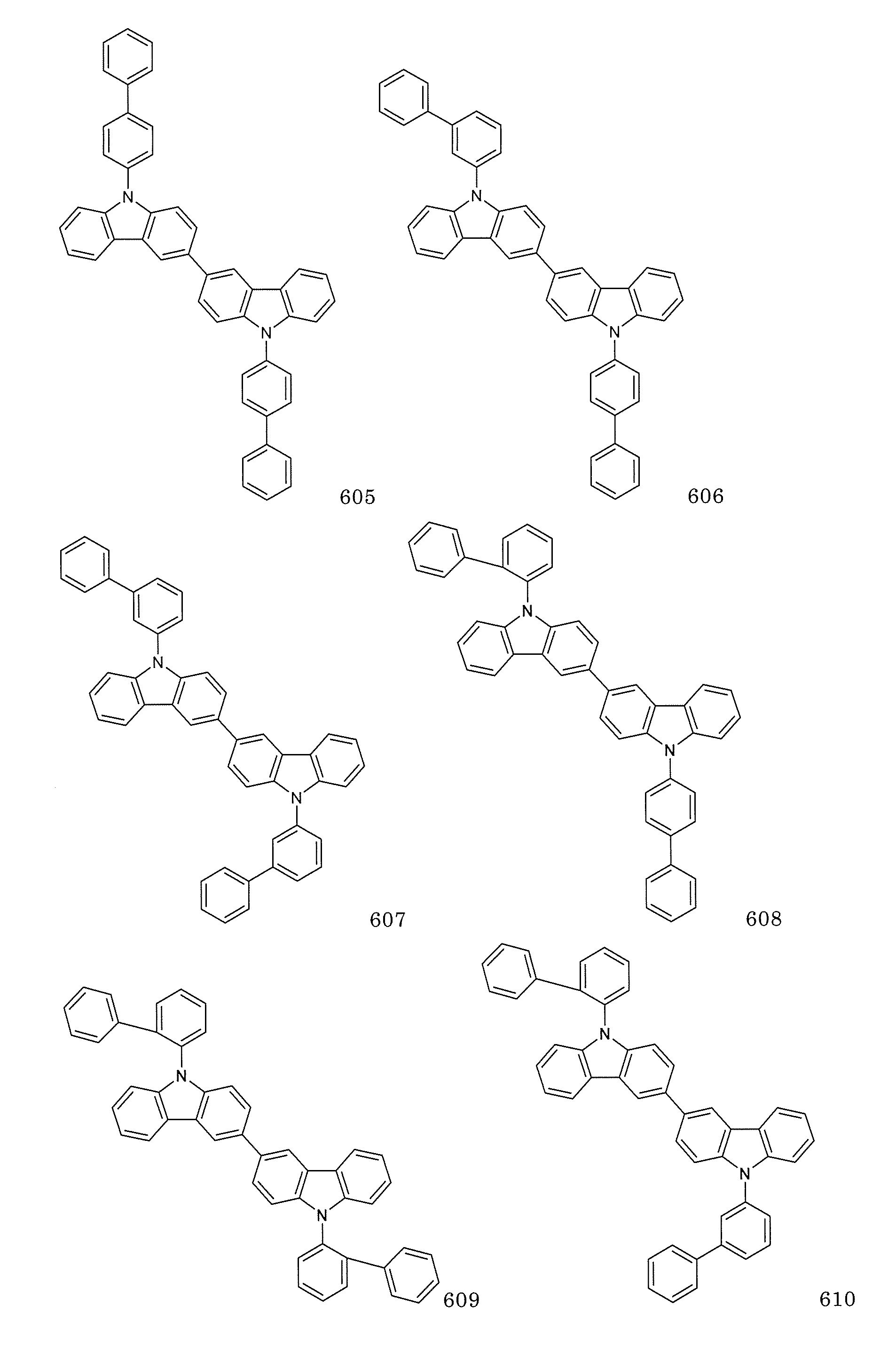
- 前記一般式(2)で表される化合物は、下記からなる群から選択されるいずれか一つである、請求項1記載の混合組成物。但し、mは置換された重水素(D)の平均の数を表し、平均重水素化率に応じて変化する。

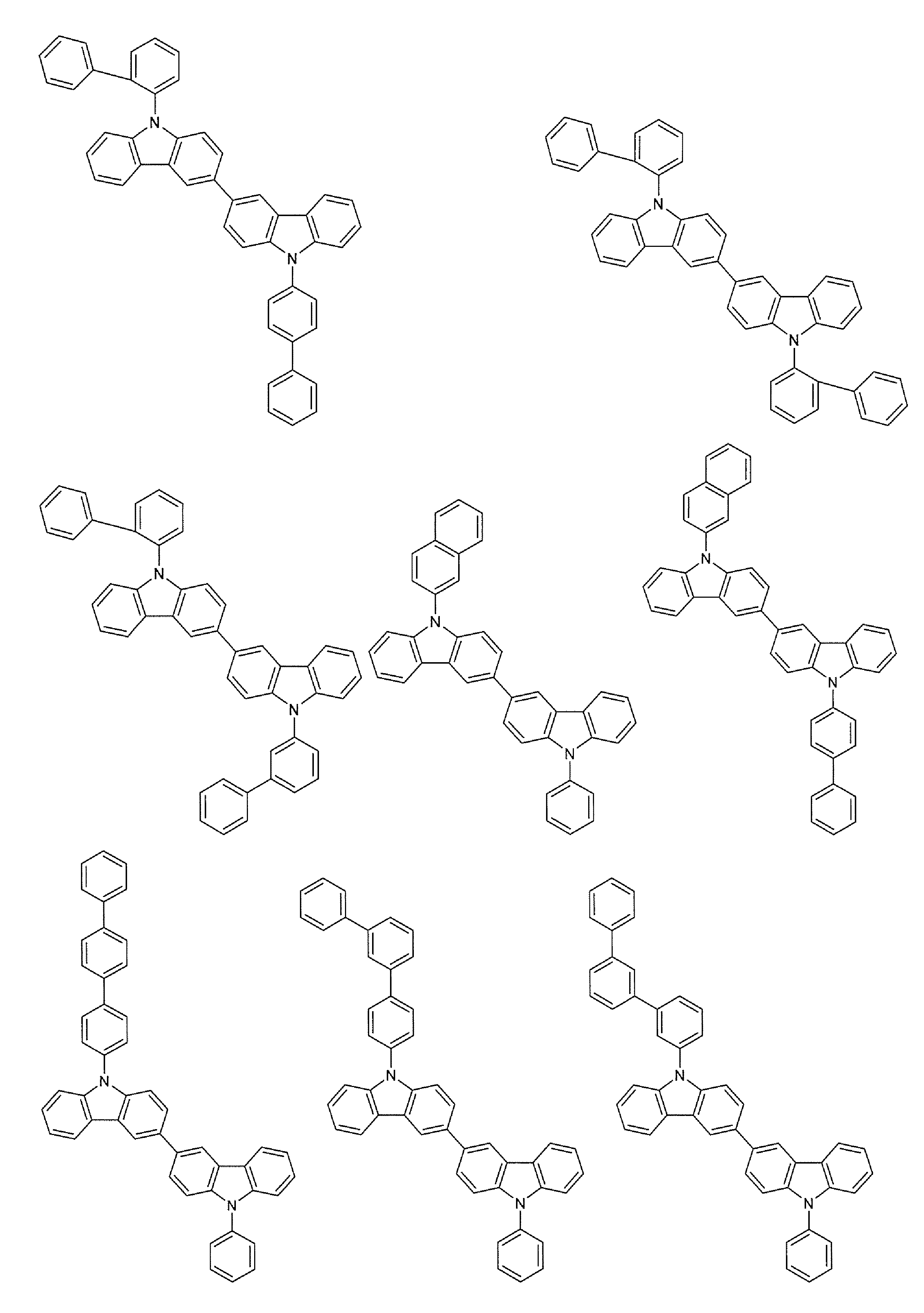
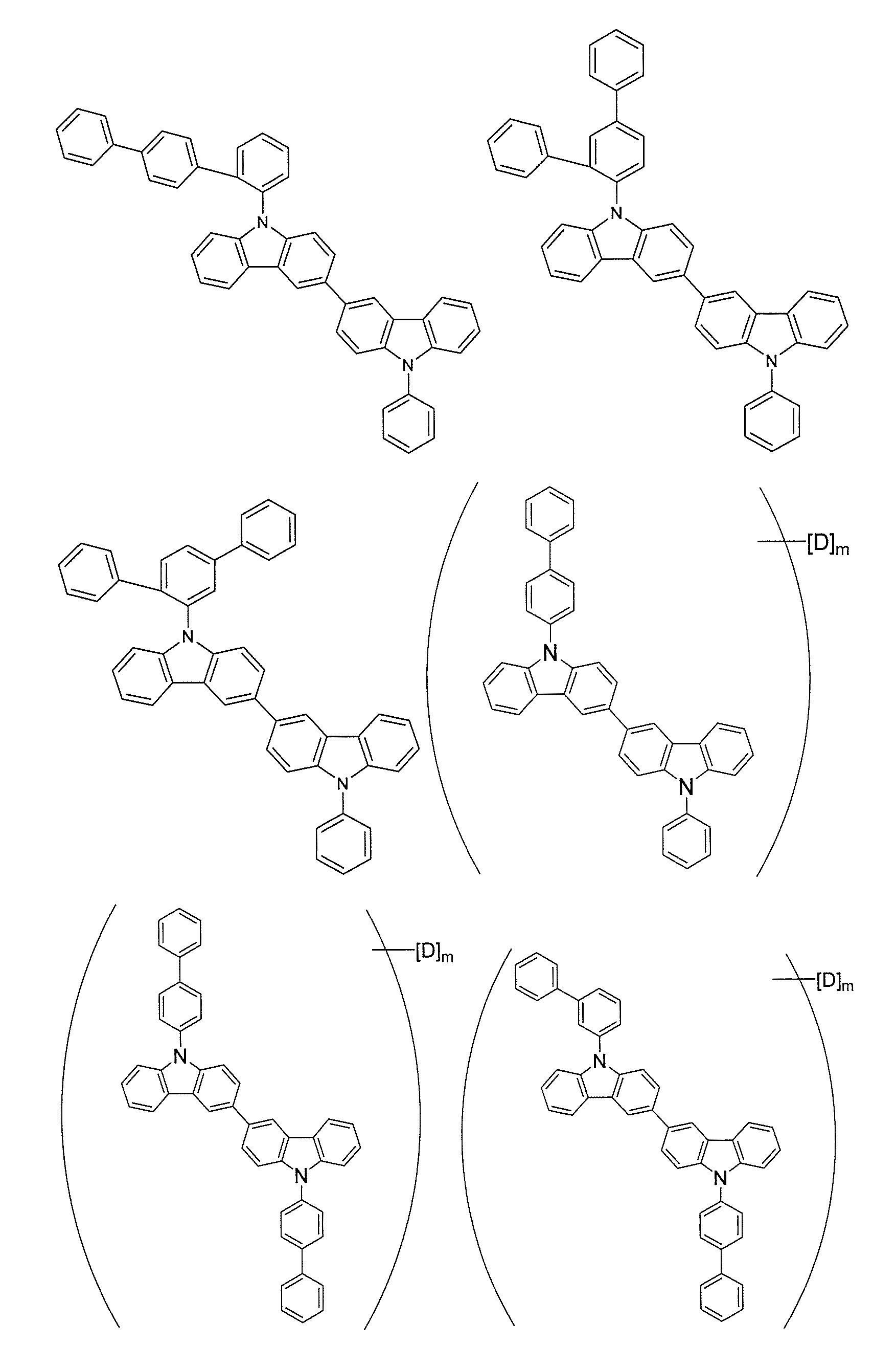

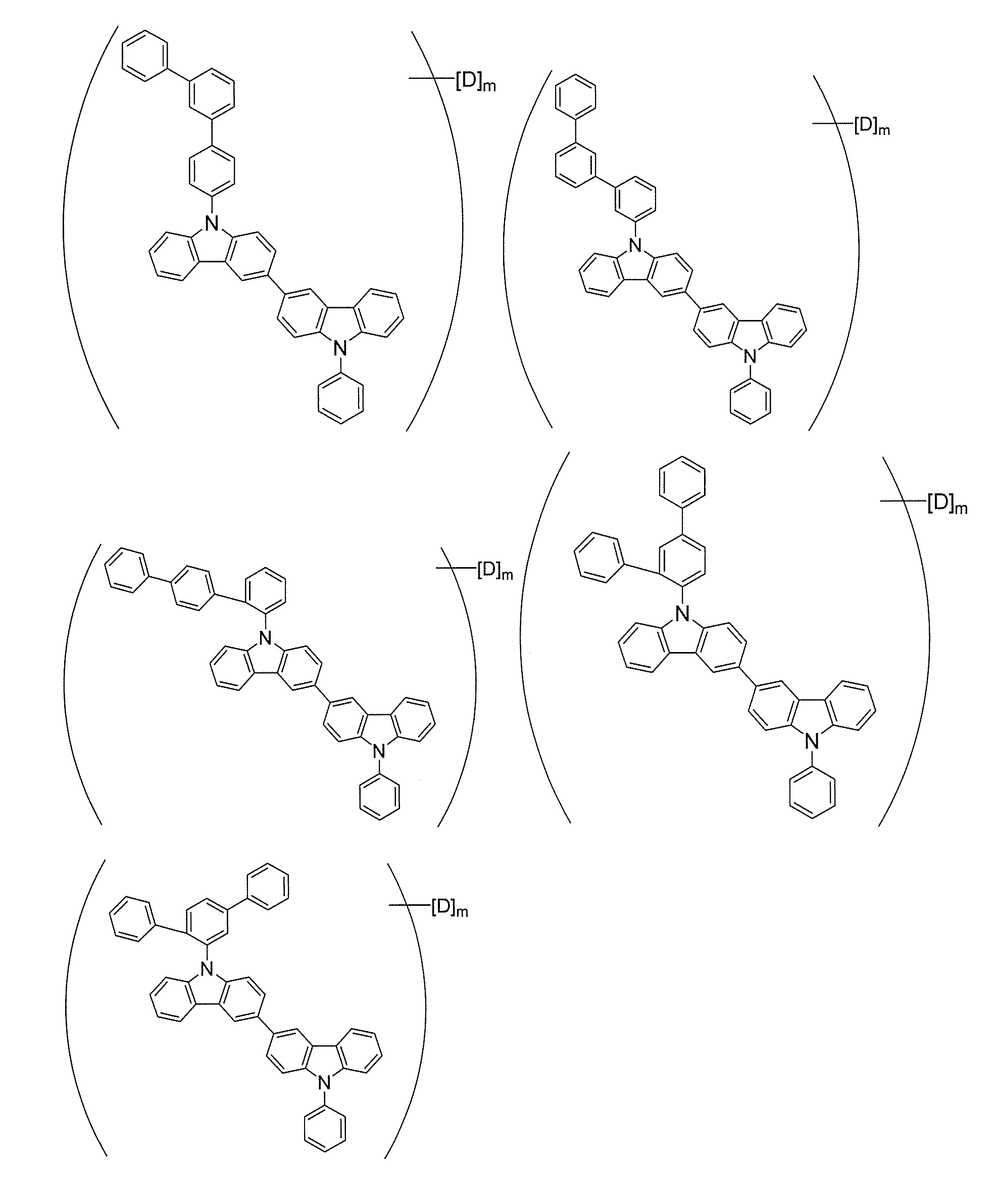
Priority Applications (3)
| Application Number | Priority Date | Filing Date | Title |
|---|---|---|---|
| CN202380084077.9A CN120323116A (zh) | 2023-01-11 | 2023-12-26 | 混合组合物及有机电场发光元件 |
| KR1020257026289A KR20250133930A (ko) | 2023-01-11 | 2023-12-26 | 혼합 조성물 및 유기 전계 발광 소자 |
| JP2024570146A JPWO2024150673A1 (ja) | 2023-01-11 | 2023-12-26 |
Applications Claiming Priority (2)
| Application Number | Priority Date | Filing Date | Title |
|---|---|---|---|
| JP2023002255 | 2023-01-11 | ||
| JP2023-002255 | 2023-01-11 |
Publications (1)
| Publication Number | Publication Date |
|---|---|
| WO2024150673A1 true WO2024150673A1 (ja) | 2024-07-18 |
Family
ID=91896973
Family Applications (1)
| Application Number | Title | Priority Date | Filing Date |
|---|---|---|---|
| PCT/JP2023/046770 Ceased WO2024150673A1 (ja) | 2023-01-11 | 2023-12-26 | 混合組成物及び有機電界発光素子 |
Country Status (4)
| Country | Link |
|---|---|
| JP (1) | JPWO2024150673A1 (ja) |
| KR (1) | KR20250133930A (ja) |
| CN (1) | CN120323116A (ja) |
| WO (1) | WO2024150673A1 (ja) |
Cited By (1)
| Publication number | Priority date | Publication date | Assignee | Title |
|---|---|---|---|---|
| WO2025164666A1 (ja) * | 2024-01-31 | 2025-08-07 | 日鉄ケミカル&マテリアル株式会社 | 有機電界発光素子 |
Citations (4)
| Publication number | Priority date | Publication date | Assignee | Title |
|---|---|---|---|---|
| KR20210112885A (ko) * | 2020-03-06 | 2021-09-15 | 삼성에스디아이 주식회사 | 유기 광전자 소자용 조성물, 유기 광전자 소자 및 표시 장치 |
| KR20220015980A (ko) * | 2020-07-31 | 2022-02-08 | 주식회사 엘지화학 | 유기 발광 소자 |
| WO2022131123A1 (ja) * | 2020-12-18 | 2022-06-23 | 日鉄ケミカル&マテリアル株式会社 | 有機電界発光素子及びその製造方法 |
| WO2022149493A1 (ja) * | 2021-01-08 | 2022-07-14 | 日鉄ケミカル&マテリアル株式会社 | 有機電界発光素子及びその製造方法 |
Family Cites Families (13)
| Publication number | Priority date | Publication date | Assignee | Title |
|---|---|---|---|---|
| JP2003133075A (ja) | 2001-07-25 | 2003-05-09 | Toray Ind Inc | 発光素子 |
| US8062769B2 (en) | 2006-11-09 | 2011-11-22 | Nippon Steel Chemical Co., Ltd. | Indolocarbazole compound for use in organic electroluminescent device and organic electroluminescent device |
| JP5484690B2 (ja) | 2007-05-18 | 2014-05-07 | ユー・ディー・シー アイルランド リミテッド | 有機電界発光素子 |
| US20100295444A1 (en) | 2009-05-22 | 2010-11-25 | Idemitsu Kosan Co., Ltd. | Organic electroluminescence device |
| JP5124785B2 (ja) | 2009-12-07 | 2013-01-23 | 新日鉄住金化学株式会社 | 有機発光材料及び有機発光素子 |
| KR101447959B1 (ko) | 2012-05-25 | 2014-10-13 | (주)피엔에이치테크 | 새로운 유기전계발광소자용 화합물 및 그를 포함하는 유기전계발광소자 |
| KR101820865B1 (ko) | 2013-01-17 | 2018-01-22 | 삼성전자주식회사 | 유기광전자소자용 재료, 이를 포함하는 유기발광소자 및 상기 유기발광소자를 포함하는 표시장치 |
| EP2821459B1 (en) | 2013-07-01 | 2017-10-04 | Cheil Industries Inc. | Composition and organic optoelectric device and display device |
| JP6663427B2 (ja) | 2015-05-29 | 2020-03-11 | 日鉄ケミカル&マテリアル株式会社 | 有機電界発光素子 |
| JP6894913B2 (ja) | 2016-09-30 | 2021-06-30 | 日鉄ケミカル&マテリアル株式会社 | 有機電界発光素子 |
| CN110574180B (zh) | 2017-04-27 | 2022-11-15 | 日铁化学材料株式会社 | 有机电场发光元件与其制造方法 |
| KR20240016255A (ko) | 2021-05-31 | 2024-02-06 | 닛테츠 케미컬 앤드 머티리얼 가부시키가이샤 | 중수소화물 및 유기 전계 발광 소자 |
| JPWO2023008501A1 (ja) | 2021-07-30 | 2023-02-02 |
-
2023
- 2023-12-26 KR KR1020257026289A patent/KR20250133930A/ko active Pending
- 2023-12-26 WO PCT/JP2023/046770 patent/WO2024150673A1/ja not_active Ceased
- 2023-12-26 CN CN202380084077.9A patent/CN120323116A/zh active Pending
- 2023-12-26 JP JP2024570146A patent/JPWO2024150673A1/ja active Pending
Patent Citations (4)
| Publication number | Priority date | Publication date | Assignee | Title |
|---|---|---|---|---|
| KR20210112885A (ko) * | 2020-03-06 | 2021-09-15 | 삼성에스디아이 주식회사 | 유기 광전자 소자용 조성물, 유기 광전자 소자 및 표시 장치 |
| KR20220015980A (ko) * | 2020-07-31 | 2022-02-08 | 주식회사 엘지화학 | 유기 발광 소자 |
| WO2022131123A1 (ja) * | 2020-12-18 | 2022-06-23 | 日鉄ケミカル&マテリアル株式会社 | 有機電界発光素子及びその製造方法 |
| WO2022149493A1 (ja) * | 2021-01-08 | 2022-07-14 | 日鉄ケミカル&マテリアル株式会社 | 有機電界発光素子及びその製造方法 |
Cited By (1)
| Publication number | Priority date | Publication date | Assignee | Title |
|---|---|---|---|---|
| WO2025164666A1 (ja) * | 2024-01-31 | 2025-08-07 | 日鉄ケミカル&マテリアル株式会社 | 有機電界発光素子 |
Also Published As
| Publication number | Publication date |
|---|---|
| CN120323116A (zh) | 2025-07-15 |
| KR20250133930A (ko) | 2025-09-09 |
| JPWO2024150673A1 (ja) | 2024-07-18 |
Similar Documents
| Publication | Publication Date | Title |
|---|---|---|
| WO2022255243A1 (ja) | 重水素化物及び有機電界発光素子 | |
| WO2022255241A1 (ja) | 重水素化物及び有機電界発光素子 | |
| CN113710770B (zh) | 有机电场发光元件以及有机电场发光元件的制造方法 | |
| KR102924924B1 (ko) | 유기 전계 발광 소자 및 그 제조 방법 | |
| WO2024150673A1 (ja) | 混合組成物及び有機電界発光素子 | |
| JP7821114B2 (ja) | 有機電界発光素子用材料及び有機電界発光素子 | |
| WO2023008501A1 (ja) | 有機電界発光素子 | |
| WO2025047570A1 (ja) | 有機電界発光素子用混合材料及び有機電界発光素子 | |
| WO2024171944A1 (ja) | 混合組成物及び有機電界発光素子 | |
| JP7819116B2 (ja) | 有機電界発光素子用材料及び有機電界発光素子 | |
| KR20260060362A (ko) | 유기 전계 발광 소자용 혼합 재료 및 유기 전계 발광 소자 | |
| WO2025164667A1 (ja) | 有機電界発光素子 | |
| WO2024019072A1 (ja) | 有機電界発光素子 | |
| WO2025164666A1 (ja) | 有機電界発光素子 | |
| WO2024147320A1 (ja) | 有機電界発光素子 | |
| WO2022255242A1 (ja) | 重水素化物及び有機電界発光素子 | |
| WO2024048536A1 (ja) | 有機電界発光素子 | |
| WO2025105314A1 (ja) | 有機電界発光素子用混合材料及び有機電界発光素子 | |
| WO2024048537A1 (ja) | 有機電界発光素子 | |
| WO2024048535A1 (ja) | 有機電界発光素子用ホスト材料及び予備混合物並びに有機電界発光素子 | |
| WO2025169870A1 (ja) | 有機電界発光素子用混合材料及び有機電界発光素子 | |
| WO2025182720A1 (ja) | 有機電界発光素子用混合材料及び有機電界発光素子 | |
| WO2026014373A1 (ja) | 有機電界発光素子用ホスト材料及びこれを用いた有機電界発光素子 | |
| TW202200754A (zh) | 有機電場發光元件用材料、有機電場發光元件及製造方法、混合組成物 |
Legal Events
| Date | Code | Title | Description |
|---|---|---|---|
| 121 | Ep: the epo has been informed by wipo that ep was designated in this application |
Ref document number: 23916286 Country of ref document: EP Kind code of ref document: A1 |
|
| WWE | Wipo information: entry into national phase |
Ref document number: 2024570146 Country of ref document: JP |
|
| WWE | Wipo information: entry into national phase |
Ref document number: 202380084077.9 Country of ref document: CN |
|
| WWP | Wipo information: published in national office |
Ref document number: 202380084077.9 Country of ref document: CN |
|
| ENP | Entry into the national phase |
Ref document number: 1020257026289 Country of ref document: KR Free format text: ST27 STATUS EVENT CODE: A-0-1-A10-A15-NAP-PA0105 (AS PROVIDED BY THE NATIONAL OFFICE) |
|
| WWE | Wipo information: entry into national phase |
Ref document number: 1020257026289 Country of ref document: KR |
|
| NENP | Non-entry into the national phase |
Ref country code: DE |
|
| 122 | Ep: pct application non-entry in european phase |
Ref document number: 23916286 Country of ref document: EP Kind code of ref document: A1 |