WO2024150654A1 - 面発光レーザ装置 - Google Patents
面発光レーザ装置 Download PDFInfo
- Publication number
- WO2024150654A1 WO2024150654A1 PCT/JP2023/046366 JP2023046366W WO2024150654A1 WO 2024150654 A1 WO2024150654 A1 WO 2024150654A1 JP 2023046366 W JP2023046366 W JP 2023046366W WO 2024150654 A1 WO2024150654 A1 WO 2024150654A1
- Authority
- WO
- WIPO (PCT)
- Prior art keywords
- layer
- light
- current confinement
- light reflecting
- reflecting layer
- Prior art date
- Legal status (The legal status is an assumption and is not a legal conclusion. Google has not performed a legal analysis and makes no representation as to the accuracy of the status listed.)
- Ceased
Links
Images


Classifications
-
- H—ELECTRICITY
- H01—ELECTRIC ELEMENTS
- H01S—DEVICES USING THE PROCESS OF LIGHT AMPLIFICATION BY STIMULATED EMISSION OF RADIATION [LASER] TO AMPLIFY OR GENERATE LIGHT; DEVICES USING STIMULATED EMISSION OF ELECTROMAGNETIC RADIATION IN WAVE RANGES OTHER THAN OPTICAL
- H01S5/00—Semiconductor lasers
- H01S5/10—Construction or shape of the optical resonator, e.g. extended or external cavity, coupled cavities, bent-guide, varying width, thickness or composition of the active region
- H01S5/18—Surface-emitting [SE] lasers, e.g. having both horizontal and vertical cavities
- H01S5/183—Surface-emitting [SE] lasers, e.g. having both horizontal and vertical cavities having only vertical cavities, e.g. vertical cavity surface-emitting lasers [VCSEL]
Definitions
- This disclosure relates to a surface-emitting laser device.
- Patent Document 1 discloses a surface-emitting laser device. This surface-emitting laser device includes a pair of distributed Bragg reflectors and an active layer interposed between the pair of distributed Bragg reflectors.
- a surface-emitting laser device including an active layer and a pair of distributed Bragg reflectors as described above, it is necessary to reduce the loss of laser light.
- a surface-emitting laser device includes a light generating layer, a first light reflecting layer of a first conductivity type and a second light reflecting layer of a second conductivity type arranged on either side of the light generating layer, and the light generating layer includes a plurality of active layers arranged between the first light reflecting layer and the second light reflecting layer in a direction from the first light reflecting layer to the second light reflecting layer, a first cladding layer of the first conductivity type arranged on the side of the first light reflecting layer with respect to each of the plurality of active layers, and a second cladding layer of the second light reflecting layer arranged on the side of the first cladding layer with respect to each of the plurality of active layers.
- the second cladding layer of the second conductivity type is disposed on the side of the first light reflecting layer, and a tunnel junction layer is disposed between the second cladding layer and the first cladding layer between two adjacent active layers among the plurality of active layers in a direction from the first light reflecting layer toward the second light reflecting layer, and the tunnel junction layer is disposed at an optical distance of ⁇ (2 ⁇ k2-1)/4 (k2 is a natural number) away from the plurality of active layers, where ⁇ is the wavelength of light reflected by the first light reflecting layer and the second light reflecting layer.
- a surface-emitting laser device includes a light generating layer, a first light reflecting layer of a first conductivity type and a second light reflecting layer of a second conductivity type arranged on either side of the light generating layer, a substrate upper surface and a substrate lower surface, a semiconductor substrate having the first light reflecting layer provided on the substrate upper surface, a first electrode provided on the substrate lower surface, and a second electrode provided on the second light reflecting layer, the light generating layer including a plurality of active layers arranged in a direction from the first light reflecting layer to the second light reflecting layer between the first light reflecting layer and the second light reflecting layer, and a plurality of electrode layers arranged on the plurality of active layers.
- the first cladding layer of the first conductivity type is arranged on the side of the first light reflecting layer with respect to each of the active layers
- the second cladding layer of the second conductivity type is arranged on the side of the second light reflecting layer with respect to each of the multiple active layers
- a current confinement layer having an opening is provided between the first electrode and the second electrode, and the current confinement layer is arranged at an optical distance of ⁇ (2 ⁇ k3-1)/4 (k3 is a natural number) away from the multiple active layers, where ⁇ is the wavelength of light reflected by the first light reflecting layer and the second light reflecting layer.
- the surface-emitting laser device can reduce losses in laser light.
- FIG. 1 is a schematic plan view showing a surface emitting laser device according to the first embodiment.
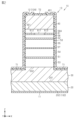
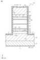
- FIG. 2 is a schematic cross-sectional view showing a layer structure of the surface-emitting laser device of FIG.
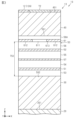
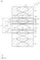
- FIG. 3 is a cross-sectional view showing an example of the layer configuration of the light generating layer and the light reflecting layer of FIG.
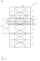
- FIG. 4 is a cross-sectional view showing an example of the relationship between the layer configuration of the light generating layer and the light reflecting layer of FIG. 2 and the wavelength.
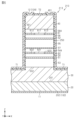
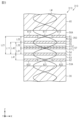
- FIG. 5 is a cross-sectional view showing a modification of the layer configuration of the light generating layer and the light reflecting layer of FIG. 2 and the relationship between wavelength and the layer configuration.
- FIG. 1 is a schematic plan view showing a surface emitting laser device according to the first embodiment.
- FIG. 2 is a schematic cross-sectional view showing a layer structure of the surface-emitting laser device of FIG.
- FIG. 3 is a cross-sectional view showing an example of the layer configuration of the
- FIG. 6 is a schematic cross-sectional view showing a layer structure of the surface-emitting laser device according to the second embodiment.
- FIG. 7 is a cross-sectional view showing an example of the relationship between the layer configuration of the light generating layer and the light reflecting layer shown in FIG. 6 and the wavelength.
- FIG. 8 is a schematic cross-sectional view showing a layer structure of the surface-emitting laser device according to the third embodiment.
- FIG. 9 is a cross-sectional view showing an example of the relationship between the layer configuration of the light generating layer and the light reflecting layer of FIG. 8 and the wavelength.
- At least one means “one or more” of the desired options.
- at least one means “only one option” or “both of two options” if the number of options is two.
- at least one means “only one option” or “any combination of two or more options” if the number of options is three or more.
- FIG. 1 is a schematic plan view showing a surface emitting laser device.
- the surface-emitting laser device 10 is a semiconductor laser device known as a VCSEL (Vertical Cavity Surface Emitting Laser).
- the surface emitting laser device 10 is formed in a roughly rectangular parallelepiped shape.
- the surface-emitting laser device 10 includes an element front surface 101, an element rear surface 102, and a number of element side surfaces 103, 104, 105, and 106.
- the element front surface 101 and the element rear surface 102 face in opposite directions.
- the direction in which the element front surface 101 faces is the thickness direction Z.
- Two axial directions perpendicular to the thickness direction Z and perpendicular to each other are the first direction X and the second direction Y.
- the surface-emitting laser device 10 of the first embodiment is said to be viewed from the thickness direction Z in a plan view.
- the surface-emitting laser device 10 is formed in a rectangular shape whose length in the second direction Y is longer than its length in the first direction X.
- the shape of the surface-emitting laser device 10 in a plan view can be changed arbitrarily.
- the element side surfaces 103 and 104 face in opposite directions in the first direction X.
- the element side surfaces 105 and 106 face in opposite directions in the second direction Y.
- the surface-emitting laser device 10 has a first electrode 11 provided on the rear surface 102 of the element, and a second electrode 12 provided on the front surface 101 of the element.
- the first electrode 11 is, for example, an n-type electrode.
- the second electrode is, for example, a p-type electrode.
- the first electrode 11 can be provided, for example, on the entire rear surface 102 of the element.
- the second electrode 12 is, for example, formed in a rectangular shape in a plan view.
- the second electrode 12 includes electrode portions 12A of the multiple light-emitting portions 13 and a rectangular external connection portion 12C extending along the side surface 106 of the element.
- a conductor such as a bonding wire is connected to the external connection portion 12C.
- An external terminal may be connected to the external connection portion 12C, and a conductor such as a bonding wire may be connected to the external terminal.
- the surface-emitting laser device 10 includes a light-emitting section 13 formed on the element surface 101 and emitting laser light in the thickness direction Z.
- the surface-emitting laser device 10 of the first embodiment includes a plurality of light-emitting sections 13.
- the plurality of light-emitting sections 13 are formed at intervals in the first direction X and the Y direction in a plan view.
- the plurality of light-emitting sections 13 are arranged inside the frame-shaped second electrode 12.
- the plurality of light-emitting sections 13 are arranged at intervals from each other in the first direction X and the second direction Y in a plan view. In one example, the plurality of light-emitting sections 13 are arranged in a staggered manner in a plan view.
- the plurality of light-emitting sections 13 are arranged in a manner in which one light-emitting section 13 is located at each of the three vertices of a triangle (for example, an equilateral triangle) in a plan view. It can also be said that the plurality of light-emitting sections 13 are arranged in a manner in which one light-emitting section 13 is located at each of the six vertices of a hexagon (for example, a regular hexagon) in a plan view.
- the arrangement of the multiple light-emitting units 13 can be any arrangement, such as a matrix, a radial arrangement (concentric circles), etc.
- Fig. 2 is a schematic cross-sectional view showing the layer structure of an exemplary surface-emitting laser device according to the first embodiment, illustrating the layer structure of one light-emitting section 13.
- Fig. 3 is a cross-sectional view showing an example of the layer structure of a light generating layer 50, a first light reflecting layer 30, and a second light reflecting layer 40.
- the surface-emitting laser device 10 includes a substrate 20, a first light reflecting layer 30, a second light reflecting layer 40, and a light generating layer 50.
- the first light reflecting layer 30, the light generating layer 50, and the second light reflecting layer 40 are provided on the substrate 20.
- the first light reflecting layer 30 is provided on the substrate 20 and is in contact with the substrate 20.
- the light generating layer 50 is provided on the first light reflecting layer 30 and is in contact with the first light reflecting layer 30.
- the second light reflecting layer 40 is provided on the light generating layer 50 and is in contact with the light generating layer 50.
- the substrate 20 includes a compound semiconductor material.
- the substrate 20 includes, for example, a single crystal of a compound semiconductor material that forms a tetragonal crystal.
- the compound semiconductor material may be a III-V group semiconductor material.
- the substrate 20 is, for example, made of a GaAs single crystal containing an n-type impurity.
- the n-type impurity may be, for example, Si (silicon).
- the substrate 20 includes a substrate upper surface 201 and a substrate lower surface 202 that face in opposite directions in the thickness direction Z.
- the substrate lower surface 202 constitutes the element rear surface 102.
- the first electrode 11 is provided on the bottom surface 202 of the substrate.
- the first electrode 11 forms an ohmic contact with the bottom surface 202 of the substrate 20.
- the first electrode 11 may include multiple electrode films.
- the first electrode 11 may be composed of one electrode film.
- the first electrode 11 may include, for example, Ni (nickel), Au (gold), Ge (germanium), Ti (titanium), In (indium), Zn (zinc), etc.
- the first electrode 11 is composed of a stack of an AuGe layer, a Ni layer, and an Au layer.
- the second electrode 12 may include multiple electrode films.
- the second electrode 12 may be composed of one electrode film.
- the second electrode 12 may include, for example, Au, Ti, etc.
- the second electrode 12 is composed of a stack of a Ti layer and an Au layer.
- the surface-emitting laser device 10 may include a contact layer interposed between the second light reflecting layer 40 and the second electrode 12.
- the first light reflecting layer 30 and the second light reflecting layer 40 are arranged in the thickness direction Z so as to sandwich the light generating layer 50.
- the first light reflecting layer 30 is provided on the upper surface 201 of the substrate 20.
- the light generating layer 50 is provided on the first light reflecting layer 30.
- the second light reflecting layer 40 is provided on the light generating layer 50.
- the second electrode 12 is provided on the second light reflecting layer 40.
- the second electrode 12 on the second light reflecting layer 40 may be formed, for example, in a ring shape.
- the first light reflecting layer 30 is composed of a first conductivity type DBR (Distributed Bragg Reflector) layer.
- the first conductivity type is, for example, n-type.
- the first light reflecting layer 30 contains impurities of the first conductivity type.
- the impurities of the first conductivity type may be, for example, at least one of Si and Te (tellurium).
- the first light reflecting layer 30 has a refractive index that changes periodically along the thickness direction Z, and resonantly reflects a specific wavelength component.
- the first light reflecting layer 30 has a laminated structure in which a first reflecting layer and a second reflecting layer containing Al are laminated.
- the first reflecting layer and the second reflecting layer have mutually different refractive indices.
- the first light reflecting layer 30 includes a plurality of first reflecting layers and a plurality of second reflecting layers.
- the first reflecting layer may include Al ⁇ 1 Ga (1- ⁇ 1) As having an Al composition ⁇ 1.
- the second reflecting layer may include Al ⁇ 2 Ga (1- ⁇ 2) As having an Al composition ⁇ 2.
- the Al composition ⁇ 1 of the first reflecting layer may be greater than 0 and equal to or less than 0.2.
- the Al composition ⁇ 2 of the second reflecting layer may be equal to or greater than 0.85 and equal to or less than 0.97.
- the reflectance of the reflecting layer containing AlGaAs decreases as the Al composition increases. Therefore, the refractive index of the first reflecting layer and the refractive index of the second reflecting layer are different from each other.
- the second light reflecting layer 40 is composed of a DBR layer of a second conductivity type.
- the second conductivity type is, for example, p-type.
- the second light reflecting layer 40 contains impurities of the second conductivity type.
- the impurities of the second conductivity type may be, for example, at least one of C (carbon), Zn, and Mg (magnesium).
- the second light reflecting layer 40 has a refractive index that changes periodically along the thickness direction Z, and resonantly reflects a specific wavelength component.
- the second light reflecting layer 40 has a laminated structure in which a third reflecting layer and a fourth reflecting layer containing an Al composition are laminated.
- the third reflecting layer and the fourth reflecting layer have different refractive indices.
- the second light reflecting layer 40 of the first embodiment includes a plurality of third reflecting layers and a plurality of fourth reflecting layers.
- the third reflecting layer may include Al ⁇ 3 Ga (1- ⁇ 3) As having an Al composition ⁇ 3.
- the fourth reflecting layer may include Al ⁇ 4 Ga (1- ⁇ 4) As having an Al composition ⁇ 4.
- the Al composition ⁇ 3 of the third reflecting layer may be 0.85 or more and 0.97 or less.
- Each light-emitting section 13 of the surface-emitting laser device 10 emits laser light of a specific wavelength component that is reflected by the first light-reflecting layer 30 and the second light-reflecting layer 40 of each light-emitting section 13.
- the wavelength of the laser light is ⁇ . It can be said that each light-emitting section 13 generates laser light of wavelength ⁇ by the first light-reflecting layer 30 and the second light-reflecting layer 40.
- the light generating layer 50 includes a first active layer 51 and a second active layer 52.
- the first active layer 51 and the second active layer 52 are arranged in the thickness direction Z, that is, from the first light reflecting layer 30 toward the second light reflecting layer 40, in that order.
- the first active layer 51 and the second active layer 52 may have a QW (Quantum Well) structure including a quantum well layer and a barrier layer.
- the first active layer 51 and the second active layer 52 may have an MQW (Multi Quantum Well) structure in which quantum well layers and barrier layers are alternately stacked at any period.
- the quantum well layer may include GaAs, AlGaAs, or InGaAs.
- the quantum well layer may be free of impurities.
- the barrier layer has a band gap larger than the band gap of the quantum well layer.
- the cladding layers 53 and 54 are arranged to sandwich the first active layer 51.
- the cladding layers 55 and 56 are arranged to sandwich the second active layer 52.
- the cladding layers 53 and 55 arranged on the first light reflecting layer 30 side with respect to the active layers 51 and 52 are first cladding layers containing a first conductivity type impurity.
- the first conductivity type impurity may be, for example, Si.
- the first cladding layers 53 and 55 contain Al C Ga (1-C) As having an Al composition C.
- the Al composition C may be 0.2 or more and 0.8 or less.
- the cladding layers 54 and 56 arranged on the second light reflecting layer 40 side with respect to the active layers 51 and 52 are second cladding layers containing a second conductivity type impurity.
- the second conductivity type impurity may be, for example, C.
- the second cladding layers 54 and 56 contain Al C Ga (1-C) As having an Al composition C.
- the light generating layer 50 includes a tunnel junction layer 57.
- the tunnel junction layer 57 is disposed between adjacent cladding layers in the thickness direction Z in which the active layers 51 and 52 are disposed, that is, between the second cladding layer 54 and the first cladding layer 55.
- the tunnel junction layer 57 passes a tunnel current due to the tunnel effect.
- the surface-emitting laser device 10 includes a current confinement layer 61.
- the current confinement layer 61 may be disposed between the first electrode 11 and the second electrode 12.
- the current confinement layer 61 is provided between the second active layer 52 and the second electrode 12.
- the current confinement layer 61 is disposed between the second cladding layer 56, which sandwiches the second active layer 52, and the second optical reflection layer 40.
- An adjustment layer 56A is provided between the current confinement layer 61 and the second optical reflection layer 40.
- the adjustment layer 56A adjusts the position of the current confinement layer 61.
- the adjustment layer 56A has the same composition as the second cladding layer 56, for example.
- the current confinement layer 61 constricts the current supplied to the active layers 51 and 52.
- the current confinement layer 61 includes a current passing portion 611 and a current confinement portion 612.
- the current passing portion 611 may be formed of a material containing Al.
- the current passing portion 611 is configured of a material containing AlAs (Al x Ga (1-x) As, where the Al composition x is 0.95 or more and 1.00 or less).
- the current passing portion 611 may contain an impurity of the second conductivity type.
- This current passing portion 611 is provided in the inner portion of each light emitting portion 13. For example, in a plan view, the current passing portion 611 is disposed in the center of each light emitting portion 13. For example, the current passing portion 611 is formed in a circular shape in a plan view.
- the current confinement portion 612 has insulating properties.
- the current confinement portion 612 is composed of an oxide layer.
- the current confinement portion 612 includes an oxide layer containing Al.
- the oxide layer containing Al is, for example, Al 2 O 3 (alumina).
- the oxide layer may contain Ga or As.
- the current confinement portion 612 is disposed on the side of the side of each light emitting portion 13 with respect to the current passing portion 611.
- the current confinement portion 612 is formed in a ring shape (for example, a circular ring shape) surrounding the current passing portion 611.
- the current confinement portion 612 is formed by oxidizing the periphery of a layer containing AlAs.
- the film thickness (physical thickness) of the current confinement layer 61 can be, for example, 15 nm or more and 100 nm or less.
- the current confinement layer 61 includes an opening 613 formed by a ring-shaped current confinement portion 612.
- the opening 613 is formed in an arc shape with the center of the current confinement portion 612 in the thickness direction Z expanding toward the current passing portion 611.
- This current confinement portion 612 constricts the current flowing between the first electrode 11 and the second electrode 12 in each light-emitting portion 13.
- the current flowing between the first electrode 11 and the second electrode 12 passes through the current passing portion 611 inside the opening 613.
- the region of the first active layer 51 and the region of the second active layer 52 facing this current passing portion 611 become the light-emitting region.
- the current confinement layer 61 increases the current density in the active layers 51 and 52. This improves the luminous efficiency of the light generated in the active layers 51 and 52.
- the surface-emitting laser device 10 includes an insulating film 71 that covers the light-emitting section 13.
- the insulating film 71 is formed to cover the surface of the first light-reflecting layer 30, the side surface of the light-generating layer 50, and the side surface of the second light-reflecting layer 40.
- the insulating film 71 may include, for example, silicon oxide such as SiO 2 or SiO, SiN (silicon nitride), SiON, ZrO 2 (zirconium oxide), or TiO (titanium oxide).
- the insulating film 71 includes a covering section 72 that covers the upper surface of the second light-reflecting layer 40 in each light-emitting section 13.
- the covering section 72 covers the upper surface of the second light-reflecting layer 40 exposed from the second electrode 12.
- FIG. 4 is a cross-sectional view showing an example of the relationship between the layer configuration of the light generating layer 50 constituting the light emitting section 13 and the waveform of the laser light LW.
- the laser light LW shown in FIG. 4 is the waveform of the laser light LW, and indicates the electric field intensity. Note that the waveform of the laser light LW in FIG. 4 is shown to have a constant length for the wavelength ⁇ .
- the light generating layer 50 includes a first active layer 51 and a second active layer 52.
- the optical distance L11 between the first active layer 51 and the second active layer 52 is preferably ⁇ k1/2 (k1 is a natural number).
- the optical distance L11 between the first active layer 51 and the second active layer 52 is ⁇ /2.
- the first active layer 51 and the second active layer 52 are located at the antinode positions of the laser light LW having a wavelength ⁇ by the first light reflecting layer 30 and the second light reflecting layer 40.
- the current confinement layer 61 is disposed at a position different from the antinode position of the laser light LW generated by the first light reflection layer 30, the second light reflection layer 40, and the active layers 51 and 52.
- the current confinement layer 61 is preferably disposed at an optical distance of ⁇ (2 ⁇ k3-1)/4 (k3 is a natural number) away from the active layers 51 and 52.
- the light emitting section 13 of the first embodiment includes two active layers 51 and 52 and one current confinement layer 61.
- the optical distance L21 between the current confinement layer 61 and the first active layer 51 close to the first light reflection layer 30 is ⁇ 3/4.
- the current confinement layer 61 is located at an optical distance of ⁇ 3/4 from the first active layer 51 close to the first light reflection layer 30.
- the optical distance L22 between the current confinement layer 61 and the second active layer 52 close to the second light reflection layer 40 is ⁇ /4.
- the current confinement layer 61 is located at an optical distance of ⁇ /4 from the second active layer 52 close to the second light reflection layer 40.
- the active layers 51 and 52 are located at the antinode positions of the laser light LW in the light emitting section 13.
- the current confinement layer 61 is located at the node position of the laser light LW.
- the antinode positions of the laser light LW are positions where the electric field strength is high, and the node positions are positions where the electric field strength is low.
- the difference between the current confinement layer 61 and a position that is an optical distance ⁇ (2 ⁇ k3-1)/4 (k3 is a natural number) away from the first active layer 51 is, for example, ⁇ /8 or less, then the current confinement layer 61 can be said to be located at a position that is an optical distance ⁇ (2 ⁇ k3-1)/4 (k3 is a natural number) away from the active layers 51 and 52, and can be said to be located at a node position.
- the tunnel junction layer 57 is disposed at a position with respect to the laser light LW that is different from the antinode position of the laser light LW.
- the tunnel junction layer 57 is preferably disposed at a position that is an optical distance ⁇ (2 ⁇ k2-1)/4 (k2 is a natural number) away from the active layers 51, 52.
- the tunnel junction layer 57 is disposed at a position in the thickness direction of the tunnel junction layer 57 where a predetermined position inside the tunnel junction layer 57 is an optical distance ⁇ (2 ⁇ k2-1)/4 (k2 is a natural number) away from the active layers 51, 52. It can be said that the tunnel junction layer 57 is disposed at a node position of the laser light LW.
- the tunnel junction layer 57 can be said to be located at a position that is an optical distance ⁇ (2 ⁇ k2-1)/4 (k2 is a natural number) away from the active layers 51 and 52, and can be said to be located at a nodal position.
- the tunnel junction layer 57 includes a first tunnel layer 571 of a first conductivity type and a second tunnel layer 572 of a second conductivity type.
- the second tunnel layer 572 is disposed on the second light reflecting layer 40 side of the first tunnel layer 571.
- the first tunnel layer 571 and the second tunnel layer 572 are in contact with each other.
- the first tunnel layer 571 is in contact with the second cladding layer 54.
- the second tunnel layer 572 is in contact with the first cladding layer 55.
- the first tunnel layer 571 includes an impurity of a first conductivity type.
- the first tunnel layer 571 is doped with a high concentration of an impurity of the first conductivity type.
- the impurity concentration in the first tunnel layer 571 may be, for example, 5 ⁇ 10 18 cm ⁇ 3 or more and 5 ⁇ 10 20 cm ⁇ 3 or less.
- the second tunnel layer 572 includes an impurity of a second conductivity type.
- the second tunnel layer 572 is doped with a high concentration of an impurity of the second conductivity type.
- the impurity concentration in the second tunnel layer 572 may be, for example, 5 ⁇ 10 18 cm ⁇ 3 or more and 5 ⁇ 10 20 cm ⁇ 3 or less.
- the film thickness of the first tunnel layer 571 may be, for example, 10 nm or more and 30 nm or less.
- the film thickness of the second tunnel layer 572 may be, for example, 10 nm or more and 30 nm or less.
- the optical distance L31 between the first tunnel layer 571 and the first active layer 51 is ⁇ /4.
- the first tunnel layer 571 is disposed at a position that is an optical distance of ⁇ /4 away from the first active layer 51.
- the first tunnel layer 571 is disposed at a position in the thickness direction of the first tunnel layer 571 such that the center of the first tunnel layer 571 is an optical distance of ⁇ (2 ⁇ k2-1)/4 (k2 is a natural number) away from the first active layer 51.
- the first tunnel layer 571 is disposed at a node position of the laser light LW.
- the first tunnel layer 571 can be said to be located at a position that is an optical distance ⁇ (2 ⁇ k2-1)/4 (k2 is a natural number) away from the active layers 51 and 52, and can be said to be located at a node position.
- the optical distance L32 between the first tunnel layer 571 and the second active layer 52 is ⁇ /4.
- the first tunnel layer 571 is disposed at a position that is an optical distance of ⁇ /4 away from the second active layer 52.
- the first tunnel layer 571 is disposed at a position in the thickness direction of the first tunnel layer 571 such that the center of the first tunnel layer 571 is an optical distance of ⁇ (2 ⁇ k2-1)/4 (k2 is a natural number) away from the second active layer 52.
- the first tunnel layer 571 is disposed at a node position of the laser light LW.
- the surface-emitting laser device 10 includes a light generating layer 50, a first light reflecting layer 30 of a first conductivity type, and a second light reflecting layer 40 of a second conductivity type, which are arranged to sandwich the light generating layer 50.
- the light generating layer 50 includes active layers 51 and 52, first cladding layers 53 and 55, second cladding layers 54 and 56, and a tunnel junction layer 57.
- the active layers 51 and 52 are arranged between the first light reflecting layer 30 and the second light reflecting layer 40 in a direction from the first light reflecting layer 30 to the second light reflecting layer 40.
- the first cladding layers 53 and 55 are arranged on the first light reflecting layer 30 side with respect to the active layers 51 and 52, respectively.
- the second cladding layers 54 and 56 are arranged on the second light reflecting layer 40 side with respect to the active layers 51 and 52, respectively.
- the tunnel junction layer 57 is disposed between the second cladding layer 54 and the first cladding layer 55 between two adjacent active layers 51, 52 in the direction from the first light reflecting layer 30 toward the second light reflecting layer 40. Furthermore, when the wavelength of the laser light LW is ⁇ , the tunnel junction layer 57 is disposed at an optical distance ⁇ (2 ⁇ k2 ⁇ 1)/4 (k2 is a natural number) away from the active layers 51, 52.
- the tunnel junction layer 57 has a higher impurity concentration than the cladding layers 53 to 56. Such a tunnel junction layer 57 is more likely to absorb the laser light LW generated by the active layers 51 and 52 than the cladding layers 53 to 56. Therefore, the tunnel junction layer 57 can cause a loss in the optical intensity of the laser light LW generated by the light emitting unit 13. The higher the electric field intensity of the laser light LW that becomes a standing wave, the greater the loss. Therefore, by arranging the tunnel junction layer 57 at a position different from the antinode position of the laser light LW, the loss of the laser light LW caused by the tunnel junction layer 57 can be reduced.
- the loss in the laser light LW can be further reduced.
- the active layers 51 and 52 are antinode positions where the electric field strength is highest in the waveform of the laser light LW. Therefore, by locating the tunnel junction layer 57 at an optical distance of ⁇ (2 ⁇ k2-1)/4 (k2 is a natural number) away from the active layers 51 and 52, the loss of the laser light LW due to the tunnel junction layer 57 can be further reduced.
- the tunnel junction layer 57 includes a first tunnel layer 571 of a first conductivity type and a second tunnel layer 572 of a second conductivity type. Therefore, the first tunnel layer 571 is more likely to absorb the laser light LW than the second tunnel layer 572. Therefore, by arranging the first tunnel layer 571 at an optical distance ⁇ (2 ⁇ k2-1)/4 (k2 is a natural number) away from the active layers 51 and 52, the loss of the laser light LW due to the tunnel junction layer 57 can be further reduced.
- the surface-emitting laser device 10 of the first embodiment includes a current confinement layer 61 disposed between the second active layer 52 and the second electrode 12 .
- the current confinement layer 61 includes a current confinement portion 612 that forms an opening 613, and a current passing portion 611 that is disposed inside the opening 613.
- the current passing portion 611 is formed of a material that includes AlAs.
- the second cladding layer 56 between the second active layer 52 and the second light reflecting layer 40 includes Al 2 A 2 Ga (1-A 2) As having an Al composition A2. Therefore, it can be said that the current passing portion 611 has an Al composition higher than the Al composition A2 of the second cladding layer 56.
- the impurity concentration of the second conductive type impurity (for example, C, Zn, Mg) is increased to reduce the resistance. Therefore, in the current passing portion 611, similar to the tunnel junction layer 57, the laser light LW is more easily absorbed than the cladding layers 53 to 56. Therefore, the current confinement layer 61 can cause a loss in the light intensity of the laser light LW generated by the light emitting portion 13. In the laser light LW, the higher the electric field intensity of the laser light LW that becomes a standing wave, the greater the loss. Therefore, by disposing the current confinement layer 61 at a position different from the antinode position of the laser light LW, the loss of the laser light LW due to the current confinement layer 61 can be reduced.
- the second conductive type impurity for example, C, Zn, Mg
- the current confinement layer 61 is disposed at an optical distance of ⁇ (2 ⁇ k3-1)/4 (k3 is a natural number) away from the active layers 51, 52. Therefore, the current confinement layer 61 is disposed at a node position in the laser light LW, that is, at a position where the electric field strength is low. This makes it possible to further reduce the loss of the laser light LW due to the current confinement layer 61.
- the surface emitting laser device 10 provides the following advantages.
- (1-1) Surface-emitting laser device 10 includes a light generating layer 50, and a first light reflecting layer 30 of a first conductivity type and a second light reflecting layer 40 of a second conductivity type arranged to sandwich light generating layer 50.
- Light generating layer 50 includes active layers 51 and 52, first cladding layers 53 and 55, second cladding layers 54 and 56, and a tunnel junction layer 57. Therefore, the light intensity of laser light LW emitted from surface-emitting laser device 10 can be improved compared to a surface-emitting laser device including a single active layer in the light generating layer of the light-emitting section.
- the active layers 51 and 52 are arranged between the first light reflecting layer 30 and the second light reflecting layer 40 in a direction from the first light reflecting layer 30 to the second light reflecting layer 40.
- the first cladding layers 53 and 55 are arranged on the first light reflecting layer 30 side with respect to the active layers 51 and 52, respectively.
- the second cladding layers 54 and 56 are arranged on the second light reflecting layer 40 side with respect to the active layers 51 and 52, respectively.
- the tunnel junction layer 57 is arranged between the second cladding layer 54 and the first cladding layer 55 between the two adjacent active layers 51 and 52 in a direction from the first light reflecting layer 30 to the second light reflecting layer 40. Furthermore, the tunnel junction layer 57 is arranged at an optical distance of ⁇ (2 ⁇ k2-1)/4 (k2 is a natural number) from the active layers 51 and 52, where ⁇ is the wavelength of the laser light LW.
- the loss in the laser light LW can be further reduced.
- the active layers 51 and 52 are antinode positions where the electric field strength is highest in the waveform of the laser light LW. Therefore, by locating the tunnel junction layer 57 at an optical distance of ⁇ (2 ⁇ k2-1)/4 (k2 is a natural number) away from the active layers 51 and 52, the loss of the laser light LW due to the tunnel junction layer 57 can be further reduced.
- the tunnel junction layer 57 includes a first tunnel layer 571 of a first conductivity type and a second tunnel layer 572 of a second conductivity type. Therefore, the first tunnel layer 571 is more likely to absorb the laser light LW than the second tunnel layer 572. Therefore, by arranging the first tunnel layer 571 at an optical distance ⁇ (2 ⁇ k2-1)/4 (k2 is a natural number) away from the active layers 51 and 52, the loss of the laser light LW due to the tunnel junction layer 57 can be further reduced.
- the surface-emitting laser device 10 of the first embodiment includes a current confinement layer 61 disposed between the second active layer 52 and the second electrode 12.
- the current confinement layer 61 includes a current confinement portion 612 forming an opening 613, and a current passing portion 611 disposed inside the opening 613.
- the current passing portion 611 is formed of a material containing AlAs.
- the second cladding layer 56 between the second active layer 52 and the second light reflecting layer 40 contains Al A2 Ga (1-A2) As having an Al composition A2. Therefore, it can be said that the current passing portion 611 has an Al composition higher than the Al composition A2 of the second cladding layer 56.
- the impurity concentration of the second conductive type impurity (for example, C, Zn, Mg) is increased to reduce the resistance. Therefore, like the tunnel junction layer 57, the current passing portion 611 is more likely to absorb the laser light LW than the cladding layers 53 to 56. Therefore, the current confinement layer 61 can cause a loss in the light intensity of the laser light LW generated by the light emitting portion 13. The higher the electric field intensity of the laser light LW that becomes a standing wave, the greater the loss. Therefore, by arranging the current confinement layer 61 at a position different from the antinode position of the laser light LW, the loss of the laser light LW caused by the current confinement layer 61 can be reduced.
- the second conductive type impurity for example, C, Zn, Mg
- the current confinement layer 61 is disposed at an optical distance of ⁇ (2 ⁇ k3-1)/4 (k3 is a natural number) away from the active layers 51, 52. Therefore, the current confinement layer 61 is disposed at a node position in the laser light LW, that is, at a position where the electric field strength is low. This makes it possible to further reduce the loss of the laser light LW due to the current confinement layer 61.
- (Modification of the first embodiment) 5 is a schematic cross-sectional view showing a layer structure of a surface-emitting laser device 10A according to a modified example.
- the surface-emitting laser device 10A according to this modified example is different from the surface-emitting laser device 10 according to the first embodiment in the optical distance L31 between the tunnel junction layer 57 and the first active layer 51. For this reason, the same reference numerals as those of the surface-emitting laser device 10 according to the first embodiment are used.
- the light generating layer 50A of the light emitting section 13A includes a first active layer 51 and a second active layer 52.
- the optical distance L11 between the first active layer 51 and the second active layer 52 is preferably ⁇ k1/2 (k1 is a natural number).
- the optical distance L11 between the first active layer 51 and the second active layer 52 is ⁇ .
- the first active layer 51 and the second active layer 52 are located at the antinode positions of the laser light LW.
- the optical distance L32 between the tunnel junction layer 57 and the second active layer 52 is ⁇ /4, as in the first embodiment described above.
- the optical distance L31 between the tunnel junction layer 57 and the first active layer 51 is ⁇ 3/4.
- the optical distance L31 between the tunnel junction layer 57 and the first active layer 51 is shown.
- the optical distance L32 between the tunnel junction layer 57 and the second active layer 52 may be changed.
- the optical distance L31 between the tunnel junction layer 57 and the first active layer 51, and the optical distance L32 between the tunnel junction layer 57 and the second active layer 52 may be changed.
- the optical distance L22 between the second active layer 52 and the current confinement layer 61 may be changed.
- Fig. 6 is a schematic cross-sectional view showing the layer structure of an exemplary surface-emitting laser device 210 according to the second embodiment, showing the layer structure of one light-emitting section 213.
- Fig. 7 is a cross-sectional view showing an example of the relationship between the layer structure of the light-generating layer 250 constituting the light-emitting section 213 of the surface-emitting laser device 210 in Fig. 6 and the waveform of the laser light LW.
- the same components as those in the surface-emitting laser device 10 according to the first embodiment are denoted by the same reference numerals. In the following, the description of the same components as those in the first embodiment will be omitted, and components different from those in the first embodiment will be described.
- the surface emitting laser device 210 of the second embodiment includes two current confinement layers 61 and 62 .
- the first current confinement layer 61 is disposed between the second active layer 52 and the second electrode 12 (12A). In one example, the first current confinement layer 61 is disposed between the second active layer 52 and the second light reflecting layer 40.
- the second current confinement layer 62 can be disposed between the first active layer 51 and the second electrode 12 (12A). In one example, the second current confinement layer 62 can be disposed between the first active layer 51 and the second active layer 52. In the surface-emitting laser device 210 shown in FIG. 6, the second current confinement layer 62 is disposed between the first active layer 51 and the tunnel junction layer 57. That is, in the surface-emitting laser device 210 of the second embodiment, the current confinement layers 62, 61 are disposed on the second electrode 12 (12A) side with respect to each of the active layers 51, 52. Between the second current confinement layer 62 and the tunnel junction layer 57, an adjustment layer 54A is interposed. The adjustment layer 54A has the same composition as the second cladding layer 54, for example.
- the first current confinement layer 61 includes a first current passing portion 611 and a first current confinement portion 612.
- the first current passing portion 611 may be formed of a material containing Al.
- the first current passing portion 611 is configured of a material containing AlAs (Al x1 Ga (1-x1) As, where the Al composition x1 is 0.95 or more and 1.00 or less).
- the first current passing portion 611 may contain an impurity of the second conductivity type.
- This first current passing portion 611 is provided in the inner portion of each light emitting portion 13. For example, in a plan view, the first current passing portion 611 is disposed in the center of each light emitting portion 13. For example, the first current passing portion 611 is formed in a circular shape in a plan view.
- the first current confinement portion 612 has insulating properties.
- the first current confinement portion 612 includes an oxide layer containing Al.
- the oxide layer containing Al is, for example, Al 2 O 3.
- the oxide layer may contain Ga or As.
- the first current confinement portion 612 is disposed on the side of the side of each light emitting portion 13 with respect to the first current passing portion 611.
- the first current confinement portion 612 is formed in a ring shape (for example, a circular ring shape) surrounding the first current passing portion 611.
- the first current confinement portion 612 is formed by oxidizing the periphery of a layer containing AlAs.
- the film thickness (physical thickness) of the first current confinement layer 61 can be, for example, 15 nm or more and 100 nm or less.
- the first current confinement layer 61 includes a first opening 613 formed by a ring-shaped first current confinement portion 612.
- the first opening 613 is formed in an arc shape in which the center of the thickness direction Z of the first current confinement portion 612 bulges toward the first current passing portion 611.
- This first current confinement portion 612 constricts the current flowing between the first electrode 11 and the second electrode 12 in each light-emitting portion 13.
- the current flowing between the first electrode 11 and the second electrode 12 passes through the first current passing portion 611 inside the first opening 613.
- the region of the second active layer 52 facing this first current passing portion 611 becomes the light-emitting region.
- the first current confinement layer 61 increases the current density in the active layer 52. This improves the luminous efficiency of the light generated in the active layer 52.
- the second current confinement layer 62 includes a second current passing portion 621 and a second current confinement portion 622.
- the second current passing portion 621 may be formed of a material containing Al.
- the second current passing portion 621 is composed of a material containing AlAs (Al x2 Ga (1-x2) As, where the Al composition x2 is 0.95 or more and 1.00 or less).
- the second current passing portion 621 may contain an impurity of the second conductivity type.
- This second current passing portion 621 is provided in the inner portion of each light emitting portion 13. For example, in a plan view, the second current passing portion 621 is disposed in the center of each light emitting portion 13. For example, the second current passing portion 621 is formed in a circular shape in a plan view.
- the second current confinement portion 622 has insulating properties.
- the second current confinement portion 622 is composed of an oxide layer.
- the second current confinement portion 622 includes an oxide layer containing Al.
- the oxide layer containing Al is, for example, Al 2 O 3.
- the oxide layer may contain Ga or As.
- the second current confinement portion 622 is disposed on the side of the side of each light emitting portion 13 with respect to the second current passing portion 621.
- the second current confinement portion 622 is formed in a ring shape (for example, a circular ring shape) surrounding the second current passing portion 621.
- the second current confinement portion 622 is formed by oxidizing the periphery of a layer containing AlAs.
- the film thickness (physical thickness) of the second current confinement layer 62 can be, for example, 15 nm or more and 100 nm or less.
- the second current confinement layer 62 includes a second opening 623 formed by a ring-shaped second current confinement portion 622.
- the second opening 623 is formed in an arc shape in which the center of the thickness direction Z of the second current confinement portion 622 bulges toward the second current passing portion 621.
- This second current confinement portion 622 constricts the current flowing between the first electrode 11 and the second electrode 12 in each light-emitting portion 13.
- the current flowing between the first electrode 11 and the second electrode 12 passes through the second current passing portion 621 inside the second opening 623.
- the region of the first active layer 51 facing this second current passing portion 621 becomes the light-emitting region.
- the second current confinement layer 62 increases the current density in the first active layer 51. This improves the luminous efficiency of the light generated in the first active layer 51.
- the laser light LW shown in Fig. 7 is a waveform of the laser light LW, and indicates the electric field intensity. Note that the waveform of the laser light LW in Fig. 7 is shown to have a constant length with respect to the wavelength ⁇ .
- the light emitting section 213 includes a first active layer 51 and a second active layer 52.
- the optical distance L11 between the first active layer 51 and the second active layer 52 is preferably ⁇ k1/2 (k1 is a natural number).
- the optical distance L11 between the first active layer 51 and the second active layer 52 is ⁇ .
- the first active layer 51 and the second active layer 52 are located at the antinode positions of the laser light LW.
- the first current confinement layer 61 is disposed at a position with respect to the laser light LW that is different from the antinode position of the laser light LW.
- the first current confinement layer 61 is preferably disposed at a position that is an optical distance ⁇ (2 ⁇ k3-1)/4 (k3 is a natural number) away from the active layers 51, 52.
- the optical distance L22 between the first current confinement layer 61 and the second active layer 52 close to the second optical reflection layer 40 is ⁇ /4.
- the optical distance L21 between the first current confinement layer 61 and the first active layer 51 close to the first optical reflection layer 30 is ⁇ 5/4.
- the first current confinement layer 61 can be said to be located at a position that is an optical distance ⁇ (2 ⁇ k3-1)/4 (k3 is a natural number) away from the active layers 51, 52, and can be said to be located at a node position.
- the second current confinement layer 62 is disposed at a position with respect to the laser light LW that is different from the antinode position of the laser light LW.
- the second current confinement layer 62 is preferably disposed at a position that is an optical distance ⁇ (2 ⁇ k3-1)/4 (k3 is a natural number) away from the active layers 51, 52.
- the optical distance L42 between the second current confinement layer 62 and the second active layer 52 close to the second optical reflection layer 40 is ⁇ 3/4.
- the optical distance L41 between the second current confinement layer 62 and the first active layer 51 close to the first optical reflection layer 30 is ⁇ /4.
- the second current confinement layer 62 can be said to be located at a position that is an optical distance ⁇ (2 ⁇ k3-1)/4 (k3 is a natural number) away from the active layers 51, 52, and can be said to be located at a node position.
- the optical distance L32 between the tunnel junction layer 57 and the second active layer 52 is ⁇ /4, as in the first embodiment.
- the optical distance L31 between the tunnel junction layer 57 and the first active layer 51 is ⁇ 3/4.
- the surface emitting laser device 210 of the second embodiment has the following advantages.
- the surface-emitting laser device 210 of the second embodiment has the same effects as the surface-emitting laser device 10 of the first embodiment.
- the light generating layer 250 of the light emitting section 213 includes current confinement layers 62, 61 arranged on the second electrode 12 (12A) side with respect to the active layers 51, 52, respectively.
- the first current confinement layer 61 includes a first current passing portion 611 and a first current confinement portion 612.
- the region of the second active layer 52 facing the first current passing portion 611 becomes the light emitting region.
- the second current confinement layer 62 includes a second current passing portion 621 and a second current confinement portion 622.
- the region of the first active layer 51 facing the second current passing portion 621 becomes the light emitting region.
- the current density in the active layers 51, 52 can be increased by the current confinement layers 62, 61 arranged with respect to the active layers 51, 52, respectively, and therefore the light emission efficiency of the active layers 51, 52 can be improved.
- Fig. 8 is a schematic cross-sectional view showing the layer structure of an exemplary surface-emitting laser device 310 according to the third embodiment, showing the layer structure of one light-emitting section 313.
- Fig. 9 is a cross-sectional view showing an example of the relationship between the layer structure of the light-generating layer 350 constituting the light-emitting section 313 of the surface-emitting laser device 310 of Fig. 8 and the waveform of the laser light LW.
- the same components as those in the surface-emitting laser device 210 according to the second embodiment are denoted by the same reference numerals. In the following, the description of the same components as those in the second embodiment will be omitted, and components different from those in the second embodiment will be described.
- the surface emitting laser device 310 of the third embodiment includes two current confinement layers 61 and 62 .
- the first current confinement layer 61 is disposed between the second active layer 52 and the second light reflecting layer 40 .
- the second current confinement layer 62 can be disposed between the first active layer 51 and the second electrode 12 (12A).
- the second current confinement layer 62 is disposed between the first optical reflection layer 30 and the first active layer 51.
- An adjustment layer 53A is interposed between the second current confinement layer 62 and the first optical reflection layer 30.
- the adjustment layer 53A has the same composition as the first cladding layer 53, for example.
- the laser light LW shown in Fig. 9 is a waveform of the laser light LW, and indicates the electric field intensity. Note that the waveform of the laser light LW in Fig. 9 is shown to have a constant length with respect to the wavelength ⁇ .
- the optical distance L11 between the first active layer 51 and the second active layer 52 is ⁇ /2.
- the optical distance L22 between the first current confinement layer 61 and the second active layer 52 close to the second optical reflection layer 40 is ⁇ /4.
- the optical distance L21 between the first current confinement layer 61 and the first active layer 51 close to the first optical reflection layer 30 is ⁇ 3/4.
- the optical distance L42 between the second current confinement layer 62 and the second active layer 52 close to the second light reflecting layer 40 is ⁇ 3/4.
- the optical distance L41 between the second current confinement layer 62 and the first active layer 51 close to the first light reflecting layer 30 is ⁇ /4.
- the optical distance L32 between the tunnel junction layer 57 and the second active layer 52 is ⁇ /4, as in the first embodiment.
- the optical distance L31 between the tunnel junction layer 57 and the first active layer 51 is ⁇ /4.
- the surface-emitting laser device 310 of the third embodiment has the same effects as the surface-emitting laser device 210 of the second embodiment.
- the number of active layers included in the light generating layer 50 can be three or more.
- the tunnel junction layer 57 is disposed between two adjacent active layers in the thickness direction Z and between the adjacent second cladding layer and first cladding layer.
- the number of the light-emitting portions 13 may be any number equal to or greater than 1.
- the shape of the second electrode 12 shown in Fig. 1 may be appropriately changed depending on the number, arrangement, etc. of the light-emitting portions 13.
- the term “on” as used in this disclosure includes both the meanings of "on” and “above” unless the context clearly indicates otherwise.
- the phrase “a first layer is formed on a second layer” is intended to mean that in some embodiments, the first layer may be disposed directly on the second layer in contact with the second layer, while in other embodiments, the first layer may be disposed above the second layer without contacting the second layer. That is, the term “on” does not exclude a structure in which another layer is formed between the first and second layers.
- the current confinement layer 61 may be located at an optical distance of ⁇ (2 ⁇ k2-1)/4 (k2 is a natural number) from the active layers 51 and 52, and may be located, for example, within the second light reflecting layer 40. Similarly, the current confinement layer 62 may be located within the first light reflecting layer 30.
- the Z-axis direction used in this disclosure does not necessarily have to be vertical, nor does it have to be perfectly aligned with the vertical direction. Therefore, various structures according to this disclosure (for example, the structure shown in FIG. 1) are not limited to the "up” and “down” in the Z-axis direction described in this specification being "up” and “down” in the vertical direction.
- the X-axis direction may be vertical, or the Y-axis direction may be vertical.
- the light generating layer (50, 250, 350) comprises: A plurality of active layers (51, 52) arranged in a direction from the first light reflecting layer (30) to the second light reflecting layer (40) between the first light reflecting layer (30) and the second light reflecting layer (40); a first cladding layer (53, 55) of the first conductivity type (n-type) arranged on the first light reflecting layer (30) side with respect to each of the plurality of active layers (51, 52); a second cladding layer (54, 56) of the second conductivity type (p-type) arranged on the second light reflecting layer (40) side with respect to each of the plurality of active layers (51, 52); a tunnel junction layer (57)
- the tunnel junction layer (57) is A first tunnel layer (571) of the first conductivity type (n-type); A second tunnel layer (572) of the second conductivity type (p-type) arranged on the second light reflecting layer (40) side with respect to the first tunnel layer (571); Including, The first tunnel layer (571) is disposed at an optical distance of ⁇ (2 ⁇ k2 ⁇ 1)/4 (k2 is a natural number) away from the plurality of active layers (51, 52). 2.
- the surface-emitting laser device is A first tunnel layer (571) of the first conductivity type (n-type); A second tunnel layer (572) of the second conductivity type (p-type) arranged on the second light reflecting layer (40) side with respect to the first tunnel layer (571); Including, The first tunnel layer (571) is disposed at an optical distance of ⁇ (2 ⁇ k2 ⁇ 1)/4 (k2 is a natural number) away from the plurality of active layers (51, 52). 2.
- the surface-emitting laser device according to claim 1.
- the surface-emitting laser device according to claim 1 or 2.
- the current confinement layer (61, 62) includes a current confinement portion (612, 622) having the opening (613, 623) and a current passing portion (611, 621) in the opening (613, 623). 4.
- the current confinement layer (61) is disposed between the active layer (52) among the plurality of active layers (51, 52) that is closest to the second light reflecting layer (40) and the second electrode (12); 5.
- the plurality of current confinement layers (61, 62) are a first current confinement layer (61) disposed between the active layer (52) among the plurality of active layers (51, 52) that is closest to the second light reflecting layer (40) and the second electrode (12); a second current confinement layer (62) disposed between the first light reflecting layer (30) and an active layer (51) closest to the first light reflecting layer (30) among the plurality of active layers (51, 52); including, 7.
- the light generating layer (50, 250, 350) comprises: A plurality of active layers (51, 52) arranged in a direction from the first light reflecting layer (30) to the second light reflecting layer (40) between the first light reflecting layer (30) and the second light reflecting layer (40); a first cladding layer (53, 55) of the first conductivity type (n-type) arranged on the first light reflecting layer (30) side with respect to each
- the current confinement layer (61, 62) includes a current confinement portion (612, 622) having the opening (613, 623) and a current passing portion (611, 621) in the opening (613, 623). 10.
- the current confinement layer (61) is disposed between the active layer (52) among the plurality of active layers (51, 52) that is closest to the second light reflecting layer (40) and the second electrode (12); 11.
- the plurality of current confinement layers (61, 62) are a first current confinement layer (61) disposed between the second electrode (12) and an active layer (52) among the plurality of active layers (51, 52) that is closest to the second light reflecting layer (40); a second current confinement layer (62) disposed between the first light reflecting layer (30) and an active layer (51) among the plurality of active layers (51, 52) that is closest to the first light reflecting layer (30); including, 13.
- the first light reflecting layer (30) contains a material containing at least one of Si and Te as an impurity. 16. The surface-emitting laser device according to claim 1 .
- the first cladding layer (53, 55) and the second cladding layer (54, 56) contain Al C Ga (1-C) As having an Al composition of C;
- the Al composition C is 0.2 or more and 0.8 or less.
Landscapes
- Physics & Mathematics (AREA)
- Condensed Matter Physics & Semiconductors (AREA)
- General Physics & Mathematics (AREA)
- Electromagnetism (AREA)
- Optics & Photonics (AREA)
- Semiconductor Lasers (AREA)
Priority Applications (1)
| Application Number | Priority Date | Filing Date | Title |
|---|---|---|---|
| JP2024570133A JPWO2024150654A1 (cg-RX-API-DMAC7.html) | 2023-01-11 | 2023-12-25 |
Applications Claiming Priority (2)
| Application Number | Priority Date | Filing Date | Title |
|---|---|---|---|
| JP2023002405 | 2023-01-11 | ||
| JP2023-002405 | 2023-01-11 |
Publications (1)
| Publication Number | Publication Date |
|---|---|
| WO2024150654A1 true WO2024150654A1 (ja) | 2024-07-18 |
Family
ID=91896895
Family Applications (1)
| Application Number | Title | Priority Date | Filing Date |
|---|---|---|---|
| PCT/JP2023/046366 Ceased WO2024150654A1 (ja) | 2023-01-11 | 2023-12-25 | 面発光レーザ装置 |
Country Status (2)
| Country | Link |
|---|---|
| JP (1) | JPWO2024150654A1 (cg-RX-API-DMAC7.html) |
| WO (1) | WO2024150654A1 (cg-RX-API-DMAC7.html) |
Cited By (1)
| Publication number | Priority date | Publication date | Assignee | Title |
|---|---|---|---|---|
| WO2026160297A1 (ja) * | 2025-01-27 | 2026-07-30 | ソニーセミコンダクタソリューションズ株式会社 | 面発光レーザ及び発光装置 |
Citations (3)
| Publication number | Priority date | Publication date | Assignee | Title |
|---|---|---|---|---|
| JP2006351798A (ja) * | 2005-06-15 | 2006-12-28 | Fuji Xerox Co Ltd | トンネル接合型面発光半導体レーザ装置およびその製造方法 |
| WO2022158301A1 (ja) * | 2021-01-20 | 2022-07-28 | ソニーグループ株式会社 | 面発光レーザ、電子機器及び面発光レーザの製造方法 |
| WO2022239330A1 (ja) * | 2021-05-10 | 2022-11-17 | ソニーセミコンダクタソリューションズ株式会社 | 面発光レーザ、面発光レーザアレイ及び電子機器 |
-
2023
- 2023-12-25 WO PCT/JP2023/046366 patent/WO2024150654A1/ja not_active Ceased
- 2023-12-25 JP JP2024570133A patent/JPWO2024150654A1/ja active Pending
Patent Citations (3)
| Publication number | Priority date | Publication date | Assignee | Title |
|---|---|---|---|---|
| JP2006351798A (ja) * | 2005-06-15 | 2006-12-28 | Fuji Xerox Co Ltd | トンネル接合型面発光半導体レーザ装置およびその製造方法 |
| WO2022158301A1 (ja) * | 2021-01-20 | 2022-07-28 | ソニーグループ株式会社 | 面発光レーザ、電子機器及び面発光レーザの製造方法 |
| WO2022239330A1 (ja) * | 2021-05-10 | 2022-11-17 | ソニーセミコンダクタソリューションズ株式会社 | 面発光レーザ、面発光レーザアレイ及び電子機器 |
Cited By (1)
| Publication number | Priority date | Publication date | Assignee | Title |
|---|---|---|---|---|
| WO2026160297A1 (ja) * | 2025-01-27 | 2026-07-30 | ソニーセミコンダクタソリューションズ株式会社 | 面発光レーザ及び発光装置 |
Also Published As
| Publication number | Publication date |
|---|---|
| JPWO2024150654A1 (cg-RX-API-DMAC7.html) | 2024-07-18 |
Similar Documents
| Publication | Publication Date | Title |
|---|---|---|
| EP2063504B1 (en) | Surface emitting laser, surface emitting laser array, and image forming apparatus including surface emitting laser | |
| JP7453489B2 (ja) | 波長変換装置及び発光装置 | |
| US5966399A (en) | Vertical cavity surface emitting laser with integrated diffractive lens and method of fabrication | |
| JP7024786B2 (ja) | 発光素子および発光装置 | |
| CN101442182B (zh) | 表面发射激光器、表面发射激光器阵列和包含表面发射激光器的图像形成装置 | |
| JP4177262B2 (ja) | 垂直キャビティ表面放射レーザに関する非対称分散ブラッグ反射器 | |
| US20080107145A1 (en) | Structure having photonic crystal and surface-emitting laser using the same | |
| JP5434201B2 (ja) | 半導体レーザ | |
| US8835971B2 (en) | Light emitting device | |
| JP2019208004A (ja) | 垂直共振器型発光素子 | |
| WO2020170675A1 (ja) | 垂直共振器型発光素子 | |
| WO2023189523A1 (ja) | 面発光レーザ素子 | |
| JP4928927B2 (ja) | 面発光半導体レーザ素子 | |
| WO2019107273A1 (ja) | 面発光半導体レーザ | |
| US9118167B2 (en) | Vertical cavity surface emitting laser | |
| CN115882335A (zh) | 具有小发散角的vcsel激光器、芯片及用于lidar系统的光源 | |
| KR100413708B1 (ko) | 광자리사이클링을지닌마이크로공동발광다이오드 | |
| JP2009070929A (ja) | 面発光ダイオード | |
| JPH0442589A (ja) | 面発光半導体レーザ素子 | |
| WO2024150655A1 (ja) | 面発光レーザ装置 | |
| JP2010045249A (ja) | 半導体発光素子およびその製造方法 | |
| JP2024098743A (ja) | 面発光レーザ装置 | |
| WO2020226108A1 (ja) | 面発光レーザ装置 | |
| CN115021077A (zh) | 垂直腔面发射激光器及其形成方法 | |
| JP2025078319A (ja) | 面発光レーザ装置 |
Legal Events
| Date | Code | Title | Description |
|---|---|---|---|
| 121 | Ep: the epo has been informed by wipo that ep was designated in this application |
Ref document number: 23916268 Country of ref document: EP Kind code of ref document: A1 |
|
| ENP | Entry into the national phase |
Ref document number: 2024570133 Country of ref document: JP Kind code of ref document: A |
|
| WWE | Wipo information: entry into national phase |
Ref document number: 2024570133 Country of ref document: JP |
|
| NENP | Non-entry into the national phase |
Ref country code: DE |
|
| 122 | Ep: pct application non-entry in european phase |
Ref document number: 23916268 Country of ref document: EP Kind code of ref document: A1 |