WO2024150577A1 - 金属箔素子及びパワー半導体装置の製造方法 - Google Patents
金属箔素子及びパワー半導体装置の製造方法 Download PDFInfo
- Publication number
- WO2024150577A1 WO2024150577A1 PCT/JP2023/044239 JP2023044239W WO2024150577A1 WO 2024150577 A1 WO2024150577 A1 WO 2024150577A1 JP 2023044239 W JP2023044239 W JP 2023044239W WO 2024150577 A1 WO2024150577 A1 WO 2024150577A1
- Authority
- WO
- WIPO (PCT)
- Prior art keywords
- metal foil
- cutting
- region
- line
- element formation
- Prior art date
- Legal status (The legal status is an assumption and is not a legal conclusion. Google has not performed a legal analysis and makes no representation as to the accuracy of the status listed.)
- Ceased
Links
Images





Classifications
-
- H—ELECTRICITY
- H10—SEMICONDUCTOR DEVICES; ELECTRIC SOLID-STATE DEVICES NOT OTHERWISE PROVIDED FOR
- H10W—GENERIC PACKAGES, INTERCONNECTIONS, CONNECTORS OR OTHER CONSTRUCTIONAL DETAILS OF DEVICES COVERED BY CLASS H10
- H10W40/00—Arrangements for thermal protection or thermal control
- H10W40/60—Securing means for detachable heating or cooling arrangements, e.g. clamps
Definitions
- the present invention relates to a method for manufacturing metal foil elements and power semiconductor devices.
- Non-Patent Document 1 (Heraeus Electronics, Die Top System (DTS) - Get the most out of your power module, available on the Internet (URL: https://www.heraeus.com/en/het/products_and_solutions_het/material_systems/die_top_system/dts_page.html)) describes a technology related to power modules called the die top system.
- Non-Patent Document 1 describes the attachment of copper foil having a special shape to a die (chip) via sintering paste. Specifically, the copper foil described is roughly rectangular in shape, with a notch on one side.
- a possible method for producing metal foil elements having special shapes is a hollowing process such as punching.
- a metal foil is prepared.
- the metal foil is cut out along the shape of the metal foil element.
- the metal foil is cut along the shape of the metal foil element, and the metal foil element is picked up after cutting.
- the metal foil element may come into contact with the excess metal foil during pick-up, making it impossible to pick up properly.
- the object of the present invention is to provide a technology that can properly pick up metal foil elements.
- the method for manufacturing a metal foil element includes a cutting step of setting a planned cutting line on the metal foil and cutting the metal foil along the planned cutting line.
- the planned cutting line includes an element formation line corresponding to the outer periphery of the element formation area, and an excess area dividing line dividing the excess area, which is an area other than the element formation area, into a plurality of areas.
- the element formation area has a shape other than a rectangle.
- the element formation area is connected to the outer periphery of the metal foil via the planned cutting line at least in two places.
- the method for manufacturing a metal foil element includes a cutting step of setting a planned cutting line on the metal foil and cutting the metal foil along the planned cutting line.
- the planned cutting line includes an element formation line corresponding to the outer periphery of the element formation region, and an excess region dividing line dividing the excess region, which is an area other than the element formation region, into a plurality of regions.
- a plurality of element formation regions are set at a distance from each other.
- Each of the plurality of element formation regions is connected to the outer periphery of the metal foil via the planned cutting line at at least two points.
- the present invention provides a technology that can properly pick up metal foil elements.
- FIG. 1 is a cross-sectional view that illustrates a schematic diagram of a power semiconductor device.
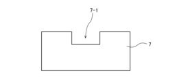
- FIG. 2 is a plan view showing an example of a metal foil element.
- FIG. 3 is a cross-sectional view that illustrates the cutting process.
- FIG. 4 is a plan view that illustrates the cutting process.
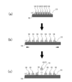
- FIG. 5 is a schematic cross-sectional view showing the expanding step and the picking up step.
- 6A to 6C are schematic cross-sectional views showing a method for manufacturing a power semiconductor device.
- FIG. 7 is a plan view showing a layout of lines to cut according to the first modified example.
- FIG. 8 is a plan view showing a layout of lines to cut according to the second modification.
- FIG. 1 is a cross-sectional view showing a power semiconductor device 1 using a metal foil element 7 according to this embodiment.
- This power semiconductor device 1 generally includes a substrate 2, a power semiconductor element 5, and a metal foil element 7.
- the substrate 2 is an insulating substrate, such as a ceramic substrate.
- a metal layer 3 is formed on the substrate 2 as wiring. Furthermore, a pad 4 and a power semiconductor element 5 are disposed on the metal layer 3.
- the power semiconductor element 5 is a semiconductor chip.
- the metal foil element 7 is adhered to the power semiconductor element 5 via a conductive adhesive layer 6.
- the metal foil element 7 is connected to the pad 4 via a wire 8.
- the metal foil element 7 can promote heat dissipation from the power semiconductor element 5.
- the power semiconductor element 5 can be electrically connected to the pad 4 via the metal foil element 7.
- Another advantage of this configuration is the reliability of wire bonding. That is, the difference in linear expansion coefficient between the metal foil element 7 and the wire 8 is usually smaller than the difference in linear expansion coefficient between the power semiconductor element 5 and the wire 8. Therefore, by using the metal foil element 7, the reliability of wire bonding can be improved compared to the case where the wire 8 is directly bonded to the power semiconductor element 5.
- FIG. 2 is a plan view showing an example of a metal foil element 7.
- the metal foil element 7 has a special shape. Specifically, the metal foil element 7 has a shape other than a rectangle. More specifically, the metal foil element 7 has a rectangular shape with a notch 7-1 formed on one side.
- a manufacturing method for manufacturing the metal foil element 7 has been devised.
- the manufacturing method for the metal foil element 7 is described below.
- the manufacturing method for the metal foil element 7 includes a cutting process (step S1), an expanding process (step S2), and a picking up process (step S3). Each process will be described in detail below.
- Step S1 Cutting Step Fig. 3 is a cross-sectional view that illustrates the cutting step, and Fig. 4 is a plan view that illustrates the cutting step.
- a ring frame 12 with a dicing tape 9 attached is prepared.
- a metal foil 14 is placed on the dicing tape 9.
- the metal foil 14 is provided as a laminate 11 with a bonding film-like material 13. That is, the laminate 11 is placed on the dicing tape 9.
- the laminate 11 is placed on the dicing tape 9 so that the metal foil 14 faces upward.
- the bonding film-like material 13 is the part that is ultimately fired to become the adhesive layer 6 (see FIG. 1).
- the bonding film-like material 13 has a structure in which, for example, a thermally conductive material having electrical conductivity is dispersed in a binder.
- a planned cutting line 17 is set on the metal foil 14. Then, the laminate 11 is cut along the planned cutting line 17.
- the metal foil 14 and the bonding film-like material 13 in the laminate 11 not only can the metal foil 14 and the bonding film-like material 13 be cut simultaneously, but it is also possible to cut the metal foil 14 and the bonding film-like material 13 into exactly the same shape.
- the planned cutting line 17 has a complex shape.
- the planned cutting line 17 has an element formation line 17-1 and an excess area division line 17-2.
- the element formation line 17-1 is a line for separating the element formation region 15 from its surrounding areas.
- the element formation line 17-1 corresponds to the outer periphery of the element formation region 15.
- the element formation region 15 is the portion that will become the metal foil element 7.
- multiple element formation regions 15 are set on the metal foil 14.
- the multiple element formation regions 15 are spaced apart from each other. However, there may be only one element formation region 15.
- the excess area separation lines 17-2 are provided to enable the next process, the expanding process (step S2), to be carried out.
- the excess area separation lines 17-2 separate the excess area 16 into multiple regions.
- the excess area 16 is the area of the metal foil 14 other than the element formation region 15.
- the excess area dividing lines 17-2 are set so that each element formation region 15 is connected to the outer periphery of the metal foil 14 via the intended cutting lines 17 at least in two places. That is, each element formation region 15 is connected to the outer periphery of the metal foil 14 at least in two places via the excess area dividing lines 17-2, or via the excess area dividing lines 17-2 and the element formation lines 17-1 that divide the other element formation regions 15.
- the excess area dividing lines 17-2 are set on a plurality of straight lines extending in a lattice pattern.
- Each element formation region 15 is connected to both the excess area dividing lines 17-2 that extend vertically and the excess area dividing lines 17-2 that extend horizontally. With this configuration, each element formation region 15 is connected to the outer periphery of the metal foil 14 at least in two places. As a result, the excess area 16 is divided into a plurality of regions.
- the cut laminate 11 is supported on a stretchable sheet, and the stretchable sheet is stretched. This widens the gap between the element formation region 15 and the surrounding region.
- simply cutting the laminate 11 along the element formation line 17-1 would result in the element formation region 15 being surrounded by a closed surplus region 16.
- a closed surplus region 16 exists outside the element formation region 15, the gap between the element formation region 15 and the surrounding region cannot be widened even if the expanding process is performed. In other words, the expanding process cannot be performed in practice.
- the presence of the surplus region separation line 17-2 prevents the formation of a closed region surrounding each element formation region 15. Therefore, in the expanding process, it is possible to widen the gap between each element formation region 15 and the surrounding region.
- the intended cutting line 17 since the intended cutting line 17 has a complex shape, it is difficult to adopt a means (such as a rotating blade) that can cut only in a straight line. Therefore, a method that can cut at any position is adopted as the cutting means. Examples of such methods include laser ablation, chemical etching, and plasma etching. In addition, if the cutting means is laser ablation, chemical etching, plasma etching, etc., it becomes easy to adjust the value of X/Y in the modified example 2 described below.
- these cutting means since the chemical properties of the metal foil 14 and the bonding film-like material 13 are different, a method that does not rely on chemical action is desirable. From this viewpoint, it is preferable to adopt laser ablation or plasma etching. In addition, it is more preferable to use laser ablation, since it is easier to melt and cut the inorganic and metal materials contained in the bonding film material 13.
- Step S2 Expanding Step Next, the expanding step is carried out.
- Figures 5(a) and 5(b) are schematic cross-sectional views showing the expanding step. As described above, in the expanding step, the extensible sheet 18 is expanded while the laminate 11 is supported on the extensible sheet 18.
- the cut laminate 11 is transferred from the dicing tape 9 onto the extensible sheet 18, and the laminate 11 is adhered to the extensible sheet 18 (Fig. 5(a)).
- the extensible sheet 18 is then stretched in the planar direction (Fig. 5(b)). This causes the spacing between the cut portions to increase. In other words, the spacing between each element formation region 15 and the surrounding regions increases.
- FIG. 5(c) is a schematic cross-sectional view showing the pick-up process.
- each element formation region 15 metal foil element 7
- the metal foil element 7 is unlikely to interfere with its surrounding parts.
- the bonding film-like materials 13 are unlikely to come into contact with each other. Therefore, it is possible to appropriately pick up the metal foil element 7.
- the method described above allows the metal foil element 7 according to this embodiment to be obtained.
- the obtained metal foil element 7 is used to manufacture the power semiconductor device 1 according to the process (step S4) described below.
- FIG. 6 is a schematic cross-sectional view showing a manufacturing method of the power semiconductor device 1. As shown in FIG.
- a substrate 2 on which a power semiconductor element 5 is mounted is prepared.
- the picked-up metal foil element 7 is bonded to the upper surface of the power semiconductor element 5.
- the metal foil element 7 is temporarily fixed on the power semiconductor element 5 via the bonding film-like material 13.
- the bonding film-like material 13 is fired. This decomposes organic substances such as binders in the bonding film-like material 13.
- the conductive thermally conductive material is metal particles as described below, the metal particles may be fused to form an adhesive layer 6 made of a thermally conductive material. That is, as shown in FIG. 6(b), the metal foil element 7 is bonded to the power semiconductor element 5 via the adhesive layer 6.
- the firing of the bonding film-like material 13 and the firing of the firing material between the power semiconductor element 5 and the substrate 2 may be performed at the same time.
- the metal foil element 7 is connected to the pad 4 via the wire 8. This completes the power semiconductor device 1 according to this embodiment.
- step S1 a specific shape of surplus area dividing line 17-2 is set on the planned cutting line 17 set in the cutting process. This makes it possible to carry out the expanding process (step S2). This makes it possible to avoid interference between the metal foil element 7 and the surrounding area in the picking up process (step S3), making it possible to easily pick up the metal foil element 7.
- the metal foil element 7 has a rectangular shape with a notch 7-1 formed on one side.
- the shape of the metal foil element 7 is not limited to this shape.
- hollowing out is generally considered.
- simply hollowing out the metal foil element 7 does not effectively allow the expansion process to be carried out. Therefore, according to this embodiment, it is effective to set the excess area separation line 17-2 so that expansion can be carried out.
- the above-mentioned "special shape” for which hollowing is generally considered is a shape other than a rectangle.
- Examples of the "shape other than a rectangle” include the following shapes. (1) A shape that cannot be formed by simply setting multiple straight lines extending from one periphery to the other periphery of the metal foil 14. (2) A shape that cannot be processed by a means capable of cutting only in straight lines, such as a rotating blade. (3) A shape that has a curved portion. (4) A shape that has a convex or concave portion (notch) on one side.
- vertexs also include those with angles of more than 180°.
- the metal foil element 7 is simply rectangular (a rectangular shape without cutouts, etc.), if multiple element formation regions 15 are set apart from one another in the metal foil 14, it is common to adopt a hollowing out process as a manufacturing method. However, as mentioned above, the expansion process cannot be carried out if hollowing out is simply performed. Therefore, even if the metal foil element 7 is rectangular, in cases where multiple element formation regions 15 are set apart, it is effective to set the excess region separation line 17-2 according to this embodiment so that expansion can be carried out.
- the dicing tape 9 itself may be used as the extensible sheet 18.
- the extensible sheet 18 may be laminated on the laminate 11 in advance at the cutting step (step S1). That is, the laminate 11 may be placed on the dicing tape 9 via the extensible sheet 18.
- the dicing tape 9 is peeled off from the extensible sheet 18 before the expanding step (step S2). In the above cases, it is not necessary to transfer the laminate 11.
- the extensible sheet 18 may be laminated with the bonding film material 13 via an adhesive layer, or may be laminated directly with the bonding film material 13 without an adhesive layer.
- the adhesive layer can be formed from an energy ray curable adhesive, or from an adhesive that does not cure with energy rays.
- the metal foil 14 is placed on the dicing tape 9 as a laminate 11 with the bonding film-like material 13.
- a bonding composite sheet may be prepared in which the bonding film-like material 13 is a sheet laminated on the dicing tape 9 in advance, and the metal foil 14 may be placed on the bonding film-like material 13 of the bonding composite sheet.
- the bonding composite sheet is convenient because the dicing tape 9 and the bonding film-like material 13 are provided as a set.
- these resins can be used as ionomers by adding a metal ion crosslinking agent. Furthermore, these resins may be subjected to a modification treatment in which they are crosslinked by electron beam irradiation, etc. In addition, when the substrate has self-adhesive properties, the substrate may also serve as the adhesive layer.
- the metal foil element 7 is described as being used in a power semiconductor device 1 that utilizes a die-top system.
- the uses of the metal foil element 7 are not limited to such uses.
- the metal foil element 7 can also be suitably used as a heat dissipation material for other electronic components, such as semiconductor devices and batteries that are used for purposes other than power control or conversion.
- a bonding film-like material 13 which is included in the laminate 11 together with the metal foil 14, is configured to have a conductive thermally conductive material dispersed in a binder.
- a bonding film-like material 13 is suitable for use in a power semiconductor device such as a die-top system using a metal foil element 7.
- a suitable example of such a bonding film-like material 13 is a film-like sintered material containing metal particles as described in WO2019/163568.
- This film-like sintered material is a film-like sintered material containing first metal particles, second metal particles, and a binder component.
- the first metal particles have an average particle diameter of 100 nm or less, and a maximum particle diameter of 250 nm or less.
- the second metal particles have an average particle diameter of 1000 to 7000 nm, a minimum particle diameter of more than 250 nm, and a maximum particle diameter of 10000 nm or less.
- the mass ratio represented by the first metal particles/second metal particles is 0.1 or more.
- the metal species of the metal particles include silver, gold, copper, iron, nickel, aluminum, silicon, palladium, platinum, titanium, barium titanate, oxides or alloys thereof, and the like, with silver and silver oxide being preferred.
- binder components that can be included in the film-shaped fired material together with the metal particles include resins.
- resins include acrylic resins, polycarbonate resins, polylactic acid, and polymers of cellulose derivatives, with acrylic resins being preferred.
- the thermally conductive material contained in the bonding film-like material 13 does not necessarily have to be electrically conductive. Even if an insulating thermally conductive material is used, depending on the application, the metal foil element 7 can be suitably used for heat dissipation.
- other materials constituting the bonding film-like material 13 include film-like sintered materials containing inorganic thermally conductive materials, such as the green sheets for obtaining boron nitride sintered bodies described in WO2022/163646.
- the bonding film-like material 13 is baked to form the adhesive layer 6. That is, the bonding film-like material 13 is a film-like baked material, preferably a film-like baked material containing metal particles or an inorganic thermally conductive material.
- the bonding film-like material 13 does not necessarily have to be a baked material.
- a curable adhesive sheet such as an adhesive sheet made of an epoxy resin composition containing a thermally conductive material such as alumina or boron nitride, as described in JP 2014-156531 A, can also be used as the bonding film-like material 13.
- the curable adhesive sheet may contain a thermally conductive and electrically conductive material such as the above-mentioned metal particles.
- the metal foil 14 does not necessarily have to be processed in the state of the laminate 11. That is, the metal foil 14 may be processed separately.
- the metal foil element 7 can be attached to the power semiconductor element 5 even if the metal foil element 7 is processed separately.
- FIG. 7 is a plan view showing the layout of the intended cutting lines 17 in Modification 1.
- the element formation region 15 is rectangular with a notch on one side.
- the excess region separation line 17-2 is connected to the element formation region 15 at a position different from the portion where the notch is provided.
- each excess area 16 after cutting will have a complex shape.
- each excess area 16 after cutting will not have a complex shape, so that contact between adjacent areas can be prevented in the expansion process (step S2).
- FIG. 8 is a plan view showing the layout of the intended cutting lines 17 according to the second modified example.
- the excess area dividing lines 17-2 have first lines 17-2-1 located on X straight lines extending along a first direction, and second lines 17-2-2 located on Y straight lines extending along a second direction perpendicular to the first direction.
- 0.65 ⁇ X/Y ⁇ 1.5 0.65 ⁇ X/Y ⁇ 1.5.
- FIG. 8 shows an example in which both X and Y are 5.
- the intervals of the cut portions are easily expanded uniformly in the expanding process (step S2). For example, if the area between adjacent areas in a part of the cut portion is excessively expanded, a large stress is generated in the extensible sheet 18 in that area, and the extensible sheet 18 is easily torn. On the other hand, if the expansion is insufficient, the metal foil element 7 is easily brought into contact with its surrounding area in the pick-up process (step S3). In particular, if the element formation area 15 has a special shape, the shapes of the multiple areas formed after cutting are likely to be non-uniform. Therefore, it is difficult to uniformly expand the area between adjacent areas in the expanding process.
- an extra excess area dividing line 17-2 (an excess area dividing line 17-2 that is not connected to the element forming region 15) is intentionally provided to bring the ratio of X/Y closer to 1 and achieve the above-mentioned effect.
- the excess area dividing line 17-2 (first line 17-2-1) is connected to the notch in the element formation region 15.
- the excess area dividing line 17-2 may be connected to the element formation region 15 at a position different from the portion where the notch is provided.
- the individual shapes formed after cutting are not complicated.
- the shapes tend to be non-uniform between multiple regions, and it tends to be difficult to uniformly expand between adjacent regions in the expansion process.
- 0.65 ⁇ X/Y ⁇ 1.5 so it is easier to uniformly expand between adjacent regions.
- the method for manufacturing the metal foil element 7 includes a cutting step of setting a cutting line 17 on the metal foil 14 and cutting the metal foil 14 along the cutting line 17.
- the cutting line 17 includes an element formation line 17-1 corresponding to the outer periphery of the element formation region 15 and an excess region dividing line 17-2 dividing the excess region 16, which is a region other than the element formation region 15, into a plurality of regions.
- the element formation region has a shape other than a rectangle.
- the element formation region is connected to the outer periphery of the metal foil at least in two places via the cutting line.
- the excess region 16 is divided into a plurality of regions by the excess region dividing line 17-2 so that the expansion step can be performed, so that the expansion can be performed after the cutting step even if the element formation region has a special shape. This makes it difficult for the metal foil element 7 to come into contact with its surrounding regions during pick-up, making it possible to properly pick up the element.
- the manufacturing method of the metal foil element 7 includes a cutting step of setting a cutting line 17 on the metal foil 14 and cutting the metal foil 14 along the cutting line 17.
- the cutting line 17 includes an element formation line 17-1 corresponding to the outer periphery of the element formation region 15 and an excess region dividing line 17-2 dividing the excess region 16, which is a region other than the element formation region 15, into a plurality of regions.
- a plurality of element formation regions 15 are set at a distance from each other.
- Each of the plurality of element formation regions 15 is connected to the outer periphery of the metal foil 14 at least at two places via the cutting line 17.
- the excess region 16 is divided into a plurality of regions by the excess region dividing line 17-2 so that the expansion step can be performed, so that the expansion can be performed after the cutting step even though the plurality of element formation regions are set at a distance from each other.
- the metal foil element 7 is less likely to come into contact with its surrounding regions during pick-up, making it possible to properly pick up the element.
- an expanding step is performed in which the extensible sheet 18 is expanded while the metal foil is supported on the extensible sheet 18.
- the expanding step separates the element formation region 15 from the surrounding area. This allows the element formation region 15 to be easily picked up.
- the metal foil 14 is cut by laser ablation, chemical etching, or plasma etching. By using such methods, it is possible to cut the metal foil at any desired position.
- the element formation region 15 is rectangular with a notch on at least one side.
- the excess region separation line 17-2 is connected to the element formation line 17-1 at a position different from the portion where the notch is provided.
- the excess area dividing line 17-2 has a first line 17-2-1 located on X straight lines extending along a first direction, and a second line 17-2-2 located on Y straight lines extending along a second direction perpendicular to the first direction.
- 0.65 ⁇ X/Y ⁇ 1.5 0.65 ⁇ X/Y ⁇ 1.5.
- the metal foil 14 is prepared as a laminate 11 with a bonding film-like material 13 containing a thermally conductive material. Then, in the cutting process, the laminate 11 is cut to cut the metal foil 14. With this configuration, a metal foil element 7 laminated with a bonding film-like material 13 can be obtained. Furthermore, by simultaneously cutting the metal foil 14 and the bonding film-like material 13, not only can the metal foil 14 and the bonding film-like material 13 be cut simultaneously, but the metal foil 14 and the bonding film-like material 13 can also be cut into exactly the same shape. Then, the metal foil element 7 can be used as a heat dissipation material simply by placing the metal foil element 7 on a component that is to be dissipated heat.
- a metal foil element 7 is bonded to the power semiconductor element. This makes it possible to obtain a power semiconductor device having a heat dissipation material.
Landscapes
- Dicing (AREA)
- Cooling Or The Like Of Semiconductors Or Solid State Devices (AREA)
Abstract
金属箔素子の製造方法は、金属箔を切断予定ラインに沿って切断する切断工程と、切断工程の後に、素子形成領域を金属箔素子7としてピックアップするピックアップ工程とを備える。切断予定ラインは、素子形成ラインと、エキスパンド工程が実施可能となるように余剰領域を複数の領域に分断する、余剰領域分断ラインとを含む。素子形成領域は、少なくとも2か所で、余剰領域分断ラインを介して金属箔の外周に接続されている。
Description
本発明は、金属箔素子及びパワー半導体装置の製造方法に関する。
金属箔素子は、様々な場面で使用されている。例えば、非特許文献1(Heraeus Electronics, Die Top System(DTS)-Get the most out of your power module、インターネット(URL:https://www.heraeus.com/en/het/products_and_solutions_het/material_systems/die_top_system/dts_page.html))には、パワーモジュールに関する技術として、ダイトップシステムと称される技術が記載されている。非特許文献1には、ダイ(チップ)上に、焼結ペーストを介して特殊な形状を有する銅箔を貼り付ける点が記載されている。具体的には、銅箔として、概ね矩形状であるが、1つの辺に切り欠きを有する形状を有するものが記載されている。
特殊な形状(例えば矩形以外の形状)を有する金属箔素子を作製する手段として、パンチング等の中抜き加工が考えられる。この場合、まず、金属箔が準備される。そして、金属箔素子の形状に沿って、金属箔が切り抜かれる。具体的には、金属箔素子の形状に沿って金属箔が切断され、切断後に金属箔素子がピックアップされる。
しかしながら、中抜き加工を用いた場合は、ピックアップ時に、金属箔素子が金属箔の余剰部分と接触してしまい、適切にピックアップすることが出来ない場合がある。
また、金属箔素子が特殊な形状ではなかったとしても、1枚の金属箔から複数の金属箔素子を作製する際に、金属箔素子となる領域を互いに離間させて設定した場合には、通常、中抜き加工が検討される。そのため、特殊な形状の場合と同様の問題が生じ得る。
そこで、本発明の目的は、金属箔素子を適切にピックアップすることのできる技術を提供することにある。
一態様において、本発明に係る金属箔素子の製造方法は、金属箔に切断予定ラインを設定し、切断予定ラインに沿って金属箔を切断する切断工程を備える。切断予定ラインは、素子形成領域の外周に対応する素子形成ラインと、素子形成領域以外の領域である余剰領域を複数の領域に分断する、余剰領域分断ラインとを含む。素子形成領域は、矩形以外の形状である。素子形成領域は、少なくとも2か所で、切断予定ラインを介して金属箔の外周に接続されている。
他の一態様において、本発明に係る金属箔素子の製造方法は、金属箔に切断予定ラインを設定し、切断予定ラインに沿って金属箔を切断する切断工程を備える。切断予定ラインは、素子形成領域の外周に対応する素子形成ラインと、素子形成領域以外の領域である余剰領域を複数の領域に分断する、余剰領域分断ラインとを含む。素子形成領域は、互いに離間して複数設定されている。複数の素子形成領域の各々は、少なくとも2か所で、切断予定ラインを介して金属箔の外周に接続されている。
本発明によれば、金属箔素子を適切にピックアップすることのできる技術が提供される。
以下に、図面を参照しつつ、本発明の実施形態に係る金属箔素子の製造方法について説明する。なお、以下の実施形態においては、一例として、金属箔素子が、ダイトップシステムを利用したパワー半導体装置に使用される場合について説明する。ただし、本実施形態により製造される金属箔素子の用途は、このような用途に限定されるものではない。
まず、金属箔素子を用いて製造されるパワー半導体装置の構成について説明する。図1は、本実施形態に係る金属箔素子7を用いたパワー半導体装置1を概略的に示す断面図である。このパワー半導体装置1は、概略的には、基板2、パワー半導体素子5、及び金属箔素子7を有している。
基板2は、例えばセラミック等の絶縁性の基板である。基板2上には、配線として金属層3が形成されている。また、金属層3上には、パッド4及びパワー半導体素子5が配置されている。パワー半導体素子5は、半導体チップである。
金属箔素子7は、導電性の接着層6を介してパワー半導体素子5上に接着されている。また、金属箔素子7は、ワイヤ8を介してパッド4に接続されている。このような構成によれば、金属箔素子7により、パワー半導体素子5の放熱を促進させることができる。また、金属箔素子7を介してパワー半導体素子5をパッド4と電気的に接続することが出来る。また、このような構成の他の利点は、ワイヤーボンディングの信頼性である。すなわち、金属箔素子7とワイヤ8との間の線膨張係数の差は、通常、パワー半導体素子5とワイヤ8との間の線膨張係数の差よりも小さい。従って、金属箔素子7を用いることにより、パワー半導体素子5にワイヤ8を直接ボンディングする場合に比べて、ワイヤーボンディングの信頼性を向上させることが出来る。
図2は、金属箔素子7の一例を示す平面図である。図2に示されるように、金属箔素子7は、特殊な形状を有している。具体的には、金属箔素子7は、矩形以外の形状である。詳細には、矩形における1つの辺に切り欠き7-1を形成した形状を有している。
ここで、本実施形態では、金属箔素子7を製造するための製造方法が工夫されている。以下に、金属箔素子7の製造方法について説明する。
本実施形態に係る金属箔素子7の製造方法は、切断工程(ステップS1)と、エキスパンド工程(ステップS2)と、ピックアップ工程(ステップS3)とを有している。以下、各工程について詳述する。
(ステップS1)切断工程
図3は、切断工程を概略的に示す工程断面図である。また、図4は、切断工程を概略的に示す平面図である。
図3は、切断工程を概略的に示す工程断面図である。また、図4は、切断工程を概略的に示す平面図である。
まず、図3(a)及び図4(a)に示されるように、ダイシングテープ9が貼り付けられたリングフレーム12を準備する。そして、金属箔14をダイシングテープ9上に設置する。本実施形態においては、金属箔14は、接合用フィルム状材料13との積層体11として提供される。すなわち、積層体11が、ダイシングテープ9上に配置される。積層体11は、金属箔14が上側を向くように、ダイシングテープ9上に配置される。
なお、接合用フィルム状材料13は、最終的に焼成され、接着層6(図1参照)となる部分である。接合用フィルム状材料13は、例えば、導電性を有する熱伝導性材料がバインダー中に分散した構成を有している。
続いて、図3(b)及び図4(b)に示されるように、金属箔14に、切断予定ライン17が設定される。そして、切断予定ライン17に沿って積層体11が切断される。積層体11において、金属箔14と接合用フィルム状材料13が同時に切断されることで、金属箔14と接合用フィルム状材料13の切断を同時に行えるだけでなく、金属箔14と接合用フィルム状材料13を正確に同一の形状に切断することが可能である。
ここで、図4(b)に示されるように、切断予定ライン17は、複雑な形状を有している。詳細には、切断予定ライン17は、素子形成ライン17-1と、余剰領域分断ライン17-2とを有している。
素子形成ライン17-1は、素子形成領域15をその周囲の部分から切り離すためのラインである。すなわち、素子形成ライン17-1は、素子形成領域15の外周に対応している。素子形成領域15は、金属箔素子7となる部分である。本実施形態において、素子形成領域15は、金属箔14上に複数設定されている。複数の素子形成領域15は、互いに離間している。ただし、素子形成領域15は、単一であってもよい。
一方、余剰領域分断ライン17-2は、次の工程であるエキスパンド工程(ステップS2)を実施可能とするために設けられている。余剰領域分断ライン17-2は、余剰領域16を複数の領域に分断している。余剰領域16とは、金属箔14における素子形成領域15以外の領域である。
余剰領域分断ライン17-2は、各素子形成領域15が少なくとも2か所で切断予定ライン17を介して金属箔14の外周に接続されるように設定されている。すなわち、各素子形成領域15は、少なくとも2か所において、余剰領域分断ライン17-2を介して、あるいは、余剰領域分断ライン17-2及び他の素子形成領域15を区画する素子形成ライン17-1を介して、金属箔14の外周に接続されている。図4(b)に示される具体例においては、余剰領域分断ライン17-2は、格子状に伸びる複数の直線上に設定されている。個々の素子形成領域15は、縦に伸びる余剰領域分断ライン17-2と、横に伸びる余剰領域分断ライン17-2との両方に接続されている。このような構成により、各素子形成領域15が、少なくとも2か所において、金属箔14の外周に接続されている。その結果、余剰領域16が、複数の領域に分断されている。
後述のエキスパンド工程では、切断後の積層体11が伸張性シート上に支持され、伸張性シートが伸張される。これにより、素子形成領域15とその周囲の領域との間隔が広げられる。ここで、単に素子形成ライン17-1に沿って積層体11を切断するだけでは、素子形成領域15が、閉じた形状の余剰領域16により囲まれることになる。素子形成領域15の外側に閉じた余剰領域16が存在していると、エキスパンド工程を実施しても、素子形成領域15とその周囲の領域との間隔を広げることはできない。すなわち、実質的にエキスパンド工程を実施できない。これに対して、本実施形態では、余剰領域分断ライン17-2の存在により、各素子形成領域15を取り囲む閉じた領域が形成されなくなっている。そのため、エキスパンド工程において、各素子形成領域15とその周囲の領域との間隔を広げることが可能となっている。
上述のように、本実施形態においては、切断予定ライン17が、複雑な形状を有しているため、直進方向にのみ切断することのできる手段(例えば回転ブレード等)を採用することが難しい。そのため、切断手段として、任意の位置において切断を行うことが出来る手法が採用される。そのような手法として、例えばレーザーアブレーション、ケミカルエッチング、及びプラズマエッチング等を挙げることが出来る。また、切断手段が、レーザーアブレーション、ケミカルエッチング、又はプラズマエッチング等であれば、後述する変形例2において、X/Yの値を調整することが容易となる。すなわち、第1方向に沿って延びるX本の直線上に位置する第1ライン17-2-1と、第1方向に垂直な第2方向に沿って延びるY本の直線上に位置する第2ライン17-2-2とを、を所望の位置に、所望の本数で形成することが容易になる。これらの切断手段のうちでも、金属箔14と接合用フィルム状材料13の化学的な性質が異なるため、化学的な作用によらない手法が望ましい。この観点から、レーザーアブレーション又はプラズマエッチングを採用することが好ましい。また、接合用フィルム状材料13に含まれる無機材料や、金属材料も溶融させて切断しやすい観点から、レーザーアブレーションを採用することがより好ましい。
(ステップS2)エキスパンド工程
続いて、エキスパンド工程を実施する。図5(a)及び(b)は、エキスパンド工程を示す概略断面図である。既述のように、エキスパンド工程では、伸張性シート18上に積層体11を支持させた状態で、伸張性シートを伸長させる。
続いて、エキスパンド工程を実施する。図5(a)及び(b)は、エキスパンド工程を示す概略断面図である。既述のように、エキスパンド工程では、伸張性シート18上に積層体11を支持させた状態で、伸張性シートを伸長させる。
具体的には、まず、切断後の積層体11を、ダイシングテープ9から伸張性シート18上に移し替え、積層体11を伸張性シート18に接着させる(図5(a))。そして、伸張性シート18を面方向に伸長する(図5(b))。これにより、切断された部分の間隔が広がる。すなわち、各素子形成領域15とその周囲の領域との間隔が広がる。
(ステップS3)ピックアップ工程
続いて、素子形成領域15を、金属箔素子7としてピックアップする。図5(c)は、ピックアップ工程を示す概略断面図である。図5(c)に示されるように、各素子形成領域15(金属箔素子7)を、接合用フィルム状材料13とともに、伸張性シート18から引き離す。この際、ステップS2において金属箔素子7とその周囲の部分との間隔が広げられているから、金属箔素子7がその周囲の部分と干渉し難い。また、接合用フィルム状材料13同士も接触し難い。従って、適切に金属箔素子7をピックアップすることが可能となる。
続いて、素子形成領域15を、金属箔素子7としてピックアップする。図5(c)は、ピックアップ工程を示す概略断面図である。図5(c)に示されるように、各素子形成領域15(金属箔素子7)を、接合用フィルム状材料13とともに、伸張性シート18から引き離す。この際、ステップS2において金属箔素子7とその周囲の部分との間隔が広げられているから、金属箔素子7がその周囲の部分と干渉し難い。また、接合用フィルム状材料13同士も接触し難い。従って、適切に金属箔素子7をピックアップすることが可能となる。
以上説明した方法によって、本実施形態に係る金属箔素子7が得られる。なお、得られた金属箔素子7は、以下に説明する工程(ステップS4)に従って、パワー半導体装置1の製造のために使用される。
(ステップS4)パワー半導体装置の製造
図6は、パワー半導体装置1の製造方法を示す概略断面図である。
図6は、パワー半導体装置1の製造方法を示す概略断面図である。
まず、図6(a)に示されるように、パワー半導体素子5が搭載された基板2を用意する。そして、ピックアップされた金属箔素子7を、パワー半導体素子5の上面に接着する。金属箔素子7は、接合用フィルム状材料13を介して、パワー半導体素子5上に仮固定される。次いで、接合用フィルム状材料13を焼成する。これにより、接合用フィルム状材料13中のバインダー等の有機物が分解される。また、導電性を有する熱伝導性材料が、後述するように金属粒子である場合には、場合により金属粒子が融着し、熱伝導性材料からなる接着層6が形成される。すなわち、図6(b)に示されるように、金属箔素子7が接着層6を介してパワー半導体素子5に接合される。なお、パワー半導体素子5を基板2(金属層3)上に別の焼成材料により仮固定していた場合には、接合用フィルム状材料13の焼成と、パワー半導体素子5と基板2との間の焼成材料の焼成とを一括して行ってもよい。
次いで、図6(c)に示されるように、ワイヤ8を介して金属箔素子7をパッド4に接続する。これにより、本実施形態に係るパワー半導体装置1が得られる。
以上、パワー半導体装置1を製造する場合を例に挙げて、本実施形態に係る金属箔素子7の製造方法について説明した。本実施形態によれば、切断工程(ステップS1)において設定される切断予定ライン17に、特定形状の余剰領域分断ライン17-2が設定されている。そのため、エキスパンド工程(ステップS2)を実施することが可能となる。これにより、ピックアップ工程(ステップS3)において、金属箔素子7とその周囲の領域との干渉を避けることができ、容易に金属箔素子7をピックアップすることが可能となる。
なお、本実施形態においては、金属箔素子7が、矩形における1つの辺に切り欠き7-1を形成した形状を有している場合について説明した。しかし、金属箔素子7の形状は、このような形状に限定されるものではない。金属箔素子7の形状が、特殊な形状をしている場合には、一般的には中抜き加工が検討される。しかし、単に金属箔素子7を中抜きしただけでは、既述の通り、エキスパンド工程が実質的に実施できない。そこで、本実施形態に従って、エキスパンドが実施可能となるように余剰領域分断ライン17-2を設定することが有効である。
なお、一般的に中抜き加工が検討される上述の「特殊な形状」としては、矩形以外の形状が考えられる。「矩形以外の形状」としては、例えば、以下の形状が考えられる。
(1)金属箔14の外周から外周にまで延びる複数の直線を設定しただけでは形成することのできない形状
(2)回転ブレード等の直線状にのみ切断が可能な手段によっては加工することのできない形状
(3)曲線部を有する形状
(4)1つの辺に凸部または凹部(切り欠き)を有する形状
(1)金属箔14の外周から外周にまで延びる複数の直線を設定しただけでは形成することのできない形状
(2)回転ブレード等の直線状にのみ切断が可能な手段によっては加工することのできない形状
(3)曲線部を有する形状
(4)1つの辺に凸部または凹部(切り欠き)を有する形状
ここで、上記の(1)について詳述すると、このような形状は、直線部のみから構成される多角形状であっても、金属箔14の一端から他端まで接続する2本以上の直線の交差によって形成することができない頂点が存在し、又は、金属箔14の一端から他端まで接続する直線によって形成することができない辺が存在する。なお、「頂点」には角度が180°超であるものも含まれる。
一方で、金属箔素子7が単なる矩形状(切り欠きなどのない矩形状)である場合であっても、金属箔14に複数の素子形成領域15が互いに離間して設定される場合には、製造方法として中抜き加工を採用することが一般的である。しかしながら、既述の通り、単に中抜きを行った場合にはエキスパンド工程が実施できない。そのため、金属箔素子7が矩形状であっても、複数の素子形成領域15が離間して設定される場合等においては、本実施形態に従って、エキスパンドが実施可能となるように余剰領域分断ライン17-2を設定することが有効である。
なお、本実施形態においては、エキスパンド工程(ステップS2)において、積層体11がダイシングテープ9から伸張性シート18(図5参照)に移し替えられる場合について説明した。しかしながら、ダイシングテープ9自体が伸張性シート18として使用されてもよい。あるいは、切断工程(ステップS1)の段階で、予め、伸張性シート18が積層体11に積層されていてもよい。すなわち、ダイシングテープ9上に、伸張性シート18を介して積層体11が配置されていてもよい。この場合には、切断工程(ステップS1)の完了の後、エキスパンド工程(ステップS2)までの間に、ダイシングテープ9を伸張性シート18から剥離する。以上の場合には、積層体11を移し替える必要はない。また、伸張性シート18は、粘着剤層を介して接合用フィルム状材料13と積層されていてもよいし、粘着剤層を介することなく直接接合用フィルム状材料13と積層されていてもよい。粘着剤層を用いる場合、粘着剤層としては、エネルギー線硬化性の粘着剤により形成することもできるし、エネルギー線によっては硬化しない性質の粘着剤を用いて形成することもできる。また、本実施形態では、金属箔14が、接合用フィルム状材料13との積層体11としてダイシングテープ9上に設置される場合について説明した。しかしながら、接合用フィルム状材料13が、あらかじめダイシングテープ9上に積層された形態のシートである、接合用複合シートを用意し、接合用複合シートの接合用フィルム状材料13上に、金属箔14を設置してもよい。接合用複合シートは、ダイシングテープ9と接合用フィルム状材料13がセットの状態で提供されるため、便利である。
伸張性シート18の粘着剤層は、一般的にはシート形状を維持する強度がないため、伸張性シート18は、通常、基材を備える。基材の材質としては樹脂フィルムが好ましく、樹脂フィルムを形成するための樹脂としては、エキスパンドに適した柔軟性を付与するする観点から、ポリエチレン、ポリプロピレン等のポリオレフィン樹脂、エチレン-メタクリル酸共重合体、エチレン-酢酸ビニル共重合体等のオレフィン共重合体、ポリブチレンテレフタレート、ウレタンアクリレート又はウレタンメタクリレートの硬化膜、塩化ビニル、柔軟性ポリエステル樹脂等であることが好ましい。また、これらの樹脂に金属イオン架橋剤を添加し、アイオノマーとして用いることもできる。さらに、これらの樹脂を電子線照射等により架橋する改質処理を施してもよい。また、基材が自着性を有する場合には、基材は粘着剤層をも兼ねることができる場合がある。
本実施形態では、金属箔素子7が、ダイトップシステムを利用したパワー半導体装置1に使用される場合について説明した。ただし、金属箔素子7の用途は、このような用途に限定されない。例えば、金属箔素子7は、電力の制御又は変換以外の用途に用いられる半導体装置、バッテリー等の、他の電子部品の放熱材料等としても好適に用いることが出来る。
本実施形態では、金属箔14とともに積層体11に含まれる接合用フィルム状材料13として、導電性を有する熱伝導性材料がバインダー中に分散した構成のものが使用される場合について説明した。このような接合用フィルム状材料13は、ダイトップシステム等のパワー半導体装置用に金属箔素子7を使用する場合に好適である。このような接合用フィルム状材料13の好適な例として、WO2019/163568に記載されているような金属粒子を含むフィルム状焼成材料が挙げられる。このフィルム状焼成材料は、第1の金属粒子、第2の金属粒子及びバインダー成分を含有するフィルム状焼成材料である。第1の金属粒子の平均粒子径は100nm以下であり、かつ最大粒子径が250nm以下である。第2の金属粒子の平均粒子径は1000~7000nmであり、最小粒子径が250nm超であり、かつ最大粒子径が10000nm以下である。第1の金属粒子/第2の金属粒子で表される質量比は、0.1以上である。金属粒子の金属種としては、銀、金、銅、鉄、ニッケル、アルミ、シリコン、パラジウム、白金、チタン、チタン酸バリウム、これらの酸化物又は合金等が挙げられ、銀及び酸化銀が好ましい。金属粒子とともにフィルム状焼成材料に含まれうるバインダー成分としては、例えば、樹脂が挙げられる。樹脂としては、アクリル系樹脂、ポリカーボネート樹脂、ポリ乳酸、セルロース誘導体の重合物等が挙げられ、アクリル系樹脂が好ましい。
ただし、接合用フィルム状材料13に含まれる熱伝導性材料は、必ずしも導電性である必要はない。絶縁性の熱伝導性材料を用いた場合であっても、用途によっては、金属箔素子7を放熱用に好適に使用することが可能となる。例えば、接合用フィルム状材料13を構成する他の材料として、WO2022/163646に記載されている窒化ホウ素焼結体を得るためのグリーンシートのように、無機系の熱伝導性材料を含むフィルム状焼成材料を挙げることが出来る。
また、本実施形態では、接合用フィルム状材料13が焼成されて接着層6が形成される場合について説明した。すなわち、接合用フィルム状材料13がフィルム状焼成材料であり、好ましくは、金属粒子又は無機系の熱伝導性材料を含むフィルム状焼成材料である場合について説明した。しかしながら、接合用フィルム状材料13は、必ずしも焼成用材料である必要はない。例えば、特開2014-156531号公報に記載されているような、アルミナ、窒化ホウ素等の熱伝導性材料を含むエポキシ樹脂組成物からなる接着シートのような、硬化性の接着シートを接合用フィルム状材料13として使用することもできる。硬化性の接着シートは、上述した金属粒子のような、熱伝導性、かつ、導電性の材料を含んでいてもよい。
あるいは、金属箔14は、必ずしも積層体11の状態で加工される必要はない。すなわち、金属箔14が単独で加工されてもよい。例えば、接合用フィルム状材料13を予めパワー半導体素子5上に配置しておけば、金属箔素子7を単独で加工した場合であっても、金属箔素子7をパワー半導体素子5上に張り付けることが出来る。
(変形例1)
続いて、本実施形態の変形例1について説明する。本変形例は、切断予定ライン17のレイアウトに関する変形例である。
続いて、本実施形態の変形例1について説明する。本変形例は、切断予定ライン17のレイアウトに関する変形例である。
図7は、変形例1に係る切断予定ライン17のレイアウトを示す平面図である。図4(b)に示した例と同様に、本変形例においても、素子形成領域15は、1つの辺に切り欠きを有する矩形状である。しかし、本変形例では、余剰領域分断ライン17-2が、切り欠きが設けられた部分とは異なる位置において素子形成領域15に接続されている。
図4(b)に示した例のように、余剰領域分断ライン17-2が切り欠きにおいて素子形成領域15に接続されていると、切断後の個々の余剰領域16が複雑な形状になる。これに対して、本変形例によれば、切断後の個々の余剰領域16が複雑な形状にはならないから、エキスパンド工程(ステップS2)において、隣接する領域同士の接触を防止することが出来る。
(変形例2)
続いて、本実施形態の変形例2について説明する。本変形例も、切断予定ライン17のレイアウトに関する変形例である。
続いて、本実施形態の変形例2について説明する。本変形例も、切断予定ライン17のレイアウトに関する変形例である。
図8は、変形例2に係る切断予定ライン17のレイアウトを示す平面図である。図8に示されるように、本変形例においては、余剰領域分断ライン17-2が、第1方向に沿って延びるX本の直線上に位置する第1ライン17-2-1と、第1方向に垂直な第2方向に沿って延びるY本の直線上に位置する第2ライン17-2-2とを有している。ここで、0.65≦X/Y≦1.5である。なお、図8においては、X及びYがいずれも5である場合の例が示されている。
本変形例によれば、0.65≦X/Y≦1.5であることにより、エキスパンド工程(ステップS2)において、切断部分の間隔が均一に拡張されやすくなる。例えば、切断部分の一部において隣接する領域間が過剰に拡張された場合には、その部分において伸張性シート18に大きな応力が生じ、伸張性シート18が引き裂かれてしまいやすくなる。一方で、拡張が不十分であれば、ピックアップ工程(ステップS3)において金属箔素子7がその周囲の部分と接触しやすくなる。特に、素子形成領域15が特殊な形状を有している場合には、切断後に形成される複数の領域の形状が不均一になりやすい。そのため、エキスパンド工程において、隣接する領域間を均一に広げることが難しくなる。しかしながら、本変形例によれば、0.65≦X/Y≦1.5であることにより、切断部分が均一に拡張されやすくなる。その結果、伸張性シート18に引き裂きが生じてしまう可能性を減らした上で、金属箔素子7を容易にピックアップすることが可能となる。チップが矩形の場合に形成される分断ラインは、チップ形状に合わせて格子状に形成されるため、形成する位置や数は必然的に決定する。一方、余剰領域分断ライン17-2は、図4(b)に示されるように、素子形成領域15と一点で接続しさえすればよいため、不要な分断ラインを増やすことは通常行われない。特に、回転ブレードを使用して金属箔14を切断する場合には、処理時間の増加やブレードの摩耗等を考慮して、余分な分断ラインを形成することは避けられる傾向がある。図8の実施形態では、敢えて余分な余剰領域分断ライン17-2(素子形成領域15に接続しない余剰領域分断ライン17-2)を設けることにより、X/Yの比を1に近づけ、上述した効果を得ようとしている。X/Yの比については、0.7≦X/Y≦1.4であることが好ましく、0.8≦X/Y≦1.2であることがより好ましく、X/Y=1である(XとYが等しい)ことがさらに好ましい。
なお、図8に示す例においては、余剰領域分断ライン17-2(第1ライン17-2-1)が、素子形成領域15における切り欠き部分に接続されている。ただし、変形例1と同様に、余剰領域分断ライン17-2は、切り欠きが設けられた部分とは異なる位置において素子形成領域15に接続されていてもよい。このような場合には、既述のように、切断後に形成される個々の形状は複雑にならない。しかし、複数の領域間では形状が不均一になりやすく、エキスパンド工程において隣接する領域間を均一に広げることが困難となりやすい。しかしながら、変形例2によれば、0.65≦X/Y≦1.5であるので、隣接する領域間を均一に拡張しやすくなる。
以上、本発明について、実施形態及び変形例を用いて説明した。以下に、本発明の構成と作用効果に関し、代表的なものについて要約する。
一態様において、金属箔素子7の製造方法は、金属箔14に切断予定ライン17を設定し、切断予定ライン17に沿って金属箔14を切断する切断工程を備える。切断予定ライン17は、素子形成領域15の外周に対応する素子形成ライン17-1と、素子形成領域15以外の領域である余剰領域16を複数の領域に分断する、余剰領域分断ライン17-2とを含む。素子形成領域は、矩形以外の形状である。素子形成領域は、少なくとも2か所で、前記切断予定ラインを介して前記金属箔の外周に接続されている。この方法によれば、余剰領域分断ライン17-2によって、エキスパンド工程が実施可能となるように余剰領域16が複数の領域に分断されるから、素子形成領域が特殊な形状を有しているにもかかわらず、切断工程の後にエキスパンドを実施することが可能になる。これにより、ピックアップ時に、金属箔素子7がその周囲の領域と接触し難くなり、適切にピックアップを行うことが可能になる。
他の一態様において、金属箔素子7の製造方法は、金属箔14に切断予定ライン17を設定し、切断予定ライン17に沿って金属箔14を切断する切断工程を備える。切断予定ライン17は、素子形成領域15の外周に対応する素子形成ライン17-1と、素子形成領域15以外の領域である余剰領域16を複数の領域に分断する、余剰領域分断ライン17-2とを含む。素子形成領域15は、互いに離間して複数設定されている。複数の素子形成領域15の各々は、少なくとも2か所で、切断予定ライン17を介して金属箔14の外周に接続されている。この方法によれば、余剰領域分断ライン17-2によって、エキスパンド工程が実施可能となるように余剰領域16が複数の領域に分断されるから、複数の素子形成領域が離間して設定されているにもかかわらず、切断工程の後にエキスパンドを実施することが可能になる。これにより、ピックアップ時に、金属箔素子7がその周囲の領域と接触し難くなり、適切にピックアップを行うことが可能になる。
一態様において、切断工程の後に、伸張性シート18上に金属箔を支持させた状態で伸張性シート18を伸張させる、エキスパンド工程が実施される。エキスパンド工程により、素子形成領域15をその周囲の領域から離すことが出来る。これにより、素子形成領域15を容易にピックアップすることが出来る。
一態様において、切断工程において、金属箔14は、レーザーアブレーション、ケミカルエッチング、またはプラズマエッチングにより切断される。このような手段を採用すれば、任意の位置において金属箔を切断することが可能となる。
一態様において、素子形成領域15は、少なくとも1つの辺に切り欠きを有する矩形状である。余剰領域分断ライン17-2は、切り欠きが設けられた部分とは異なる位置において、素子形成ライン17-1に接続されている。このような構成によれば、切断後の個々の余剰領域16が複雑な形状にはならないから、隣接する領域同士の接触が防止されやすくなる。
一態様において、余剰領域分断ライン17-2は、第1方向に沿って延びるX本の直線上に位置する第1ライン17-2-1と、第1方向に垂直な第2方向に沿って延びるY本の直線上に位置する17-2-2第2ラインとを有している。そして、0.65≦X/Y≦1.5である。このような構成によれば、切断後に形成される複数の領域の形状が均一になりやすいから、エキスパンド工程において切断部分が均一に拡張されやすくなる。
一態様において、金属箔14は、熱伝導性材料を含有する接合用フィルム状材料13との積層体11として用意される。そして、切断工程において、積層体11を切断することにより、金属箔14が切断される。このような構成によれば、接合用フィルム状材料13が積層された金属箔素子7を得ることが出来る。また、金属箔14と接合用フィルム状材料13が同時に切断されることで、金属箔14と接合用フィルム状材料13の切断を同時に行えるだけでなく、金属箔14と接合用フィルム状材料13を正確に同一の形状に切断することが可能である。そして、金属箔素子7を放熱対象となる部品上に配置するだけで、金属箔素子7を放熱材料として使用することが出来る。
一態様において、パワー半導体素子に、金属箔素子7が接合させられる。これにより、放熱材を有するパワー半導体装置を得ることが出来る。
1・・・パワー半導体装置、2・・・基板、3・・・金属層、4・・・パッド、5・・・パワー半導体素子、6・・・接着層、7・・・金属箔素子、7-1・・・切り欠き、8・・・ワイヤ、9・・・ダイシングテープ、10・・・ベースフィルム、11・・・積層体、12・・・リングフレーム、13・・・接合用フィルム状材料、14・・・金属箔、15・・・素子形成領域、16・・・余剰領域、17・・・切断予定ライン、17-1・・・素子形成ライン、17-2・・・余剰領域分断ライン、18・・・伸張性シート
Claims (8)
- 金属箔に切断予定ラインを設定し、前記切断予定ラインに沿って前記金属箔を切断する切断工程を備え、
前記切断予定ラインは、
素子形成領域の外周に対応する素子形成ラインと、
前記素子形成領域以外の領域である余剰領域を複数の領域に分断する余剰領域分断ラインとを含み、
前記素子形成領域は、矩形以外の形状であり、
前記素子形成領域は、少なくとも2か所で、前記切断予定ラインを介して前記金属箔の外周に接続されている、
金属箔素子の製造方法。 - 金属箔に切断予定ラインを設定し、前記切断予定ラインに沿って前記金属箔を切断する切断工程を備え、
前記切断予定ラインは、
素子形成領域の外周に対応する素子形成ラインと、
前記素子形成領域以外の領域である余剰領域を複数の領域に分断する余剰領域分断ラインとを含み、
前記素子形成領域は、互いに離間して複数設定されており、
前記複数の素子形成領域の各々は、少なくとも2か所で、前記切断予定ラインを介して前記金属箔の外周に接続されている、
金属箔素子の製造方法。 - 請求項1又は2に記載の金属箔素子の製造方法であって、
前記切断工程の後に、伸張性シート上に前記金属箔を支持させた状態で前記伸張性シートを伸張させるエキスパンド工程を更に備える、
金属箔素子の製造方法。 - 請求項1又は2に記載の金属箔素子の製造方法であって、
前記切断工程において、前記金属箔は、レーザーアブレーション、ケミカルエッチング、またはプラズマエッチングにより切断される、
金属箔素子の製造方法。 - 請求項1又は2に記載の金属箔素子の製造方法であって、
前記素子形成領域は、矩形における少なくとも1つの辺に切り欠きが設けられた形状であり、
前記余剰領域分断ラインは、前記切り欠きが設けられた部分とは異なる位置において、前記素子形成領域に接続されている、
金属箔素子の製造方法。 - 請求項1又は2に記載の金属箔素子の製造方法であって、
前記余剰領域分断ラインは、
第1方向に沿って延びるX本の直線上に位置する第1ラインと、
前記第1方向に垂直な第2方向に沿って延びるY本の直線上に位置する第2ラインとを有しており、
0.65≦X/Y≦1.5である、
金属箔素子の製造方法。 - 請求項1又は2に記載の金属箔素子の製造方法であって、
前記金属箔は、熱伝導性材料を含有する接合用フィルム状材料との積層体として用意され、
前記切断工程において、前記積層体を切断することにより、前記金属箔が切断される、
金属箔素子の製造方法。 - 請求項1又は2に記載の金属箔素子の製造方法に従って、前記金属箔素子を製造する工程と、
パワー半導体素子に前記金属箔素子を接合させる工程と、
を含む、
パワー半導体装置の製造方法。
Applications Claiming Priority (2)
| Application Number | Priority Date | Filing Date | Title |
|---|---|---|---|
| JP2023002427A JP2026027580A (ja) | 2023-01-11 | 2023-01-11 | 金属箔素子及びパワー半導体装置の製造方法 |
| JP2023-002427 | 2023-02-09 |
Publications (1)
| Publication Number | Publication Date |
|---|---|
| WO2024150577A1 true WO2024150577A1 (ja) | 2024-07-18 |
Family
ID=91896901
Family Applications (1)
| Application Number | Title | Priority Date | Filing Date |
|---|---|---|---|
| PCT/JP2023/044239 Ceased WO2024150577A1 (ja) | 2023-01-11 | 2023-12-11 | 金属箔素子及びパワー半導体装置の製造方法 |
Country Status (3)
| Country | Link |
|---|---|
| JP (1) | JP2026027580A (ja) |
| TW (1) | TW202507835A (ja) |
| WO (1) | WO2024150577A1 (ja) |
Citations (4)
| Publication number | Priority date | Publication date | Assignee | Title |
|---|---|---|---|---|
| US20120135195A1 (en) * | 2010-11-30 | 2012-05-31 | Gregory Scott Glaesemann | Methods for separating glass articles from strengthened glass substrate sheets |
| US20160379884A1 (en) * | 2015-06-25 | 2016-12-29 | Infineon Technologies Ag | Method of Dicing a Wafer |
| JP2017041352A (ja) * | 2015-08-19 | 2017-02-23 | 株式会社豊田自動織機 | 電極の製造方法及び電極の製造装置 |
| JP2018026398A (ja) * | 2016-08-08 | 2018-02-15 | 株式会社ディスコ | デバイスウエーハの加工方法 |
-
2023
- 2023-01-11 JP JP2023002427A patent/JP2026027580A/ja active Pending
- 2023-12-11 WO PCT/JP2023/044239 patent/WO2024150577A1/ja not_active Ceased
- 2023-12-18 TW TW112149198A patent/TW202507835A/zh unknown
Patent Citations (4)
| Publication number | Priority date | Publication date | Assignee | Title |
|---|---|---|---|---|
| US20120135195A1 (en) * | 2010-11-30 | 2012-05-31 | Gregory Scott Glaesemann | Methods for separating glass articles from strengthened glass substrate sheets |
| US20160379884A1 (en) * | 2015-06-25 | 2016-12-29 | Infineon Technologies Ag | Method of Dicing a Wafer |
| JP2017041352A (ja) * | 2015-08-19 | 2017-02-23 | 株式会社豊田自動織機 | 電極の製造方法及び電極の製造装置 |
| JP2018026398A (ja) * | 2016-08-08 | 2018-02-15 | 株式会社ディスコ | デバイスウエーハの加工方法 |
Also Published As
| Publication number | Publication date |
|---|---|
| JP2026027580A (ja) | 2026-02-19 |
| TW202507835A (zh) | 2025-02-16 |
Similar Documents
| Publication | Publication Date | Title |
|---|---|---|
| TWI745372B (zh) | 半導體裝置及其製造方法 | |
| US9214439B2 (en) | Forming in-situ micro-feature structures with coreless packages | |
| JP6527640B2 (ja) | キャリア超薄型基板 | |
| US7998791B2 (en) | Panel level methods and systems for packaging integrated circuits with integrated heat sinks | |
| US8018050B2 (en) | Integrated circuit package with integrated heat sink | |
| US10217695B2 (en) | Connector block with two sorts of through connections, and electronic device comprising a connector block | |
| TW200919687A (en) | Methods and apparatus for EMI shielding in multi-chip modules | |
| TW200931605A (en) | Semiconductor die mount by conformal die coating | |
| CN102637675A (zh) | 薄tim无核高密度无凸点封装的形成方法和由此形成的结构 | |
| US20110233756A1 (en) | Wafer level packaging with heat dissipation | |
| TW201036055A (en) | Semiconductor process | |
| TW200910474A (en) | Semiconductor die having a redistribution layer and the method for fabricating the same | |
| WO2012002294A1 (en) | Stacked semiconductor device with heat dissipating member | |
| JP2000182995A (ja) | 半導体装置の製造方法 | |
| US8101470B2 (en) | Foil based semiconductor package | |
| WO2024150577A1 (ja) | 金属箔素子及びパワー半導体装置の製造方法 | |
| TWI249828B (en) | Packaging structure for semiconductor chip and the manufacturing method thereof | |
| JP2006100666A (ja) | 半導体装置及びその製造方法 | |
| US6429534B1 (en) | Interposer tape for semiconductor package | |
| JP2001085363A (ja) | 半導体装置の製造方法 | |
| TWI662635B (zh) | 封裝結構及其製造方法 | |
| JP4218337B2 (ja) | 半導体装置の製造方法 | |
| WO2007058108A1 (ja) | 異方導電接着剤 | |
| JPH098198A (ja) | 半導体装置用リードフレーム | |
| TW201709470A (zh) | 在積體電路封裝中之背側堆疊晶粒 |
Legal Events
| Date | Code | Title | Description |
|---|---|---|---|
| 121 | Ep: the epo has been informed by wipo that ep was designated in this application |
Ref document number: 23916192 Country of ref document: EP Kind code of ref document: A1 |
|
| NENP | Non-entry into the national phase |
Ref country code: DE |
|
| 122 | Ep: pct application non-entry in european phase |
Ref document number: 23916192 Country of ref document: EP Kind code of ref document: A1 |
|
| NENP | Non-entry into the national phase |
Ref country code: JP |