WO2024147216A1 - 熱電体、熱電体の製造方法、熱電デバイス、及び、熱電デバイスの製造方法 - Google Patents
熱電体、熱電体の製造方法、熱電デバイス、及び、熱電デバイスの製造方法 Download PDFInfo
- Publication number
- WO2024147216A1 WO2024147216A1 PCT/JP2023/034903 JP2023034903W WO2024147216A1 WO 2024147216 A1 WO2024147216 A1 WO 2024147216A1 JP 2023034903 W JP2023034903 W JP 2023034903W WO 2024147216 A1 WO2024147216 A1 WO 2024147216A1
- Authority
- WO
- WIPO (PCT)
- Prior art keywords
- thermoelectric
- longitudinal direction
- thermoelectric material
- grain size
- crystal grain
- Prior art date
- Legal status (The legal status is an assumption and is not a legal conclusion. Google has not performed a legal analysis and makes no representation as to the accuracy of the status listed.)
- Ceased
Links
Images




Classifications
-
- H—ELECTRICITY
- H10—SEMICONDUCTOR DEVICES; ELECTRIC SOLID-STATE DEVICES NOT OTHERWISE PROVIDED FOR
- H10N—ELECTRIC SOLID-STATE DEVICES NOT OTHERWISE PROVIDED FOR
- H10N15/00—Thermoelectric devices without a junction of dissimilar materials; Thermomagnetic devices, e.g. using the Nernst-Ettingshausen effect
Definitions
- the present invention relates to a thermoelectric body, a method for manufacturing a thermoelectric body, a thermoelectric device, and a method for manufacturing a thermoelectric device.
- Patent Document 1 discloses a film-shaped heat flux sensor.
- the heat flux sensor described in Patent Document 1 includes a flexible film-like insulating member having a first surface and a second surface opposite to the first surface, a plurality of first thermoelectric members arranged inside the insulating member and made of a first thermoelectric material, a plurality of second thermoelectric members arranged inside the insulating member and made of a second thermoelectric material different from the first thermoelectric material and arranged alternately with each of the plurality of first thermoelectric members, a plurality of first conductor patterns arranged on the first surface side with respect to the plurality of first thermoelectric members and the plurality of second thermoelectric members and connecting first thermoelectric members and second thermoelectric members that are arranged adjacent to each other among the plurality of first thermoelectric members and the plurality of second thermoelectric members, and a plurality of second conductor patterns arranged on the second surface side with respect to the plurality of first thermoelectric members and the pluralit
- the heat flux sensor described in Patent Document 1 is installed on the measurement surface of the object to be measured with one of the first and second surfaces in contact with the measurement surface of the object to be measured.
- a heat flow passes through the heat flux sensor in a direction from one of the first and second surfaces to the other.
- a temperature difference occurs between the first surface side and the second surface side. That is, in the heat flux sensor described in Patent Document 1, a temperature difference occurs between one side and the other side of each of the first and second thermoelectric members connected to each other.
- a thermoelectromotive force is generated in the first and second thermoelectric members due to the Seebeck effect.
- the heat flux sensor described in Patent Document 1 outputs this thermoelectromotive force, specifically, a voltage, as a sensor signal.
- the (111) peak intensity is theoretically 7 or less, and it is believed that the higher the peak intensity (the closer to the theoretical value of 7), the higher the anomalous Nernst coefficient will be.
- the (111) peak intensity is preferably 1.1 or more and 2.3 or less.
- the limit bending radius of a thermoelectric material is determined as follows. First, a cylindrical jig is prepared whose outer diameter can be changed in 1 mm increments and whose surface temperature can be set to 100°C. Next, the outer diameter of the jig is set to 100 mm and the surface temperature to 100°C, and a thermoelectric material that is sufficiently longer than the outer diameter of the jig is wound around the jig to confirm whether it is possible to wind it one revolution. If the thermoelectric material cracks or breaks, it is determined that it is impossible to wind the thermoelectric material one revolution around the jig.
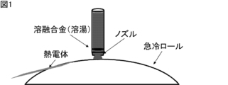
- the method for producing a thermoelectric element of the present invention includes the steps of producing a plate-shaped thermoelectric element containing a thermoelectric material having the anomalous Nernst effect using a liquid quenching method, and heat-treating the thermoelectric element, the liquid quenching method including a melt spinning method (single roll method), a twin roll method, or a strip casting method, the step of producing the thermoelectric element having an Eu (Euler) number in the liquid quenching method being in the range of 0.001 to 0.04, and the step of heat-treating the thermoelectric element heat-treating the thermoelectric element at a temperature of 450° C.
- Liquid quenching methods include melt spinning (single roll method), twin roll method, or strip casting method.
- thermoelectric material has a high proportion of ordered phases, that is, a state in which the thermoelectric material has a high degree of ordering (for example, a uniform structure with an average crystal grain size in the longitudinal direction of 10 ⁇ m or less), can be achieved, which leads to an increase in the anomalous Nernst coefficient in the process of heat treating the thermoelectric element described below.
- thermoelectric element is heat-treated, thereby obtaining a thermoelectric body.
- thermoelectric body of the present invention makes it possible to manufacture a thermoelectric body with high thermoelectromotive force.
- thermoelectric device of the present invention has, for example, the following structure:
- thermoelectric device of Structural Example 1 of the present invention has a structure in which a plurality of sheets made of thermoelectric material are laminated and joined by welding, soldering, conductive adhesive, etc.
- the plurality of sheets made of thermoelectric material may be connected to each other by metal wires, metal foils, etc. containing copper, aluminum, etc.
- thermoelectric device of the second structural example of the present invention has a structure in which a thermoelectric body is wound around a heat source (e.g., a heating body, a cooling body, etc.).
- the thermoelectric body may be wound in a spiral shape, a concentric shape, or a shape that combines a spiral shape and a concentric shape with respect to the heat source.
- thermoelectric device of the present invention preferably further comprises a heat dissipation member.
- the electromotive force of the thermoelectric device can be increased by closely adhering a highly thermally conductive sheet as a heat dissipation member between the thermoelectric body of the present invention and a heating body, which is an example of an object to which the thermoelectric body of the present invention is attached.
- the electromotive force of the thermoelectric device can be further increased by attaching a heat dissipation member to the surface of the thermoelectric device located opposite the heating body.
- thermoelectric body is manufactured by the manufacturing method of a thermoelectric body of the present invention.
- the thermoelectric body is cut and processed into sheets to manufacture a plurality of sheets made of the thermoelectric body.
- the plurality of sheets made of the thermoelectric body are then laminated while being joined by welding, soldering, a conductive adhesive, or the like to manufacture a thermoelectric device having a structure in which a plurality of sheets made of the thermoelectric body are laminated.
- the plurality of sheets made of the thermoelectric body may be connected to each other by a metal wire, a metal foil, or the like containing copper, aluminum, or the like.
- thermoelectric elements of Examples 1 to 7 were produced in the following manner.
- thermoelectric body of Comparative Example 2 was manufactured in the same manner as the thermoelectric bodies of Examples 1 to 7, except that the step of heat treating the thermoelectric body was not carried out.
- thermoelectric element of Comparative Example 3 was produced in the same manner as the thermoelectric elements of Examples 1 to 7, except that the thermoelectric element was heat-treated at 300° C. for 2 hours in the step of heat-treating the thermoelectric element.
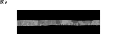
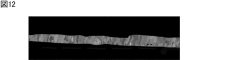
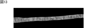
- ⁇ Average crystal grain size> A field emission scanning electron microscope (FE-SEM) manufactured by JEOL was used to observe the cross section of the thermoelectric body by using a backscattered electron image. Specifically, a resin structure was prepared by embedding the thermoelectric body in a resin. The obtained resin structure was then polished so that a cross section along the longitudinal direction (the pouring direction in the melt spinning method) and the thickness direction of the thermoelectric body was exposed, thereby preparing a measurement sample. The measurement sample is not limited to the above-mentioned one, as long as the cross section along the longitudinal direction and the thickness direction of the thermoelectric body can be observed. Next, the cross section along the longitudinal direction and the thickness direction of the thermoelectric body exposed in the measurement sample was observed with the above-mentioned field emission scanning electron microscope, and multiple images of the cross section were taken.
- FE-SEM field emission scanning electron microscope
- FIG. 4 is an image showing a cross section of a measurement sample of the thermoelectric body of Example 1.
- FIG. 5 is an image showing a cross section of a measurement sample of the thermoelectric body of Example 2.
- FIG. 6 is an image showing a cross section of a measurement sample of the thermoelectric body of Example 3.
- FIG. 7 is an image showing a cross section of a measurement sample of the thermoelectric body of Example 4.
- FIG. 8 is an image showing a cross section of a measurement sample of the thermoelectric body of Example 5.
- FIG. 9 is an image showing a cross section of a measurement sample of the thermoelectric body of Example 6.
- FIG. 10 is an image showing a cross section of a measurement sample of the thermoelectric body of Example 7.
- the electromotive force was measured in the presence of a magnetic field in the range of -2 T or more and +2 T or less (20 Oe/sec) by a superconducting magnet, and in the process from +2 T to +1 T, every 0.2 T was held for 1200 seconds, in the process from +1 T to -1 T, every 0.1 T was held for 1200 seconds, and in the process from -1 T to -2 T, every 0.2 T was held for 1200 seconds.
- thermoelectric elements of Examples 5 to 7 which satisfy both of the following: (2-1) Regarding the peak intensity measured by X-ray diffraction, the (111) peak intensity is 1.1 or more and 2.3 or less when the (220) peak intensity is set to 100; and (2-2) When the entire cross section along the longitudinal direction and thickness direction of the thermoelectric material is viewed, the average crystal grain size in the longitudinal direction is 14 ⁇ m or more and 35 ⁇ m or less, the anomalous Nernst coefficient of the thermoelectric material was 3 ⁇ V/K or more, which was very high.
- thermoelectric elements of Examples 1 to 7 can realize thermoelectric elements with high thermoelectromotive force.
- thermoelectric material of Comparative Example 1 which satisfied (1-2) above but did not satisfy (1-1), had a low anomalous Nernst coefficient of 1.5 ⁇ V/K compared to the thermoelectric materials of Examples 1 to 7.
- thermoelectric material of Comparative Example 3 which does not satisfy either (1-1) or (1-2) above, had a low anomalous Nernst coefficient of 2.4 ⁇ V/K compared to the thermoelectric materials of Examples 1 to 7.
- thermoelectric body thermoelectric element
- melt spinning method single roll method
- twin roll method twin roll method
- thermoelectric material having an anomalous Nernst effect;
- the shape is plate-like,
- the peak intensity of (111) is 1.1 or more when the peak intensity of (220) is set to 100;
- a thermoelectric material characterized in that, when viewing an entire cross section along the longitudinal direction and a thickness direction perpendicular to the longitudinal direction, the average crystal grain size in the longitudinal direction of the thermoelectric material is 9.6 ⁇ m or more.
- thermoelectric element according to ⁇ 1> wherein, when viewed in the cross section along the longitudinal direction and the thickness direction, for one principal surface and the other principal surface facing each other in the thickness direction, a ratio of an average crystal grain size in the longitudinal direction of the thermoelectric material at a position on the one principal surface side to an average crystal grain size in the longitudinal direction of the thermoelectric material at a position on the other principal surface side is 0.6 or less.
- thermoelectric element having a plate shape, the thermoelectric element including a thermoelectric material having the anomalous Nernst effect, by a liquid quenching method; and heat treating the thermoelectric element.
- the liquid quenching method includes a melt spinning method (single roll method), a twin roll method, or a strip casting method,
- the Eu (Euler) number in the liquid quenching method is set to a range of 0.001 or more and 0.04 or less
- a method for producing a thermoelectric body wherein in the step of heat treating the thermoelectric element, the thermoelectric element is heat treated at a temperature of 450°C or higher and 900°C or lower.
- thermoelectric device comprising the thermoelectric body according to ⁇ 1> or ⁇ 2>.
- thermoelectric device comprising the step of producing a thermoelectric body by the method for producing a thermoelectric body according to ⁇ 3>.
Landscapes
- Powder Metallurgy (AREA)
Priority Applications (2)
| Application Number | Priority Date | Filing Date | Title |
|---|---|---|---|
| JP2024514746A JPWO2024147216A1 (https=) | 2023-01-05 | 2023-09-26 | |
| CN202380014198.6A CN118715889A (zh) | 2023-01-05 | 2023-09-26 | 热电体、热电体的制造方法、热电设备和热电设备的制造方法 |
Applications Claiming Priority (4)
| Application Number | Priority Date | Filing Date | Title |
|---|---|---|---|
| JP2023000721 | 2023-01-05 | ||
| JP2023-000721 | 2023-01-05 | ||
| JP2023008180 | 2023-01-23 | ||
| JP2023-008180 | 2023-01-23 |
Publications (1)
| Publication Number | Publication Date |
|---|---|
| WO2024147216A1 true WO2024147216A1 (ja) | 2024-07-11 |
Family
ID=91803804
Family Applications (1)
| Application Number | Title | Priority Date | Filing Date |
|---|---|---|---|
| PCT/JP2023/034903 Ceased WO2024147216A1 (ja) | 2023-01-05 | 2023-09-26 | 熱電体、熱電体の製造方法、熱電デバイス、及び、熱電デバイスの製造方法 |
Country Status (2)
| Country | Link |
|---|---|
| JP (1) | JPWO2024147216A1 (https=) |
| WO (1) | WO2024147216A1 (https=) |
Citations (4)
| Publication number | Priority date | Publication date | Assignee | Title |
|---|---|---|---|---|
| WO2020129835A1 (ja) * | 2018-12-20 | 2020-06-25 | 日本電気株式会社 | 熱電変換素子 |
| JP2021145116A (ja) * | 2020-03-13 | 2021-09-24 | 国立大学法人 東京大学 | ワイル反強磁性体粉末およびそれを用いた熱電変換素子 |
| JP2022129848A (ja) * | 2021-02-25 | 2022-09-06 | 国立大学法人東北大学 | 磁性材料、積層体及び積層体の製造方法並びに熱電変換素子及び磁気センサ |
| WO2023277028A1 (ja) * | 2021-06-30 | 2023-01-05 | 株式会社村田製作所 | 熱電体、熱電体の製造方法、熱電デバイス、及び、熱電デバイスの製造方法 |
Family Cites Families (2)
| Publication number | Priority date | Publication date | Assignee | Title |
|---|---|---|---|---|
| JP3647420B2 (ja) * | 2002-04-30 | 2005-05-11 | 株式会社Neomax | 急冷合金の製造方法 |
| JP6593453B2 (ja) * | 2015-11-30 | 2019-10-23 | 日本製鉄株式会社 | 金属薄帯の製造装置及びそれを用いた金属薄帯の製造方法 |
-
2023
- 2023-09-26 JP JP2024514746A patent/JPWO2024147216A1/ja active Pending
- 2023-09-26 WO PCT/JP2023/034903 patent/WO2024147216A1/ja not_active Ceased
Patent Citations (4)
| Publication number | Priority date | Publication date | Assignee | Title |
|---|---|---|---|---|
| WO2020129835A1 (ja) * | 2018-12-20 | 2020-06-25 | 日本電気株式会社 | 熱電変換素子 |
| JP2021145116A (ja) * | 2020-03-13 | 2021-09-24 | 国立大学法人 東京大学 | ワイル反強磁性体粉末およびそれを用いた熱電変換素子 |
| JP2022129848A (ja) * | 2021-02-25 | 2022-09-06 | 国立大学法人東北大学 | 磁性材料、積層体及び積層体の製造方法並びに熱電変換素子及び磁気センサ |
| WO2023277028A1 (ja) * | 2021-06-30 | 2023-01-05 | 株式会社村田製作所 | 熱電体、熱電体の製造方法、熱電デバイス、及び、熱電デバイスの製造方法 |
Also Published As
| Publication number | Publication date |
|---|---|
| JPWO2024147216A1 (https=) | 2024-07-11 |
Similar Documents
| Publication | Publication Date | Title |
|---|---|---|
| KR102641049B1 (ko) | 고강도·고도전성 구리 합금 판재 및 그 제조 방법 | |
| KR100601413B1 (ko) | 연자기 특성이 우수한 Fe기 비정질 합금 박대, 이를사용하여 제조한 철심 및 이들에 사용되는 급랭 응고 박대제조용 모합금 | |
| EP2650885A1 (en) | Method for producing an aluminium electric wire for an automobile | |
| EP3521457A1 (en) | Soft magnetic alloy and magnetic device | |
| JP6984799B1 (ja) | 純銅板、銅/セラミックス接合体、絶縁回路基板 | |
| CN108463568B (zh) | 铜合金线材及铜合金线材的制造方法 | |
| JP4211318B2 (ja) | フィルドスクッテルダイト系合金、その製造方法および熱電変換素子 | |
| JP7718401B2 (ja) | Fe基ナノ結晶合金薄帯の製造方法、磁心の製造方法 | |
| WO2023277028A1 (ja) | 熱電体、熱電体の製造方法、熱電デバイス、及び、熱電デバイスの製造方法 | |
| WO2024147216A1 (ja) | 熱電体、熱電体の製造方法、熱電デバイス、及び、熱電デバイスの製造方法 | |
| Eickemeyer et al. | Textured Ni–7.5 at.% W substrate tapes for YBCO-coated conductors | |
| TWI904461B (zh) | 純銅材、絕緣基板、電子裝置 | |
| CN108698935B (zh) | 铜-陶瓷复合物 | |
| JP5617521B2 (ja) | 希薄銅合金材料を用いたエナメル線の製造方法 | |
| JP7281359B2 (ja) | コイル部品及びその製造方法 | |
| CN118715889A (zh) | 热电体、热电体的制造方法、热电设备和热电设备的制造方法 | |
| JP5354906B2 (ja) | 立方体集合組織を有するニッケルベースの半製品及びその製造方法 | |
| JP7277721B2 (ja) | 酸化物超電導バルク導体、及び、その製造方法 | |
| JP5353213B2 (ja) | 熱電材料、熱電材料の製造方法 | |
| JP7793982B2 (ja) | 銅合金、銅合金塑性加工材、電子・電気機器用部品、端子、バスバー、リードフレーム、放熱基板 | |
| US20180026170A1 (en) | Thermoelectric material and method for producing thermoelectric material | |
| JP7594355B2 (ja) | 構造物及び回路基板 | |
| WO2025105254A1 (ja) | 銅合金、銅合金塑性加工材、電子・電気機器用部品、フレキシブルデバイス用部品、放熱用部品、金属シール材 | |
| JP3466758B2 (ja) | ほう素を含有する金属酸化物線材、及び金属酸化物線材の製造方法 | |
| JP2001107160A (ja) | 高温高圧用恒電気抵抗合金およびその製造法ならびにセンサ |
Legal Events
| Date | Code | Title | Description |
|---|---|---|---|
| WWE | Wipo information: entry into national phase |
Ref document number: 2024514746 Country of ref document: JP |
|
| WWE | Wipo information: entry into national phase |
Ref document number: 202380014198.6 Country of ref document: CN |
|
| 121 | Ep: the epo has been informed by wipo that ep was designated in this application |
Ref document number: 23914705 Country of ref document: EP Kind code of ref document: A1 |
|
| NENP | Non-entry into the national phase |
Ref country code: DE |
|
| 122 | Ep: pct application non-entry in european phase |
Ref document number: 23914705 Country of ref document: EP Kind code of ref document: A1 |