WO2024142878A1 - 合金材料およびコンタクトプローブ - Google Patents
合金材料およびコンタクトプローブ Download PDFInfo
- Publication number
- WO2024142878A1 WO2024142878A1 PCT/JP2023/044187 JP2023044187W WO2024142878A1 WO 2024142878 A1 WO2024142878 A1 WO 2024142878A1 JP 2023044187 W JP2023044187 W JP 2023044187W WO 2024142878 A1 WO2024142878 A1 WO 2024142878A1
- Authority
- WO
- WIPO (PCT)
- Prior art keywords
- alloy material
- weight
- contact
- plunger
- probe
- Prior art date
- Legal status (The legal status is an assumption and is not a legal conclusion. Google has not performed a legal analysis and makes no representation as to the accuracy of the status listed.)
- Ceased
Links
Images








Classifications
-
- C—CHEMISTRY; METALLURGY
- C22—METALLURGY; FERROUS OR NON-FERROUS ALLOYS; TREATMENT OF ALLOYS OR NON-FERROUS METALS
- C22C—ALLOYS
- C22C5/00—Alloys based on noble metals
- C22C5/06—Alloys based on silver
-
- C—CHEMISTRY; METALLURGY
- C22—METALLURGY; FERROUS OR NON-FERROUS ALLOYS; TREATMENT OF ALLOYS OR NON-FERROUS METALS
- C22C—ALLOYS
- C22C30/00—Alloys containing less than 50% by weight of each constituent
- C22C30/02—Alloys containing less than 50% by weight of each constituent containing copper
-
- C—CHEMISTRY; METALLURGY
- C22—METALLURGY; FERROUS OR NON-FERROUS ALLOYS; TREATMENT OF ALLOYS OR NON-FERROUS METALS
- C22C—ALLOYS
- C22C5/00—Alloys based on noble metals
- C22C5/04—Alloys based on a platinum group metal
-
- G—PHYSICS
- G01—MEASURING; TESTING
- G01R—MEASURING ELECTRIC VARIABLES; MEASURING MAGNETIC VARIABLES
- G01R1/00—Details of instruments or arrangements of the types included in groups G01R5/00 - G01R13/00 and G01R31/00
- G01R1/02—General constructional details
- G01R1/06—Measuring leads; Measuring probes
- G01R1/067—Measuring probes
Definitions
- the alloy material according to the present invention is characterized in that it contains at least one of a group of trace elements consisting of nickel (Ni), tungsten (W), titanium (Ti), cobalt (Co), aluminum (Al), tin (Sn) and iridium (Ir) in a total amount ranging from 0.01% by weight to 3.0% by weight.
- a group of trace elements consisting of nickel (Ni), tungsten (W), titanium (Ti), cobalt (Co), aluminum (Al), tin (Sn) and iridium (Ir) in a total amount ranging from 0.01% by weight to 3.0% by weight.
- the probe 2 is a cross-sectional view showing the configuration of the main part of the probe unit according to one embodiment of the present invention.
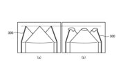
- the probe 2 is formed using a conductive material and includes a first plunger 21 that contacts an electrode of the semiconductor integrated circuit 100 when testing the semiconductor integrated circuit 100, a second plunger 22 that contacts an electrode of a circuit board 200 equipped with a test circuit, and a coil spring 23 that is provided between the first plunger 21 and the second plunger 22 and connects the first plunger 21 and the second plunger 22 so that they can move forward and backward.
- the first plunger 21, the second plunger 22, and the coil spring 23 that constitute the probe 2 have the same axis.
- the probe holder 3 is formed using an insulating material such as resin, machinable ceramic, or silicon, and is formed by stacking a first member 31 located on the upper side of FIG. 2 and a second member 32 located on the lower side.
- the first member 31 and the second member 32 are each formed with the same number of holder holes 33 and 34 for accommodating a plurality of probes 2, and the holder holes 33 and 34 that accommodate the probes 2 are formed so that their axes coincide with each other.
- the positions at which the holder holes 33 and 34 are formed are determined according to the wiring pattern of the semiconductor integrated circuit 100.
- the present invention should not be limited to only the above-mentioned embodiment.
- a contact probe has been explained as an example, but the alloy material of the present invention can be applied to any component for electrical or electronic equipment that comes into contact with a component containing Sn. In this case, at least the part of the component that comes into contact with the component needs to be made of the alloy material of the present invention.
Landscapes
- Chemical & Material Sciences (AREA)
- Engineering & Computer Science (AREA)
- Materials Engineering (AREA)
- Mechanical Engineering (AREA)
- Metallurgy (AREA)
- Organic Chemistry (AREA)
- Physics & Mathematics (AREA)
- General Physics & Mathematics (AREA)
- Measuring Leads Or Probes (AREA)
- Conductive Materials (AREA)
Priority Applications (3)
| Application Number | Priority Date | Filing Date | Title |
|---|---|---|---|
| JP2024567410A JPWO2024142878A1 (https=) | 2022-12-28 | 2023-12-11 | |
| CN202380088649.0A CN120418460A (zh) | 2022-12-28 | 2023-12-11 | 合金材料及接触式探针 |
| KR1020257020731A KR20250114061A (ko) | 2022-12-28 | 2023-12-11 | 합금 재료 및 콘택트 프로브 |
Applications Claiming Priority (2)
| Application Number | Priority Date | Filing Date | Title |
|---|---|---|---|
| JP2022-211785 | 2022-12-28 | ||
| JP2022211785 | 2022-12-28 |
Publications (1)
| Publication Number | Publication Date |
|---|---|
| WO2024142878A1 true WO2024142878A1 (ja) | 2024-07-04 |
Family
ID=91717504
Family Applications (1)
| Application Number | Title | Priority Date | Filing Date |
|---|---|---|---|
| PCT/JP2023/044187 Ceased WO2024142878A1 (ja) | 2022-12-28 | 2023-12-11 | 合金材料およびコンタクトプローブ |
Country Status (5)
| Country | Link |
|---|---|
| JP (1) | JPWO2024142878A1 (https=) |
| KR (1) | KR20250114061A (https=) |
| CN (1) | CN120418460A (https=) |
| TW (1) | TWI874046B (https=) |
| WO (1) | WO2024142878A1 (https=) |
Citations (8)
| Publication number | Priority date | Publication date | Assignee | Title |
|---|---|---|---|---|
| JPS61281837A (ja) * | 1985-06-07 | 1986-12-12 | Tanaka Kikinzoku Kogyo Kk | 装飾品用白金合金 |
| JPH03100159A (ja) * | 1989-09-12 | 1991-04-25 | Agency Of Ind Science & Technol | 光輝ある黒色に着色した白金合金とその着色法 |
| JPH11217638A (ja) * | 1997-11-27 | 1999-08-10 | Kyocera Corp | 銀合金 |
| JP2001040438A (ja) * | 1999-07-29 | 2001-02-13 | Kyocera Corp | 装飾用銀合金 |
| JP2001131654A (ja) * | 1999-10-29 | 2001-05-15 | Kyocera Corp | 銀合金 |
| US20170241004A1 (en) * | 2014-11-13 | 2017-08-24 | C. Hafner Gmbh + Co. Kg | Amorphous solidifying precious metal alloy based on precious metals |
| JP2017145496A (ja) * | 2016-02-19 | 2017-08-24 | 日本発條株式会社 | 合金材料、コンタクトプローブおよび接続端子 |
| CN114318048A (zh) * | 2021-12-16 | 2022-04-12 | 镇江市镇特合金材料有限公司 | 一种高焊接性能的导电瓦块用铜合金及其制备方法 |
Family Cites Families (5)
| Publication number | Priority date | Publication date | Assignee | Title |
|---|---|---|---|---|
| TW201009850A (en) * | 2008-08-28 | 2010-03-01 | King Yuan Electronics Co Ltd | An alloy material for electrical contact and probe thereof |
| CN103249852A (zh) * | 2010-12-09 | 2013-08-14 | 株式会社德力本店 | 电气/电子材料 |
| JP4878401B1 (ja) | 2011-05-17 | 2012-02-15 | 石福金属興業株式会社 | プローブピン用材料、プローブピン及びその製造方法 |
| WO2013099682A1 (ja) | 2011-12-27 | 2013-07-04 | 株式会社徳力本店 | 電気・電子機器用のPd合金 |
| WO2014049874A1 (ja) * | 2012-09-28 | 2014-04-03 | 株式会社徳力本店 | 電気・電子機器用途のAg‐Pd‐Cu‐Co合金 |
-
2023
- 2023-12-11 KR KR1020257020731A patent/KR20250114061A/ko active Pending
- 2023-12-11 CN CN202380088649.0A patent/CN120418460A/zh active Pending
- 2023-12-11 JP JP2024567410A patent/JPWO2024142878A1/ja active Pending
- 2023-12-11 WO PCT/JP2023/044187 patent/WO2024142878A1/ja not_active Ceased
- 2023-12-14 TW TW112148790A patent/TWI874046B/zh active
Patent Citations (8)
| Publication number | Priority date | Publication date | Assignee | Title |
|---|---|---|---|---|
| JPS61281837A (ja) * | 1985-06-07 | 1986-12-12 | Tanaka Kikinzoku Kogyo Kk | 装飾品用白金合金 |
| JPH03100159A (ja) * | 1989-09-12 | 1991-04-25 | Agency Of Ind Science & Technol | 光輝ある黒色に着色した白金合金とその着色法 |
| JPH11217638A (ja) * | 1997-11-27 | 1999-08-10 | Kyocera Corp | 銀合金 |
| JP2001040438A (ja) * | 1999-07-29 | 2001-02-13 | Kyocera Corp | 装飾用銀合金 |
| JP2001131654A (ja) * | 1999-10-29 | 2001-05-15 | Kyocera Corp | 銀合金 |
| US20170241004A1 (en) * | 2014-11-13 | 2017-08-24 | C. Hafner Gmbh + Co. Kg | Amorphous solidifying precious metal alloy based on precious metals |
| JP2017145496A (ja) * | 2016-02-19 | 2017-08-24 | 日本発條株式会社 | 合金材料、コンタクトプローブおよび接続端子 |
| CN114318048A (zh) * | 2021-12-16 | 2022-04-12 | 镇江市镇特合金材料有限公司 | 一种高焊接性能的导电瓦块用铜合金及其制备方法 |
Also Published As
| Publication number | Publication date |
|---|---|
| CN120418460A (zh) | 2025-08-01 |
| KR20250114061A (ko) | 2025-07-28 |
| JPWO2024142878A1 (https=) | 2024-07-04 |
| TW202449182A (zh) | 2024-12-16 |
| TWI874046B (zh) | 2025-02-21 |
Similar Documents
| Publication | Publication Date | Title |
|---|---|---|
| US9804198B2 (en) | Alloy material, contact probe, and connection terminal | |
| JP6647075B2 (ja) | 合金材料、コンタクトプローブおよび接続端子 | |
| US7091734B2 (en) | Electroconductive contact unit | |
| JP6550457B2 (ja) | 合金材料、コンタクトプローブおよび接続端子 | |
| JP6728057B2 (ja) | 合金材料、コンタクトプローブおよび接続端子 | |
| JP4216823B2 (ja) | プローブピン及び該ブロ−ブビンを備えたブロ−ブカ−ド | |
| JP2012230117A (ja) | 電気接触子及び電気部品用ソケット | |
| JP2001337110A (ja) | プローブピンおよびプローブカード | |
| WO2024142878A1 (ja) | 合金材料およびコンタクトプローブ | |
| JP7008529B2 (ja) | 検査装置用リード線、リード線装着部品及び検査用治具 | |
| TWI305839B (en) | Contact-making apparatus and method for production of at least one contact element of a contact-making apparatus | |
| US20250297344A1 (en) | Alloy material for probe pins | |
| US20240167125A1 (en) | Alloy material for probe pins | |
| KR102934049B1 (ko) | 석출경화 공정을 이용한 스프링 콘택트 핀의 제조 방법 | |
| JPH05203670A (ja) | コンタクトプローブ | |
| JP2009216413A (ja) | 金属プローブ | |
| CN117015625A (zh) | 探测针用合金材料 | |
| JP5154011B2 (ja) | フレキシブルフラットケーブル | |
| WO2024014231A1 (ja) | プローブ装置 | |
| HK1210232B (en) | Alloy material, contact probe, and connection terminal |
Legal Events
| Date | Code | Title | Description |
|---|---|---|---|
| 121 | Ep: the epo has been informed by wipo that ep was designated in this application |
Ref document number: 23911659 Country of ref document: EP Kind code of ref document: A1 |
|
| WWE | Wipo information: entry into national phase |
Ref document number: 2024567410 Country of ref document: JP |
|
| WWE | Wipo information: entry into national phase |
Ref document number: 1020257020731 Country of ref document: KR |
|
| WWE | Wipo information: entry into national phase |
Ref document number: 202380088649.0 Country of ref document: CN |
|
| WWP | Wipo information: published in national office |
Ref document number: 1020257020731 Country of ref document: KR |
|
| NENP | Non-entry into the national phase |
Ref country code: DE |
|
| WWP | Wipo information: published in national office |
Ref document number: 202380088649.0 Country of ref document: CN |
|
| 122 | Ep: pct application non-entry in european phase |
Ref document number: 23911659 Country of ref document: EP Kind code of ref document: A1 |