WO2024142768A1 - 固体電解コンデンサ、および固体電解コンデンサの製造方法 - Google Patents
固体電解コンデンサ、および固体電解コンデンサの製造方法 Download PDFInfo
- Publication number
- WO2024142768A1 WO2024142768A1 PCT/JP2023/043226 JP2023043226W WO2024142768A1 WO 2024142768 A1 WO2024142768 A1 WO 2024142768A1 JP 2023043226 W JP2023043226 W JP 2023043226W WO 2024142768 A1 WO2024142768 A1 WO 2024142768A1
- Authority
- WO
- WIPO (PCT)
- Prior art keywords
- layer
- solid electrolyte
- surface roughness
- electrolyte layer
- electrolytic capacitor
- Prior art date
- Legal status (The legal status is an assumption and is not a legal conclusion. Google has not performed a legal analysis and makes no representation as to the accuracy of the status listed.)
- Ceased
Links
Images


Classifications
-
- H—ELECTRICITY
- H01—ELECTRIC ELEMENTS
- H01G—CAPACITORS; CAPACITORS, RECTIFIERS, DETECTORS, SWITCHING DEVICES, LIGHT-SENSITIVE OR TEMPERATURE-SENSITIVE DEVICES OF THE ELECTROLYTIC TYPE
- H01G9/00—Electrolytic capacitors, rectifiers, detectors, switching devices, light-sensitive or temperature-sensitive devices; Processes of their manufacture
- H01G9/004—Details
- H01G9/022—Electrolytes; Absorbents
- H01G9/025—Solid electrolytes
- H01G9/028—Organic semiconducting electrolytes, e.g. TCNQ
-
- H—ELECTRICITY
- H01—ELECTRIC ELEMENTS
- H01G—CAPACITORS; CAPACITORS, RECTIFIERS, DETECTORS, SWITCHING DEVICES, LIGHT-SENSITIVE OR TEMPERATURE-SENSITIVE DEVICES OF THE ELECTROLYTIC TYPE
- H01G9/00—Electrolytic capacitors, rectifiers, detectors, switching devices, light-sensitive or temperature-sensitive devices; Processes of their manufacture
- H01G9/004—Details
- H01G9/04—Electrodes or formation of dielectric layers thereon
- H01G9/048—Electrodes or formation of dielectric layers thereon characterised by their structure
- H01G9/055—Etched foil electrodes
Definitions
- the present invention relates to a solid electrolytic capacitor that is made by stacking multiple capacitor elements formed using a conductive adhesive layer.
- Patent Document 1 and Patent Document 2 describe a solid electrolytic capacitor.
- This solid electrolytic capacitor includes multiple capacitor elements. Each of the multiple capacitor elements functions as an individual solid electrolytic capacitor.
- the average surface roughness of the solid electrolyte layer in the solid electrolytic capacitor of Patent Document 1 is specified to be in the range of 0.1 ⁇ m to 30 ⁇ m. Furthermore, the surface roughness Ra of the conductive polymer layer (solid electrolyte layer) in the solid electrolytic capacitor of Patent Document 2 is specified to be in the range of 0.3 ⁇ m to 5 ⁇ m. Increasing the contact area between the solid electrolyte layer and the cathode lead layer in this way improves the adhesive strength between the solid electrolyte layer and the cathode lead layer (including the silver layer).
- the method for manufacturing this solid electrolytic capacitor includes a capacitor element forming process and a cathode lead layer forming process.
- a capacitor element forming process a flat membrane-shaped capacitor element is formed in which a dielectric layer and a solid electrolyte layer are sequentially formed on the surface of a flat membrane-shaped anode electrode foil.
- a cathode lead layer forming process a cathode lead layer is formed that is laminated on the solid electrolyte layer in the capacitor element.
- FIG. 1 is a side cross-sectional view of a capacitor element constituting a solid electrolytic capacitor according to a first embodiment.
- FIG. 2 is an enlarged view of a portion of a cross section of the capacitor element according to the first embodiment.
- FIG. 3(A) is a graph showing the surface roughness of the solid electrolyte layer of the solid electrolytic capacitor according to the first embodiment
- FIG. 3(B) is a graph showing the surface roughness of the cathode lead layer of the solid electrolytic capacitor according to the first embodiment.
- FIG. 4 is a table showing characteristics of the solid electrolytic capacitor based on the surface roughness ratio according to the first embodiment.
- the surface vicinity of the electrode foil 111 has many holes.
- the surface vicinity of the electrode foil 111 is in a porous state (porous body).
- a dielectric layer 112 is formed on the electrode foil 111.
- the dielectric layer 112 is preferably made of an oxide film of the electrode foil 111.
- the dielectric layer 112 is formed by oxidizing the electrode foil 111 in an aqueous solution containing boric acid, phosphoric acid, adipic acid, or their sodium salts, ammonium salts, or the like.
- the thickness of the dielectric layer 112 is preferably 10 nm or more and 100 nm or less.
- the inner layer is formed by a method of forming a polymer film of poly(3,4-ethylenedioxythiophene) or the like on the surface of the dielectric layer 112 using an electrolyte solution that is the base for forming the solid electrolyte layer 113, for example, a treatment liquid containing a monomer such as 3,4-ethylenedioxythiophene, or a method of applying a dispersion of a polymer such as poly(3,4-ethylenedioxythiophene) to the surface of the dielectric part and drying it.
- the surface where the solid electrolyte layer 113 and the conductive adhesive layer 114 come into contact has a surface roughness. More specifically, the surface of the solid electrolyte layer 113 on the conductive adhesive layer 114 side where the solid electrolyte layer 113 comes into contact with the conductive adhesive layer 114 is the first surface. Also, the surface of the solid electrolyte layer 113 on the solid electrolyte layer 113 side where the solid electrolyte layer 113 comes into contact with the conductive adhesive layer 114 is the second surface.
- the first surface has a first surface roughness Ra1.
- the second surface has a second surface roughness Ra2.
- the surface roughness in the present invention is not the macroscopic surface roughness as shown in the prior art, but the local surface roughness. In other words, it is the surface roughness calculated by defining an even smaller area than the area in which the macroscopic surface roughness is measured as shown in the prior art.
- the method for calculating the surface roughness is as follows.
- Step 5 Using the standard deviation obtained in step 4 as the surface roughness, calculate the surface roughness within a 300 ⁇ m square area.
- Fig. 4 shows the results of determining the ratio (Ra1/Ra2) of the first surface roughness Ra1 of the solid electrolyte layer 113 to the second surface roughness Ra2 of the conductive adhesive layer 114 (pattern A, pattern B, pattern C, pattern D).
- the ESR degradation coefficient and the life of solid electrolytic capacitors including capacitor element 11 were compared for each pattern of the conductive adhesive layer 114.
- the ESR degradation coefficient is calculated as follows.
- the capacitor element 11 is left in a thermostatic chamber at 145° C. In this state, the capacitor element 11 is taken out before being left in the chamber (initial state), after 500 hours from the initial state, and every 500 hours thereafter.
- the ESR of the capacitor element 11 is measured in a room temperature atmosphere (Agilent E4980A). The measurement frequency is 100 kHz.
- the slope of the linear regression equation for the standing time is calculated as the ESR degradation coefficient.
- the ESR degradation coefficient increases, the ESR increases. In other words, if the ESR degradation coefficient is small, the increase in ESR is suppressed.
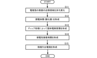
- Fig. 6 is a flowchart showing a flow of a process for forming the capacitor element according to the first embodiment.
- the area (surface layer) near the surface of the electrode foil 111 is made porous (S11).
- the porosity is achieved, for example, by etching the surface.
- the dielectric layer 112 is formed (S12).
- the dielectric layer 112 is formed by oxidizing the surface of the electrode foil 111 and the surface of the porous body.
- a solid electrolyte layer 113 is attached to the surface of the electrode foil 111 and the surface of the porous body by dipping (S13).
- the electrolyte solution that will be the base of the solid electrolyte layer 113 is placed in a tank.
- the electrode foil 111 is hung from the top of the tank. At this time, the electrode foil 111 is hung so that the second end 11EG2 is on the bottom side. In this state, the electrode foil 111 is immersed in the electrolyte solution. After being immersed for a predetermined time, the electrode foil 111 is pulled out of the electrolyte solution. After being pulled out, it is left for a predetermined time and the electrolyte solution is dried. This series of operations, immersion in the electrolyte solution, pulling up, and drying, is repeated a predetermined number of times as necessary.
- the conductive adhesive layer 114 is formed on the solid electrolyte layer 113 (S14).
- the conductive adhesive layer 114 is formed by applying carbon paste to the surface on which the solid electrolyte layer 113 is formed and drying it.
- the ratio of the first surface roughness Ra1 of the conductive adhesive layer 114 to the second surface roughness Ra2 of the solid electrolyte layer 113 is controlled to be 1.0 to 2.0.
- the cathode lead electrode 115 is formed on the conductive adhesive layer 114 (S15).
- the cathode lead electrode 115 is formed by applying a conductive paste to the surface on which the conductive adhesive layer 114 is formed and then drying it.
- the insulating resin body 40 is mainly made of resin and may contain a filler.
- resins include epoxy resin, phenol resin, polyimide resin, silicone resin, polyamide resin, and liquid crystal polymer.
- the resin may be in either solid or liquid form. It is preferred that the corners are rounded by barrel polishing after resin sealing.
- preferred fillers include silica particles, alumina particles, and metal particles. The maximum diameter of the filler is preferably 30 ⁇ m or more and 40 ⁇ m or less. It is more preferred that the material contains silica particles in addition to solid epoxy resin and phenol resin.
- the adhesive area between the conductive adhesive layer 114 and the solid electrolyte layer 113 is increased.
- the adhesive strength between the cathode lead electrode 115, the conductive adhesive layer 114, and the solid electrolyte layer 113 is improved.
- the increase in ESR can be suppressed. Therefore, the life of the solid electrolytic capacitor 1 equipped with the capacitor element 11 is improved.
- the solid electrolytic capacitor 1 can achieve high reliability.
- Fig. 9 is a side cross-sectional view of the solid electrolytic capacitor according to the second embodiment.
- the capacitor element assembly 10 is sealed with an insulating resin body 40.
- the insulating resin body 40 has a generally rectangular parallelepiped shape with a top surface 401, a bottom surface 402, a first end surface 403, and a second end surface 404.
- the capacitor element 11 like the first and second embodiments, comprises a flat film-shaped electrode foil, a dielectric layer, and a solid electrolyte layer.
- the cathode lead layer comprises a conductive adhesive layer 114 and a cathode lead electrode 115.
- the cathode lead electrode 115 uses a film-shaped conductor such as a metal foil.
- the multiple capacitor elements 11 and the multiple cathode lead layers are alternately stacked so that their flat film surfaces are parallel and overlap when viewed from above.
- the capacitor element stack 100 is sealed with insulating resin 50. More specifically, as shown in FIG. 10, the insulating resin 50 covers the capacitor element stack 100 except for the first ends 10E1 of the multiple capacitor elements 11 (first ends 10E1 of the electrode foils 111) and the first ends 20E1 of the multiple cathode lead electrodes 115.
- the external electrode 62 covers the second end of the insulating resin 50 (the first end 20E1 of the cathode lead electrode 115).
- the external electrode 62 is connected to the first ends 20E1 of the multiple cathode lead electrodes 115.
Landscapes
- Engineering & Computer Science (AREA)
- Power Engineering (AREA)
- Chemical & Material Sciences (AREA)
- Chemical Kinetics & Catalysis (AREA)
- Electrochemistry (AREA)
- Microelectronics & Electronic Packaging (AREA)
- Electrolytic Production Of Metals (AREA)
Priority Applications (1)
| Application Number | Priority Date | Filing Date | Title |
|---|---|---|---|
| JP2024567349A JPWO2024142768A1 (https=) | 2022-12-27 | 2023-12-04 |
Applications Claiming Priority (2)
| Application Number | Priority Date | Filing Date | Title |
|---|---|---|---|
| JP2022210009 | 2022-12-27 | ||
| JP2022-210009 | 2022-12-27 |
Publications (1)
| Publication Number | Publication Date |
|---|---|
| WO2024142768A1 true WO2024142768A1 (ja) | 2024-07-04 |
Family
ID=91717398
Family Applications (1)
| Application Number | Title | Priority Date | Filing Date |
|---|---|---|---|
| PCT/JP2023/043226 Ceased WO2024142768A1 (ja) | 2022-12-27 | 2023-12-04 | 固体電解コンデンサ、および固体電解コンデンサの製造方法 |
Country Status (2)
| Country | Link |
|---|---|
| JP (1) | JPWO2024142768A1 (https=) |
| WO (1) | WO2024142768A1 (https=) |
Citations (3)
| Publication number | Priority date | Publication date | Assignee | Title |
|---|---|---|---|---|
| JP2000049054A (ja) * | 1998-05-22 | 2000-02-18 | Matsushita Electric Ind Co Ltd | 電解コンデンサおよびその製造方法 |
| JP2009170897A (ja) * | 2007-12-21 | 2009-07-30 | Sanyo Electric Co Ltd | 固体電解コンデンサ |
| JP2010108971A (ja) * | 2008-10-28 | 2010-05-13 | Nippon Zeon Co Ltd | 電気化学素子用電極の製造方法および電気化学素子 |
-
2023
- 2023-12-04 JP JP2024567349A patent/JPWO2024142768A1/ja active Pending
- 2023-12-04 WO PCT/JP2023/043226 patent/WO2024142768A1/ja not_active Ceased
Patent Citations (3)
| Publication number | Priority date | Publication date | Assignee | Title |
|---|---|---|---|---|
| JP2000049054A (ja) * | 1998-05-22 | 2000-02-18 | Matsushita Electric Ind Co Ltd | 電解コンデンサおよびその製造方法 |
| JP2009170897A (ja) * | 2007-12-21 | 2009-07-30 | Sanyo Electric Co Ltd | 固体電解コンデンサ |
| JP2010108971A (ja) * | 2008-10-28 | 2010-05-13 | Nippon Zeon Co Ltd | 電気化学素子用電極の製造方法および電気化学素子 |
Also Published As
| Publication number | Publication date |
|---|---|
| JPWO2024142768A1 (https=) | 2024-07-04 |
Similar Documents
| Publication | Publication Date | Title |
|---|---|---|
| CN109791844B (zh) | 固体电解电容器 | |
| US11875950B2 (en) | Electrolytic capacitor | |
| JP7531117B2 (ja) | 電解コンデンサおよびその製造方法 | |
| US11881360B2 (en) | Electrolytic capacitor | |
| JP7065301B2 (ja) | 固体電解コンデンサおよびその製造方法 | |
| JP7792584B2 (ja) | 固体電解コンデンサ素子および固体電解コンデンサ | |
| WO2018066254A1 (ja) | 固体電解コンデンサ | |
| WO2018150886A1 (ja) | 固体電解コンデンサ及びその製造方法 | |
| WO2018066253A1 (ja) | 固体電解コンデンサ | |
| JP7029666B2 (ja) | 固体電解コンデンサ | |
| JP5623214B2 (ja) | 固体電解コンデンサ | |
| US12283438B2 (en) | Electrolytic capacitor | |
| WO2024142768A1 (ja) | 固体電解コンデンサ、および固体電解コンデンサの製造方法 | |
| US12424392B2 (en) | Electrolytic capacitor and method for manufacturing electrolytic capacitor | |
| US11984272B2 (en) | Solid electrolytic capacitor | |
| JP4953091B2 (ja) | コンデンサチップ及びその製造方法 | |
| CN102420053B (zh) | 固体电解电容器的制造方法及固体电解电容器 | |
| JP6865356B2 (ja) | 固体電解コンデンサ | |
| US12406814B2 (en) | Solid electrolytic capacitor element, solid electrolytic capacitor and method for producing same | |
| WO2023189222A1 (ja) | 電極箔、コンデンサ素子、および、固体電解コンデンサ | |
| CN112466667B (zh) | 固体电解电容器以及固体电解电容器的制造方法 | |
| JP4899758B2 (ja) | 固体電解コンデンサ用リードフレーム部材 | |
| JP4899759B2 (ja) | 固体電解コンデンサ用リードフレーム部材 | |
| WO2020137548A1 (ja) | 電解コンデンサおよびその製造方法 | |
| JP2025039520A (ja) | コンデンサ素子、固体電解コンデンサ、および固体電解コンデンサの製造方法 |
Legal Events
| Date | Code | Title | Description |
|---|---|---|---|
| 121 | Ep: the epo has been informed by wipo that ep was designated in this application |
Ref document number: 23911549 Country of ref document: EP Kind code of ref document: A1 |
|
| WWE | Wipo information: entry into national phase |
Ref document number: 2024567349 Country of ref document: JP |
|
| NENP | Non-entry into the national phase |
Ref country code: DE |
|
| 122 | Ep: pct application non-entry in european phase |
Ref document number: 23911549 Country of ref document: EP Kind code of ref document: A1 |