WO2024142672A1 - 積層セラミックコンデンサ - Google Patents
積層セラミックコンデンサ Download PDFInfo
- Publication number
- WO2024142672A1 WO2024142672A1 PCT/JP2023/041747 JP2023041747W WO2024142672A1 WO 2024142672 A1 WO2024142672 A1 WO 2024142672A1 JP 2023041747 W JP2023041747 W JP 2023041747W WO 2024142672 A1 WO2024142672 A1 WO 2024142672A1
- Authority
- WO
- WIPO (PCT)
- Prior art keywords
- internal electrode
- electrode layer
- dielectric
- opposing
- layer
- Prior art date
- Legal status (The legal status is an assumption and is not a legal conclusion. Google has not performed a legal analysis and makes no representation as to the accuracy of the status listed.)
- Ceased
Links
Images


Classifications
-
- H—ELECTRICITY
- H01—ELECTRIC ELEMENTS
- H01G—CAPACITORS; CAPACITORS, RECTIFIERS, DETECTORS, SWITCHING DEVICES, LIGHT-SENSITIVE OR TEMPERATURE-SENSITIVE DEVICES OF THE ELECTROLYTIC TYPE
- H01G4/00—Fixed capacitors; Processes of their manufacture
- H01G4/30—Stacked capacitors
-
- H—ELECTRICITY
- H01—ELECTRIC ELEMENTS
- H01G—CAPACITORS; CAPACITORS, RECTIFIERS, DETECTORS, SWITCHING DEVICES, LIGHT-SENSITIVE OR TEMPERATURE-SENSITIVE DEVICES OF THE ELECTROLYTIC TYPE
- H01G4/00—Fixed capacitors; Processes of their manufacture
- H01G4/002—Details
- H01G4/005—Electrodes
-
- H—ELECTRICITY
- H01—ELECTRIC ELEMENTS
- H01G—CAPACITORS; CAPACITORS, RECTIFIERS, DETECTORS, SWITCHING DEVICES, LIGHT-SENSITIVE OR TEMPERATURE-SENSITIVE DEVICES OF THE ELECTROLYTIC TYPE
- H01G4/00—Fixed capacitors; Processes of their manufacture
- H01G4/002—Details
- H01G4/005—Electrodes
- H01G4/012—Form of non-self-supporting electrodes
-
- H—ELECTRICITY
- H01—ELECTRIC ELEMENTS
- H01G—CAPACITORS; CAPACITORS, RECTIFIERS, DETECTORS, SWITCHING DEVICES, LIGHT-SENSITIVE OR TEMPERATURE-SENSITIVE DEVICES OF THE ELECTROLYTIC TYPE
- H01G4/00—Fixed capacitors; Processes of their manufacture
- H01G4/002—Details
- H01G4/018—Dielectrics
- H01G4/06—Solid dielectrics
- H01G4/08—Inorganic dielectrics
- H01G4/12—Ceramic dielectrics
-
- H—ELECTRICITY
- H01—ELECTRIC ELEMENTS
- H01G—CAPACITORS; CAPACITORS, RECTIFIERS, DETECTORS, SWITCHING DEVICES, LIGHT-SENSITIVE OR TEMPERATURE-SENSITIVE DEVICES OF THE ELECTROLYTIC TYPE
- H01G4/00—Fixed capacitors; Processes of their manufacture
- H01G4/002—Details
- H01G4/228—Terminals
- H01G4/232—Terminals electrically connecting two or more layers of a stacked or rolled capacitor
Definitions
- the internal electrode layers 15 are preferably made of a metal material such as Ni, Cu, Ag, Pd, an Ag-Pd alloy, or Au.
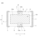
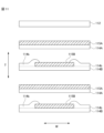
- FIG. 4 is a cross-sectional view taken along the first internal electrode layer 15A of the multilayer ceramic capacitor 1.
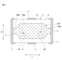
- FIG. 5 is a cross-sectional view taken along the second internal electrode layer 15B of the multilayer ceramic capacitor 1.
- the first internal electrode layer 15A has a first opposing portion 15Aa that is slightly smaller than the laminate 2 and has a substantially rectangular shape with each side spaced a fixed distance from the end face C and the side face B, and side extension portions 15Ab that extend from the first opposing portion 15Aa to both side faces B.
- the first opposing portion 15Aa includes a connection region JA that is a portion that is connected to the side drawn-out portion 15Ab.
- Figures 2 and 4 show the connection region JA of the first opposing portion 15Aa to which the side drawn-out portion 15Ab is connected.
- the first opposing portion 15Aa has two connection regions JA corresponding to the two side drawn-out portions 15Ab.
- the side lead portions 15Ab extending to the two opposing side surfaces B are exposed at the side surfaces B of the laminate 2 and are connected to the side surface external electrodes 4 provided on both side surfaces B in the width direction W of the laminate 2 .
- the length in the longitudinal direction L of the side lead portion 15Ab is shorter than the length in the longitudinal direction L of the first opposing portion 15Aa. In this way, by shortening the length in the longitudinal direction L of the side lead portion 15Ab, it is possible to suppress the intrusion of moisture from the outside, thereby improving the reliability of the multilayer ceramic capacitor.
- Figure 4 shows a configuration in which both of the two side lead portions 15Ab are shorter in the longitudinal direction L than the first opposing portion 15Aa.
- the end surface drawn-out portion 15Bb has a transition region where the length in the width direction W gradually decreases, and an extension region that extends from the transition region to the end surface C and has a length in the width direction W that is shorter than the length in the width direction of the second opposing portion 15Ba.
- Figure 5 shows a form in which both extension portions of the two end surface drawn-out portions 15Bb are shorter in the width direction W than the second opposing portion 15Ba.
- the outer layer portion 12 is a dielectric layer of a constant thickness disposed on the main surface A side of the inner layer portion 11.
- the outer layer portion 12 is made of the same material as the dielectric layer 14 of the inner layer portion 11.
- the thickness of the dielectric layer is not particularly limited, but is preferably 0.3 ⁇ m to 1.5 ⁇ m, and more preferably 0.5 ⁇ m to 1 ⁇ m.
- the laminate 2 consisting of the inner layer 11 and the outer layer 12 can be formed from 14 to 1,000 dielectric layers.
- End surface external electrode 3 End surface external electrodes 3 are disposed on both end surfaces C of the laminate 2. End surface drawn-out portions 15Bb of second internal electrode layers 15B are connected to the end surface external electrodes 3. The end surface external electrodes 3 cover not only the end surfaces C, but also parts of the main surfaces A and side surfaces B on the end surface C side.
- Side external electrodes 4 are disposed on both side surfaces B of the laminate 2.
- a side extension portion 15Ab of the first internal electrode layer 15A is connected to the side external electrodes 4.
- the side external electrodes 4 cover not only the side surfaces B but also a portion of the main surface A on the side surface B side.
- the end face external electrode 3 and the side face external electrode 4 can have a structure including, for example, a base electrode layer and a plating layer disposed on the base electrode layer.
- the thickness of the baked layer is preferably, for example, 3 ⁇ m or more and 70 ⁇ m or less.
- the baked layer may also be multiple layers.
- the conductive resin layer is formed by applying a conductive resin paste containing a thermosetting resin and a metal component onto a baking layer or a laminate, and then performing a heat treatment at a temperature of 250 to 550°C or higher to thermally cure the resin and form a conductive resin layer.
- the atmosphere during the heat treatment is preferably a N2 atmosphere.
- the thickness of the conductive resin layer at the center of end face C is preferably, for example, 10 ⁇ m or more and 150 ⁇ m or less.
- the conductive resin layer preferably contains a curing agent in addition to the thermosetting resin.
- a curing agent in addition to the thermosetting resin.
- various known compounds such as phenol-based, amine-based, acid anhydride-based, and imidazole-based compounds can be used as the curing agent for the epoxy resin.
- the metal contained in the conductive resin layer can be Ag, Cu, or an alloy of these.
- Metal powder with an Ag-coated surface can also be used.
- metal powder with an Ag-coated surface it is preferable to use Cu or Ni as the metal powder.
- Cu that has been treated to prevent oxidation can also be used.
- the reason for using Ag conductive metal powder as the conductive metal is that Ag has the lowest resistivity of all metals, making it suitable as an electrode material, and because Ag is a precious metal, it does not oxidize and has high resistance.
- the reason for using Ag-coated metal is that it is possible to make the base metal cheaper while maintaining the above-mentioned properties of Ag.
- the metal contained in the conductive resin layer is preferably contained in an amount of 35 vol% or more and 75 vol% or less relative to the total volume of the conductive resin.
- the shape of the metal contained in the conductive resin layer is not particularly limited.
- the conductive filler may be spherical, flat, etc.
- the average particle size of the metal contained in the conductive resin layer is not particularly limited, but can be, for example, about 0.3 ⁇ m or more and 10 ⁇ m or less.
- the plating layer preferably contains at least one metal selected from, for example, Cu, Ni, Sn, Pb, Au, Ag, Pd, Bi, or Zn, or an alloy containing the metal.
- the direct plating layer is preferably formed using Cu, which has good bonding properties with Ni.
- the thin film layer is formed by a thin film formation method such as sputtering or vapor deposition, and is a layer of 1 ⁇ m or less in thickness in which metal particles are deposited.
- the plating layer disposed on the base electrode layer contains, for example, at least one selected from Cu, Ni, Ag, Pd, Ag-Pd alloy, Au, etc.
- the plating layer may be formed of multiple layers. Preferably, it has a two-layer structure of Ni plating and Sn plating.
- the Ni plating layer can prevent the base electrode layer from being eroded by solder when mounting ceramic electronic components, and the Sn plating layer improves the wettability of the solder when mounting ceramic electronic components, making mounting easier.
- the thickness of each plating layer is preferably 2 ⁇ m or more and 15 ⁇ m or less.
- the internal electrode layers 15 communicate in the stacking direction T, and have through holes P into which a part of the dielectric constituting the dielectric layers 14 sandwiching the internal electrode layers 15 from the stacking direction T has entered. Inside the through holes P, columnar crystals of the dielectric are formed, which can increase the adhesion between the internal electrode layers 15 and the dielectric layers 14.
- the presence rate of the through holes P into which the dielectric has entered is higher in the connection region JA where the side drawn-out portion 15Ab of the first opposing portion 15Aa is connected than the center of the first opposing portion 15Aa and higher than the center of the side drawn-out portion 15Ab.
- the presence rate of the through holes P into which the dielectric has entered can be confirmed by polishing the end face C of the multilayer ceramic capacitor 1 parallel to the end face C to expose a cross section, and observing the cross section using a scanning electron microscope.
- the presence rate of the through holes P into which the dielectric has entered in the connection region JA is measured on a cross section polished to a position that is 1/2 the lengthwise dimension of the multilayer ceramic capacitor 1 so as to be perpendicular to the length direction L.
- the above cross section is divided into three regions so that the thickness dimension of the inner layer portion is divided into three equal parts.
- the field of view is specified so that the magnification is such that 15 layers of the first internal electrode layers 15A are included, with the end of one of the opposing parts of the first internal electrode layers 15A as the center.
- the SEM image is analyzed in the specified field of view of each region, and the existence rate of the through holes P into which the dielectric has penetrated is calculated by the following formula (1) based on the area of the first internal electrode layers 15A actually existing in the analysis range, the area of the through holes, and the area of the through holes P into which the dielectric has penetrated.
- Presence rate (%) of communicating holes P into which dielectric has entered (area of communicating holes P into which dielectric has entered/area of internal electrode layer+area of communicating holes) ⁇ 100 (1)
- the average of the measurements for 15 layers in each of the three regions is taken to determine the rate of presence of communicating holes P into which the dielectric has penetrated in the connection region JA.
- the rate of presence of the through holes P into which the dielectric has penetrated in the center of the first opposing portion 15Aa is measured on a cross section of the multilayer ceramic capacitor 1 that has been polished to a position perpendicular to the longitudinal direction L, which is 1/2 of the longitudinal dimension of the multilayer ceramic capacitor 1.
- the cross section is divided into three regions so that the thickness dimension of the inner layer portion is divided into three equal parts.
- the field of view is specified so that the magnification is such that 15 layers of the first internal electrode layer 15A are included, with the center of the first opposing portion 15Aa of the first internal electrode layer 15A as the center.
- the rate of presence of the through holes P into which the dielectric has penetrated in the center of the side drawn-out portion 15Ab is measured on a cross section of the multilayer ceramic capacitor 1 that has been polished to a position perpendicular to the length direction L, which is 1/2 the length direction dimension of the multilayer ceramic capacitor 1.
- the cross section is divided into three regions so that the thickness dimension of the inner layer portion is divided into three equal parts.
- the field of view is specified so that the magnification is such that 15 layers of the first internal electrode layer 15A are included, with the center of one of the side drawn-out portions 15Ab of the first internal electrode layer 15A as the center.
- the SEM image is analyzed within the specified field of view of each region, and the rate of presence of the through holes P into which the dielectric has penetrated is calculated based on the area of the first internal electrode layer 15A, the area of the through holes, and the area of the through holes P into which the dielectric has penetrated that are actually present in the analysis range, using the following formula (1).
- Presence rate (%) of communicating holes P into which dielectric has entered (area of communicating holes P into which dielectric has entered/area of internal electrode layer+area of communicating holes) ⁇ 100 (1)
- the average of the measurements for 15 layers in each of the three regions is taken to determine the rate of presence of communicating holes P into which the dielectric has penetrated in the side drawn-out portion 15Ab.
- the rate of occurrence of communicating holes P into which the dielectric has entered in the connection region JA is preferably 20% or more and 60% or less
- the rate of occurrence of communicating holes P into which the dielectric has entered in the central portion of the first opposing portion 15Aa is preferably 2% or more and 25% or less
- the rate of occurrence of communicating holes P into which the dielectric has entered in the central portion of the side draw-out portion 15Ab is preferably 2% or more and 25% or less.
- the interval T1 of the portion overlapping with the second internal electrode layer 15B in the connection region JA where the first opposing portion 15Aa and the side drawn portion 15Ab are joined when the first internal electrode layer 15A is viewed in a plane from the stacking direction T is longer than the interval T2 in the center of the first opposing portion 15Aa, and has a portion longer than the interval T3 in the side drawn portion 15Ab that does not overlap with the second internal electrode layer 15B when the first internal electrode layer 15A is viewed in a plane from the stacking direction T.
- the interval in the stacking direction T of the first internal electrode layer 15A can be measured at each portion by polishing the end face C of the multilayer ceramic capacitor 1 parallel to the end face C to expose the cross section and observing the cross section using a scanning electron microscope, similar to the measurement of the presence rate of the through holes P into which the dielectric has entered. Specifically, the distance T1 between the overlapping portions of the second internal electrode layer 15B in the connection region JA is measured on a cross section of the multilayer ceramic capacitor 1 polished perpendicular to the longitudinal direction L to a position that is 1/2 the longitudinal dimension of the multilayer ceramic capacitor 1.
- the cross section is divided into three regions so that the thickness dimension of the inner layer portion is divided into three equal parts, and the dimension T1 is measured at 20 points in each region using a scanning electron microscope (SEM). Finally, the average value is taken to be the distance T1 between the overlapping portions of the second internal electrode layer 15B in the connection region JA. Similarly to the measurement of T1, the thickness dimension of the inner layer portion is divided into three regions in the above cross section, and the dimension of T2 is measured at 20 points in each region using a scanning electron microscope (SEM). Finally, the average value is taken as the distance T2 in the center of the first opposing portion 15Aa.
- the spacing T1 of the portion overlapping with the second internal electrode layer 15B in the connection region JA be 1.2 ⁇ m or more and 6.0 ⁇ m or less
- the spacing T2 at the center of the first opposing portion 15Aa be 1.1 ⁇ m or more and 5.0 ⁇ m or less
- the spacing T3 in the side extension portion 15Ab that does not overlap with the second internal electrode layer 15B when the first internal electrode layer 15A is viewed in a plane from the stacking direction T be 0.8 ⁇ m or more and 5.0 ⁇ m or less.
- a multi-terminal type multilayer ceramic capacitor having three or more external electrodes is known, but in such a multi-terminal multilayer ceramic capacitor, the overlapping state between the multiple internal electrode layers and the multiple dielectric layers tends to be more complicated than that of a normal two-terminal ceramic capacitor.
- the internal electrode layers of a multi-terminal multilayer ceramic capacitor often do not have a simple rectangular shape, and the overlapping state between the internal electrode layers and the dielectric layers becomes more complicated. In this case, during the pressing process before firing the laminate, an area where pressure is difficult to apply is generated, and the adhesion force near that area is weakened.
- the adhesion force is weakened near the boundary between the opposing electrode portion and the lead portion, which is likely to be a mutation point in the overlapping state between the internal electrode layer and the dielectric layer, and delamination is likely to occur.
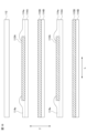
- FIG. 6 is a flow chart illustrating a method for manufacturing the multilayer ceramic capacitor 1.
- 7 to 16 are process diagrams illustrating the manufacturing method of the multilayer ceramic capacitor 1, while FIGS. 9 to 12 show the arrangement of the ceramic pastes 114a, 114b according to the first embodiment, and FIGS. 13 to 16 show the arrangement of the ceramic pastes 114a, 114b according to the second embodiment.
- a first internal electrode layer pattern 115A that will become the first internal electrode layer 15A is formed from a conductive paste on a first ceramic green sheet 114A that will become the dielectric layer 14c.
- a sintering aid is sprayed at the position where the through holes are to be formed.
- Mn, Si, etc. can be used as the sintering aid.
- the first internal electrode layer pattern 115A has a shape in which a plurality of first internal electrode layers 15A are continuous in the width direction W but discontinuous in the length direction L.
- a second internal electrode layer pattern 115B which will become the second internal electrode layer 15B is formed from a conductive paste on a second ceramic green sheet 114B which will become the dielectric layer 14c.
- the second internal electrode layer pattern 115B has a shape in which a plurality of second internal electrode layers 15B are continuous in the length direction L but discontinuous in the width direction W.
- Ceramic green sheets are strip-shaped sheets made by forming a ceramic slurry containing ceramic powder, binder and solvent onto a carrier film using a die coater, gravure coater, microgravure coater, etc.
- the first internal electrode layer pattern 115A and the second internal electrode layer pattern 115B are formed by printing, for example, screen printing, gravure printing, letterpress printing, etc.
- a ceramic paste 114b to become the dielectric layer 14a is applied onto the sheet on which the second internal electrode layer pattern 115B is formed on the second ceramic green sheet 114B shown in Fig. 8.
- the thickness of the dielectric layer 14a is 0.4 to 0.8 times the thickness of the dielectric layer 14c.
- the ceramic paste 114b fills the entire portion of the second ceramic green sheet 114B where the second internal electrode layer pattern 115B is not arranged, and is further arranged so as to overlap the portions corresponding to both side edges in the width direction W of the second opposing portion 15Ba of the second internal electrode layer pattern 115B.
- Ceramic paste 114a and ceramic paste 114b are applied by printing, such as screen printing, gravure printing, letterpress printing, etc.
- the ceramic paste may have a different component ratio from the dielectric material used to make the ceramic green sheets, may have the same component ratio, or may contain different components.
- FIG. 11 is a diagram for explaining the stacking state of the laminate 2 in the WT cross section at the center in the longitudinal direction L.
- Fig. 11 shows a schematic state in which the multiple laminated ceramic green sheets are separated from each other. The same is true for Figs. 12, 15, and 16.
- a sheet in which a first internal electrode layer pattern 115A and ceramic paste 114a are arranged on a first ceramic green sheet 114A shown in FIG. 9, and a sheet in which a second internal electrode layer pattern 115B and ceramic paste 114b are arranged on a second ceramic green sheet 114B shown in FIG. 10 are alternately laminated.
- the ceramic paste 114b forms the dielectric layer 14a.
- FIG. 12 is a diagram illustrating the stacked state of the laminate 2 at the LT cross section at the center in the width direction W.
- the first internal electrode layer pattern 115A and the second internal electrode layer pattern 115B both extend in the length direction L with a constant spacing in the stacking direction T.
- the ceramic paste 114a forms the dielectric layer 14b.
- outer layer ceramic green sheets 112 which will become the outer layer 12, are stacked on both sides of the stack in the stacking direction T.
- end surface external electrodes 3 are formed on both end surfaces C of the laminate 2
- side surface external electrodes 4 are formed on both side surfaces B of the laminate 2
- An end surface drawn portion 15Bb of the second internal electrode layer 15B is connected to the end surface external electrode 3.
- the end surface external electrode 3 is formed so as to cover not only the end surface C but also a part of the main surface A and the side surface B on the end surface C side.
- a side surface lead portion 15Ab of the first internal electrode layer 15A is connected to the side surface external electrode 4.
- the side surface external electrode 4 is formed so as to cover not only the side surface B but also a part of the main surface A on the side surface B side.
- step S7 The laminate is then heated in a nitrogen atmosphere for a predetermined time at the set firing temperature, thereby baking the external electrodes onto the laminate 2, and the laminated ceramic capacitor 1 shown in FIG.
- the laminated chip is subjected to a binder removal process and a firing process to form the element part (laminate 2).
- the conductive paste layer and the green sheet for the dielectric layer are co-sintered by the firing process to form the internal electrode layer 15 and the dielectric layer 14, respectively.
- the conditions for the binder removal process can be determined according to the type of organic binder contained in the green sheet and the conductive paste layer.
- the firing process can be performed at a temperature at which the laminated chip is sufficiently densified. The firing temperature depends on the materials of the dielectric and the internal electrode layer, but is preferably 900°C to 1400°C.
- the multilayer ceramic capacitor 1 manufactured in this manner has a spacing in the stacking direction T between adjacent first internal electrode layers 15A in the stacking direction T, such that when the first internal electrode layer 15A is viewed in a plane from the stacking direction T, the spacing T1 of the portion of the first opposing portion 15Aa that overlaps with the second internal electrode layer 15B in the connection area JA where the side lead portion 15Ab is joined is longer than the spacing T2 of the center of the first opposing portion 15Aa, and is longer than the spacing T3 of the side lead portion 15Ab that does not overlap with the second internal electrode layer 15B when the first internal electrode layer 15A is viewed in a plane from the stacking direction T.
- the distance T1 is larger than the other distances T2 and T3, so this portion is more likely to be subjected to pressure from the dielectric layer 14.
- some of the dielectric that forms the dielectric layer 14 is more likely to enter the through holes P of the internal electrode layer 15, making it easier for columnar crystals to form due to the dielectric, and making it possible to increase the adhesion between the internal electrode layer 15 and the dielectric layer 14.
- the presence rate of the through holes P in the first internal electrode layer into which the dielectric has penetrated is higher in the connection region JA where the side lead portion 15Ab of the first opposing portion 15Aa is connected than in the center of the first opposing portion 15Aa, and is also higher than in the center of the side lead portion 15Ab, so that the adhesion with the dielectric layer 14 can be increased in the connection region JA.
- the first internal electrode layer 15A and the second internal electrode layer 15B of the laminate 2 extend in the length direction L with a constant spacing between them in the stacking direction T.
- a plating layer is provided.
- a Ni plating layer and a Sn plating layer are formed on the baked layer.
- the Ni plating layer and the Sn plating layer are formed in this order by, for example, barrel plating. In this manner, the multilayer ceramic capacitor 1 can be obtained.
- the second embodiment differs from the first embodiment in the ranges of ceramic pastes 114a and 114b that are placed on the ceramic green sheets on which the internal electrode layer patterns are formed.
- FIG. 13 is a diagram showing a state in which a ceramic paste 114a is arranged on a sheet in which a first internal electrode layer pattern 115A is formed on a first ceramic green sheet 114A in the second embodiment, and corresponds to FIG. 9 in the first embodiment.
- the ceramic paste 114a fills the entire portion of the first ceramic green sheet 114A where the first internal electrode layer pattern 115A is not arranged, and is arranged so as to overlap both side edges of the first opposing portion 15Aa in the length direction L and both side edges of the first opposing portion 15Aa in the width direction W, excluding the connection region JA of the first opposing portion.
- Figure 13 shows a form in which the ceramic paste 114a is not placed in the portion that becomes the side extension portion 15Ab of the first internal electrode layer 15A, but this is not limited to this, and the ceramic paste 114a may also be placed in the portion that becomes the side extension portion 15Ab of the first internal electrode layer 15A, and in the connection region JA where the first opposing portion 15Aa and the side extension portion 15Ab are joined.
- FIG. 14 is a diagram showing a state in which a ceramic paste 114b is arranged on a sheet in which a second internal electrode layer pattern 115B is formed on a second ceramic green sheet 114B in the second embodiment, and corresponds to FIG. 10 in the first embodiment.
- the ceramic paste 114b fills the entire portion of the second ceramic green sheet 114B where the second internal electrode layer pattern 115B is not arranged, and is arranged so as to overlap portions corresponding to both side edges in the width direction W of the second opposing portion 15Ba of the second internal electrode layer pattern 115B, and portions at both ends in the length direction L of the second opposing portion 15Ba and corresponding to four locations corresponding to both ends in the width direction W.
- the ceramic paste 114b is not placed in a portion that will become the end surface drawn-out portion 15Bb of the second internal electrode layer 15B.
- FIGS. 15 and 16 show a state in which a sheet in which a first internal electrode layer pattern 115A and ceramic paste 114a are arranged on a first ceramic green sheet 114A shown in FIG. 13, and a sheet in which a second internal electrode layer pattern 115B and ceramic paste 114b that will become a dielectric layer 14a are arranged on a second ceramic green sheet 114B shown in FIG. 14 are alternately laminated.
- the ceramic paste 114b overlaps both ends of the second internal electrode layer pattern 115B in the width direction W.
- the ceramic paste 114b forms the dielectric layer 14a.
- the ceramic paste 114a overlaps both ends of the first internal electrode layer pattern 115A in the length direction L.
- the ceramic paste 114a forms the dielectric layer 14b. This form corresponds to FIG. 11 of the first embodiment, and a cross section corresponding to FIG. 2 of the first embodiment is formed.
- the presence rate of the through holes P into which the dielectric has penetrated in the second internal electrode layer 15B is higher in the connection region JB where the end face drawn-out portion 15Bb of the second opposing portion 15Ba is connected than in the center of the second opposing portion 15Ba, and is higher than in the center of the end face drawn-out portion 15Bb, thereby improving the adhesion with the dielectric layer 14.
- the cross-sectional shape shown in FIG. 15 also corresponds to FIG. 11 of the first embodiment, and a cross section corresponding to FIG. 2 of the first embodiment is formed, so that the adhesion with the dielectric layer 14 can also be improved in the connection region JA where the first opposing portion 15Aa and the side face drawn-out portion 15Ab are joined.
- the above describes an embodiment of the present invention, but the present invention is not limited to the embodiment, and can be embodied in various forms without departing from the gist of the present invention.
- the present invention includes the following combinations.
- a laminate including an inner layer portion in which a plurality of dielectric layers and internal electrode layers are alternately laminated, the laminate having two main surfaces opposed to each other in a lamination direction, two end faces opposed to each other in a length direction intersecting with the lamination direction, and two side surfaces opposed to each other in a width direction intersecting with the lamination direction and the length direction; an external electrode connected to the internal electrode layer on at least one of the side surface and the end surface of the laminate;
- a multilayer ceramic capacitor comprising:
- the internal electrode layer includes a first internal electrode layer and a second internal electrode layer, the first internal electrode layer and the second internal electrode layer include opposing portions that overlap each other in a plan view from the stacking direction, and lead-out portions that are led from the opposing portions to the end faces or the side faces of the laminate and do not overlap each other in a plan view from the stacking direction, the internal electrode layers are connected in the stacking direction and have through holes into which the dielectric constituting the dielectric layers penetrate,
- a multilayer ceramic capacitor wherein
- the internal electrode layer includes the first internal electrode layer and the second internal electrode layer, the first internal electrode layer includes a first opposing portion opposing the second internal electrode layer via the dielectric layer, and a side surface drawn-out portion drawn out from the first opposing portion to the side surface of the laminate, the second internal electrode layer includes a second opposing portion opposing the first internal electrode layer via the dielectric layer, and an end surface drawn portion drawn from the opposing portion to the two end surfaces of the laminate, the internal electrode layers are connected in the stacking direction and have through holes into which the dielectric constituting the dielectric layers penetrate,
- the multilayer ceramic capacitor according to ⁇ 1> wherein the presence rate of the communicating holes in the first internal electrode layer is higher in a connection region of the first opposing portion to which the side drawn-out portion is connected than in a central portion of the first opposing portion and is also higher than in a central portion of the side drawn-out portion.
- ⁇ 3> A multilayer ceramic capacitor according to ⁇ 2>, in which, in the spacing in the stacking direction between the first internal electrode layers adjacent to each other in the stacking direction, the spacing T1 in the connection region that overlaps with the second internal electrode layer when the first internal electrode layer is viewed in a plane from the stacking direction is longer than the spacing T2 in the center of the first opposing portion, and has a portion that is longer than the spacing T3 in the side lead-out portion that does not overlap with the second internal electrode layer when the first internal electrode layer is viewed in a plane from the stacking direction.
- the first internal electrode layer includes two side surface drawn-out portions drawn out to two side surfaces of the laminate opposed to each other in the width direction,
- ⁇ 5> A multilayer ceramic capacitor according to any one of ⁇ 2> to ⁇ 4>, in which the length of the side lead portion in the longitudinal direction of the first internal electrode layer is shorter than the length of the first opposing portion in the longitudinal direction.
- ⁇ 6> A multilayer ceramic capacitor according to any one of ⁇ 2> to ⁇ 5>, in which the length in the longitudinal direction of the two side extension portions of the first internal electrode layer that are extended to the two side surfaces of the laminate that face each other in the width direction is shorter than the length in the longitudinal direction of the first opposing portion.
- ⁇ 7> A multilayer ceramic capacitor according to any one of ⁇ 2> to ⁇ 6>, in which the width direction length of the end face extraction portion in the second internal electrode layer is shorter than the width direction length of the first opposing portion.
- ⁇ 8> A multilayer ceramic capacitor according to any one of ⁇ 2> to ⁇ 7>, in which in the second internal electrode layer, the widthwise length of the two end face extraction portions is shorter than the widthwise length of the first opposing portion.
- the laminate includes the inner layer portion in which the dielectric layers and the internal electrode layers are alternately laminated, and the laminate has two main surfaces opposed to each other in the lamination direction, two end faces opposed to each other in a length direction intersecting with the lamination direction, and two side surfaces opposed to each other in a width direction intersecting with the lamination direction and the length direction; external electrodes connected to the internal electrode layers on the side surfaces and the end surfaces of the laminate;
- a multilayer ceramic capacitor comprising:
- the internal electrode layer includes the first internal electrode layer and the second internal electrode layer, the first internal electrode layer includes a first opposing portion opposing the second internal electrode layer via the dielectric layer, and a side surface drawn-out portion drawn out from the first opposing portion to the side surface of the laminate, the second internal electrode layer includes a second opposing portion opposing the first internal electrode layer via the dielectric layer, and an end surface drawn portion drawn from the opposing portion to the two end surfaces of the laminate, the internal electrode layers are connected in the stacking direction and have through holes into which the dielectric constituting
Landscapes
- Engineering & Computer Science (AREA)
- Power Engineering (AREA)
- Manufacturing & Machinery (AREA)
- Microelectronics & Electronic Packaging (AREA)
- Chemical & Material Sciences (AREA)
- Ceramic Engineering (AREA)
- Inorganic Chemistry (AREA)
- Fixed Capacitors And Capacitor Manufacturing Machines (AREA)
- Ceramic Capacitors (AREA)
Priority Applications (4)
| Application Number | Priority Date | Filing Date | Title |
|---|---|---|---|
| KR1020257017115A KR20250093555A (ko) | 2022-12-28 | 2023-11-21 | 적층 세라믹 콘덴서 |
| CN202380089409.2A CN120380559A (zh) | 2022-12-28 | 2023-11-21 | 层叠陶瓷电容器 |
| JP2024567290A JPWO2024142672A1 (https=) | 2022-12-28 | 2023-11-21 | |
| US19/251,873 US20250329494A1 (en) | 2022-12-28 | 2025-06-27 | Multilayer ceramic capacitor |
Applications Claiming Priority (2)
| Application Number | Priority Date | Filing Date | Title |
|---|---|---|---|
| JP2022212596 | 2022-12-28 | ||
| JP2022-212596 | 2022-12-28 |
Related Child Applications (1)
| Application Number | Title | Priority Date | Filing Date |
|---|---|---|---|
| US19/251,873 Continuation US20250329494A1 (en) | 2022-12-28 | 2025-06-27 | Multilayer ceramic capacitor |
Publications (1)
| Publication Number | Publication Date |
|---|---|
| WO2024142672A1 true WO2024142672A1 (ja) | 2024-07-04 |
Family
ID=91717078
Family Applications (1)
| Application Number | Title | Priority Date | Filing Date |
|---|---|---|---|
| PCT/JP2023/041747 Ceased WO2024142672A1 (ja) | 2022-12-28 | 2023-11-21 | 積層セラミックコンデンサ |
Country Status (5)
| Country | Link |
|---|---|
| US (1) | US20250329494A1 (https=) |
| JP (1) | JPWO2024142672A1 (https=) |
| KR (1) | KR20250093555A (https=) |
| CN (1) | CN120380559A (https=) |
| WO (1) | WO2024142672A1 (https=) |
Citations (11)
| Publication number | Priority date | Publication date | Assignee | Title |
|---|---|---|---|---|
| JPS5822728U (ja) * | 1981-08-04 | 1983-02-12 | 株式会社村田製作所 | 積層セラミツクコンデンサ |
| JPH0268429U (https=) * | 1988-11-15 | 1990-05-24 | ||
| JPH02265226A (ja) * | 1989-03-03 | 1990-10-30 | Philips Gloeilampenfab:Nv | キャパシタおよびその製造方法 |
| JPH0897071A (ja) * | 1994-09-29 | 1996-04-12 | Kyocera Corp | 積層型磁器コンデンサ |
| JPH1022172A (ja) * | 1996-06-29 | 1998-01-23 | Taiyo Yuden Co Ltd | 積層電子部品とその製造方法 |
| JP2008091400A (ja) * | 2006-09-29 | 2008-04-17 | Tdk Corp | 積層セラミックコンデンサ及びその製造方法 |
| JP2008294298A (ja) * | 2007-05-25 | 2008-12-04 | Murata Mfg Co Ltd | 電子部品 |
| JP2015159140A (ja) * | 2014-02-21 | 2015-09-03 | 京セラ株式会社 | コンデンサ |
| JP2022053271A (ja) * | 2020-09-24 | 2022-04-05 | 株式会社村田製作所 | 積層セラミックコンデンサ |
| JP2022075191A (ja) * | 2020-11-06 | 2022-05-18 | 株式会社村田製作所 | 積層セラミックコンデンサ及び積層セラミックコンデンサの製造方法 |
| JP2022104530A (ja) * | 2020-12-28 | 2022-07-08 | サムソン エレクトロ-メカニックス カンパニーリミテッド. | 積層型キャパシタ及びその実装基板 |
Family Cites Families (1)
| Publication number | Priority date | Publication date | Assignee | Title |
|---|---|---|---|---|
| JP2016127262A (ja) | 2014-12-26 | 2016-07-11 | 太陽誘電株式会社 | 貫通型積層セラミックコンデンサ |
-
2023
- 2023-11-21 KR KR1020257017115A patent/KR20250093555A/ko active Pending
- 2023-11-21 WO PCT/JP2023/041747 patent/WO2024142672A1/ja not_active Ceased
- 2023-11-21 JP JP2024567290A patent/JPWO2024142672A1/ja active Pending
- 2023-11-21 CN CN202380089409.2A patent/CN120380559A/zh active Pending
-
2025
- 2025-06-27 US US19/251,873 patent/US20250329494A1/en active Pending
Patent Citations (11)
| Publication number | Priority date | Publication date | Assignee | Title |
|---|---|---|---|---|
| JPS5822728U (ja) * | 1981-08-04 | 1983-02-12 | 株式会社村田製作所 | 積層セラミツクコンデンサ |
| JPH0268429U (https=) * | 1988-11-15 | 1990-05-24 | ||
| JPH02265226A (ja) * | 1989-03-03 | 1990-10-30 | Philips Gloeilampenfab:Nv | キャパシタおよびその製造方法 |
| JPH0897071A (ja) * | 1994-09-29 | 1996-04-12 | Kyocera Corp | 積層型磁器コンデンサ |
| JPH1022172A (ja) * | 1996-06-29 | 1998-01-23 | Taiyo Yuden Co Ltd | 積層電子部品とその製造方法 |
| JP2008091400A (ja) * | 2006-09-29 | 2008-04-17 | Tdk Corp | 積層セラミックコンデンサ及びその製造方法 |
| JP2008294298A (ja) * | 2007-05-25 | 2008-12-04 | Murata Mfg Co Ltd | 電子部品 |
| JP2015159140A (ja) * | 2014-02-21 | 2015-09-03 | 京セラ株式会社 | コンデンサ |
| JP2022053271A (ja) * | 2020-09-24 | 2022-04-05 | 株式会社村田製作所 | 積層セラミックコンデンサ |
| JP2022075191A (ja) * | 2020-11-06 | 2022-05-18 | 株式会社村田製作所 | 積層セラミックコンデンサ及び積層セラミックコンデンサの製造方法 |
| JP2022104530A (ja) * | 2020-12-28 | 2022-07-08 | サムソン エレクトロ-メカニックス カンパニーリミテッド. | 積層型キャパシタ及びその実装基板 |
Also Published As
| Publication number | Publication date |
|---|---|
| KR20250093555A (ko) | 2025-06-24 |
| US20250329494A1 (en) | 2025-10-23 |
| JPWO2024142672A1 (https=) | 2024-07-04 |
| CN120380559A (zh) | 2025-07-25 |
Similar Documents
| Publication | Publication Date | Title |
|---|---|---|
| US11062848B2 (en) | Multilayer ceramic electronic component | |
| CN114334449B (zh) | 层叠陶瓷电容器 | |
| US12340950B2 (en) | Multilayer ceramic capacitor | |
| CN114334443B (zh) | 层叠陶瓷电容器 | |
| US11735369B2 (en) | Multilayer ceramic capacitor | |
| CN115881434B (zh) | 层叠陶瓷电容器 | |
| US10361032B2 (en) | Ceramic capacitor including first, second, and third external electrodes wrapping around side and principal surfaces | |
| JP2022077451A (ja) | 積層セラミックコンデンサ | |
| WO2024142672A1 (ja) | 積層セラミックコンデンサ | |
| JP7751261B2 (ja) | 積層セラミックコンデンサ | |
| WO2024142679A1 (ja) | 積層セラミックコンデンサ | |
| JP2022163423A (ja) | 積層セラミックコンデンサ | |
| JP7852745B2 (ja) | 積層セラミックコンデンサ | |
| US20260128216A1 (en) | Multilayer ceramic electronic component | |
| JP2024162476A (ja) | 積層セラミックコンデンサ | |
| JP7784015B2 (ja) | 積層型電子部品 | |
| WO2025150229A1 (ja) | 積層セラミックコンデンサ | |
| WO2024247445A1 (ja) | 積層セラミックコンデンサ | |
| JP2019179820A (ja) | 積層セラミックコンデンサ | |
| WO2024034240A1 (ja) | 積層セラミック電子部品 | |
| KR20250170137A (ko) | 적층 세라믹 전자부품 | |
| WO2024018718A1 (ja) | 積層セラミック電子部品および積層セラミック電子部品の実装構造 | |
| CN121532842A (zh) | 层叠陶瓷电容器 | |
| CN121336274A (zh) | 层叠陶瓷电子部件 | |
| WO2024018720A1 (ja) | 積層セラミックコンデンサ及び積層セラミックコンデンサの製造方法 |
Legal Events
| Date | Code | Title | Description |
|---|---|---|---|
| 121 | Ep: the epo has been informed by wipo that ep was designated in this application |
Ref document number: 23911454 Country of ref document: EP Kind code of ref document: A1 |
|
| ENP | Entry into the national phase |
Ref document number: 20257017115 Country of ref document: KR Kind code of ref document: A |
|
| WWE | Wipo information: entry into national phase |
Ref document number: 2024567290 Country of ref document: JP |
|
| WWP | Wipo information: published in national office |
Ref document number: 1020257017115 Country of ref document: KR |
|
| WWE | Wipo information: entry into national phase |
Ref document number: 202380089409.2 Country of ref document: CN |
|
| WWP | Wipo information: published in national office |
Ref document number: 202380089409.2 Country of ref document: CN |
|
| NENP | Non-entry into the national phase |
Ref country code: DE |
|
| 122 | Ep: pct application non-entry in european phase |
Ref document number: 23911454 Country of ref document: EP Kind code of ref document: A1 |