WO2024142564A1 - フィルムコンデンサ - Google Patents
フィルムコンデンサ Download PDFInfo
- Publication number
- WO2024142564A1 WO2024142564A1 PCT/JP2023/037993 JP2023037993W WO2024142564A1 WO 2024142564 A1 WO2024142564 A1 WO 2024142564A1 JP 2023037993 W JP2023037993 W JP 2023037993W WO 2024142564 A1 WO2024142564 A1 WO 2024142564A1
- Authority
- WO
- WIPO (PCT)
- Prior art keywords
- electrode
- film
- width
- dielectric film
- slit
- Prior art date
- Legal status (The legal status is an assumption and is not a legal conclusion. Google has not performed a legal analysis and makes no representation as to the accuracy of the status listed.)
- Ceased
Links
Images


Classifications
-
- H—ELECTRICITY
- H01—ELECTRIC ELEMENTS
- H01G—CAPACITORS; CAPACITORS, RECTIFIERS, DETECTORS, SWITCHING DEVICES, LIGHT-SENSITIVE OR TEMPERATURE-SENSITIVE DEVICES OF THE ELECTROLYTIC TYPE
- H01G4/00—Fixed capacitors; Processes of their manufacture
- H01G4/32—Wound capacitors
Definitions
- the present invention relates to a film capacitor.
- One type of capacitor is a film capacitor, which is made of a wound or laminated dielectric film with an internal electrode layer made of a metal vapor deposition film on its surface.
- film capacitors have a self-healing property (the metal vapor deposition film scatters and restores insulation when an insulation defect is discharged).
- the present invention was made to solve the above problems, and aims to provide a film capacitor that can suppress the occurrence of short circuits.
- the film capacitor of the present invention will be described below. However, the present invention is not limited to the following configurations, and can be appropriately modified and applied within the scope of the present invention.
- the present invention also includes a combination of two or more of the individual preferred configurations of the present invention described below.
- the laminate may be a wound body in which the metallized film is wound in a laminated state.
- first metallized film 11 and the second metallized film 12 are shown spaced apart, but in an actual film capacitor, the first metallized film 11 and the second metallized film 12 are stacked together with no gaps.
- the film capacitor 1 shown in FIG. 1 further includes an external electrode 40 provided on an end face of the laminate 15 and electrically connected to the internal electrode layer 30.
- the external electrode 40 includes a first external electrode 41 provided on one end face of the laminate 15 and electrically connected to the first internal electrode layer 31, and a second external electrode 42 provided on the other end face of the laminate 15 and electrically connected to the second internal electrode layer 32.
- the first internal electrode layer 31 and the second internal electrode layer 32 face each other via the first dielectric film 21.
- the first dielectric film 21 and the second dielectric film 22 are laminated so that the other main surface of the first dielectric film 21 (the main surface on the side where the first internal electrode layer 31 is not provided) faces one main surface of the second dielectric film 22 (the main surface on the side where the second internal electrode layer 32 is provided).
- the first metallized film 11 and the second metallized film 12 may have different configurations, but preferably have the same configuration.
- the first dielectric film 21 and the second dielectric film 22 may have different configurations, but preferably have the same configuration.
- the first internal electrode layer 31 and the second internal electrode layer 32 may have different configurations, but preferably have the same configuration.
- the first internal electrode layer 31 is preferably provided on one main surface of the first dielectric film 21 so as to reach one side edge (the left side edge in FIG. 1, the upper side edge in FIG. 2) but not to reach the other side edge (the right side edge in FIG. 1, the lower side edge in FIG. 2).
- a first insulating margin 91 is present on the other side edge of one main surface of the first dielectric film 21, where the first internal electrode layer 31 is not provided.
- the thickness of the internal electrode layer 30 can be determined by observing a cross section of the metallized film 10 cut in the thickness direction using an electron microscope such as a field emission scanning electron microscope (FE-SEM).
- FE-SEM field emission scanning electron microscope
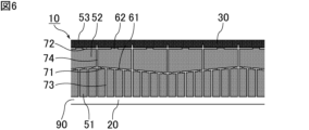
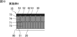
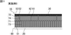
- the first internal electrode layer 31 includes a first electrode 51, a second electrode 52, a third electrode 53, a first connection portion 61, and a second connection portion 62.
- a first insulating margin 91 where the first internal electrode layer 31 is not provided may be present on the side edge of the first dielectric film 21 on the first electrode 51 side.
- a first slit 71 is provided between the first electrode 51 and the second electrode 52, and extends intermittently in the longitudinal direction of the dielectric film 20 (the left-right direction in FIG. 2).
- the first electrode 51 is connected to the second electrode 52 via a first connection portion 61 provided between the first slits 71.
- the first connection portion 61 has a fuse function.
- a second slit 72 is provided between the second electrode 52 and the third electrode 53, and extends intermittently in the longitudinal direction of the dielectric film 20.
- the second electrode 52 is connected to the third electrode 53 via a second connection portion 62 provided between the second slits 72.
- the second connection portion 62 may have a fuse function, but preferably does not have a fuse function.
- the third electrode 53 is connected to the external electrode 40 (see Figure 1).
- the first electrode 51 is divided by a third slit 73 that reaches the first slit 71 and is arranged along the longitudinal direction of the dielectric film 20.
- the second electrode 52 is divided by a fourth slit 74 that reaches the second slit 72 and is arranged along the longitudinal direction of the dielectric film 20.
- the width of the second electrode 52 (the dimension of one split electrode in the left-right direction in FIG. 2) is at least 1 time and at most 10 times the width of the first electrode 51 (the dimension of one split electrode in the left-right direction in FIG. 2).
- the width of the second electrode 52 may be greater than the width of the first electrode 51.
- the width of the second electrode 52 may be at least 2 times and at most 10 times the width of the first electrode 51.
- the width of the first electrode means the dimension of the first electrode between the third slits in the longitudinal direction of the metallized film.
- the width of the second electrode means the dimension of the second electrode between the fourth slits in the longitudinal direction of the metallized film.
- the width of the second connection part 62 (the dimension in the left-right direction in FIG. 2) is greater than the width of the first connection part 61 (the dimension in the left-right direction in FIG. 2) or is the same as the width of the first connection part 61.
- the width of the second connection portion 62 is equal to or less than the width of the first connection portion 61, when insulation breakdown occurs in the first electrode 51, the second connection portion 62 will act as a fuse before the first connection portion 61 does, resulting in a large decrease in capacitance of the capacitor. Therefore, it is preferable that the width of the second connection portion 62 is greater than the width of the first connection portion 61. In that case, the width of the second connection portion 62 may be 2 times or more and 20 times or less, or 3 times or more and 15 times or less, of the width of the first connection portion 61.
- the width of the first connection portion means the distance between adjacent first slits in the longitudinal direction of the metallized film (the left-right direction in FIG. 2).
- the width of the second connection portion means the distance between adjacent second slits in the longitudinal direction of the metallized film.
- the fourth slit 74 may cross the second slit 72 and reach the third electrode 53. In that case, it is preferable that the fourth slit 74 does not cross the third electrode 53 and does not divide the third electrode 53, as shown in FIG. 2. This prevents a decrease in the connectivity between the external electrode 40 and the third electrode 53, and stabilizes the capacitance.
- FIG. 3 is a plan view showing a schematic diagram of a first modified example of the metallized film constituting the film capacitor of the present invention.
- FIG. 4 is a plan view showing a schematic diagram of a second modified example of the metallized film constituting the film capacitor of the present invention.
- the thickness of a portion of the third electrode 53 may be greater than the minimum thickness of the first electrode 51 and the second electrode 52.
- the thickness of the end of the third electrode 53 opposite the second electrode 52 may be greater than the thickness of the end on the second electrode 52 side.
- the thickness of the first electrode 51 and the thickness of the second electrode 52 may be the same or different. Furthermore, the thickness of the first electrode 51, the thickness of the second electrode 52, and the thickness of the third electrode 53 may all be the same. Note that "the same thickness” does not mean only the thickness being strictly the same, but also means that the thickness is substantially the same, for example, including a difference of about a few percent.
- FIG. 6 is a plan view showing a schematic diagram of a fourth modified example of the metallized film constituting the film capacitor of the present invention.
- the second slits 72 may be arranged in a straight line or in a wavy pattern in the longitudinal direction of the dielectric film 20.
- the curable resin may be a thermosetting resin or a photocurable resin.
- thermosetting resin means a resin that can be cured by heat, and does not limit the curing method. Therefore, as long as it is a resin that can be cured by heat, resins that have been cured by methods other than heat (for example, light, electron beams, etc.) are also included in thermosetting resins. Furthermore, depending on the material, a reaction may be initiated due to the reactivity of the material itself, and resins that cure without necessarily being exposed to external heat or light are also considered to be thermosetting resins. The same applies to photocurable resins, and the curing method is not limited.
- the curable resin may or may not have at least one of a urethane bond and a urea bond.
- examples of such resins include urethane resins having urethane bonds, and urea resins having urea bonds.
- the curable resin may also be a resin having both urethane bonds and urea bonds.
- urethane bonds and/or urea bonds can be confirmed using a Fourier transform infrared spectrophotometer (FT-IR).
- FT-IR Fourier transform infrared spectrophotometer
- the curable resin is preferably a cured product of a first organic material and a second organic material.
- it may be a cured product obtained by reacting a hydroxyl group (OH group) of the first organic material with an isocyanate group (NCO group) of the second organic material.
- the dielectric film may contain at least one of an isocyanate group and a hydroxyl group.
- the dielectric film may contain either an isocyanate group or a hydroxyl group, or may contain both an isocyanate group and a hydroxyl group.
- FT-IR Fourier transform infrared spectrophotometer
- the first organic material is preferably a polyol having multiple hydroxyl groups in the molecule.
- polyols include polyether polyol, polyester polyol, polyvinyl acetal, etc. Two or more types of organic materials may be used in combination as the first organic material.
- the second organic material is preferably an isocyanate compound, an epoxy resin, or a melamine resin, each of which has multiple functional groups in its molecule.
- Two or more organic materials may be used in combination as the second organic material.
- an isocyanate compound is preferred.
- isocyanate compounds include aromatic polyisocyanates such as diphenylmethane diisocyanate (MDI) and tolylene diisocyanate (TDI), and aliphatic polyisocyanates such as hexamethylene diisocyanate (HDI). Modified versions of these polyisocyanates, such as modified versions with carbodiimide or urethane, may also be used.
- MDI diphenylmethane diisocyanate
- TDI tolylene diisocyanate
- HDI hexamethylene diisocyanate
- Modified versions of these polyisocyanates such as modified versions with carbodiimide or urethane, may also be used.
- the epoxy resin is not particularly limited as long as it has an epoxy ring, and examples include bisphenol A type epoxy resin, biphenyl skeleton epoxy resin, cyclopentadiene skeleton epoxy resin, naphthalene skeleton epoxy resin, etc.
- the melamine resin is not particularly limited as long as it is an organic nitrogen compound having a triazine ring at the center of the structure and three amino groups around it, and examples thereof include alkylated melamine resins. In addition, modified forms of melamine may also be used.
- the dielectric film is preferably obtained by forming a resin solution containing the first organic material and the second organic material into a film, and then curing it by heat treatment.
- the dielectric film may contain a vapor deposition polymer film as a main component.
- the vapor deposition polymer film may or may not have at least one of a urethane bond and a urea bond.
- the dielectric film may contain a thermoplastic resin as a main component.
- thermoplastic resin examples include polypropylene, polyethersulfone, polyetherimide, polyarylate, etc.
- the dielectric film may also contain additives to impart other functions.
- smoothness can be imparted by adding a leveling agent.
- the additive is a material that has a functional group that reacts with a hydroxyl group and/or an isocyanate group and forms part of the crosslinked structure of the cured product. Examples of such materials include resins that have at least one functional group selected from the group consisting of epoxy groups, silanol groups, and carboxyl groups.
- the thickness of the dielectric film is not particularly limited, but may be set appropriately according to the required capacitance and required element volume of the capacitor to be manufactured.
- the thickness of the dielectric film can be measured using an optical film thickness gauge.
- FIG. 8 is a plan view showing a schematic diagram of a metallized film constituting the capacitor of Example 2. As shown in FIG.
- the capacitor of Example 6 was produced by stacking and winding two metallized films produced in the same manner as in Example 1, except that an internal electrode layer was formed having an electrode pattern in which the width of the second connection part was the same as the width of the first connection part.
- the capacitor of Comparative Example 1 was produced by stacking and winding two metallized films produced in the same manner as in Example 1, except that an internal electrode layer having an electrode pattern without a second slit and a second connection portion was formed.
Landscapes
- Engineering & Computer Science (AREA)
- Power Engineering (AREA)
- Manufacturing & Machinery (AREA)
- Microelectronics & Electronic Packaging (AREA)
- Fixed Capacitors And Capacitor Manufacturing Machines (AREA)
Priority Applications (1)
| Application Number | Priority Date | Filing Date | Title |
|---|---|---|---|
| JP2024567244A JPWO2024142564A1 (https=) | 2022-12-28 | 2023-10-20 |
Applications Claiming Priority (2)
| Application Number | Priority Date | Filing Date | Title |
|---|---|---|---|
| JP2022-211534 | 2022-12-28 | ||
| JP2022211534 | 2022-12-28 |
Publications (1)
| Publication Number | Publication Date |
|---|---|
| WO2024142564A1 true WO2024142564A1 (ja) | 2024-07-04 |
Family
ID=91716941
Family Applications (1)
| Application Number | Title | Priority Date | Filing Date |
|---|---|---|---|
| PCT/JP2023/037993 Ceased WO2024142564A1 (ja) | 2022-12-28 | 2023-10-20 | フィルムコンデンサ |
Country Status (2)
| Country | Link |
|---|---|
| JP (1) | JPWO2024142564A1 (https=) |
| WO (1) | WO2024142564A1 (https=) |
Citations (3)
| Publication number | Priority date | Publication date | Assignee | Title |
|---|---|---|---|---|
| JP2007053223A (ja) * | 2005-08-18 | 2007-03-01 | Matsushita Electric Ind Co Ltd | 金属化フィルムコンデンサ |
| JP2010199479A (ja) * | 2009-02-27 | 2010-09-09 | Shizuki Electric Co Inc | 金属化フィルムコンデンサ |
| JP2022068902A (ja) * | 2020-10-23 | 2022-05-11 | 王子ホールディングス株式会社 | 金属化フィルム及びフィルムコンデンサ |
-
2023
- 2023-10-20 JP JP2024567244A patent/JPWO2024142564A1/ja active Pending
- 2023-10-20 WO PCT/JP2023/037993 patent/WO2024142564A1/ja not_active Ceased
Patent Citations (3)
| Publication number | Priority date | Publication date | Assignee | Title |
|---|---|---|---|---|
| JP2007053223A (ja) * | 2005-08-18 | 2007-03-01 | Matsushita Electric Ind Co Ltd | 金属化フィルムコンデンサ |
| JP2010199479A (ja) * | 2009-02-27 | 2010-09-09 | Shizuki Electric Co Inc | 金属化フィルムコンデンサ |
| JP2022068902A (ja) * | 2020-10-23 | 2022-05-11 | 王子ホールディングス株式会社 | 金属化フィルム及びフィルムコンデンサ |
Also Published As
| Publication number | Publication date |
|---|---|
| JPWO2024142564A1 (https=) | 2024-07-04 |
Similar Documents
| Publication | Publication Date | Title |
|---|---|---|
| JP7193070B2 (ja) | フィルムコンデンサ | |
| JP6923171B2 (ja) | フィルムコンデンサ | |
| CN111344825B (zh) | 薄膜电容器 | |
| JP6750743B2 (ja) | フィルムコンデンサ、フィルムコンデンサ用フィルム、フィルムコンデンサ用フィルムの製造方法、及び、フィルムコンデンサの製造方法 | |
| JP6677358B2 (ja) | フィルムコンデンサ、及び、フィルムコンデンサ用フィルム | |
| WO2019146755A1 (ja) | フィルムコンデンサ、及び、フィルムコンデンサ用の外装ケース | |
| CN103890881B (zh) | 薄膜电容器用电介质树脂组合物和薄膜电容器 | |
| WO2024142564A1 (ja) | フィルムコンデンサ | |
| JP7234831B2 (ja) | フィルムコンデンサ用フィルム、フィルムコンデンサ用フィルムの製造方法、フィルムコンデンサ、及び、フィルムコンデンサの製造方法 | |
| CN111328424A (zh) | 薄膜电容器以及金属化薄膜 | |
| JP7136369B2 (ja) | フィルムコンデンサ、及び、フィルムコンデンサ用フィルム | |
| JP7301975B2 (ja) | フィルムコンデンサ | |
| JP7428493B2 (ja) | フィルムコンデンサ | |
| WO2025105053A1 (ja) | フィルムコンデンサ | |
| CN219998058U (zh) | 薄膜电容器以及薄膜电容器用薄膜 | |
| JP7301974B2 (ja) | フィルムコンデンサ | |
| US11948748B2 (en) | Film capacitor, and film for film capacitors | |
| WO2021038970A1 (ja) | フィルムコンデンサ | |
| JP7670733B2 (ja) | フィルムコンデンサ | |
| WO2025109925A1 (ja) | コンデンサの実装構造体及び電力変換機器 | |
| WO2025203986A1 (ja) | フィルムコンデンサ |
Legal Events
| Date | Code | Title | Description |
|---|---|---|---|
| 121 | Ep: the epo has been informed by wipo that ep was designated in this application |
Ref document number: 23911348 Country of ref document: EP Kind code of ref document: A1 |
|
| WWE | Wipo information: entry into national phase |
Ref document number: 2024567244 Country of ref document: JP |
|
| NENP | Non-entry into the national phase |
Ref country code: DE |
|
| 122 | Ep: pct application non-entry in european phase |
Ref document number: 23911348 Country of ref document: EP Kind code of ref document: A1 |