WO2024135312A1 - 積層基板、連結基板および半導体装置 - Google Patents
積層基板、連結基板および半導体装置 Download PDFInfo
- Publication number
- WO2024135312A1 WO2024135312A1 PCT/JP2023/043238 JP2023043238W WO2024135312A1 WO 2024135312 A1 WO2024135312 A1 WO 2024135312A1 JP 2023043238 W JP2023043238 W JP 2023043238W WO 2024135312 A1 WO2024135312 A1 WO 2024135312A1
- Authority
- WO
- WIPO (PCT)
- Prior art keywords
- laminated substrate
- laminated
- inner frame
- substrate
- frame portion
- Prior art date
- Legal status (The legal status is an assumption and is not a legal conclusion. Google has not performed a legal analysis and makes no representation as to the accuracy of the status listed.)
- Ceased
Links
Images




Classifications
-
- H—ELECTRICITY
- H10—SEMICONDUCTOR DEVICES; ELECTRIC SOLID-STATE DEVICES NOT OTHERWISE PROVIDED FOR
- H10W—GENERIC PACKAGES, INTERCONNECTIONS, CONNECTORS OR OTHER CONSTRUCTIONAL DETAILS OF DEVICES COVERED BY CLASS H10
- H10W70/00—Package substrates; Interposers; Redistribution layers [RDL]
- H10W70/60—Insulating or insulated package substrates; Interposers; Redistribution layers
-
- H—ELECTRICITY
- H10—SEMICONDUCTOR DEVICES; ELECTRIC SOLID-STATE DEVICES NOT OTHERWISE PROVIDED FOR
- H10W—GENERIC PACKAGES, INTERCONNECTIONS, CONNECTORS OR OTHER CONSTRUCTIONAL DETAILS OF DEVICES COVERED BY CLASS H10
- H10W70/00—Package substrates; Interposers; Redistribution layers [RDL]
- H10W70/60—Insulating or insulated package substrates; Interposers; Redistribution layers
- H10W70/67—Insulating or insulated package substrates; Interposers; Redistribution layers characterised by their insulating layers or insulating parts
- H10W70/69—Insulating materials thereof
Definitions
- the disclosed embodiments relate to a laminated substrate, a connecting substrate, and a semiconductor device.
- the laminated substrate of the present disclosure comprises a frame-shaped first member made of organic resin and a frame-shaped second member made of ceramic.
- the first member and the second member are stacked on top of each other, and the inner frame portion of the first member and the inner frame portion of the second member are connected.
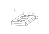
- FIG. 1 is a perspective view showing an example of the configuration of a multilayer substrate according to an embodiment.
- FIG. 2 is a cross-sectional view taken along line AA of FIG.
- FIG. 3 is an enlarged cross-sectional view showing the configuration of an interface between a first member and a second member according to the embodiment.
- FIG. 4 is an enlarged cross-sectional view showing the configuration of the inner wall of the first member according to the embodiment.
- FIG. 5 is a perspective view showing an example of the configuration of a connecting substrate according to the embodiment.
- FIG. 6 is a perspective view showing another example of the configuration of the laminated substrate according to the embodiment.
- FIG. 7 is a cross-sectional view showing an example of the configuration of a semiconductor device according to the embodiment.
- FIG. 8 is a cross-sectional view showing an example of the configuration of a laminated substrate according to another embodiment 1.
- FIG. 9 is a cross-sectional view showing an example of the configuration of a laminated substrate according to another embodiment 2.
- FIG. 10 is a cross-sectional view showing an example of the configuration of a laminated substrate according to another embodiment 3.
- FIG. 11 is a cross-sectional view showing an example of the configuration of a laminated substrate according to another embodiment 4.
- FIG. FIG. 12 is a cross-sectional view showing an example of the configuration of a laminated substrate according to another embodiment 5.
- FIG. 13 is a cross-sectional view showing an example of the configuration of a laminated substrate according to another embodiment 6.
- FIG. 14 is a cross-sectional view showing an example of the configuration of a laminated substrate according to another embodiment 7. As shown in FIG.
- substrates made of organic resin and molded into a frame shape have been used as substrates for semiconductor devices.
- the above-mentioned conventional technology has the problem that the substrate has low rigidity and is prone to bending. This can lead to a decrease in the reliability of the semiconductor device.
- Fig. 1 is a perspective view showing an example of the configuration of the laminated substrate 1 according to an embodiment
- Fig. 2 is a cross-sectional view taken along line AA in Fig. 1.
- the laminated substrate 1 has a first member 2 and a second member 3.
- the first member 2 is frame-shaped (rectangular frame-shaped) and made of organic resin.
- the second member 3 is frame-shaped (rectangular frame-shaped) and made of ceramic.
- the organic resin constituting the first member 2 is, for example, one selected from the group consisting of epoxy resin, polyimide resin, cyclic olefin resin, and polyphenylene ether resin.
- the ceramic constituting the second member 3 is, for example, one selected from the group consisting of alumina, alumina-zirconia composite, mullite, aluminum nitride, silicon nitride, and silicon carbide.
- alumina includes not only a single-component metal oxide of alumina (Al 2 O 3 ), but also so-called alumina ceramics in which a sintering aid is added to alumina.
- ceramics containing sintering aids are selected as suitable materials for alumina-zirconia composites, mullite, aluminum nitride, silicon nitride, and silicon carbide.
- the first member 2 and the second member 3 are laminated on top of each other.
- the inner frame portion 2a of the first member 2 and the inner frame portion 3a of the second member 3 are connected.
- the inner frame portion 1a including the inner frame portion 2a and the inner frame portion 3a is located inside the laminated substrate 1.
- the frame-shaped laminated substrate 1 is composed of a first member 2 made of organic resin and a second member 3 made of ceramic. This allows for improved rigidity compared to a frame-shaped substrate composed only of organic resin. Therefore, according to the embodiment, the bending strength of the frame-shaped substrate can be improved.
- the frame-shaped laminated substrate 1 is composed of a first member 2 made of organic resin and a second member 3 made of ceramic, so that, compared to a substrate composed only of organic resin, even if the substrate is made thinner, rigidity can be ensured without adding additional reinforcing members.
- the volume of the second member 3 can be reduced by the amount of the inner frame portion 3a. Therefore, according to the embodiment, the laminated substrate 1 can be made lighter.
- the inner wall 2b of the first member 2 and the inner wall 3b of the second member 3 may both be parallel to the stacking direction D. This makes it easier to control the direction of reflection when light emitted from the semiconductor element 21 is reflected by the inner wall 2b or the inner wall 3b, for example, when the semiconductor element 21 is a light-emitting element.
- the inner wall 2b of the first member 2 and the inner wall 3b of the second member 3 may be flush with each other. This allows the inner wall 2b and the inner wall 3b to form an integrated flat surface, so that, for example, when the semiconductor element 21 is a light-emitting element, it becomes easier to control the direction of reflection of light emitted from the semiconductor element 21.
- the inner frame portion 2a of the first member 2 and the inner frame portion 3a of the second member 3 being connected means that the space provided inside the first member 2 (first space) and the space provided inside the second member 3 (second space) form a single continuous space.
- the volume of the space (first space) provided inside the first member 2 is the same as the volume of the space (second space) provided inside the second member 3.
- FIG. 3 is an enlarged cross-sectional view showing the structure of the interface between the first member 2 and the second member 3 according to the embodiment.
- the first member 2 and the second member 3 may be bonded via carbon particles 4. That is, in the embodiment, the carbon particles 4 (boundary type carbon particles 4) may be positioned so as to be in contact with both the first bonding surface 2d of the first member 2 and the second bonding surface 3d of the second member 3.
- the carbon particles 4, which have a low specific gravity, may be sparsely positioned between the first member 2 and the second member 3.
- the organic resin component of the first member 2 may be directly bonded to the second bonding surface 3d of the second member 3.
- the carbon particles 4 may have a portion that penetrates into the first recess 2d1 located on the first bonding surface 2d of the first member 2 and the second recess 3d1 located on the second bonding surface 3d of the second member 3.
- the majority of the carbon particles 4 may penetrate into the first recess 2d1 and the second recess 3d1 at the interface between the first member 2 and the second member 3.
- the carbon particles 4 are restrained by the first member 2 and the second member 3, so that even if the entire laminated substrate 1 is deformed, the carbon particles 4 are less likely to fall off from the laminated substrate 1.
- the carbon particles 4 may penetrate more deeply into the first member 2 made of organic resin than into the second member 3 made of ceramic.
- the boundary-type carbon particles 4 located at the boundary between the first member 2 and the second member 3 have a first portion 4a that penetrates into the first recess 2d1 and a second portion 4b that penetrates into the second recess 3d1, and in the case of such boundary-type carbon particles 4, it is preferable that the first portion 4a located on the first member 2 side is larger than the second portion 4b located on the second member 3 side.
- the carbon particles 4 are more strongly constrained relative to the first member 2, so that even if the entire laminated substrate 1 is deformed, the carbon particles 4 are less likely to fall off from the first member 2.
- FIG. 4 is an enlarged cross-sectional view showing the configuration of the inner wall 2b of the first member 2 according to the embodiment.
- the first member 2 according to the embodiment contains a plurality of inorganic fillers F.
- the inorganic fillers F include the above-mentioned carbon particles 4 (see FIG. 3) and particles composed of an inorganic component different from the carbon particles 4 (e.g., silica, etc.).
- a resin layer 2b1 having less inorganic filler F than the inside of the first member 2 may be located on the surface of the inner wall 2b.
- the thickness of the resin layer 2b1 is, for example, 0.1 ⁇ m or more and 5 ⁇ m or less.
- “inside the first member 2" refers to a position deeper than 0.1 ⁇ m from the surface of the inner wall 2b.
- a resin layer 2b1 made of an organic resin component may be located on the inner wall 2b of the first member 2. And, in the embodiment, the surface of this resin layer 2b1 may have a glossy surface.
- the semiconductor element 21 when the semiconductor element 21 (see FIG. 7) is an imaging element, it is possible to reduce the diffuse reflection of light incident on the semiconductor element 21 by the inner wall 2b. Therefore, according to the embodiment, it is possible to obtain a high-resolution image.
- the inorganic filler F may be exposed from the outer edge 2c of the first member 2 (see FIG. 2).
- the outer edge 2c of the first member 2 does not need to have a resin layer formed therein that contains less inorganic filler F than the inside of the first member 2.
- FIG. 5 is a perspective view showing an example of the configuration of a connecting substrate 10 according to an embodiment.
- the connecting substrate 10 according to the embodiment is formed by connecting a plurality of the laminated substrates 1 described so far in a line along a plane perpendicular to the stacking direction D (see FIG. 2).
- the connecting substrate 10 has a plurality of laminated substrates 1 arranged in a matrix.
- the connecting substrate 10 may have a cutting line (not shown) between adjacent second members 3.
- a cutting line may be located, for example, on the surface of a ceramic member formed by connecting multiple second members 3.
- the connecting substrate 10 can be cut starting from the cutting line, making it easy to manufacture multiple laminated substrates 1.
- the cutting line may be located between adjacent first members 2, or may not be located. By locating the cutting line on the surface of the organic resin member formed by connecting multiple first members 2, multiple laminated substrates 1 can be manufactured more easily.
- this connecting substrate 10 has a configuration in which the first member 2 without a cutting line is laminated on the second member 3 with a cutting line.
- the location of the groove-shaped cut line may become a source of destruction for the connecting substrate 10, but since the first member 2 does not have a groove-shaped cut line, the first member 2 is attached to the second member 3, which prevents the connecting substrate 10 from cracking or chipping.
- a groove-shaped cutting line is provided between the first member 2 and the second member 3, it is possible to prevent dust and other particles from adhering to the groove from the stage of manufacturing the connecting substrate to the stage of cutting it to obtain the laminated substrate 1.
- the first member 2 is transparent (translucent)
- image recognition of the cutting line is possible, and therefore automatic cutting of the connecting substrate 10 based on image recognition is also possible.
- multiple laminated substrates 1 can be manufactured without any particular problems because the organic resin member is easily broken.
- FIG. 6 is a perspective view showing another example of the configuration of the laminated substrate 1 according to the embodiment.
- the example of FIG. 6 differs from the example of FIG. 1 in that a wiring layer 5 is located on the laminated substrate 1.
- This wiring layer 5 is located, for example, on the surface 2e of the first member 2.
- the wiring layer 5 may be electrically connected to via wiring, an internal wiring layer, etc. (not shown).
- FIG. 7 is a cross-sectional view showing an example of the configuration of a semiconductor device 20 according to an embodiment.
- the semiconductor device 20 according to an embodiment includes a multilayer substrate 1, a semiconductor element 21, a support plate 22, and a bonding wire 23.
- the multilayer substrate 1 shown in FIG. 7 includes the wiring layer 5 described above.
- the semiconductor element 21 is, for example, an LSI (Large Scale Integration), an imaging element, a light-emitting element, a quantum element, or an elastic wave element.
- the support plate 22 is, for example, a metal plate, and supports the semiconductor element 21.
- the support plate 22 is, for example, positioned so as to cover the bottom of the inner frame portion 1a, and the semiconductor element 21 is positioned at the bottom of the inner frame portion 1a.
- the bonding wires 23 electrically connect the wiring layer 5 located on the laminated substrate 1 to the semiconductor element 21.
- the member electrically connecting the wiring layer 5 to the semiconductor element 21 is not limited to the bonding wires 23, and may be, for example, a lead frame.
- the semiconductor device 20 has a semiconductor element 21 supported on a support plate 22 positioned to cover the bottom of the inner frame portion 1a, but the present disclosure is not limited to this example, and the semiconductor element 21 may be supported in any manner.
- Fig. 8 is a cross-sectional view showing an example of the configuration of a laminated substrate 1 according to another embodiment 1. As shown in Fig. 8, in the laminated substrate 1 according to another embodiment 1, the configuration of the inner wall 2b is different from that of the above-mentioned embodiment.
- a part of the inner wall 2b of the first member 2 may cover the inner wall 3b of the second member 3.
- the covering portion 2b2 may be located on the second member 3 side of the inner wall 2b of the first member 2, and the covering portion 2b2 may cover a part of the inner wall 3b of the second member 3 on the first member 2 side.
- the configuration shown in FIG. 8 can be formed, for example, by plastically deforming an uncured organic resin sheet that will later become the first member 2 when the uncured organic resin sheet is laminated and pressurized and heated on a ceramic second member 3 formed by sintering.
- the uncured organic resin sheet may be laminated in a state having an inner frame portion (a state having a through hole).
- FIG. 9 is a cross-sectional view showing an example of the configuration of the laminated substrate 1 according to another embodiment 2. As shown in FIG. 9, in the laminated substrate 1 according to another embodiment 2, the positions of the inner wall 2b and the inner wall 3b are different from those of the above embodiment.
- the area of the inner frame portion 2a of the first member 2 may be larger than the area of the inner frame portion 3a of the second member 3 in a plan view.
- the inner wall 2b of the first member 2 may be located outside the inner wall 3b of the second member 3.
- the volume ratio of the first member 2 to the entire laminated substrate 1 becomes smaller, so that the Young's modulus of the entire laminated substrate 1 depends heavily on the ceramic second member 3. Therefore, according to another embodiment 2, the rigidity per unit volume can be improved.
- FIG. 10 is a cross-sectional view showing an example of the configuration of the laminated substrate 1 according to another embodiment 3. As shown in FIG. 10, in the laminated substrate 1 according to another embodiment 3, the configuration of the first member 2 differs from that of the above-described another embodiment 2.
- a part of the first member 2 may be flared toward the step portion 3b1 (horizontal portion connected to the inner wall 3b) of the second member 3.
- the covering portion 2b3 may be located on the second member 3 side of the inner wall 2b of the first member 2, and the covering portion 2b3 may cover a part of the step portion 3b1 connected to the inner wall 3b of the second member 3.
- the configuration shown in FIG. 10 can be formed, for example, by plastically deforming an uncured organic resin sheet that will later become the first member 2 when the uncured organic resin sheet is laminated and pressurized and heated on a ceramic second member 3 formed by sintering.
- the uncured organic resin sheet may be laminated in a state having an inner frame portion (a state having a through hole).
- FIG. 11 is a cross-sectional view showing an example of the configuration of a laminated substrate 1 according to another embodiment 4. As shown in FIG. 11, in the laminated substrate 1 according to another embodiment 4, the positions of the outer edge portion 2c and the outer edge portion 3c are different from those of the above embodiment.
- the outer edge 2c of the first member 2 may be positioned outside the outer edge 3c of the second member 3 in a plan view.
- the laminated substrate 1 is less likely to crack even if the semiconductor device 20 (see FIG. 7) is subjected to a mechanical shock such as being dropped.
- the reliability of the semiconductor device 20 can be improved.
- FIG. 12 is a cross-sectional view showing an example of the configuration of a laminated substrate 1 according to another embodiment 5.
- the area of the inner frame portion 2a of the first member 2 may be larger than the area of the inner frame portion 3a of the second member 3 in a plan view.
- the semiconductor element 21 (see FIG. 7) is an image sensor, a wider range of light is captured by the semiconductor element 21. Therefore, according to the alternative embodiment 5, it is possible to obtain a high-resolution image.
- the outer edge 2c of the first member 2 may be located outside the outer edge 3c of the second member 3 in a plan view. This makes it difficult for the laminated substrate 1 to crack even if the semiconductor device 20 (see FIG. 7) is subjected to a mechanical shock such as being dropped.
- the reliability of the semiconductor device 20 can be improved.
- FIG. 13 is a cross-sectional view showing an example of the configuration of a laminated substrate 1 according to another embodiment 6. As shown in FIG. 13, in the laminated substrate 1 according to another embodiment 6, the orientation of the inner wall 2b is different from that of the above embodiment.
- the inner frame portion 2a of the first member 2 may become smaller as it approaches the second member 3. That is, in another embodiment 6, the inner wall 2b of the first member 2 may be inclined inward as it approaches the second member 3.
- the inner wall 2b of the first member 2 is inclined inward as it approaches the second member 3, but the present disclosure is not limited to such an example.
- the inner wall 2b of the first member 2 may be inclined outward as it approaches the second member 3.
- the center of the inner wall 2b of the first member 2 in the stacking direction D may be located outside both ends in the stacking direction D.
- the inner wall 2b of the first member 2 may be curved in a concave shape in cross-sectional view.
- the center of the inner wall 2b of the first member 2 in the stacking direction D may be located inside both ends in the stacking direction D.
- the inner wall 2b of the first member 2 may be curved in a convex shape in a cross-sectional view.
- FIG. 14 is a cross-sectional view showing an example of the configuration of a laminated substrate 1 according to another embodiment 7.
- the surface 2e of the first member 2 may be inclined so that the thickness of the first member 2 is greater on the inner wall 2b side than on the outer edge 2c side.
- the present technology can also be configured as follows.
- a frame-shaped second member made of ceramic; Equipped with The first member and the second member are stacked on each other, a laminated substrate, wherein an inner frame portion of the first member and an inner frame portion of the second member are connected to each other.
- the first member has a first bonding surface bonded to the second member and a first recess provided on the first bonding surface
- the second member has a second bonding surface bonded to the first bonding surface and a second recess provided on the second bonding surface
- the laminated substrate according to (4), wherein the plurality of carbon particles include boundary-existing carbon particles that enter the first recess and the second recess.
- the boundary-type carbon particle has a first portion that enters the first recess and a second portion that enters the second recess,
- the first member includes an inorganic filler,
- a plurality of laminated substrates according to any one of (1) to (8) are connected in a line along a plane perpendicular to the lamination direction, A cutting line is located between adjacent second members of the connecting substrate.
Landscapes
- Production Of Multi-Layered Print Wiring Board (AREA)
- Solid State Image Pick-Up Elements (AREA)
Priority Applications (2)
| Application Number | Priority Date | Filing Date | Title |
|---|---|---|---|
| JP2024565747A JPWO2024135312A1 (https=) | 2022-12-22 | 2023-12-04 | |
| CN202380086751.7A CN120380593A (zh) | 2022-12-22 | 2023-12-04 | 层叠基板、连接基板以及半导体装置 |
Applications Claiming Priority (2)
| Application Number | Priority Date | Filing Date | Title |
|---|---|---|---|
| JP2022206054 | 2022-12-22 | ||
| JP2022-206054 | 2022-12-22 |
Publications (1)
| Publication Number | Publication Date |
|---|---|
| WO2024135312A1 true WO2024135312A1 (ja) | 2024-06-27 |
Family
ID=91588286
Family Applications (1)
| Application Number | Title | Priority Date | Filing Date |
|---|---|---|---|
| PCT/JP2023/043238 Ceased WO2024135312A1 (ja) | 2022-12-22 | 2023-12-04 | 積層基板、連結基板および半導体装置 |
Country Status (3)
| Country | Link |
|---|---|
| JP (1) | JPWO2024135312A1 (https=) |
| CN (1) | CN120380593A (https=) |
| WO (1) | WO2024135312A1 (https=) |
Cited By (1)
| Publication number | Priority date | Publication date | Assignee | Title |
|---|---|---|---|---|
| WO2025116003A1 (ja) * | 2023-11-30 | 2025-06-05 | 京セラ株式会社 | 配線基板および半導体デバイス |
Citations (4)
| Publication number | Priority date | Publication date | Assignee | Title |
|---|---|---|---|---|
| WO2016042819A1 (ja) * | 2014-09-19 | 2016-03-24 | 京セラ株式会社 | 電子素子実装用基板および電子装置 |
| WO2017200011A1 (ja) * | 2016-05-20 | 2017-11-23 | 京セラ株式会社 | 電子素子実装用基板および電子装置 |
| WO2019168056A1 (ja) * | 2018-02-27 | 2019-09-06 | 京セラ株式会社 | 半導体パッケージ、半導体装置および半導体パッケージの製造方法 |
| WO2021039963A1 (ja) * | 2019-08-29 | 2021-03-04 | 京セラ株式会社 | 実装基板および電子装置 |
-
2023
- 2023-12-04 WO PCT/JP2023/043238 patent/WO2024135312A1/ja not_active Ceased
- 2023-12-04 JP JP2024565747A patent/JPWO2024135312A1/ja active Pending
- 2023-12-04 CN CN202380086751.7A patent/CN120380593A/zh active Pending
Patent Citations (4)
| Publication number | Priority date | Publication date | Assignee | Title |
|---|---|---|---|---|
| WO2016042819A1 (ja) * | 2014-09-19 | 2016-03-24 | 京セラ株式会社 | 電子素子実装用基板および電子装置 |
| WO2017200011A1 (ja) * | 2016-05-20 | 2017-11-23 | 京セラ株式会社 | 電子素子実装用基板および電子装置 |
| WO2019168056A1 (ja) * | 2018-02-27 | 2019-09-06 | 京セラ株式会社 | 半導体パッケージ、半導体装置および半導体パッケージの製造方法 |
| WO2021039963A1 (ja) * | 2019-08-29 | 2021-03-04 | 京セラ株式会社 | 実装基板および電子装置 |
Cited By (1)
| Publication number | Priority date | Publication date | Assignee | Title |
|---|---|---|---|---|
| WO2025116003A1 (ja) * | 2023-11-30 | 2025-06-05 | 京セラ株式会社 | 配線基板および半導体デバイス |
Also Published As
| Publication number | Publication date |
|---|---|
| CN120380593A (zh) | 2025-07-25 |
| JPWO2024135312A1 (https=) | 2024-06-27 |
Similar Documents
| Publication | Publication Date | Title |
|---|---|---|
| CN112020771B (zh) | 电子元件安装用基板、电子装置以及电子模块 | |
| TWI270184B (en) | Package for mounting an optical element and a method of manufacturing the same | |
| WO2024135312A1 (ja) | 積層基板、連結基板および半導体装置 | |
| CN101800201A (zh) | 电子元件用封装体和电子部件 | |
| CN118922935A (zh) | 布线基板及半导体装置 | |
| CN111418055A (zh) | 电子元件安装用基板、电子装置以及电子模块 | |
| JP6705861B2 (ja) | 電子装置 | |
| TW201924099A (zh) | 發光裝置 | |
| US20240251505A1 (en) | Electrical element- mounting substrate and electrical device | |
| JP7176103B2 (ja) | 電子素子実装用基板、および、電子装置 | |
| JP6208447B2 (ja) | 電子素子収納用パッケージおよび電子装置 | |
| CN110875258A (zh) | 电子元件安装用基板、电子装置以及电子模块 | |
| CN1362738A (zh) | 功率半导体模块 | |
| CN1701441A (zh) | 制造电子元件的方法 | |
| CN113875000A (zh) | 电子元件安装用基板、电子装置以及电子模块 | |
| CN108735706B (zh) | 电子元件安装用基板、电子装置以及电子模块 | |
| CN107004646A (zh) | 电子装置 | |
| CN114450860B (zh) | 光元件搭载用封装件、电子装置以及电子模块 | |
| CN114270499A (zh) | 安装基板以及电子装置 | |
| WO2025116005A1 (ja) | 配線基板および半導体デバイス | |
| TWI785195B (zh) | 半導體裝置 | |
| JP7825160B2 (ja) | 実装基板及び実装基板の製造方法 | |
| WO2025116016A1 (ja) | 配線基板および半導体デバイス | |
| WO2025116003A1 (ja) | 配線基板および半導体デバイス | |
| JP7227019B2 (ja) | 電子素子実装用基板、電子装置、および電子モジュール |
Legal Events
| Date | Code | Title | Description |
|---|---|---|---|
| 121 | Ep: the epo has been informed by wipo that ep was designated in this application |
Ref document number: 23906678 Country of ref document: EP Kind code of ref document: A1 |
|
| WWE | Wipo information: entry into national phase |
Ref document number: 202380086751.7 Country of ref document: CN |
|
| WWE | Wipo information: entry into national phase |
Ref document number: 2024565747 Country of ref document: JP |
|
| NENP | Non-entry into the national phase |
Ref country code: DE |
|
| WWP | Wipo information: published in national office |
Ref document number: 202380086751.7 Country of ref document: CN |
|
| 122 | Ep: pct application non-entry in european phase |
Ref document number: 23906678 Country of ref document: EP Kind code of ref document: A1 |