WO2024134713A1 - 直流遮断システム、直流遮断装置の制御方法、および直流遮断装置の制御プログラム - Google Patents
直流遮断システム、直流遮断装置の制御方法、および直流遮断装置の制御プログラム Download PDFInfo
- Publication number
- WO2024134713A1 WO2024134713A1 PCT/JP2022/046635 JP2022046635W WO2024134713A1 WO 2024134713 A1 WO2024134713 A1 WO 2024134713A1 JP 2022046635 W JP2022046635 W JP 2022046635W WO 2024134713 A1 WO2024134713 A1 WO 2024134713A1
- Authority
- WO
- WIPO (PCT)
- Prior art keywords
- circuit breaker
- circuit
- main circuit
- main
- current
- Prior art date
- Legal status (The legal status is an assumption and is not a legal conclusion. Google has not performed a legal analysis and makes no representation as to the accuracy of the status listed.)
- Ceased
Links
Images








Classifications
-
- H—ELECTRICITY
- H01—ELECTRIC ELEMENTS
- H01H—ELECTRIC SWITCHES; RELAYS; SELECTORS; EMERGENCY PROTECTIVE DEVICES
- H01H33/00—High-tension or heavy-current switches with arc-extinguishing or arc-preventing means
- H01H33/02—Details
- H01H33/59—Circuit arrangements not adapted to a particular application of the switch and not otherwise provided for, e.g. for ensuring operation of the switch at a predetermined point in the AC cycle
Definitions
- Embodiments of the present invention relate to a DC circuit breaker system, a control method for a DC circuit breaker, and a control program for a DC circuit breaker.
- DC circuit breakers including this will be simply referred to as "DC circuit breakers"
- Some DC circuit breakers are equipped with a main circuit breaker that performs fault breaking by cutting off the fault point when an accident occurs on a DC line, and a commutation circuit (also called a resonant circuit) that supplies a high-frequency current to cancel the current flowing through the main circuit breaker.
- This system is called a forced arc-extinguishing system.
- This type of DC circuit breaker includes one that performs high-speed reclosing, and conventional technologies for forced arc-extinguishing DC circuit breakers that perform fault breaking after high-speed reclosing include technologies that include multiple resonant circuits and technologies that include a bridge circuit as a resonant circuit.
- the object of the present invention is to provide a DC circuit breaking system that can be made compact in structure, a control method for a DC circuit breaking device, and a control program for a DC circuit breaking device.
- the DC interruption system is characterized by comprising a main circuit breaker provided on a DC line, a commutation circuit connected in parallel to the main circuit breaker and supplying a resonant current to the main circuit breaker when the main circuit breaker is opened, a rectification circuit connected in parallel to the commutation circuit and capable of maintaining a conductive state until the insulation performance of the main circuit breaker is restored when the main circuit breaker is opened, and a control device that controls the main circuit breaker, the commutation circuit, and the rectification circuit.
- FIG. 1 is a block diagram showing a configuration of a DC interruption system according to an embodiment; 1 is a block diagram showing a basic configuration of a DC interrupting device according to an embodiment; 1 is a block diagram showing a commutation circuit according to a first example of a DC interrupter according to an embodiment.
- FIG. FIG. 11 is a block diagram showing a commutation circuit according to a second example of the DC interrupter according to the embodiment.
- FIG. 11 is a block diagram showing a commutation circuit according to a third example of a direct current interrupting device according to an embodiment.
- FIG. 11 is a block diagram showing a commutation circuit according to a fourth example of a DC interrupter according to an embodiment.
- FIG. 1 is a block diagram showing an energy absorption circuit according to a first example of a DC interrupter according to an embodiment.
- FIG. FIG. 2 is a block diagram showing an energy absorption circuit according to a second example of a DC interrupting device according to an embodiment.
- FIG. 11 is a block diagram showing an energy absorption circuit according to a third example of a DC breaking device according to an embodiment.
- FIG. 11 is a block diagram showing an energy absorption circuit according to a fourth example of a DC interrupting device according to an embodiment.
- FIG. 10 is a block diagram showing an energy absorption circuit according to a fifth example of a DC interrupting device according to an embodiment.
- FIG. 13 is a block diagram showing an energy absorption circuit according to a sixth example of a DC breaking device according to an embodiment.
- FIG. 1 is a block diagram showing a rectifier circuit according to a first example of a direct current interrupting device according to an embodiment
- 4 is a block diagram showing a rectifier circuit according to a second example of the DC circuit breaking device according to the embodiment.
- FIG. FIG. 11 is a block diagram showing a rectifier circuit according to a third example of the DC circuit breaking device according to the embodiment.
- FIG. 11 is a block diagram showing a rectifier circuit according to a fourth example of the DC circuit breaking device according to the embodiment.
- FIG. 10 is a block diagram showing a rectifier circuit according to a fifth example of the DC circuit breaking device according to the embodiment.
- 4 is a flow chart showing a procedure for performing an interruption duty in a control method for a DC interruption device according to an embodiment.
- FIG. 1 is a graph showing an example of a time progression of a DC interruption system according to an embodiment. 4 is a flow chart showing a procedure of high-speed reclosing in the control method of the DC circuit breaker according to the embodiment.
- FIG. 1 is a first graph for explaining the effect of the DC interruption system according to the embodiment.
- 11 is a second graph for explaining the effect of the DC interruption system according to the embodiment.
- FIG. 1 is a block diagram showing a configuration of a DC interruption system 200 according to an embodiment.
- the DC interruption system 200 includes a DC interrupting device 100 and a control device 210.
- the DC circuit breaker 100 has a main circuit breaker 10, a commutation circuit 20, an energy absorption circuit 30, and a rectifier circuit 40.
- the main circuit breaker 10 is provided on a DC line 11.
- a power supply source such as a power plant
- a load is connected to the right side.
- the line 11a to which the power supply source is connected is referred to as the upstream side
- the load side line 11b to which the load is connected is referred to as the downstream side.
- the DC interruption system 200 described below can also be applied even if the left and right sides are reversed on the paper, with line 11a being the downstream side to which the load is connected, and line 11b being the upstream side to which the power supply source is connected.
- the main circuit breaker 10 may, for example, have a plurality of circuit breaker units, and the circuit breaker units may be configured as at least one of a vacuum circuit breaker, a gas circuit breaker, and a gap switch, or a combination of these.
- a saturable reactor may be connected in series to the main circuit breaker 10.
- the saturable reactor may be one or multiple saturable reactors connected in series.
- the main circuit breaker 10 may further include a voltage dividing circuit connected in parallel to the energy absorption circuit 30, which is an energy absorption unit.
- the voltage dividing circuit may be, for example, a circuit that operates to evenly or unevenly divide the inter-electrode voltage generated between the electrodes of the vacuum circuit breakers, gas circuit breakers, and gap switches in the multiple circuit breaking units.
- the circuit breaking unit may also include a circuit in which at least one of the vacuum circuit breakers, gas circuit breakers, and gap switches is connected in parallel to the energy absorption unit.
- the main circuit breaker 10 performs a circuit breaker operation, for example to isolate a faulty part of the system, in response to a command from the circuit breaker operating circuit 1.
- the commutation circuit 20 is provided to generate an AC component when the main circuit breaker 10 breaks the circuit. As shown in FIG. 1, the commutation circuit 20 is provided in parallel with the main circuit breaker 10. The commutation circuit 20 has a switch 21 and a capacitor 22 that are provided in series with each other.
- the energy absorption circuit 30 is an energy absorption unit provided to absorb residual energy stored in the DC system and the DC line when the main circuit breaker 10 cuts off the power.
- the energy absorption circuit 30 has metal oxide surge arresters (MOSA) 31 and a reactor 32, which are provided in parallel with the main circuit breaker 10.
- the reactor 32 is arranged in series with the commutation circuit 20.
- the lightning arrester 31 is composed of zinc oxide (ZnO) elements connected only in series, only in parallel, or a combination of series and parallel.
- the rectifier circuit 40 is provided in parallel with the main circuit breaker 10 and has a thyristor 41a and a thyristor 41b arranged in parallel in the opposite direction to each other.
- the control device 210 receives a shutoff command signal from the circuit breaker operating circuit 1 to the main circuit breaker 10, and outputs a specified command signal to the commutation circuit 20 and the rectification circuit 40.
- the control device 210 may cut off the location where the fault current occurred from the system, and then perform high-speed reclosing to quickly reconnect the system.
- the control device 210 when the system is reconnected by the rectifier circuit 40 after the main circuit breaker 10 cuts off the system, the control device 210 superimposes a current from the commutation circuit 20 on the fault current flowing through the rectifier circuit 40. If the fault does not continue after high-speed reclosing, the main circuit breaker 10 is closed again. If a charging circuit such as a pre-charging circuit for the capacitor 22 is provided, the control device 210 may be responsible for controlling the charging. Note that some DC interruption systems 200 do not perform high-speed reclosing. In this case, the control device 210 does not need to control high-speed reclosing after the main circuit breaker 10 cuts off the system.
- the control device 210 performs opening and closing control by, for example, a hardware processor such as a CPU (Central Processing Unit) executing a control program (software).
- the control device 210 may also perform opening and closing control by hardware (including circuitry) such as an LSI (Large Scale Integrator), ASIC (Application Specific Integrated Circuit), FPGA (Field-Programmable Gate Array), or GPU (Graphic Processing Unit), or may perform opening and closing control by collaboration between software and hardware.
- LSI Large Scale Integrator
- ASIC Application Specific Integrated Circuit
- FPGA Field-Programmable Gate Array
- GPU Graphic Processing Unit
- the control program may be stored in advance in a storage device (a storage device with a non-transient storage medium) such as the controller's HDD or flash memory, or may be stored in a removable storage medium such as a DVD or CD-ROM, and installed in the storage device by inserting the storage medium (non-transient storage medium) into a drive device.
- a storage device a storage device with a non-transient storage medium
- the control program may also be stored in other storage units.
- the current and voltage of each part are indicated by symbols as shown in Figure 1.
- the DC line current flowing through the DC line 11 is represented by I
- the main circuit breaker current flowing through the main circuit breaker 10 is represented by Ib
- the main circuit breaker voltage applied to the main circuit breaker 10 is represented by Vb
- the commutation circuit current flowing through the commutation circuit 20 is represented by It
- the switch voltage applied to the switch 21 of the commutation circuit 20 is represented by Vt.
- FIG. 2 is a block diagram showing the basic configuration of the DC circuit breaker 100 according to the embodiment.
- FIG. 2 is a basic configuration diagram for explaining the DC circuit breaker 100 according to the embodiment shown in FIG. 1, its components, and modified examples.
- the DC circuit breaker 100 has a main circuit breaker 10, an energy absorption circuit 30 and a rectifier circuit 40 that are respectively provided in parallel with the main circuit breaker 10, and a commutation circuit 20 that is electrically connected to the energy absorption circuit 30.
- the DC circuit breaker 100 according to this embodiment shown in Figure 1 is also based on this configuration.
- FIG. 3 is a block diagram showing a commutation circuit 20 according to a first example of the DC circuit breaker 100 according to the embodiment.
- the first example is the case of the commutation circuit 20 of the DC circuit breaker 100 according to the present embodiment shown in FIG. 1.
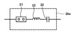
- FIG. 4 is a block diagram showing a commutation circuit 20a according to a second example of the DC circuit breaker 100 according to the embodiment.
- the commutation circuit 20a has a switch 21, a reactor 23, and a capacitor 22 arranged in series from the upstream side.
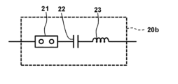
- FIG. 5 is a block diagram showing a commutation circuit 20b according to a third example of the DC circuit breaker 100 according to the embodiment.
- the commutation circuit 20b has a switch 21, a capacitor 22, and a reactor 23 arranged in series from the upstream side.
- FIG. 6 is a block diagram showing a commutation circuit 20c according to a fourth example of the DC circuit breaker 100 according to the embodiment.
- the commutation circuit 20c has a capacitor 22, a switch 21, and a reactor 23 arranged in series from the upstream side.
- any of the commutation circuits 20, 20a, 20b, and 20c may be combined to form a commutation circuit.
- Figs. 7 to 12 modified examples of the energy absorption circuit 30 will be described with reference to Figs. 7 to 12.
- the left side of the figure is the side connected to the power supply source line 11a (upstream side)
- the right side is the side connected to the load side line 11b (downstream side).
- the left and right sides of the paper may be reversed, and also the top and bottom of the paper may be reversed.
- FIG. 7 is a block diagram showing an energy absorption circuit 30 according to a first example of a DC circuit breaking device according to an embodiment.
- the first example is the energy absorption circuit 30 of the DC circuit breaking device 100 according to the present embodiment shown in FIG. 1.
- FIG. 8 is a block diagram showing an energy absorption circuit 30a according to a second example of a DC circuit breaker according to an embodiment.
- the energy absorption circuit 30a has a lightning arrester 31 arranged between the upstream side and the downstream side, and a reactor 32 arranged on the upstream side in the connection line with the commutation circuit 20 and on the downstream side in the connection line with the load side line 11b.
- FIG. 9 is a block diagram showing an energy absorption circuit 30b according to a third example of a DC circuit breaker according to an embodiment.
- the energy absorption circuit 30b has a lightning arrester 31 arranged between the upstream side and the downstream side, and reactors 32 arranged on the upstream side in the connection line with the commutation circuit 20 and on the upstream side in the connection line with the power supply source line 11a.
- FIG. 10 is a block diagram showing an energy absorption circuit 30c according to a fourth example of a DC circuit breaker according to an embodiment.
- the energy absorption circuit 30c has a lightning arrester 31 arranged between the upstream side and the downstream side, and reactors 32 arranged on the connection line to the power supply source line 11a and the connection line to the load side line 11b.
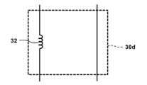
- FIG. 11 is a block diagram showing an energy absorption circuit 30d according to a fifth example of a DC circuit breaker according to an embodiment.
- the energy absorption circuit 30d has a reactor 32 arranged in a connection line with the power supply source side line 11a.
- the energy absorption circuit 30d does not include a lightning arrester 31.
- a connection line with the power supply source side line 11a connects the commutation circuit 20 and the rectification circuit 40 to the power supply source side line 11a
- a connection line with the load side line 11b connects the commutation circuit 20 and the rectification circuit 40 to the load side line 11b.
- FIG. 12 is a block diagram showing an energy absorption circuit 30e according to a sixth example of a DC circuit breaker according to an embodiment.
- the energy absorption circuit 30e has a lightning arrester 31 arranged between the upstream side and the downstream side. Note that the energy absorption circuit 30e does not have a reactor.
- any of the energy absorption circuits 30, 30a, 30b, 30c, 30d, and 30e may be combined to form an energy absorption circuit.
- FIG. 13 is a block diagram showing a rectifier circuit 40 according to a first example of a DC circuit breaker according to an embodiment.
- the first example is the rectifier circuit 40 of the DC circuit breaker 100 according to the present embodiment shown in FIG. 1.
- FIG. 14 is a block diagram showing a rectifier circuit 40a according to a second example of a DC circuit breaker according to an embodiment.
- the rectifier circuit 40a has a triode for alternating current (TRIAC) 42 arranged between the upstream side and the downstream side instead of the thyristors 41a and 41b in FIG. 1.
- TRIAC triode for alternating current
- FIG. 15 is a block diagram showing a rectifier circuit 40b according to a third example of a DC circuit breaker according to an embodiment.
- the rectifier circuit 40b has a diode 43 arranged in the forward direction from the downstream side to the upstream side, and a thyristor 41a arranged in parallel with the diode 43 and in the reverse direction to the diode 43.
- FIG. 16 is a block diagram showing a rectifier circuit 40c according to a fourth example of a DC circuit breaker according to an embodiment.
- the rectifier circuit 40c has a diode 43 arranged in the reverse direction from downstream to upstream, and a self-excited semiconductor 44 arranged in parallel with the diode 43.
- the self-excited semiconductor 44 may be an insulated gate bipolar transistor (IGBT), an injection enhanced gate transistor (IEGT), an integrated gate commutated turn-off thyristor (IGCT), or a gate turn-off thyristor (GTO).
- IGBT insulated gate bipolar transistor
- IEGT injection enhanced gate transistor
- IGCT integrated gate commutated turn-off thyristor
- GTO gate turn-off thyristor
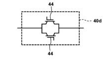
- FIG. 17 is a block diagram showing a rectifier circuit 40d according to a fifth example of a DC circuit breaker according to an embodiment.
- the rectifier circuit 40d has two self-excited semiconductors 44 arranged in parallel with each other and in opposite directions.
- the rectifier circuit may also be formed by combining any of the rectifier circuits 40, 40a, 40b, 40c, and 40d.
- the commutation circuit 20 and its variations, the energy absorption circuit 30 and its variations, and the rectifier circuit 40 and its variations according to this embodiment have been described above, but these can be combined in any way. Note that in the case of a combination of the commutation circuit 20 shown in FIG. 3 and the energy absorption circuit 30e shown in FIG. 12, no reactor is provided, but it is possible to generate an oscillation component by the L component (inductance) of the circuit.
- FIG. 18 is a flow diagram showing the procedure for performing the interruption duty in the control method of the DC circuit breaker 100 according to the embodiment.
- the area enclosed by solid lines shows the operation of the control device 210
- the area enclosed by dashed lines shows the transition of the state of the DC circuit breaker 100.
- FIG. 19 is a graph showing an example of the transition over time of the DC circuit breaker system according to the embodiment. The procedure for performing the interruption duty shown in FIG. 18 will be explained in sequence with reference to the graph in FIG. 19.
- the control device 210 sets the gate signals of the thyristors 41a and 41b of the rectifier circuit 40 to ON (step S11). That is, in preparation for the occurrence of an accident, the rectifier circuit 40 is in a state of conducting between the power supply source side line 11a and the load side line 11b in parallel with the main circuit breaker 10.
- the switch 21 of the commutation circuit 20 is open.
- the capacitor 22 is charged via, for example, a pre-charging circuit (not shown in FIG. 1) so as to generate a potential in the opposite direction to that of the DC line 11.
- the commutation circuit 20 is set to a charging state for the capacitor 22.
- an accident occurs (event transition W1).
- the control device 210 receives an accident occurrence signal (step S12).
- an accident refers to an accident occurring in the DC line 11 or a circuit or power system connected to it, resulting in a state in which the main circuit breaker 10 should be opened.
- the accident occurrence signal is caused by, for example, a ground fault, an overcurrent, a three-phase current, a voltage imbalance, etc., and is a direct or indirect output from these relays, or a command from another protection system.
- control device 210 When the control device 210 receives the accident occurrence signal, it outputs an open command to the main circuit breaker 10 (step S13). In response to the open command from the control device 210, the main circuit breaker 10 transitions to an open state at time t2 (FIG. 19). When the main circuit breaker 10 opens, an arc discharge occurs in the main circuit breaker 10, and the main circuit breaker 10 continues to be energized (event transition W2).
- the control device 210 After outputting the open command to the main circuit breaker 10, the control device 210 outputs a close command to the switch 21 of the commutation circuit 20 (step S14). At the same time as outputting the open command to the main circuit breaker 10, a close command may be output to the switch 21 of the commutation circuit 20. Also, before outputting the open command to the main circuit breaker 10, a close command may be output to the switch 21 of the commutation circuit 20. In response to the close command from the control device 210, the switch 21 of the commutation circuit 20 transitions to a closed state at time t3.
- the resonant current that flowed in the loop including the capacitor 22, the reactor 41, and the main circuit breaker 10 between time t3 and time t4 flows in the loop including the capacitor 22, the reactor 41, and the thyristors 41a and 41b that constitute the rectifier circuit 40 after time t4.
- the fault current Ib that flowed in the main circuit breaker 10 between time t1 and time t4 flows in the thyristors 41a and 41b that constitute the rectifier circuit 40 after time t4.
- both the fault current Ib and the resonant current flowing in the loop including the capacitor 22, the reactor 23, and the thyristors 41a and 41b that constitute the rectifier circuit 40 flow in the thyristors 41a and 41b that constitute the rectifier circuit 40 (event transition W4).
- step S15 the insulation performance of the main circuit breaker 10 returns to the recovered side (event transition W5).
- the control device 210 continues to check the insulation performance of the main circuit breaker 10 (step S15). In other words, if it is not determined that the insulation performance has recovered (step S16 NO), steps S15 and S16 are repeated.
- the insulation performance of the main circuit breaker 10 may be confirmed, for example, as a resistance value obtained by dividing the estimated voltage of the main circuit breaker 10 by the actual measurement of the current flowing through the main circuit breaker 10. Alternatively, it may be determined from the actual measurement of the voltage applied to both ends of the main circuit breaker and the estimated current. Alternatively, it may be determined from the actual measurement of the current flowing through the main circuit breaker 10 and the actual measurement of the voltage applied to both ends of the main circuit breaker.
- the voltage applied to both ends of the main circuit breaker 10 may be determined as the sum of the ON voltage of the thyristors and the product of the current change rate and the inductance component of the circuit.
- step S16 If it is determined that the insulation performance has been restored (step S16: YES), the control device 210 turns off the gate signals of the thyristors 41a and 41b of the rectifier circuit 40 (step S17).
- the rectifier circuit 40 maintains the conductive state until the current flowing through the thyristors 41a and 41b becomes zero. In FIG. 19, this corresponds to time t5.
- the fault current When the fault current is forcibly interrupted by such control, electromagnetic energy may remain in the system. This residual electromagnetic energy charges the capacitor 22 that constitutes the commutation circuit 20, and is disposed of by the energy absorption circuit 30.
- the fault current becomes current Ir and flows through the commutation circuit 20, which is made up of circuits excluding the main circuit breaker 10 and the rectifier circuit 40.
- the current Ir due to the fault current flowing through the commutation circuit 20 charges the capacitor 22 in the opposite direction to the direction in which it was previously charged while the switch 21 is "closed.” If we ignore the voltage induced in the reactor 32, the charging voltage Vc of the capacitor 22 is approximately equal to the voltage Vb across the main circuit breaker 10, and the lightning arrester 31, which is a unit of the energy absorption circuit 30, begins to process energy from the time when Vb rises to a certain voltage value.
- the control device 210 outputs an "open" command to the switch 21 again (step S18). Based on this, the switch 21 is opened again at time t7 in FIG. 19, and the capacitor 22 is isolated from the DC system. If a high-speed reclosing step is required, the switch 21 is opened again, so that the charging voltage Vc of the capacitor 22 can be maintained at a voltage value required for further accident processing.
- the voltage value may of course be increased or maintained by charging the capacitor 22 from a circuit not shown. Note that time t7 in FIG. 19 may precede event transition W6 where the DC interruption system 200 completes current interruption and thereby fulfills its interruption responsibility. In addition, if the switch 21 automatically performs an opening operation after a closing operation due to electromagnetic or mechanical repulsive force, the control device 210 does not need to output an "open" command to the switch 21.
- Figure 20 is a flow diagram showing the procedure of high-speed reclosing in the control method of the DC circuit breaker 100 according to the embodiment.
- control device 210 turns on the gate signal of the thyristor 41a of the rectifier circuit 40 (step S21, time t8 in FIG. 19). Furthermore, the control device 210 may turn on the gate signal of the thyristor 41b of the rectifier circuit 40.
- the control device 210 When the thyristor 41a constituting the rectifier circuit 40 is turned on to perform high-speed reclosing, if the fault does not continue, the control device 210 outputs a "close" command to the main circuit breaker 10 again (step S22). As a result, high-speed reclosing is achieved.
- a fault current flows through thyristor 41a, which constitutes the rectifier circuit.
- the direction of current Ib which is the fault current, becomes the same as the direction of the first fault current before high-speed reclosing is performed.
- the control device 210 detects that the accident continues and that current Ib is flowing again, and at time t9 turns off the gate signals of thyristors 41a and 41b. The conductive state is maintained until thyristors 41a and 41b are turned off.
- the switch 21 constituting the commutation circuit 20 is closed.
- a charge is discharged from the pre-charged capacitor 22 to a loop including the capacitor 22, the reactor 32, and the rectifier circuit 40.
- a resonant current flows from the capacitor 22 through the reactor 32 and the thyristor 41a.
- an oscillating current in the same direction as the fault current, current Ib is superimposed on the fault current, and then an oscillating current in the opposite direction is superimposed on the fault current due to resonance.
- the thyristor 41a is turned off at time t11. Thereafter, the electromagnetic energy remaining in the system is processed in the same manner as in the first fault interruption.
- the above is the processing flow when the thyristor 41a that constitutes the rectifier circuit 40 is turned ON to perform high-speed reclosing and the fault continues.
- the current Ib which is the fault current that flows through the main circuit breaker 10 due to an accident, flows in the opposite direction to the direction of the arrow in Figure 1.
- the switch 21 by closing the switch 21 at time t3 as the first fault interruption, an oscillating current in the same direction as the fault current Ib is superimposed on the fault current in the main circuit breaker 10, and then an oscillating current in the opposite direction to the current Ib is superimposed on the fault current due to resonance.
- the main circuit breaker 10 fulfills its interruption duty by completing the current interruption when a current zero point is formed at time t4.
- the fault current and oscillating current that were flowing through the main circuit breaker 10 flow through the thyristors 41a and 41b of the rectifier circuit 40.
- the thyristors 41a and 41b of the rectifier circuit 40 By turning off the gate signals of the thyristors 41a and 41b of the rectifier circuit 40 at time t5, the thyristors 41a and 41b are turned off at time t6 when the sum of the fault current and the oscillating current becomes zero, and the DC circuit breaker 100 completes fault interruption. After that, the electromagnetic energy remaining in the DC system is processed.
- the operation for cutting off the load current as the current to be cut off is the same as the first fault cutoff. That is, by opening the main circuit breaker 10 and closing the switch 21 of the commutation circuit 20, a resonant current flows as a result of the charge being released from the capacitor 22 to the loop including the capacitor 22, the switch 21, the reactor 32, and the main circuit breaker 10. As a result of the resonant current flowing, a current zero point is formed in the main circuit breaker 10, completing the current cutoff and fulfilling its cutting duty.
- the control device 210 of the DC circuit breaker 100 turns off the gate signals of the thyristors 41a and 41b of the rectifier circuit 40 at an appropriate time after the current zero point is formed in the main circuit breaker 10, so that the thyristors 41a and 41b are turned off at the time when the sum of the load current and the resonant current flowing through the thyristors 41a and 41b becomes zero.
- the rectifier circuit 40 becomes non-conductive and performs its interruption duty.
- the energy remaining in the system is processed by the energy absorption circuit 30.
- the DC circuit breaker 100 performs its current interruption duty.
- FIG. 21 is a first graph for explaining the effect of the DC interruption system according to the embodiment.
- FIG. 22 is a second graph for explaining the effect of the DC interruption system according to the embodiment.
- the first graph shows the response in the present embodiment
- the second graph shows the response in the conventional example shown as a comparative example.
- the horizontal axis in Figures 21 and 22 is time (msec)
- the vertical axis is the voltage value and current value in the main circuit breaker 10, both of which are relative values (pu).
- the time interval ⁇ t1 is approximately 100 times or more the time interval ⁇ t2, and the time interval ⁇ t1 is significantly larger than the time interval ⁇ t2.
- the value of the voltage change rate ( ⁇ Vcb/ ⁇ t), which is the slope connecting the point where the current value Ib of the main circuit breaker 10 becomes zero and the point where the absolute value of the voltage of the main circuit breaker 10 becomes maximum in the negative direction, is approximately 1/100th of the value in the case of FIG. 22 (comparative example) in the case of FIG. 21 (this embodiment), and is significantly smaller than the comparative example.
- the transient recovery voltage is applied immediately after the current flowing through the main circuit breaker becomes zero.
- the transient recovery voltage is applied a predetermined time after the current flowing through the main circuit breaker becomes zero.
- the voltage change rate ( ⁇ Vcb/ ⁇ t) which is the slope connecting the point where the current value Ib of the main circuit breaker 10 becomes zero and the point where the absolute value of the voltage of the main circuit breaker 10 becomes maximum in the negative direction, is significantly lower than in the conventional example. This makes it possible to reduce the risk of circuit breaker failure.
- the fault current and the oscillatory current are diverted to the rectifier circuit 40, so that the transient recovery voltage applied after the current zero point in the main circuit breaker 10 can be reduced. Therefore, the number of circuit breakers connected in series that make up the main circuit breaker 10 can be reduced, making it easier to reduce the size.
- the above-described embodiment makes it possible to provide a DC circuit breaking system that can be made compact in structure, a control method for a DC circuit breaking device, and a control program for a DC circuit breaking device.
- 1...circuit breaker operation circuit 10...main circuit breaker, 11...DC line, 11a...power supply source side line, 11b...load side line, 20, 20a, 20b, 20c...commutation circuit, 21...switch, 22...capacitor, 23...reactor, 30, 30a, 30b, 30c, 30d, 30e...energy absorption circuit, 31...lightning arrester, 32...reactor, 40, 40a, 40b, 40c, 40d...rectifier circuit, 41a, 41b...thyristor, 42...triac, 43...diode, 44...self-excited semiconductor, 100...DC circuit breaker, 200...DC circuit breaker system, 210...control device
Landscapes
- Engineering & Computer Science (AREA)
- Power Engineering (AREA)
- Driving Mechanisms And Operating Circuits Of Arc-Extinguishing High-Tension Switches (AREA)
Priority Applications (2)
| Application Number | Priority Date | Filing Date | Title |
|---|---|---|---|
| JP2024565398A JPWO2024134713A1 (https=) | 2022-12-19 | 2022-12-19 | |
| PCT/JP2022/046635 WO2024134713A1 (ja) | 2022-12-19 | 2022-12-19 | 直流遮断システム、直流遮断装置の制御方法、および直流遮断装置の制御プログラム |
Applications Claiming Priority (1)
| Application Number | Priority Date | Filing Date | Title |
|---|---|---|---|
| PCT/JP2022/046635 WO2024134713A1 (ja) | 2022-12-19 | 2022-12-19 | 直流遮断システム、直流遮断装置の制御方法、および直流遮断装置の制御プログラム |
Publications (1)
| Publication Number | Publication Date |
|---|---|
| WO2024134713A1 true WO2024134713A1 (ja) | 2024-06-27 |
Family
ID=91588044
Family Applications (1)
| Application Number | Title | Priority Date | Filing Date |
|---|---|---|---|
| PCT/JP2022/046635 Ceased WO2024134713A1 (ja) | 2022-12-19 | 2022-12-19 | 直流遮断システム、直流遮断装置の制御方法、および直流遮断装置の制御プログラム |
Country Status (2)
| Country | Link |
|---|---|
| JP (1) | JPWO2024134713A1 (https=) |
| WO (1) | WO2024134713A1 (https=) |
Citations (2)
| Publication number | Priority date | Publication date | Assignee | Title |
|---|---|---|---|---|
| JPS627738U (https=) * | 1985-06-29 | 1987-01-17 | ||
| WO2015087558A1 (ja) * | 2013-12-11 | 2015-06-18 | 三菱電機株式会社 | 直流遮断装置 |
Family Cites Families (2)
| Publication number | Priority date | Publication date | Assignee | Title |
|---|---|---|---|---|
| JPS5878334A (ja) * | 1981-11-02 | 1983-05-11 | 株式会社東芝 | 直流開閉器 |
| KR100344056B1 (ko) * | 1999-03-17 | 2002-07-22 | 주식회사 포스콘 | 직류 대전류 차단장치 |
-
2022
- 2022-12-19 JP JP2024565398A patent/JPWO2024134713A1/ja active Pending
- 2022-12-19 WO PCT/JP2022/046635 patent/WO2024134713A1/ja not_active Ceased
Patent Citations (2)
| Publication number | Priority date | Publication date | Assignee | Title |
|---|---|---|---|---|
| JPS627738U (https=) * | 1985-06-29 | 1987-01-17 | ||
| WO2015087558A1 (ja) * | 2013-12-11 | 2015-06-18 | 三菱電機株式会社 | 直流遮断装置 |
Also Published As
| Publication number | Publication date |
|---|---|
| JPWO2024134713A1 (https=) | 2024-06-27 |
Similar Documents
| Publication | Publication Date | Title |
|---|---|---|
| EP2777059B1 (en) | Hybrid dc circuit breaking device | |
| KR101522412B1 (ko) | 양방향 직류 차단장치 | |
| JP5622978B1 (ja) | 直流送電系統の保護システムおよび交流直流変換器ならびに直流送電系統の遮断方法 | |
| US9948089B2 (en) | DC circuit breaker device | |
| US10910817B2 (en) | DC circuit breaker | |
| JP6042035B2 (ja) | 直流遮断装置 | |
| EP3242309B1 (en) | High voltage dc circuit breaker | |
| CN110808572A (zh) | 开关装置 | |
| KR101766229B1 (ko) | 갭 스위치를 이용한 고압 직류 차단 장치 및 방법 | |
| WO2013164875A1 (ja) | 直流遮断器 | |
| CN109950866B (zh) | 电流切断器 | |
| JPWO2014038008A1 (ja) | 直流遮断器 | |
| JP6456575B1 (ja) | 直流遮断器 | |
| KR101522413B1 (ko) | 고전압 dc 차단기 | |
| CN114128067B (zh) | 直流配电盘 | |
| JP6424976B1 (ja) | 直流遮断装置 | |
| WO2024134713A1 (ja) | 直流遮断システム、直流遮断装置の制御方法、および直流遮断装置の制御プログラム | |
| JP7134375B1 (ja) | 直流遮断器 | |
| US11049677B2 (en) | Inverse current injection-type direct current blocking device and method using vacuum gap switch | |
| EP4560677A1 (en) | Circuit breaker | |
| JP7600430B2 (ja) | 直流遮断装置、直流遮断装置の制御装置、直流遮断装置の制御方法、及びプログラム | |
| JP7830672B2 (ja) | 直流電流遮断装置 | |
| WO2018198552A1 (ja) | 直流遮断装置 | |
| JP2025087155A (ja) | スイッチギヤ | |
| JP2002093291A (ja) | 半導体開閉器およびその制御方法 |
Legal Events
| Date | Code | Title | Description |
|---|---|---|---|
| 121 | Ep: the epo has been informed by wipo that ep was designated in this application |
Ref document number: 22968745 Country of ref document: EP Kind code of ref document: A1 |
|
| WWE | Wipo information: entry into national phase |
Ref document number: 2024565398 Country of ref document: JP |
|
| NENP | Non-entry into the national phase |
Ref country code: DE |
|
| 122 | Ep: pct application non-entry in european phase |
Ref document number: 22968745 Country of ref document: EP Kind code of ref document: A1 |