EP2777059B1 - Hybrid dc circuit breaking device - Google Patents
Hybrid dc circuit breaking device Download PDFInfo
- Publication number
- EP2777059B1 EP2777059B1 EP12813371.7A EP12813371A EP2777059B1 EP 2777059 B1 EP2777059 B1 EP 2777059B1 EP 12813371 A EP12813371 A EP 12813371A EP 2777059 B1 EP2777059 B1 EP 2777059B1
- Authority
- EP
- European Patent Office
- Prior art keywords
- circuit
- current path
- breaker
- switch
- parallel
- Prior art date
- Legal status (The legal status is an assumption and is not a legal conclusion. Google has not performed a legal analysis and makes no representation as to the accuracy of the status listed.)
- Active
Links
Images


Classifications
-
- H—ELECTRICITY
- H02—GENERATION; CONVERSION OR DISTRIBUTION OF ELECTRIC POWER
- H02H—EMERGENCY PROTECTIVE CIRCUIT ARRANGEMENTS
- H02H3/00—Emergency protective circuit arrangements for automatic disconnection directly responsive to an undesired change from normal electric working condition with or without subsequent reconnection ; integrated protection
- H02H3/08—Emergency protective circuit arrangements for automatic disconnection directly responsive to an undesired change from normal electric working condition with or without subsequent reconnection ; integrated protection responsive to excess current
-
- H—ELECTRICITY
- H01—ELECTRIC ELEMENTS
- H01H—ELECTRIC SWITCHES; RELAYS; SELECTORS; EMERGENCY PROTECTIVE DEVICES
- H01H9/00—Details of switching devices, not covered by groups H01H1/00 - H01H7/00
- H01H9/54—Circuit arrangements not adapted to a particular application of the switching device and for which no provision exists elsewhere
- H01H9/548—Electromechanical and static switch connected in series
-
- H—ELECTRICITY
- H01—ELECTRIC ELEMENTS
- H01H—ELECTRIC SWITCHES; RELAYS; SELECTORS; EMERGENCY PROTECTIVE DEVICES
- H01H33/00—High-tension or heavy-current switches with arc-extinguishing or arc-preventing means
- H01H33/02—Details
- H01H33/59—Circuit arrangements not adapted to a particular application of the switch and not otherwise provided for, e.g. for ensuring operation of the switch at a predetermined point in the AC cycle
- H01H33/596—Circuit arrangements not adapted to a particular application of the switch and not otherwise provided for, e.g. for ensuring operation of the switch at a predetermined point in the AC cycle for interrupting DC
-
- H—ELECTRICITY
- H02—GENERATION; CONVERSION OR DISTRIBUTION OF ELECTRIC POWER
- H02H—EMERGENCY PROTECTIVE CIRCUIT ARRANGEMENTS
- H02H1/00—Details of emergency protective circuit arrangements
- H02H1/0007—Details of emergency protective circuit arrangements concerning the detecting means
-
- H—ELECTRICITY
- H02—GENERATION; CONVERSION OR DISTRIBUTION OF ELECTRIC POWER
- H02H—EMERGENCY PROTECTIVE CIRCUIT ARRANGEMENTS
- H02H3/00—Emergency protective circuit arrangements for automatic disconnection directly responsive to an undesired change from normal electric working condition with or without subsequent reconnection ; integrated protection
- H02H3/08—Emergency protective circuit arrangements for automatic disconnection directly responsive to an undesired change from normal electric working condition with or without subsequent reconnection ; integrated protection responsive to excess current
- H02H3/087—Emergency protective circuit arrangements for automatic disconnection directly responsive to an undesired change from normal electric working condition with or without subsequent reconnection ; integrated protection responsive to excess current for DC applications
Definitions
- the present invention relates to a hybrid type dc circuit breaking device comprising a breaker circuit having serially connected mechanical and electronic switches and a capacitor in parallel with the serially connected switches; and more particularly the present invention relates to possible use of the breaker circuit in combination with one or more varistors to stop or allow the flow of dc current in an electric circuit. Moreover, this invention comprises the fast discharge circuit to allow for fast reclose of the dc breaker.
- Hybrid dc Circuit breaker as shown in Figure 1 is described in the publication " Protective Hybrid HVdc Breakers - A Key Innovation for Reliable HVdc Grids," by Jurgen Hafner and Bjorn Jacobson in CIGRE International Symposium, Bologna, Italy, Sept. 13-15, 2011 , which is incorporated herein by reference. More particularly in the publication a hybrid dc breaker is disclosed consisting of a mechanical fast disconnector, an electronic auxiliary dc breaker and an electronic main dc breaker as shown in Figure 1 . During the normal operation the fast disconnector, the auxiliary dc breaker and the residual dc current breaker are closed and the main dc breaker is open.
- the dc current flows through the residual dc current breaker, fast disconnector and the auxiliary dc breaker and current through the main dc breaker remains at almost zero.
- the auxiliary dc breaker is ordered to open and the main dc breaker is ordered to close. This will commutate the current to the main dc breaker in a very short time, normally a fraction of a millisecond.
- the mechanical fast disconnector is ordered to open. The mechanical fast disconnector opens at zero current as the dc current is already commutated to the main dc breaker. Once the mechanical fast disconnector is in open position the main dc breaker breaks the current.
- the hybrid dc breaker is able to break fault currents in a short time and has low losses when it is closed.
- the hybrid dc breaker described above offers an acceptable breaking time for most applications and reasonably low losses, however it requires an electronic main dc breaker.
- the main dc breaker must have a voltage rating higher than the rated voltage of the dc circuit. It may also be required that the main dc breaker be able to break the dc current in either direction, which will add to the complexity of its design and increase the number of its components.
- Document WO 2011/141428 A1 discloses such a circuit breaking device comprising a primary and a secondary current paths, an electronic breaker switch connected in series with a mechanical interrupter switch in the primary current path and a capacitor in the secondary current path.
- the present invention is similar to the above mentioned hybrid dc breaker in using a mechanical switch (which can be a fast disconnector) and an auxiliary electronic dc breaker, but it replaces the main dc breaker with a capacitor.
- a controller arranged to displace the mechanical switch into the open position immediately subsequent to opening of the electronic breaker switch.
- the electronic breaker switch can be opened shortly after opening the mechanical switch.
- the device also includes a tertiary current path connected in parallel with the primary current path and the secondary current path, and a varistor connected in the tertiary current path so as to be in parallel with the serially connected switches and in parallel with the capacitor.
- the device may further comprise an auxiliary current path connected in parallel with the first dc circuit in which the auxiliary current path includes an auxiliary varistor connected in series therewith.
- the device may further include a second auxiliary current path in parallel with the second dc circuit and a third varistor connected in the second auxiliary current path so as to be in parallel with the second dc circuit.
- the device may further comprise an auxiliary interrupter switch connected in series between the breaker circuit and either one of the first and second dc circuits.
- the device may further include a fourth current path connected in parallel to the primary and secondary current paths.
- the fourth current path preferably comprises a series connected switch and a damping circuit.
- the damping circuit may comprise a damping resistor and a damping inductor in which the resistor and the inductor are connected in parallel to each other and together in series with the switch.
- the damping circuit may comprise a damping resistor connected in series with a spark gap and a damping inductor connected in parallel to the serially connected damping resistor and spark gap.
- the switch can be mechanical, electronic, spark gap, plasma injection, vacuum tube or any other device or combination of devices that is capable of closing the circuit upon receiving a command signal and opening the circuit either by a command signal or when its current or voltage is reduced below a threshold level.
- the electronic breaker switch may comprise a solid state semiconductor based circuit breaker or a vacuum tube circuit breaker capable of interrupting current either in only one direction or in both directions.
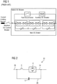
- a circuit breaking device generally indicated by reference numeral 20.
- the device 20 is particularly suited for use in series with the main current path 26 between a first direct current (dc) circuit 36 and a second (dc) circuit 7 in which the first and second dc circuits 36 and 7 generally include and any bus bars, overhead transmission lines, cables, reactors, breakers, converters or any other components which may be related.
- dc direct current
- dc direct current
- dc circuit 7 generally include and any bus bars, overhead transmission lines, cables, reactors, breakers, converters or any other components which may be related.
- the dc circuit 36 is assumed to consist of the ideal dc voltage source 1 and the inductor 2, however in general the dc circuit 36 can consist of any other components as mentioned.
- the device 20 generally includes a breaker circuit 22 represented in Figure 2 .
- the circuit 22 includes a primary current path 24 which is arranged to be connected to the main current path 26 connecting the first dc circuit 36 and the second dc circuit 7.
- the breaker circuit 22 also includes a secondary current path 28 which is connected in parallel with the primary current path such that the primary and secondary current paths are together parallel connected and collectively form the breaker circuit in series with the main current path between the first dc circuit 36 and the second dc circuit 7.
- a mechanical interrupter switch 3 is connected in the primary current path 24 in series therewith. Contacts of the mechanical interrupter switch are arranged to be moveable relative to one another between a closed position arranged to conduct current therethrough flowing through the primary current path, and an open position in which the primary current path is opened such that the current flowing therethrough is broken.
- An electronic breaker switch 4 is also connected in series with the mechanical interrupter switch 3 in the primary current path 24.
- the electronic breaker switch 4 is a solid state semi-conductor type breaker which is readily operable from a closed state to an open state upon receipt of an electronic opening signal from a suitable controller 18. In the closed state, the electronic breaker switch is arranged to conduct current flowing through the primary current path. In the open state the switch is arranged to break current flowing therethrough. A rated voltage of the electronic breaker switch is lower than the rated voltage of the dc circuits 7 and 36.
- the breaker circuit 22 further includes a capacitor 5 connected in the secondary current path 28 so as to be in parallel with the serially connected mechanical interrupter switch 3 and electronic breaker switch 4.
- the controller 18 of the electronic breaker switch is also arranged to order the interrupter switch 3 to be mechanically displaced from the closed position into the open position immediately subsequent to opening of the electronic breaker switch by sending the electronic opening signal to this switch.
- the device 20 further includes a tertiary current path 30 which is connected in parallel with the primary current path 24 and the secondary current path 28 and also forms part of the collective breaker circuit 22 connected in series with the main current path 26.
- a first varistor 6 is connected in the tertiary current path so as to be parallel with the serially connected switches 3 and 4 and in parallel with the capacitor 5.
- the device 20 also includes an auxiliary current path 32.
- the auxiliary current path 32 is connected in parallel with the dc circuit 36.
- a second varistor 8 can then be connected in series with the auxiliary current path 32 so as to be connected in parallel with the main current path serially connecting the breaker circuit 22 and the dc circuit 7.
- the device 20 includes all of the features of the previous embodiment together with an additional auxiliary current path 34 connected in parallel with the dc circuit 7.
- the auxiliary current path 34 and parallel connected dc current 7 are collectively connected in series with the breaker circuit 22.
- a third varistor 9 is connected in series with the auxiliary current path 34 such that the third varistor is in parallel with the second dc circuit 7 and the collective parallel connection of the third varistor and the second dc circuit 7 is in series between the breaker circuit 22 and the return path of the second dc circuit 7 to the first dc circuit 36.
- the device 20 includes all of the features of the previous embodiment along with an additional auxiliary interrupter switch 10 connected in series with the main current path between the first dc circuit 36 and the breaker circuit 22.
- the auxiliary interrupter switch 10 may be connected in series with the main current path 26 on the opposite side of the breaker circuit 22 between the breaker circuit 22 and the second dc circuit 7.
- the auxiliary current path 32 connects in parallel with the main current path between the dc circuit 36 and the auxiliary interrupter switch 10.
- the device 20 includes all of the features of the previous embodiments with an additional fourth current path 41 defining a supplementary current path connected in parallel to the primary current path 24 and the secondary current path 28 and the tertiary current path 30 so that they are collectively in series with the main current path 26.
- a damping resistor 39 and a damping inductor 40 are connected in parallel to each other and collectively define a damping circuit which is connected in series to the fourth current path 41.
- a switch 37 is connected in series with the fourth current path 41 and the damping circuit formed by the parallel combination of the damping resistor 39 and the damping inductor 40.
- the switch 37 can be mechanical, electronic, spark gap, plasma injection, vacuum tube or any other device or combination of devices that is capable of closing the circuit upon receiving a command signal and opening the circuit either by a command signal or when its current or voltage is reduced below a threshold level.
- the damping circuit may consist of a damping resistor 39 connected in series with a spark gap and a damping inductor 40 connected in parallel to the series combination of the damping resistor and the spark gap.
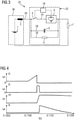
- Figure 3 shows an electric circuit consisting of a first dc circuit 36, a mechanical interrupter switch 3, an electronic breaker switch 4, a capacitor 5, a varistor 6 and the remaining parts of the dc circuit schematically shown as block 7.
- the first dc circuit 36 consists of a source of dc current 1 and an inductor 2 that represents the inductance present in the circuit, however in general the first dc circuit 36 can consist of any busbars, overhead transmission lines, cables, reactors, breakers, converters or any other components.
- the source 1 can be a battery, a dc generator or any kind of electronic ac to dc converter.
- the reactor 2 represents the total inductance present between the source and the breaker. This includes any physical inductor and the inductance of the busbars, conductors and any stray inductances.
- the mechanical switch 3 can be a circuit breaker, a load switch or a fast disconnector. This mechanical switch will open at near zero dc voltage and current.
- the electronic breaker 4 is an electronic switch made of IGBT's, GTO's, GeT's, electron tubes or any other electronic components that is capable of being turned on and off by an electronic signal.
- the voltage rating of the auxiliary breaker 4 is lower than the rated voltage of the dc circuit. If the hybrid dc circuit breaker is required to break the dc current in both directions, the auxiliary electronic breaker must be capable of blocking current in both directions.
- the remaining parts of the dc circuit including any busbars, overhead transmission lines, cables, reactors, breakers, converters or any other components are schematically shown as block 7.
- FIG. 5 shows a variation of the hybrid dc circuit breaker where a varistor 8 is added to the circuit.
- the knee voltage for varistor 8 is selected below the knee voltage for the varistor 6.
- Figure 6 shows the simulation results for a short circuit event similar to the case shown in Figure 4 .
- the new trace L8 represents the current through the varistor 8.
- Figure 6 shows that the current through the varistor 6 is reduced to almost zero in this arrangement.
- the hybrid dc breaker can be designed to break the current in both directions as explained earlier.
- the behaviour of the hybrid dc breaker is similar to the previous cases discussed above.
- the rate of rise for the fault current will depend on the inductance of the complete fault current path in this case. Similar to the previous example the flow of current through the varistor 6 may not be acceptable in some applications.
- a variation of the hybrid dc breaker shown in Figure 7 will reduce the current flow through varistor 6 to almost zero following a fault on either side of the breaker.
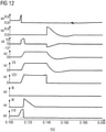
- FIG. 11 shows a fast discharge of the capacitor 5 and reclosing of the mechanical interrupter switch 3 and electronic breaker switch 4.
- Figure 12 shows a computer simulation example of the open and reclose procedure for the hybrid dc circuit breaker.
- the process of opening the dc breaker is similar to the process described in connection to the forth embodiment and the simulation example shown in Figure 10 .
- the capacitor 5 is charged to the voltage V_5 as shown in Figure 12 .
- the switch 37 is ordered to close. This will provide a path for capacitor 5 to discharge through the damping resistor 39 and the damping inductor 40.
- the resistance and inductance of these elements are selected such that the capacitor 5 is discharged within the required time.
- the mechanical interrupter switch 3 and electronic breaker switch 4 are ordered to close and the current flow through the breaker is resumed.
Landscapes
- Engineering & Computer Science (AREA)
- Power Engineering (AREA)
- Driving Mechanisms And Operating Circuits Of Arc-Extinguishing High-Tension Switches (AREA)
Description
- The present invention relates to a hybrid type dc circuit breaking device comprising a breaker circuit having serially connected mechanical and electronic switches and a capacitor in parallel with the serially connected switches; and more particularly the present invention relates to possible use of the breaker circuit in combination with one or more varistors to stop or allow the flow of dc current in an electric circuit. Moreover, this invention comprises the fast discharge circuit to allow for fast reclose of the dc breaker.
- A prior art Hybrid dc Circuit breaker as shown in
Figure 1 is described in the publication "Protective Hybrid HVdc Breakers - A Key Innovation for Reliable HVdc Grids," by Jurgen Hafner and Bjorn Jacobson in CIGRE International Symposium, Bologna, Italy, Sept. 13-15, 2011, which is incorporated herein by reference. More particularly in the publication a hybrid dc breaker is disclosed consisting of a mechanical fast disconnector, an electronic auxiliary dc breaker and an electronic main dc breaker as shown inFigure 1 . During the normal operation the fast disconnector, the auxiliary dc breaker and the residual dc current breaker are closed and the main dc breaker is open. The dc current flows through the residual dc current breaker, fast disconnector and the auxiliary dc breaker and current through the main dc breaker remains at almost zero. When the breaker is required to open the auxiliary dc breaker is ordered to open and the main dc breaker is ordered to close. This will commutate the current to the main dc breaker in a very short time, normally a fraction of a millisecond. At the same time the mechanical fast disconnector is ordered to open. The mechanical fast disconnector opens at zero current as the dc current is already commutated to the main dc breaker. Once the mechanical fast disconnector is in open position the main dc breaker breaks the current. The hybrid dc breaker is able to break fault currents in a short time and has low losses when it is closed. The hybrid dc breaker described above offers an acceptable breaking time for most applications and reasonably low losses, however it requires an electronic main dc breaker. The main dc breaker must have a voltage rating higher than the rated voltage of the dc circuit. It may also be required that the main dc breaker be able to break the dc current in either direction, which will add to the complexity of its design and increase the number of its components. DocumentWO 2011/141428 A1 discloses such a circuit breaking device comprising a primary and a secondary current paths, an electronic breaker switch connected in series with a mechanical interrupter switch in the primary current path and a capacitor in the secondary curent path. - The present invention is similar to the above mentioned hybrid dc breaker in using a mechanical switch (which can be a fast disconnector) and an auxiliary electronic dc breaker, but it replaces the main dc breaker with a capacitor.
- According to one aspect of the invention there is provided an arrangement according to claim 1.
- Preferably a controller arranged to displace the mechanical switch into the open position immediately subsequent to opening of the electronic breaker switch. Alternatively the electronic breaker switch can be opened shortly after opening the mechanical switch.
- In preferred embodiments the device also includes a tertiary current path connected in parallel with the primary current path and the secondary current path, and a varistor connected in the tertiary current path so as to be in parallel with the serially connected switches and in parallel with the capacitor.
- When the primary current path and the secondary current path define a breaker circuit in series with the main current path, the device may further comprise an auxiliary current path connected in parallel with the first dc circuit in which the auxiliary current path includes an auxiliary varistor connected in series therewith.
- The device may further include a second auxiliary current path in parallel with the second dc circuit and a third varistor connected in the second auxiliary current path so as to be in parallel with the second dc circuit.
- The device may further comprise an auxiliary interrupter switch connected in series between the breaker circuit and either one of the first and second dc circuits.
- The device may further include a fourth current path connected in parallel to the primary and secondary current paths.
- The fourth current path preferably comprises a series connected switch and a damping circuit. The damping circuit may comprise a damping resistor and a damping inductor in which the resistor and the inductor are connected in parallel to each other and together in series with the switch.
- Alternatively the damping circuit may comprise a damping resistor connected in series with a spark gap and a damping inductor connected in parallel to the serially connected damping resistor and spark gap.
- The switch can be mechanical, electronic, spark gap, plasma injection, vacuum tube or any other device or combination of devices that is capable of closing the circuit upon receiving a command signal and opening the circuit either by a command signal or when its current or voltage is reduced below a threshold level.
- The electronic breaker switch may comprise a solid state semiconductor based circuit breaker or a vacuum tube circuit breaker capable of interrupting current either in only one direction or in both directions. Various embodiments of the invention will now be described in conjunction with the accompanying drawings in which:
-
-
Figure 1 is a schematic representation of a prior art dc circuit breaking device including a hybrid of mechanical and electrical breakers. -
Figure 2 is a schematic representation of a dc circuit breaking device including a hybrid of mechanical and electrical breakers. -
Figure 3 is a schematic representation of the dc circuit breaking device ofFigure 2 with an additional tertiary current path and varistor in connection with two dc circuits. -
Figure 4 is a graphical representation of the dissipation of current and voltage in response to opening of the dc circuit breaking device inFigure 3 . -
Figure 5 is a schematic representation of the dc circuit breaking device ofFigure 3 in connection with two dc circuits with an additional auxiliary current path and an auxiliary varistor. -
Figure 6 is a graphical representation of the dissipation of current and voltage in response to opening of the dc circuit breaking device inFigure 5 . -
Figure 7 is a schematic representation of the dc circuit breaking device ofFigure 3 in connection with two dc circuits with two additional auxiliary current paths and auxiliary varistors. -
Figure 8 is a graphical representation of the dissipation of current and voltage in response to opening of the dc circuit breaking device inFigure 7 . -
Figure 9 is a schematic representation of the dc circuit breaking device ofFigure 3 in connection with two dc circuits with additional auxiliary current paths and varistors and an additional auxiliary interrupter switch. -
Figure 10 is a graphical representation of the dissipation of current and voltage in response to opening of the dc circuit breaking device inFigure 9 . -
Figure 11 is a schematic representation of the dc circuit breaking device ofFigure 9 in connection with two dc circuits with additional fourth current path comprising a switch and damping circuit consisting of a resistor and an inductor. -
Figure 12 is a graphical representation of the dissipation of current and voltage in response to opening of the dc circuit breaking device inFigure 11 and the reclose process which consists of discharging thecapacitor 5 byclosing switch 37 and then closing themechanical switch 3 and theelectronic switch 4 when the voltage acrosscapacitor 5 is sufficiently low. - In the drawings like characters of reference indicate corresponding parts in the different figures.
- Referring to the accompanying figures, there is illustrated a circuit breaking device generally indicated by
reference numeral 20. Thedevice 20 is particularly suited for use in series with the maincurrent path 26 between a first direct current (dc)circuit 36 and a second (dc) circuit 7 in which the first andsecond dc circuits 36 and 7 generally include and any bus bars, overhead transmission lines, cables, reactors, breakers, converters or any other components which may be related. In the example graphical representations ofFigures 4 ,6 ,8 ,10 and12 generated by computer simulation thedc circuit 36 is assumed to consist of the ideal dc voltage source 1 and theinductor 2, however in general thedc circuit 36 can consist of any other components as mentioned. - Although various embodiments are described, the common features of the various embodiments will first be addressed.
- The
device 20 generally includes abreaker circuit 22 represented inFigure 2 . Thecircuit 22 includes a primarycurrent path 24 which is arranged to be connected to the maincurrent path 26 connecting thefirst dc circuit 36 and the second dc circuit 7. Thebreaker circuit 22 also includes a secondarycurrent path 28 which is connected in parallel with the primary current path such that the primary and secondary current paths are together parallel connected and collectively form the breaker circuit in series with the main current path between thefirst dc circuit 36 and the second dc circuit 7. - A
mechanical interrupter switch 3 is connected in the primarycurrent path 24 in series therewith. Contacts of the mechanical interrupter switch are arranged to be moveable relative to one another between a closed position arranged to conduct current therethrough flowing through the primary current path, and an open position in which the primary current path is opened such that the current flowing therethrough is broken. - An
electronic breaker switch 4 is also connected in series with themechanical interrupter switch 3 in the primarycurrent path 24. Theelectronic breaker switch 4 is a solid state semi-conductor type breaker which is readily operable from a closed state to an open state upon receipt of an electronic opening signal from asuitable controller 18. In the closed state, the electronic breaker switch is arranged to conduct current flowing through the primary current path. In the open state the switch is arranged to break current flowing therethrough. A rated voltage of the electronic breaker switch is lower than the rated voltage of thedc circuits 7 and 36. - The
breaker circuit 22 further includes acapacitor 5 connected in the secondarycurrent path 28 so as to be in parallel with the serially connectedmechanical interrupter switch 3 andelectronic breaker switch 4. - The
controller 18 of the electronic breaker switch is also arranged to order theinterrupter switch 3 to be mechanically displaced from the closed position into the open position immediately subsequent to opening of the electronic breaker switch by sending the electronic opening signal to this switch. - In the first embodiment of
Figure 3 , thedevice 20 further includes a tertiarycurrent path 30 which is connected in parallel with the primarycurrent path 24 and the secondarycurrent path 28 and also forms part of thecollective breaker circuit 22 connected in series with the maincurrent path 26. In this instance, afirst varistor 6 is connected in the tertiary current path so as to be parallel with the serially connectedswitches capacitor 5. - According to a second embodiment shown in
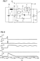
Figure 5 , thedevice 20 also includes an auxiliarycurrent path 32. In this instance, where the primary, secondary and tertiary current paths collectively define thebreaker circuit 22 in series with the dc circuit 7, the auxiliarycurrent path 32 is connected in parallel with thedc circuit 36. Asecond varistor 8 can then be connected in series with the auxiliarycurrent path 32 so as to be connected in parallel with the main current path serially connecting thebreaker circuit 22 and the dc circuit 7. - According to a third embodiment shown in
Figure 7 , thedevice 20 includes all of the features of the previous embodiment together with an additional auxiliarycurrent path 34 connected in parallel with the dc circuit 7. In this arrangement, the auxiliarycurrent path 34 and parallel connected dc current 7 are collectively connected in series with thebreaker circuit 22. Athird varistor 9 is connected in series with the auxiliarycurrent path 34 such that the third varistor is in parallel with the second dc circuit 7 and the collective parallel connection of the third varistor and the second dc circuit 7 is in series between thebreaker circuit 22 and the return path of the second dc circuit 7 to thefirst dc circuit 36. - Turning now to a fourth embodiment as shown in
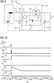
Figure 9 , in this instance, thedevice 20 includes all of the features of the previous embodiment along with an additionalauxiliary interrupter switch 10 connected in series with the main current path between thefirst dc circuit 36 and thebreaker circuit 22. Alternatively theauxiliary interrupter switch 10 may be connected in series with the maincurrent path 26 on the opposite side of thebreaker circuit 22 between thebreaker circuit 22 and the second dc circuit 7. The auxiliarycurrent path 32 connects in parallel with the main current path between thedc circuit 36 and theauxiliary interrupter switch 10. - In the fifth embodiment as shown in
Figure 11 , thedevice 20 includes all of the features of the previous embodiments with an additional fourthcurrent path 41 defining a supplementary current path connected in parallel to the primarycurrent path 24 and the secondarycurrent path 28 and the tertiarycurrent path 30 so that they are collectively in series with the maincurrent path 26. - A damping
resistor 39 and a dampinginductor 40 are connected in parallel to each other and collectively define a damping circuit which is connected in series to the fourthcurrent path 41. - Additionally a
switch 37 is connected in series with the fourthcurrent path 41 and the damping circuit formed by the parallel combination of the dampingresistor 39 and the dampinginductor 40. Theswitch 37 can be mechanical, electronic, spark gap, plasma injection, vacuum tube or any other device or combination of devices that is capable of closing the circuit upon receiving a command signal and opening the circuit either by a command signal or when its current or voltage is reduced below a threshold level. - Alternatively the damping circuit may consist of a damping
resistor 39 connected in series with a spark gap and a dampinginductor 40 connected in parallel to the series combination of the damping resistor and the spark gap. - The functioning of the various embodiments described above will now be described in further detail. As described above,
Figure 3 shows an electric circuit consisting of afirst dc circuit 36, amechanical interrupter switch 3, anelectronic breaker switch 4, acapacitor 5, avaristor 6 and the remaining parts of the dc circuit schematically shown as block 7. In this case thefirst dc circuit 36 consists of a source of dc current 1 and aninductor 2 that represents the inductance present in the circuit, however in general thefirst dc circuit 36 can consist of any busbars, overhead transmission lines, cables, reactors, breakers, converters or any other components. - The source 1 can be a battery, a dc generator or any kind of electronic ac to dc converter. The
reactor 2 represents the total inductance present between the source and the breaker. This includes any physical inductor and the inductance of the busbars, conductors and any stray inductances. - The
mechanical switch 3 can be a circuit breaker, a load switch or a fast disconnector. This mechanical switch will open at near zero dc voltage and current. Theelectronic breaker 4 is an electronic switch made of IGBT's, GTO's, GeT's, electron tubes or any other electronic components that is capable of being turned on and off by an electronic signal. The voltage rating of theauxiliary breaker 4 is lower than the rated voltage of the dc circuit. If the hybrid dc circuit breaker is required to break the dc current in both directions, the auxiliary electronic breaker must be capable of blocking current in both directions. The remaining parts of the dc circuit including any busbars, overhead transmission lines, cables, reactors, breakers, converters or any other components are schematically shown as block 7. - The current breaking principle of the new hybrid
dc breaker circuit 22 is explained here with reference toFigure 3 . When the hybrid dc breaker is closed themechanical switch 3 is closed and theelectronic breaker 4 is conducting. The voltage across thecapacitor 5 is equal to the voltage drop across themechanical switch 3 plus theelectronic breaker 4. Normally this voltage is very small compared to the rated voltage of the dc circuit. When the hybrid dc breaker is required to open a "turn off' order is sent to theelectronic breaker 4. Within a short time before or after theelectronic breaker 4 themechanical switch 3 is also ordered to open. As a result of the "turn off' order to the electronic breaker the resistance of this device is increased, which will cause the dc current to be commutated to thecapacitor 5. The capacitor voltage will start to rise at a rate related to its capacitance and the dc current intensity. The current flow through themechanical switch 3 is reduced to nearly zero, which
permits this device to open without any significant arcing. The voltage across thecapacitor 5 will continue to rise until the current flow is stopped. Thevaristor 6 protectscapacitor 5 from an overvoltage.Figure 4 shows the current and voltage waveforms for an example ease where a short circuit occurs between the dc conductors at a point between thehybrid de breaker 22 and the rest of the de circuit 7. - When the short circuit occurs the dc current through
mechanical switch 3 rises at a rate determined by the source 1 and theinductance 2. The first graph 1_3 inFigure 4 shows the current through themechanical switch 3. As explained above shortly after the hybrid breaker is ordered to open theelectronic breaker 4 is turned off causing the current to be commutated to thecapacitor 5. This will cause the capacitor voltage V_5 to grow up to the knee voltage of thevaristor 6. At this point varistor starts conducting and V_5 remains almost constant. The varistor knee voltage is higher than the voltage of the de source 1 by design, therefore the polarity of the voltage across theinductor 2 is such that the de current is diminished. InFigure 4 - 3 is the current through themechanical switch 3, 1_5 is the current through thecapacitor 5, 1_6 is the current through thevaristor 6 and V_5 is the voltage across thecapacitor 5. - As shown in the example above, in the hybrid dc breaker shown in
Figure 3 some current may flow through thevaristor 6 toward the dc circuit 7 for some time after themechanical switch 3 was opened. The magnitude and duration of this current depends on the parameters such as the capacitance of thecapacitor 5, the inductance of thereactor 2 and the knee voltage of thevaristor 6. The flow of the current through the varistor after opening the breaker may not be acceptable in some applications.Figure 5 shows a variation of the hybrid dc circuit breaker where avaristor 8 is added to the circuit. The knee voltage forvaristor 8 is selected below the knee voltage for thevaristor 6.Figure 6 shows the simulation results for a short circuit event similar to the case shown inFigure 4 . InFigure 6 all current and voltage designations are similar toFigure 4 , the new trace L8 represents the current through thevaristor 8.Figure 6 shows that the current through thevaristor 6 is reduced to almost zero in this arrangement. - The hybrid dc breaker can be designed to break the current in both directions as explained earlier. In this case for a short circuit fault that occurs at a point on the circuit between the hybrid dc breaker and the
first dc circuit 36, or within thefirst dc circuit 36, the behaviour of the hybrid dc breaker is similar to the previous cases discussed above. The rate of rise for the fault current will depend on the inductance of the complete fault current path in this case. Similar to the previous example the flow of current through thevaristor 6 may not be acceptable in some applications. A variation of the hybrid dc breaker shown inFigure 7 will reduce the current flow throughvaristor 6 to almost zero following a fault on either side of the breaker. - Depending on the characteristics of the
first dc circuit 36 and the second dc circuit 7 and the location of the fault, when the hybrid dc breaker is ordered to open the current through thecapacitor 5 may oscillate a number of times before settling at zero.Figure 8 shows an example of such possible situation. The flow of oscillatory current through the hybrid dc breaker's capacitor may not be acceptable in some applications. An embodiment of the dc hybrid breaker with an additionalauxiliary interrupter switch 10 as shown inFigure 9 is capable of avoiding such oscillatory currents. When the hybrid dc breaker is required to open theauxiliary interrupter switch 10 is ordered to open as well as themechanical switch 3 and theelectronic breaker 4. The residual breaker completely stops the dc current as soon as its current reach zero.Figure 10 shows the same example simulation case shown inFigure 8 , but with the embodiment of the hybrid dc breaker shown inFigure 9 . - Some applications may require a fast reclose of the dc circuit breaker to resume the flow of the dc current. The fifth embodiment shown in
Figure 11 allows a fast discharge of thecapacitor 5 and reclosing of themechanical interrupter switch 3 andelectronic breaker switch 4.Figure 12 shows a computer simulation example of the open and reclose procedure for the hybrid dc circuit breaker. The process of opening the dc breaker is similar to the process described in connection to the forth embodiment and the simulation example shown inFigure 10 . At the end of this process thecapacitor 5 is charged to the voltage V_5 as shown inFigure 12 . When a fast reclose is required theswitch 37 is ordered to close. This will provide a path forcapacitor 5 to discharge through the dampingresistor 39 and the dampinginductor 40. The resistance and inductance of these elements are selected such that thecapacitor 5 is discharged within the required time. Once the capacitor voltage and current are below acceptable threshold themechanical interrupter switch 3 andelectronic breaker switch 4 are ordered to close and the current flow through the breaker is resumed.
Claims (14)
- An arrangement comprising- a first DC circuit (36) with a first connection node and a second connection node;- a circuit breaking device (20) with a first connection node and a second connection node, wherein the circuit breaking device (20) is adapted to brake a DC component in the current path between its first and second connection nodes, and wherein the first connection node of the first DC circuit (36) is connected to the first connection node of the circuit breaking device (20);- a second DC circuit (7) with a first connection node and a second connection node the first connection node of the second DC circuit (7) being connected to the second connection node of the circuit breaking device (20), while the second connection node of the second DC circuit (7) is connected to the second connection node of the first DC circuit (36);said circuit breaking device (20) comprising- a mechanical interrupter switch (3) having contacts movable relative to each other between a closed position arranged to conduct current flowing there through and an open position arranged to break a current flowing there through;- an electronic breaker switch (4) connected in series with the mechanical interrupter switch (3) between the first and second connection nodes of the circuit breaking device, the electronic breaker switch being operable to open from a closed state arranged to conduct current flowing there through to an open state arranged to break a current flowing there through upon receipt of an electronic opening signal;- a capacitor (5) connected in parallel to the serially connected mechanical interrupter switch (3) and the electronic breaker switch (4);- a first varistor (6) connected in parallel to both the capacitor (5) and the serially connected mechanical interrupter switch (3) and the electronic breaker switch (4); and- a second varistor (8) connected in parallel to the first DC circuit (3) between the first and second connection nodes of the first DC circuit (3), wherein- a knee voltage of the second varistor (8) being less than a knee voltage of the first varistor (6).
- The arrangement according to Claim 1 wherein a rated voltage of the electronic breaker switch (4) is lower than a rated voltage of the first (36) and second dc circuits (7).
- The arrangement according to either one of Claims 1 or 2 further comprising a controller (18) arranged to order the electronic breaker switch (4) to open or close and to displace the mechanical switch (3) into the open position immediately subsequent to opening of the electronic breaker switch (4).
- The arrangement according to any one of Claims 1 through 3 further comprising a tertiary current path (30) connected in parallel, with a primary current path (24) and a secondary current path (28), and a varistor (6) connected in the tertiary current path (30) so as to be in parallel with the serially connected switches (3,4) and in parallel with the capacitor (5).
- The arrangement according to Claim 4 wherein the primary current path (24) and the secondary current path (28) define a breaker circuit (22) in series with the main current path (26), and wherein the device further comprises an auxiliary current path (32) connected in parallel with the first dc circuit (36), the auxiliary current path (32) including a varistor (8) connected in series therewith.
- The arrangement according to any one of Claims 4 through 5 wherein the primary current path (24) and the secondary current path (28) define a breaker circuit (22) in series with the main current path (26), and wherein the device further comprises:- a tertiary current path (30) connected in parallel with the primary current path (24) and the secondary current path (28) ;- a first varistor (6) connected in the tertiary current path (30) so as to be in parallel with the serially connected switches (3,4) and in parallel with the capacitor (5);- a first auxiliary current (32) path connected in parallel with the first dc circuit (36);- a second varistor (8) connected in the first auxiliary current path (32);- a second auxiliary current path (34) connected in parallel with the second dc circuit (7); and- a third varistor (9) connected in the second auxiliary current path (34).
- The arrangement according to any one of Claims 4 through 6 wherein the primary current path (24) and the secondary current path (28) define a breaker circuit (22) in series with the main current path (26), and wherein the device further comprises:- an auxiliary interrupter switch (10) connected in series between the breaker circuit (22) and one of the first (36) and second dc circuits (7).
- The arrangement according to any one of Claims 1 through 7 wherein the electronic breaker switch (4) comprises a solid state semiconductor based circuit breaker capable of interrupting current in only one direction.
- The arrangement according to any one of Claims 1 through 7 wherein the electronic breaker switch (4) comprises a solid state semiconductor based circuit breaker capable of interrupting current in both directions.
- The arrangement according to any one of Claims 1 through 7 wherein the electronic breaker switch (4) comprises a vacuum tube circuit breaker capable of interrupting current in only one direction.
- The arrangement according to any one of Claims 1 through 7 wherein the electronic breaker switch (4) comprises a vacuum tube circuit breaker capable of interrupting current in both directions.
- The arrangement according to any one of Claims 4 through 11 further comprising:- a supplementary current path (41) connected in parallel with the primary current path (24) and the secondary current path (28);- a damping circuit (39,40) connected in the supplementary current path (41); and- a supplementary switch (37) connected in series with the damping circuit (39,40) in the supplementary current path (41) in which the switch (37) is operable between a closed state arranged to conduct current flowing therethrough and an open state arranged to break a current flowing therethrough.
- The arrangement according to Claim 12 wherein the damping circuit comprises a damping resistor (39) and a damping inductor (40) connected in parallel with one another.
- The arrangement according to Claim 12 wherein the damping circuit comprises a damping resistor (39) connected in series with a spark gap and a damping inductor (40) connected in parallel to the serially connected damping resistor (39) and spark gap.
Applications Claiming Priority (3)
| Application Number | Priority Date | Filing Date | Title |
|---|---|---|---|
| US201161579336P | 2011-12-22 | 2011-12-22 | |
| US201261693842P | 2012-08-28 | 2012-08-28 | |
| PCT/EP2012/076782 WO2013093066A1 (en) | 2011-12-22 | 2012-12-21 | Hybrid dc circuit breaking device |
Publications (2)
| Publication Number | Publication Date |
|---|---|
| EP2777059A1 EP2777059A1 (en) | 2014-09-17 |
| EP2777059B1 true EP2777059B1 (en) | 2022-02-02 |
Family
ID=47553029
Family Applications (1)
| Application Number | Title | Priority Date | Filing Date |
|---|---|---|---|
| EP12813371.7A Active EP2777059B1 (en) | 2011-12-22 | 2012-12-21 | Hybrid dc circuit breaking device |
Country Status (5)
| Country | Link |
|---|---|
| US (1) | US20150022928A1 (en) |
| EP (1) | EP2777059B1 (en) |
| CA (1) | CA2860171C (en) |
| ES (1) | ES2911756T3 (en) |
| WO (1) | WO2013093066A1 (en) |
Cited By (1)
| Publication number | Priority date | Publication date | Assignee | Title |
|---|---|---|---|---|
| US11532442B2 (en) * | 2018-06-27 | 2022-12-20 | Uchiya Thermostat Co., Ltd. | Electronic device with case having sheath-piercing tapered sections |
Families Citing this family (52)
| Publication number | Priority date | Publication date | Assignee | Title |
|---|---|---|---|---|
| FR2977738B1 (en) * | 2011-07-04 | 2015-01-16 | Mersen France Sb Sas | CONTINUOUS CURRENT INTERRUPTION SYSTEM FOR OPENING INDUCTIVE CONTINUOUS CURRENT LINE |
| DE102011082568A1 (en) * | 2011-09-13 | 2013-03-14 | Siemens Aktiengesellschaft | DC circuit breaker |
| DE102011083693B3 (en) * | 2011-09-29 | 2013-03-28 | Siemens Aktiengesellschaft | DC circuit breaker |
| DE102012209903A1 (en) * | 2012-06-13 | 2013-12-19 | Siemens Aktiengesellschaft | Device for switching in a direct voltage network |
| CN103280763B (en) * | 2013-02-27 | 2016-12-28 | 国网智能电网研究院 | A kind of dc circuit breaker and its implementation |
| WO2015007621A1 (en) * | 2013-07-19 | 2015-01-22 | Alstom Technology Ltd | Voltage limiter |
| WO2015078525A1 (en) | 2013-11-29 | 2015-06-04 | Siemens Aktiengesellschaft | Device and method for switching a direct current |
| CN103632895B (en) * | 2013-12-04 | 2016-01-20 | 中国科学院电工研究所 | A kind of DC circuit breaker |
| US10056774B2 (en) * | 2014-02-06 | 2018-08-21 | Mitsubishi Electric Corporation | Discharge device |
| US20150272705A1 (en) * | 2014-03-28 | 2015-10-01 | Jason Watson | Dental device comprising surgical template and false teeth set and related methods |
| US9419539B2 (en) | 2014-08-25 | 2016-08-16 | General Electric Company | Systems and methods for enhanced operation and protection of power converters |
| JP6049957B2 (en) * | 2014-09-26 | 2016-12-21 | 三菱電機株式会社 | DC circuit breaker |
| KR101658539B1 (en) | 2014-10-10 | 2016-09-22 | 엘에스산전 주식회사 | Direct Current Circuit Breaker and Method Using The Same |
| EP3041015B1 (en) * | 2015-01-05 | 2020-03-25 | General Electric Technology GmbH | DC breaker |
| KR101766229B1 (en) | 2015-04-13 | 2017-08-09 | 한국전기연구원 | Apparatus and method for interrupting high voltage direct current using gap switch |
| EP4012738A1 (en) * | 2015-05-05 | 2022-06-15 | Siemens Aktiengesellschaft | Switching device |
| CN104993472A (en) * | 2015-08-07 | 2015-10-21 | 国网浙江省电力公司电力科学研究院 | MMC-HVDC system, DC side isolation device and isolation method |
| CN105305371B (en) * | 2015-11-14 | 2018-05-25 | 华中科技大学 | A High Voltage DC Circuit Breaker with Coupling Reactor |
| CN105656019B (en) * | 2016-01-26 | 2019-06-28 | 华中科技大学 | A capacitor charging type DC circuit breaker and its application |
| FR3049130B1 (en) * | 2016-03-16 | 2019-06-28 | Alstom Transport Technologies | ELECTRIC ENERGY CONVERSION SYSTEM, ELECTRIC ENERGY STORAGE APPARATUS, AND TRACTION CHAIN FOR A RAIL VEHICLE |
| KR102558677B1 (en) * | 2016-04-04 | 2023-07-21 | 엘에스일렉트릭(주) | Current circuit breaker |
| DE102016120070A1 (en) * | 2016-10-21 | 2018-04-26 | Eaton Industries (Austria) Gmbh | Low-voltage protection device |
| GB2557348B (en) * | 2016-12-08 | 2020-09-30 | Ge Aviat Systems Ltd | Power distribution system including a commutation device |
| EP4160640B1 (en) * | 2017-07-11 | 2025-10-22 | Mitsubishi Electric Corporation | Direct-current circuit breaker |
| CN108962647B (en) * | 2017-07-24 | 2021-08-27 | 广州市金矢电子有限公司 | DC arc-extinguishing device |
| CN107370130B (en) * | 2017-09-08 | 2019-04-16 | 国家电网公司 | A hybrid HVDC circuit breaker based on improved half-bridge sub-module and its control strategy |
| EP3676946B1 (en) * | 2017-09-25 | 2021-12-29 | Huawei Digital Power Technologies Co., Ltd. | Hybrid multilevel inverters |
| EP3540750B1 (en) * | 2018-03-16 | 2021-05-05 | ABB Power Grids Switzerland AG | Hvdc circuit breaker, hvdc switchyard, hvdc switchyard system, and hvdc grid |
| KR102185036B1 (en) * | 2018-04-30 | 2020-12-01 | 엘에스일렉트릭(주) | Circuit breaker control module |
| US11037749B2 (en) | 2018-05-04 | 2021-06-15 | Atom Power, Inc. | Selective coordination of solid-state circuit breakers and mechanical circuit breakers in electrical distribution systems |
| GB2574038A (en) * | 2018-05-24 | 2019-11-27 | Entrust Microgrid Llp | Two-stage switching mechanism for use in a DC circuit |
| GB201809140D0 (en) | 2018-06-04 | 2018-07-18 | Univ Court Of The Univ Of Aberdeen | Apparatus suitable for interrupting a direct current |
| US11245255B2 (en) * | 2018-06-11 | 2022-02-08 | Siemens Aktiengesellschaft | Solid-state circuit breaker and breaking method for solid-state circuit breaker |
| EP3654477A1 (en) * | 2018-11-15 | 2020-05-20 | Siemens Aktiengesellschaft | Electronic switch with surge protector |
| DE102019203508A1 (en) * | 2019-03-15 | 2020-09-17 | Leoni Bordnetz-Systeme Gmbh | Switching device and method for operating a switching device |
| CN113574623B (en) * | 2019-03-29 | 2024-06-25 | 西门子股份公司 | Hybrid circuit breaker, hybrid circuit breaking system and circuit breaking method |
| CN110048381A (en) * | 2019-04-23 | 2019-07-23 | 西安交通大学 | Dc circuit breaker and its application method based on the transfer of liquid arc voltage |
| US11322916B2 (en) * | 2019-06-13 | 2022-05-03 | Atom Power, Inc. | Solid-state circuit breaker with galvanic isolation |
| US11791620B2 (en) | 2019-09-03 | 2023-10-17 | Atom Power, Inc. | Solid-state circuit breaker with self-diagnostic, self-maintenance, and self-protection capabilities |
| WO2021046097A1 (en) | 2019-09-03 | 2021-03-11 | Atom Power, Inc. | Solid-state circuit breaker with self-diagnostic, self-maintenance, and self-protection capabilities |
| US11527878B2 (en) * | 2020-10-14 | 2022-12-13 | Eaton Intelligent Power Limited | Hybrid arc flash mitigation system |
| EP3989392B1 (en) | 2020-10-19 | 2026-04-22 | SolarEdge Technologies Ltd. | Power device terminal backup switch unit of an ups |
| CN115036891B (en) * | 2021-03-03 | 2025-08-01 | 南京南瑞继保电气有限公司 | Multiport hybrid DC circuit breaker and control method thereof |
| KR102652768B1 (en) * | 2021-03-29 | 2024-04-01 | 엘에스일렉트릭(주) | Bpu(battery protection unit) and method for controlling thereof |
| CN113824083B (en) * | 2021-07-09 | 2022-10-18 | 天津大学 | Hybrid direct current breaker with self-adaptive reclosing |
| GB202115513D0 (en) | 2021-10-28 | 2021-12-15 | Rolls Royce Plc | Electrical power system |
| US11798756B2 (en) | 2022-01-18 | 2023-10-24 | Siemens Industry, Inc. | Solid-state circuit breaker trips an air gap actuator and solid-state switching components at the same time or the solid-state switching components with a delay |
| GB2615554A (en) * | 2022-02-11 | 2023-08-16 | Eaton Intelligent Power Ltd | Hybrid circuit breaker |
| KR102824916B1 (en) * | 2022-10-06 | 2025-06-24 | 가부시키가이샤 티마이크 | Power supply |
| US20240195166A1 (en) * | 2022-12-13 | 2024-06-13 | Battelle Memorial Institute | Circuit Breakers and Circuit Breaker Operational Methods |
| US12469661B2 (en) * | 2023-03-21 | 2025-11-11 | Siemens Industry, Inc. | DC solid-state circuit breaker with fail-safe redundancy via double power electronics and overvoltage protection |
| US20250300453A1 (en) * | 2024-03-21 | 2025-09-25 | Abb Schweiz Ag | Voltage Clamping Circuit for Solid State Circuit Breakers |
Citations (1)
| Publication number | Priority date | Publication date | Assignee | Title |
|---|---|---|---|---|
| US5517378A (en) * | 1993-12-09 | 1996-05-14 | Asea Brown Boveri Ab | Direct-current breaker for high power for connection into a direct-current carrying high-voltage line |
Family Cites Families (9)
| Publication number | Priority date | Publication date | Assignee | Title |
|---|---|---|---|---|
| US3497771A (en) * | 1967-05-31 | 1970-02-24 | Nokia Oy Ab | Series capacitor protector using damping resistor coil combination |
| US3814878A (en) * | 1970-03-31 | 1974-06-04 | Porter Co H | Circuit breaker operating mechanism |
| US3781606A (en) * | 1972-12-11 | 1973-12-25 | Hughes Aircraft Co | Circuit breaker and method |
| US5666257A (en) * | 1994-10-18 | 1997-09-09 | Yang; Tai-Her | DC circuit breaking spark suppressor circuit device |
| EP1538645B1 (en) * | 2003-12-05 | 2006-03-01 | Société Technique pour l'Energie Atomique TECHNICATOME | Hybrid circuit breaker |
| US20060067021A1 (en) * | 2004-09-27 | 2006-03-30 | Xiang-Ming Li | Over-voltage and over-current protection device |
| US7397222B2 (en) * | 2006-08-30 | 2008-07-08 | Westinghouse Electric Co Llc | On-line testable solid state reversing DC motor starter |
| WO2011057675A1 (en) * | 2009-11-16 | 2011-05-19 | Abb Technology Ag | Device and method to break the current of a power transmission or distribution line and current limiting arrangement |
| WO2011141055A1 (en) * | 2010-05-11 | 2011-11-17 | Abb Technology Ag | A high voltage dc breaker apparatus |
-
2012
- 2012-12-21 CA CA2860171A patent/CA2860171C/en active Active
- 2012-12-21 EP EP12813371.7A patent/EP2777059B1/en active Active
- 2012-12-21 US US14/367,991 patent/US20150022928A1/en not_active Abandoned
- 2012-12-21 ES ES12813371T patent/ES2911756T3/en active Active
- 2012-12-21 WO PCT/EP2012/076782 patent/WO2013093066A1/en not_active Ceased
Patent Citations (1)
| Publication number | Priority date | Publication date | Assignee | Title |
|---|---|---|---|---|
| US5517378A (en) * | 1993-12-09 | 1996-05-14 | Asea Brown Boveri Ab | Direct-current breaker for high power for connection into a direct-current carrying high-voltage line |
Cited By (1)
| Publication number | Priority date | Publication date | Assignee | Title |
|---|---|---|---|---|
| US11532442B2 (en) * | 2018-06-27 | 2022-12-20 | Uchiya Thermostat Co., Ltd. | Electronic device with case having sheath-piercing tapered sections |
Also Published As
| Publication number | Publication date |
|---|---|
| CA2860171A1 (en) | 2013-06-27 |
| ES2911756T3 (en) | 2022-05-20 |
| CA2860171C (en) | 2021-09-21 |
| WO2013093066A1 (en) | 2013-06-27 |
| US20150022928A1 (en) | 2015-01-22 |
| EP2777059A1 (en) | 2014-09-17 |
Similar Documents
| Publication | Publication Date | Title |
|---|---|---|
| EP2777059B1 (en) | Hybrid dc circuit breaking device | |
| CN104756338B (en) | Circuit interrupting equipment | |
| KR101521545B1 (en) | Device and method to interrupt high voltage direct current | |
| EP3107172B1 (en) | Protection system for dc power transmission system, ac/dc converter, and dc power transmission system breaking method | |
| CN104756339B (en) | Circuit interrupting equipment | |
| US9373473B2 (en) | Mechatronic circuit breaker device and associated tripping method and use thereof in interrupting a high direct current | |
| Raghavendra et al. | Modified Z-source DC circuit breaker with enhanced performance during commissioning and reclosing | |
| US9478974B2 (en) | DC voltage circuit breaker | |
| EP3093941B1 (en) | Direct current circuit breaker and method using the same | |
| US6075684A (en) | Method and arrangement for direct current circuit interruption | |
| EP0532045B1 (en) | Electrical power supply system | |
| US20150131189A1 (en) | Composite high voltage dc circuit breaker | |
| US20140226247A1 (en) | Dc voltage line circuit breaker | |
| EP3157034B1 (en) | Mechatronic circuit-breaker device | |
| EP3803929B1 (en) | High voltage direct current (hvdc) circuit breaker | |
| Heidemann et al. | Circuit-breakers for medium-voltage DC grids | |
| Martinez et al. | EMTP modeling of hybrid HVDC breakers | |
| Jehle et al. | Hybrid circuit breaker for HVDC grids with controllable pulse current shape | |
| Augustin et al. | Modelling of HVDC breakers for HVDC grid simulations | |
| Qawasmi et al. | A comparison of circuit breaker technologies for medium voltage direct current distribution networks | |
| Kim et al. | Modular hybrid DC circuit breaker for medium-voltage DC system | |
| Zhou et al. | Design and performance of a capacitor commutated DC circuit breaker |
Legal Events
| Date | Code | Title | Description |
|---|---|---|---|
| PUAI | Public reference made under article 153(3) epc to a published international application that has entered the european phase |
Free format text: ORIGINAL CODE: 0009012 |
|
| 17P | Request for examination filed |
Effective date: 20140613 |
|
| AK | Designated contracting states |
Kind code of ref document: A1 Designated state(s): AL AT BE BG CH CY CZ DE DK EE ES FI FR GB GR HR HU IE IS IT LI LT LU LV MC MK MT NL NO PL PT RO RS SE SI SK SM TR |
|
| DAX | Request for extension of the european patent (deleted) | ||
| STAA | Information on the status of an ep patent application or granted ep patent |
Free format text: STATUS: EXAMINATION IS IN PROGRESS |
|
| 17Q | First examination report despatched |
Effective date: 20170713 |
|
| RAP1 | Party data changed (applicant data changed or rights of an application transferred) |
Owner name: SIEMENS AKTIENGESELLSCHAFT |
|
| RAP1 | Party data changed (applicant data changed or rights of an application transferred) |
Owner name: SIEMENS ENERGY GLOBAL GMBH & CO. KG |
|
| GRAP | Despatch of communication of intention to grant a patent |
Free format text: ORIGINAL CODE: EPIDOSNIGR1 |
|
| STAA | Information on the status of an ep patent application or granted ep patent |
Free format text: STATUS: GRANT OF PATENT IS INTENDED |
|
| INTG | Intention to grant announced |
Effective date: 20210721 |
|
| GRAS | Grant fee paid |
Free format text: ORIGINAL CODE: EPIDOSNIGR3 |
|
| GRAA | (expected) grant |
Free format text: ORIGINAL CODE: 0009210 |
|
| STAA | Information on the status of an ep patent application or granted ep patent |
Free format text: STATUS: THE PATENT HAS BEEN GRANTED |
|
| AK | Designated contracting states |
Kind code of ref document: B1 Designated state(s): AL AT BE BG CH CY CZ DE DK EE ES FI FR GB GR HR HU IE IS IT LI LT LU LV MC MK MT NL NO PL PT RO RS SE SI SK SM TR |
|
| REG | Reference to a national code |
Ref country code: GB Ref legal event code: FG4D |
|
| REG | Reference to a national code |
Ref country code: CH Ref legal event code: EP Ref country code: AT Ref legal event code: REF Ref document number: 1466802 Country of ref document: AT Kind code of ref document: T Effective date: 20220215 |
|
| REG | Reference to a national code |
Ref country code: DE Ref legal event code: R096 Ref document number: 602012077623 Country of ref document: DE |
|
| REG | Reference to a national code |
Ref country code: IE Ref legal event code: FG4D |
|
| REG | Reference to a national code |
Ref country code: SE Ref legal event code: TRGR |
|
| REG | Reference to a national code |
Ref country code: ES Ref legal event code: FG2A Ref document number: 2911756 Country of ref document: ES Kind code of ref document: T3 Effective date: 20220520 |
|
| REG | Reference to a national code |
Ref country code: LT Ref legal event code: MG9D |
|
| REG | Reference to a national code |
Ref country code: NL Ref legal event code: MP Effective date: 20220202 |
|
| REG | Reference to a national code |
Ref country code: AT Ref legal event code: MK05 Ref document number: 1466802 Country of ref document: AT Kind code of ref document: T Effective date: 20220202 |
|
| PG25 | Lapsed in a contracting state [announced via postgrant information from national office to epo] |
Ref country code: RS Free format text: LAPSE BECAUSE OF FAILURE TO SUBMIT A TRANSLATION OF THE DESCRIPTION OR TO PAY THE FEE WITHIN THE PRESCRIBED TIME-LIMIT Effective date: 20220202 Ref country code: PT Free format text: LAPSE BECAUSE OF FAILURE TO SUBMIT A TRANSLATION OF THE DESCRIPTION OR TO PAY THE FEE WITHIN THE PRESCRIBED TIME-LIMIT Effective date: 20220602 Ref country code: NO Free format text: LAPSE BECAUSE OF FAILURE TO SUBMIT A TRANSLATION OF THE DESCRIPTION OR TO PAY THE FEE WITHIN THE PRESCRIBED TIME-LIMIT Effective date: 20220502 Ref country code: NL Free format text: LAPSE BECAUSE OF FAILURE TO SUBMIT A TRANSLATION OF THE DESCRIPTION OR TO PAY THE FEE WITHIN THE PRESCRIBED TIME-LIMIT Effective date: 20220202 Ref country code: LT Free format text: LAPSE BECAUSE OF FAILURE TO SUBMIT A TRANSLATION OF THE DESCRIPTION OR TO PAY THE FEE WITHIN THE PRESCRIBED TIME-LIMIT Effective date: 20220202 Ref country code: HR Free format text: LAPSE BECAUSE OF FAILURE TO SUBMIT A TRANSLATION OF THE DESCRIPTION OR TO PAY THE FEE WITHIN THE PRESCRIBED TIME-LIMIT Effective date: 20220202 Ref country code: BG Free format text: LAPSE BECAUSE OF FAILURE TO SUBMIT A TRANSLATION OF THE DESCRIPTION OR TO PAY THE FEE WITHIN THE PRESCRIBED TIME-LIMIT Effective date: 20220502 |
|
| PG25 | Lapsed in a contracting state [announced via postgrant information from national office to epo] |
Ref country code: PL Free format text: LAPSE BECAUSE OF FAILURE TO SUBMIT A TRANSLATION OF THE DESCRIPTION OR TO PAY THE FEE WITHIN THE PRESCRIBED TIME-LIMIT Effective date: 20220202 Ref country code: LV Free format text: LAPSE BECAUSE OF FAILURE TO SUBMIT A TRANSLATION OF THE DESCRIPTION OR TO PAY THE FEE WITHIN THE PRESCRIBED TIME-LIMIT Effective date: 20220202 Ref country code: GR Free format text: LAPSE BECAUSE OF FAILURE TO SUBMIT A TRANSLATION OF THE DESCRIPTION OR TO PAY THE FEE WITHIN THE PRESCRIBED TIME-LIMIT Effective date: 20220503 Ref country code: FI Free format text: LAPSE BECAUSE OF FAILURE TO SUBMIT A TRANSLATION OF THE DESCRIPTION OR TO PAY THE FEE WITHIN THE PRESCRIBED TIME-LIMIT Effective date: 20220202 Ref country code: AT Free format text: LAPSE BECAUSE OF FAILURE TO SUBMIT A TRANSLATION OF THE DESCRIPTION OR TO PAY THE FEE WITHIN THE PRESCRIBED TIME-LIMIT Effective date: 20220202 |
|
| PG25 | Lapsed in a contracting state [announced via postgrant information from national office to epo] |
Ref country code: IS Free format text: LAPSE BECAUSE OF FAILURE TO SUBMIT A TRANSLATION OF THE DESCRIPTION OR TO PAY THE FEE WITHIN THE PRESCRIBED TIME-LIMIT Effective date: 20220602 |
|
| PG25 | Lapsed in a contracting state [announced via postgrant information from national office to epo] |
Ref country code: SM Free format text: LAPSE BECAUSE OF FAILURE TO SUBMIT A TRANSLATION OF THE DESCRIPTION OR TO PAY THE FEE WITHIN THE PRESCRIBED TIME-LIMIT Effective date: 20220202 Ref country code: SK Free format text: LAPSE BECAUSE OF FAILURE TO SUBMIT A TRANSLATION OF THE DESCRIPTION OR TO PAY THE FEE WITHIN THE PRESCRIBED TIME-LIMIT Effective date: 20220202 Ref country code: RO Free format text: LAPSE BECAUSE OF FAILURE TO SUBMIT A TRANSLATION OF THE DESCRIPTION OR TO PAY THE FEE WITHIN THE PRESCRIBED TIME-LIMIT Effective date: 20220202 Ref country code: EE Free format text: LAPSE BECAUSE OF FAILURE TO SUBMIT A TRANSLATION OF THE DESCRIPTION OR TO PAY THE FEE WITHIN THE PRESCRIBED TIME-LIMIT Effective date: 20220202 Ref country code: DK Free format text: LAPSE BECAUSE OF FAILURE TO SUBMIT A TRANSLATION OF THE DESCRIPTION OR TO PAY THE FEE WITHIN THE PRESCRIBED TIME-LIMIT Effective date: 20220202 Ref country code: CZ Free format text: LAPSE BECAUSE OF FAILURE TO SUBMIT A TRANSLATION OF THE DESCRIPTION OR TO PAY THE FEE WITHIN THE PRESCRIBED TIME-LIMIT Effective date: 20220202 |
|
| REG | Reference to a national code |
Ref country code: DE Ref legal event code: R097 Ref document number: 602012077623 Country of ref document: DE |
|
| PG25 | Lapsed in a contracting state [announced via postgrant information from national office to epo] |
Ref country code: AL Free format text: LAPSE BECAUSE OF FAILURE TO SUBMIT A TRANSLATION OF THE DESCRIPTION OR TO PAY THE FEE WITHIN THE PRESCRIBED TIME-LIMIT Effective date: 20220202 |
|
| PLBE | No opposition filed within time limit |
Free format text: ORIGINAL CODE: 0009261 |
|
| STAA | Information on the status of an ep patent application or granted ep patent |
Free format text: STATUS: NO OPPOSITION FILED WITHIN TIME LIMIT |
|
| 26N | No opposition filed |
Effective date: 20221103 |
|
| PG25 | Lapsed in a contracting state [announced via postgrant information from national office to epo] |
Ref country code: SI Free format text: LAPSE BECAUSE OF FAILURE TO SUBMIT A TRANSLATION OF THE DESCRIPTION OR TO PAY THE FEE WITHIN THE PRESCRIBED TIME-LIMIT Effective date: 20220202 |
|
| REG | Reference to a national code |
Ref country code: CH Ref legal event code: PL |
|
| REG | Reference to a national code |
Ref country code: BE Ref legal event code: MM Effective date: 20221231 |
|
| PG25 | Lapsed in a contracting state [announced via postgrant information from national office to epo] |
Ref country code: LU Free format text: LAPSE BECAUSE OF NON-PAYMENT OF DUE FEES Effective date: 20221221 |
|
| PG25 | Lapsed in a contracting state [announced via postgrant information from national office to epo] |
Ref country code: LI Free format text: LAPSE BECAUSE OF NON-PAYMENT OF DUE FEES Effective date: 20221231 Ref country code: IE Free format text: LAPSE BECAUSE OF NON-PAYMENT OF DUE FEES Effective date: 20221221 Ref country code: CH Free format text: LAPSE BECAUSE OF NON-PAYMENT OF DUE FEES Effective date: 20221231 |
|
| PG25 | Lapsed in a contracting state [announced via postgrant information from national office to epo] |
Ref country code: BE Free format text: LAPSE BECAUSE OF NON-PAYMENT OF DUE FEES Effective date: 20221231 |
|
| P01 | Opt-out of the competence of the unified patent court (upc) registered |
Effective date: 20231222 |
|
| PG25 | Lapsed in a contracting state [announced via postgrant information from national office to epo] |
Ref country code: HU Free format text: LAPSE BECAUSE OF FAILURE TO SUBMIT A TRANSLATION OF THE DESCRIPTION OR TO PAY THE FEE WITHIN THE PRESCRIBED TIME-LIMIT; INVALID AB INITIO Effective date: 20121221 |
|
| PG25 | Lapsed in a contracting state [announced via postgrant information from national office to epo] |
Ref country code: CY Free format text: LAPSE BECAUSE OF FAILURE TO SUBMIT A TRANSLATION OF THE DESCRIPTION OR TO PAY THE FEE WITHIN THE PRESCRIBED TIME-LIMIT Effective date: 20220202 |
|
| PG25 | Lapsed in a contracting state [announced via postgrant information from national office to epo] |
Ref country code: MK Free format text: LAPSE BECAUSE OF FAILURE TO SUBMIT A TRANSLATION OF THE DESCRIPTION OR TO PAY THE FEE WITHIN THE PRESCRIBED TIME-LIMIT Effective date: 20220202 |
|
| PG25 | Lapsed in a contracting state [announced via postgrant information from national office to epo] |
Ref country code: MC Free format text: LAPSE BECAUSE OF FAILURE TO SUBMIT A TRANSLATION OF THE DESCRIPTION OR TO PAY THE FEE WITHIN THE PRESCRIBED TIME-LIMIT Effective date: 20220202 |
|
| PG25 | Lapsed in a contracting state [announced via postgrant information from national office to epo] |
Ref country code: TR Free format text: LAPSE BECAUSE OF FAILURE TO SUBMIT A TRANSLATION OF THE DESCRIPTION OR TO PAY THE FEE WITHIN THE PRESCRIBED TIME-LIMIT Effective date: 20220202 Ref country code: MC Free format text: LAPSE BECAUSE OF FAILURE TO SUBMIT A TRANSLATION OF THE DESCRIPTION OR TO PAY THE FEE WITHIN THE PRESCRIBED TIME-LIMIT Effective date: 20220202 |
|
| PG25 | Lapsed in a contracting state [announced via postgrant information from national office to epo] |
Ref country code: MT Free format text: LAPSE BECAUSE OF FAILURE TO SUBMIT A TRANSLATION OF THE DESCRIPTION OR TO PAY THE FEE WITHIN THE PRESCRIBED TIME-LIMIT Effective date: 20220202 |
|
| PGFP | Annual fee paid to national office [announced via postgrant information from national office to epo] |
Ref country code: GB Payment date: 20251223 Year of fee payment: 14 |
|
| PGFP | Annual fee paid to national office [announced via postgrant information from national office to epo] |
Ref country code: IT Payment date: 20251218 Year of fee payment: 14 |
|
| PGFP | Annual fee paid to national office [announced via postgrant information from national office to epo] |
Ref country code: FR Payment date: 20251223 Year of fee payment: 14 |
|
| PGFP | Annual fee paid to national office [announced via postgrant information from national office to epo] |
Ref country code: SE Payment date: 20251222 Year of fee payment: 14 |
|
| PGFP | Annual fee paid to national office [announced via postgrant information from national office to epo] |
Ref country code: ES Payment date: 20260122 Year of fee payment: 14 |
|
| PGFP | Annual fee paid to national office [announced via postgrant information from national office to epo] |
Ref country code: DE Payment date: 20251229 Year of fee payment: 14 |