WO2024122343A1 - 半導体装置 - Google Patents
半導体装置 Download PDFInfo
- Publication number
- WO2024122343A1 WO2024122343A1 PCT/JP2023/041986 JP2023041986W WO2024122343A1 WO 2024122343 A1 WO2024122343 A1 WO 2024122343A1 JP 2023041986 W JP2023041986 W JP 2023041986W WO 2024122343 A1 WO2024122343 A1 WO 2024122343A1
- Authority
- WO
- WIPO (PCT)
- Prior art keywords
- semiconductor device
- sub
- metal
- connection
- electrode
- Prior art date
- Legal status (The legal status is an assumption and is not a legal conclusion. Google has not performed a legal analysis and makes no representation as to the accuracy of the status listed.)
- Ceased
Links
Images


Classifications
-
- H—ELECTRICITY
- H05—ELECTRIC TECHNIQUES NOT OTHERWISE PROVIDED FOR
- H05K—PRINTED CIRCUITS; CASINGS OR CONSTRUCTIONAL DETAILS OF ELECTRIC APPARATUS; MANUFACTURE OF ASSEMBLAGES OF ELECTRICAL COMPONENTS
- H05K13/00—Apparatus or processes specially adapted for manufacturing or adjusting assemblages of electric components
- H05K13/04—Mounting of components, e.g. of leadless components
-
- H—ELECTRICITY
- H10—SEMICONDUCTOR DEVICES; ELECTRIC SOLID-STATE DEVICES NOT OTHERWISE PROVIDED FOR
- H10W—GENERIC PACKAGES, INTERCONNECTIONS, CONNECTORS OR OTHER CONSTRUCTIONAL DETAILS OF DEVICES COVERED BY CLASS H10
- H10W40/00—Arrangements for thermal protection or thermal control
-
- H—ELECTRICITY
- H10—SEMICONDUCTOR DEVICES; ELECTRIC SOLID-STATE DEVICES NOT OTHERWISE PROVIDED FOR
- H10W—GENERIC PACKAGES, INTERCONNECTIONS, CONNECTORS OR OTHER CONSTRUCTIONAL DETAILS OF DEVICES COVERED BY CLASS H10
- H10W72/00—Interconnections or connectors in packages
- H10W72/071—Connecting or disconnecting
-
- H—ELECTRICITY
- H10—SEMICONDUCTOR DEVICES; ELECTRIC SOLID-STATE DEVICES NOT OTHERWISE PROVIDED FOR
- H10W—GENERIC PACKAGES, INTERCONNECTIONS, CONNECTORS OR OTHER CONSTRUCTIONAL DETAILS OF DEVICES COVERED BY CLASS H10
- H10W90/00—Package configurations
Definitions
- This disclosure relates to a semiconductor device.
- Patent Document 1 discloses forming a temperature detection element in a power transistor formation region in the vicinity of the transistor pad.
- Patent Document 2 discloses a semiconductor device in which a temperature detection element is arranged so as to be in contact with an insulating layer in the vicinity of the semiconductor element.
- the temperature is detected based on the heat transmitted through the mounting layer on which the semiconductor element is mounted and the insulating layer, so the accuracy of the detected temperature of the semiconductor element is reduced.
- An object of the present disclosure is to provide a semiconductor device that is an improvement over conventional semiconductor devices.
- an object of the present disclosure is to provide a semiconductor device that can improve the accuracy of the temperature of a semiconductor element that is detected without forming a temperature sensor inside the semiconductor element.
- the semiconductor device provided by the first aspect of the present disclosure includes a semiconductor element having a main surface and a back surface of the element facing opposite each other in the thickness direction, and a first electrode arranged on the main surface of the element, a first wire including a first metal, a second wire including a second metal having a thermoelectric power different from that of the first metal and having a first end and a second end farther from the semiconductor element than the first end, a metal part including a third metal arranged so as to transmit heat from the semiconductor element and to which the first wire and the second wire are joined, a wire junction part to which the second end of the second wire is joined, and a reference temperature detection part arranged closer to the second end than the semiconductor element and detecting a reference temperature of the wire junction part, and at least one of the first wire and the second wire is directly joined to the metal part.
- the semiconductor device provided by the second aspect of the present disclosure comprises a switching element arranged on a first side in the thickness direction and having a first electrode through which a main current flows, a metal part having a metal part main surface facing the first side in the thickness direction and arranged so that heat from the switching element is transferred, and a first sub-connecting member and a second sub-connecting member directly bonded to the metal part main surface, the first sub-connecting member is made of a first sub-metal and has a first connection part bonded to the metal part main surface, the second sub-connecting member is made of a second sub-metal having a thermoelectric power different from that of the first sub-metal and has a second connection part bonded to the metal part main surface, and the gradient of the potential difference in the direction in which the first connection part and the second connection part are aligned on the metal part main surface when electricity is applied and the main current flows through the first electrode is smaller than the gradient of the potential difference in the perpendicular direction.
- the above configuration can improve the accuracy of the detected temperature of the semiconductor element without forming a temperature sensor inside the semiconductor element.
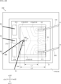
- FIG. 1 is a perspective view showing a semiconductor device according to a first embodiment of the present disclosure.
- FIG. 2 is a plan view of the semiconductor device shown in FIG. 1, seen through a resin member.
- FIG. 3 is a partially enlarged view of a part of FIG.
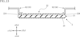
- FIG. 4 is a cross-sectional view taken along line IV-IV in FIG.
- FIG. 5 is a cross-sectional view taken along line VV in FIG.
- FIG. 6 is a cross-sectional view taken along line VI-VI in FIG.
- FIG. 7 is a cross-sectional view taken along line VII-VII in FIG.
- FIG. 8 is a perspective view showing a state in which a driving device is attached to the semiconductor device shown in FIG. FIG.
- FIG. 9 is a circuit diagram showing an example of a circuit configuration of the semiconductor device shown in FIG.
- FIG. 10 is a flowchart showing an example of a method for manufacturing the semiconductor device shown in FIG. 11A to 11C are cross-sectional views showing steps according to an example of a method for manufacturing the semiconductor device shown in FIG. 12A to 12C are cross-sectional views showing steps according to an example of a method for manufacturing the semiconductor device shown in FIG. 13A to 13C are cross-sectional views showing steps according to an example of a method for manufacturing the semiconductor device shown in FIG. 14A to 14C are cross-sectional views showing steps according to an example of a method for manufacturing the semiconductor device shown in FIG.
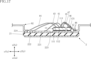
- FIG. 15 is an enlarged plan view showing a process according to an example of a method for manufacturing the semiconductor device shown in FIG. 16A to 16C are cross-sectional views showing steps according to an example of a method for manufacturing the semiconductor device shown in FIG. 17A to 17C are cross-sectional views showing steps according to an example of a method for manufacturing the semiconductor device shown in FIG.
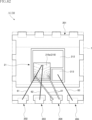
- FIG. 18 is a partial enlarged plan view showing a semiconductor device according to a first modification of the first embodiment.
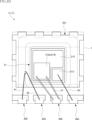
- FIG. 19 is a partial enlarged plan view showing a semiconductor device according to a second modification of the first embodiment.
- FIG. 20 is a partial enlarged plan view showing a semiconductor device according to a third modification of the first embodiment.
- FIG. 21 is a partial enlarged plan view showing a semiconductor device according to a fourth modification of the first embodiment.
- FIG. 22 is a cross-sectional view showing a semiconductor device according to a second embodiment of the present disclosure.
- 23 is a partial enlarged plan view showing the semiconductor device shown in FIG. 22.
- FIG. 24 is a partial enlarged plan view showing a semiconductor device according to a first modification of the second embodiment.
- FIG. 25 is a partial enlarged plan view showing a semiconductor device according to a third embodiment of the present disclosure.
- FIG. 26 is a partial enlarged plan view showing a semiconductor device according to a first modification of the third embodiment.
- FIG. 27 is a partial enlarged plan view showing a semiconductor device according to a fourth embodiment of the present disclosure.
- FIG. 22 is a cross-sectional view showing a semiconductor device according to a second embodiment of the present disclosure.
- 23 is a partial enlarged plan view showing the semiconductor device shown in FIG. 22.
- FIG. 24 is a partial enlarged
- FIG. 28 is a partial enlarged plan view showing a semiconductor device according to a first modification of the fourth embodiment.
- FIG. 29 is a partial enlarged plan view showing a semiconductor device according to a fifth embodiment of the present disclosure.
- FIG. 30 is a partial enlarged plan view showing a semiconductor device according to a first modification of the fifth embodiment.
- FIG. 31 is a partial enlarged plan view showing a semiconductor device according to a sixth embodiment of the present disclosure.
- 32 is a cross-sectional view taken along line XXXII-XXXII in FIG. 31.
- FIG. FIG. 33 is a circuit diagram showing an example of a circuit configuration of the semiconductor device shown in FIG. FIG.
- FIG. 34 is a circuit diagram showing an example of a circuit configuration of a semiconductor device according to a seventh embodiment of the present disclosure.
- FIG. 35 is a plan view showing a semiconductor device according to an eighth embodiment of the present disclosure, seen through a resin member.
- FIG. 36 is a plan view showing a semiconductor device according to a first modification of the eighth embodiment, seen through a resin member.
- FIG. 37 is a plan view showing a semiconductor device according to the ninth embodiment of the present disclosure.
- FIG. 38 is a bottom view showing the semiconductor device according to the ninth embodiment of the present disclosure.
- FIG. 39 is a side view showing a semiconductor device according to the ninth embodiment of the present disclosure.
- FIG. 40 is a cross-sectional view taken along line XL-XL in FIG.
- FIG. 41 is a cross-sectional view taken along line XLI-XLI in FIG.
- FIG. 42 is a cross-sectional view taken along line XLII-XLII in FIG.
- FIG. 43 is a cross-sectional view taken along line XLIII-XLIII in FIG.
- FIG. 44 is a cross-sectional view taken along line XLIV-XLIV in FIG.
- FIG. 41 is a cross-sectional view taken along line XLI-XLI in FIG.
- FIG. 42 is a cross-sectional view taken along line XLII-XLII in FIG.
- FIG. 43 is a cross-sectional view taken along line XLIII-X
- FIG. 48 is a plan view of a main portion showing a semiconductor device according to a ninth embodiment of the present disclosure.
- FIG. 49 is a plan view of a main portion showing a semiconductor device according to a ninth embodiment of the present disclosure.
- FIG. 50 is an enlarged plan view of a main portion showing a semiconductor device according to a ninth embodiment of the present disclosure.
- FIG. 51 is an enlarged plan view of a main portion showing a semiconductor device according to a ninth embodiment of the present disclosure.
- FIG. 52 is an enlarged plan view of a main portion showing a semiconductor device according to a first modified example of the ninth embodiment of the present disclosure.
- FIG. 53 is an enlarged plan view of a main portion showing a semiconductor device according to a second modification of the ninth embodiment of the present disclosure.
- FIG. 54 is an enlarged plan view of a main portion showing a semiconductor device according to a third modification of the ninth embodiment of the present disclosure.
- FIG. 55 is an enlarged plan view of a main portion showing a semiconductor device according to a fourth modification of the ninth embodiment of the present disclosure.
- FIG. 56 is an enlarged plan view of a main portion showing a semiconductor device according to a fifth modification of the ninth embodiment of the present disclosure.
- FIG. 57 is a plan view showing a semiconductor device according to the tenth embodiment of the present disclosure.
- FIG. 58 is a plan view of a main portion showing a semiconductor device according to a tenth embodiment of the present disclosure.
- FIG. 59 is a plan view of a main portion showing a semiconductor device according to an eleventh embodiment of the present disclosure.
- FIG. 60 is a plan view of a main portion showing a semiconductor device according to a twelfth embodiment of the present disclosure.
- FIG. 61 is an enlarged plan view of a main portion showing a semiconductor device according to a twelfth embodiment of the present disclosure.
- FIG. 62 is a plan view showing a semiconductor device according to the thirteenth embodiment of the present disclosure.
- FIG. 63 is a plan view showing a semiconductor device according to a first modification of the thirteenth embodiment of the present disclosure.
- first group shown in Figures 1 to 36 and the reference symbols (second group) shown in Figures 37 to 63 are used independently of each other.
- the reference symbol does not necessarily indicate the same component (or a similar component).
- these two reference symbols may indicate the same component (or a similar component).
- an object A is formed on an object B" and “an object A is formed on an object B” include “an object A is formed directly on an object B” and “an object A is formed on an object B with another object interposed between the object A and the object B” unless otherwise specified.
- an object A is disposed on an object B” and “an object A is disposed on an object B” include “an object A is disposed directly on an object B” and “an object A is disposed on an object B with another object interposed between the object A and the object B" unless otherwise specified.
- an object A is located on an object B includes “an object A is located on an object B in contact with an object B” and “an object A is located on an object B with another object interposed between the object A and the object B” unless otherwise specified.
- an object A overlaps an object B when viewed in a certain direction includes “an object A overlaps the entire object B” and “an object A overlaps a part of an object B.”
- a surface A faces in direction B is not limited to the case where the angle of surface A with respect to direction B is 90°, but also includes the case where surface A is tilted with respect to direction B.
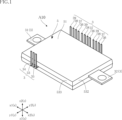
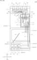
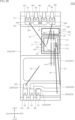
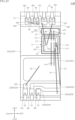
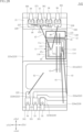
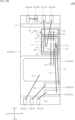
- the semiconductor device A10 may include a plurality of semiconductor elements 11, a plurality of semiconductor elements 12, a plurality of temperature sensors 15, a support member 2, a plurality of terminals 3, a plurality of connection members 41 to 48, and a resin member 5.
- the plurality of terminals 3 may include power terminals 31, 32, a signal terminal 33, detection terminals 34, 35, and temperature detection terminals 36 to 39.
- the semiconductor device A10 may be used with a drive device 7 attached.
- FIG. 1 is a perspective view of the semiconductor device A10.
- FIG. 2 is a plan view of the semiconductor device A10.
- the external shape of the resin member 5 is shown by an imaginary line (two-dot chain line) through the resin member 5.
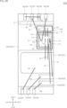
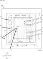
- FIG. 3 is a partially enlarged view of FIG. 2.
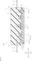
- FIG. 4 is a cross-sectional view taken along line IV-IV in FIG. 2.
- FIG. 5 is a cross-sectional view taken along line V-V in FIG. 2.
- the multiple connecting members 41 to 48 are omitted.
- FIG. 6 is a cross-sectional view taken along line VI-VI in FIG. 3.
- FIG. 7 is a cross-sectional view taken along line VII-VII in FIG. 3.
- FIG. 8 is a perspective view showing the state in which the driving device 7 is attached to the semiconductor device A10.
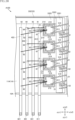
- FIG. 9 is a circuit diagram showing an example of the circuit configuration of the semiconductor device A10.
- the shape of the portion of the semiconductor device A10 covered by the resin member 5 when viewed in the thickness direction may be rectangular.
- the thickness direction of the semiconductor device A10 is defined as the z direction, and one direction perpendicular to the z direction is defined as the x direction.
- the x direction is, for example, the direction in which the power terminals 31, 32 of the semiconductor device A10 protrude, and may correspond to the left-right direction in Figure 2.
- the direction perpendicular to both the z direction and the x direction is defined as the y direction.
- the y direction may correspond to the up-down direction in Figure 2, for example. There are no particular limitations on the dimensions of the semiconductor device A10.
- the multiple semiconductor elements 11 may be elements that perform the electrical functions of the semiconductor device A10.
- Each semiconductor element 11 may be configured using a semiconductor material mainly made of, for example, SiC (silicon carbide).
- the semiconductor material is not limited to SiC, and may be Si (silicon), GaAs (gallium arsenide), GaN (gallium nitride), etc.
- Each semiconductor element 11 may be a switching element such as a metal-oxide-semiconductor field-effect transistor (MOSFET).
- MOSFET metal-oxide-semiconductor field-effect transistor
- Each semiconductor element 11 is not limited to a MOSFET, and may be a field-effect transistor including a metal-insulator-semiconductor FET (MISFET), or a bipolar transistor such as an insulated gate bipolar transistor (IGBT).
- the multiple semiconductor elements 11 may each be an n-channel MOSFET, and may all be the same type of element, but the present disclosure is not limited to this
- the multiple semiconductor elements 11 can be arranged at equal intervals in the x direction and connected in parallel to each other.
- the semiconductor device A10 can include three semiconductor elements 11.
- the number of semiconductor elements 11 is not limited to this and can be freely set according to the performance required of the semiconductor device A10.
- Each semiconductor element 11 can be bonded onto the support member 2 by a conductive bonding material 110.
- the conductive bonding material 110 can be, for example, solder, silver paste, or sintered metal.
- Each semiconductor element 11 may have an element principal surface 11a and an element rear surface 11b.
- the element principal surface 11a and the element rear surface 11b may face opposite each other in the z direction.
- the element principal surface 11a may face the z2 side in the z direction.
- the element rear surface 11b may face the z1 side in the z direction.
- the element rear surface 11b may face the support member 2.
- Each semiconductor element 11 may have a first electrode 111, a second electrode 112, and a third electrode 113.
- the first electrode 111 and the second electrode 112 may be arranged on the element main surface 11a.
- the first electrode 111 may be larger than the second electrode 112 in a planar view.
- the third electrode 113 may be arranged on the element back surface 12b.
- the third electrode 113 may cover the entire surface (or almost the entire surface) of the element back surface 11b.
- the constituent materials of the first electrode 111, the second electrode 112, and the third electrode 113 are not limited, but may be Al in this embodiment.
- the first electrode 111 may be a source electrode
- the second electrode 112 may be a gate electrode
- the third electrode 113 may be a drain electrode.
- the third electrode 113 may be conductively joined to a part of the support member 2 (the conductor layer 223 of the main surface metal layer 22 described later) via a conductive bonding material 110.
- the third electrode 113 can be configured to be in contact with the conductive bonding material 110.
- a metal plate 19 may be bonded to the first electrode 111 of each semiconductor element 11.
- the metal plate 19 may be arranged so as to be electrically connected to the first electrode 111 and to properly transfer heat from the semiconductor element 11.
- the connection members 41, 44 to 47 may be bonded to the metal plate 19.
- the metal plate 19 includes a third metal.
- the third metal may be Cu.
- the metal plate 19 may be, for example, a clad material in which a thin plate member made of Al is bonded to one surface of a plate member made of Cu.
- the metal plate 19 may be bonded to the first electrode 111 by, for example, solid-phase diffusion bonding, with the Al surface facing the first electrode 111 (Al).
- the configuration of the metal plate 19 and the method of bonding to the first electrode 111 are not limited.
- the metal plate 19 may be formed by forming an Al layer by sputtering or the like on one surface of a plate member made of Cu.
- the multiple semiconductor elements 12 can be, for example, diodes such as Schottky barrier diodes. Each semiconductor element 12 can be connected in inverse parallel to each semiconductor element 11, as shown in FIG. 9.
- Each semiconductor element 12 can be bonded onto the support member 2 by a conductive bonding material 120.
- the conductive bonding material 120 can be, for example, solder, silver paste, or sintered metal.
- the number of semiconductor elements 12 can correspond to the number of semiconductor elements 11. As an example, the semiconductor device A10 does not need to include each semiconductor element 12.
- Each semiconductor element 12 may have an element principal surface 12a and an element rear surface 12b.
- the element principal surface 12a and the element rear surface 12b may face opposite each other in the z direction.
- the element principal surface 12a may face the z2 side in the z direction.
- the element rear surface 12b may face the z1 side in the z direction.
- the element rear surface 12b may face the support member 2.
- Each semiconductor element 12 may have an anode electrode 121 and a cathode electrode 122.
- the anode electrode 121 may be disposed on the element's main surface 12a.
- the cathode electrode 122 may be disposed on the element's back surface 12b.
- the cathode electrode 122 may be electrically connected to a part of the support member 2 (the conductor layer 223 of the main surface metal layer 22 described below) via the conductive bonding material 120.
- the cathode electrode 122 may be in contact with the conductive bonding material 120.
- the support member 2 is a member that supports the multiple semiconductor elements 11, 12, and can provide a conductive path between each semiconductor element 11 and the multiple terminals 3.
- the support member 2 can include an insulating substrate 21, a main surface metal layer 22, and a back surface metal layer 23.
- the insulating substrate 21 may be, for example , flat and electrically insulating.
- the constituent material of the insulating substrate 21 may be, for example, ceramics with excellent thermal conductivity, and in this embodiment, may be Al2O3 (aluminum oxide).
- the constituent material of the insulating substrate 21 is not limited, and may be other ceramics such as AlN (aluminum nitride) and SiN (silicon nitride).
- the constituent material of the insulating substrate 21 is not limited to ceramics, and may be Si or synthetic resin.
- the constituent material of the insulating substrate 21 may be any material that is insulating and can withstand the heat generated by the semiconductor element 11.
- the insulating substrate 21 may have a principal surface 211 and a rear surface 212.
- the principal surface 211 and the rear surface 212 may face opposite sides to each other in the z direction.
- the principal surface 211 may face the z2 side in the z direction.
- the rear surface 212 may face the z1 side in the z direction.
- the principal surface metal layer 22 may be formed on the principal surface 211 of the insulating substrate 21.
- the constituent material of the principal surface metal layer 22 may be, for example, a metal containing Cu.
- the constituent material of the principal surface metal layer 22 is not limited.
- the principal surface metal layer 22 may be formed, for example, by plating.
- the method of forming the principal surface metal layer 22 is not limited.
- the principal surface metal layer 22 may be covered with a resin member 5.
- the principal surface metal layer 22 may include conductor layers 221 to 225 and a plurality of conductor layers 226 to 229.
- the conductor layers 221 to 229 may be arranged spaced apart from each other.
- the conductive layer 221 may include a strip portion 221a and a terminal joint portion 221b.
- the strip portion 221a extends along the x direction, and a plurality of connection members 41 and connection members 42 may be joined to the strip portion 221a.
- the terminal joint portion 221b is connected to the end portion of the strip portion 221a on the x2 side in the x direction, and a part of the power terminal 32 (pad portion 321 described below) may be joined to the terminal joint portion 221b.
- the conductive layer 222 may include a strip portion 222a and a terminal joint portion 222b.
- the strip portion 222a extends along the x direction, and a plurality of connection members 43 may be joined to each of them.
- the terminal joint portion 222b is connected to the end portion of the strip portion 222a on the x1 side in the x direction, and a part of the signal terminal 33 (a pad portion 331 described below) may be joined to the terminal joint portion 222b.
- the conductive layer 223 may include a strip portion 223a and a terminal joint portion 223b.
- the strip portion 223a extends along the x direction, and multiple semiconductor elements 11, 12 may be joined to the strip portion 223a. Heat from each semiconductor element 11 may be appropriately transferred to the strip portion 223a (conductive layer 223) via the conductive bonding material 110.
- the multiple semiconductor elements 11 joined to the strip portion 223a may be arranged in the direction in which the strip portion 223a extends (x direction).
- the terminal joint portion 223b is connected to the end portion of the strip portion 223a on the x direction x1 side, and a part of the power terminal 31 (pad portion 311 described below) may be joined to the strip portion 223a. As shown in FIGS.
- the conductor layer 223 can be electrically connected to the third electrode 113 (drain electrode) of each semiconductor element 11 via each conductive bonding material 110, and can be electrically connected to the cathode electrode 122 of each semiconductor element 12 via each conductive bonding material 120.
- the third electrode 113 of each semiconductor element 11 and the cathode electrode 122 of each semiconductor element 12 can be electrically connected to each other via the conductor layer 223.
- the conductive layer 224 may include a strip portion 224a and a terminal joint portion 224b.
- the strip portion 224a extends along the x direction, and a plurality of connection members 44 may be joined to each of them.
- the terminal joint portion 224b is connected to the end of the strip portion 224a on the x1 side in the x direction, and a part of the detection terminal 35 (pad portion 351 described below) may be joined to the terminal joint portion 224b.
- the conductive layer 225 can be joined to the connection member 42.
- the conductive layer 225 can be joined to a portion of the detection terminal 34 (the pad portion 341 described below).
- the multiple strip portions 221a, 222a, 223a, and 224a are arranged in the y direction and may overlap each other when viewed in the y direction.
- the arrangement of the multiple strip portions 221a, 222a, 223a, and 224a in the y direction is not particularly limited. In this embodiment, as shown in Figures 2 and 3, the strip portions 224a, 222a, 221a, and 223a may be arranged in this order from the y direction y1 side to the y direction y2 side.
- the strip portion 221a may be arranged between the strip portions 222a and 223a in the y direction, and the strip portion 222a may be arranged between the strip portions 221a and 224a in the y direction.
- the strip portion 223a may be arranged on the opposite side of the strip portion 222a in the y direction, sandwiching the strip portion 221a therebetween.
- the conductive layer 225 can be disposed on the x1 side of the terminal joint portion 222b of the conductive layer 222 in the x direction.
- the multiple conductor layers 226, 227 may all be arranged on the y2 side of the strip portion 223a of the conductor layer 223.
- the main surface metal layer 22 may include the same number of conductor layers 226 and conductor layers 227 as the semiconductor elements 11 (three in this embodiment).
- a connection member 46 may be joined to each conductor layer 226.
- a part of the temperature detection terminal 36 (pad portion 361 described below) may be joined to each conductor layer 226.
- a connection member 47 may be joined to each conductor layer 227.
- a part of the temperature detection terminal 37 (pad portion 371 described below) may be joined to each conductor layer 227.
- a temperature sensor 15 may be arranged on each conductor layer 227.
- the plurality of conductor layers 228, 229 may all be disposed on the y2 side of the strip portion 223a of the conductor layer 223 in the y direction.
- the main surface metal layer 22 may include the same number of conductor layers 228 and conductor layers 229 as the semiconductor elements 11 (three in this embodiment).
- Each conductor layer 228 may be joined to a connection member 48.
- Each conductor layer 228 may be joined to a part of the temperature detection terminal 38 (pad portion 381 described below).
- Each conductor layer 229 may be joined to a connection member 48.
- Each conductor layer 229 may be joined to a part of the temperature detection terminal 39 (pad portion 391 described below).
- Each conductor layer 226 to 229 may be arranged in a line along the x direction.
- Three groups of conductor layers 226 to 229 may be arranged along the x direction, in which the conductor layers 226 to 229 are arranged in this order from the x2 side to the x1 side in the x direction
- each conductive layer 221-229 are not limited to those described above, and can be designed appropriately depending on the arrangement position of each terminal 3, etc.
- the back metal layer 23 may be formed on the back surface 212 of the insulating substrate 21.
- the constituent material of the back metal layer 23 may be, for example, a metal containing Cu. The constituent material is not limited.
- the back metal layer 23 may be formed, for example, by electroless plating.
- the method of forming the back metal layer 23 is not limited. As shown in Figures 4 and 5, the surface of the back metal layer 23 facing the z-direction z1 side may be exposed from the resin member 5. The surface facing the z-direction z1 side may be covered by the resin member 5.
- the support member 2 may not include the back metal layer 23. In this case, the back surface 212 of the insulating substrate 21 may be covered by the resin member 5 or may be exposed from the resin member 5.
- the support member 2 can be formed using a DBC (Direct Bonding Copper) substrate in which Cu foil is bonded to the main surface 211 and the back surface 212 of the insulating substrate 21.
- DBC Direct Bonding Copper
- the Cu foil bonded to the main surface 211 can be patterned to form the main surface metal layer 22.
- the Cu foil bonded to the back surface 212 can become the back surface metal layer 23.
- Each terminal 3 may be joined to the main surface metal layer 22 inside the resin member 5. Each terminal 3 may protrude from the insulating substrate 21 when viewed in the z direction. A portion of each terminal 3 may be exposed from the resin member 5. Each terminal 3 may be made of the same lead frame, for example. Each terminal 3 may be made of a metal. As an example, each terminal 3 may be made of either Cu or Ni, or an alloy of these, 42 alloy, etc.
- the power terminal 31 may be a drain terminal in the semiconductor device A10.
- the power terminal 31 may be a plate-shaped member.
- the power terminal 31 may be electrically connected to the third electrode 113 (drain electrode) of each semiconductor element 11 via the conductive layer 223 and the conductive bonding material 110.
- the power terminal 31 may include a pad portion 311 and a terminal portion 312.
- the pad portion 311 may be covered with a resin member 5.
- the pad portion 311 may be bonded to the conductive layer 223. This bonding may be performed by any method, such as bonding using a conductive bonding material (such as solder, silver paste, or sintered metal), laser bonding, or ultrasonic bonding.
- the terminal portion 312 may be exposed from the resin member 5. As shown in FIG. 2, the terminal portion 312 may extend from the resin member 5 to the x1 side in the x direction when viewed in the z direction.
- the surface of the terminal portion 312 may be silver plated, for example.
- the power terminal 32 may be a source terminal in the semiconductor device A10.
- the power terminal 32 may be a plate-shaped member.
- the power terminal 32 may be electrically connected to the first electrode 111 (source electrode) of each semiconductor element 11 via the conductive layer 221, the multiple connection members 41, and the metal plate 19.
- the power terminal 32 may include a pad portion 321 and a terminal portion 322.
- the pad portion 321 may be covered with a resin member 5.
- the pad portion 321 may be bonded to the conductive layer 221. This bonding may be by any method, such as bonding using a conductive bonding material, laser bonding, or ultrasonic bonding.
- the terminal portion 322 may be exposed from the resin member 5. As shown in FIG. 2, the terminal portion 322 may extend from the resin member 5 to the x2 side in the x direction when viewed in the z direction.
- the surface of the terminal portion 322 may be silver plated, for example.
- the signal terminal 33 may be a gate terminal in the semiconductor device A10.
- the signal terminal 33 may be electrically connected to the second electrode 112 (gate electrode) of each semiconductor element 11 via the conductive layer 222 and the multiple connection members 43.
- a drive signal for controlling the on/off of each semiconductor element 11 may be input to the signal terminal 33.
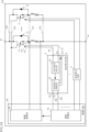
- a drive circuit DR may be connected to the signal terminal 33.
- the drive circuit DR may generate a drive signal that controls the switching operation of each semiconductor element 11.
- a drive signal may be input from the drive circuit DR to the signal terminal 33.
- the drive circuit DR shown in FIG. 9 is just an example, and is not limited to the circuit configuration shown.
- the signal terminal 33 may include a pad portion 331 and a terminal portion 332.
- the pad portion 331 may be covered with a resin member 5.
- the pad portion 331 may be bonded to the conductive layer 222. This bonding may be performed by any method, such as bonding using a conductive bonding material, laser bonding, or ultrasonic bonding.
- the terminal portion 332 may be exposed from the resin member 5.
- the terminal portion 332 may be L-shaped when viewed in the x-direction.
- the detection terminal 34 may be a source sense terminal in the semiconductor device A10.
- the detection terminal 34 may be electrically connected to the first electrode 111 (source electrode) of the semiconductor element 11 via the conductive layer 225, the connection member 42, the conductive layer 221, the multiple connection members 41, and the metal plate 19.
- the drive circuit DR may be connected to the detection terminal 34.
- the voltage applied to the detection terminal 34 may be input to the drive circuit DR as a feedback signal.
- the detection terminal 34 may include a pad portion 341 and a terminal portion 342.
- the pad portion 341 may be covered with a resin member 5.
- the pad portion 341 may be bonded to the conductive layer 225. This bonding may be performed by any method, such as bonding using a conductive bonding material, laser bonding, or ultrasonic bonding.
- the terminal portion 342 may be exposed from the resin member 5.
- the terminal portion 342 may be L-shaped when viewed in the x-direction.
- the detection terminal 35 may be a source sense terminal in the semiconductor device A10.
- the detection terminal 35 may be electrically connected to the first electrode 111 (source electrode) of each semiconductor element 11 via the conductive layer 224, the multiple connection members 44, and the metal plate 19.
- a Miller clamp circuit MC outside the semiconductor device A10 may be connected between the detection terminal 35 and the signal terminal 33.
- the Miller clamp circuit MC is a circuit for preventing malfunction (false gate on) of each semiconductor element 11, and may include, for example, a MOSFET as shown in FIG. 9.
- the source terminal of the MOSFET may be connected to the detection terminal 35, and the drain terminal of the MOSFET may be connected to the signal terminal 33.
- turning on the MOSFET of the Miller clamp circuit MC may force the gate-source voltage of the semiconductor element 11 to approximately 0 (zero) V or a negative bias voltage, thereby preventing the gate potential of the semiconductor element 11 from rising.
- the detection terminal 35 may include a pad portion 351 and a terminal portion 352.
- the pad portion 351 may be covered with a resin member 5.
- the pad portion 351 may be bonded to the conductive layer 224. This bonding may be performed by any method, such as bonding using a conductive bonding material, laser bonding, or ultrasonic bonding.
- the terminal portion 352 may be exposed from the resin member 5.
- the terminal portion 352 may be L-shaped when viewed in the x-direction, as shown in FIG. 4.
- the detection terminal 34, the signal terminal 33, and the detection terminal 35 are arranged in this order along the x direction from the x1 side to the x2 side in the x direction as shown in Figures 2 and 3, and may overlap when viewed in the x direction as shown in Figure 4.
- the detection terminal 34, the signal terminal 33, and the detection terminal 35 may protrude from the resin side surface 533 on the y1 side in the y direction.
- the multiple temperature detection terminals 36, 37 may each be a terminal for detecting the temperature of the semiconductor element 11.
- One corresponding temperature detection terminal 36 and one corresponding temperature detection terminal 37 may be provided for one semiconductor element 11.
- the semiconductor device A10 may include three semiconductor elements 11, and therefore may include three temperature detection terminals 36 and three temperature detection terminals 37.
- Each temperature detection terminal 36 may be bonded to the conductive layer 226.
- Each temperature detection terminal 36 may be electrically connected to the connection member 46 via the conductive layer 226.
- Each temperature detection terminal 37 may be bonded to the conductive layer 227.
- Each temperature detection terminal 37 may be electrically connected to the connection member 47 via the conductive layer 227.
- the temperature detection terminal 36 may include a pad portion 361 and a terminal portion 362.
- the pad portion 361 may be covered by the resin member 5.
- the pad portion 361 may be bonded to the conductive layer 226. This bonding may be any method such as bonding using a conductive bonding material, laser bonding, or ultrasonic bonding.
- the terminal portion 362 may be exposed from the resin member 5.
- the terminal portion 362 may be L-shaped when viewed in the x direction, as shown in FIG. 4.
- the temperature detection terminal 37 may include a pad portion 371 and a terminal portion 372.
- the pad portion 371 may be covered by the resin member 5.
- the pad portion 371 may be bonded to the conductive layer 227. This bonding may be any method such as bonding using a conductive bonding material, laser bonding, or ultrasonic bonding.
- the terminal portion 372 may be exposed from the resin member 5.
- the terminal portion 372 may be L-shaped when viewed in the x direction.
- the multiple temperature detection terminals 38, 39 may each be a terminal for outputting a detection signal from the temperature sensor 15.
- One corresponding temperature detection terminal 38 and one corresponding temperature detection terminal 39 may be provided for one temperature sensor 15.
- the semiconductor device A10 may include three temperature sensors 15, and therefore may include three temperature detection terminals 38 and three temperature detection terminals 39.
- Each temperature detection terminal 38 may be bonded to the conductive layer 228.
- Each temperature detection terminal 38 may be electrically connected to the temperature sensor 15 via the conductive layer 228 and the connection member 48.
- Each temperature detection terminal 39 may be bonded to the conductive layer 229.
- Each temperature detection terminal 39 may be electrically connected to the temperature sensor 15 via the conductive layer 229 and the connection member 48.
- the temperature detection terminal 38 may include a pad portion 381 and a terminal portion 382.
- the pad portion 381 may be covered by the resin member 5.
- the pad portion 381 may be bonded to the conductive layer 228. This bonding may be any method such as bonding using a conductive bonding material, laser bonding, or ultrasonic bonding.
- the terminal portion 382 may be exposed from the resin member 5.
- the terminal portion 382 may be L-shaped when viewed in the x direction.
- the temperature detection terminal 39 may include a pad portion 391 and a terminal portion 392.
- the pad portion 391 may be covered by the resin member 5.
- the pad portion 391 may be bonded to the conductive layer 229. This bonding may be any method such as bonding using a conductive bonding material, laser bonding, or ultrasonic bonding.
- the terminal portion 392 may be exposed from the resin member 5.
- the terminal portion 392 may be L-shaped when viewed in the x direction.
- the temperature detection terminals 36 to 39 are aligned along the x direction as shown in Figures 2 and 3, and may overlap when viewed in the x direction as shown in Figure 4. Each of the temperature detection terminals 36 to 39 may protrude from the resin side surface 534 on the y2 side in the y direction.
- Each of the multiple connection members 41-45, 48 can provide electrical continuity between two separated portions.
- Each of the connection members 41-45, 48 can be a bonding wire.
- each of the connection members 41-45, 48 can be formed by wedge bonding.
- Each of the connection members 41-45, 48 may be formed by ball bonding.
- the constituent material of each of the connection members 41-45, 48 is, for example, Al, Au, Cu, or an alloy containing any of these, but is not limited thereto. In this embodiment, as an example, a case will be described in which the constituent material of each of the connection members 41-45, 48 is Cu.
- Each of the multiple connection members 41 can have one end bonded to the metal plate 19 and the other end bonded to the conductive layer 221. Each connection member 41 can provide electrical continuity between the first electrode 111 (source electrode) of each semiconductor element 11 and the conductive layer 221.
- connection member 42 may have one end bonded to the conductive layer 221 and the other end bonded to the conductive layer 225.
- the connection member 42 may provide electrical continuity between the conductive layer 221 and the conductive layer 225.
- the other end of the connection member 42 may be bonded to the pad portion 341 of the detection terminal 34, rather than to the conductive layer 225.
- Each of the multiple connection members 43 can have one end bonded to the second electrode 112 (gate electrode) of each semiconductor element 11, and the other end bonded to the conductive layer 222.
- Each connection member 43 can provide electrical continuity between each second electrode 112 and the conductive layer 222.
- Each of the multiple connection members 44 can have one end bonded to the metal plate 19 and the other end bonded to the conductive layer 224. Each connection member 44 can electrically connect the first electrode 111 (source electrode) of each semiconductor element 11 to the conductive layer 224. Each connection member 44 can be a sense line Kelvin-connected to the first electrode 111 (source electrode) of each semiconductor element 11.
- Each of the multiple connection members 45 can have one end joined to the metal plate 19 and the other end joined to the anode electrode 121 of each semiconductor element 12.
- Each connection member 45 can electrically connect the first electrode 111 (source electrode) of each semiconductor element 11 to the anode electrode 121 of each semiconductor element 12.
- connection members 48 may either have one end joined to one electrode of the temperature sensor 15 and the other end joined to the conductive layer 228, or have one end joined to the other electrode of the temperature sensor 15 and the other end joined to the conductive layer 229.
- Each connection member 48 may provide electrical conductivity between each temperature sensor 15 and the conductive layer 228 or the conductive layer 229.
- Each of the multiple connection members 46, 47 may be a member for detecting the temperature of the semiconductor element 11.
- Each of the connection members 46, 47 may be formed by a bonding wire forming method, similar to the connection members 41 to 45, 48. In this embodiment, each of the connection members 46, 47 may be formed by wedge bonding.
- Each of the connection members 46, 47 may be formed by ball bonding.
- Each of the connection members 46 may have one end bonded to the metal plate 19 and the other end bonded to the conductive layer 226.
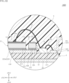
- Each of the connection members 47 may have a first end 47a and a second end 47b. The first end 47a is one end of the connection member 47 and may be bonded to the metal plate 19.
- connection members 46, 47 may be directly bonded to the metal plate 19.
- connection members 46, 47 and the metal plate 19 can be in direct contact with each other without any other member interposed therebetween. In the metal plate 19, the connection members 46 and 47 can be joined separately from each other.
- the material of the connection member 46 is a first metal.
- the first metal may be Cu, which is the same as the third metal.
- the material of the connection member 47 is a second metal whose thermoelectric power may differ from that of the first metal.
- Thermoelectric power refers to the thermoelectromotive force per 1 K when a temperature difference is applied to both ends of a conductive material.
- the second metal may be constantan (an alloy of Cu and Ni: 55Cu-45Ni).
- the connection member 46 and the metal plate 19 (Cu) and the connection member 47 (constantan) may function as a thermocouple.
- a thermocouple made of Cu and constantan is known as a T-type thermocouple.
- the junction 47c between the connection member 47 and the metal plate 19 may correspond to the temperature measuring junction (hot junction) of the thermocouple.
- the junction between the connection member 46 and the conductive layer 226 and the junction between the connection member 47 and the conductive layer 227 may correspond to the reference junction (cold junction) of the thermocouple.
- a voltage may be generated between the reference junctions.
- the temperature detection terminals 36 and 37 may output the voltage between the reference junctions to the drive device 7 as a signal for detecting the temperature of the semiconductor element 11.
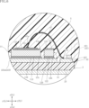
- the temperature sensor 15 can detect the temperature (hereinafter referred to as the "reference temperature") of the reference junction (cold junction) of the thermocouple.
- the temperature sensor 15 can be arranged at a position closer to the second end 47b of the connection member 47 than the semiconductor element 11.
- the temperature sensor 15 can be arranged on the conductive layer 227.
- the arrangement position and arrangement direction of the temperature sensor 15 on the conductive layer 227 are not limited, and can be appropriately designed so that the temperature sensor 15 is as close as possible to the second end 47b of the connection member 47 and the connection members 47, 48 are easily formed.
- an insulating layer 16 can be interposed between the temperature sensor 15 and the conductive layer 227.
- an element in which the temperature sensor 15 and the insulating layer 16 are integrated can be arranged on the conductive layer 227 with the insulating layer 16 facing the conductive layer 227.
- the temperature sensor 15 can be arranged on the insulating layer 16 arranged on the conductive layer 227.
- the temperature sensor 15 may be a temperature sensor that utilizes the temperature characteristics of a PN junction type Si diode.
- the temperature sensor 15 may be any sensor whose electrical signal changes depending on the surrounding temperature, and may be, for example, a thermistor.
- the temperature sensor 15 may output a detection signal of the reference temperature to the outside via the two connection members 48, the conductive layers 228 and 229, and the temperature detection terminals 38 and 39.
- the resin member 5 may be an electrically insulating semiconductor encapsulant.
- the resin member 5 may cover the entirety of the semiconductor elements 11, the semiconductor elements 12, the temperature sensors 15, the insulating substrate 21, the main surface metal layer 22, and the connection members 41-48, as well as a portion of each of the terminals 3.
- the material of the resin member 5 may be, for example, epoxy resin.
- the resin member 5 may be formed, for example, by transfer molding using a mold. There is no limitation on the method of forming the resin member 5.
- the resin member 5 may have a resin main surface 51, a resin back surface 52, and multiple resin side surfaces 531-534, as shown in Figures 2, 4, and 5.
- the resin main surface 51 and the resin back surface 52 may face opposite sides to each other in the z direction.
- the resin main surface 51 may face the z direction z2 side, and the resin back surface 52 may face the z direction z1 side.
- the back surface metal layer 23 may be exposed from the resin back surface 52.
- the resin back surface 52 and the surface of the back surface metal layer 23 facing the z direction z1 side may be flush with each other.
- Each of the multiple resin side surfaces 531 to 534 may be connected to both the resin main surface 51 and the resin back surface 52 and may be sandwiched between them. As shown in FIG. 2, the two resin side surfaces 531, 532 may face opposite sides to each other in the x direction.
- the resin side surface 531 may be a surface arranged on the x direction x1 side and facing the x direction x1 side.
- the resin side surface 532 may be a surface arranged on the x direction x2 side and facing the x direction x2 side.
- the two resin side surfaces 533, 534 may face opposite sides to each other in the y direction.
- the resin side surface 533 may be a surface disposed on the y-direction y1 side and facing the y-direction y1 side.
- the resin side surface 534 may be a surface disposed on the y-direction y2 side and facing the y-direction y2 side.
- the resin side surfaces 531 to 534 may each have a surface that is connected to the resin main surface 51 and inclined so as to approach each other toward the resin main surface 51.
- the portions of the resin member 5 that are connected to these inclined surfaces and surrounded by the resin main surface 51 may have a tapered shape in which the cross-sectional area in the xy plane decreases toward the resin main surface 51.
- the resin side surfaces 531 to 534 may each have a surface that is connected to the resin back surface 52 and inclined so as to approach each other toward the resin back surface 52.
- the portions of the resin member 5 that are connected to these inclined surfaces and surrounded by the resin main surface 51 may have a tapered shape in which the cross-sectional area in the xy plane decreases toward the resin back surface 52.
- the shapes of the resin member 5 shown in Figures 1 to 5 are examples. The shape of the resin member 5 is not limited to the exemplified shapes.
- the driving device 7 may be a device that drives the semiconductor device A10. As shown in FIG. 8, the driving device 7 may be attached to the z2 side of the semiconductor device A10 in the z direction. As shown in FIG. 8, the driving device 7 may include a substrate 71, terminals 723, 724, and 725, and a plurality of terminals 721, 722, 726, and 727.
- the substrate 71 may be, for example, flat and electrically insulating.
- the material of the substrate 71 is not limited.
- the substrate 71 may have a main surface 711 and a back surface 712. The main surface 211 and the back surface 712 may face opposite sides to each other in the z direction.
- the main surface 711 may face the z2 side in the z direction.
- the back surface 712 may face the z1 side in the z direction.
- Wiring may be formed on the main surface 711, and an external connector and a large number of electronic components may be mounted thereon. In FIG. 8, the wiring, external connector, electronic components, and the like on the main surface 711 are omitted.
- Each of the terminals 721-727 is a cylindrical metal member, and may be inserted into a through hole that penetrates the substrate 71 in the z-direction from the main surface 711 to the back surface 712. Each of the terminals 721-727 may be electrically connected to wiring formed on the main surface 711.
- the terminals 332, 342, 352, 362, 372, 382, and 392 of the terminals 33-39 of the semiconductor device A10 may be inserted into each of the terminals 721-727, and may be joined, for example, by solder.
- the signal terminal 33 may be joined to the terminal 723.
- the detection terminal 34 may be joined to the terminal 724.
- the detection terminal 35 may be joined to the terminal 725.
- each of the terminals 721 may be joined to the temperature detection terminal 36. Since the temperature detection terminal 36 is conductively connected to the connection member 46 via the conductive layer 226, the terminal 721 can be conductively connected to the connection member 46. There are three terminals 722, the same as the temperature detection terminals 37, and each terminal 722 can be joined to a temperature detection terminal 37. Since the temperature detection terminal 37 is conductively connected to the connection member 47 via the conductive layer 227, the terminal 722 can be conductively connected to the connection member 47.
- the terminals 726 are arranged in three numbers, the same as the temperature detection terminals 38, and each terminal 726 can be joined to a temperature detection terminal 38. Since the temperature detection terminals 38 are conductively connected to one electrode of the temperature sensor 15 via the conductive layer 228 and the connection member 48, the terminals 726 can be conductively connected to one electrode of the temperature sensor 15.
- the terminals 727 are arranged in three numbers, the same as the temperature detection terminals 39, and each terminal 727 can be joined to a temperature detection terminal 39. Since the temperature detection terminals 39 are conductively connected to the other electrode of the temperature sensor 15 via the conductive layer 229 and the connection member 48, the terminals 727 can be conductively connected to the other electrode of the temperature sensor 15.
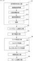
- the driving device 7 may include, as its functional configuration, a plurality of relative temperature detection units 73, a plurality of reference junction compensation units 74, an overheat protection unit 75, and a driving control unit 76.
- the driving control unit 76 is a functional configuration that controls the switching operation of each semiconductor element 11, and may be realized, for example, by a gate driving IC.
- the driving control unit 76 may include a drive circuit DR and a Miller clamp circuit MC.
- the driving control unit 76 may generate a driving signal based on a control signal input from the outside, and output the driving signal to the semiconductor device A10 via the terminal 723.
- the semiconductor device A10 may receive a driving signal from the signal terminal 33 connected to the terminal 723, and control the switching operation of each semiconductor element 11.
- the driving control unit 76 may receive a signal from the detection terminal 34 of the semiconductor device A10 via the terminal 724, and a signal from the detection terminal 35 via the terminal 725.
- the specific circuit configuration and mode of the driving control unit 76 are
- the relative temperature detection unit 73 and the reference junction compensation unit 74 may be functional components for detecting the temperature of the semiconductor element 11. Three of each of the relative temperature detection units 73 and the reference junction compensation units 74 may be provided in accordance with the number of semiconductor elements 11 of the semiconductor device A10. Each relative temperature detection unit 73 may receive a voltage from a pair of temperature detection terminals 36 and 37 of the semiconductor device A10 via a pair of terminals 721 and 722. The voltage may be a voltage between the reference junction of a thermocouple having the connection member 46 and the metal plate 19 and the connection member 47, and may be a voltage corresponding to the temperature difference between the reference junction and the temperature measurement junction. The voltage may be a voltage corresponding to the relative temperature of the semiconductor element 11 with respect to a reference temperature, which is the temperature of the reference junction. Each relative temperature detection unit 73 may detect the relative temperature of the corresponding semiconductor element 11 based on the input voltage.
- Each reference junction compensation unit 74 can convert the relative temperature detected by the corresponding relative temperature detection unit 73 into an absolute temperature.
- Each reference junction compensation unit 74 can receive a detection signal from the temperature sensor 15 via a pair of terminals 726, 727 from a pair of temperature detection terminals 38, 39 of the semiconductor device A10.
- the detection signal can be a signal detected by the temperature sensor 15 to detect the reference temperature of the corresponding thermocouple.
- the reference junction compensation unit 74 can detect the reference temperature of the corresponding thermocouple based on the input detection signal.
- the reference junction compensation unit 74 can convert the detected reference temperature into an absolute temperature by adding it to the relative temperature detected by the corresponding relative temperature detection unit 73.
- the reference junction compensation unit 74 can output the absolute temperature of the corresponding semiconductor element 11 to the overheat protection unit 75.
- the specific circuit configurations of the relative temperature detection unit 73 and the reference junction compensation unit 74 are not limited. For example, they may be configured as follows.
- the relative temperature detection unit 73 may transmit the voltage between the pair of terminals 721, 722 to the reference junction compensation unit 74 as a voltage corresponding to the relative temperature of the corresponding semiconductor element 11.
- the reference junction compensation unit 74 may then convert the voltage corresponding to the detected reference temperature into a voltage corresponding to the thermoelectromotive force of the thermocouple, add it to the voltage transmitted from the relative temperature detection unit 73, and output it to the overheat protection unit 75.
- a voltage corresponding to the absolute temperature of the semiconductor element 11 may be input to the overheat protection unit 75.
- the overheat protection unit 75 can detect an overheating abnormality of the corresponding semiconductor element 11 based on the absolute temperature input from each reference junction compensation unit 74.
- the overheat protection unit 75 can output an abnormality detection signal to the drive control unit 76 when the absolute temperature input from each reference junction compensation unit 74 becomes equal to or higher than a threshold temperature.
- the drive control unit 76 receives the abnormality detection signal, it can stop driving the semiconductor device A10 by stopping the output of the drive signal.
- the specific circuit configuration of the overheat protection unit 75 is not limited.
- the overheat protection unit 75 can include a comparator that generates an abnormality detection signal when a voltage corresponding to the absolute temperature input from the reference junction compensation unit 74 becomes equal to or higher than a voltage corresponding to the threshold temperature.
- the driving device 7 can be attached to the semiconductor device A10.
- the combined driving device 7 and semiconductor device A10 can be referred to as a semiconductor device as a whole.
- Figure 10 is a flowchart showing an example of a method for manufacturing the semiconductor device A10.
- Figures 11 to 17 are diagrams showing steps in an example of a method for manufacturing the semiconductor device A10.
- Figures 11 to 14 and Figures 16 to 17 are cross-sectional views, and correspond to Figure 4.
- Figure 15 is an enlarged plan view, and corresponds to Figure 3.
- the x, y, and z directions shown in Figures 11 to 17 indicate the same directions as Figures 1 to 8.
- the manufacturing method for semiconductor device A10 can include a support member forming process (S1), a lead frame joining process (S2), an element mounting process (S3), a wire forming process (S4), a resin forming process (S5), and a frame cutting process (S6).
- S1 support member forming process
- S2 lead frame joining process
- S3 element mounting process
- S4 wire forming process
- S5 resin forming process
- S6 frame cutting process
- the support member forming step (S1) may include a step of forming the support member 2.
- an insulating substrate 91 is prepared (S11).
- the insulating substrate 91 may be made of, for example, ceramics and may have a main surface 911 and a back surface 912 facing opposite sides in the z direction.
- a main surface metal layer 22 is formed on the main surface 911 of the insulating substrate 91 (S12).
- the main surface metal layer 22 may be formed, for example, by electroless plating or sputtering to form a base layer covering the entire main surface 911, forming a mask to form a plating layer by electrolytic plating, and removing unnecessary parts of the base layer by etching. As shown in FIG.
- a back surface metal layer 23 is formed on the back surface 912 of the insulating substrate 91 (S13).
- the back surface metal layer 23 may be formed, for example, by electroless plating.
- a DBC substrate having Cu foil bonded to the main surface 911 and the back surface 912 of the insulating substrate 91 may be used, and the Cu foil on the main surface 911 side may be patterned to form the main surface metal layer 22 and the back surface metal layer 23 on the insulating substrate 91.
- the insulating substrate 91 is cut (S14). By cutting the insulating substrate 91, the insulating substrate 21 can be formed. In this manner, the support member 2 can be formed.
- a lead frame 92 that will become each terminal 3 is prepared.
- the lead frame 92 may have a portion that will become each terminal 3, and a frame to which the multiple terminals 3 are connected. There are no limitations on the shape of the lead frame 92, etc.
- a conductive bonding paste is placed at the position where each terminal 3 is to be bonded to the main surface metal layer 22, and as shown in FIG. 13, the portion of the lead frame 92 that will become each terminal 3 is bonded to the main surface metal layer 22.
- the portion of the lead frame 92 that will become the detection terminal 35 may be bonded to the conductive layer 224.
- the portion of the lead frame 92 that will become the temperature detection terminal 36 may be bonded to the conductive layer 226. There are no limitations on the method of bonding the lead frame 92.
- a conductive bonding paste 93 is placed in the area of the conductive layer 223 where the semiconductor elements 11 and 12 are to be placed.
- the conductive bonding paste 93 can be, for example, solder, silver paste, or sintered metal.
- a plurality of semiconductor elements 11 and a plurality of semiconductor elements 12 are attached to the conductive bonding paste 93, heated, and then cooled.
- the conductive bonding paste 93 interposed between the conductive layer 223 and the semiconductor element 11 becomes the conductive bonding material 110, and the semiconductor element 11 can be bonded to the conductive layer 223 via the conductive bonding material 110.
- the semiconductor element 11 can have a metal plate 19 bonded to the first electrode 111 in advance.
- the conductive bonding paste 93 interposed between the conductive layer 223 and the semiconductor element 12 becomes the conductive bonding material 120, and the semiconductor element 12 can be bonded to the conductive layer 223 via the conductive bonding material 120.
- an element in which the temperature sensor 15 and insulating layer 16 are integrated is bonded onto the conductive layer 227 with the insulating layer 16 facing the conductive layer 227.
- the insulating layer 16 may be bonded onto the conductive layer 227, and the temperature sensor 15 may be bonded onto the insulating layer 16.
- Figure 14 shows the temperature sensor 15 disposed on the conductive layer 227 located on the x1 side of the conductive layer 226 in the x direction.
- connection members 41 to 48 are formed. As shown in FIG. 16, the connection members 41 to 46, 48 are formed by wedge bonding (S41).
- the connection member 41 may be formed to connect the metal plate 19 bonded to the first electrode 111 of the semiconductor element 11 to the conductive layer 221.
- the connection member 43 may be formed to connect the second electrode 112 of the semiconductor element 11 to the conductive layer 222.
- the connection member 44 may be formed to connect the metal plate 19 to the conductive layer 224.
- the connection member 45 may be formed to connect the metal plate 19 to the anode electrode 121 of the semiconductor element 12.
- the connection member 46 may be formed to connect the metal plate 19 to the conductive layer 226.
- connection member 48 may be formed to connect the temperature sensor 15 to the conductive layer 228 or the conductive layer 229.
- the connection member 42 may be formed to connect the conductive layer 221 and the conductive layer 225.
- the connection member 46 may be formed in the same process as the connection members 41 to 45 and 48, since the constituent material of the connection member 46 is Cu, which is the same as the connection members 41 to 45 and 48.
- the order of forming the connection members 41 to 46 and 48 is not limited.
- the connection member 47 is formed by wedge bonding (S42).
- the connection member 47 may be formed to connect the metal plate 19 and the conductive layer 227.
- connection member 47 may be formed in a process different from the connection members 41 to 46 and 48, since the constituent material of the connection member 47 is different from the connection members 41 to 46 and 48.
- the connection member 47 may be formed by the same equipment and method as the connection members 41 to 46 and 48, except that the material of the wire used is different.
- the connection member 47 may be formed before the connection members 41 to 46 and 48 are formed. In the wire forming process (S4), the connection members 46 and 47 are joined to the metal plate 19 to form a thermocouple.
- a part of the lead frame 92, a part of the support member 2, the plurality of semiconductor elements 11, 12, the temperature sensor 15, the conductor layer 228, and the plurality of connection members 41 to 48 are enclosed in a mold.
- a liquid resin material is injected into the space defined by the mold. The resin material is hardened to obtain the resin member 5.
- the lead frame 92 is cut at appropriate locations of the portions exposed from the resin member 5. This allows each terminal 3 to be separated from the others. Thereafter, each terminal 3 can be bent or otherwise processed as necessary to obtain the semiconductor device A10 described above.
- the metal plate 19 is joined to the first electrode 111 of each semiconductor element 11, and one end of each of the connection members 46 and 47 can be joined to the metal plate 19.
- the material of the connection member 46 is a first metal, which can be the same metal as the third metal that is the material of the metal plate 19.
- the material of the connection member 47 can be a second metal having a different thermoelectric power from the first metal.
- the connection member 46, the metal plate 19, and the connection member 47 function as a thermocouple, and the junction 47c between the connection member 47 and the metal plate 19 can be used as a thermocouple temperature measuring junction to detect temperature.
- the junction 47c can be in contact with the metal plate 19 to which heat from the semiconductor element 11 is appropriately transferred.
- the semiconductor device A10 can detect the temperature of each semiconductor element 11 with higher accuracy than when a temperature sensor is disposed near the semiconductor element 11.
- the semiconductor device A10 can improve the accuracy of the detected temperature of each semiconductor element 11 without forming a temperature sensor inside each semiconductor element 11.
- the first metal and the third metal can be Cu, and the second metal can be constantan. Therefore, the connection member 46 and the metal plate 19 (Cu) and the connection member 47 (constantan) can function as a T-type thermocouple.
- connection members 46 and 47 can be formed by the same bonding wire formation method as the connection members 41 to 45. Therefore, the connection members 46 and 47 can be formed by the same method using the same equipment as the connection members 41 to 45.
- the connection member 46 is made of the same Cu material as the connection members 41 to 45, and therefore can be formed in the same process as the connection members 41 to 45.
- a metal plate 19 can be bonded to the first electrode 111 of each semiconductor element 11. This can protect the semiconductor element 11 from impacts that occur when wedge bonding the connection members 41, 44 to 47.
- the drive device 7 can include a relative temperature detection unit 73 and a reference junction compensation unit 74. Therefore, the drive device 7 can convert the relative temperatures of each semiconductor element 11 detected by the thermocouple formed by the connection member 46 and the metal plate 19 and the connection member 47 into absolute temperatures, and use them for overheating protection.
- the temperature sensor 15 can be disposed in the semiconductor device A10 at a position close to the second end 47b of the connection member 47. Therefore, the temperature sensor 15 can detect the reference temperature more accurately than when the temperature sensor 15 is disposed in the drive device 7. According to this embodiment, the temperature sensor 15 can be disposed on the conductive layer 227 to which the second end 47b of the connection member 47 is bonded. Therefore, the temperature sensor 15 can detect the reference temperature more accurately than when the temperature sensor 15 is disposed in a position other than the conductive layer 227. According to this embodiment, the drive device 7 including the reference junction compensation unit 74 can be attached to the outside of the semiconductor device A10.
- the semiconductor device A10 has the temperature sensor 15 for detecting the reference temperature disposed inside and the drive device 7 attached outside, so that the detection error of the reference temperature can be reduced.
- the first metal which is the constituent material of the connection member 46
- the second metal which is the constituent material of the connection member 47
- the first metal and the second metal may be metals with different thermoelectric powers.
- the first metal may be Cu
- the second metal may be Al
- Cu and Al have the same polarity of thermoelectric power, but the absolute values of the thermoelectric power are different, so the connection member 46 and the metal plate 19 (Cu) and the connection member 47 (Al) can function as a thermocouple.
- Al is a common bonding wire, and is easily and inexpensively available compared to constantan wire.
- the combination of the first metal and the second metal may be Chromel (registered trademark) (90Ni-10Cr) and Alumel (registered trademark) (94Ni-3Al-1Si-2Mg) as in a K-type thermocouple, Fe and constantan as in a J-type thermocouple, or chromel and constantan as in an E-type thermocouple.
- Chromel registered trademark
- Alumel registered trademark
- 94Ni-3Al-1Si-2Mg chromel and constantan as in an E-type thermocouple.
- the combination of the first metal and the second metal is not limited to those described above.
- the first metal, which is the constituent material of the connection member 46, and the third metal, which is the constituent material of the metal plate 19, are the same metal (Cu), but this is not limited to the above.
- the first metal and the third metal may be different metals. In this case, it may be necessary to correct the difference between the detected temperature and the actual temperature. To improve the accuracy of the detected temperature, the third metal may be the same metal as the first metal (or the second metal).
- the temperature sensor 15 is disposed on the conductive layer 227, but this is not limiting.
- the temperature sensor 15 may be disposed on the conductive layer 228.
- the connection member 46 may be joined to the conductive layer 227, and the connection member 47 may be joined to the conductive layer 226. In these cases, the temperature sensor 15 may detect the temperature of the reference junction (cold junction) on the connection member 46 side. If the connection member 46 is Cu and the connection member 47 is constantan, a voltage difference may occur between both ends of the connection member 47. To detect the temperature of the second end 47b of the connection member 47, the temperature sensor 15 may be disposed on the conductive layer 227.
- connection members 41 to 47 are all bonding wires, but this is not limited to the above.
- Any of the connection members 41 to 47 may be a connection member other than a bonding wire (for example, a metal ribbon or a connection lead formed by bending a metal plate).
- a connection lead may be used that is joined to the anode electrode 121 of the semiconductor element 12, the first electrode 111 of the semiconductor element 11, and the conductive layer 221 to provide electrical conductivity between them.
- any of the multiple terminals 3 may be bonded to the insulating substrate 21 at a distance from the main surface metal layer 22.
- the terminal 3 can be conductively connected to the main surface metal layer 22 by a connecting member such as a bonding wire.
- FIGS. 18 to 20 show modified examples of the semiconductor device A10 according to the first embodiment.
- elements that are the same as or similar to those in the above embodiment are given the same reference numerals as in the above embodiment, and duplicated descriptions are omitted.
- Fig. 18 is a diagram for explaining a semiconductor device A11 according to a first modified example of the first embodiment.
- Fig. 18 is a partially enlarged plan view of the semiconductor device A11, and corresponds to Fig. 3.
- the resin member 5 is shown through for ease of understanding.
- the semiconductor device A11 may differ from the semiconductor device A10 in that the positions of the conductor layer 227 and the temperature detection terminal 37 and the conductor layer 228 and the temperature detection terminal 38 are interchanged.
- the conductive layer 227 to which the connection member 47 is joined may be disposed between the conductive layer 228 and the conductive layer 229. Accordingly, the temperature detection terminal 37 may be disposed between the temperature detection terminal 38 and the temperature detection terminal 39.
- the position and orientation of the temperature sensor 15 on the conductive layer 227 are not limited, and may be appropriately designed so that the temperature sensor 15 is as close as possible to the second end 47b of the connection member 47 and so that the connection members 47, 48 are easily formed.
- Fig. 19 is a diagram for explaining a semiconductor device A12 according to a second modified example of the first embodiment.
- Fig. 19 is a partially enlarged plan view of the semiconductor device A12, and corresponds to Fig. 3.
- the resin member 5 is shown through for ease of understanding.
- the semiconductor device A12 may differ from the semiconductor device A10 in that the connection member 47 is joined to the connection member 46 in the metal plate 19.
- connection member 47 can be joined to the connection member 46 which is joined to the metal plate 19. That is, the contact 47c of the connection member 47, which corresponds to the temperature measuring contact of the thermocouple, can be in direct contact with the connection member 46.
- the degree of freedom in selecting the constituent material of the connection member 46 and the connection member 47 can be increased.
- Fig. 20 is a diagram for explaining a semiconductor device A13 according to a third modified example of the first embodiment.
- Fig. 20 is a partially enlarged plan view of the semiconductor device A13, and corresponds to Fig. 3.
- the resin member 5 is shown through for ease of understanding.
- the semiconductor device A13 may differ from the semiconductor device A10 in that it does not include a metal plate 19.
- the metal plate 19 is not joined to the first electrode 111 of each semiconductor element 11 in this modified example.
- the connection members 41, 44 to 47 can be joined to the first electrode 111. Heat generated from the semiconductor element 11 can be transferred to the first electrode 111.
- the first electrode 111 is made of Al, so the second metal, which is the material of the connection member 47, can be Al.
- the contact 46c between the connection member 46 (Cu) and the first electrode 111 (Al) can correspond to the temperature measurement contact of the thermocouple.
- the material of the connection member 47 is not limited.
- the material of the first electrode 111 may be the same as the material of the connection member 46.
- the temperature measurement contact (contact 46c) can be in direct contact with the first electrode 111. Compared to the case where the temperature measurement contact is in contact with the metal plate 19, the accuracy of the detected temperature of each semiconductor element 11 can be improved in this modified example.
- Fig. 21 is a diagram for explaining a semiconductor device A14 according to a fourth modified example of the first embodiment.
- Fig. 21 is a partially enlarged plan view of the semiconductor device A14, and corresponds to Fig. 3.
- the resin member 5 is shown through for ease of understanding.
- the semiconductor device A14 may differ from the semiconductor device A10 in that the connection members 46, 47 are bonded to the main surface metal layer 22.
- connection members 46 and 47 can be joined to the main surface metal layer 22, not to the metal plate 19. More specifically, one end of the connection member 46 and one end of the connection member 47 (first end 47a) can be joined to the strip portion 223a of the conductive layer 223 at a position adjacent to the semiconductor element 11.
- the material of the strip portion 223a can be the same metal as the material of the connection member 46. Therefore, the connection member 46, the strip portion 223a, and the connection member 47 function as a thermocouple, and the junction 47c between the connection member 47 and the strip portion 223a can be used as a temperature measuring junction of the thermocouple to detect temperature.
- the semiconductor element 11 can be joined to the strip portion 223a, heat from the semiconductor element 11 can be appropriately transferred to the strip portion 223a via the conductive bonding material 110. Therefore, the temperature of the semiconductor element 11 can be detected by detecting the temperature at a position of the strip portion 223a adjacent to the semiconductor element 11.
- the arrangement of the conductive layers 226-229 and the terminals 36-39 differs from that of the semiconductor device A10, but the arrangement is not limited thereto. This modification can be effective in cases where the first electrode 111 of the semiconductor element 11 is small and it is difficult to join the connecting members 46, 47 to the metal plate 19.
- the parts of the first to fourth modified examples may be combined in any manner.
- FIGS. 22 to 36 show other embodiments of the present disclosure.
- elements that are the same as or similar to those in the above embodiment are given the same reference numerals as in the above embodiment, and duplicated descriptions are omitted.
- FIG. 22 and 23 are diagrams for explaining the semiconductor device A20 according to the second embodiment of the present disclosure.
- FIG. 22 is a cross-sectional view showing the semiconductor device A20, and corresponds to FIG. 4.
- FIG. 23 is a partially enlarged plan view showing the semiconductor device A20, and corresponds to FIG. 3.
- the outer shape of the resin member 5 is shown by an imaginary line (two-dot chain line) through the resin member 5.
- the semiconductor device A20 according to this embodiment may differ from the semiconductor device A10 according to the first embodiment in that the temperature sensor 15 is disposed on the temperature detection terminal 37.
- the configuration and operation of the other parts of this embodiment may be similar to those of the first embodiment.
- the parts of the first embodiment and each modification may be combined arbitrarily.
- each terminal 3 may be unbonded to the support member 2.
- the pad portion 351 of the detection terminal 35 may be unbonded to the main surface metal layer 22.
- the pad portion 361 of the temperature detection terminal 36 may be unbonded to the main surface metal layer 22.
- the main surface metal layer 22 may be configured not to include the conductor layers 225-229.
- the conductor layer 222 may be configured not to include the terminal junction 222b.
- the conductor layer 224 may be configured not to include the terminal junction 224b.
- connection member 46 may be joined to the pad portion 361 of the temperature detection terminal 36.
- the connection member 47 may be joined to the pad portion 371 of the temperature detection terminal 37.
- the temperature sensor 15 may be disposed on the pad portion 371 of the temperature detection terminal 37.
- the connection member 48 may be joined to the pad portion 381 of the temperature detection terminal 38 or the pad portion 391 of the temperature detection terminal 39.
- the connection member 42 may be joined to the pad portion 341 of the detection terminal 34.
- the signal terminal 33 and the conductor layer 222 may be electrically connected by the connection member 491.
- the signal terminal 33 and the conductor layer 224 may be electrically connected by the connection member 492.
- connection member 46 and the metal plate 19 and the connection member 47 function as a thermocouple, and the temperature can be detected using the contact 47c as a temperature measuring contact.
- the temperature sensor 15 can be arranged on the pad portion 371 of the temperature detection terminal 37 to which the second end 47b of the connection member 47 is joined. The temperature sensor 15 can detect the reference temperature more accurately than when it is arranged at a position other than the pad portion 371.
- the semiconductor device A20 has the temperature sensor 15 arranged inside and the driving device 7 attached outside, so that the detection error of the reference temperature can be reduced.
- the semiconductor device A20 can achieve the same effect as the semiconductor device A10 due to the configuration common to the semiconductor device A10.
- the temperature detection terminals 36, 37, 38, and 39 are not joined to the support member 2, and the main surface metal layer 22 does not include the conductive layers 226 to 229. Therefore, the dimension of the support member 2 in the y direction can be reduced, and therefore the dimension of the semiconductor device A20 in the y direction can be reduced.
- FIG. 24 shows a modified example of the semiconductor device A20 according to the second embodiment.
- elements that are the same as or similar to those in the above embodiment are given the same reference numerals as in the above embodiment, and duplicated explanations are omitted.
- Fig. 24 is a diagram for explaining a semiconductor device A21 according to a first modified example of the second embodiment.
- Fig. 24 is a partially enlarged plan view of the semiconductor device A21, and corresponds to Fig. 3.
- the resin member 5 is shown through for ease of understanding.
- the semiconductor device A21 may differ from the semiconductor device A20 in that the positions of the temperature detection terminal 37 and the temperature detection terminal 38 are interchanged.
- the temperature detection terminal 37 to which the connection member 47 is joined can be disposed between the temperature detection terminal 38 and the temperature detection terminal 39.
- the position and orientation of the temperature sensor 15 on the temperature detection terminal 37 are not limited, and can be appropriately designed so that the temperature sensor 15 is as close as possible to the second end 47b of the connection member 47 and so that the connection members 47, 48 can be easily formed.
- Third embodiment: 25 is a diagram for explaining the semiconductor device A30 according to the third embodiment of the present disclosure.
- FIG. 25 is a partially enlarged plan view showing the semiconductor device A30, and corresponds to FIG. 3.
- the resin member 5 is shown through for ease of understanding.
- the semiconductor device A30 according to this embodiment may differ from the semiconductor device A10 according to the first embodiment in that the temperature sensor 15 is arranged across the conductor layer 228 and the conductor layer 229.
- the configuration and operation of other parts of this embodiment may be similar to those of the first embodiment.
- the parts of the first and second embodiments and the modified examples may be combined in any manner.
- the shape of the conductor layers 228, 229 is different from that of the semiconductor device A10, and the conductor layer 229 can extend to a position on the y-direction y1 side of the conductor layer 228.
- the temperature sensor 15 can be disposed across the conductor layers 228 and 229, rather than on the conductor layer 227. In this embodiment, there is no insulating layer 16 between the temperature sensor 15 and the conductor layers 228 and 229, and the temperature sensor 15 can have one electrode conductively joined to the conductor layer 228 and the other electrode conductively joined to the conductor layer 229.
- the temperature sensor 15 and the second end 47b of the connection member 47 can be disposed as close to each other as possible.
- connection member 46 and the metal plate 19 and the connection member 47 function as a thermocouple, and the temperature can be detected using the contact 47c as a temperature measuring contact.
- the temperature sensor 15 can be arranged in the semiconductor device A30 at a position close to the second end 47b of the connection member 47.
- the temperature sensor 15 can detect the reference temperature with higher accuracy than when it is arranged in the driving device 7.
- the semiconductor device A30 has the temperature sensor 15 arranged inside and the driving device 7 attached outside, so that the detection error of the reference temperature can be reduced.
- the semiconductor device A30 can achieve the same effect as the semiconductor device A10 due to the configuration common to the semiconductor device A10.
- the temperature sensor 15 can have each terminal conductively joined to the conductor layer 228 and the conductor layer 229.
- the semiconductor device A30 can omit the connection member 48 for connecting the temperature sensor 15 to the conductive layers 228 and 229.
- FIG. 26 shows a modified example of the semiconductor device A30 according to the third embodiment.
- elements that are the same as or similar to those in the above embodiment are given the same reference numerals as in the above embodiment, and duplicated explanations are omitted.
- Fig. 26 is a diagram for explaining a semiconductor device A31 according to a first modified example of the second embodiment.
- Fig. 26 is a partially enlarged plan view of the semiconductor device A31, and corresponds to Fig. 3.
- Fig. 26 shows the resin member 5 through its cross section.
- the semiconductor device A31 may differ from the semiconductor device A30 in the positional relationship between the conductor layers 227-229 and the terminals 37-39.
- the conductive layer 228 and the conductive layer 229 can be disposed between the conductive layer 226 and the conductive layer 227.
- the temperature detection terminals 38 and 39 can be disposed between the temperature detection terminal 36 and the temperature detection terminal 37.
- the temperature sensor 15 can detect the average temperature of two reference junctions (the junction between the connection member 46 and the conductive layer 226, and the junction between the connection member 47 and the conductive layer 227).
- FIG. 27 is a diagram for explaining a semiconductor device A40 according to a fourth embodiment of the present disclosure.
- FIG. 27 is a partially enlarged plan view showing the semiconductor device A40, and corresponds to FIG. 3.
- the resin member 5 is shown through for ease of understanding.
- the configuration and arrangement position of the temperature sensor 15 may be different from that of the semiconductor device A10 according to the first embodiment.
- the configuration and operation of other parts of this embodiment may be similar to those of the first embodiment.
- the parts of the above first to third embodiments and each modified example may be combined in any desired manner.
- the temperature sensor 15 may be disposed on the conductor layer 228, not on the conductor layer 227.
- the temperature sensor 15 in this embodiment may have electrodes disposed on both the surface facing the z1 side in the z direction and the surface facing the z2 side.
- the temperature sensor 15 and the second end 47b of the connection member 47 may be disposed as close to each other as possible.
- connection member 46 and the metal plate 19 and the connection member 47 function as a thermocouple, and the temperature can be detected using the contact 47c as a temperature measuring contact.
- the temperature sensor 15 can be arranged in the semiconductor device A40 at a position close to the second end 47b of the connection member 47.
- the temperature sensor 15 can detect the reference temperature with higher accuracy than when it is arranged in the driving device 7.
- the semiconductor device A40 has the temperature sensor 15 arranged inside and the driving device 7 attached outside, so that the detection error of the reference temperature can be reduced.
- the semiconductor device A40 can achieve the same effect as the semiconductor device A10 due to the configuration common to the semiconductor device A10.
- the temperature sensor 15 can have one terminal conductively joined to the conductive layer 228.
- the semiconductor device A40 can omit the connection member 48 for connecting the temperature sensor 15 and the conductive layer 228.
- FIG. 28 shows a modified example of the semiconductor device A40 according to the fourth embodiment.
- elements that are the same as or similar to those in the above embodiment are given the same reference numerals as in the above embodiment, and duplicated explanations are omitted.
- Fig. 28 is a diagram for explaining a semiconductor device A41 according to a first modified example of the fourth embodiment.
- Fig. 28 is a partially enlarged plan view of the semiconductor device A41, and corresponds to Fig. 3.
- the resin member 5 is shown through for ease of understanding.
- the semiconductor device A41 may differ from the semiconductor device A40 in that the positions of the conductor layer 227 and the temperature detection terminal 37 and the conductor layer 228 and the temperature detection terminal 38 are interchanged.
- the conductive layer 228 can be disposed between the conductive layer 226 and the conductive layer 227.
- the temperature detection terminal 38 can be disposed between the temperature detection terminal 36 and the temperature detection terminal 37.
- the temperature sensor 15 can detect the average temperature of two reference junctions (the junction between the connection member 46 and the conductive layer 226, and the junction between the connection member 47 and the conductive layer 227).
- FIG. 29 is a diagram for explaining a semiconductor device A50 according to a fifth embodiment of the present disclosure.
- FIG. 29 is a partially enlarged plan view showing the semiconductor device A50, and corresponds to FIG. 3.
- the resin member 5 is shown through for ease of understanding.
- the semiconductor device A50 according to this embodiment may differ from the semiconductor device A10 according to the first embodiment in that the temperature sensor 15 is disposed on the temperature detection terminal 38 and in the configuration of the temperature sensor 15.
- the configuration and operation of other parts of this embodiment may be similar to those of the first embodiment.
- the parts of the first to fourth embodiments and the modified examples may be combined in any desired manner.
- each terminal 3 is not bonded to the main surface metal layer 22, and the main surface metal layer 22 does not include the conductive layers 225 to 229.
- the connection member 46 can be bonded to the pad portion 361 of the temperature detection terminal 36, and the connection member 47 can be bonded to the pad portion 371 of the temperature detection terminal 37.
- the temperature sensor 15 can be disposed on the pad portion 381 of the temperature detection terminal 38.
- electrodes can be disposed on the surface facing the z1 side and the surface facing the z2 side in the z direction.
- one electrode of the temperature sensor 15 can be conductively bonded to the pad portion 381, and the other electrode can be conductively connected to the pad portion 391 via the connection member 48.
- connection member 46 and the metal plate 19 and the connection member 47 function as a thermocouple, and the temperature can be detected using the contact 47c as a temperature measuring contact.
- the semiconductor device A50 can improve the accuracy of the detected temperature of each semiconductor element 11 without forming a temperature sensor inside each semiconductor element 11.
- the temperature sensor 15 can be arranged in the semiconductor device A50 at a position close to the second end 47b of the connection member 47.
- the temperature sensor 15 can detect the reference temperature with higher accuracy than when it is arranged in the driving device 7.
- the semiconductor device A50 has the temperature sensor 15 arranged inside and the driving device 7 attached outside, so that the detection error of the reference temperature can be reduced.
- the semiconductor device A50 can achieve the same effect as the semiconductor device A10 by having a configuration in common with the semiconductor device A10.
- the temperature detection terminals 36, 37, 38, and 39 are not joined to the support member 2, and the main surface metal layer 22 can be configured not to include the conductor layers 226 to 229. Because the support member 2 can reduce the dimension in the y direction, the semiconductor device A50 can reduce the dimension in the y direction.
- one terminal of the temperature sensor 15 can be conductively joined to the pad portion 381 of the temperature detection terminal 38.
- the semiconductor device A50 can omit the connection member 48 for connecting the temperature sensor 15 and the pad portion 381.
- FIG. 30 shows a modified example of the semiconductor device A50 according to the fifth embodiment.
- elements that are the same as or similar to those in the above embodiment are given the same reference numerals as in the above embodiment, and duplicated explanations are omitted.
- Fig. 30 is a diagram for explaining a semiconductor device A51 according to a first modified example of the fifth embodiment.
- Fig. 30 is a partially enlarged plan view of the semiconductor device A51, and corresponds to Fig. 3.
- the resin member 5 is shown through for ease of understanding.
- the semiconductor device A51 can differ from the semiconductor device A50 in that the positions of the temperature detection terminal 37 and the temperature detection terminal 38 are interchanged.
- the temperature detection terminal 38 in which the temperature sensor 15 is disposed can be disposed between the temperature detection terminal 36 to which the connection member 46 is joined and the temperature detection terminal 37 to which the connection member 47 is joined.
- the temperature sensor 15 can detect the average temperature of two reference junctions (the junction between the connection member 46 and the temperature detection terminal 36, and the junction between the connection member 47 and the temperature detection terminal 37).
- FIG. 31 to 33 are diagrams for explaining the semiconductor device A60 according to the sixth embodiment of the present disclosure.
- FIG. 31 is a partially enlarged plan view showing the semiconductor device A60, and corresponds to FIG. 3.
- the resin member 5 is shown through for ease of understanding.
- FIG. 32 is a cross-sectional view taken along the line XXXII-XXXII in FIG. 31.
- FIG. 33 is a circuit diagram showing an example of the circuit configuration of the semiconductor device A60, and corresponds to FIG. 9.
- the semiconductor device A60 according to this embodiment may differ from the semiconductor device A10 according to the first embodiment in that it may include a temperature detection circuit 8.
- the configuration and operation of other parts of this embodiment may be similar to those of the first embodiment.
- the parts of the first to fifth embodiments and the modifications may be combined in any combination.
- the semiconductor device A60 may include multiple temperature detection circuits 8 and multiple connection members 493, 494.
- the drive device 7 does not include a relative temperature detection unit 73 and a reference junction compensation unit 74, and the semiconductor device A60 may include an internal temperature detection circuit 8 that has the same functions as the relative temperature detection unit 73 and the reference junction compensation unit 74.
- the temperature detection circuit 8 is, for example, an IC, and three temperature detection circuits 8 may be arranged in accordance with the number of semiconductor elements 11. As shown in FIG. 31 and FIG. 32, the temperature detection circuits 8 may be bonded to the main surface 211 of the insulating substrate 21 on the y-direction y2 side of the strip portion 223a of the conductive layer 223 and on the y-direction y1 side of the conductive layers 226 and 227 with a bonding material (not shown). Each temperature detection circuit 8 may be located between the corresponding semiconductor element 11 and the temperature detection terminals 36 and 37 in the y-direction.
- each connection member 46 may be bonded to the temperature detection circuit 8 (terminal 811 described later) rather than the conductive layer 226.
- the other end of each connection member 47 may be bonded to the temperature detection circuit 8 (terminal 812 described later) rather than the conductive layer 227.
- One end of each connection member 493 may be bonded to the temperature detection circuit 8 (terminal 813 described later) and the other end may be bonded to the conductive layer 226.
- Each of the connection members 494 can have one end bonded to the temperature detection circuit 8 (terminal 814 described later) and the other end bonded to the conductive layer 227.
- the constituent material of each of the connection members 493, 494 can be the same as that of the connection members 41 to 45, but is not limited thereto.
- the temperature detection circuit 8 may include a relative temperature detection section 83, a reference junction compensation section 84, and terminals 811 to 814.
- Terminal 811 may have a connection member 46 joined thereto.
- Terminal 812 may have a connection member 47 joined thereto.
- Terminal 813 may have a connection member 493 joined thereto, and may be conductively connected to the temperature detection terminal 36 via the connection member 493 and the conductive layer 226.
- Terminal 814 may have a connection member 494 joined thereto, and may be conductively connected to the temperature detection terminal 37 via the connection member 494 and the conductive layer 227.
- the relative temperature detection unit 83 may have the same function as the relative temperature detection unit 73.
- the relative temperature detection unit 83 may receive a voltage from terminals 811 and 812 and detect the relative temperature of the corresponding semiconductor element 11.
- the reference junction compensation unit 84 may have the same function as the reference junction compensation unit 74.
- the reference junction compensation unit 84 may convert the relative temperature detected by the relative temperature detection unit 83 to an absolute temperature.
- the reference junction compensation unit 84 includes a temperature detection unit having a temperature sensor 15 arranged adjacent to the terminal 812, and may convert the relative temperature detected by the relative temperature detection unit 83 to an absolute temperature by adding the temperature of the reference junction detected by the temperature detection unit.
- the reference junction compensation unit 84 may output a voltage corresponding to the absolute temperature of the corresponding semiconductor element 11 from terminals 813 and 814.
- the specific circuit configuration and mode of the temperature detection circuit 8 are not limited.
- the temperature detection terminals 36, 37 can output a voltage corresponding to the absolute temperature of the semiconductor element 11 to the overheat protection unit 75 via the terminals 721, 722 of the drive device 7.
- a conventional drive device having an overheat protection function based on the input absolute temperature can be used as the drive device 7 in this embodiment.
- connection member 46 and the metal plate 19 and the connection member 47 function as a thermocouple, and the temperature can be detected using the contact 47c as a temperature measuring contact.
- the temperature sensor 15 can be arranged in the semiconductor device A60 at a position close to the second end 47b of the connection member 47.
- the temperature sensor 15 can detect the reference temperature with higher accuracy than when it is arranged in the drive device 7.
- the semiconductor device A60 has the temperature sensor 15 arranged inside and the drive device 7 equipped with the drive control unit 76 attached to the outside, so that the detection error of the reference temperature can be reduced.
- the semiconductor device A60 can achieve the same effect as the semiconductor device A10 due to the configuration common to the semiconductor device A10.
- the semiconductor device A60 can include a temperature detection circuit 8 having a relative temperature detection unit 83 and a reference junction compensation unit 84. Therefore, the semiconductor device A60 can convert the detected relative temperature of the semiconductor element 11 into an absolute temperature and output it to the drive device 7. This allows the semiconductor device A60 to use a conventional drive device that has an overheat protection function based on the input absolute temperature as the drive device 7.
- FIG. 34 is a diagram for explaining a semiconductor device A70 according to a seventh embodiment of the present disclosure.
- FIG. 34 is a circuit diagram showing an example of a circuit configuration of the semiconductor device A70, and corresponds to FIG. 9.
- the semiconductor device A70 according to this embodiment may differ from the semiconductor device A10 according to the first embodiment in that it may further include a temperature detection circuit 8 and a drive circuit 89.
- the configuration and operation of other parts of this embodiment may be similar to those of the first embodiment.
- the parts of the first to sixth embodiments and the modified examples may be combined in any desired manner.
- the semiconductor device A70 may include a drive circuit 89, multiple temperature detection circuits 8, and multiple connection members 493, 494.
- the semiconductor device A70 may include internally the functions of the drive device 7 in the first embodiment.
- the temperature detection circuit 8 may be similar to the temperature detection circuit 8 in the sixth embodiment.
- a terminal 813 of the temperature detection circuit 8 may be conductively connected to the drive circuit 89 (overheat protection unit 85 described later) by a connection member 493.
- a terminal 814 of the temperature detection circuit 8 may be conductively connected to the drive circuit 89 (overheat protection unit 85) by a connection member 494.
- the drive circuit 89 is, for example, an IC, and may have the same function as the drive device 7 according to the sixth embodiment.
- the drive circuit 89 may include an overheat protection unit 85 and a drive control unit 86.
- the drive control unit 86 may have the same function as the drive control unit 76 according to the sixth embodiment (i.e., the drive control unit 76 according to the first embodiment).
- the drive control unit 86 may generate a drive signal based on a control signal input from the outside, and control the switching operation of each semiconductor element 11.
- the drive control unit 86 may receive a detection signal of the voltage of the first electrode 111 (source electrode) of each semiconductor element 11.
- the overheat protection unit 85 may have the same function as the overheat protection unit 75 according to the sixth embodiment (i.e., the overheat protection unit 75 according to the first embodiment).
- the overheat protection unit 85 may receive a voltage corresponding to the absolute temperature of the corresponding semiconductor element 11 from each temperature detection circuit 8, and may detect an overheating abnormality.
- the specific circuit configuration and mode of the drive circuit 89 are not limited.
- connection member 46 and the metal plate 19 and the connection member 47 function as a thermocouple, and the temperature can be detected using the contact 47c as a temperature measuring contact.
- the semiconductor device A70 can improve the accuracy of the detected temperature of each semiconductor element 11 without forming a temperature sensor inside each semiconductor element 11.
- the temperature sensor 15 can be disposed in a position close to the second end 47b of the connection member 47 in the semiconductor device A70.
- the temperature sensor 15 can detect the reference temperature with high accuracy.
- the semiconductor device A70 can achieve the same effect as the semiconductor device A10 by using a configuration common to the semiconductor device A10.
- the semiconductor device A70 can include a temperature detection circuit 8 having a relative temperature detection unit 83 and a reference junction compensation unit 84, and a drive circuit 89 having an overheat protection unit 85 and a drive control unit 86.
- the semiconductor device A70 can convert the detected relative temperature of the semiconductor element 11 into an absolute temperature to protect each semiconductor element 11 from overheating.
- FIG. 35 is a diagram for explaining a semiconductor device A80 according to an eighth embodiment of the present disclosure.
- FIG. 35 is a plan view of the semiconductor device A80, and corresponds to FIG. 2.
- the outer shape of the resin member 5 is shown by an imaginary line (two-dot chain line) through the resin member 5.
- the semiconductor device A80 according to this embodiment may have a different package type from the semiconductor device A10 according to the first embodiment.
- the configuration and operation of other parts of this embodiment may be similar to those of the first embodiment.
- the parts of the above first to seventh embodiments and each modified example may be combined arbitrarily.
- the package format of the semiconductor device A80 may be DFN (Dual Flatpack No-leaded).
- the semiconductor device A80 may include leads 201-207, a semiconductor element 11, a temperature sensor 15, a metal plate 19, connection members 41, 43, 46, 47, a pair of connection members 48, and a resin member 5.
- the semiconductor element 11, the temperature sensor 15, the metal plate 19, connection members 41, 43, 46, 47, a pair of connection members 48, and a resin member 5 may be the same as in the first embodiment.
- the leads 201-207 may be electrically connected to the semiconductor element 11 or the temperature sensor 15.
- the leads 201-207 may be made of a metal.
- the leads 201-207 may be made of either Cu or Ni, or an alloy of these, or a 42 alloy.
- the material of the leads 201-207 is not limited, but may be Cu in this embodiment.
- the leads 201-207 may be made of a lead frame formed, for example, by stamping a metal plate.
- the semiconductor element 11 may have the element back surface 11b (not shown) bonded to the lead 201 via a conductive bonding material 110 (not shown).
- the third electrode 113 (drain electrode) (not shown) may be electrically connected to the lead 201 via the conductive bonding material 110.
- the connection member 41 may have one end bonded to the metal plate 19 bonded to the first electrode 111 (source electrode), and the other end bonded to the lead 204.
- the connection member 41 may provide electrical conductivity between the first electrode 111 and the lead 204.
- the connection member 43 may have one end bonded to the second electrode 112 (gate electrode), and the other end bonded to the lead 205.
- the connection member 43 may provide electrical conductivity between the second electrode 112 and the lead 205.
- connection member 46 may have one end bonded to the metal plate 19, and the other end bonded to the lead 202. One end of the connection member 47 can be joined to the metal plate 19, and the other end can be joined to the lead 203.
- the leads 202 and 203 can serve as terminals for detecting the temperature of the semiconductor element 11.
- the temperature sensor 15 may be disposed on the lead 203.
- the position and orientation of the temperature sensor 15 on the lead 203 are not limited, and may be appropriately designed so that the temperature sensor 15 is as close as possible to the second end 47b of the connection member 47 and the connection members 47, 48 are easily formed.
- an insulating layer 16 may be interposed between the temperature sensor 15 and the lead 203.
- One of the pair of connection members 48 may have one end joined to one electrode of the temperature sensor 15 and the other end joined to the lead 206.
- the other of the pair of connection members 48 may have one end joined to the other electrode of the temperature sensor 15 and the other end joined to the lead 207.
- the leads 206, 207 may be terminals for outputting a detection signal detected by the temperature sensor 15.
- connection member 46 and the metal plate 19 and the connection member 47 function as a thermocouple, and the temperature can be detected using the contact 47c as a temperature measuring contact.
- the semiconductor device A80 can improve the accuracy of the detected temperature of each semiconductor element 11 without forming a temperature sensor inside each semiconductor element 11.
- the temperature sensor 15 can be arranged in the semiconductor device A80 at a position close to the second end 47b of the connection member 47.
- the temperature sensor 15 can accurately detect the reference temperature.
- the temperature sensor 15 can be arranged on the lead 203 to which the second end 47b of the connection member 47 is joined. The temperature sensor 15 can detect the reference temperature more accurately than when the temperature sensor 15 is arranged at a position other than the lead 203.
- the semiconductor device A80 can reduce the detection error of the reference temperature because the temperature sensor 15 is arranged inside and the driving device 7 can be arranged outside.
- the semiconductor device A80 can achieve the same effect as the semiconductor device A10 due to the configuration common to the semiconductor device A10.
- FIG. 36 shows a modified example of the semiconductor device A80 according to the eighth embodiment.
- elements that are the same as or similar to those in the above embodiment are given the same reference numerals as in the above embodiment, and duplicated explanations are omitted.
- Fig. 36 is a diagram for explaining a semiconductor device A81 according to a first modified example of the eighth embodiment.
- Fig. 36 is a plan view of the semiconductor device A81, and corresponds to Fig. 35.
- the resin member 5 is shown through for ease of understanding.
- the semiconductor device A81 may differ from the semiconductor device A80 in that the connection members 46, 47 are joined to the lead 201.
- connection members 46, 47 can be joined to the lead 201 at a position adjacent to the semiconductor element 11, rather than to the metal plate 19. Since the semiconductor element 11 is joined to the lead 201, heat from the semiconductor element 11 can be appropriately transferred to the lead 201 via the conductive bonding material 110. By detecting the temperature at a position adjacent to the semiconductor element 11 on the lead 201, the temperature of the semiconductor element 11 can be detected.
- the semiconductor device A90 of this embodiment may include a first conductive layer 1A, a second conductive layer 1B, a support member 10A, a support member 10B, a plurality of first switching elements 21, a plurality of second switching elements 22, a first main conductive member 31, a second main conductive member 32, a third main conductive member 33, a plurality of sub-conductive members 41 to 48, a plurality of first main connecting members 51, a plurality of second main connecting members 52, a plurality of sub-connecting members 61 to 68, and a sealing resin 7.
- the semiconductor device A90 may convert a DC power supply voltage applied to a first main terminal 311 and a third main terminal 331 described later into AC power by the plurality of first switching elements 21 and the plurality of second switching elements 22.
- the converted AC power may be input to a power supply target such as a motor from a second main terminal 321 described later.
- the semiconductor device A90 may constitute a part of a power conversion circuit such as an inverter.
- the use and specific configuration of the semiconductor device according to the present invention are not limited in any way.
- FIG. 37 is a plan view showing semiconductor device A90.
- FIG. 38 is a bottom view showing semiconductor device A90.
- FIG. 39 is a side view showing semiconductor device A90.
- FIG. 40 is a cross-sectional view taken along line XL-XL in FIG. 37.
- FIG. 41 is a cross-sectional view taken along line XLI-XLI in FIG. 37.
- FIG. 42 is a cross-sectional view taken along line XLII-XLII in FIG. 37.
- FIG. 43 is a cross-sectional view taken along line XLIII-XLIII in FIG. 37.
- FIG. 44 is a cross-sectional view taken along line XLIV-XLIV in FIG. 37.
- FIG. 45 is a cross-sectional view taken along line XLV-XLV in FIG. 37.
- FIG. 46 is a cross-sectional view taken along line XLVI-XLVI in FIG. 37.
- FIG. 47 is a cross-sectional view taken along line XLVII-XLVII in FIG. 37.
- FIG. 48 is a plan view showing a main portion of semiconductor device A90.
- FIG. 49 is a plan view of the main part of the semiconductor device A90.
- FIG. 50 is an enlarged plan view of the main part of the semiconductor device A90.
- FIG. 51 is an enlarged plan view of the main part of the semiconductor device A90.
- the z direction is an example of a "thickness direction” and is referred to below as the "thickness direction z.”
- the x direction is a direction orthogonal to the z direction.
- the y direction is a direction orthogonal to both the z direction and the x direction.
- the sealing resin 7 is shown with imaginary lines. In Figures 48 to 51, the sealing resin 7 is omitted.
- the first conductive layer 1A may be disposed on the x1 side in the x direction.
- the first conductive layer 1A may have a first main surface 11A.
- the first main surface 11A may face the z1 side in the thickness direction z.
- the first main surface 11A may be a flat surface.
- the first conductive layer 1A may be formed from a conductive material.
- the first conductive layer 1A may contain, for example, Cu (copper).
- the first main conductive member 31 may include a first main terminal 311 and a first pillow material 319. As shown in Figures 37, 38, and 42, the first main terminal 311 may protrude to the x1 side in the x direction and have a portion exposed from the sealing resin 7. The first main terminal 311 may be arranged at a position shifted to the x1 side in the x direction with respect to the first conductive layer 1A. The first main terminal 311 may be arranged at a position shifted to the y1 side in the y direction with respect to the first conductive layer 1A. The first main terminal 311 may be arranged on the z1 side in the thickness direction z with respect to the first main surface 11A and may be located away from the first conductive layer 1A.
- the first main terminal 311 may overlap the first main surface 11A when viewed in the thickness direction z.
- the composition of the first main terminal 311 may include Cu (copper).
- the first main terminal 311 may be provided with a first mounting hole 3111.
- the first mounting hole 3111 can penetrate the first main terminal 311 in the thickness direction z.
- the first pillow material 319 may be interposed between the first conductive layer 1A and the first main terminal 311, as shown in Figures 37 and 42.
- the composition of the first pillow material 319 may include, for example, Cu (copper).
- the first pillow material 319 may be conductively joined to the first main surface 11A of the first conductive layer 1A and the first main terminal 311. There are no limitations on the method of conductive joining, and a method using a conductive joining material such as solder, a method such as welding, etc. may be appropriately adopted.
- the first conductive layer 1A can be supported by a support member 10A.
- the support member 10A can be located on the opposite side of the first conductive layer 1A from the first main surface 11A.
- the support member 10A can be composed of a DBC (Direct Bonded Copper) substrate.
- the support member 10A can include an insulating layer 101, a support layer 102, and a heat dissipation layer 103.
- the support member 10A can be covered with a sealing resin 7 except for a portion of the heat dissipation layer 103.
- the insulating layer 101 may include a portion located between the support layer 102 and the heat dissipation layer 103 in the thickness direction z.
- the insulating layer 101 may be formed from a material with high thermal conductivity.
- the insulating layer 101 may be formed from a ceramic containing aluminum nitride (AlN), for example.
- the thickness of the insulating layer 101 may be thinner than the thickness of the first conductive layer 1A.
- the support layer 102 may be located between the insulating layer 101 and the first conductive layer 1A in the thickness direction z.
- the composition of the support layer 102 may include Cu (copper).
- the support layer 102 When viewed in the thickness direction z, the support layer 102 may be surrounded by the periphery of the insulating layer 101.
- the support layer 102 may be joined to the first conductive layer 1A, for example, via solder.
- the heat dissipation layer 103 may be located on the opposite side of the insulating layer 101 from the support layer 102 in the thickness direction z. A part of the heat dissipation layer 103 may be exposed from the sealing resin 7.
- a heat sink (not shown) may be joined to the heat dissipation layer 103.
- the composition of the heat dissipation layer 103 may include copper. When viewed in the thickness direction z, the heat dissipation layer 103 may be surrounded by the periphery of the insulating layer 101.
- the second conductive layer 1B may be disposed on the x2 side in the x direction with respect to the first conductive layer 1A.
- the second conductive layer 1B may have a second main surface 11B.
- the second main surface 11B may face the z1 side in the thickness direction z.
- the second main surface 11B may be a flat surface.
- the second conductive layer 1B may be formed from a conductive material.
- the second conductive layer 1B may contain, for example, Cu (copper).
- the second main conductive member 32 may include a second main terminal 321 and a second pillow material 329. As shown in Figures 37 to 42, the second main terminal 321 may have a portion that protrudes toward the x2 side in the x direction and is exposed from the sealing resin 7. The second main terminal 321 may be arranged at a position shifted toward the x2 side in the x direction with respect to the second conductive layer 1B. The second main terminal 321 may be arranged so that its center position in the y direction coincides (or approximately coincides) with the center position in the y direction of the second conductive layer 1B.
- the second main terminal 321 may be arranged on the z1 side in the thickness direction z with respect to the second main surface 11B and may be arranged away from the second conductive layer 1B.
- the second main terminal 321 may overlap the second main surface 11B when viewed in the thickness direction z.
- the composition of the second main terminal 321 may include Cu (copper).
- the second main terminal 321 may be provided with a second mounting hole 3211. The second mounting hole 3211 can penetrate the second main terminal 321 in the thickness direction z.
- the second pillow material 329 may be interposed between the second conductive layer 1B and the second main terminal 321, as shown in Figures 37 and 40 to 42.
- the composition of the second pillow material 329 may include Cu (copper).
- the second pillow material 329 may be conductively joined to the second main surface 11B of the second conductive layer 1B and the second main terminal 321. There are no limitations on the method of conductive joining, and a method using a conductive joining material such as solder, a method such as welding, etc. may be appropriately adopted.
- the second conductive layer 1B can be supported by a support member 10B.
- the support member 10B can be located on the opposite side of the second conductive layer 1B from the second main surface 11B.
- the multiple first switching elements 21 may be bonded to the first main surface 11A of the first conductive layer 1A, as shown in FIG. 37 and FIG. 40 to FIG. 43.
- the multiple first switching elements 21 may all be the same type of element.
- the multiple first switching elements 21 may be, for example, MOSFETs (Metal-Oxide-Semiconductor Field-Effect Transistors).
- the multiple first switching elements 21 may be field effect transistors including MISFETs (Metal-Insulator-Semiconductor Field-Effect Transistors) or bipolar transistors such as IGBTs (Insulated Gate Bipolar Transistors).
- the multiple first switching elements 21 are n-channel MOSFETs with a vertical structure.
- the multiple first switching elements 21 may include a compound semiconductor substrate.
- the composition of the compound semiconductor substrate may include silicon carbide (SiC).
- the multiple first switching elements 21 can be arranged along the y direction.
- the first switching element 21 can have a second electrode 211, a first electrode 212, a third electrode 213 and a fourth electrode 214.
- the constituent material of the second electrode 211, the first electrode 212, the third electrode 213 and the fourth electrode 214 is not limited, but can be Al (aluminum).
- the second electrode 211 may face the first main surface 11A of the first conductive layer 1A. A current corresponding to the power before being converted by the first switching element 21 may flow through the second electrode 211.
- the second electrode 211 may correspond to the drain electrode of the first switching element 21.
- the second electrode 211 may be conductively bonded to the first main surface 11A via a conductive bonding layer 29.
- the second electrodes 211 of the multiple first switching elements 21 may be electrically connected to the first main conductive member 31.
- the conductive bonding layer 29 may be, for example, solder. Alternatively, the conductive bonding layer 29 may be a sintered metal containing silver or the like.
- the first electrode 212 may be located on the z1 side opposite the second electrode 211 in the thickness direction z. A current corresponding to the power converted by the first switching element 21 may flow through the first electrode 212.
- the first electrode 212 may correspond to the source electrode of the first switching element 21.
- the first electrode 212 can be configured to be divided into two parts 212a and 212b aligned in the y direction.
- the first electrode 212 may be configured to be a single part, rather than being divided into two parts 212a and 212b.
- a metal plate 219 may be joined to the first electrode 212.
- the metal plate 219 may be arranged so as to be electrically connected to the first electrode 212 and to properly transfer heat from the first switching element 21.
- the metal plate 219 may have a main surface 219a facing the z1 side in the thickness direction z.
- the metal plate 219 may include a predetermined metal in its constituent materials.
- this predetermined metal may be a first sub-metal (described later) that is a constituent material of the first sub-connection member 61.
- the predetermined metal may be Cu.
- the metal plate 219 may be a clad material in which a thin plate member made of Al is bonded to one surface of a plate member made of Cu.
- the metal plate 219 may be joined to the first electrode 212 by, for example, solid-phase diffusion bonding, with the Al surface facing the first electrode 212 (Al).
- the configuration of the metal plate 219 and the method of joining it to the first electrode 212 are not limited.
- the metal plate 219 can be formed by forming an Al layer by sputtering or the like on one side of a plate member made of Cu.
- the metal plate 219 can be bonded to the first electrode 212 via a conductive bonding material.
- the third electrode 213 may be located on the same side (z1 side) as the first electrode 212 in the thickness direction z.
- the third electrode 213 may be located on the y1 side in the y direction relative to the first electrode 212 as viewed in the thickness direction z.
- a gate voltage for driving the first switching element 21 may be applied to the third electrode 213.
- the third electrode 213 may be a gate electrode of the first switching element 21. As shown in FIG. 50, the area of the third electrode 213 may be smaller than the area of the first electrode 212 as viewed in the thickness direction z.
- the fourth electrode 214 may be located on the same side (z1 side) as the first electrode 212 in the thickness direction z.
- the fourth electrode 214 may be located on the y1 side in the y direction relative to the first electrode 212 when viewed in the thickness direction z.
- two fourth electrodes 214 may be arranged on both sides of the third electrode 213 in the x direction.
- the fourth electrode 214 is conductive with the first electrode 212 in the first switching element 21 and may be a source sense electrode. As shown in FIG. 50, when viewed in the thickness direction z, the area of the fourth electrode 214 may be smaller than the area of the first electrode 212.
- the shape, size, and arrangement of the second electrode 211, the first electrode 212, the third electrode 213, and the fourth electrode 214 are not limited.
- the two portions 212a, 212b of the first electrode 212 and the two fourth electrodes 214 may not be separate, but may be configured as a single portion.
- the second switching elements 22 may be bonded to the second main surface 11B of the second conductive layer 1B as shown in FIG. 37, FIG. 40 to FIG. 42, FIG. 49, and FIG. 51.
- the second switching elements 22 may be the same type of element as the first switching elements 21.
- the second switching elements 22 may be n-channel type MOSFETs having a vertical structure.
- the second switching elements 22 may be field effect transistors including MISFETs (Metal-Insulator-Semiconductor Field-Effect Transistors) or bipolar transistors such as IGBTs (Insulated Gate Bipolar Transistors).
- the second switching elements 22 are n-channel type MOSFETs having a vertical structure, but the present disclosure is not limited thereto.
- the second switching elements 22 may include a compound semiconductor substrate.
- the composition of the compound semiconductor substrate may include silicon carbide (SiC).
- SiC silicon carbide
- the multiple second switching elements 22 can be arranged along the y direction.
- the multiple second switching elements 22 can have a sixth electrode 221, a fifth electrode 222, a seventh electrode 223 and an eighth electrode 224.
- the constituent material of the sixth electrode 221, the fifth electrode 222, the seventh electrode 223 and the eighth electrode 224 is not limited, but can be Al (aluminum) in this embodiment.
- the sixth electrode 221 may face the second main surface 11B of the second conductive layer 1B. A current corresponding to the power before being converted by the second switching element 22 may flow through the sixth electrode 221.
- the sixth electrode 221 may be a drain electrode of the second switching element 22.
- the sixth electrode 221 may be conductively bonded to the second main surface 11B via the conductive bonding layer 29.
- the sixth electrodes 221 of the multiple second switching elements 22 may be electrically connected to the second main conductive member 32.
- the fifth electrode 222 may be located on one side opposite to the sixth electrode 221 in the thickness direction z. A current corresponding to the power converted by the second switching element 22 may flow through the fifth electrode 222.
- the fifth electrode 222 may be a source electrode of the second switching element 22.
- the fifth electrode 222 may be configured to be divided into two parts 222a and 222b aligned in the y direction.
- the fifth electrode 222 may be configured to be a single part, rather than being divided into two parts 222a and 222b.
- a metal plate 229 may be joined to the fifth electrode 222.
- the metal plate 229 may be arranged so as to be electrically connected to the fifth electrode 222 and to properly transfer heat from the second switching element 22.
- the metal plate 229 may have a configuration similar to that of the metal plate 219.
- the metal plate 229 may have a main surface 229a facing the z1 side in the thickness direction z.
- the seventh electrode 223 may be located on the same side (z1 side) as the fifth electrode 222 in the thickness direction z.
- the seventh electrode 223 may be located on the y2 side in the y direction relative to the fifth electrode 222 as viewed in the thickness direction z.
- a gate voltage for driving the second switching element 22 may be applied to the seventh electrode 223.
- the seventh electrode 223 may be a gate electrode of the second switching element 22. As shown in FIG. 51 , the area of the seventh electrode 223 may be smaller than the area of the fifth electrode 222 as viewed in the thickness direction z.
- the eighth electrode 224 may be located on the same side (z1 side) as the fifth electrode 222 in the thickness direction z.
- the eighth electrode 224 may be located on the y2 side in the y direction relative to the fifth electrode 222 when viewed in the thickness direction z.
- two eighth electrodes 224 may be arranged on both sides of the seventh electrode 223 in the x direction.
- the eighth electrode 224 is conductive with the fifth electrode 222 in the second switching element 22 and may be a source sense electrode. As shown in FIG. 51, the area of the eighth electrode 224 when viewed in the thickness direction z may be smaller than the area of the fifth electrode 222.
- the shapes, sizes, and arrangements of the sixth electrode 221, the fifth electrode 222, the seventh electrode 223, and the eighth electrode 224 are not limited.
- the two portions 222a, 222b of the fifth electrode 222 and the two eighth electrodes 224 may not be separate, but may be configured as a single portion.
- the third main conductive member 33 may include an extension 332 and a third main terminal 331, as shown in Figures 37, 38, 40 to 43, and 48.
- the third main conductive member 33 may be made of a conductive material and may include, for example, Cu (copper).
- the third main terminal 331 may have a portion protruding from the sealing resin 7 toward the x1 side in the x direction.
- the third main terminal 331 may be located on the y2 side in the y direction relative to the first main terminal 311.
- the third main terminal 331 may be disposed at a position shifted toward the x1 side in the x direction relative to the first conductive layer 1A.
- the third main terminal 331 may be disposed on the z1 side in the thickness direction z relative to the first main surface 11A, and may be disposed away from the first conductive layer 1A.
- the third main terminal 331 may overlap the first main surface 11A when viewed in the thickness direction z.
- a third mounting hole 3311 may be provided in the third main terminal 331.
- the third mounting hole 3311 may penetrate the third main terminal 331 in the thickness direction z.
- the extension portion 332 extends from the third main terminal 331 to the x2 side in the x direction, and can be covered with the sealing resin 7.
- the extension portion 332 can include a first portion 3321, a second portion 3322, and a third portion 3323.
- the distance z1 of the first portion 3321 from the first main surface 11A in the thickness direction z may be smaller than the distance z0 from the first main surface 11A to the third main terminal 331 in the thickness direction z.
- the magnitude of the distance z1 may be, for example, 0.1 mm or more.
- the first portion 3321 may be located between the multiple first switching elements 21 and the multiple second switching elements 22 in the x direction.
- the distance z1 may be larger than the distance z2 from the first main surface 11A to one side end of the first switching element 21 in the thickness direction z.
- the distance z2 may be about 0.5 mm
- the distance z1 may be about 0.8 mm to 1.2 mm.
- the shape of the first portion 3321 is not limited in any way and may be a shape extending in the y direction, for example a flat band shape.
- the first portion 3321 may overlap the first main surface 11A (first conductive layer 1A) when viewed in the thickness direction z.
- the x2 side edge in the x direction of the first portion 3321 may be located on the x1 side in the x direction relative to the x2 side edge in the x direction of the first main surface 11A.
- the second portion 3322 may be connected to the third main terminal 331.
- the second portion 3322 may extend from the third main terminal 331 along the x direction toward the x2 side in the x direction.
- the shape of the second portion 3322 is not limited in any way and may be, for example, a flat band shape.
- the distance from the first main surface 11A to the second portion 3322 in the thickness direction z may be the same as the distance z0.
- the second portion 3322 may be located on the y2 side in the y direction with respect to the multiple first switching elements 21.
- the third portion 3323 may be interposed between the first portion 3321 and the second portion 3322.
- the extension portion 332 may have a curved shape when viewed in the y direction.
- the third portion 3323 may be a part of the x1 side edge in the x direction of the first portion 3321, and may be connected to a portion closer to the y2 side end in the y direction.
- the sub-conductive members 41 to 48 may be electrically connected to any of the first switching elements 21 and the second switching elements 22. As shown in FIGS. 37 to 43, 48, and 49, the sub-conductive members 41 to 48 of this embodiment each extend in the y direction when viewed in the thickness direction z, and may be arranged in the x direction.
- the sub-conductive members 41 to 48 may be formed from a conductive material.
- the sub-conductive members 41 to 48 may include, for example, Cu (copper).
- the sub-conductive members 41 to 48 are classified as the first sub-conductive member 41, the second sub-conductive member 42, the third sub-conductive member 43, the fourth sub-conductive member 44, the fifth sub-conductive member 45, the sixth sub-conductive member 46, the seventh sub-conductive member 47, and the eighth sub-conductive member 48.
- the first sub-conductive member 41 may be electrically connected to the first electrode 212 of the first switching element 21.
- the first sub-conductive member 41 may be disposed on the x1 side of the x2 side edge of the first conductive layer 1A in the x direction.
- the first sub-conductive member 41 may have a first sub-terminal portion 411 and a first sub-wiring portion 412.
- the first sub-terminal portion 411 may protrude from the sealing resin 7 and extend to the z1 side in the thickness direction z.
- the first sub-wiring portion 412 may be covered by the sealing resin 7.
- the shape and size of the first sub-wiring portion 412 are not limited in any way.
- the first sub-wiring portion 412 may be located on the y1 side in the y direction with respect to the first conductive layer 1A and the support member 10A.
- the second sub-conductive member 42 may be electrically connected to the first electrode 212 of the first switching element 21.
- the second sub-conductive member 42 may be disposed on the x1 side in the x direction relative to the first sub-conductive member 41.
- the second sub-conductive member 42 may have a second sub-terminal portion 421 and a second sub-wiring portion 422.
- the second sub-terminal portion 421 may protrude from the sealing resin 7 and extend to the z1 side in the thickness direction z.
- the second sub-wiring portion 422 may be covered by the sealing resin 7.
- the shape and size of the second sub-wiring portion 422 are not limited in any way.
- the second sub-wiring portion 422 may be disposed on the y1 side in the y direction relative to the first conductive layer 1A and the support member 10A.
- the third sub-conductive member 43 may be electrically connected to the third electrode 213 of the first switching element 21.
- the third sub-conductive member 43 may be disposed between the first sub-conductive member 41 and the second sub-conductive member 42 in the x-direction.
- the third sub-conductive member 43 may have a third sub-terminal portion 431 and a third sub-wiring portion 432.
- the third sub-terminal portion 431 may protrude from the sealing resin 7 and extend to the z1 side in the thickness direction z.
- the third sub-wiring portion 432 may be covered by the sealing resin 7.
- the shape and size of the third sub-wiring portion 432 are not limited in any way.
- the third sub-wiring portion 432 may overlap the first conductive layer 1A when viewed in the thickness direction z.
- the third sub-wiring portion 432 may have a portion facing the x1 side in the x-direction with respect to the multiple first switching elements 21.
- the fourth sub-conductive member 44 may be electrically connected to the fourth electrode 214 of the first switching element 21.
- the fourth sub-conductive member 44 may be disposed between the first sub-conductive member 41 and the second sub-conductive member 42 in the x direction.
- the fourth sub-conductive member 44 may be disposed between the second sub-conductive member 42 and the third sub-conductive member 43 in the x direction.
- the fourth sub-conductive member 44 may have a fourth sub-terminal portion 441 and a fourth sub-wiring portion 442.
- the fourth sub-terminal portion 441 may protrude from the sealing resin 7 and extend to the z1 side in the thickness direction z.
- the fourth sub-wiring portion 442 may be covered by the sealing resin 7.
- the shape and size of the fourth sub-wiring portion 442 are not limited in any way.
- the fourth sub-wiring portion 442 may overlap the first conductive layer 1A when viewed in the thickness direction z.
- the fourth sub-wiring portion 442 may have a portion facing the x
- the fifth sub-conductive member 45 may be electrically connected to the fifth electrode 222 of the second switching element 22.
- the fifth sub-conductive member 45 may be disposed on the x2 side of the x1 side edge of the second conductive layer 1B in the x direction.
- the fifth sub-conductive member 45 may have a fifth sub-terminal portion 451 and a fifth sub-wiring portion 452.
- the fifth sub-terminal portion 451 may protrude from the sealing resin 7 and extend to the z1 side in the thickness direction z.
- the fifth sub-wiring portion 452 may be covered by the sealing resin 7.
- the shape and size of the fifth sub-wiring portion 452 are not limited in any way.
- the fifth sub-wiring portion 452 may be located on the y1 side in the y direction with respect to the second conductive layer 1B and the support member 10B.
- the sixth sub-conductive member 46 may be electrically connected to the fifth electrode 222 of the second switching element 22.
- the sixth sub-conductive member 46 may be disposed on the x2 side in the x direction relative to the fifth sub-conductive member 45.
- the sixth sub-conductive member 46 may have a sixth sub-terminal portion 461 and a sixth sub-wiring portion 462.
- the sixth sub-terminal portion 461 may protrude from the sealing resin 7 and extend to the z1 side in the thickness direction z.
- the sixth sub-wiring portion 462 may be covered by the sealing resin 7.
- the shape and size of the sixth sub-wiring portion 462 are not limited in any way.
- the sixth sub-wiring portion 462 may be disposed on the y1 side in the y direction relative to the second conductive layer 1B and the support member 10B.
- the seventh sub-conductive member 47 may be electrically connected to the seventh electrode 223 of the second switching element 22.
- the seventh sub-conductive member 47 may be disposed between the fifth sub-conductive member 45 and the sixth sub-conductive member 46 in the x-direction.
- the seventh sub-conductive member 47 may have a seventh sub-terminal portion 471 and a seventh sub-wiring portion 472.
- the seventh sub-terminal portion 471 may protrude from the sealing resin 7 and extend to the z1 side in the thickness direction z.
- the seventh sub-wiring portion 472 may be covered by the sealing resin 7.
- the shape and size of the seventh sub-wiring portion 472 are not limited in any way.
- the seventh sub-wiring portion 472 may overlap the second conductive layer 1B when viewed in the thickness direction z.
- the seventh sub-wiring portion 472 may have a portion facing the x2 side in the x-direction with respect to the multiple second switching elements 22.
- the eighth sub-conductive member 48 may be electrically connected to the eighth electrode 224 of the second switching element 22.
- the eighth sub-conductive member 48 may be disposed between the fifth sub-conductive member 45 and the sixth sub-conductive member 46 in the x direction.
- the eighth sub-conductive member 48 may be disposed between the sixth sub-conductive member 46 and the seventh sub-conductive member 47 in the x direction.
- the eighth sub-conductive member 48 may have an eighth sub-terminal portion 481 and an eighth sub-wiring portion 482.
- the eighth sub-terminal portion 481 may protrude from the sealing resin 7 and extend to the z1 side in the thickness direction z.
- the eighth sub-wiring portion 482 may be covered by the sealing resin 7.
- the shape and size of the eighth sub-wiring portion 482 are not limited in any way.
- the eighth sub-wiring portion 482 may overlap the second conductive layer 1B when viewed in the thickness direction z.
- the eighth sub-wiring portion 482 may have a portion facing the x2 side
- the multiple first main connection members 51 can individually conduct electricity between the multiple first switching elements 21 and the second conductive layer 1B.
- the first main connection members 51 can be connected to the metal plate 219 joined to the first electrode 212 of the first switching element 21 and the second main surface 11B of the second conductive layer 1B.
- the specific configuration of the first main connection members 51 is not limited in any way, and can be a wire and ribbon made of the first main metal, or a member made of a plate material.
- the first main metal can include, for example, Cu (copper), Al (aluminum), or an alloy thereof.
- the first main metal of the first main connection members 51 in this example can be Cu (copper).
- the thickness of the first main connection members 51 is not limited in any way, and the width when viewed in the thickness direction z can be, for example, about 400 ⁇ m. There is no limit to the number of first main connection members 51, and two first main connection members 51 can be connected to the first electrode 212 of one first switching element 21.
- the first main connection member 51 may have a connection portion 511, a connection portion 512, and a loop portion 510.
- the connection portion 511 may be a portion connected to the main surface 219a of the metal plate 219 joined to the first electrode 212.
- the connection portions 511 of the two first main connection members 51 may be arranged toward the x2 side in the x direction of one metal plate 219, and aligned in the y direction.
- One connection portion 511 may be arranged toward the y1 side in the y direction of the metal plate 219.
- the other connection portion 511 may be arranged toward the y2 side in the y direction of the metal plate 219.
- a main current can flow through the first main connection member 51, the metal plate 219, and the first electrode 212.
- the potential can vary slightly depending on the position on the main surface 219a of the metal plate 219.
- Equipotential lines connecting positions with the same potential can have a shape as shown by the dashed lines in FIG. 50.
- Each equipotential line shown in FIG. 50 is shown for each predetermined potential (several ⁇ V to several tens of ⁇ V).
- the equipotential lines can be denser the closer they are to the position where the connection part 511 is connected, and coarser the farther they are.
- the current flowing through each connection part 511 can affect the potential due to the current flowing through the other connection part 511.
- the equipotential lines are concentric near each connection 511, but deform as they move away from each other, and can become a common equipotential line as they move further away.
- two connection parts 511 can be connected side by side in the y direction near the x2 side of the x direction of the metal plate 219.
- the shape of the equipotential line protruding to the x2 side becomes gentler as it moves toward the x1 side in the x direction, and can approach a straight line extending in the y direction.
- connection portion 512 may be a portion connected to the second principal surface 11B of the second conductive layer 1B.
- the connection portions 512 of the two first main connection members 51 connected to one first electrode 212 may be aligned in the x direction.
- the loop portion 510 may be connected to the connection portions 511 and 512, and may have a curved shape that is convex toward the z1 side in the thickness direction z. As shown in FIG. 41, the loop portion 510 may be shaped to straddle the first portion 3321 of the extension portion 332 of the third main conductive member 33.
- the second main connection members 52 may individually conduct electricity between the second switching elements 22 and the third main conductive member 33, as shown in Figures 37, 40, 42, 48, 49, and 51.
- the second main connection members 52 may be connected to the metal plate 229 joined to the fifth electrode 222 of the second switching element 22 and the first part 3321 of the extension part 332 of the third main conductive member 33.
- the specific configuration of the second main connection members 52 is not limited in any way, and may be wires and ribbons made of the second main metal, or members made of plate material.
- the second main metal may include, for example, Cu (copper), Al (aluminum), or alloys thereof.
- the second main metal of the second main connection members 52 may be Cu (copper).
- the thickness of the second main connection members 52 is not limited in any way, and the width when viewed in the thickness direction z may be, for example, about 400 ⁇ m. There is no limit to the number of second main connection members 52, and two second main connection members 52 can be connected to the fifth electrode 222 of one second switching element 22.
- the second main connection member 52 may have a connection portion 521, a connection portion 522, and a loop portion 520.
- the connection portion 521 may be a portion connected to the main surface 229a of the metal plate 229 joined to the fifth electrode 222.
- the connection portions 521 of the two second main connection members 52 may be arranged toward the x1 side in the x direction of one metal plate 229, and aligned in the y direction.
- One connection portion 521 may be arranged toward the y1 side in the y direction of the metal plate 229, and the other connection portion 521 may be arranged toward the y2 side in the y direction of the metal plate 229.
- a main current can flow through the second main connection member 52, the metal plate 229, and the fifth electrode 222.
- the potential can vary slightly depending on the position on the main surface 229a of the metal plate 229.
- Equipotential lines connecting positions with the same potential can have a shape as shown by the dashed lines in FIG. 51.
- Each equipotential line shown in FIG. 51 is shown for each predetermined potential (several ⁇ V to several tens of ⁇ V).
- the equipotential lines can be denser the closer they are to the position where the connection part 521 is connected, and coarser the farther they are.
- the current flowing through each connection part 521 can affect the potential due to the current flowing through the other connection part 521.
- the equipotential lines are concentric near each connection 521, but deform as they move away from each other, and can become a common equipotential line when they are further away.
- Two connection parts 521 can be connected side by side in the y direction near the x1 side of the x direction of the metal plate 229.
- the shape of the part of the equipotential line that protrudes to the x1 side becomes gentler as it moves toward the x2 side in the x direction, and can approach a straight line extending in the y direction.
- connection portion 522 may be a portion connected to the first portion 3321 of the extension portion 332 of the third main conductive member 33.
- the connection portions 522 of the two second main connection members 52 connected to one fifth electrode 222 may be aligned in the x direction.
- the loop portion 520 is connected to the connection portion 521 and the connection portion 522, and may have a curved shape that is convex toward the z1 side in the thickness direction z.
- the multiple sub-connecting members 61 to 68 can be electrically connected to either the multiple first switching elements 21 or the multiple second switching elements 22.
- the multiple sub-connecting members 61 to 68 are classified as a first sub-connecting member 61, a second sub-connecting member 62, a third sub-connecting member 63, a fourth sub-connecting member 64, a fifth sub-connecting member 65, a sixth sub-connecting member 66, a seventh sub-connecting member 67, and an eighth sub-connecting member 68.
- the first sub-connecting member 61 can conduct electricity between the first switching element 21 and the first sub-conductive member 41.
- the first sub-connecting member 61 can be connected to the metal plate 219 joined to the first electrode 212 of the first switching element 21 located closest to the y1 side in the y direction among the multiple first switching elements 21, and to the first sub-wiring portion 412 of the first sub-conductive member 41.
- the specific configuration of the first sub-connecting member 61 is not limited in any way, and can be a wire or ribbon made of a first sub-metal.
- the first sub-metal can include, for example, Cu (copper), Al (aluminum), Ni (nickel), or an alloy thereof.
- the first sub-metal of the first sub-connecting member 61 in this example can be Cu (copper).
- the thickness of the first sub-connecting member 61 is not limited in any way, and the width when viewed in the thickness direction z can be, for example, about 150 ⁇ m.
- the thickness of the first auxiliary connection member 61 can be made thinner than the thickness of the first main connection member 51.
- the first sub-connection member 61 may have a connection portion 611 and a loop portion 610.
- the connection portion 611 is a portion connected to the main surface 219a of the metal plate 219 joined to the first electrode 212 of the first switching element 21, and may be directly joined to the main surface 219a.
- the loop portion 610 may be a portion connected to the connection portion 611 and extending to the first sub-wiring portion 412.
- the loop portion 610 may have a curved shape that is convex toward the z1 side in the thickness direction z.
- the second sub-connecting member 62 can conduct electricity between the first switching element 21 and the second sub-conducting member 42.
- the second sub-connecting member 62 can be connected to the metal plate 219 joined to the first electrode 212 of the first switching element 21 located closest to the y1 side in the y direction among the multiple first switching elements 21, and to the second sub-wiring portion 422 of the second sub-conducting member 42.
- the specific configuration of the second sub-connecting member 62 is not limited in any way, and can be a wire, ribbon, or the like made of the second sub-metal.
- the second sub-metal is a metal having a different thermoelectric power from the first sub-metal, and can include, for example, Cu (copper), Al (aluminum), Ni (nickel), and alloys thereof.
- Thermoelectric power is the thermoelectromotive force per 1 K when a temperature difference is applied to both ends of a conductive material.
- the second sub-metal of the second sub-connecting member 62 can be constantan (an alloy of Cu and Ni: 55Cu-45Ni).
- the thickness of the second auxiliary connection member 62 is not limited in any way, and for example, the width when viewed in the thickness direction z can be about 150 ⁇ m. The thickness of the second auxiliary connection member 62 can be made thinner than the thickness of the first main connection member 51.
- the first sub-connecting member 61 and the metal plate 219 (Cu) and the second sub-connecting member 62 (Constantan) can function as a thermocouple.
- a thermocouple made of Cu and Constantan is widely known as a T-type thermocouple.
- the junction between the second sub-connecting member 62 and the metal plate 219 can correspond to the temperature measurement junction (hot junction) of the thermocouple.
- the junction between the first sub-connecting member 61 and the first sub-wiring portion 412 of the first sub-conductive member 41 and the junction between the second sub-connecting member 62 and the second sub-wiring portion 422 of the second sub-conductive member 42 can correspond to the reference junction (cold junction) of the thermocouple.
- a voltage can be generated between the reference junction depending on the temperature difference between the reference junction and the temperature measurement junction.
- the first sub-terminal portion 411 and the second sub-terminal portion 421 can output the voltage between the reference junctions as a signal for detecting the temperature of the first switching element 21.
- the second sub-connection member 62 may have a connection portion 621 and a loop portion 620.
- the connection portion 621 is a portion connected to the main surface 219a of the metal plate 219 joined to the first electrode 212 of the first switching element 21, and may be directly joined to the main surface 219a.
- the loop portion 620 may be a portion connected to the connection portion 621 and extending to the second sub-wiring portion 422.
- the loop portion 620 may have a curved shape that is convex toward the z1 side in the thickness direction z.
- connection parts 611 and 621 may be disposed toward the x1 side in the x direction of the main surface 219a of the metal plate 219.
- the connection parts 611 and 621 may be disposed on the opposite side of the connection parts 511 of each first main connection member 51 with respect to the center of the metal plate 219.
- the equipotential lines during current flow may be coarser than around the positions where the connection parts 511 of each first main connection member 51 are disposed.
- each connection part 511 may be configured to be sufficiently separated from the connection parts 611 and 621.
- the minimum distance L1 between each connection part 511 and the connection part 611 or the connection part 621 may be 1/2 or more of the dimension L2 of the main surface 219a of the metal plate 219, but the minimum distance L1 is not limited to this.
- connection portion 611 and the connection portion 621 can be arranged side by side in the y direction near the center in the y direction of the main surface 219a of the metal plate 219.
- the connection portion 611 and the connection portion 621 can be arranged in the y direction on either side of the center C1 of the main surface 219a of the metal plate 219.
- the connection portion 611 and the connection portion 621 can be located between the two portions 212a, 212b that constitute the first electrode 212 when viewed in the thickness direction z.
- connection parts 611 and 621 can be positioned at positions where they are at the same potential when electricity is applied to the main surface 219a of the metal plate 219.
- the connection parts 611 and 621 can be positioned close to a portion of a certain equipotential line.
- the connection parts 611 and 621 can be positioned parallel to each other. Because current flows in a direction perpendicular to the equipotential line, the direction in which the connection parts 611 and 621 are separated can be perpendicular to the direction of current flowing on the main surface 219a between the connection parts 611 and 621 when electricity is applied (see arrow D1 shown in Figure 50).
- connection parts 611 and 621 are not limited to the above.
- the gradient of the potential difference in the direction in which the connection parts 611 and 621 are separated can be set to be smaller than the gradient of the potential difference in the direction perpendicular to the direction in which they are separated.
- the connection parts 611 and 621 can be arranged to intersect a common equipotential line.
- the third sub-connecting member 63 can conduct electricity between the first switching element 21 and the third sub-conductive member 43.
- the third sub-connecting members 63 can be connected to the third electrodes 213 of the first switching elements 21 and the third sub-wiring portion 432 of the third sub-conductive member 43.
- the specific configuration of the third sub-connecting member 63 is not limited, and can be a wire or ribbon made of a third sub-metal.
- the third sub-metal can include, for example, Cu (copper), Al (aluminum), Ni (nickel), or an alloy thereof.
- the third sub-metal of the third sub-connecting member 63 in this example can be Al (aluminum).
- the thickness of the third sub-connecting member 63 is not limited, and the width when viewed in the thickness direction z can be, for example, about 150 ⁇ m.
- the fourth sub-connecting member 64 can conduct electricity between the first switching element 21 and the fourth sub-conductive member 44.
- the fourth sub-connecting members 64 can be connected to the fourth electrodes 214 of the first switching elements 21 and the fourth sub-wiring portion 442 of the fourth sub-conductive member 44.
- the specific configuration of the fourth sub-connecting member 64 is not limited, and can be a wire or ribbon made of a fourth sub-metal.
- the fourth sub-metal can include, for example, Cu (copper), Al (aluminum), Ni (nickel), or an alloy thereof.
- the fourth sub-metal of the fourth sub-connecting member 64 in this example can be Cu (copper).
- the thickness of the fourth sub-connecting member 64 is not limited, and for example, the width when viewed in the thickness direction z can be about 150 ⁇ m.
- the fifth sub-connecting member 65 conducts electricity between the second switching element 22 and the fifth sub-conductive member 45.
- the fifth sub-connecting member 65 can be connected to the metal plate 229 joined to the fifth electrode 222 of the second switching element 22 located closest to the y1 side in the y direction among the plurality of second switching elements 22, and to the fifth sub-wiring portion 452 of the fifth sub-conductive member 45.
- the specific configuration of the fifth sub-connecting member 65 is not limited in any way, and can be a wire or ribbon made of a fifth sub-metal.
- the fifth sub-metal can include, for example, Cu (copper), Al (aluminum), Ni (nickel), or an alloy thereof.
- the fifth sub-metal of the fifth sub-connecting member 65 in this example can be Cu (copper).
- the thickness of the fifth sub-connecting member 65 is not limited in any way, and the width when viewed in the thickness direction z can be, for example, about 150 ⁇ m.
- the thickness of the fifth sub-connection member 65 can be made thinner than the thickness of the second main connection member 52.
- the fifth sub-connection member 65 may have a connection portion 651 and a loop portion 650.
- the connection portion 651 is a portion connected to the main surface 229a of the metal plate 229 joined to the fifth electrode 222 of the second switching element 22, and may be directly joined to the main surface 229a.
- the loop portion 650 may be a portion connected to the connection portion 651 and extending to the fifth sub-wiring portion 452.
- the loop portion 650 may have a curved shape that is convex toward the z1 side in the thickness direction z.
- the sixth sub-connecting member 66 can conduct electricity between the second switching element 22 and the sixth sub-conducting member 46.
- the sixth sub-connecting member 66 can be connected to the metal plate 229 joined to the fifth electrode 222 of the second switching element 22 located closest to the y1 side in the y direction among the plurality of second switching elements 22, and to the sixth sub-wiring portion 462 of the sixth sub-conducting member 46.
- the specific configuration of the sixth sub-connecting member 66 is not limited in any way, and can be a wire or ribbon made of a sixth sub-metal.
- the sixth sub-metal is a metal having a thermoelectric power different from that of the fifth sub-metal, and can include, for example, Cu (copper), Al (aluminum), Ni (nickel), or an alloy thereof.
- the sixth sub-metal of the sixth sub-connecting member 66 in this example can be constantan.
- the thickness of the sixth sub-connecting member 66 is not limited in any way, and the width when viewed in the thickness direction z can be, for example, about 150 ⁇ m.
- the thickness of the sixth secondary connection member 66 can be made thinner than the thickness of the second main connection member 52.
- the fifth sub-connecting member 65 and the metal plate 229 (Cu) and the sixth sub-connecting member 66 (Constantan) can function as a thermocouple.
- the junction between the sixth sub-connecting member 66 and the metal plate 229 can correspond to the temperature measurement junction (hot junction) of the thermocouple.
- the junction between the fifth sub-connecting member 65 and the fifth sub-wiring portion 452 of the fifth sub-conductive member 45 and the junction between the sixth sub-connecting member 66 and the sixth sub-wiring portion 462 of the sixth sub-conductive member 46 can correspond to the reference junction (cold junction) of the thermocouple.
- a voltage can be generated between the reference junction depending on the temperature difference between the reference junction and the temperature measurement junction.
- the fifth sub-terminal portion 451 and the sixth sub-terminal portion 461 can output the voltage between the reference junctions as a signal for detecting the temperature of the second switching element 22.
- the sixth sub-connection member 66 may have a connection portion 661 and a loop portion 660.
- the connection portion 661 is a portion connected to the main surface 229a of the metal plate 229 joined to the fifth electrode 222 of the second switching element 22, and may be directly joined to the main surface 229a.
- the loop portion 660 may be a portion connected to the connection portion 661 and extending to the sixth sub-wiring portion 462.
- the loop portion 660 may have a curved shape that is convex toward the z1 side in the thickness direction z.
- connection parts 651 and 661 may be disposed toward the x2 side in the x direction of the main surface 229a of the metal plate 229.
- the connection parts 651 and 661 may be disposed on the opposite side of the connection parts 521 of each second main connection member 52 with respect to the center of the metal plate 229.
- the equipotential lines during current flow may be coarser than around the positions where the connection parts 521 of each second main connection member 52 are disposed.
- each connection part 521 may be disposed sufficiently apart from the connection parts 651 and 661.
- the minimum distance L3 between each connection part 521 and the connection part 651 or the connection part 661 may be 1/2 or more of the dimension L4 of the main surface 229a of the metal plate 229, but the present disclosure is not limited thereto.
- connection portion 651 and the connection portion 661 may be arranged side by side in the y direction near the center in the y direction of the main surface 219a of the metal plate 229.
- the connection portion 651 and the connection portion 661 may be arranged in the y direction on either side of the center C2 of the main surface 229a of the metal plate 229.
- the connection portion 651 and the connection portion 661 may be located between the two portions 222a, 222b that constitute the fifth electrode 222 when viewed in the thickness direction z.
- connection parts 651 and 661 can be arranged at positions where they are at the same potential when electricity is applied to the main surface 229a of the metal plate 229.
- the connection parts 651 and 661 can be arranged close to a portion of a certain equipotential line.
- the connection parts 651 and 661 can be arranged parallel to each other. Because current flows in a direction perpendicular to the equipotential line, the direction in which the connection parts 651 and 661 are separated can be perpendicular to the direction of current flowing on the main surface 229a between the connection parts 651 and 661 when electricity is applied (see arrow D2 in Figure 51).
- connection portion 651 and connection portion 661 are not limited to the above.
- the gradient of the potential difference in the direction in which connection portion 651 and connection portion 661 are separated can be set to be smaller than the gradient of the potential difference in a direction perpendicular to the direction of separation.
- connection portion 651 and connection portion 661 can be arranged to intersect a common equipotential line.
- the seventh sub-connecting member 67 can conduct electricity between the second switching element 22 and the seventh sub-conductive member 47.
- the seventh sub-connecting members 67 can be connected to the seventh electrodes 223 of the second switching elements 22 and the seventh sub-wiring portion 472 of the seventh sub-conductive member 47.
- the specific configuration of the seventh sub-connecting member 67 is not limited, and it can be a wire or ribbon made of a seventh sub-metal.
- the seventh sub-metal can include, for example, Cu (copper), Al (aluminum), Ni (nickel), or an alloy thereof.
- the seventh sub-metal of the seventh sub-connecting member 67 in this example can be Al (aluminum).
- the thickness of the seventh sub-connecting member 67 is not limited, and the width when viewed in the thickness direction z can be, for example, about 150 ⁇ m.
- the eighth sub-connecting member 68 can conduct electricity between the second switching element 22 and the eighth sub-conductive member 48.
- the eighth sub-connecting members 68 can be connected to the eighth electrodes 224 of the second switching elements 22 and the eighth sub-wiring portion 482 of the eighth sub-conductive member 48.
- the specific configuration of the eighth sub-connecting member 68 is not limited, and it can be a wire or ribbon made of an eighth sub-metal.
- the eighth sub-metal can include, for example, Cu (copper), Al (aluminum), Ni (nickel), or an alloy thereof.
- the eighth sub-metal of the eighth sub-connecting member 68 in this example can be Cu (copper).
- the thickness of the eighth sub-connecting member 68 is not limited, and the width when viewed in the thickness direction z can be, for example, about 150 ⁇ m.
- the sealing resin 7 may cover the first conductive layer 1A, the second conductive layer 1B, the first switching elements 21, the second switching elements 22, the first main connection members 51, the second main connection members 52, and the sub-connection members 61 to 68.
- the sealing resin 7 may cover a portion of each of the first main conductive member 31, the second main conductive member 32, and the third main conductive member 33, a portion of each of the sub-conductive members 41 to 48, and a portion of each of the support members 10A and 10B.
- the sealing resin 7 may have electrical insulation properties.
- the sealing resin 7 may be formed from a material containing, for example, a black epoxy resin.
- the sealing resin 7 may have a top surface 71, a bottom surface 72, a first side surface 73, a second side surface 74, a third side surface 75, and a fourth side surface 76.
- the top surface 71 may be a surface facing the z1 side in the thickness direction z.
- the bottom surface 72 may be a surface facing the z2 side in the thickness direction z.
- the first side surface 73 may be a surface facing the x1 side in the x direction.
- the first main terminal 311 and the third main terminal 331 may protrude from the first side surface 73.
- the second side surface 74 may be a surface facing the x2 side in the x direction.
- the second main terminal 321 may protrude from the second side surface 74.
- the third side 75 may be a surface facing the y1 side in the y direction.
- the fourth side 76 may be a surface facing the y2 side in the y direction.
- a number of secondary conductive members 41 to 48 may protrude from the third side 75.
- the first switching element 21 located closest to the y1 side in the y direction has a metal plate 219 joined to the first electrode 212, and the connection portion 611 of the first sub-connecting member 61 and the connection portion 621 of the second sub-connecting member 62 can be joined to the metal plate 219.
- the first sub-connecting member 61 and the metal plate 219 are made of a first sub-metal.
- the second sub-connecting member 62 is made of a second sub-metal having a different thermoelectric power from the first sub-metal.
- the first sub-connecting member 61, the metal plate 219, and the second sub-connecting member 62 function as a thermocouple, and the junction between the second sub-connecting member 62 and the metal plate 219 can be used as a thermocouple temperature measuring junction to detect temperature.
- the junction can be in contact with the metal plate 219 to which heat from the first switching element 21 is appropriately transferred.
- the semiconductor device A90 can detect the temperature of the first switching element 21 with higher accuracy than when a temperature sensor is disposed near the first switching element 21. The same can be said for the second switching element 22 located closest to the y1 side in the y direction.
- the semiconductor device A90 can improve the accuracy of the detected temperature of the first switching element 21 (second switching element 22) without forming a temperature sensor inside the first switching element 21 (second switching element 22).
- the first sub-metal is Cu, and the second sub-metal is constantan.
- the first sub-connecting member 61 and the metal plate 219 and the second sub-connecting member 62 can function as a T-type thermocouple.
- connection portion 611 and the connection portion 621 can be arranged at positions where they are at the same potential when electricity is applied to the main surface 219a of the metal plate 219.
- the semiconductor device A90 can detect the temperature of the first switching element 21 with greater accuracy than when the connection portion 611 and the connection portion 621 are arranged at positions where they are at different potentials. The same can be said for detecting the temperature of the second switching element 22 when electricity is applied.
- connection parts 611 and 621 can be positioned sufficiently away from each connection part 511 in the x direction. At the positions where the connection parts 611 and 621 are positioned, the equipotential lines during current flow can be relatively sparse. If the connection parts 611 and 621 are not positioned at positions where they have the same potential, the potential difference at the positions can be reduced compared to when they are positioned at positions where the equipotential lines during current flow are relatively dense. This can contribute to improving the accuracy when the semiconductor device A90 detects the temperature of the first switching element 21 during current flow. The same can be said for detecting the temperature of the second switching element 22 during current flow.
- connection portion 611 and the connection portion 621 are located between the two parts 212a, 212b constituting the first electrode 212 when viewed in the thickness direction z, and can be arranged side by side in the y direction with the center C1 in the y direction between them. At this position, the equipotential lines when a current is applied are nearly parallel to the y direction, and the connection portion 611 and the connection portion 621 can be arranged in positions where the potentials when a current is applied are close.
- connection portion 651 and the connection portion 661 are located between the two parts 222a, 222b constituting the fifth electrode 222 when viewed in the thickness direction z, and can be arranged side by side in the y direction with the center C2 in the y direction between them. At this position, the equipotential lines when a current is applied are nearly parallel to the y direction, and the connection portion 651 and the connection portion 651 can be arranged in positions where the potentials when a current is applied are close.
- the first portion 3321 can be located between the multiple first switching elements 21 and the multiple second switching elements 22 in the x direction.
- the distance z1 from the first main surface 11A to the first portion 3321 in the thickness direction z can be smaller than the distance z0 from the first main surface 11A to the third main terminal 331 in the thickness direction z. This makes it possible to reduce the distance in the thickness direction z from the first main surface 11A of the first main connection member 51 that straddles the first portion 3321 on the z1 side in the thickness direction z while avoiding contact or short circuit between the first main connection member 51 and the first portion 3321. This makes it possible to reduce the size of the semiconductor device A90.
- the first sub-metal which is the constituent material of the first sub-connecting member 61
- the second sub-metal which is the constituent material of the second sub-connecting member 62
- the first sub-metal and the second sub-metal can be metals with different thermoelectric powers.
- the first sub-metal can be Cu
- the second sub-metal can be Al
- Cu and Al have the same polarity of thermoelectric power, but different absolute values of thermoelectric power, so the first sub-connecting member 61 and the metal plate 219 (Cu) and the second sub-connecting member 62 (Al) can function as a thermocouple.
- Al is a common bonding wire, and compared to constantan wire, it can be easily and inexpensively available.
- the combination of the first and second secondary metals may be Chromel (registered trademark) (90Ni-10Cr) and Alumel (registered trademark) (94Ni-3Al-1Si-2Mg) as in a K-type thermocouple, Fe and Constantan as in a J-type thermocouple, or Chromel and Mangan as in an E-type thermocouple.
- the combination of the first and second secondary metals is not limited to those described above.
- the first sub-metal which is the constituent material of the first sub-connecting member 61
- the specified metal which is the constituent material of the metal plate 219
- Cu the same metal
- the first sub-metal and the specified metal may be different metals. In this case, it may be necessary to correct the difference between the detected temperature and the actual temperature. To improve the accuracy of the detected temperature, the specified metal may be the same metal as the first sub-metal (or the second sub-metal).
- FIGS. 52 to 56 show modified examples of a semiconductor device A90 according to the ninth embodiment of the present disclosure.
- elements that are the same as or similar to those in the above embodiment are given the same reference numerals as in the above embodiment, and duplicated descriptions are omitted.
- First modified example: 52 is a diagram for explaining a semiconductor device A91 according to a first modified example of the ninth embodiment of the present disclosure.
- FIG. 52 is an enlarged plan view of a main part showing the semiconductor device A91, and corresponds to FIG. 50.
- the positions of the connection portion 611 and the connection portion 621 on the main surface 219a of the metal plate 219 may be different from those of the semiconductor device A90.
- the connection portion 611 and the connection portion 621 may be disposed closer to the x1 side in the x direction of the main surface 219a of the metal plate 219 and closer to the y1 side in the y direction.
- connection portion 611 and the connection portion 621 are disposed at positions where they have the same potential when energized, and may cross a common equipotential line. Although not shown, the positions of the connection portion 651 and the connection portion 661 on the main surface 229a of the metal plate 229 may also be similar.
- FIG. 53 is a diagram for explaining a semiconductor device A92 according to a second modified example of the ninth embodiment of the present disclosure.
- FIG. 53 is an enlarged plan view of a main part showing the semiconductor device A92, and corresponds to FIG. 50.
- the positions of the connection portion 611 and the connection portion 621 on the main surface 219a of the metal plate 219 are different from those of the semiconductor device A90.
- the connection portion 611 and the connection portion 621 can be disposed near the center in the y direction of the main surface 219a of the metal plate 219 and near the center in the x direction.
- connection portion 611 and the connection portion 621 are disposed at positions that have the same potential when electricity is applied, and can cross a common equipotential line. Although not shown, the positions of the connection portion 651 and the connection portion 661 on the main surface 229a of the metal plate 229 can also be the same.
- the positions of the connection parts 611 and 621 on the main surface 219a of the metal plate 219 are not limited. If the connection parts 611 and 621 are arranged at positions that have the same potential when current is applied, the temperature of the first switching element 21 when current is applied can be detected with high accuracy.
- the positions of the connection parts 641 and 651 on the main surface 229a of the metal plate 229 can be similar.
- FIG. 54 is a diagram for explaining a semiconductor device A93 according to a third modified example of the ninth embodiment of the present disclosure.
- FIG. 54 is an enlarged plan view of a main part showing the semiconductor device A93, and corresponds to FIG. 50.
- the semiconductor device A93 according to the third modified example may differ from the semiconductor device A90 in the number of first main connection members 51 connected to the main surface 219a of the metal plate 219.
- four first main connection members 51 may be connected to the main surface 219a.
- the equipotential line on the main surface 219a of the metal plate 219 may have a shape as shown by the dashed line in FIG. 54.
- connection portion 511 and the connection portion 611 or the connection portion 621 may be equal to or greater than the minimum distance L5 between two adjacent connection portions 511.
- connection portions 611 and the connection portions 621 are disposed at positions that have the same potential when energized, and may cross a common equipotential line.
- the number of second main connection members 52 connected to the main surface 229a of the metal plate 229 can similarly be four.
- FIG. 55 is a diagram for explaining a semiconductor device A94 according to a fourth modified example of the ninth embodiment of the present disclosure.
- FIG. 55 is an enlarged plan view of a main part showing the semiconductor device A94, and corresponds to FIG. 50.
- the semiconductor device A94 according to the fourth modified example may differ from the semiconductor device A90 in the thickness and number of the first main connection members 51 connected to the main surface 219a of the metal plate 219.
- the thickness of the first main connection member 51 may be, for example, about 2.0 mm in width when viewed in the thickness direction z. Only one first main connection member 51 may be connected to the main surface 219a.
- the equipotential lines on the main surface 219a of the metal plate 219 may have a shape as shown by the dashed line in FIG. 55.
- the connection portion 611 and the connection portion 621 are disposed at positions that have the same potential when energized, and may intersect a common equipotential line.
- the thickness and number of the second main connection members 52 connected to the main surface 229a of the metal plate 229 may also be similar.
- the number and thickness of the first main connection members 51 connected to the main surface 219a of the metal plate 219 are not limited in any way. If the connection positions (positions of connection parts 511) of the first main connection members 51 on the main surface 219a are symmetrical in the y direction, the connection parts 611 and 621 can be arranged side by side in the y direction near the center in the y direction, and can have approximately the same potential when electricity is applied. The same can be true for the number and thickness of the second main connection members 52 connected to the main surface 229a of the metal plate 229.
- FIG. 56 is a diagram for explaining a semiconductor device A95 according to a fifth modified example of the ninth embodiment of the present disclosure.
- FIG. 56 is an enlarged plan view of a main part showing the semiconductor device A95, and corresponds to FIG. 50.
- the metal plate 219 may not be joined to the first electrode 212 of the first switching element 21 according to the fifth modified example.
- the first main connection member 51, the first sub-connection member 61, and the second sub-connection member 62 may be directly joined to the first electrode 212.
- the equipotential lines on the surface of the first electrode 212 may have a shape as shown by the dashed line in FIG. 56.
- the material of the first electrode 212 is Al
- the first sub-metal or the second sub-metal may be Al.
- the material of the first electrode 212 may be the first sub-metal or the second sub-metal.
- the temperature measuring junction may be in direct contact with the first electrode 212, and therefore the accuracy of the detected temperature of the first switching element 21 may be improved compared to the case where the temperature measuring junction is in contact with the metal plate 219.
- the fifth electrode 222 of the second switching element 22 may also be unbonded to the metal plate 2219 .
- FIGS. 57 to 63 show other embodiments of the present disclosure.
- elements that are the same as or similar to those in the above embodiment are given the same reference numerals as in the above embodiment.
- the configurations of each part in each modified example and each embodiment can be appropriately combined with each other to the extent that no technical contradictions arise.
- FIG. 57 and 58 are diagrams for explaining the semiconductor device A100 according to the tenth embodiment of the present disclosure.
- FIG. 57 is a plan view showing the semiconductor device A100, and corresponds to FIG. 37.
- FIG. 58 is a plan view showing a main part of the semiconductor device A100, and corresponds to FIG. 48.
- the semiconductor device A100 according to this embodiment may differ from the semiconductor device A90 in the configurations of the plurality of first sub-connecting members 61, the plurality of second sub-connecting members 62, the plurality of fifth sub-connecting members 65, and the plurality of sixth sub-connecting members 66.
- the configurations and operations of other parts of this embodiment may be similar to those of the ninth embodiment.
- a plurality of first sub-connecting members 61 and a plurality of second sub-connecting members 62 can be individually connected to the metal plate 219 joined to the first electrode 212 of the plurality of first switching elements 21.
- the metal plate 219 joined to the first electrode 212 of each first switching element 21 and the first sub-wiring portion 412 of the first sub-conductive member 41 can be individually conductively connected by the first sub-connecting member 61.
- the metal plate 219 joined to the first electrode 212 of each first switching element 21 and the second sub-wiring portion 422 of the second sub-conductive member 42 can be individually conductively connected by the second sub-connecting member 62.
- the metal plate 229 joined to the fifth electrode 222 of each second switching element 22 and the fifth sub-wiring portion 452 of the fifth sub-conductive member 45 can be individually conductively connected by the fifth sub-connecting member 65.
- the metal plate 229 joined to the fifth electrode 222 of each second switching element 22 and the sixth sub-wiring portion 462 of the sixth sub-conductive member 46 can be individually conductively connected by the sixth sub-connecting member 66.
- the accuracy of the detected temperature of the first switching element 21 (second switching element 22) can be improved without forming a temperature sensor inside the first switching element 21 (second switching element 22).
- the temperature of the first switching element 21 (second switching element 22) when current is applied can be detected with high accuracy.
- the first sub-connecting member 61 and the second sub-connecting member 62 can be connected to each of the metal plates 219 joined to the first electrodes 212 of the multiple first switching elements 21. This allows the average temperature status of the multiple first switching elements 21 to be monitored using the first sub-terminal portion 411 and the first sub-wiring portion 412.
- the fifth sub-connecting member 65 and the sixth sub-connecting member 66 can be connected to each of the metal plates 229 joined to the fifth electrodes 222 of the multiple second switching elements 22.
- the fifth sub-terminal portion 451 and the sixth sub-terminal portion 461 can be used to monitor the average temperature status of the multiple second switching elements 22.
- FIG. 59 is a diagram for explaining a semiconductor device A110 according to an eleventh embodiment of the present disclosure.
- FIG. 59 is a plan view of a main part of the semiconductor device A110, and corresponds to FIG. 48.
- the semiconductor device A110 according to this embodiment may differ from the semiconductor device A90 in that it includes four each of the first sub-conductive members 41, the second sub-conductive members 42, the fifth sub-conductive members 45, and the sixth sub-conductive members 46.
- the configuration and operation of other parts of this embodiment may be similar to those of the ninth embodiment.
- first sub-connecting members 61 can be individually connected to the four first sub-conductive members 41.
- second sub-connecting members 62 can be individually connected to the four second sub-conductive members 42.
- fifth sub-connecting members 65 can be individually connected to the four fifth sub-conductive members 45.
- sixth sub-connecting members 66 can be individually connected to the four sixth sub-conductive members 46.
- This embodiment can improve the accuracy of the detected temperature of the first switching element 21 (second switching element 22) without forming a temperature sensor inside the first switching element 21 (second switching element 22).
- the temperature of the first switching element 21 (second switching element 22) when current is applied can be detected with high accuracy.
- the temperature status of the four first switching elements 21 can be monitored individually.
- the temperature status of the four second switching elements 22 can be monitored individually.
- Twelfth embodiment 60 and 61 are diagrams for explaining a semiconductor device A120 according to a twelfth embodiment of the present disclosure.
- FIG. 60 is a plan view of a main part of the semiconductor device A120, and corresponds to FIG. 48.
- FIG. 61 is an enlarged plan view of a main part of the semiconductor device A120, and corresponds to FIG. 50.
- the positions of the connecting parts 611, 621, 651, and 661 may be different from those of the semiconductor device A90.
- the configuration and operation of other parts of this embodiment may be similar to those of the ninth embodiment.
- connection portion 611 of the first sub-connection member 61 and the connection portion 621 of the second sub-connection member 62 may be disposed near the joining position of the first switching element 21 on the first main surface 11A of the first conductive layer 1A, rather than on the main surface 219a of the metal plate 219.
- the first conductive layer 1A may be made of a first sub-metal.
- the first sub-connection member 61 and the first conductive layer 1A and the second sub-connection member 62 function as a thermocouple, and the junction between the connection portion 621 of the second sub-connection member 62 and the first main surface 11A may be used as a temperature measuring junction of the thermocouple to detect temperature.
- the temperature of the first switching element 21 can be detected by detecting the temperature at a position adjacent to the first switching element 21 on the first main surface 11A. Since the second electrode 211 of the first switching element 21 is conductively bonded to the first main surface 11A of the first conductive layer 1A, when the first switching element 21 is energized, a main current can flow through the second electrode 211 and the first conductive layer 1A.
- the equipotential lines on the first main surface 11A can have a shape as shown by the dashed lines in FIG. 61.
- connection portion 611 and the connection portion 621 can be disposed at positions where they have the same potential when the first main surface 11A is energized.
- the connection portion 611 and the connection portion 621 can be disposed close to a portion of a certain equipotential line.
- the connection portion 611 and the connection portion 621 can be disposed parallel to each other.
- connection portion 651 of the fifth sub-connection member 65 and the connection portion 661 of the sixth sub-connection member 66 may also be disposed near the joining position of the second switching element 22 on the second main surface 11B of the second conductive layer 1B, rather than on the main surface 229a of the metal plate 229.
- the second conductive layer 1B may be made of the first sub-metal.
- the fifth sub-connection member 65, the second conductive layer 1B, and the sixth sub-connection member 66 function as a thermocouple, and the junction between the connection portion 661 of the sixth sub-connection member 66 and the second main surface 11B may be used as a thermocouple temperature measuring junction to detect temperature.
- the temperature of the second switching element 22 may be detected by detecting the temperature at a position adjacent to the second switching element 22 on the second main surface 11B.
- the connection portion 651 and the connection portion 661 may be disposed at a position at which the same potential is reached when the second main surface 11B is energized.
- the connection portion 651 and the connection portion 661 may be located close to a portion of a certain equipotential line.
- the connection portion 651 and the connection portion 661 may be arranged parallel to each other.
- the accuracy of the detected temperature of the first switching element 21 (second switching element 22) can be improved without forming a temperature sensor inside the first switching element 21 (second switching element 22).
- the temperature of the first switching element 21 (second switching element 22) when current is applied can be detected with high accuracy. This can be effective in cases where the first electrode 212 of the first switching element 21 (the fifth electrode 222 of the second switching element 22) is small and it is difficult to join the first sub-connecting member 61 and the second sub-connecting member 62 (the fifth sub-connecting member 65 and the sixth sub-connecting member 66) to the metal plate 219 (229).
- Fig. 62 is a plan view showing a semiconductor device A130 according to a thirteenth embodiment of the present disclosure, and corresponds to Fig. 37.
- the semiconductor device A130 according to this embodiment may have a different package format from the semiconductor device A90.
- the configuration and operation of other parts of this embodiment may be similar to those of the ninth embodiment.
- the package format of the semiconductor device A130 may be DFN (Dual Flatpack No-leaded).
- the semiconductor device A130 may include leads 201-205, a first switching element 21, a metal plate 219, a plurality of first main connection members 51, sub-connection members 61-63, and a sealing resin 7.
- the sealing resin 7 is shown by imaginary lines.
- the first switching element 21, the metal plate 219, the first main connection member 51, the sub-connection members 61-63, and the sealing resin 7 may be the same as in the ninth embodiment.
- the leads 201 to 205 can be electrically connected to the first switching element 21.
- the leads 201 to 205 are made of a metal, and can be made of, for example, either Cu or Ni, or an alloy of these, or 42 alloy.
- the constituent material of the leads 201 to 205 is not limited, but can be Cu in this embodiment.
- the leads 201 to 205 can be formed, for example, from a lead frame formed by stamping a metal plate.
- the first switching element 21 may be joined to the lead 201.
- the second electrode 211 (drain electrode) (not shown) faces the lead 201 and may be conductively joined to the lead 201 via a conductive joining layer 29 (not shown).
- the second electrode 211 of the first switching element 21 may be electrically connected to the lead 201.
- Each of the multiple first main connection members 51 may have one end joined to a metal plate 219 joined to the first electrode 212 (source electrode), and the other end joined to the lead 204.
- the first main connection member 51 may provide electrical conductivity between the first electrode 212 and the lead 204.
- the third sub-connection member 63 may have one end joined to the third electrode 213 (gate electrode), and the other end joined to the lead 205.
- the third sub-connection member 63 may provide electrical conductivity between the third electrode 213 and the lead 205.
- the first sub-connection member 61 may have one end joined to the metal plate 219 and the other end joined to the lead 202.
- the second sub-connection member 62 may have one end joined to the metal plate 219 and the other end joined to the lead 203.
- the leads 202 and 203 may serve as terminals for detecting the temperature of the first switching element 21.
- the joining positions of the multiple first main connection members 51, the first sub-connection member 61, and the second sub-connection member 62 on the main surface 219a of the metal plate 219 may be the same as in the ninth embodiment.
- the equipotential lines on the main surface 219a of the metal plate 219 when the first switching element 21 is energized may have a shape as shown by the dashed lines in FIG. 62.
- This embodiment can improve the accuracy of the detected temperature of the first switching element 21 without forming a temperature sensor inside the first switching element 21.
- the temperature of the first switching element 21 when current is applied can be detected with high accuracy.
- Fig. 63 is a diagram for explaining a semiconductor device A131 according to a first modification of the thirteenth embodiment.
- Fig. 63 is a plan view showing the semiconductor device A131, and corresponds to Fig. 62.
- elements that are the same as or similar to those in the above embodiment are given the same reference numerals as those in the above embodiment, and duplicated explanations will be omitted.
- the semiconductor device A131 may differ from the semiconductor device A130 in that the sub-connection members 61 and 62 are joined to the lead 201.
- each of the sub-connecting members 61 and 62 in this modified example can be joined to a position adjacent to the first switching element 21 of the lead 201, instead of the metal plate 219.
- the constituent material of the lead 201 is Cu, which is the same as the first sub-metal, so the first sub-connecting member 61, the lead 201, and the second sub-connecting member 62 function as a thermocouple, and the junction between the second sub-connecting member 62 and the lead 201 can be used as a temperature measuring junction of the thermocouple to detect temperature. Since the first switching element 21 is joined to the lead 201, heat from the first switching element 21 can be appropriately transferred to the lead 201.
- the temperature of the first switching element 21 can be detected. Since the second electrode 211 of the first switching element 21 is conductively joined to the lead 201, a main current can flow through the second electrode 211 and the lead 201 when the first switching element 21 is energized.
- the equipotential lines on the lead 201 may have a shape as shown by the dashed lines in FIG. 63.
- the first sub-connecting member 61 and the second sub-connecting member 62 may be joined at positions where they have the same potential when the lead 201 is energized.
- first sub-connecting member 61 and the second sub-connecting member 62 may be located close to a portion of a certain equipotential line.
- the first sub-connecting member 61 and the second sub-connecting member 62 may be arranged parallel to each other.
- the above modification can improve the accuracy of the detected temperature of the first switching element 21 without forming a temperature sensor inside the first switching element 21.
- the temperature of the first switching element 21 when current is applied can be detected with high accuracy.
- the semiconductor device according to the present disclosure is not limited to the above-mentioned embodiment and modified examples.
- the specific configuration of each part of the semiconductor device according to the present disclosure can be freely designed in various ways. This disclosure includes the embodiments described in the following appendix.
- Appendix 1A A semiconductor element (11) having an element main surface (11a) and an element back surface (11b) facing in opposite directions in a thickness direction (z), and a first electrode (111) disposed on the element main surface; a first wire (46) comprising a first metal; a second wire (47) including a second metal having a thermoelectric power different from that of the first metal, and having a first end (47a) and a second end (47b) farther from the semiconductor element than the first end; a metal portion (19) including a third metal, the metal portion being arranged so as to transmit heat from the semiconductor element and to which the first wire and the second wire are joined; a wire bonding portion (227) to which the second end of the second wire is bonded; a reference temperature detector (15) that is disposed at a position closer to the second end than the semiconductor element and detects a reference temperature of the wire bonding portion; Equipped with At least one of the first wire and the second wire is directly bonded to the metal portion.
- Appendix 2A ( Figure 7) the reference temperature detector is disposed at the wire bonding portion, 2.
- Appendix 3A. (Fifth embodiment, FIG. 29)
- the temperature sensor further includes a first reference temperature detection terminal (38) and a second reference temperature detection terminal (39) for outputting a detection signal of the reference temperature,
- Appendix 4A (Fifth embodiment, FIG.
- the semiconductor device according to claim 3A further comprising a third wire (48) conductively joined to the reference temperature detection portion and the second reference temperature detection terminal.
- Appendix 5A a first reference temperature detection terminal and a second reference temperature detection terminal for outputting a detection signal of the reference temperature; a first conductive layer (228) to which the first reference temperature detection terminal is conductively joined; Further equipped with 1C.
- the semiconductor device according to claim 1A wherein the reference temperature detection unit is conductively joined to the first conductive layer.
- Appendix 6A (Third embodiment, FIG. 25)
- the second reference temperature detection terminal is conductively connected to a second conductive layer (229).
- Appendix 7A ( Figure 9) a second wire bonding portion (226) to which the first wire is bonded; a relative temperature detection unit (73) for detecting a relative temperature based on a voltage between the wire bonding portion and the second wire bonding portion; a reference junction compensation unit (74) that calculates an absolute temperature based on the relative temperature and the reference temperature detected by the reference temperature detection unit;
- Appendix 8A The semiconductor device according to any one of claims 1A to 6A, further comprising: Appendix 8A.
- FIG. 9 Further comprising a drive circuit (7) for driving the semiconductor element, The semiconductor device according to claim 7A, wherein the drive circuit includes an overheat protection unit (75) that detects an overheating abnormality of the semiconductor element based on the absolute temperature.
- Appendix 9A the first metal is Cu; The semiconductor device of any one of Appendixes 1A to 8A, wherein the second metal is constantan.
- Appendix 10A 12. The semiconductor device of claim 11, wherein the third metal is the same metal as the first metal.
- Appendix 11A The semiconductor device according to any one of claims 1A to 10A, wherein the first wire and the second wire are each directly bonded to the metal portion. Supplementary Note 12A. (First embodiment, second modified example, FIG. 19) 12.
- Appendix 2B The semiconductor device according to claim 1B, wherein the metal portion is made of the first sub-metal.
- Appendix 3B. Figure 50
- Appendix 4B. Figure 50
- Appendix 5B The semiconductor device according to claim 1B or 2B, wherein the first connection portion and the second connection portion are arranged parallel to one equipotential line on the main surface of the metal portion when the current is applied.
- Figure 50 Further comprising a first main connection member (51) connected to the main surface of the metal portion, The semiconductor device according to claim 1B or 2B, wherein the first connection portion and the second connection portion are arranged in a portion where the equipotential lines on the main surface of the metal portion during the current flow are rougher than around a position where the first main connection member is connected.
- Appendix 6B The semiconductor device according to claim 1B or 2B, wherein a direction in which the first connection portion and the second connection portion are arranged is perpendicular to a direction (D1) in which a current flows between the first connection portion and the second connection portion on the main surface of the metal portion when current is applied.
- Appendix 7B Appendix
- Figure 50 Further comprising a plurality of first main connection members connected to the main surface of the metal portion, The semiconductor device according to claim 1B or 2B, wherein in a direction perpendicular to a direction in which the connection positions of the plurality of first main connection members are arranged, the first connection portion and the second connection portion are arranged on the opposite side of the center of the main surface of the metal portion from the connection positions of the plurality of first main connection members.
- a minimum distance (L1) between each connection position of the plurality of first main connection members and the first connection portion or the second connection portion is equal to or greater than 1/2 of a dimension (L2) of the main surface of the metal portion, or equal to or greater than a minimum distance (L5) between any two adjacent connection positions of the plurality of first main connection members.
- Appendix 9B. Figure 50
- Figure 50 Further comprising a metal plate (219) bonded to the first electrode, The semiconductor device according to any one of claims 1B to 9B, wherein the metal portion is the metal plate.
- Appendix 11B The first electrode is divided into two parts (212a, 212b), The semiconductor device according to claim 10B, wherein the first connection portion and the second connection portion are located between the two portions when viewed in the thickness direction.
- Appendix 12B (Ninth embodiment, fifth modified example, FIG. 56) The semiconductor device according to any one of claims 1B to 9B, wherein the metal portion is the first electrode.
- Appendix 13B (Twelfth embodiment, Figs.
- the switching element is further provided with a conductive layer (1A) to which the switching element is joined, 6C.
- Appendix 14B. the first submetal is Cu; The semiconductor device of any one of claims 1B to 13B, wherein the second sub-metal is constantan.
Landscapes
- Engineering & Computer Science (AREA)
- Manufacturing & Machinery (AREA)
- Microelectronics & Electronic Packaging (AREA)
- Cooling Or The Like Of Semiconductors Or Solid State Devices (AREA)
Priority Applications (1)
| Application Number | Priority Date | Filing Date | Title |
|---|---|---|---|
| JP2024562672A JPWO2024122343A1 (https=) | 2022-12-07 | 2023-11-22 |
Applications Claiming Priority (4)
| Application Number | Priority Date | Filing Date | Title |
|---|---|---|---|
| JP2022-195593 | 2022-12-07 | ||
| JP2022195593 | 2022-12-07 | ||
| JP2023-036276 | 2023-03-09 | ||
| JP2023036276 | 2023-03-09 |
Publications (1)
| Publication Number | Publication Date |
|---|---|
| WO2024122343A1 true WO2024122343A1 (ja) | 2024-06-13 |
Family
ID=91379269
Family Applications (1)
| Application Number | Title | Priority Date | Filing Date |
|---|---|---|---|
| PCT/JP2023/041986 Ceased WO2024122343A1 (ja) | 2022-12-07 | 2023-11-22 | 半導体装置 |
Country Status (2)
| Country | Link |
|---|---|
| JP (1) | JPWO2024122343A1 (https=) |
| WO (1) | WO2024122343A1 (https=) |
Cited By (1)
| Publication number | Priority date | Publication date | Assignee | Title |
|---|---|---|---|---|
| WO2025263387A1 (ja) * | 2024-06-18 | 2025-12-26 | ローム株式会社 | 半導体装置、および半導体モジュール |
Citations (4)
| Publication number | Priority date | Publication date | Assignee | Title |
|---|---|---|---|---|
| US4818895A (en) * | 1987-11-13 | 1989-04-04 | Kaufman Lance R | Direct current sense lead |
| JPH02302634A (ja) * | 1989-05-17 | 1990-12-14 | Fujitsu Ltd | 半導体集積回路の温度センサ |
| JP2009293986A (ja) * | 2008-06-03 | 2009-12-17 | Denso Corp | 半導体装置 |
| EP2302673A2 (de) * | 2009-09-28 | 2011-03-30 | SEMIKRON Elektronik GmbH & Co. KG | Halbleiteranordnung und Verfahren zur Ermittlung der Sperrschichttemperatur eines Halbleiterbauelements |
-
2023
- 2023-11-22 WO PCT/JP2023/041986 patent/WO2024122343A1/ja not_active Ceased
- 2023-11-22 JP JP2024562672A patent/JPWO2024122343A1/ja active Pending
Patent Citations (4)
| Publication number | Priority date | Publication date | Assignee | Title |
|---|---|---|---|---|
| US4818895A (en) * | 1987-11-13 | 1989-04-04 | Kaufman Lance R | Direct current sense lead |
| JPH02302634A (ja) * | 1989-05-17 | 1990-12-14 | Fujitsu Ltd | 半導体集積回路の温度センサ |
| JP2009293986A (ja) * | 2008-06-03 | 2009-12-17 | Denso Corp | 半導体装置 |
| EP2302673A2 (de) * | 2009-09-28 | 2011-03-30 | SEMIKRON Elektronik GmbH & Co. KG | Halbleiteranordnung und Verfahren zur Ermittlung der Sperrschichttemperatur eines Halbleiterbauelements |
Cited By (1)
| Publication number | Priority date | Publication date | Assignee | Title |
|---|---|---|---|---|
| WO2025263387A1 (ja) * | 2024-06-18 | 2025-12-26 | ローム株式会社 | 半導体装置、および半導体モジュール |
Also Published As
| Publication number | Publication date |
|---|---|
| JPWO2024122343A1 (https=) | 2024-06-13 |
Similar Documents
| Publication | Publication Date | Title |
|---|---|---|
| US7271477B2 (en) | Power semiconductor device package | |
| US9159715B2 (en) | Miniaturized semiconductor device | |
| US11456244B2 (en) | Semiconductor device | |
| CN111788682A (zh) | 半导体装置 | |
| CN114080673A (zh) | 半导体装置 | |
| US20240421022A1 (en) | Semiconductor device | |
| US20250239537A1 (en) | Semiconductor device and method for manufacturing semiconductor device | |
| CN113451273B (zh) | 半导体装置 | |
| CN116529869A (zh) | 半导体装置 | |
| US20240321693A1 (en) | Semiconductor device | |
| CN118020155A (zh) | 半导体装置 | |
| US20240047433A1 (en) | Semiconductor device | |
| WO2019181198A1 (ja) | 半導体装置 | |
| WO2024122343A1 (ja) | 半導体装置 | |
| WO2024122399A1 (ja) | 半導体装置 | |
| JPWO2020149225A1 (ja) | 半導体装置 | |
| US20230290741A1 (en) | Semiconductor module, semiconductor device and vehicle | |
| JP7835681B2 (ja) | 半導体装置 | |
| EP3376538B1 (en) | Semiconductor arrangement with controllable semiconductor elements | |
| CN118891717A (zh) | 半导体装置 | |
| WO2022224935A1 (ja) | 半導体装置 | |
| US20240203931A1 (en) | Semiconductor device, drive device for semiconductor device, manufacturing method for semiconductor device | |
| JP2023081134A (ja) | 半導体モジュール、半導体装置、及び車両 | |
| US20240136320A1 (en) | Semiconductor device | |
| CN113597671A (zh) | 半导体装置 |
Legal Events
| Date | Code | Title | Description |
|---|---|---|---|
| 121 | Ep: the epo has been informed by wipo that ep was designated in this application |
Ref document number: 23900462 Country of ref document: EP Kind code of ref document: A1 |
|
| WWE | Wipo information: entry into national phase |
Ref document number: 2024562672 Country of ref document: JP |
|
| NENP | Non-entry into the national phase |
Ref country code: DE |
|
| 122 | Ep: pct application non-entry in european phase |
Ref document number: 23900462 Country of ref document: EP Kind code of ref document: A1 |