WO2024116851A1 - 半導体装置および電力変換ユニット - Google Patents
半導体装置および電力変換ユニット Download PDFInfo
- Publication number
- WO2024116851A1 WO2024116851A1 PCT/JP2023/041077 JP2023041077W WO2024116851A1 WO 2024116851 A1 WO2024116851 A1 WO 2024116851A1 JP 2023041077 W JP2023041077 W JP 2023041077W WO 2024116851 A1 WO2024116851 A1 WO 2024116851A1
- Authority
- WO
- WIPO (PCT)
- Prior art keywords
- thickness direction
- semiconductor device
- heat dissipation
- substrate
- recesses
- Prior art date
- Legal status (The legal status is an assumption and is not a legal conclusion. Google has not performed a legal analysis and makes no representation as to the accuracy of the status listed.)
- Ceased
Links
Images












Classifications
-
- H—ELECTRICITY
- H10—SEMICONDUCTOR DEVICES; ELECTRIC SOLID-STATE DEVICES NOT OTHERWISE PROVIDED FOR
- H10W—GENERIC PACKAGES, INTERCONNECTIONS, CONNECTORS OR OTHER CONSTRUCTIONAL DETAILS OF DEVICES COVERED BY CLASS H10
- H10W40/00—Arrangements for thermal protection or thermal control
- H10W40/10—Arrangements for heating
-
- H—ELECTRICITY
- H10—SEMICONDUCTOR DEVICES; ELECTRIC SOLID-STATE DEVICES NOT OTHERWISE PROVIDED FOR
- H10W—GENERIC PACKAGES, INTERCONNECTIONS, CONNECTORS OR OTHER CONSTRUCTIONAL DETAILS OF DEVICES COVERED BY CLASS H10
- H10W40/00—Arrangements for thermal protection or thermal control
- H10W40/20—Arrangements for cooling
- H10W40/22—Arrangements for cooling characterised by their shape, e.g. having conical or cylindrical projections
- H10W40/226—Arrangements for cooling characterised by their shape, e.g. having conical or cylindrical projections characterised by projecting parts, e.g. fins to increase surface area
- H10W40/228—Arrangements for cooling characterised by their shape, e.g. having conical or cylindrical projections characterised by projecting parts, e.g. fins to increase surface area the projecting parts being wire-shaped or pin-shaped
-
- H—ELECTRICITY
- H10—SEMICONDUCTOR DEVICES; ELECTRIC SOLID-STATE DEVICES NOT OTHERWISE PROVIDED FOR
- H10W—GENERIC PACKAGES, INTERCONNECTIONS, CONNECTORS OR OTHER CONSTRUCTIONAL DETAILS OF DEVICES COVERED BY CLASS H10
- H10W40/00—Arrangements for thermal protection or thermal control
- H10W40/20—Arrangements for cooling
- H10W40/25—Arrangements for cooling characterised by their materials
- H10W40/258—Metallic materials
-
- H—ELECTRICITY
- H10—SEMICONDUCTOR DEVICES; ELECTRIC SOLID-STATE DEVICES NOT OTHERWISE PROVIDED FOR
- H10W—GENERIC PACKAGES, INTERCONNECTIONS, CONNECTORS OR OTHER CONSTRUCTIONAL DETAILS OF DEVICES COVERED BY CLASS H10
- H10W40/00—Arrangements for thermal protection or thermal control
- H10W40/40—Arrangements for thermal protection or thermal control involving heat exchange by flowing fluids
- H10W40/47—Arrangements for thermal protection or thermal control involving heat exchange by flowing fluids by flowing liquids, e.g. forced water cooling
-
- H—ELECTRICITY
- H10—SEMICONDUCTOR DEVICES; ELECTRIC SOLID-STATE DEVICES NOT OTHERWISE PROVIDED FOR
- H10W—GENERIC PACKAGES, INTERCONNECTIONS, CONNECTORS OR OTHER CONSTRUCTIONAL DETAILS OF DEVICES COVERED BY CLASS H10
- H10W40/00—Arrangements for thermal protection or thermal control
- H10W40/70—Fillings or auxiliary members in containers or in encapsulations for thermal protection or control
- H10W40/77—Auxiliary members characterised by their shape
- H10W40/778—Auxiliary members characterised by their shape in encapsulations
-
- H—ELECTRICITY
- H10—SEMICONDUCTOR DEVICES; ELECTRIC SOLID-STATE DEVICES NOT OTHERWISE PROVIDED FOR
- H10W—GENERIC PACKAGES, INTERCONNECTIONS, CONNECTORS OR OTHER CONSTRUCTIONAL DETAILS OF DEVICES COVERED BY CLASS H10
- H10W70/00—Package substrates; Interposers; Redistribution layers [RDL]
- H10W70/60—Insulating or insulated package substrates; Interposers; Redistribution layers
- H10W70/611—Insulating or insulated package substrates; Interposers; Redistribution layers for connecting multiple chips together
-
- H—ELECTRICITY
- H10—SEMICONDUCTOR DEVICES; ELECTRIC SOLID-STATE DEVICES NOT OTHERWISE PROVIDED FOR
- H10W—GENERIC PACKAGES, INTERCONNECTIONS, CONNECTORS OR OTHER CONSTRUCTIONAL DETAILS OF DEVICES COVERED BY CLASS H10
- H10W70/00—Package substrates; Interposers; Redistribution layers [RDL]
- H10W70/60—Insulating or insulated package substrates; Interposers; Redistribution layers
- H10W70/67—Insulating or insulated package substrates; Interposers; Redistribution layers characterised by their insulating layers or insulating parts
- H10W70/68—Shapes or dispositions thereof
-
- H—ELECTRICITY
- H10—SEMICONDUCTOR DEVICES; ELECTRIC SOLID-STATE DEVICES NOT OTHERWISE PROVIDED FOR
- H10W—GENERIC PACKAGES, INTERCONNECTIONS, CONNECTORS OR OTHER CONSTRUCTIONAL DETAILS OF DEVICES COVERED BY CLASS H10
- H10W70/00—Package substrates; Interposers; Redistribution layers [RDL]
- H10W70/60—Insulating or insulated package substrates; Interposers; Redistribution layers
- H10W70/67—Insulating or insulated package substrates; Interposers; Redistribution layers characterised by their insulating layers or insulating parts
- H10W70/68—Shapes or dispositions thereof
- H10W70/685—Shapes or dispositions thereof comprising multiple insulating layers
-
- H—ELECTRICITY
- H10—SEMICONDUCTOR DEVICES; ELECTRIC SOLID-STATE DEVICES NOT OTHERWISE PROVIDED FOR
- H10W—GENERIC PACKAGES, INTERCONNECTIONS, CONNECTORS OR OTHER CONSTRUCTIONAL DETAILS OF DEVICES COVERED BY CLASS H10
- H10W74/00—Encapsulations, e.g. protective coatings
- H10W74/40—Encapsulations, e.g. protective coatings characterised by their materials
-
- H—ELECTRICITY
- H10—SEMICONDUCTOR DEVICES; ELECTRIC SOLID-STATE DEVICES NOT OTHERWISE PROVIDED FOR
- H10W—GENERIC PACKAGES, INTERCONNECTIONS, CONNECTORS OR OTHER CONSTRUCTIONAL DETAILS OF DEVICES COVERED BY CLASS H10
- H10W90/00—Package configurations
- H10W90/401—Package configurations characterised by multiple insulating or insulated package substrates, interposers or RDLs
-
- H—ELECTRICITY
- H10—SEMICONDUCTOR DEVICES; ELECTRIC SOLID-STATE DEVICES NOT OTHERWISE PROVIDED FOR
- H10D—INORGANIC ELECTRIC SEMICONDUCTOR DEVICES
- H10D80/00—Assemblies of multiple devices comprising at least one device covered by this subclass
- H10D80/20—Assemblies of multiple devices comprising at least one device covered by this subclass the at least one device being covered by groups H10D1/00 - H10D48/00, e.g. assemblies comprising capacitors, power FETs or Schottky diodes
- H10D80/251—FETs covered by H10D30/00, e.g. power FETs
-
- H—ELECTRICITY
- H10—SEMICONDUCTOR DEVICES; ELECTRIC SOLID-STATE DEVICES NOT OTHERWISE PROVIDED FOR
- H10W—GENERIC PACKAGES, INTERCONNECTIONS, CONNECTORS OR OTHER CONSTRUCTIONAL DETAILS OF DEVICES COVERED BY CLASS H10
- H10W40/00—Arrangements for thermal protection or thermal control
- H10W40/20—Arrangements for cooling
- H10W40/25—Arrangements for cooling characterised by their materials
- H10W40/255—Arrangements for cooling characterised by their materials having a laminate or multilayered structure, e.g. direct bond copper [DBC] ceramic substrates
-
- H—ELECTRICITY
- H10—SEMICONDUCTOR DEVICES; ELECTRIC SOLID-STATE DEVICES NOT OTHERWISE PROVIDED FOR
- H10W—GENERIC PACKAGES, INTERCONNECTIONS, CONNECTORS OR OTHER CONSTRUCTIONAL DETAILS OF DEVICES COVERED BY CLASS H10
- H10W72/00—Interconnections or connectors in packages
- H10W72/071—Connecting or disconnecting
- H10W72/076—Connecting or disconnecting of strap connectors
- H10W72/07651—Connecting or disconnecting of strap connectors characterised by changes in properties of the strap connectors during connecting
- H10W72/07652—Connecting or disconnecting of strap connectors characterised by changes in properties of the strap connectors during connecting changes in structures or sizes
-
- H—ELECTRICITY
- H10—SEMICONDUCTOR DEVICES; ELECTRIC SOLID-STATE DEVICES NOT OTHERWISE PROVIDED FOR
- H10W—GENERIC PACKAGES, INTERCONNECTIONS, CONNECTORS OR OTHER CONSTRUCTIONAL DETAILS OF DEVICES COVERED BY CLASS H10
- H10W72/00—Interconnections or connectors in packages
- H10W72/60—Strap connectors, e.g. thick copper clips for grounding of power devices
- H10W72/621—Structures or relative sizes of strap connectors
- H10W72/627—Multiple strap connectors having different structures or shapes
-
- H—ELECTRICITY
- H10—SEMICONDUCTOR DEVICES; ELECTRIC SOLID-STATE DEVICES NOT OTHERWISE PROVIDED FOR
- H10W—GENERIC PACKAGES, INTERCONNECTIONS, CONNECTORS OR OTHER CONSTRUCTIONAL DETAILS OF DEVICES COVERED BY CLASS H10
- H10W72/00—Interconnections or connectors in packages
- H10W72/60—Strap connectors, e.g. thick copper clips for grounding of power devices
- H10W72/631—Shapes of strap connectors
- H10W72/637—Multiple strap connectors having different shapes
-
- H—ELECTRICITY
- H10—SEMICONDUCTOR DEVICES; ELECTRIC SOLID-STATE DEVICES NOT OTHERWISE PROVIDED FOR
- H10W—GENERIC PACKAGES, INTERCONNECTIONS, CONNECTORS OR OTHER CONSTRUCTIONAL DETAILS OF DEVICES COVERED BY CLASS H10
- H10W72/00—Interconnections or connectors in packages
- H10W72/60—Strap connectors, e.g. thick copper clips for grounding of power devices
- H10W72/651—Materials of strap connectors
- H10W72/652—Materials of strap connectors comprising metals or metalloids, e.g. silver
-
- H—ELECTRICITY
- H10—SEMICONDUCTOR DEVICES; ELECTRIC SOLID-STATE DEVICES NOT OTHERWISE PROVIDED FOR
- H10W—GENERIC PACKAGES, INTERCONNECTIONS, CONNECTORS OR OTHER CONSTRUCTIONAL DETAILS OF DEVICES COVERED BY CLASS H10
- H10W72/00—Interconnections or connectors in packages
- H10W72/851—Dispositions of multiple connectors or interconnections
- H10W72/853—On the same surface
- H10W72/871—Bond wires and strap connectors
-
- H—ELECTRICITY
- H10—SEMICONDUCTOR DEVICES; ELECTRIC SOLID-STATE DEVICES NOT OTHERWISE PROVIDED FOR
- H10W—GENERIC PACKAGES, INTERCONNECTIONS, CONNECTORS OR OTHER CONSTRUCTIONAL DETAILS OF DEVICES COVERED BY CLASS H10
- H10W74/00—Encapsulations, e.g. protective coatings
- H10W74/10—Encapsulations, e.g. protective coatings characterised by their shape or disposition
- H10W74/111—Encapsulations, e.g. protective coatings characterised by their shape or disposition the semiconductor body being completely enclosed
- H10W74/114—Encapsulations, e.g. protective coatings characterised by their shape or disposition the semiconductor body being completely enclosed by a substrate and the encapsulations
-
- H—ELECTRICITY
- H10—SEMICONDUCTOR DEVICES; ELECTRIC SOLID-STATE DEVICES NOT OTHERWISE PROVIDED FOR
- H10W—GENERIC PACKAGES, INTERCONNECTIONS, CONNECTORS OR OTHER CONSTRUCTIONAL DETAILS OF DEVICES COVERED BY CLASS H10
- H10W90/00—Package configurations
-
- H—ELECTRICITY
- H10—SEMICONDUCTOR DEVICES; ELECTRIC SOLID-STATE DEVICES NOT OTHERWISE PROVIDED FOR
- H10W—GENERIC PACKAGES, INTERCONNECTIONS, CONNECTORS OR OTHER CONSTRUCTIONAL DETAILS OF DEVICES COVERED BY CLASS H10
- H10W90/00—Package configurations
- H10W90/701—Package configurations characterised by the relative positions of pads or connectors relative to package parts
-
- H—ELECTRICITY
- H10—SEMICONDUCTOR DEVICES; ELECTRIC SOLID-STATE DEVICES NOT OTHERWISE PROVIDED FOR
- H10W—GENERIC PACKAGES, INTERCONNECTIONS, CONNECTORS OR OTHER CONSTRUCTIONAL DETAILS OF DEVICES COVERED BY CLASS H10
- H10W90/00—Package configurations
- H10W90/701—Package configurations characterised by the relative positions of pads or connectors relative to package parts
- H10W90/751—Package configurations characterised by the relative positions of pads or connectors relative to package parts of bond wires
- H10W90/755—Package configurations characterised by the relative positions of pads or connectors relative to package parts of bond wires between a chip and a laterally-adjacent insulating package substrate, interpose or RDL
-
- H—ELECTRICITY
- H10—SEMICONDUCTOR DEVICES; ELECTRIC SOLID-STATE DEVICES NOT OTHERWISE PROVIDED FOR
- H10W—GENERIC PACKAGES, INTERCONNECTIONS, CONNECTORS OR OTHER CONSTRUCTIONAL DETAILS OF DEVICES COVERED BY CLASS H10
- H10W90/00—Package configurations
- H10W90/701—Package configurations characterised by the relative positions of pads or connectors relative to package parts
- H10W90/761—Package configurations characterised by the relative positions of pads or connectors relative to package parts of strap connectors
- H10W90/765—Package configurations characterised by the relative positions of pads or connectors relative to package parts of strap connectors between a chip and a laterally-adjacent insulating package substrate, interposer or RDL
Definitions
- This disclosure relates to a semiconductor device and a power conversion unit.
- Patent Document 1 discloses a conventional semiconductor device (power module).
- the semiconductor device described in Patent Document 1 includes a semiconductor element and a support substrate.
- the semiconductor element is, for example, an IGBT made of Si (silicon).
- the support substrate supports the semiconductor element.
- the support substrate includes an insulating base material and conductor layers laminated on both sides of the base material.
- the base material is, for example, made of ceramic.
- Each conductor layer is, for example, made of Cu (copper), and a semiconductor element is bonded to one of the conductor layers.
- the semiconductor element is covered, for example, by a sealing resin.
- the semiconductor elements When the power module is operating, the semiconductor elements generate heat. For the power module to operate properly, it is preferable to quickly dissipate the heat from the semiconductor elements to the outside.
- An object of the present disclosure is to provide a semiconductor device that is an improvement over conventional semiconductor devices.
- an object of the present disclosure is to provide a semiconductor device (and therefore a power conversion unit) that can improve heat dissipation efficiency and/or reduce labor during manufacturing.
- the semiconductor device provided by the first aspect of the present disclosure includes a semiconductor element, a first substrate supporting the semiconductor element, a sealing resin covering the semiconductor element and a portion of the first substrate, and a first heat dissipation member.
- the first substrate has a main surface facing a first side in the thickness direction, and a first back surface facing a second side and exposed from the sealing resin.
- the semiconductor element is mounted on the main surface.
- the first heat dissipation member is disposed on the second side in the thickness direction of the first substrate.
- the first heat dissipation member has a plurality of first base portions located on the first side in the thickness direction, and a plurality of first upright portions extending from the first base portions to the second side in the thickness direction.
- the first substrate has a plurality of first recesses recessed from the first back surface to the first side in the thickness direction. The plurality of first base portions are individually accommodated in the plurality of first recesses.
- the power conversion unit provided by the second aspect of the present disclosure includes a semiconductor device provided by the first aspect of the present disclosure and a cooling device disposed on the second side in the thickness direction of the semiconductor device.
- the cooling device has a housing that houses the first heat dissipation member and allows a cooling medium to flow.
- the above configuration makes it possible to improve the heat dissipation efficiency and/or reduce the labor required for manufacturing the semiconductor device (and thus the power conversion unit).
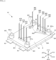
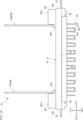
- FIG. 1 is a perspective view showing a semiconductor device according to a first embodiment of the present disclosure.
- FIG. 2 is a partial perspective view showing the semiconductor device according to the first embodiment of the present disclosure.
- FIG. 3 is a partial perspective view showing the semiconductor device according to the first embodiment of the present disclosure.
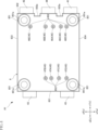
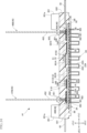
- FIG. 4 is a plan view showing the semiconductor device according to the first embodiment of the present disclosure.
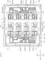
- FIG. 5 is a partial plan view showing the semiconductor device according to the first embodiment of the present disclosure.
- FIG. 6 is a partial side view showing the semiconductor device according to the first embodiment of the present disclosure.
- FIG. 7 is a partial enlarged plan view showing the semiconductor device according to the first embodiment of the present disclosure.
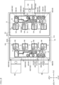
- FIG. 8 is a partial plan view showing the semiconductor device according to the first embodiment of the present disclosure.
- FIG. 1 is a perspective view showing a semiconductor device according to a first embodiment of the present disclosure.
- FIG. 2 is a partial perspective view showing the semiconductor device according to the first embodiment of the present disclosure.
- FIG. 9 is a partial plan view showing the semiconductor device according to the first embodiment of the present disclosure.
- FIG. 10 is a side view showing the semiconductor device according to the first embodiment of the present disclosure.
- FIG. 11 is a bottom view showing the semiconductor device according to the first embodiment of the present disclosure.
- FIG. 12 is a partial bottom view showing the semiconductor device according to the first embodiment of the present disclosure.
- FIG. 13 is a cross-sectional view taken along line XIII-XIII in FIG.
- FIG. 14 is a cross-sectional view taken along line XIV-XIV in FIG.
- FIG. 15 is a partially enlarged cross-sectional view showing the semiconductor device according to the first embodiment of the present disclosure.
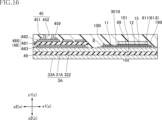
- FIG. 16 is a partially enlarged cross-sectional view showing the semiconductor device according to the first embodiment of the present disclosure.
- FIG. 17 is a cross-sectional view taken along line XVII-XVII in FIG.
- FIG. 18 is a cross-sectional view taken along line XVIII-XVIII in FIG.
- FIG. 19 is a cross-sectional view taken along line XIX-XIX in FIG.
- FIG. 20 is a cross-sectional view taken along line XX-XX in FIG.
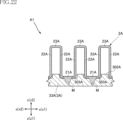
- FIG. 21 is a cross-sectional view taken along line XXI-XXI in FIG. 22 is a partially enlarged cross-sectional view taken along line XXII-XXII in FIG.
- FIG. 23 is a cross-sectional view showing the power conversion unit according to the first embodiment of the present disclosure.
- FIG. 24 is a cross-sectional view showing the power conversion unit according to the first embodiment of the present disclosure.
- FIG. 25 is a bottom view showing a semiconductor device according to a second embodiment of the present disclosure.
- FIG. 26 is a bottom view showing a semiconductor device according to a second embodiment of the present disclosure.
- 27 is a partially enlarged cross-sectional view taken along line XXVI-XXVI in FIG. 25.
- FIG. 28 is a side view showing a semiconductor device according to a third embodiment of the present disclosure.
- an object A is formed on an object B" and “an object A is formed on an object B” include “an object A is formed directly on an object B” and “an object A is formed on an object B with another object interposed between the object A and the object B” unless otherwise specified.
- an object A is disposed on an object B” and “an object A is disposed on an object B” include “an object A is disposed directly on an object B” and “an object A is disposed on an object B with another object interposed between the object A and the object B" unless otherwise specified.
- an object A is located on an object B includes “an object A is located on an object B in contact with an object B” and “an object A is located on an object B with another object interposed between the object A and the object B” unless otherwise specified.
- an object A overlaps an object B when viewed in a certain direction includes “an object A overlaps the entire object B” and “an object A overlaps a part of an object B.”
- a surface A faces (one side or the other side of) direction B” is not limited to the case where the angle of surface A with respect to direction B is 90 degrees, but also includes the case where surface A is tilted with respect to direction B.
- First embodiment: 1 to 24 show a semiconductor device and a power conversion unit according to a first embodiment of the present disclosure.
- the semiconductor device A1 of this embodiment includes a plurality of first semiconductor elements 10A, a plurality of second semiconductor elements 10B, a first heat dissipation member 2A, a first substrate 3A, a first terminal 41, a second terminal 42, a plurality of third terminals 43, a fourth terminal 44, a plurality of control terminals 45, a control terminal support 48, a first conductive member 5, a second conductive member 6, and a sealing resin 8.
- FIG. 1 is a perspective view showing the semiconductor device A1.
- FIG. 2 is a partial perspective view showing the semiconductor device A1.
- FIG. 3 is a partial perspective view showing the semiconductor device A1.
- FIG. 4 is a plan view showing the semiconductor device A1.
- FIG. 5 is a partial plan view showing the semiconductor device A1.
- FIG. 6 is a partial side view showing the semiconductor device A1.
- FIG. 7 is a partial enlarged plan view showing the semiconductor device A1.
- FIG. 8 is a partial plan view showing the semiconductor device A1.
- FIG. 9 is a partial plan view showing the semiconductor device A1.
- FIG. 10 is a side view showing the semiconductor device A1.
- FIG. 11 is a bottom view showing the semiconductor device A1.
- FIG. 12 is a partial bottom view showing the semiconductor device A1.
- FIG. 1 is a perspective view showing the semiconductor device A1.
- FIG. 2 is a partial perspective view showing the semiconductor device A1.
- FIG. 3 is a partial perspective view showing the semiconductor device A1.
- FIG. 13 is a cross-sectional view taken along line XIII-XIII in FIG. 5.
- FIG. 14 is a cross-sectional view taken along line XIV-XIV in FIG. 5.
- FIG. 15 is a partial enlarged cross-sectional view showing the semiconductor device A1.
- FIG. 16 is a partial enlarged cross-sectional view showing the semiconductor device A1.
- FIG. 17 is a cross-sectional view taken along line XVII-XVII in FIG. 5.
- FIG. 18 is a cross-sectional view taken along line XVIII-XVIII in FIG. 5.
- FIG. 19 is a cross-sectional view taken along line XIX-XIX in FIG. 5.
- FIG. 20 is a cross-sectional view taken along line XX-XX in FIG. 5.
- FIG. 21 is a cross-sectional view taken along line XXI-XXI in FIG. 5.
- FIG. 22 is a partially enlarged cross-sectional view taken along line XXII-XXII in FIG. 11.
- FIGs. 23 and 24 are cross-sectional views showing power conversion unit B1.
- one side in the first direction x is called the x1 side, and the other side in the first direction x is called the x2 side.
- the second direction y and the thickness direction z are the same sides in the first direction x.
- First semiconductor element 10A, second semiconductor element 10B The first semiconductor elements 10A and the second semiconductor elements 10B are electronic components that are the core of the functions of the semiconductor device A1.
- the material of each of the first semiconductor elements 10A and the second semiconductor elements 10B is a semiconductor material mainly made of, for example, SiC (silicon carbide). This semiconductor material is not limited to SiC, and may be Si (silicon), GaN (gallium nitride), or C (diamond).
- Each of the first semiconductor elements 10A and the second semiconductor elements 10B is, for example, a power semiconductor chip having a switching function such as a MOSFET (Metal Oxide Semiconductor Field Effect Transistor).
- MOSFET Metal Oxide Semiconductor Field Effect Transistor
- the first semiconductor element 10A and the second semiconductor element 10B are shown as MOSFETs, but are not limited thereto and may be other transistors such as an IGBT (Insulated Gate Bipolar Transistor).
- IGBT Insulated Gate Bipolar Transistor
- Each of the first semiconductor elements 10A and each of the second semiconductor elements 10B are the same element.
- Each of the first semiconductor elements 10A and each of the second semiconductor elements 10B is, for example, an n-channel MOSFET, but may be a p-channel MOSFET.
- the first semiconductor element 10A and the second semiconductor element 10B each have an element main surface 101 and an element back surface 102.
- the element main surface 101 and the element back surface 102 are separated in the thickness direction z.
- the element main surface 101 faces the z1 side in the thickness direction z
- the element back surface 102 faces the z2 side in the thickness direction z.
- the semiconductor device A1 has four first semiconductor elements 10A and four second semiconductor elements 10B, but the number of first semiconductor elements 10A and the number of second semiconductor elements 10B are not limited to this configuration and are changed as appropriate according to the performance required of the semiconductor device A1.
- four first semiconductor elements 10A and four second semiconductor elements 10B are arranged.
- the number of first semiconductor elements 10A and the number of second semiconductor elements 10B may be two or three, or five or more.
- the number of first semiconductor elements 10A and the number of second semiconductor elements 10B may be equal to or different from each other.
- the number of first semiconductor elements 10A and the number of second semiconductor elements 10B are determined by the current capacity handled by the semiconductor device A1.
- the semiconductor device A1 is configured, for example, as a half-bridge type switching circuit.
- the multiple first semiconductor elements 10A configure the upper arm circuit of the semiconductor device A1
- the multiple second semiconductor elements 10B configure the lower arm circuit.
- the multiple first semiconductor elements 10A are connected in parallel to each other, and in the lower arm circuit, the multiple second semiconductor elements 10B are connected in parallel to each other.
- Each first semiconductor element 10A and each second semiconductor element 10B are connected in series to configure a bridge layer.
- each of the first semiconductor elements 10A is mounted on a first conductive portion 321 of a first substrate 3A described later.
- the first semiconductor elements 10A are arranged, for example, in the second direction y and are spaced apart from each other.
- Each of the first semiconductor elements 10A is conductively bonded to the first conductive portion 321 via a first conductive bonding material 19A.
- the first semiconductor elements 10A may be mounted on a metal member other than a part of the DBC substrate or the like.
- the metal member corresponds to the first conductive portion in this disclosure. This metal member may be supported by, for example, the first conductive portion 321.
- each of the second semiconductor elements 10B is mounted on the second conductive portion 322 of the first substrate 3A described later.
- the second semiconductor elements 10B are arranged, for example, in the second direction y and are spaced apart from each other.
- Each second semiconductor element 10B is conductively bonded to the second conductive portion 322 via the second conductive bonding material 19B.
- the element back surface 102 faces the second conductive portion 322.
- the first semiconductor elements 10A and the second semiconductor elements 10B overlap in the first direction x, but they do not have to overlap.
- the second semiconductor elements 10B may be mounted on a metal member different from a part of the DBC substrate or the like.
- the metal member corresponds to the second conductive portion in this disclosure. This metal member may be supported, for example, by the second conductive part 322.
- the first semiconductor elements 10A and the second semiconductor elements 10B each have a first principal surface electrode 11, a second principal surface electrode 12, a third principal surface electrode 13, and a back surface electrode 15.
- the configurations of the first principal surface electrode 11, the second principal surface electrode 12, the third principal surface electrode 13, and the back surface electrode 15 described below are common to each of the first semiconductor elements 10A and each of the second semiconductor elements 10B.
- the first principal surface electrode 11, the second principal surface electrode 12, and the third principal surface electrode 13 are provided on the element principal surface 101.
- the first principal surface electrode 11, the second principal surface electrode 12, and the third principal surface electrode 13 are insulated by an insulating film (not shown).
- the back surface electrode 15 is provided on the element back surface 102.
- the first principal surface electrode 11 is, for example, a gate electrode, and a drive signal (for example, a gate voltage) for driving the first semiconductor element 10A (second semiconductor element 10B) is input.
- the second principal surface electrode 12 is, for example, a source electrode, through which a source current flows.
- the second principal surface electrode 12 in this embodiment has a gate finger 121.
- the gate finger 121 is, for example, made of a linear insulator extending in the first direction x, and divides the second principal surface electrode 12 into two in the second direction y.
- the third principal surface electrode 13 is, for example, a source sense electrode, through which a source current flows.
- the back surface electrode 15 is, for example, a drain electrode, through which a drain current flows.
- the back surface electrode 15 covers the entire area (or substantially the entire area) of the element back surface 102.
- the back surface electrode 15 is, for example, made of Ag (silver) plating.
- each first semiconductor element 10A switches between a conductive state and a cut-off state in response to the drive signal.
- a current flows from the back surface electrode 15 (drain electrode) to the second principal surface electrode 12 (source electrode), and in the cut-off state, this current does not flow.
- each first semiconductor element 10A performs a switching operation.
- the semiconductor device A1 converts a DC voltage input between the one fourth terminal 44 and the two first terminals 41 and the second terminals 42 into, for example, an AC voltage by the switching function of the multiple first semiconductor elements 10A and the multiple second semiconductor elements 10B, and outputs the AC voltage from the third terminal 43.
- the semiconductor device A1 includes a thermistor 17.
- the thermistor 17 is used as a temperature detection sensor.
- the semiconductor device A1 may include, for example, a temperature sensing diode in addition to the thermistor 17, or may not include the thermistor 17.
- the first substrate 3A supports a plurality of first semiconductor elements 10A and a plurality of second semiconductor elements 10B.
- the specific configuration of the first substrate 3A is not limited in any way, and may be, for example, a DBC (Direct Bonded Copper) substrate or an AMB (Active Metal Brazing) substrate.
- the first substrate 3A includes a first insulating layer 31A, a first main surface metal layer 32A, and a first back surface metal layer 33A.
- the first main surface metal layer 32A includes a first conductive portion 321 and a second conductive portion 322.
- the dimension of the first substrate 3A in the thickness direction z is, for example, 0.4 mm or more and 3.0 mm or less.
- the first insulating layer 31A is, for example, a ceramic with excellent thermal conductivity.
- An example of such a ceramic is SiN (silicon nitride).
- the first insulating layer 31A is not limited to ceramics and may be an insulating resin sheet or the like.
- the first insulating layer 31A is, for example, rectangular in plan view.
- the dimension of the first insulating layer 31A in the thickness direction z is, for example, 0.05 mm or more and 1.0 mm or less.
- the first conductive portion 321 supports a plurality of first semiconductor elements 10A
- the second conductive portion 322 supports a plurality of second semiconductor elements 10B.
- the first conductive portion 321 and the second conductive portion 322 are formed on the upper surface (the surface facing the z1 side in the thickness direction z) of the first insulating layer 31A.
- the constituent material of the first conductive portion 321 and the second conductive portion 322 includes, for example, Cu (copper).
- the constituent material may include, for example, Al (aluminum) other than Cu (copper).
- the first conductive portion 321 and the second conductive portion 322 are spaced apart in the first direction x.
- the first conductive portion 321 is located on the x1 side of the second conductive portion 322 in the first direction x.
- the first conductive portion 321 and the second conductive portion 322 are each, for example, rectangular in a plan view.
- the first conductive part 321 and the second conductive part 322, together with the first conductive member 5 and the second conductive member 6, form a path for the main circuit current that is switched by the multiple first semiconductor elements 10A and the multiple second semiconductor elements 10B.
- the first conductive portion 321 has a first main surface 301A.
- the first main surface 301A is a plane facing the z1 side in the thickness direction z.
- a plurality of first semiconductor elements 10A are bonded to the first main surface 301A of the first conductive portion 321 via a first conductive bonding material 19A.
- the second conductive portion 322 has a second main surface 301B.
- the second main surface 301B is a plane facing the z1 side in the thickness direction z.
- a plurality of second semiconductor elements 10B are bonded to the second main surface 301B of the second conductive portion 322 via a second conductive bonding material 19B.
- the constituent materials of the first conductive bonding material 19A and the second conductive bonding material 19B are not particularly limited, and may be, for example, solder, a metal paste material containing a metal such as Ag (silver), or a sintered metal containing a metal such as Ag (silver).
- the dimension of the first conductive part 321 and the second conductive part 322 in the thickness direction z is, for example, 0.1 mm or more and 1.5 mm or less.
- the first back surface metal layer 33A is formed on the lower surface (surface facing the z2 side in the thickness direction z) of the first insulating layer 31A.
- the constituent material of the first back surface metal layer 33A is the same as the constituent material of the first main surface metal layer 32A.
- the first back surface metal layer 33A has a first back surface 302A and a plurality of first recesses 303A.
- the first back surface 302A is a flat surface facing the z2 side in the thickness direction z.
- the first back surface 302A is exposed from the sealing resin 8.
- the first back surface metal layer 33A overlaps both the first conductive portion 321 and the second conductive portion 322 in a plan view.
- each of the multiple first recesses 303A is recessed from the first back surface 302A toward the z1 side in the thickness direction z.
- the multiple first recesses 303A are arranged in the first direction x.
- the first recesses 303A in this embodiment are grooves extending in the second direction y.
- First heat dissipation member 2A As shown in Figures 2, 6, 10 to 14, and 17 to 22, the first heat dissipation member 2A is disposed on the z2 side of the first substrate 3A (first back surface metal layer 33A) in the thickness direction z.
- the first heat dissipation member 2A has a plurality of first base portions 21A, a plurality of first upright portions 22A, and a plurality of first connecting portions 23A.
- the material of the first heat dissipation member 2A is not limited in any way, and it is formed, for example, using a metal plate material.
- the metal plate material includes metals such as Cu (copper), Al (aluminum), and stainless steel, or alloys thereof.
- the first bases 21A are located on the z1 side in the thickness direction z.
- the first bases 21A are individually accommodated in the first recesses 303A.
- the first bases 21A are joined to the first back surface metal layer 33A in the first recess 303A.
- the method of joining the first base 21A to the first back surface metal layer 33A is not limited in any way, and may be appropriately selected from welding methods such as laser welding, methods using joints such as brazing, ultrasonic bonding, solid-phase diffusion bonding, and the like.
- the first base 21A is joined to the first back surface metal layer 33A by laser bonding.
- a weld M is formed in which a part of the first base 21A and the first back surface metal layer 33A are melted and then solidified.
- the thickness of the first base 21A in the thickness direction z is thinner than the depth of the first recess 303A in the thickness direction z.
- the shape of the first base portion 21A is not limited in any way, and in this embodiment, it is a strip extending in the second direction y.
- the first base portion 21A may have a size and shape that fits into the first recess 303A, or may be slightly smaller than the first recess 303A.
- the first standing portions 22A are individually connected to both ends of the first base portions 21A in the first direction x, and stand along the thickness direction z.
- the first standing portions 22A protrude further toward the z2 side in the thickness direction z than the first back surface 302A.
- the length of the first standing portions 22A in the second direction y and the length of the first base portions 21A in the second direction y are the same (or approximately the same).
- the first standing portions 22A are, for example, strip-shaped extending in the second direction y.
- the multiple first connecting portions 23A connect the z2 side ends of adjacent first standing portions 22A in the first direction x in the thickness direction z.
- the length in the second direction y of the first connecting portion 23A and the length in the second direction y of the first standing portion 22A are the same (or approximately the same).
- the shape of the first connecting portion 23A viewed from the thickness direction z is not limited in any way, and in this embodiment, it is a band shape.
- the shape of the first connecting portion 23A viewed from the second direction y is not limited in any way, and may be a flat shape along the first direction x as shown in the figure, or a dome shape or mountain shape bulging out toward the z2 side in the thickness direction z.
- First terminal 41, second terminal 42, third terminal 43, fourth terminal 44 The first terminal 41, the second terminal 42, the plurality of third terminals 43, and the fourth terminal 44 are each made of a plate-shaped metal plate.
- the metal plate contains, for example, Cu (copper) or a Cu (copper) alloy.
- the semiconductor device A1 includes one each of the first terminal 41, the second terminal 42, and the fourth terminal 44, and two third terminals 43, but the number of each terminal is not limited in any way.
- the DC voltage to be converted is input to the first terminal 41, the second terminal 42, and the fourth terminal 44.
- the fourth terminal 44 is a positive electrode (P terminal), and the first terminal 41 and the second terminal 42 are negative electrodes (N terminals).
- the AC voltage converted by the first semiconductor element 10A and the second semiconductor element 10B is output from the multiple third terminals 43.
- the first terminal 41, the second terminal 42, the multiple third terminals 43, and the fourth terminal 44 each include a portion covered by the sealing resin 8 and a portion exposed from the sealing resin 8.
- the fourth terminal 44 is conductively joined to the first conductive portion 321 as shown in FIG. 14. There are no limitations on the method of conductive joining, and methods such as ultrasonic bonding, laser bonding, welding, or methods using solder, metal paste, sintered silver, etc. may be appropriately adopted. As shown in FIG. 8, FIG. 9, etc., the fourth terminal 44 is located on the x1 side of the first direction x with respect to the multiple first semiconductor elements 10A and the first conductive portion 321. The fourth terminal 44 is conductive to the first conductive portion 321, and is also conductive to the back electrode 15 (drain electrode) of each first semiconductor element 10A via the first conductive portion 321.
- the first terminal 41 and the second terminal 42 are electrically connected to the second conductive member 6.
- the first terminal 41 and the second conductive member 6 are integrally formed.
- the first terminal 41 and the second conductive member 6 are integrally formed, for example, by performing cutting and bending processes on a single metal plate material, and do not include a bonding material for bonding them to each other.
- the second terminal 42 and the second conductive member 6 are integrally formed. Note that the first terminal 41 and the second terminal 42 may be configured to be electrically connected to the second conductive member 6, and may have a bonding portion that bonds them to each other, unlike this embodiment.
- the first terminal 41 and the second terminal 42 are located on the x1 side of the first direction x with respect to the multiple first semiconductor elements 10A and the first conductive portion 321, as shown in Figures 5 and 8.
- the first terminal 41 and the second terminal 42 are each electrically connected to the second conductive member 6, and are also electrically connected to the second principal surface electrode 12 (source electrode) of each second semiconductor element 10B via the second conductive member 6.
- the first terminal 41, the second terminal 42, and the fourth terminal 44 each protrude from the sealing resin 8 to the x1 side in the first direction x in the semiconductor device A1.
- the first terminal 41, the second terminal 42, and the fourth terminal 44 are spaced apart from one another.
- the first terminal 41 and the second terminal 42 are located on opposite sides of the fourth terminal 44 in the second direction y.
- the first terminal 41 is located on the y1 side of the fourth terminal 44 in the second direction y
- the second terminal 42 is located on the y2 side of the fourth terminal 44 in the second direction y.
- the first terminal 41, the second terminal 42, and the fourth terminal 44 overlap one another when viewed in the second direction y.
- the two third terminals 43 are conductively joined to the second conductive portion 322, as can be seen from FIG. 8, FIG. 9, and FIG. 13.
- the conductive joining method is not limited in any way, and methods such as ultrasonic bonding, laser bonding, welding, or methods using solder, metal paste, silver sintered body, etc. are appropriately adopted.
- the two third terminals 43 are located on the x2 side of the first direction x with respect to the multiple second semiconductor elements 10B and the second conductive portion 322.
- Each third terminal 43 is conductive to the second conductive portion 322 and is conductive to the back electrode 15 (drain electrode) of each second semiconductor element 10B via the second conductive portion 322.
- the number of third terminals 43 is not limited to two, and may be, for example, one, or may be three or more. For example, when there is one third terminal 43, it is desirable that it is connected to the center part of the second conductive portion 322 in the second direction y.
- the multiple control terminals 45 are pin-shaped terminals for controlling each of the first semiconductor elements 10A and each of the second semiconductor elements 10B.
- the multiple control terminals 45 include multiple first control terminals 46A-46E and multiple second control terminals 47A-47D.
- the multiple first control terminals 46A-46E are used to control each of the first semiconductor elements 10A, etc.
- the multiple second control terminals 47A-47D are used to control each of the second semiconductor elements 10B, etc.
- First control terminals 46A to 46E The multiple first control terminals 46A-46E are arranged at intervals in the second direction y. As shown in Figures 8, 14, 21, etc., each of the first control terminals 46A-46E is supported by the first conductive portion 321 via a control terminal support body 48 (first support portion 48A described below). As shown in Figures 5 and 8, each of the first control terminals 46A-46E is located between the multiple first semiconductor elements 10A and the first terminal 41, the second terminal 42, and the fourth terminal 44 in the first direction x.
- the first control terminal 46A is a terminal (gate terminal) for inputting a drive signal to the multiple first semiconductor elements 10A.
- a drive signal for driving the multiple first semiconductor elements 10A is input to the first control terminal 46A (for example, a gate voltage is applied).
- the first control terminal 46B is a terminal (source sense terminal) for detecting source signals of the multiple first semiconductor elements 10A.
- the first control terminal 46B detects the voltage (voltage corresponding to the source current) applied to each second principal surface electrode 12 (source electrode) of the multiple first semiconductor elements 10A.
- the first control terminal 46C and the first control terminal 46D are terminals that are electrically connected to thermistor 17.
- the first control terminal 46E is a terminal (drain sense terminal) for detecting the drain signals of the multiple first semiconductor elements 10A.
- the first control terminal 46E detects the voltage (voltage corresponding to the drain current) applied to each back electrode 15 (drain electrode) of the multiple first semiconductor elements 10A.
- the second control terminals 47A-47D are spaced apart in the second direction y. As shown in Figures 8 and 14, each of the second control terminals 47A-47D is supported by the second conductive portion 322 via a control terminal support 48 (second support portion 48B, described below). As shown in Figures 5 and 8, each of the second control terminals 47A-47D is located between the second semiconductor elements 10B and the two third terminals 43 in the first direction x.
- the second control terminal 47A is a terminal (gate terminal) for inputting a drive signal for the multiple second semiconductor elements 10B.
- a drive signal for driving the multiple second semiconductor elements 10B is input to the second control terminal 47A (for example, a gate voltage is applied).
- the second control terminal 47B is a terminal (source sense terminal) for detecting source signals of the multiple second semiconductor elements 10B.
- the second control terminal 47B detects a voltage (voltage corresponding to a source current) applied to each second principal surface electrode 12 (source electrode) of the multiple second semiconductor elements 10B.
- the second control terminal 47C and the second control terminal 47D are terminals that are conductive to the thermistor 17.
- Each of the multiple control terminals 45 includes a holder 451 and a metal pin 452.
- the holder 451 is made of a conductive material. As shown in Figures 15 and 16, the holder 451 is bonded to the control terminal support 48 (first metal layer 482 described below) via a conductive bonding material 459.
- the holder 451 includes a cylindrical portion, an upper end flange, and a lower end flange. The upper end flange is connected to the upper part of the cylindrical portion, and the lower end flange is connected to the lower part of the cylindrical portion.
- a metal pin 452 is inserted through at least the upper end flange and the cylindrical portion of the holder 451.
- the holder 451 is covered with sealing resin 8 (second protrusion 852 described below).
- the metal pin 452 is a rod-shaped member extending in the thickness direction z.
- the metal pin 452 is supported by being pressed into the holder 451.
- the metal pin 452 is electrically connected to the control terminal support 48 (first metal layer 482 described below) at least via the holder 451.
- the control terminal support 48 first metal layer 482 described below
- the metal pin 452 is electrically connected to the control terminal support 48 via the conductive bonding material 459.
- Control terminal support 48 The control terminal support body 48 supports the plurality of control terminals 45.
- the control terminal support body 48 is interposed between the first main surface 301A and the plurality of control terminals 45 and between the second main surface 301B and the first main surface 301A and the second main surface 301B in the thickness direction z.
- the control terminal support 48 includes a first support portion 48A and a second support portion 48B.
- the first support portion 48A is disposed on the first conductive portion 321 and supports the first control terminals 46A to 46E of the control terminals 45.
- the first support portion 48A is bonded to the first conductive portion 321 via a bonding material 49 as shown in FIG. 15.
- the bonding material 49 may be conductive or insulating, and may be, for example, solder.
- the second support portion 48B is disposed on the second conductive portion 322 and supports the second control terminals 47A to 47D of the control terminals 45.
- the second support portion 48B is bonded to the second conductive portion 322 via a bonding material 49 as shown in FIG. 16.
- the control terminal support 48 (each of the first support portion 48A and the second support portion 48B) is formed, for example, from a DBC (Direct Bonded Copper) substrate.
- the control terminal support 48 has an insulating layer 481, a first metal layer 482, and a second metal layer 483 stacked on top of each other.
- the insulating layer 481 is made of, for example, ceramics.
- the insulating layer 481 is, for example, rectangular in plan view.
- the first metal layer 482 is formed on the upper surface of the insulating layer 481, as shown in FIG. 15, FIG. 16, etc. Each control terminal 45 is provided upright on the first metal layer 482.
- the first metal layer 482 includes, for example, Cu (copper) or a Cu (copper) alloy. As shown in FIG. 8, etc., the first metal layer 482 includes a first portion 482A, a second portion 482B, a third portion 482C, a fourth portion 482D, a fifth portion 482E, and a sixth portion 482F.
- the first portion 482A, the second portion 482B, the third portion 482C, the fourth portion 482D, the fifth portion 482E, and the sixth portion 482F are separated and insulated from each other.
- the first portion 482A has a plurality of wires 71 bonded thereto, and is electrically connected to the first principal surface electrodes 11 (gate electrodes) of the first semiconductor elements 10A (second semiconductor elements 10B) via the respective wires 71.
- the first portion 482A and the sixth portion 482F are connected to a plurality of wires 73.
- the sixth portion 482F is electrically connected to the first principal surface electrodes 11 (gate electrodes) of the first semiconductor elements 10A (second semiconductor elements 10B) via the wires 73 and 71.
- the first control terminal 46A is bonded to the sixth portion 482F of the first support 48A
- the second control terminal 47A is bonded to the sixth portion 482F of the second support 48B.
- the second portion 482B has a plurality of wires 72 joined thereto, and is electrically connected to the third principal surface electrode 13 (source sense electrode) of each of the first semiconductor elements 10A (each of the second semiconductor elements 10B) via each of the wires 72.
- the first control terminal 46B is joined to the second portion 482B of the first support 48A, and the second control terminal 47B is joined to the second portion 482B of the second support 48B.
- the thermistor 17 is joined to the third portion 482C and the fourth portion 482D. As shown in FIG. 8, the first control terminals 46C and 46D are joined to the third portion 482C and the fourth portion 482D of the first support portion 48A, and the second control terminals 47C and 47D are joined to the third portion 482C and the fourth portion 482D of the second support portion 48B.
- the fifth portion 482E of the first support portion 48A is joined to a wire 74, and is electrically connected to the first conductive portion 321 via the wire 74. As shown in FIG. 8, the first control terminal 46E is joined to the fifth portion 482E of the first support portion 48A. The fifth portion 482E of the second support portion 48B is not electrically connected to other components.
- Each of the wires 71 to 74 is, for example, a bonding wire.
- the material of each of the wires 71 to 74 includes, for example, any of Au (gold), Al (aluminum), or Cu (copper).
- the second metal layer 483 is formed on the lower surface of the insulating layer 481, as shown in Figures 15 and 16.
- the second metal layer 483 of the first support portion 48A is bonded to the first conductive portion 321 via a bonding material 49, as shown in Figure 15.
- the second metal layer 483 of the second support portion 48B is bonded to the second conductive portion 322 via a bonding material 49, as shown in Figure 16.
- First conductive member 5, second conductive member 6 The first conductive member 5 and the second conductive member 6, together with the first conductive portion 321 and the second conductive portion 322, constitute a path of a main circuit current switched by the first semiconductor elements 10A and the second semiconductor elements 10B.
- the first conductive member 5 and the second conductive member 6 are spaced apart from the first main surface 301A and the second main surface 301B on the z1 side in the thickness direction z, and overlap the first main surface 301A and the second main surface 301B in a plan view.
- the first conductive member 5 and the second conductive member 6 are each made of a metal plate material.
- the metal includes, for example, Cu (copper) or a Cu (copper) alloy.
- the first conductive member 5 and the second conductive member 6 are metal plate materials that are appropriately bent.
- the first conductive member 5 is connected to the second principal surface electrode 12 (source electrode) and the second conductive portion 322 of each first semiconductor element 10A, and provides electrical continuity between the second principal surface electrode 12 and the second conductive portion 322 of each first semiconductor element 10A.
- the first conductive member 5 forms a path for the main circuit current that is switched by the multiple first semiconductor elements 10A.
- the first conductive member 5 includes a main portion 51, multiple first joints 52, and multiple second joints 53.
- the main portion 51 is located between the multiple first semiconductor elements 10A and the second conductive portion 322 in the first direction x, and is a band-shaped portion extending in the second direction y in a plan view.
- the main portion 51 overlaps both the first conductive portion 321 and the second conductive portion 322 in a plan view, and is separated from the first main surface 301A and the second main surface 301B on the z1 side in the thickness direction z in the thickness direction z. As shown in FIG.
- the main portion 51 is located on the z2 side in the thickness direction z with respect to the third path portion 66 and the fourth path portion 67 of the second conductive member 6 described later, and is located closer to the first main surface 301A and the second main surface 301B than the third path portion 66 and the fourth path portion 67.
- the main portion 51 is arranged parallel to the first main surface 301A and the second main surface 301B.
- the main portion 51 extends continuously in the second direction y corresponding to the region in which the multiple first semiconductor elements 10A are arranged.
- multiple first openings 514 are formed in the main portion 51.
- Each of the multiple first openings 514 is, for example, a through hole penetrating in the thickness direction z (the plate thickness direction of the main portion 51).
- the multiple first openings 514 are arranged at intervals in the second direction y.
- the multiple first openings 514 are provided corresponding to each of the multiple first semiconductor elements 10A.
- four first openings 514 are provided in the main portion 51, and the first openings 514 and the multiple (four) first semiconductor elements 10A are located at the same position in the second direction y.
- each first opening 514 overlaps with the gap between the first conductive portion 321 and the second conductive portion 322 in a plan view.
- the multiple first openings 514 are formed to facilitate the flow of the resin material between the upper side (z1 side in the thickness direction z) and the lower side (z2 side in the thickness direction z) near the main portion 51 (first conductive member 5) when injecting a fluid resin material to form the sealing resin 8.
- each first joint 52 and the multiple second joints 53 are connected to the main part 51 and are arranged corresponding to the multiple first semiconductor elements 10A.
- each first joint 52 is located on the x1 side of the first direction x with respect to the main part 51.
- Each second joint 53 is located on the x2 side of the first direction x with respect to the main part 51.
- each first joint 52 and the corresponding second main surface electrode 12 of any of the first semiconductor elements 10A are joined via a conductive joint material 59.
- Each second joint 53 and the second conductive part 322 are joined via a conductive joint material 59.
- the material of the conductive joint material 59 is not particularly limited, and may be, for example, solder, a metal paste material, or a sintered metal.
- the first joint 52 has two parts spaced apart in the second direction y. These two parts are joined to the second principal surface electrode 12 on both sides in the second direction y, sandwiching the gate finger 121 of the second principal surface electrode 12 of the first semiconductor element 10A.
- the second conductive member 6 electrically connects the second main surface electrode 12 (source electrode) of each second semiconductor element 10B to the first terminal 41 and the second terminal 42.
- the second conductive member 6 is integrally formed with the first terminal 41 and the second terminal 42.
- the second conductive member 6 constitutes a path of the main circuit current switched by the multiple second semiconductor elements 10B.
- the second conductive member 6 includes multiple third joints 61, a first path portion 64, a second path portion 65, multiple third path portions 66, and a fourth path portion 67.
- the second conductive member 6 also includes a first step portion 602 and a second step portion 603.
- the multiple third joints 61 are portions that are individually joined to the multiple second semiconductor elements 10B.
- Each third joint 61 and the second principal surface electrode 12 of each second semiconductor element 10B are joined via a conductive joint material 69.
- the material of the conductive joint material 69 is not particularly limited, and may be, for example, solder, a metal paste material, or a sintered metal.
- the third joint 61 has two flat portions 611 and two first inclined portions 612.
- the two flat portions 611 are aligned in the second direction y.
- the two flat portions 611 are spaced apart from each other in the second direction y.
- the shape of the flat portion 611 is not limited in any way, and in the illustrated example, it is rectangular.
- the two flat portions are joined to the second principal surface electrode 12 on both sides in the second direction y, sandwiching the gate finger 121 of the second principal surface electrode 12 of the second semiconductor element 10B therebetween.
- the two first inclined portions 612 are connected to the outside of the two flat portions 611 in the second direction y. That is, the first inclined portion 612 located on the y1 side of the second direction y is connected to the y1 side of the flat portion 611 located on the y1 side of the second direction y. Also, the first inclined portion 612 located on the y2 side of the second direction y is connected to the y2 side of the second direction y to the y2 side of the flat portion 611 located on the y2 side of the second direction y.
- the first inclined portion 612 is inclined so that the further it is from the flat portion 611 in the second direction y, the closer it is to the z1 side in the thickness direction z.
- the first path portion 64 is interposed between the multiple third joint portions 61 and the first terminal 41.
- the first path portion 64 is connected to the first terminal 41 via a first step portion 602.
- the first path portion 64 overlaps the first conductive portion 321.
- the first path portion 64 has a shape that extends overall in the first direction x.
- the first path portion 64 includes a first band portion 641 and a first extension portion 643.
- the first band portion 641 is located on the x2 side of the first direction x with respect to the first terminal 41, and is parallel (or approximately parallel) to the first main surface 301A.
- the first band portion 641 has a shape that extends in the first direction x as a whole.
- the first band portion 641 has a recess 649.
- the recess 649 is a portion where a part of the first band portion 641 is recessed toward the y1 side of the second direction y. In FIG. 5, the first metal portion 35 appears through the recess 649.
- the first extension portion 643 extends from the side end of the first band portion 641 on the y1 side in the second direction y to the z2 side in the thickness direction z.
- the first extension portion 643 is spaced apart from the first conductive portion 321.
- the first extension portion 643 is shaped along the thickness direction z and has an elongated rectangular shape with the first direction x as the longitudinal direction. Note that the first path portion 64 may not have the first extension portion 643.
- the second path portion 65 is interposed between the multiple third joint portions 61 and the second terminal 42.
- the second path portion 65 is connected to the second terminal 42 via the second step portion 603.
- the second path portion 65 overlaps the first conductive portion 321.
- the second path portion 65 has a shape that extends overall in the first direction x.
- the second path portion 65 includes a second band portion 651 and a second extension portion 653.
- the second band portion 651 is located on the x2 side of the first direction x with respect to the second terminal 42, and is parallel (or approximately parallel) to the first main surface 301A.
- the second band portion 651 has a shape that extends in the first direction x as a whole.
- the second band portion 651 has a recess 659.
- the recess 659 is a portion where a part of the second band portion 651 is recessed toward the y2 side of the second direction y. In FIG. 5, the second metal portion 36 appears through the recess 659.
- the second extension portion 653 extends from the side end of the second band portion 651 on the y2 side in the second direction y to the z2 side in the thickness direction z.
- the second extension portion 653 is spaced apart from the first conductive portion 321.
- the second extension portion 653 has a shape that follows the thickness direction z and is an elongated rectangle with the first direction x as the longitudinal direction. Note that the second path portion 65 may not have a second extension portion 653.
- the multiple third path portions 66 are individually connected to the multiple third joint portions 61.
- Each third path portion 66 has a shape extending in the first direction x, and is arranged at a distance from one another in the second direction y. There is no limitation on the number of multiple third path portions 66, and in the illustrated example, five third path portions 66 are arranged.
- Each third path portion 66 is arranged so as to be located between the multiple second semiconductor elements 10B in the second direction y, or to be located outside the multiple second semiconductor elements 10B in the second direction y.
- the two third path portions 66 located on both outer sides in the second direction y have recesses 669 formed therein.
- the recesses 669 are recessed from the inside toward the outside in the second direction y. In the illustrated example, one recess 669 is formed in each of the two third path portions 66. In FIG. 5, the second conductive portion 322 appears through these recesses 669.
- one third joint 61 is disposed between two third path portions 66 adjacent in the second direction y.
- the first inclined portion 612 located on the y1 side in the second direction y is connected to the third path portion 66 located on the y1 side in the second direction y, of the two third path portions 66 adjacent in the second direction y.
- the first inclined portion 612 located on the y2 side in the second direction y is connected to the third path portion 66 located on the y2 side in the second direction y, of the two third path portions 66 adjacent in the second direction y.
- the fourth path portion 67 is connected to the ends of the third path portions 66 on the x1 side in the first direction x.
- the fourth path portion 67 has a shape that extends long in the second direction y.
- the fourth path portion 67 is connected to the ends of the first band portion 641 of the first path portion 64 and the second band portion 651 of the second path portion 65 on the x2 side in the first direction x.
- the first path portion 64 is connected to the end of the fourth path portion 67 on the y1 side in the second direction y.
- the second path portion 65 is connected to the end of the fourth path portion 67 on the y2 side in the second direction y.
- the sealing resin 8 covers the first semiconductor elements 10A, the second semiconductor elements 10B, the first substrate 3A (excluding the first back surface 302A), the first terminal 41, the second terminal 42, the third terminals 43, and a portion of each of the fourth terminals 44, the control terminals 45, the control terminal support 48, the first conductive member 5, the second conductive member 6, and the wires 71 to 74.
- the sealing resin 8 is made of, for example, a black epoxy resin.
- the sealing resin 8 is formed by, for example, molding.
- the sealing resin 8 has, for example, a dimension in the first direction x of about 35 mm to 60 mm, a dimension in the second direction y of about 35 mm to 50 mm, and a dimension in the thickness direction z of about 4 mm to 15 mm. These dimensions are the sizes of the maximum portions along each direction.
- the sealing resin 8 has a resin main surface 81, a resin back surface 82, and a plurality of resin side surfaces 831 to 834.
- the resin main surface 81 and the resin back surface 82 are separated in the thickness direction z, as shown in Figures 10, 13, and 19.
- the resin main surface 81 faces the z1 side in the thickness direction z
- the resin back surface 82 faces the z2 side in the thickness direction z.
- a plurality of control terminals 45 protrude from the resin main surface 81.
- the resin back surface 82 is a frame surrounding the first back surface 302A (the lower surface of the first back surface metal layer 33A) of the first substrate 3A in a plan view.
- the first back surface 302A of the first substrate 3A is exposed from the resin back surface 82 and is, for example, flush with the resin back surface 82.
- the plurality of resin side surfaces 831 to 834 are each connected to both the resin main surface 81 and the resin back surface 82, and are sandwiched between them in the thickness direction z. As shown in FIG. 4 and other figures, the resin side surface 831 and the resin side surface 832 are spaced apart in the first direction x.
- the resin side surface 831 faces the x2 side of the first direction x, and the resin side surface 832 faces the x1 side of the first direction x.
- Two third terminals 43 protrude from the resin side surface 831, and the first terminal 41, the second terminal 42, and the fourth terminal 44 protrude from the resin side surface 832.
- the resin side surface 833 and the resin side surface 834 are spaced apart in the second direction y.
- the resin side surface 833 faces the y2 side of the second direction y
- the resin side surface 834 faces the y1 side of the second direction y.
- a plurality of recesses 832a are formed on the resin side surface 832.
- Each recess 832a is a portion recessed in the first direction x in a plan view.
- the plurality of recesses 832a include those formed between the first terminal 41 and the fourth terminal 44 and those formed between the second terminal 42 and the fourth terminal 44 in a plan view.
- the plurality of recesses 832a are provided to increase the creepage distance along the resin side surface 832 between the first terminal 41 and the fourth terminal 44, and the creepage distance along the resin side surface 832 between the second terminal 42 and the fourth terminal 44.
- the sealing resin 8 has a plurality of first protrusions 851, a plurality of second protrusions 852, and a resin void portion 86.
- the multiple first protrusions 851 each protrude from the resin main surface 81 in the thickness direction z.
- the multiple first protrusions 851 are arranged near the four corners of the sealing resin 8 in a plan view.
- a first protrusion end surface 851a is formed at the tip of each first protrusion 851 (the end on the z1 side in the thickness direction z).
- Each first protrusion end surface 851a of the multiple first protrusions 851 is parallel (or approximately parallel) to the resin main surface 81 and is on the same plane (x-y plane).
- Each first protrusion 851 is, for example, in the shape of a hollow truncated cone with a bottom.
- the multiple first protrusions 851 are used as spacers when the semiconductor device A1 is mounted on a control circuit board or the like of an apparatus that uses the power generated by the semiconductor device A1.
- Each of the multiple first protrusions 851 has a recess 851b and an inner wall surface 851c formed in the recess 851b.
- the shape of each first protrusion 851 may be columnar, and is preferably cylindrical.
- the shape of the recess 851b is preferably cylindrical, and the inner wall surface 851c is preferably a single perfect circle in plan view.
- the sealing resin 8 also has a groove portion 89.
- the groove portion 89 is a portion recessed from the resin back surface 82 toward the z1 side in the thickness direction z.
- the groove portion 89 crosses the resin back surface 82 in the second direction y.
- the sealing resin 8 has two groove portions 89.
- the two groove portions 89 are arranged apart in the first direction x.
- the first back surface metal layer 33A (first back surface 302A) is located between the two groove portions 89.
- the semiconductor device A1 may be mechanically fixed to a control circuit board or the like by a method such as screwing.
- a female screw thread may be formed on the inner wall surface 851c of the recessed portion 851b of the first protrusions 851.
- An insert nut may be embedded in the recessed portion 851b of the first protrusions 851.
- the multiple second protrusions 852 protrude from the resin main surface 81 in the thickness direction z.
- the multiple second protrusions 852 overlap the multiple control terminals 45 in a plan view.
- Each metal pin 452 of the multiple control terminals 45 protrudes from each second protrusion 852.
- Each second protrusion 852 is frustum-shaped.
- the second protrusion 852 covers the holder 451 and a portion of the metal pin 452 in each control terminal 45.
- the power conversion unit B1 includes a semiconductor device A1 and a cooling device 9.
- the cooling device 9 is disposed on the z2 side of the semiconductor device A1 in the thickness direction z.
- the cooling device 9 has a housing 91.
- the housing 91 is a box-shaped member made of metal or resin.
- the housing 91 houses the first heat dissipation member 2A.
- the housing 91 is attached to the semiconductor device A1 via a sealant 919.
- the sealant 919 is sandwiched between the end of the housing 91 and the resin back surface 82 of the sealing resin 8, and keeps the internal space of the housing 91 airtight.
- a groove 911 is formed in the housing 91.
- the groove 911 is annular when viewed from the thickness direction z, and houses a part of the sealant 919.
- the housing 91 is filled with the cooling medium Cm.
- the cooling medium Cm flows within the housing 91.
- the cooling device 9 has a supply unit 92 and a discharge unit 93.
- the supply unit 92 and the discharge unit 93 are attached separately to both sides of the housing 91 in the second direction y.
- the supply unit 92 supplies the cooling medium Cm to the housing 91.
- the discharge unit 93 discharges the cooling medium Cm that has flowed through the housing 91. As a result, the cooling medium Cm flows in the second direction y within the housing 91.
- the cooling medium Cm flowing in the second direction y does not mean that only the flow velocity component in the second direction y exists, but includes a mode in which the cooling medium Cm moves as a whole in the second direction y while including flow velocity components in the first direction x and the thickness direction z.
- the first heat dissipation member 2A has a plurality of first base portions 21A and a plurality of first upright portions 22A.
- the plurality of first upright portions 22A protrude from the first back surface 302A in the thickness direction z, and the heat transfer area can be expanded.
- the first base portion 21A is housed in the first recess 303A and is joined to the first back surface metal layer 33A within the first recess 303A. This allows the first heat dissipation member 2A to be more accurately positioned with respect to the first substrate 3A when attaching the first heat dissipation member 2A to the first substrate 3A after forming the first substrate 3A, the plurality of first semiconductor elements 10A, the plurality of second semiconductor elements 10B, and the sealing resin 8. This makes it possible to reduce the effort required for manufacturing. Therefore, it is possible to improve the heat dissipation efficiency and reduce labor during manufacturing.
- first base 21A and the first back surface metal layer 33A both made of metal, by laser bonding, it is possible to reduce the heat generated during bonding. This makes it possible to prevent unintended damage to the multiple first semiconductor elements 10A and multiple second semiconductor elements 10B, etc., and their conduction paths.
- the first heat dissipation member 2A has multiple first connecting portions 23A, so that the first heat dissipation member 2A forms multiple rectangular water channels when viewed from the second direction y. This can further increase the heat dissipation efficiency in the power conversion unit B1.
- first base portion 21A, the first upright portion 22A, and the first connecting portion 23A are shaped to extend in the second direction y, multiple flow paths are formed that cross the first back surface 302A in the second direction y.
- the supply portion 92 and the discharge portion 93 of the cooling device 9 are arranged on both sides in the second direction y. This allows the cooling medium Cm to flow in the second direction y along the first heat dissipation member 2A, thereby improving the heat dissipation efficiency of the semiconductor device A1.
- FIGS. 25 to 28 show other embodiments of the present disclosure.
- elements that are the same as or similar to those in the above embodiment are given the same reference numerals as in the above embodiment.
- the configurations of the various parts in each embodiment can be combined with each other as appropriate to the extent that no technical contradictions arise.
- Second embodiment: 25 to 27 show a heat dissipation member of a semiconductor device according to a second embodiment of the present disclosure.
- a semiconductor device A2 of this embodiment differs from the above-described embodiment in that it includes a plurality of first heat dissipation members 2A and a plurality of second heat dissipation members 2B, and in the configuration of the support substrate 3.
- the first back metal layer 33A of this embodiment has a plurality of first recesses 303A and a plurality of second recesses 303B.
- the first recesses 303A and the second recesses 303B are each recessed from the first back surface 302A toward the z1 side in the thickness direction z.
- the first recesses 303A are arranged in the first direction x.
- the second recesses 303B are arranged in the first direction x.
- the first recesses 303A and the second recesses 303B are arranged alternately in the second direction y.
- the first recesses 303A and the second recesses 303B adjacent to each other in the second direction y are offset from each other in the first direction x.
- the first recesses 303A and the second recesses 303B in this embodiment are rectangular when viewed in the thickness direction z, but their shapes are not limited in any way.
- the multiple first heat dissipation members 2A and the multiple second heat dissipation members 2B are arranged on the z2 side of the first substrate 3A (first back surface metal layer 33A) in the thickness direction z.
- the multiple first heat dissipation members 2A and the multiple second heat dissipation members 2B are arranged alternately in the second direction y.
- the multiple first heat dissipation members 2A may have the same configuration as the first heat dissipation members 2A in the semiconductor device A1, except that the size in the second direction y is relatively smaller than that of the first heat dissipation members 2A in the semiconductor device A1.
- the second heat dissipation member 2B has a plurality of second base portions 21B, a plurality of second upright portions 22B, and a plurality of second connecting portions 23B.
- the material of the first heat dissipation member 2A is not limited in any way, and it is formed, for example, using a metal plate material.
- the metal plate material includes metals such as Cu (copper), Al (aluminum), stainless steel, or alloys of these metals.
- the second bases 21B are located on the z1 side in the thickness direction z.
- the second bases 21B are individually accommodated in the second recesses 303B.
- the second bases 21B are joined to the first back surface metal layer 33A in the second recesses 303B.
- the method of joining the second bases 21B to the first back surface metal layer 33A is not limited in any way, and may be appropriately selected from welding methods such as laser welding, methods using joints such as brazing, ultrasonic bonding, solid-phase diffusion bonding, and the like.
- the second bases 21B are joined to the first back surface metal layer 33A by laser bonding. In this case, a weld M is formed in which the second bases 21B and the first back surface metal layer 33A are melted and then solidified.
- the thickness of the second bases 21B in the thickness direction z is thinner than the depth of the second recesses 303B in the thickness direction z.
- the shape of the second base 21B is not limited in any way, and in this embodiment, it is a strip extending in the second direction y.
- the second base 21B may have a size and shape that fits into the second recess 303B, or may be slightly smaller than the second recess 303B.
- the second standing portions 22B are individually connected to both ends of the second base portions 21B in the first direction x, and stand along the thickness direction z.
- the second standing portions 22B protrude further toward the z2 side in the thickness direction z than the first back surface 302A.
- the length in the second direction y of the second standing portions 22B and the length in the second direction y of the second base portions 21B are the same (or approximately the same).
- the second standing portions 22B are, for example, strip-shaped extending in the second direction y.
- the second connecting portions 23B connect the z2 side ends of the thickness direction z of the second standing portions 22B adjacent to each other in the first direction x.
- the length in the second direction y of the second connecting portions 23B and the length in the second direction y of the second standing portions 22B are the same (or approximately the same).
- the shape of the second connecting portions 23B as viewed from the thickness direction z is not limited in any way, and in this embodiment, it is a band shape.
- the shape of the second connecting portions 23B as viewed from the second direction y is not limited in any way, and may be a flat shape along the first direction x as shown in the figure, or a dome shape or a mountain shape that bulges toward the z2 side in the thickness direction z.
- the positions of the first recess 303A and the second recess 303B adjacent to each other in the second direction y are shifted from each other in the first direction x, so that the positions of the first connecting portion 23A and the second connecting portion 23B adjacent to each other in the second direction y are shifted from each other in the first direction x.
- This embodiment also improves heat dissipation efficiency and reduces labor during manufacturing.
- the flow path formed by the first heat dissipation member 2A and the flow path formed by the second heat dissipation member 2B are offset from each other in the first direction x. This makes it easier for the cooling medium Cm to meander when it flows from the supply section 92 to the discharge section 93 in the cooling device 9. This promotes heat transfer from the first heat dissipation member 2A and the second heat dissipation member 2B, further improving heat dissipation efficiency.
- first heat dissipation members 2A and second heat dissipation members 2B is not limited in any way.
- Third embodiment: 28 shows a semiconductor device according to a third embodiment of the present disclosure.
- a semiconductor device A3 of this embodiment differs from the above-described embodiments in that it includes a first heat dissipation member 2A and a third heat dissipation member 2C, and in that it includes a first substrate 3A and a second substrate 3B.
- the second substrate 3B is disposed on the z1 side in the thickness direction z with respect to the multiple first semiconductor elements 10A and the multiple second semiconductor elements 10B.
- the specific configuration of the second substrate 3B is not limited in any way, and it may be configured as, for example, a DBC (Direct Bonded Copper) substrate or an AMB (Active Metal Brazing) substrate.
- the second substrate 3B may be configured to be directly bonded to at least one of the multiple first semiconductor elements 10A and the multiple second semiconductor elements 10B, or may be configured to be capable of transferring heat via a bonding layer or a metal member (both not shown).
- the second substrate 3B has a second back surface metal layer 33B.
- the second back surface metal layer 33B is made of, for example, the same material as the first back surface metal layer 33A described above.
- the second back surface metal layer 33B has a second back surface 302B and a plurality of third recesses 303C.
- the second back surface 302B faces the z1 side in the thickness direction z.
- the second back surface 302B is exposed from the sealing resin 8.
- Each of the multiple third recesses 303C is recessed from the second back surface 302B toward the z2 side in the thickness direction z.
- the multiple third recesses 303C are arranged in the first direction x.
- the third recesses 303C may be grooves extending in the second direction y, or may be rectangular when viewed from the thickness direction z, and the specific shape is not limited in any way.
- the third heat dissipation member 2C is disposed on the z1 side of the second substrate 3B (second back surface metal layer 33B) in the thickness direction z.
- the third heat dissipation member 2C has a plurality of third base portions 21C, a plurality of third upright portions 22C, and a plurality of first connecting portions 23A.
- the material of the third heat dissipation member 2C is not limited in any way, and it is formed, for example, using a metal plate material.
- the metal plate material includes metals such as Cu (copper), Al (aluminum), and stainless steel, or alloys thereof, etc.
- the third bases 21C are located on the z2 side in the thickness direction z.
- the third bases 21C are individually accommodated in the third recesses 303C.
- the third bases 21C are joined to the second back metal layer 33B in the third recesses 303C.
- the method for joining the third bases 21C to the second back metal layer 33B is not limited in any way, and may be appropriately selected from welding methods such as laser welding, methods using joints such as brazing, ultrasonic bonding, solid-phase diffusion bonding, and the like.
- the thickness of the third bases 21C in the thickness direction z is thinner than the depth of the third recesses 303C in the thickness direction z.
- the shape of the third bases 21C is not limited in any way, and may be, for example, a strip extending in the second direction y.
- the third bases 21C may have a size and shape that fits into the third recesses 303C, or may be slightly smaller than the third recesses 303C.
- the third standing portions 22C are individually connected to both ends of the third base portions 21C in the first direction x, and stand along the thickness direction z.
- the third standing portions 22C protrude further toward the z1 side in the thickness direction z than the first back surface 302A.
- the length of the third standing portions 22C in the second direction y and the length of the third base portion 21C in the second direction y are the same (or approximately the same).
- the shape of the third standing portions 22C is not limited in any way, and may be, for example, a strip extending in the second direction y.
- the multiple first connecting portions 23A connect the z2 side ends of adjacent third standing portions 22C in the thickness direction z in the first direction x.
- the length in the second direction y of the first connecting portions 23A and the length in the second direction y of the third standing portions 22C are the same (or approximately the same).
- the shape of the first connecting portions 23A viewed from the thickness direction z is not limited in any way, and in this embodiment, it may be a band-like shape.
- the shape of the first connecting portions 23A viewed from the second direction y is not limited in any way, and may be a flat shape along the first direction x as shown, or a dome-like or mountain-like shape that bulges toward the z2 side in the thickness direction z.
- This embodiment also improves heat dissipation efficiency and reduces labor during manufacturing. Furthermore, by arranging the first heat dissipation member 2A and the third heat dissipation member 2C on both sides in the thickness direction z, it is possible to cool the semiconductor device A3 from both sides in the thickness direction z. This is advantageous for improving heat dissipation efficiency.
- the semiconductor device, power conversion unit, and method for manufacturing a semiconductor device according to the present disclosure are not limited to the above-described embodiments.
- the specific configurations of the semiconductor device, power conversion unit, and method for manufacturing a semiconductor device according to the present disclosure can be freely designed in various ways.
- the present disclosure includes the embodiments described in the following appendix.
- Appendix 1 A semiconductor element; A first substrate supporting the semiconductor element; a sealing resin that covers the semiconductor element and a portion of the first substrate; A first heat dissipation member, the first substrate has a main surface facing a first side in a thickness direction and a first back surface facing a second side and exposed from the sealing resin; the semiconductor element is mounted on the main surface, the first heat dissipation member is disposed on the second side in the thickness direction of the first substrate, the first heat dissipation member has a plurality of first base portions located on the first side in the thickness direction and a plurality of first upright portions extending from the first base portions to the second side in the thickness direction, the first substrate has a plurality of first recesses recessed from the first back surface to the first side in the thickness direction, The semiconductor device, wherein the first base portions are individually accommodated in the first recesses.
- the first substrate has a first back surface metal layer in which the plurality of first recesses are formed, 2.
- the semiconductor device according to claim 1, wherein the first heat dissipation component is bonded to the first back surface metal layer.
- Appendix 3. The semiconductor device according to claim 2, wherein the first heat dissipation component is made of metal.
- Appendix 4. 4.
- the semiconductor device according to claim 2, wherein the first recesses are arranged in a first direction perpendicular to the thickness direction.
- the first recess is a groove extending in the thickness direction and in a second direction perpendicular to the first direction. Appendix 6.
- the first heat dissipation member has a first connecting portion that connects the second side ends in the thickness direction of the first upright portions adjacent to each other in the first direction.
- Appendix 7 a second heat dissipation member disposed on the second side in the thickness direction of the first substrate, the second heat dissipation member has a plurality of second base portions located on the first side in the thickness direction and a plurality of second upright portions extending from the second base portions to the second side in the thickness direction, the first substrate has a plurality of second recesses recessed from the first back surface toward the first side in the thickness direction, the second base portions are individually accommodated in the second recesses, 5.
- the first substrate has a first insulating layer located on the first side in the thickness direction with respect to the first back surface metal layer, and a first metal layer located on the first side in the thickness direction with respect to the first insulating layer. Appendix 13.
- the second substrate located on the first side in the thickness direction with respect to the semiconductor element;
- a third heat dissipation member the second substrate has a second back surface facing a first side in a thickness direction and exposed from the sealing resin;
- the third heat dissipation member is disposed on the first side in the thickness direction of the second substrate,
- the third heat dissipation member has a plurality of third base portions located on the second side in the thickness direction and a plurality of third upright portions extending from the third base portions to the first side in the thickness direction
- the second substrate has a plurality of third recesses recessed from the second back surface toward the second side in the thickness direction, 13.
- the second substrate has a second back surface metal layer in which the plurality of third recesses are formed, 14.
- Appendix 15. The semiconductor device according to claim 14, wherein the third heat dissipation component is made of metal.
- Appendix 17. A semiconductor device according to any one of appendixes 1 to 16, a cooling device disposed on the second side in the thickness direction of the semiconductor device,
- the cooling device is a power conversion unit having a housing that accommodates the first heat dissipation member and allows a cooling medium to flow.
Landscapes
- Cooling Or The Like Of Semiconductors Or Solid State Devices (AREA)
- Chemical & Material Sciences (AREA)
- Engineering & Computer Science (AREA)
- Materials Engineering (AREA)
Priority Applications (2)
| Application Number | Priority Date | Filing Date | Title |
|---|---|---|---|
| JP2024561345A JPWO2024116851A1 (https=) | 2022-11-28 | 2023-11-15 | |
| US19/214,644 US20250285932A1 (en) | 2022-11-28 | 2025-05-21 | Semiconductor device and electric power conversion unit |
Applications Claiming Priority (2)
| Application Number | Priority Date | Filing Date | Title |
|---|---|---|---|
| JP2022-188959 | 2022-11-28 | ||
| JP2022188959 | 2022-11-28 |
Related Child Applications (1)
| Application Number | Title | Priority Date | Filing Date |
|---|---|---|---|
| US19/214,644 Continuation US20250285932A1 (en) | 2022-11-28 | 2025-05-21 | Semiconductor device and electric power conversion unit |
Publications (1)
| Publication Number | Publication Date |
|---|---|
| WO2024116851A1 true WO2024116851A1 (ja) | 2024-06-06 |
Family
ID=91323652
Family Applications (1)
| Application Number | Title | Priority Date | Filing Date |
|---|---|---|---|
| PCT/JP2023/041077 Ceased WO2024116851A1 (ja) | 2022-11-28 | 2023-11-15 | 半導体装置および電力変換ユニット |
Country Status (3)
| Country | Link |
|---|---|
| US (1) | US20250285932A1 (https=) |
| JP (1) | JPWO2024116851A1 (https=) |
| WO (1) | WO2024116851A1 (https=) |
Cited By (1)
| Publication number | Priority date | Publication date | Assignee | Title |
|---|---|---|---|---|
| WO2026042534A1 (ja) * | 2024-08-20 | 2026-02-26 | ローム株式会社 | 半導体モジュール |
Citations (6)
| Publication number | Priority date | Publication date | Assignee | Title |
|---|---|---|---|---|
| JP2004358536A (ja) * | 2003-06-06 | 2004-12-24 | Nippon Light Metal Co Ltd | 金属部材接合方法並びに放熱器の製造方法及び放熱器 |
| WO2011061779A1 (ja) * | 2009-11-17 | 2011-05-26 | 三菱電機株式会社 | 放熱機器及び放熱機器の製造方法 |
| WO2013114647A1 (ja) * | 2012-01-31 | 2013-08-08 | 三菱電機株式会社 | 半導体装置とその製造方法 |
| WO2015046040A1 (ja) * | 2013-09-27 | 2015-04-02 | 三菱電機株式会社 | かしめヒートシンクおよびヒートシンク一体型パワーモジュール |
| WO2018097027A1 (ja) * | 2016-11-24 | 2018-05-31 | 三菱電機株式会社 | 半導体装置およびその製造方法 |
| JP2022098583A (ja) * | 2020-12-22 | 2022-07-04 | 日立Astemo株式会社 | 電気回路体および電力変換装置 |
-
2023
- 2023-11-15 JP JP2024561345A patent/JPWO2024116851A1/ja active Pending
- 2023-11-15 WO PCT/JP2023/041077 patent/WO2024116851A1/ja not_active Ceased
-
2025
- 2025-05-21 US US19/214,644 patent/US20250285932A1/en active Pending
Patent Citations (6)
| Publication number | Priority date | Publication date | Assignee | Title |
|---|---|---|---|---|
| JP2004358536A (ja) * | 2003-06-06 | 2004-12-24 | Nippon Light Metal Co Ltd | 金属部材接合方法並びに放熱器の製造方法及び放熱器 |
| WO2011061779A1 (ja) * | 2009-11-17 | 2011-05-26 | 三菱電機株式会社 | 放熱機器及び放熱機器の製造方法 |
| WO2013114647A1 (ja) * | 2012-01-31 | 2013-08-08 | 三菱電機株式会社 | 半導体装置とその製造方法 |
| WO2015046040A1 (ja) * | 2013-09-27 | 2015-04-02 | 三菱電機株式会社 | かしめヒートシンクおよびヒートシンク一体型パワーモジュール |
| WO2018097027A1 (ja) * | 2016-11-24 | 2018-05-31 | 三菱電機株式会社 | 半導体装置およびその製造方法 |
| JP2022098583A (ja) * | 2020-12-22 | 2022-07-04 | 日立Astemo株式会社 | 電気回路体および電力変換装置 |
Cited By (1)
| Publication number | Priority date | Publication date | Assignee | Title |
|---|---|---|---|---|
| WO2026042534A1 (ja) * | 2024-08-20 | 2026-02-26 | ローム株式会社 | 半導体モジュール |
Also Published As
| Publication number | Publication date |
|---|---|
| JPWO2024116851A1 (https=) | 2024-06-06 |
| US20250285932A1 (en) | 2025-09-11 |
Similar Documents
| Publication | Publication Date | Title |
|---|---|---|
| JP7799880B2 (ja) | 半導体装置、および半導体装置の製造方法 | |
| JP4403665B2 (ja) | 半導体装置 | |
| JP2012004543A (ja) | 半導体ユニットおよびそれを用いた半導体装置 | |
| US20240321693A1 (en) | Semiconductor device | |
| US20240047433A1 (en) | Semiconductor device | |
| US20250285932A1 (en) | Semiconductor device and electric power conversion unit | |
| WO2023190334A1 (ja) | 半導体装置 | |
| US20250149405A1 (en) | Semiconductor device, electric power conversion unit and method for manufacturing semiconductor device | |
| US20240429139A1 (en) | Semiconductor device | |
| WO2024247629A1 (ja) | 半導体装置および車両 | |
| WO2023017708A1 (ja) | 半導体装置 | |
| WO2025169688A1 (ja) | 半導体装置 | |
| WO2025154475A1 (ja) | 半導体装置および半導体装置の製造方法 | |
| US20260096491A1 (en) | Semiconductor device and vehicle | |
| US20240136320A1 (en) | Semiconductor device | |
| US20240429154A1 (en) | Semiconductor device | |
| WO2024057860A1 (ja) | 半導体装置 | |
| WO2025164225A1 (ja) | 半導体装置 | |
| WO2025142441A1 (ja) | 半導体装置および半導体装置の製造方法 | |
| WO2024241786A1 (ja) | 接合構造、半導体装置、および接合方法 | |
| WO2024075514A1 (ja) | 接合構造体および半導体装置 | |
| WO2025187381A1 (ja) | 半導体モジュールの製造方法および半導体モジュール | |
| WO2024241819A1 (ja) | 電子装置 | |
| JP2024166747A (ja) | 接合構造、半導体装置、および接合方法 | |
| CN122002880A (zh) | 半导体装置 |
Legal Events
| Date | Code | Title | Description |
|---|---|---|---|
| 121 | Ep: the epo has been informed by wipo that ep was designated in this application |
Ref document number: 23897502 Country of ref document: EP Kind code of ref document: A1 |
|
| WWE | Wipo information: entry into national phase |
Ref document number: 2024561345 Country of ref document: JP |
|
| NENP | Non-entry into the national phase |
Ref country code: DE |
|
| 122 | Ep: pct application non-entry in european phase |
Ref document number: 23897502 Country of ref document: EP Kind code of ref document: A1 |