WO2024111524A1 - 液体吐出ヘッドおよび記録装置 - Google Patents
液体吐出ヘッドおよび記録装置 Download PDFInfo
- Publication number
- WO2024111524A1 WO2024111524A1 PCT/JP2023/041525 JP2023041525W WO2024111524A1 WO 2024111524 A1 WO2024111524 A1 WO 2024111524A1 JP 2023041525 W JP2023041525 W JP 2023041525W WO 2024111524 A1 WO2024111524 A1 WO 2024111524A1
- Authority
- WO
- WIPO (PCT)
- Prior art keywords
- insulator
- pressure chamber
- liquid ejection
- ejection head
- wiring
- Prior art date
- Legal status (The legal status is an assumption and is not a legal conclusion. Google has not performed a legal analysis and makes no representation as to the accuracy of the status listed.)
- Ceased
Links
Images









Classifications
-
- B—PERFORMING OPERATIONS; TRANSPORTING
- B41—PRINTING; LINING MACHINES; TYPEWRITERS; STAMPS
- B41J—TYPEWRITERS; SELECTIVE PRINTING MECHANISMS, i.e. MECHANISMS PRINTING OTHERWISE THAN FROM A FORME; CORRECTION OF TYPOGRAPHICAL ERRORS
- B41J2/00—Typewriters or selective printing mechanisms characterised by the printing or marking process for which they are designed
- B41J2/005—Typewriters or selective printing mechanisms characterised by the printing or marking process for which they are designed characterised by bringing liquid or particles selectively into contact with a printing material
- B41J2/01—Ink jet
- B41J2/135—Nozzles
- B41J2/14—Structure thereof only for on-demand ink jet heads
Definitions
- This disclosure relates to a liquid ejection head and a recording device.
- Liquid ejection heads that eject liquid toward a recording medium are known (see, for example, Patent Document 1).
- Such liquid ejection heads include a number of pressure chambers, partitions located between the pressure chambers, and a vibration plate located on the pressure chambers and on the partitions.
- such liquid ejection heads include piezoelectric elements located on the vibration plate corresponding to the pressure chambers.
- the piezoelectric elements include a common electrode located on the vibration plate corresponding to the pressure chambers, a piezoelectric body located on the common electrode, and individual electrodes located on the piezoelectric body.
- the common electrode is provided from the diaphragm corresponding to the pressure chamber, across the diaphragm corresponding to the partition wall, and onto the diaphragm corresponding to the adjacent pressure chamber. For this reason, when providing wiring on the diaphragm corresponding to the partition wall, it is necessary to provide an insulating film on the common electrode located on the diaphragm corresponding to the partition wall, and then provide the wiring on this insulating film. This is to avoid electrical conduction between the common electrode and the wiring. Also, in order to reduce the possibility of corrosion of the wiring, such a liquid ejection head further includes an insulator that covers the wiring.
- the piezoelectric element When a voltage is applied to the piezoelectric element by the individual electrodes and the common electrode, the piezoelectric element is displaced. Since the piezoelectric element is located on a diaphragm that corresponds to a pressure chamber, the diaphragm located above the pressure chamber is also displaced in conjunction with the displacement of the piezoelectric element. The displacement of the diaphragm pressurizes the liquid in the pressure chamber, causing the liquid to be ejected from a nozzle connected to the pressure chamber.
- a liquid ejection head includes a pressure chamber, a partition wall located between the pressure chamber and a pressure chamber adjacent to the pressure chamber, a vibration plate located on the pressure chamber and on the partition wall, a piezoelectric element located on the vibration plate corresponding to the pressure chamber and having a common electrode, a piezoelectric body, and an individual electrode, wiring located on the vibration plate corresponding to the partition wall, and an insulator covering the wiring on the vibration plate, the common electrode being provided from a position corresponding to the pressure chamber over the surface at the end of the insulator.
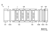
- FIG. 1 is a side view diagrammatically illustrating a printer according to a first embodiment.
- FIG. 2 is a plan view illustrating the printer according to the first embodiment.
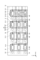
- FIG. 3 is a plan view that illustrates the liquid ejection head according to the first embodiment.
- FIG. 4 is a view of the liquid ejection head shown in FIG.
- FIG. 5 is a plan view illustrating the actuator substrate according to the first embodiment.
- FIG. 6 is a cross-sectional view taken along line II shown in FIG.
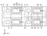
- FIG. 7 is an enlarged view of region II shown in FIG.
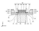
- FIG. 8 is a cross-sectional view taken along line III-III shown in FIG.
- FIG. 9 is a cross-sectional view taken along line IV-IV shown in FIG.
- FIG. 10 is a cross-sectional view illustrating an example of the configuration of the insulator according to the first embodiment.
- FIG. 11 is an enlarged view of region V shown in FIG.
- FIG. 12 is a cross-sectional view taken along line VI-VI shown in FIG.
- FIG. 13 is an enlarged cross-sectional view showing a part of the actuator substrate according to the second embodiment.
- FIG. 14 is a cross-sectional view showing an example of the configuration of a piezoelectric element according to the second embodiment.
- FIG. 15 is an enlarged cross-sectional view showing a part of the actuator substrate according to the third embodiment.
- FIG. 16 is an enlarged cross-sectional view showing a part of the actuator substrate according to the fourth embodiment.
- FIG. 17 is an enlarged cross-sectional view showing a part of the actuator substrate according to the fifth embodiment.
- the displacement of the piezoelectric element could cause compressive or tensile stress in the vibration plate, which could cause the ends of the insulator to peel off.
- FIG. 1 is a side view that shows a schematic diagram of a printer 10 including a liquid ejection head 1 according to this embodiment.
- FIG. 2 is a plan view that shows a schematic diagram of the printer 10.
- the printer 10 is, for example, a color inkjet printer.
- the printer 10 includes a paper feed roller 101, a guide roller 102, a transport roller 103, a recovery roller 104, a head case 105, a frame 106, a liquid ejection head 1, a dryer 107, a sensor unit 108, and a control unit 109.
- the control unit 109 controls the operation of the paper feed roller 101, the guide roller 102, the transport roller 103, the recovery roller 104, the head case 105, the frame 106, the liquid ejection head 1, the dryer 107, and the sensor unit 108.
- the paper feed roller 101, guide roller 102, transport roller 103, and recovery roller 104 constitute a moving section that moves the print paper P and the liquid ejection head 1 relative to one another.
- the print paper P is an example of a recording medium.
- the moving section is controlled by the control section 109.
- the print paper P passes between the paper feed roller 101, two guide rollers 102A, and is transported onto the multiple transport rollers 103.
- the print paper P then passes between two guide rollers 102B and two guide rollers 102C, and is transported to the recovery roller 104.
- the head case 105 houses the transport roller 103, the frame 106, and the liquid ejection head 1.
- the head case 105 is connected to the outside in some areas, such as the area where the printing paper P enters and exits, but the rest of the head case 105 is a space isolated from the outside.
- the control unit 109 controls factors such as temperature, humidity, and air pressure in the internal space of the head case 105 as necessary.
- the frame 106 is flat and positioned close to and above the print paper P being transported by the transport rollers 103. There are four frames 106 inside the head case 105, positioned at predetermined intervals along the transport direction of the print paper P. The number of frames 106 mounted on the printer 10 can be changed as appropriate depending on the object to be printed or the printing conditions.
- the liquid ejection head 1 has a long, narrow shape that is elongated in the vertical direction in FIG. 2. As shown in FIG. 2, five liquid ejection heads 1 are mounted on each frame 106. In each frame 106, three liquid ejection heads 1 are lined up in a direction intersecting the transport direction of the print paper P, and the other two liquid ejection heads 1 are lined up one between the three liquid ejection heads 1 at positions offset along the transport direction. In each frame 106, the liquid ejection heads 1 are arranged so that they overlap in the transport direction of the print paper P. The number of liquid ejection heads 1 included in one frame 106 can be changed as appropriate depending on the object to be printed or the printing conditions.
- the liquid ejection head 1 is fixed to the printer 10, which is a so-called line printer.
- the printer is not limited to a line printer, and may be a so-called serial printer in which the liquid ejection head 1 is moved in a direction intersecting the transport direction of the printing paper P to eject droplets and transport the printing paper P alternately.
- the liquid ejection head 1 is controlled by the control unit 109 based on data such as images or characters, and ejects liquid toward the printing paper P.
- the distance between the liquid ejection head 1 and the printing paper is, for example, about 0.5 to 20 mm.
- the liquid ejection heads 1 belonging to one frame 106 are supplied with the same color liquid, and four colors of liquid can be printed using four frames 106.
- the colors of liquid ejected from the liquid ejection heads 1 of each frame 106 are, for example, magenta, yellow, cyan, and black. By causing such liquid to land on the printing paper P, a color image can be printed. The type of liquid color can be changed as appropriate. Also, several colors of liquid can be supplied to the liquid ejection heads 1 belonging to one frame 106, and several colors of liquid can be printed using one frame 106.
- liquids such as coating agents may be printed uniformly or in a pattern using the liquid ejection head 1 to treat the surface of the printing paper P.
- the coating agent may be applied using an applicator (not shown).
- the dryer 107 dries the printing paper P. After passing through the two guide rollers 102B, the printing paper P is dried by the dryer 107. By drying in the dryer 107, the printing paper P that is wound up overlapping on the collection roller 104 is less likely to stick to each other, and the undried liquid is less likely to rub against each other.
- the sensor unit 108 includes a position sensor, a speed sensor, a temperature sensor, etc.
- the control unit 109 can control each part of the printer 10 based on information from each sensor.
- the printer 10 may be equipped with a cleaning unit that cleans the liquid ejection head 1.
- the cleaning unit cleans the liquid ejection head 1, for example, by wiping or capping.
- the recording medium may be a roll of cloth or the like.
- the printer 10 may also transport the recording medium on a transport belt. In this way, sheets of paper, cut pieces of cloth, wood, tiles, or the like can be used as recording media.
- a liquid containing conductive particles may be ejected from the liquid ejection head 1 to print wiring patterns for electronic devices, or the like.
- a chemical agent may be produced by ejecting a predetermined amount of liquid chemical agent or a liquid containing a chemical agent from the liquid ejection head 1 toward a reaction vessel or the like and causing a reaction.
- Figure 3 is a plan view that shows a schematic diagram of the liquid ejection head 1 according to this embodiment.
- Figure 4 is a side view of the liquid ejection head 1 shown in Figure 3, viewed from the direction A.
- FIG. 3 illustrates a three-dimensional Cartesian coordinate system including an X-axis with the positive direction pointing upward on the page, and a Y-axis with the positive direction pointing to the right on the page.
- This Cartesian coordinate system is also shown in other drawings used in the following explanation.
- the positive Z-axis side of the liquid ejection head 1 may be referred to as "upper".
- the X-axis direction is the transport direction of the printing paper P.
- a plan view refers to a view from the Z-axis direction
- a cross-sectional view refers to a view from the X-axis direction.
- the liquid ejection head 1 includes a nozzle substrate 2, an actuator substrate 3, a support substrate 4, a liquid supply substrate 5, a flexible substrate 6, and a drive IC 7.
- the nozzle substrate 2 has multiple nozzles 21.
- the nozzles 21 are through holes that penetrate the nozzle substrate 2 in the Z-axis direction.
- the actuator substrate 3 is located on the nozzle substrate 2. When pressure is applied to the liquid in the actuator substrate 3, the liquid is ejected from each nozzle 21 to the outside as droplets.
- the actuator substrate 3 in this embodiment has approximately the same shape as the nozzle substrate 2 in a plan view.
- the support substrate 4 is located on the actuator substrate 3.
- the support substrate 4 supplies liquid to the actuator substrate 3.
- the support substrate 4 has a predetermined thickness that is thicker in the Z-axis direction than the actuator substrate 3, and has the function of supporting the actuator substrate 3.
- the support substrate 4 according to this embodiment has a shape that is smaller than the nozzle substrate 2 and the actuator substrate 3 in a plan view.
- the liquid supply substrate 5 is located on the support substrate 4.
- the liquid supply substrate 5 supplies liquid to the support substrate 4.
- the liquid supply substrate 5 has a function of storing liquid to be supplied to the support substrate 4.
- the liquid supply substrate 5 in this embodiment has approximately the same shape as the support substrate 4 in a plan view.
- the flexible substrate 6 is located on both ends of the actuator substrate 3 in the X-axis direction.
- the liquid ejection head 1 according to this embodiment has two flexible substrates 6, but is not limited to this.
- the liquid ejection head 1 may have only one flexible substrate 6, or three or more flexible substrates 6.
- One end of the flexible substrate 6 is electrically connected to the actuator substrate 3, and the other end of the flexible substrate 6 is pulled out above the support substrate 4.
- the flexible substrate 6 is a flexible wiring substrate, and has the function of transmitting a drive signal to the actuator substrate 3.
- the driving IC 7 is mounted on the flexible substrate 6.
- the driving IC 7 is electrically connected to the control unit 109. Therefore, the driving IC 7 generates a driving signal based on a signal sent from the control unit 109. Furthermore, the driving IC 7 outputs this driving signal to the actuator substrate 3 via the flexible substrate 6. This allows the driving IC 7 to control the driving of the liquid ejection head 1.
- Figs. 3 and 4 show an example of the configuration of the liquid ejection head 1, and the liquid ejection head 1 may further include components other than those shown in Figs. 3 and 4.
- Figure 5 is a plan view showing the actuator substrate 3 in a schematic manner.
- Figure 6 is a cross-sectional view taken along line II shown in Figure 5.
- the actuator substrate 3 according to this embodiment actually has a shape in which the length in the Y-axis direction is longer than the length in the X-axis direction as shown in Figure 3, but for ease of explanation, Figure 5 shows the shape in which the length in the X-axis direction is longer than the length in the Y-axis direction.
- Figure 6 also shows the nozzle substrate 2, support substrate 4, and liquid supply substrate 5.
- the actuator substrate 3 has a pressure chamber 31, a liquid chamber 32, a solid body 33, a vibration plate 34, a piezoelectric element 35, an electrical junction 36, a first lead-out wiring 37, a wiring 38, a second lead-out wiring 39, an insulator 3N, and a protective film 3P.
- Each pressure chamber 31 is provided so as to communicate with each nozzle 21 in the nozzle substrate 2.
- a plurality of pressure chambers 31 are provided along the row direction.
- a plurality of pressure chambers 31 provided along the row direction form one pressure chamber group 311.
- Eight pressure chamber groups 311 according to this embodiment are formed in the X-axis direction. The number of pressure chamber groups 311 formed in the X-axis direction can be changed as appropriate.
- Each pressure chamber group 311 has two first pressure chambers 312, which are pressure chambers located at both ends in the Y-axis direction. In a plan view, the pressure chambers 31 are positioned so that their longitudinal direction is along the X-axis direction.
- the pressure chambers 31 according to this embodiment have a substantially rectangular planar shape, but are not limited to this.
- the pressure chambers 31 may have a diamond or circular planar shape.
- liquid is stored in the pressure chambers 31.
- the liquid chamber 32 is connected to one end of each pressure chamber 31 in the longitudinal direction.
- the liquid chamber 32 is connected to the end of each pressure chamber 31 on the negative side of the X-axis, and in the four pressure chamber groups 311 on the negative side of the X-axis, the liquid chamber 32 is connected to the end of each pressure chamber 31 on the positive side of the X-axis.
- each liquid chamber 32 and each pressure chamber 31 correspond one-to-one, and form one hollow area 3A in the actuator substrate 3. Liquid is stored in the liquid chamber 32.
- Each liquid chamber 32 is supplied with liquid from a common flow path 51 of the liquid supply substrate 5 via a connection flow path 41 in the support substrate 4.
- the common flow path 51 is provided in common to each pressure chamber group 311.
- the liquid chamber 32 according to this embodiment is connected to only one end of the pressure chamber 31 in the longitudinal direction, but may be connected to both ends of the pressure chamber 31 in the longitudinal direction.
- one liquid chamber 32 is supplied with liquid from a first common flow path in the liquid supply substrate 5, and the other liquid chamber 32 discharges liquid to a second common flow path.
- This provides the liquid ejection head 1 with a circulation function.
- the liquid chambers 32 may have a width smaller than that of the pressure chambers 31. When the liquid chambers 32 have a width smaller than that of the pressure chambers 31, the liquid chambers 32 function as throttles.
- the solid 33 is located around each hollow region 3A and has the function of separating each hollow region 3A from the other hollow regions 3A.
- the solid 33 has a partition 331 and a wall portion 332.
- the partition 331 is a portion of the solid 33 located between the pressure chamber 31 and the adjacent pressure chamber 31. In other words, the partition 331 is a portion of the solid 33 located between the pressure chambers 31.
- the wall portion 332 is a portion of the solid 33 located on the opposite side of the partition 331 from the first pressure chamber 312. In other words, the first pressure chamber 312 is located next to one side of the wall portion 332, but the pressure chamber 31 is not located next to the other side of the wall portion 332. Examples of materials that make up the solid 33 include Si.
- the vibration plate 34 is provided on the pressure chamber 31, the liquid chamber 32, and the solid body 33.
- the vibration plate 34 has an opening 341 in a part corresponding to each liquid chamber 32. Liquid is supplied to the liquid chamber 32 from the connection flow path 41 in the liquid supply substrate 5 through the opening 341.
- the thickness of the vibration plate 34 may be, for example, 1 ⁇ m or more and 10 ⁇ m or less.
- the vibration plate 34 according to this embodiment is a single layer, but is not limited to this.
- the vibration plate 34 may have a multi-layer structure.
- the vibration plate 34 may also have a multi-layer structure locally, for example, only on the solid portion 33.
- the thickness of the vibration plate 34 on the solid portion 33 may be thicker than the thickness of the vibration plate 34 on the pressure chamber 31.
- Examples of materials that can be used for the vibration plate 34 include SiO 2 and Si.
- the piezoelectric element 35 is provided on the vibration plate 34 corresponding to the pressure chamber 31.
- the piezoelectric element 35 is provided in a 1:1 relationship with the pressure chamber 31.
- the piezoelectric element 35 is composed of a common electrode 351, a piezoelectric body 352, and an individual electrode 353.
- the common electrode 351 is located on the vibration plate 34 corresponding to the pressure chamber 31
- the piezoelectric body 352 is located on the common electrode 351
- the individual electrode 353 is located on the piezoelectric body 352, but this is not limited to this.
- the order of the common electrode 351 and the individual electrode 353 from the vibration plate 34 may be reversed.
- the individual electrode 353, the piezoelectric body 352, and the common electrode 351 may be provided on the vibration plate 34 in this order.
- the common electrode 351 is provided across multiple pressure chambers 31 for each pressure chamber group 311 in plan view, but is not limited to this.
- the common electrode 351 may be provided across multiple pressure chamber groups 311, or may be provided individually corresponding to each pressure chamber 31.
- the thickness of the common electrode 351 may be 0.05 ⁇ m or more and 1 ⁇ m or less.
- materials constituting the common electrode 351 include metal materials such as Pt.
- the piezoelectric body 352 is provided individually corresponding to each pressure chamber 31, but is not limited thereto.
- the piezoelectric body 352 may be provided across a plurality of pressure chambers 31 in a plan view.
- a portion sandwiched between the individual electrode 353 and the common electrode 351 is polarized in the thickness direction in the Z-axis direction. Therefore, for example, when a voltage is applied in the polarization direction of the piezoelectric body 352 by the individual electrode 353 and the common electrode 351, the piezoelectric body 352 contracts in a direction along the vibration plate 34. This contraction is regulated by the vibration plate 34.
- the piezoelectric body 352 is displaced so as to be convex toward the pressure chamber 31 side. With the displacement of the piezoelectric body 352, the vibration plate 34 located above the pressure chamber 31 is also displaced. As a result, pressure is applied to the liquid in the pressure chamber 31.
- the thickness of the piezoelectric body 352 may be 1 ⁇ m or more and 10 ⁇ m or less. Examples of the constituent material of the piezoelectric body 352 include ferroelectric ceramic materials such as Pb(Zr, Ti) O3- based, NaNbO3- based, BaTiO3- based, (BiNa) NbO3- based, and BiNaNB5O15 - based.
- the individual electrodes 353 are provided individually corresponding to each pressure chamber 31.
- the thickness of the individual electrodes 353 may be 0.05 ⁇ m or more and 1 ⁇ m or less.
- the constituent material of the individual electrodes 353 may be, for example, a metal material such as Pt.
- the electrical joints 36 are located on both ends of the diaphragm 34 in the X-axis direction.
- the electrical joints 36 are formed of multiple terminals.
- the multiple terminals are electrically connected to the flexible substrate 6.
- the first outgoing wiring 37 is electrically connected to the individual electrodes 353 and is wiring that is drawn out from each individual electrode 353. In a plan view, the first outgoing wiring 37 is drawn out from a portion corresponding to the pressure chamber 31 to a portion corresponding to the solid portion 33.
- the thickness of the first outgoing wiring 37 may be, for example, 0.1 ⁇ m or more and 1 ⁇ m or less. Examples of materials that make up the first outgoing wiring 37 include Au.
- the wiring 38 is located on the vibration plate 34 and is electrically connected to the first lead-out wiring 37.
- the wiring 38 is led out from the connection point with the first lead-out wiring 37 to the electrical joint 36 and is electrically connected to the terminal of the electrical joint 36.
- the wiring 38 is connected to the first lead-out wiring 37 corresponding to the piezoelectric elements 35 of the four rows of pressure chamber groups 311 located on the positive side of the X-axis, it is led out to the electrical joint 36 located on the positive side of the X-axis, and when the wiring 38 is connected to the first lead-out wiring 37 corresponding to the piezoelectric elements 35 of the four rows of pressure chamber groups 311 located on the negative side of the X-axis, it is led out to the electrical joint 36 located on the negative side of the X-axis.
- the thickness of the wiring 38 may be, for example, 0.1 ⁇ m or more and 1 ⁇ m or less. Examples of materials that make up the wiring 38 include AlCu and Au.
- the second lead-out wiring 39 is led from the common electrode 351 corresponding to each piezoelectric element 35 to the electrical joint 36 and is electrically connected to the terminal of the electrical joint 36.
- a ground potential is applied to the common electrode 351 from the flexible substrate 6 via the electrical joint 36 and the second lead-out wiring 39. Note that the ground potential means 0V.
- the second lead-out wiring 39 is arranged so as to surround each pressure chamber group 311 in a plan view.
- the thickness of the second lead-out wiring 39 may be, for example, 0.1 ⁇ m or more and 1 ⁇ m or less. Examples of materials for the second lead-out wiring 39 include AlCu and Au.
- the insulator 3N is provided on the vibration plate 34 so as to cover the wiring 38 in order to reduce the possibility of the wiring 38 corroding.
- the insulator 3N is generally in close contact with the vibration plate 34 corresponding to the portion excluding the pressure chamber 31. That is, the insulator 3N is generally in close contact with the vibration plate 34 corresponding to the liquid chamber 32 and the solid portion 33.
- the insulator 3N according to this embodiment is in close contact with the vibration plate 34 and the wiring 38 by using the CVD method. By using the CVD method, the step coverage is improved, so that the insulator 3N has high coverage with respect to the wiring 38, and the possibility of the wiring 38 corroding can be further reduced.
- the CVD method is used as the method for adhering the insulator 3N according to this embodiment, but is not limited thereto.
- the insulator 3N may be in close contact with the vibration plate 34 and the wiring 38 by using the sputtering method. By using the sputtering method, particles that are the constituent material of the insulator 3N are attached to the vibration plate 34 and the wiring 38 with high energy. This increases the adhesion between the insulator 3N and the diaphragm 34 and the wiring 38.
- the thickness of the insulator 3N may be set to, for example, 0.01 ⁇ m or more and 1 ⁇ m or less.
- the material of the insulator 3N may be, for example, SiO 2 .
- the protective film 3P is located on the insulator 3N and the piezoelectric element 35.
- the thickness of the protective film 3P may be, for example, 0.01 ⁇ m or more and 1 ⁇ m or less. Note that the protective film 3P is not shown in Fig. 5.
- the first escape wiring 37 and the second escape wiring 39 are located on the insulator 3N, but in reality, they are located on the protective film 3P. Examples of materials that make up the protective film 3P include Al2O3 , SiO2 , and SiN.
- FIG. 7 is an enlarged view of region II shown in FIG. 5. Note that the second exit wiring 39 and protective film 3P are omitted from FIG. 7.
- the wiring 38 is located on the first region 342 and the second region 343.
- the first region 342 is the region on the vibration plate 34 that corresponds to the partition wall 331.
- the second region 343 is the region that corresponds to the portion of the region other than the first region 342 excluding the pressure chamber 31.
- the number of wirings 38 located on the first region 342 varies depending on the pressure chamber group 311.
- the pressure chamber groups 311 are, from the positive X-axis direction side, the first pressure chamber group 3111, the second pressure chamber group 3112, the third pressure chamber group 3113, and the fourth pressure chamber group 3114.
- Three wirings 38 are located on the first region 342 of the first pressure chamber group 3111.
- Two wirings 38 are located on the first region 342 of the second pressure chamber group 3112.
- One wiring 38 is located on the first region 342 of the third pressure chamber group 3113.
- No wiring 38 is located on the first region 342 of the fourth pressure chamber group 3114.
- the number of wirings 38 on each first region 342 may be set appropriately.
- the wirings 38 are located on the first region 342 and the second region 343, but this is not limited to this.
- the second outgoing wiring 39 may be located on the first region 342 and the second region 343, in which case a configuration similar to that of the wiring 38 described above may be adopted.
- Figure 8 is a cross-sectional view taken along line III-III in Figure 7.
- Figure 9 is a cross-sectional view taken along line IV-IV in Figure 7.
- the protective film 3P is omitted from Figures 8 and 9.
- the insulator 3N covering the wiring 38 located on the first region 342 has one end 3N1 at the end on the positive side of the Y axis and the other end 3N2 at the end on the negative side of the Y axis. In other words, the insulator 3N covering the wiring 38 located on the first region 342 has one end 3N1 and the other end 3N2 at the ends in the width direction.
- the common electrode 351 is provided from the surface of the insulator 3N at one end 3N1 to the surface of the other end 3N2. In other words, the common electrode 351 is provided so as to cover the insulator 3N.
- it is sufficient that the common electrode 351 is provided so as to cover the insulator 3N covering the wiring 38 located on the first region 342 at least when viewed in cross section.
- the piezoelectric body 352 When a voltage is applied to the piezoelectric body 352 by the individual electrode 353 and the common electrode 351, the piezoelectric body 352 is displaced. Since the piezoelectric element 35 is located on the vibration plate 34 corresponding to the pressure chamber 31, the vibration plate 34 located on this pressure chamber 31 is also displaced in accordance with the displacement of the piezoelectric body 352. Furthermore, since the vibration plate 34 located on the partition wall 331 is supported by the partition wall 331, when the vibration plate 34 located on the pressure chamber 31 is displaced, a compressive stress or tensile stress is generated in the vibration plate 34. Furthermore, a compressive stress or tensile stress is generated at the interface between the vibration plate 34 and the insulator 3N. Therefore, the insulator 3N is easily peeled off from the vibration plate 34.
- the common electrode 351 is provided across the surface of the insulator 3N at one end 3N1 to the surface of the other end 3N2. This allows the common electrode 351 to press down on the one end 3N1 and the other end 3N2 of the insulator 3N, as well as the central portion 3N3 of the insulator 3N. This reduces the possibility that the insulator 3N will peel off from the vibration plate 34.
- the common electrode 351 is provided from the surface at one end 3N1 of the insulator 3N to the surface at the other end 3N2, the common electrode 351 is longer and the area of the common electrode 351 is larger than when the common electrode 351 is provided at the interface between the vibration plate 34 and the insulator 3N as in Patent Document 1. Since the area of the common electrode 351 is larger, the resistance value of the common electrode 351 is smaller. Since the resistance value of the common electrode 351 is smaller, it is possible to suppress the rounding of the waveform of the voltage applied to the piezoelectric body 352 via the common electrode 351.
- the liquid ejection head 1 in the liquid ejection head 1 according to this embodiment, it is possible to suppress the rounding of the waveform, and therefore it is possible to reduce the variation in the waveform applied to the piezoelectric body 352. Therefore, in the liquid ejection head 1 according to this embodiment, it is possible to reduce the variation in the ejection of the liquid.
- the common electrode 351 is provided from the surface at one end 3N1 of the insulator 3N to the surface at the other end 3N2, so that it is possible to reduce the possibility of moisture or ink adhering to the surface of the insulator 3N and penetrating into the insulator 3N. Since it is possible to reduce the possibility of moisture or ink penetrating into the insulator 3N, it is possible to reduce the possibility of moisture or ink reaching the wiring 38. Therefore, in the liquid ejection head 1 according to this embodiment, it is possible to further reduce the possibility of the wiring 38 corroding.
- the liquid ejection head 1 As described above, three wires 38 are located on the first region 342 of the first pressure chamber group 3111. Two wires 38 are located on the first region 342 of the second pressure chamber group 3112. In other words, the liquid ejection head 1 according to this embodiment has locations on the first region 342 where multiple wires 38 are arranged side by side.
- the liquid ejection head 1 there are locations on the first region 342 where multiple wirings 38 are arranged side by side, and an electric field is generated between the wirings 38 at these locations. If moisture or ink were to get inside the insulator 3N, the moisture or ink could move in the direction of the electric field generated between the wirings 38, potentially causing the insulator 3N to break down. If the insulator 3N breaks down, moisture or ink could get between the wirings 38, potentially causing a short circuit between the wirings 38.
- the common electrode 351 is provided from the surface at one end 3N1 of the insulator 3N to the surface at the other end 3N2. Therefore, in the liquid ejection head 1 according to this embodiment, the possibility of moisture or ink penetrating into the insulator 3N can be reduced, and therefore the possibility of moisture or ink reaching between the wirings 38 can be reduced. Therefore, in the liquid ejection head 1 according to this embodiment, the possibility of short-circuiting between the wirings 38 can be reduced.
- the insulator 3N is composed of a first portion 3N4 and a second portion 3N5.
- the second portion 3N5 is thinner in the Z-axis direction than the first portion 3N4.
- the second portion 3N5 includes one end 3N1 and the other end 3N2. That is, in FIG. 8, the insulator 3N has the second portions 3N5 provided on the Y-axis positive side and the Y-axis negative side of the first portion 3N4.
- residual stress may occur in the insulator 3N due to the process of forming the insulator 3N.
- the residual stress occurring in the insulator 3N may cause one end 3N1 and the other end 3N2 of the insulator 3N to peel off from the vibration plate 34.
- the thickness of the second portion 3N5 including the one end 3N1 and the other end 3N2 is thinner in the Z-axis direction than the first portion 3N4, so it is possible to reduce the residual stress occurring in the one end 3N1 and the other end 3N2 of the insulator 3N. Therefore, in the liquid ejection head 1 according to this embodiment, it is possible to reduce the possibility that the one end 3N1 and the other end 3N2 of the insulator 3N will peel off from the vibration plate 34.
- the thickness of the second portion 3N5 in this embodiment in the Z-axis direction is thinner than the thickness of the wiring 38 in the Z-axis direction. Since the thickness of the second portion 3N5 is thinner than the thickness of the wiring 38, the residual stress generated at one end 3N1 and the other end 3N2 of the insulator 3N can be further reduced.
- the thickness of the second portion 3N5 in this embodiment is thinner than the thickness of the wiring 38, but is not limited to this.
- the thickness of the second portion 3N5 may be thinner than the thickness of the first portion 3N4 and thicker than the thickness of the wiring 38, for example.
- the step portion 3S formed by the first portion 3N4 and the second portion 3N5 is provided at a position higher than the upper surface of the wiring 38 in the Z-axis direction. Since moisture or ink is likely to accumulate in this step portion 3S, moisture or ink is likely to enter the inside of the insulator 3N from this step portion 3S. Since this step portion 3S is provided at a position higher than the upper surface of the wiring 38 in the Z-axis direction, the distance between the wiring 38 and this step portion 3S is longer. Because the distance between the wiring 38 and the step portion 3S is longer, the possibility that moisture or ink that has penetrated into the insulator 3N will reach the wiring 38 can be reduced. Therefore, in such a liquid ejection head 1, the possibility that the wiring 38 will corrode can be reduced.
- the second portion 3N5 in this embodiment is provided from the top of the vibration plate 34 corresponding to the partition wall 331 to the top of the vibration plate 34 corresponding to the pressure chamber 31.
- the pressure chambers 31 are formed by etching, but side etching may occur at the boundary of the partition 331 where it contacts the pressure chamber 31 and at a location 313 where it also contacts the vibration plate 34. This causes side etching to cause this location 313 to vary for each pressure chamber 31. In other words, this causes variation in the displacement of the vibration plate 34.
- the second portion 3N5 is located on the vibration plate 34 corresponding to the pressure chamber 31, so the displacement of the vibration plate 34 where the second portion 3N5 is located is suppressed. In other words, in the liquid ejection head 1 according to this embodiment, it is possible to define the location of the vibration plate 34 that is displaced by the second portion 3N5, and the variation in the displacement of the vibration plate 34 can be suppressed.
- the length 3L in the Y-axis direction of the portion of the second portion 3N5 that corresponds to the pressure chamber 31 is uniform in all of the pressure chambers 31. This makes it possible to uniformly define the location of displacement of the vibration plate 34 for all pressure chambers 31, and to reduce variation in the displacement of the vibration plate 34 for each pressure chamber 31. Note that "uniform” here does not mean completely uniform, but rather means that manufacturing errors and the like are tolerated.
- the length 3L in the Y-axis direction of the portion of the second portion 3N5 that corresponds to the pressure chamber 31 is uniform, but this is not limited to this.
- the length 3L in the Y-axis direction of the portion of the second portion 3N5 that corresponds to the pressure chamber 31 may be changed for each pressure chamber 31 to specify the location of displacement of the vibration plate 34.
- the second portion 3N5 is provided from the diaphragm 34 corresponding to the partition 331 to the diaphragm 34 corresponding to the pressure chamber 31, but this is not limiting.
- the second portion 3N5 may be configured to be located only on the diaphragm 34 corresponding to the partition 331, and not on the diaphragm 34 corresponding to the pressure chamber 31.
- the second portion 3N5 is not located on the vibration plate 34 corresponding to the pressure chamber 31, so the second portion 3N5 does not hinder the displacement of the vibration plate 34 corresponding to the pressure chamber 31. Therefore, in such a liquid ejection head 1, the possibility of a decrease in the amount of liquid ejected can be reduced compared to when the second portion 3N5 is located on the vibration plate 34 corresponding to the pressure chamber 31.
- the insulator 3N may be composed of only the first portion 3N4.
- the cross-sectional shape of the insulator 3N may be semicircular.
- the surface of the insulator 3N forms a convex curved surface.
- the compressive stress or tensile stress generated in the insulator 3N can be alleviated by the convex curved surface.
- the common electrode 351 is provided on the convex curved surface, it is possible to make the thickness of the common electrode 351 uniform, and the possibility of the common electrode 351 being broken can be reduced.
- the common electrode 351 is located between the piezoelectric body 352 and the wiring 38. Also, as described above, the common electrode 351 is set to the ground potential.
- the piezoelectric body 352 is displaced by the application of a voltage.
- the electric field generated from the wiring 38 may affect the voltage applied to the piezoelectric body 352, and thus affect the liquid ejection characteristics.
- the common electrode 351 is located between the piezoelectric body 352 and the wiring 38 in a cross-sectional view, so that the common electrode 351, which is set to ground potential, can shield the electric field generated from the wiring 38 from reaching the piezoelectric body 352. Therefore, in the liquid ejection head 1 according to this embodiment, it is possible to reduce the possibility of affecting the liquid ejection characteristics.
- FIG. 11 is an enlarged view of region V shown in FIG. 7. Note that the second exit wiring 39 and protective film 3P are omitted from FIG. 11.
- the insulator 3N covers the wiring 38 in the first region 342 and is in close contact with the vibration plate 34, and also covers the wiring 38 in the second region 343 and is in close contact with the vibration plate 34.
- the width W2 of the insulator 3N located on the second region 343 is larger than the width W1 of the insulator 3N located on the first region 342.
- the width of the insulator 3N refers to the width of the insulator 3N in the Y-axis direction. Therefore, the width W1 of the insulator 3N located on the first region 342 is the distance from one end 3N1 to the other end 3N2 of the insulator 3N. Since the insulator 3N according to this embodiment is generally located on the vibration plate 34 corresponding to the portion excluding the pressure chamber 31, the width W2 of the insulator 3N located on the second region 343 is the distance between the adjacent openings 341.
- width W1 of the insulator 3N located on the first region 342 is made larger than the width W2 of the insulator 3N located on the second region 343, one end 3N1 and the other end 3N2 of the insulator 3N located on the first region 342 will be closer to the piezoelectric body 352, and will be susceptible to the compressive stress or tensile stress caused by the displacement of the vibration plate 34.
- the width W2 of the insulator 3N located on the second region 343 is greater than the width W2 of the insulator 3N located on the first region 342.
- one end 3N1 and the other end 3N2 of the insulator 3N located on the first region 342 do not approach the piezoelectric body 352. Therefore, in the liquid ejection head 1 according to the embodiment, one end 3N1 and the other end 3N2 of the insulator 3N located on the first region 342 are less susceptible to the effects of compressive stress or tensile stress generated in the vibration plate 34.
- the width W2 of the insulator 3N located on the second region 343 is greater than the width W1 of the insulator 3N located on the first region 342, the contact area between the insulator 3N located on the second region 343 and the diaphragm 34 is large. This increases the adhesion between the insulator 3N located on the second region 343 and the diaphragm 34, reducing the possibility of the insulator 3N peeling off from the diaphragm 34.
- the insulator 3N is positioned on the diaphragm 34 so as to surround the opening 341.
- a pressure wave is generated in the pressure chamber 31 due to the displacement of the piezoelectric body 352, but since the liquid chamber 32 is connected to the pressure chamber 31, the pressure wave generated in the pressure chamber 31 propagates to the liquid chamber 32.
- the pressure wave propagated to the liquid chamber 32 also propagates to the common flow path 51 through the opening 341.
- the pressure wave propagated to the common flow path 51 also propagates to the adjacent pressure chamber 31 via this common flow path 51, affecting the ejection characteristics of the adjacent pressure chamber 31.
- so-called fluid crosstalk occurs, in which the adjacent pressure chambers 31 affect each other in terms of the ejection characteristics of the liquid.
- the insulator 3N surrounds the opening 341 and is also located on the vibration plate 34 corresponding to the liquid chamber 32, so that the displacement of the vibration plate 34 corresponding to the liquid chamber 32 can be suppressed. Therefore, in the liquid ejection head 1 according to the embodiment, it is possible to attenuate the pressure waves propagating from the liquid chamber 32 to the common flow path 51 through the opening 341, thereby reducing fluid crosstalk.
- the wall portion 332 is the portion of the solid body 33 that is located on the opposite side of the partition wall 331 from the first pressure chamber 312.
- the first pressure chamber 312 refers to the two pressure chambers located at both ends in the Y-axis direction in each pressure chamber group 311.
- FIG. 12 is a cross-sectional view taken along line VI-VI shown in FIG. 7. The protective film 3P is omitted from FIG. 12.
- the insulator 3N according to this embodiment is also provided on the diaphragm 34 corresponding to the wall portion 332.
- the thickness of the insulator 3N on the diaphragm 34 corresponding to the wall portion 332 is approximately equal to the thickness of the first portion 3N4 of the insulator 3N on the diaphragm 34 corresponding to the partition wall 331.
- the common electrode 351 is not provided on the insulator 3N on the diaphragm 34 corresponding to the wall portion 332.
- the pressure chambers 31 other than the first pressure chamber 312 have partitions 331 on both sides in the row direction. Therefore, these pressure chambers 31 have insulators 3N on both sides in the row direction.
- the first pressure chamber 312 has a partition 331 on one side in the row direction and a wall portion 332 on the other side in the row direction.
- the vibration plate 34 corresponding to the first pressure chamber 312 will be displaced in the row direction as compared to the pressure chambers 31 other than the first pressure chamber 312. Therefore, there is a possibility that the liquid ejection variation will occur in the first pressure chamber 312.
- the insulator 3N is also provided on the vibration plate 34 corresponding to the wall portion 332, so that the vibration plate 34 corresponding to the first pressure chamber 312 can reduce the possibility of displacement bias occurring in the row direction. Therefore, in the liquid ejection head 1 according to the embodiment, the possibility of liquid ejection variation occurring can be reduced.
- the common electrode 351 according to the embodiment is not provided on the insulator 3N corresponding to the wall portion 332, this is not limiting.
- the common electrode 351 may also be provided on the insulator 3N corresponding to the wall portion 332.
- the first pressure chamber 312 has the common electrode 351 on both sides in the row direction, similar to the pressure chambers 31 other than the first pressure chamber 312. Therefore, the vibration plate 34 corresponding to the first pressure chamber 312 can reduce the possibility of displacement bias occurring in the row direction. Therefore, the liquid ejection head 1 according to this embodiment can further reduce the possibility of liquid ejection variation occurring.
- the nozzle substrate 2, actuator substrate 3, support substrate 4, liquid supply substrate 5, flexible substrate 6, and drive IC 7 are prepared. Then, the actuator substrate 3 is bonded onto the nozzle substrate 2, and the support substrate 4 is bonded onto the actuator substrate 3. Then, the liquid supply substrate 5 is bonded onto the support substrate 4. Then, the flexible substrate 6 on which the drive IC 7 is mounted is bonded to the electrical joint 36 of the actuator substrate 3. In this way, the liquid ejection head 1 can be manufactured.
- methods for bonding the substrates include a method of bonding them by applying pressure while heating under a vacuum. Examples of methods for bonding the actuator substrate 3 and the flexible substrate 6 include a method of bonding them by using an adhesive.
- liquid supply substrate 5 is bonded onto the support substrate 4, and then the flexible substrate 6 is bonded to the electrical joint 36 of the actuator substrate 3, but this is not limiting.
- the liquid supply substrate 5 may be bonded onto the support substrate 4 after the flexible substrate 6 is bonded to the electrical joint 36 of the actuator substrate 3. In other words, there is no limitation on the order of bonding.
- the actuator substrate 3 can be manufactured by sequentially depositing and etching various films on a silicon wafer.
- the diaphragm 34 is formed by forming a SiO 2 film on the surface of a silicon wafer by, for example, a plasma CVD method.
- the wiring 38 is formed on the diaphragm 34 by, for example, forming a film of AlCu by sputtering, and then etching to remove unnecessary portions.
- the insulator 3N is formed on the vibration plate 34 and the wiring 38 by, for example, forming a film of SiO 2 by a CVD method, and then etching to remove unnecessary portions.
- the second portion 3N5 is formed by further etching from the vibration plate 34 corresponding to the partition wall 331 to the vibration plate 34 corresponding to the pressure chamber 31 so that the thickness is thinner than the wiring 38.
- the first portion 3N4 may be formed by further forming and etching the SiO 2 at a predetermined location so that the thickness is thicker.
- the CVD method is used as a method for forming the insulator 3N according to this embodiment, but the method is not limited to this.
- the insulator 3N may be formed on the vibration plate 34 and the wiring 38 by, for example, a sputtering method.
- the insulator 3N may be formed by stacking a plurality of insulating layers to increase the adhesion between the vibration plate 34 and the wiring 38.
- the common electrode 351 is formed on the vibration plate 34 and the insulator 3N by, for example, forming a Pt film by sputtering and then removing unnecessary portions by etching. At this time, in order to increase the adhesion between the common electrode 351 and the insulator 3N, for example, a TiO2 layer may be provided as an adhesion layer between the common electrode 351 and the insulator 3N.
- the piezoelectric body 352 is formed on the common electrode 351 by, for example, forming a film of Pb(Zr,Ti) O3 by sputtering, and then removing unnecessary portions by etching.
- the sputtering method is used as a method for forming the piezoelectric body 352 according to this embodiment, the method is not limited to this.
- the piezoelectric body 352 may be formed on the common electrode 351 by, for example, a sol-gel method.
- the individual electrodes 353 are formed on the piezoelectric body 352 by, for example, forming a Pt film by sputtering, and then etching to remove unnecessary portions.
- the protective film 3P is formed on the insulator 3N and the piezoelectric element 35 by, for example, forming a film of Al 2 O 3 by CVD and then removing unnecessary portions by etching.
- the first and second outgoing wiring 37 and 39 are formed on the protective film 3P by, for example, forming a film of Au by sputtering, and then etching to remove unnecessary portions.
- a Ti layer or a TiW layer may be provided as an adhesion layer between the first and second outgoing wiring 37 and 39 and the protective film 3P.
- the electrical junction 36 is formed by providing a plurality of terminals on the diaphragm 34 that electrically connect the wiring 38 and the second outgoing wiring 39.
- the pressure chamber 31 and the liquid chamber 32 are formed, for example, by etching a silicon wafer.
- the actuator substrate 3 is manufactured.
- the solid portion 33 is the portion of the silicon wafer that remains after etching.
- a liquid ejection head 1a according to a second embodiment will be described.
- the description of the liquid ejection head 1a according to this embodiment basically, only the differences from the liquid ejection head 1 according to the first embodiment will be described. Matters that are not specifically mentioned may be the same as those in the first embodiment or may be inferred from the first embodiment. The same applies to the third to fifth embodiments described below.
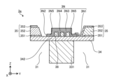
- FIG. 13 is an enlarged cross-sectional view showing a portion of the actuator substrate 3a according to this embodiment, and corresponds to FIG. 8 of the first embodiment.
- the common electrode 351 is provided from the vibration plate 34 corresponding to the pressure chamber 31 to the surface at one end 3N1 of the insulator 3N. That is, unlike the actuator substrate 3 according to the first embodiment, the common electrode 351 in the actuator substrate 3a according to this embodiment is not provided so as to cover the entire insulator 3N, but is provided so as to cover only one end 3N1 of the insulator 3N. That is, the common electrode 351 according to this embodiment is not provided in the central portion 3N3 or the other end 3N2 of the insulator 3N.
- a compressive stress or tensile stress is generated in the vibration plate 34.
- a compressive stress or tensile stress is generated at the interface between the vibration plate 34 and the insulator 3N.
- the interface between one end 3N1 of the insulator 3N and the vibration plate 34 is located closer to the piezoelectric body 352 than the central portion 3N3 of the insulator 3N, and is therefore more susceptible to the compressive stress or tensile stress generated in the vibration plate 34. For this reason, one end 3N1 of the insulator 3N is more likely to peel off from the vibration plate 34 than the central portion 3N3.
- the common electrode 351 is provided from a position corresponding to the pressure chamber 31 over the surface of one end 3N1 of the insulator 3N.
- the common electrode 351 is provided from the vibration plate 34 corresponding to the pressure chamber 31 over the surface of one end 3N1 of the insulator 3N. Because the common electrode 351 is provided on the surface of one end 3N1 of the insulator 3N, it is possible for the common electrode 351 to hold down one end 3N1 of the insulator 3N. This reduces the possibility that one end 3N1 of the insulator 3N will peel off from the vibration plate 34.
- the common electrode 351 is provided over the vibration plate 34 corresponding to the pressure chamber 31 and over the surface of one end 3N1 of the insulator 3N, but this is not limiting.
- the common electrode 351 may be provided over the vibration plate 34 corresponding to the pressure chamber 31 and over the surface of the other end 3N2 of the insulator 3N. That is, the common electrode 351 may be provided so as to cover only the other end 3N2 of the insulator 3N. That is, the common electrode 351 is not provided on one end 3N1 of the insulator 3N. In this case, the common electrode 351 can hold down the other end 3N2 of the insulator 3N, so that the possibility of the other end 3N2 of the insulator 3N peeling off from the vibration plate 34 can be reduced.
- the common electrode 351, the piezoelectric body 352, and the individual electrode 353 are provided in this order on the vibration plate 34.
- the common electrode 351 is located on the lower surface of the piezoelectric body 352.
- the common electrode 351 is not located on the side of the piezoelectric body 352.
- the side of the piezoelectric body 352 refers to the side in the Y-axis direction.
- the common electrode 351 is not located on the side of the piezoelectric body 352, so that it is possible to reduce the possibility that the common electrode 351 will hinder the displacement of the piezoelectric body 352. Since it is possible to reduce the possibility of hindering the displacement of the piezoelectric body 352, the liquid ejection head 1a according to this embodiment can reduce the possibility of the displacement of the vibration plate 34 decreasing. Therefore, in the liquid ejection head 1a according to this embodiment, it is possible to reduce the possibility of the liquid ejection amount decreasing.
- the piezoelectric element 35 may be provided on the vibration plate 34 in the order of individual electrodes 353, piezoelectric body 352, and common electrode 351, as shown in FIG. 14.
- the common electrode 351 is provided from the position corresponding to the pressure chamber 31 to the surface of one end 3N1 of the insulator 3N.
- the common electrode 351 is provided from the piezoelectric body 352 corresponding to the pressure chamber 31 to the surface of one end 3N1 of the insulator 3N, via the vibration plate 34.
- the common electrode 351 Since the common electrode 351 is provided from the piezoelectric body 352 corresponding to the pressure chamber 31 to the surface of one end 3N1 of the insulator 3N, the common electrode 351 covers not only the upper surface of the piezoelectric body 352 but also the side surface of the piezoelectric body 352. Since the common electrode 351 covers the side surface of the piezoelectric body 352, the area of the common electrode 351 is increased. Since the area of the common electrode 351 is increased, the resistance value of the common electrode 351 is reduced. Since the resistance value of the common electrode 351 is small, it is possible to suppress the distortion of the waveform of the voltage applied to the piezoelectric body 352 via the common electrode 351.
- the common electrode 351 is provided from a position corresponding to the pressure chamber 31 over the surface at one end 3N1 of the insulator 3N, but this is not limiting.
- the common electrode 351 may be provided from a position corresponding to the pressure chamber 31 over the surface at the other end 3N2 of the insulator 3N, or may be provided from the surface at one end 3N1 of the insulator 3N over the surface at the other end 3N2.
- Fig. 15 is an enlarged cross-sectional view showing a part of an actuator substrate 3b according to this embodiment, and corresponds to Fig. 8 of the first embodiment.
- the common electrode 351 is provided on the surface of one end 3N1 of the insulator 3N, and is also provided on the surface of the other end 3N2 of the insulator 3N. That is, unlike the actuator substrate 3 according to the first embodiment, the common electrode 351 in the actuator substrate 3b according to this embodiment is not provided so as to cover the entire insulator 3N, but is provided so as to cover only one end 3N1 and the other end 3N2 of the insulator 3N. That is, the common electrode 351 according to this embodiment is not provided in the central portion 3N3 of the insulator 3N.
- the interface between one end 3N1 of the insulator 3N and the diaphragm 34, and the interface between the other end 3N2 of the insulator 3N and the diaphragm 34 are both located closer to the piezoelectric body 352 than the central portion 3N3 of the insulator 3N, and are therefore more susceptible to the compressive stress or tensile stress generated in the diaphragm 34. For this reason, one end 3N1 and the other end 3N2 of the insulator 3N are more likely to peel off from the diaphragm 34 than the central portion 3N3.
- the common electrode 351 is provided on the surface of the insulator 3N at one end 3N1, and also on the surface of the insulator 3N at the other end 3N2. Since the common electrode 351 is provided not only on the surface of the insulator 3N at one end 3N1 but also on the surface of the insulator 3N at the other end 3N2, it is possible for the common electrode 351 to hold down the insulator 3N at one end 3N1 and the other end 3N2. This reduces the possibility that the insulator 3N at one end 3N1 and the other end 3N2 will peel off from the vibration plate 34.
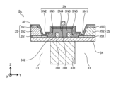
- Fig. 16 is an enlarged cross-sectional view showing a part of an actuator substrate 3c according to this embodiment, and corresponds to Fig. 8 of the first embodiment.
- the protective film 3P is illustrated in Fig. 16.
- the protective film 3P is positioned so as to cover the piezoelectric element 35 in the portion corresponding to the pressure chamber 31. Because the protective film 3P is positioned so as to cover the piezoelectric element 35, it is possible to reduce the possibility of moisture or ink adhering to the piezoelectric element 35. Furthermore, the protective film 3P is positioned so as to cover the common electrode 351 in the portion corresponding to the partition wall 331.
- the actuator substrate 3c according to this embodiment includes a first wiring 381 and a second wiring 382.
- the wiring 38 in the actuator substrate 3 according to the first embodiment is the first wiring 381 in the actuator substrate 3c according to this embodiment. Therefore, the first wiring 381 is located on the vibration plate 34 corresponding to the partition wall 331, similar to the wiring 38 in the first embodiment.
- the second wiring 382 is provided on the protective film 3P corresponding to the partition wall 331. The second wiring 382 is electrically connected to the first lead wiring 37, similar to the first wiring 381.
- the common electrode 351 according to this embodiment is set to ground potential, similar to the common electrode 351 in the first embodiment.
- the second wiring 382 is also provided on the protective film 3P corresponding to the partition 331, so compared to a case in which the first wiring 381 is provided only on the vibration plate 34 corresponding to the partition 331, the liquid ejection head 1 can be made smaller in the lateral direction while increasing the degree of freedom in routing the wiring 381, 382.
- the electric field generated from the first wiring 381 located on the diaphragm 34 corresponding to the partition 331 and the electric field generated from the second wiring 382 located on the protective film 3P corresponding to the partition 331 affect the second wiring 382 and the first wiring 381, respectively, which may result in electrical crosstalk.
- the liquid ejection head 1c is provided with a common electrode 351 set to ground potential between the first wiring 381 and the second wiring 382, so that the electric field between the first wiring 381 and the second wiring 382 in both directions can be shielded, reducing the possibility of electrical crosstalk occurring.
- FIG. 17 is an enlarged cross-sectional view showing a part of an actuator substrate 3d according to this embodiment, and corresponds to Fig. 8 of the first embodiment.
- the actuator substrate 3d according to this embodiment further includes a conductive member 3C.
- the conductive member 3C is located on the common electrode 351 corresponding to the partition wall 331.
- the liquid ejection head 1d according to this embodiment has a conductive member 3C on the common electrode 351, and the resistance value of the common electrode 351 can be reduced by conducting the common electrode 351 and the conductive member 3C. Because the resistance value of the common electrode 351 is reduced, the liquid ejection head 1d according to this embodiment can suppress distortion of the waveform of the voltage applied to the piezoelectric body 352. Because the distortion of the waveform can be suppressed, the liquid ejection head 1d according to this embodiment can reduce variation in the waveform applied to the piezoelectric body 352. Therefore, the liquid ejection head 1d according to this embodiment can reduce variation in liquid ejection.
- the thickness of the conductive member 3C may be made thicker than the thickness of the common electrode 351. By making the conductive member 3C thicker, the resistance value of the common electrode 351 is further reduced.
- the width of the conductive member 3C may be made wider than the width of the wiring 38. By making the width of the conductive member 3C wider, the resistance value of the common electrode 351 is further reduced. Examples of materials constituting the conductive member 3C include, but are not limited to, the same materials as those of the common electrode 351. For example, the conductive member 3C may be made of a metal with a low resistivity.
Landscapes
- Particle Formation And Scattering Control In Inkjet Printers (AREA)
Priority Applications (1)
| Application Number | Priority Date | Filing Date | Title |
|---|---|---|---|
| JP2024560125A JPWO2024111524A1 (https=) | 2022-11-24 | 2023-11-17 |
Applications Claiming Priority (2)
| Application Number | Priority Date | Filing Date | Title |
|---|---|---|---|
| JP2022-187506 | 2022-11-24 | ||
| JP2022187506 | 2022-11-24 |
Publications (1)
| Publication Number | Publication Date |
|---|---|
| WO2024111524A1 true WO2024111524A1 (ja) | 2024-05-30 |
Family
ID=91195680
Family Applications (1)
| Application Number | Title | Priority Date | Filing Date |
|---|---|---|---|
| PCT/JP2023/041525 Ceased WO2024111524A1 (ja) | 2022-11-24 | 2023-11-17 | 液体吐出ヘッドおよび記録装置 |
Country Status (2)
| Country | Link |
|---|---|
| JP (1) | JPWO2024111524A1 (https=) |
| WO (1) | WO2024111524A1 (https=) |
Citations (4)
| Publication number | Priority date | Publication date | Assignee | Title |
|---|---|---|---|---|
| US20120162320A1 (en) * | 2010-12-28 | 2012-06-28 | Seiko Epson Corporation | Piezoelectric element, liquid ejecting head, and liquid ejecting apparatus |
| JP2015006758A (ja) * | 2013-06-25 | 2015-01-15 | 株式会社リコー | 液滴吐出ヘッド及び液滴吐出装置 |
| JP2017094571A (ja) * | 2015-11-24 | 2017-06-01 | ブラザー工業株式会社 | 液体吐出装置 |
| JP2017132170A (ja) * | 2016-01-29 | 2017-08-03 | ブラザー工業株式会社 | 液体吐出装置、及び、液体吐出装置の製造方法 |
-
2023
- 2023-11-17 JP JP2024560125A patent/JPWO2024111524A1/ja active Pending
- 2023-11-17 WO PCT/JP2023/041525 patent/WO2024111524A1/ja not_active Ceased
Patent Citations (4)
| Publication number | Priority date | Publication date | Assignee | Title |
|---|---|---|---|---|
| US20120162320A1 (en) * | 2010-12-28 | 2012-06-28 | Seiko Epson Corporation | Piezoelectric element, liquid ejecting head, and liquid ejecting apparatus |
| JP2015006758A (ja) * | 2013-06-25 | 2015-01-15 | 株式会社リコー | 液滴吐出ヘッド及び液滴吐出装置 |
| JP2017094571A (ja) * | 2015-11-24 | 2017-06-01 | ブラザー工業株式会社 | 液体吐出装置 |
| JP2017132170A (ja) * | 2016-01-29 | 2017-08-03 | ブラザー工業株式会社 | 液体吐出装置、及び、液体吐出装置の製造方法 |
Also Published As
| Publication number | Publication date |
|---|---|
| JPWO2024111524A1 (https=) | 2024-05-30 |
Similar Documents
| Publication | Publication Date | Title |
|---|---|---|
| CN107020810B (zh) | 液体喷出装置及液体喷出装置的制造方法 | |
| EP1336491B1 (en) | Ink-jet head and ink-jet printer having the ink-jet head | |
| US20120069101A1 (en) | Inkjet head | |
| US10500856B2 (en) | Ink jet head and ink jet recording apparatus | |
| JP3951933B2 (ja) | インクジェットヘッド及びこれを有するインクジェットプリンタ | |
| JP5207546B2 (ja) | 液体吐出ヘッド、液体吐出ヘッドの製造方法及び画像形成装置 | |
| WO2019130408A1 (ja) | インクジェットヘッドの製造方法、インクジェット記録装置の製造方法、インクジェットヘッド及びインクジェット記録装置 | |
| US11760091B2 (en) | Liquid discharge head and recording apparatus | |
| JP7009857B2 (ja) | 液体噴射ヘッド、液体噴射装置、及び、圧電デバイス | |
| US8702210B2 (en) | Piezoelectric element, liquid ejecting head and liquid ejecting apparatus | |
| JP4138592B2 (ja) | インクジェットヘッドおよび印刷装置 | |
| WO2024111524A1 (ja) | 液体吐出ヘッドおよび記録装置 | |
| JP7328105B2 (ja) | 液体吐出ヘッドおよび記録装置 | |
| JP6547249B2 (ja) | 液体吐出装置の製造方法、及び、液体吐出装置 | |
| US11981134B2 (en) | Liquid discharge head and recording device | |
| JP7599481B2 (ja) | 液体吐出ヘッド及び記録装置 | |
| JP7646951B1 (ja) | 液体吐出ヘッド、ヘッドモジュール、および、記録装置 | |
| CN111204127B (zh) | 液体喷出头以及液体喷出装置 | |
| US12600122B2 (en) | Liquid discharge head and recording device | |
| EP4501645A1 (en) | Liquid discharge head and recording device | |
| US20250222693A1 (en) | Liquid discharge head and recording device | |
| JP2006248174A (ja) | 液体吐出ヘッド、その製造方法、及び、画像形成装置 | |
| US20250144935A1 (en) | Actuator, liquid discharge head, and production method of actuator | |
| JP7275769B2 (ja) | 圧電アクチュエータ及び液体吐出装置 | |
| US20250206021A1 (en) | Droplet discharge head and recording apparatus |
Legal Events
| Date | Code | Title | Description |
|---|---|---|---|
| 121 | Ep: the epo has been informed by wipo that ep was designated in this application |
Ref document number: 23894532 Country of ref document: EP Kind code of ref document: A1 |
|
| WWE | Wipo information: entry into national phase |
Ref document number: 2024560125 Country of ref document: JP |
|
| NENP | Non-entry into the national phase |
Ref country code: DE |
|
| 122 | Ep: pct application non-entry in european phase |
Ref document number: 23894532 Country of ref document: EP Kind code of ref document: A1 |