WO2024101359A1 - インクジェット用硬化性組成物、ledモジュール、及びledモジュールの製造方法 - Google Patents
インクジェット用硬化性組成物、ledモジュール、及びledモジュールの製造方法 Download PDFInfo
- Publication number
- WO2024101359A1 WO2024101359A1 PCT/JP2023/040071 JP2023040071W WO2024101359A1 WO 2024101359 A1 WO2024101359 A1 WO 2024101359A1 JP 2023040071 W JP2023040071 W JP 2023040071W WO 2024101359 A1 WO2024101359 A1 WO 2024101359A1
- Authority
- WO
- WIPO (PCT)
- Prior art keywords
- curable composition
- inkjet
- less
- led module
- weight
- Prior art date
- Legal status (The legal status is an assumption and is not a legal conclusion. Google has not performed a legal analysis and makes no representation as to the accuracy of the status listed.)
- Ceased
Links
Images


Classifications
-
- C—CHEMISTRY; METALLURGY
- C09—DYES; PAINTS; POLISHES; NATURAL RESINS; ADHESIVES; COMPOSITIONS NOT OTHERWISE PROVIDED FOR; APPLICATIONS OF MATERIALS NOT OTHERWISE PROVIDED FOR
- C09D—COATING COMPOSITIONS, e.g. PAINTS, VARNISHES OR LACQUERS; FILLING PASTES; CHEMICAL PAINT OR INK REMOVERS; INKS; CORRECTING FLUIDS; WOODSTAINS; PASTES OR SOLIDS FOR COLOURING OR PRINTING; USE OF MATERIALS THEREFOR
- C09D11/00—Inks
- C09D11/30—Inkjet printing inks
- C09D11/32—Inkjet printing inks characterised by colouring agents
- C09D11/324—Inkjet printing inks characterised by colouring agents containing carbon black
-
- C—CHEMISTRY; METALLURGY
- C09—DYES; PAINTS; POLISHES; NATURAL RESINS; ADHESIVES; COMPOSITIONS NOT OTHERWISE PROVIDED FOR; APPLICATIONS OF MATERIALS NOT OTHERWISE PROVIDED FOR
- C09D—COATING COMPOSITIONS, e.g. PAINTS, VARNISHES OR LACQUERS; FILLING PASTES; CHEMICAL PAINT OR INK REMOVERS; INKS; CORRECTING FLUIDS; WOODSTAINS; PASTES OR SOLIDS FOR COLOURING OR PRINTING; USE OF MATERIALS THEREFOR
- C09D201/00—Coating compositions based on unspecified macromolecular compounds
-
- C—CHEMISTRY; METALLURGY
- C09—DYES; PAINTS; POLISHES; NATURAL RESINS; ADHESIVES; COMPOSITIONS NOT OTHERWISE PROVIDED FOR; APPLICATIONS OF MATERIALS NOT OTHERWISE PROVIDED FOR
- C09D—COATING COMPOSITIONS, e.g. PAINTS, VARNISHES OR LACQUERS; FILLING PASTES; CHEMICAL PAINT OR INK REMOVERS; INKS; CORRECTING FLUIDS; WOODSTAINS; PASTES OR SOLIDS FOR COLOURING OR PRINTING; USE OF MATERIALS THEREFOR
- C09D4/00—Coating compositions, e.g. paints, varnishes or lacquers, based on organic non-macromolecular compounds having at least one polymerisable carbon-to-carbon unsaturated bond ; Coating compositions, based on monomers of macromolecular compounds of groups C09D183/00 - C09D183/16
-
- C—CHEMISTRY; METALLURGY
- C09—DYES; PAINTS; POLISHES; NATURAL RESINS; ADHESIVES; COMPOSITIONS NOT OTHERWISE PROVIDED FOR; APPLICATIONS OF MATERIALS NOT OTHERWISE PROVIDED FOR
- C09D—COATING COMPOSITIONS, e.g. PAINTS, VARNISHES OR LACQUERS; FILLING PASTES; CHEMICAL PAINT OR INK REMOVERS; INKS; CORRECTING FLUIDS; WOODSTAINS; PASTES OR SOLIDS FOR COLOURING OR PRINTING; USE OF MATERIALS THEREFOR
- C09D7/00—Features of coating compositions, not provided for in group C09D5/00; Processes for incorporating ingredients in coating compositions
- C09D7/40—Additives
- C09D7/41—Organic pigments; Organic dyes
-
- H—ELECTRICITY
- H10—SEMICONDUCTOR DEVICES; ELECTRIC SOLID-STATE DEVICES NOT OTHERWISE PROVIDED FOR
- H10H—INORGANIC LIGHT-EMITTING SEMICONDUCTOR DEVICES HAVING POTENTIAL BARRIERS
- H10H20/00—Individual inorganic light-emitting semiconductor devices having potential barriers, e.g. light-emitting diodes [LED]
- H10H20/80—Constructional details
- H10H20/85—Packages
Definitions
- the present invention relates to an inkjet curable composition that is applied by an inkjet method.
- the present invention also relates to an LED module that uses the inkjet curable composition, and a method for manufacturing an LED module.
- LED chips are used in a variety of electronic device applications.
- LED packages in which a lead frame and an LED chip are arranged on a substrate and the lead frame and LED chip are sealed with resin are widely used.
- a known example of such a large display device is one in which a number of the above-mentioned LED packages are arranged to create small LED modules, and then the LED modules are connected together.
- LEDs can be lit up in white, red, blue, green, etc. to display something.
- Patent Document 1 discloses a self-luminous display comprising a light-emitting module in which multiple light-emitting elements are mounted on a wiring board, a black encapsulant sheet that contains an olefin resin and has a visible light transmittance of 5% to 70%, and a transparent optical layer.
- the black encapsulant sheet is laminated to the light-emitting module, covering the light-emitting elements and the surface of the wiring board.
- the inventors attempted to form partition walls and surface layers by incorporating a colorant such as carbon black into the curable composition to suppress discoloration when the LED module is viewed from an angle.
- a colorant such as carbon black
- the inventors found that when carbon black is added to a conventional curable composition, the ejection properties using an inkjet device tend to deteriorate.
- This specification discloses the following inkjet curable composition, LED module, and method for manufacturing an LED module.
- a curable composition for inkjet comprising a photocurable compound having two or more photopolymerizable functional groups and no cyclic ether group, a thermosetting compound having a cyclic ether group, a photopolymerization initiator, a thermosetting agent, a colorant, and a dispersant, wherein the colorant comprises carbon black, the carbon black has an average particle size of 40 nm or more and 100 nm or less, and when a cured product of the curable composition for inkjet having a thickness of 30 ⁇ m is irradiated with light, the b* value of the reflected light of the cured product in the L*a*b* color system is -3 or more and 3 or less.
- Item 2 The curable composition for inkjet according to item 1, wherein the acid value of the dispersant is 10 mgKOH/g or more and 150 mgKOH/g or less, and the amine value of the dispersant is 10 mgKOH/g or more and 100 mgKOH/g or less.
- Item 4 The curable composition for inkjet according to any one of items 1 to 3, wherein the content of the carbon black is 0.1% by weight or more and 5.0% by weight or less in 100% by weight of the curable composition for inkjet.
- Item 5 The curable composition for inkjet according to any one of items 1 to 4, wherein the colorant further comprises a colorant other than carbon black.
- Item 6 The curable composition for inkjet according to any one of items 1 to 5, wherein the colorant further contains a phthalocyanine compound.
- Item 7 The curable composition for inkjet according to any one of items 1 to 6, wherein the photocurable compound has two or more (meth)acryloyl groups and includes a photocurable compound having a dicyclopentadiene skeleton.
- thermosetting compound includes 4-hydroxybutyl (meth)acrylate glycidyl ether.
- Item 9 The inkjet curable composition according to any one of items 1 to 8, which is used to form a partition wall in an LED module.
- Item 10 An LED module comprising a substrate, an LED chip disposed on a first surface of the substrate, and a partition wall disposed on the first surface of the substrate, the partition wall being disposed on the first surface of the substrate so as to surround the LED chip, and the partition wall being a cured product of the inkjet curable composition described in any one of items 1 to 9.
- a method for manufacturing an LED module comprising: a coating step of coating a first surface of a substrate with the inkjet curable composition according to any one of items 1 to 9 by an inkjet method to form a composition layer; a photocuring step of irradiating the coated inkjet curable composition with light to cure the inkjet curable composition and form a B-stage product; a thermal curing step of thermally curing the B-stage product by heating to form a partition wall; and a step of arranging an LED chip on the first surface of the substrate and inside an area surrounded by the partition wall.
- the inkjet curable composition according to the present invention is an inkjet curable composition that includes a photocurable compound having two or more photopolymerizable functional groups and no cyclic ether group, a thermosetting compound having a cyclic ether group, a photopolymerization initiator, a thermosetting agent, a colorant, and a dispersant.
- the colorant includes carbon black, and the average particle size of the carbon black is 40 nm or more and 100 nm or less.
- the inkjet curable composition according to the present invention when a cured product of the inkjet curable composition having a thickness of 30 ⁇ m is irradiated with light, the b* value of the reflected light of the cured product in the L*a*b* color system is -3 or more and 3 or less. Since the inkjet curable composition according to the present invention has the above configuration, it is possible to improve the inkjet ejection property and further to suppress discoloration when the obtained LED module is viewed obliquely.
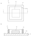
- FIG. 1( a ) is a plan view that typically illustrates an LED module obtained using the curable composition for inkjet according to the first embodiment of the present invention
- FIG. 1( b ) is a cross-sectional view that typically illustrates the LED module
- FIG. 2 is a cross-sectional view that illustrates an LED module obtained using the curable composition for inkjet according to the second embodiment of the present invention
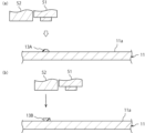
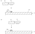
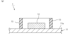
- FIG. 6G is a cross-sectional view for explaining each step of the method for manufacturing the LED module shown in FIG.
- curable composition for inkjet printing The curable composition for inkjet according to the present invention (hereinafter, may be referred to as “curable composition”) is used for inkjet coating.
- the curable composition according to the present invention contains the following components:
- a photocurable compound having two or more photopolymerizable functional groups and no cyclic ether group (hereinafter, sometimes referred to as “photocurable compound (A)")
- Thermosetting compound having a cyclic ether group (hereinafter, may be referred to as “thermosetting compound (B)”)
- Photopolymerization initiator C
- Heat curing agent D
- Colorant E
- Dispersant F
- the curable composition has photocurable and thermosetting properties.
- the curable composition is preferably cured by irradiation with light and heating before use. It is more preferable that the curable composition is cured by heating after curing is promoted by irradiation with light.
- the curable composition can be applied by an inkjet method.
- an inkjet device When applying the curable composition by an inkjet method, an inkjet device is used.
- the inkjet device has an inkjet head.
- the inkjet head has an inkjet nozzle.
- the curable composition is different from a composition applied by screen printing, a composition applied by a dispenser, and the like.
- the curable composition is preferably used for, for example, light-emitting diodes (LEDs) (use of the curable composition for light-emitting diodes (LEDs)).
- the curable composition is preferably a curable composition for inkjet and LEDs.
- the curable composition is particularly preferably used for forming a partition in an LED module (use of the curable composition for forming a partition in an LED module).
- the curable composition is preferably a curable composition for forming a partition.
- the curable composition is preferably used for forming a partition in the gap between a plurality of LED chips (use of the curable composition for forming a partition in the gap between a plurality of LED chips).
- the curable composition is preferably used for forming a partition on the periphery of the mounting area of the LED chip (use of the curable composition for forming a partition on the periphery of the mounting area of the LED chip).
- This can increase the efficiency of use of light generated from the LED chip, and can suppress discoloration when the LED module is viewed obliquely.
- the LED chip is an LED chip that emits ultraviolet light (UV-LED chip)
- the luminous efficiency of the LED chip itself may be low.
- the use of the curable composition can increase the light extraction efficiency, so the curable composition can be particularly suitably used when the LED chip is an LED chip that emits ultraviolet light.
- the curable composition is also preferably used to form a surface layer in an LED module.
- the curable composition is preferably a curable composition for forming a surface layer.
- the curable composition is preferably used to form a surface layer disposed above a plurality of LED chips.
- the surface layer may be disposed above a plurality of LED chips, may be disposed above gaps between the plurality of LED chips, or may be disposed both above the plurality of LED chips and above the gaps.
- the surface layer may be disposed above a light-transmitting layer disposed above the plurality of LED chips. This makes it possible to suppress discoloration when the LED module is viewed obliquely.
- the above-mentioned curable composition is particularly suitable for use in LED modules using the COB method or the COG method. It is more preferable that the above-mentioned curable composition is used as a curable composition for forming a partition wall or a curable composition for forming a surface layer in an LED module using the COB method or the COG method. The above-mentioned curable composition is also suitable for use as a curable composition for forming a black matrix of an LED module or a bezel of an LED module.
- the curable composition may be used for purposes other than LEDs.
- the curable composition may be suitably used as a marking material for electronic components, a curable composition for forming a light shielding material for an infrared sensor, and a curable composition for forming a light shielding material for a camera module.
- the b* value of the reflected light from the cured product in the L*a*b* color system is -3 or more and 3 or less. If the b* value is less than -3, the LED module with the LED turned on will have a bluish color when viewed obliquely, and discoloration cannot be sufficiently suppressed. If the b* value is more than 3, the LED module with the LED turned on will have a reddish color when viewed obliquely, and discoloration cannot be sufficiently suppressed.
- the b* value can be measured, for example, by the following method.
- ultraviolet light UV-LED
- an integrated light quantity of 1000 mJ/cm 2 so that the illuminance at a wavelength of 365 nm is 1000 mW/cm 2 to prepare a B-stage product of the curable composition.
- the obtained B-stage product is heated at 160° C. for 1 hour to form a cured product of the curable composition having a thickness of 30 ⁇ m.
- L* value, a* value, and b* value in the L*a*b* color system are preferably measured using a spectrophotometer (for example, "CM-26dG” manufactured by Konica Minolta) in accordance with JIS Z8781-4:2013.
- a spectrophotometer for example, "CM-26dG” manufactured by Konica Minolta
- the present inventors focused on the influence of short-wavelength scattered light and the color of the cured product of the curable composition on discoloration when the LED module is viewed obliquely.
- the present inventors found that yellowing of the cured product of the curable composition (particularly, the cured product of a thermosetting compound or the cured product of a photocurable compound) significantly affects discoloration when the LED module is viewed obliquely.
- the present inventors found that when the cured product of the curable composition (particularly, the cured product of a thermosetting compound or the cured product of a photocurable compound) yellows, the b* value of the reflected light of the cured product in the L*a*b* color system tends to be large.
- the b* value is controlled within a specific range, so that the influence of short-wavelength scattered light and the color of the cured product of the curable composition can be suppressed, and discoloration when the LED module is viewed obliquely can be suppressed.
- the light irradiated to the cured product is not particularly limited.
- the light may be ultraviolet light, electron beam, alpha ray, beta ray, gamma ray, X-ray, neutron beam, etc.
- the light may be white light, blue light, red light, or green light.
- the wavelength of the light is preferably 250 nm or more, more preferably 300 nm or more, and is preferably 850 nm or less, more preferably 800 nm or less.
- the b* value is preferably -2.5 or more, more preferably -2 or more, even more preferably -1 or more, and is preferably 2.5 or less, more preferably 2 or less, even more preferably 1 or less. If the b* value is equal to or more than the lower limit and equal to or less than the upper limit, discoloration of the resulting LED module when viewed obliquely can be further effectively suppressed.
- the a* value is preferably -5 or more, more preferably -4 or more, even more preferably -3 or more, and is preferably 4 or less, more preferably 3 or less, even more preferably 2 or less. If the a* value is equal to or greater than the lower limit and equal to or less than the upper limit, discoloration of the resulting LED module when viewed obliquely can be more effectively suppressed.
- the L* value is preferably 1 or more, more preferably 3 or more, even more preferably 10 or more, particularly preferably 20 or more, and most preferably 30 or more, and is preferably 90 or less, more preferably 80 or less, and even more preferably 70 or less.
- L* value is equal to or greater than the lower limit and equal to or less than the upper limit, discoloration of the resulting LED module when viewed obliquely can be further effectively suppressed.
- the color difference ⁇ E*ab calculated from the L*, a*, and b* values is preferably 10 or less, more preferably 9 or less, even more preferably 8 or less, particularly preferably 7 or less, and most preferably 0.
- the color difference ⁇ E*ab is equal to or less than the upper limit, the light can be dispersed even better, and discoloration of the resulting LED module when viewed obliquely can be suppressed even more effectively.
- the color difference ⁇ E*ab may be 0 or more, 0.5 or more, or 1.0 or more.
- Methods for adjusting the b* value to a preferred range include using carbon black with a specific average particle size, as described below, using two or more types of carbon black with different average particle sizes in combination, adjusting the amount of carbon black, selecting a thermosetting compound and a photocurable compound that are less likely to yellow, adding an antioxidant, and further adding a colorant.
- the b* value can be increased by using carbon black with a small average particle size, and the b* value can be decreased by using carbon black with a large average particle size.
- the curable composition is preferably in a liquid state at 25°C.
- a liquid state also includes a paste state.
- the viscosity ( ⁇ 25) of the curable composition at 25°C is preferably 40 mPa ⁇ s or more, more preferably 60 mPa ⁇ s or more, even more preferably 80 mPa ⁇ s or more, and is preferably 500 mPa ⁇ s or less, more preferably 400 mPa ⁇ s or less, even more preferably 300 mPa ⁇ s or less.
- the viscosity ( ⁇ 25) is equal to or more than the lower limit and equal to or less than the upper limit, the inkjet ejection properties can be further improved.
- the above viscosity ( ⁇ 25) is preferably measured using an E-type viscometer (e.g., "TVE22L” manufactured by Toki Sangyo Co., Ltd.) at 25°C and 10 rpm for the curable composition immediately after preparation.
- E-type viscometer e.g., "TVE22L” manufactured by Toki Sangyo Co., Ltd.
- the curable composition When ejected by the inkjet device, the curable composition is preferably ejected in a heated state of 40°C or more and 100°C or less. From the viewpoint of increasing the height accuracy of the partition walls and the thickness accuracy of the surface layer, and making it difficult for voids to occur in the partition walls and the surface layer, it is preferable to apply the curable composition while circulating it.
- the inkjet device preferably has an ink tank in which the curable composition is stored, a discharge part connected to the ink tank and from which the curable composition is discharged, and a circulation flow path part having one end connected to the discharge part and the other end connected to the ink tank and through which the curable composition flows.
- the curable composition that was not ejected from the ejection section is preferably applied while circulating the curable composition by flowing it through the circulation flow path section and moving it to the ink tank.
- the curable composition is applied while circulating, the height accuracy of the partition walls and the thickness accuracy of the surface layer can be improved, and voids can be made less likely to occur in the partition walls and the surface layer.
- the glass transition temperature (Tg) of the cured product of the curable composition is preferably 80°C or higher, more preferably 90°C or higher, and even more preferably 100°C or higher, and is preferably 190°C or lower, more preferably 180°C or lower, and even more preferably 170°C or lower.
- Tg glass transition temperature
- the glass transition temperature (Tg) of the cured product of the curable composition can be measured using a dynamic viscoelasticity measuring device at a temperature rise rate of 10°C/min and a measurement frequency of 10 Hz.
- the dynamic viscoelasticity measuring device include the "DVA-200" manufactured by IT Measurement and Control Co., Ltd.
- a cured product of the curable composition can be obtained, for example, by the following method.
- the curable composition is applied onto the surface of a glass substrate using an inkjet device, and then irradiated with ultraviolet light (UV-LED) with an integrated light quantity of 1000 mJ/ cm2 so that the illuminance at a wavelength of 365 nm is 1000 mW/ cm2 , to produce a B-stage product of the curable composition.
- UV-LED ultraviolet light
- the obtained B-stage product is heated at 160°C for 1 hour to form a cured product of the curable composition.
- (meth)acryloyl means either or both of “acryloyl” and “methacryloyl”
- (meth)acrylate means either or both of "acrylate” and “methacrylate”.
- the curable composition contains a photocurable compound (A) having two or more photopolymerizable functional groups and not having a cyclic ether group.
- the curable composition contains the photocurable compound (A), which further improves the inkjet ejection properties and allows the curable composition to be positioned accurately.
- the photopolymerizable functional group may be, for example, a (meth)acryloyl group or a vinyl group. From the viewpoint of efficiently proceeding with the photocuring reaction, it is preferable that the photopolymerizable functional group is at least one type of photopolymerizable functional group selected from the group consisting of a (meth)acryloyl group and a vinyl group.
- the photocurable compound (A) may have two or more (meth)acryloyl groups, may have two or more vinyl groups, or may have both a (meth)acryloyl group and a vinyl group.
- the photocurable compound (A) may not have a (meth)acryloyl group, and may not have a vinyl group.
- the photocurable compound (A) may be a photocurable compound (A) having two or more (meth)acryloyl groups and no cyclic ether group, or may be a photocurable compound (A) having two or more vinyl groups and no cyclic ether group.
- the photocurable compound (A) may be a photocurable compound (A) having both a (meth)acryloyl group and a vinyl group, and no cyclic ether group.
- the photocurable compound (A) having two or more (meth)acryloyl groups and no cyclic ether group may be a bifunctional (meth)acrylate compound, a bifunctional or higher (meth)acrylate compound, a trifunctional (meth)acrylate compound, or a trifunctional or higher (meth)acrylate compound.
- the photocurable compound (A) may be a (meth)acrylate compound having 20 or less functionalities, a (meth)acrylate compound having 10 or less functionalities, or a (meth)acrylate compound having 5 or less functionalities.
- the functionality corresponds to the number of (meth)acryloyl groups. Only one type of the photocurable compound (A) may be used, or two or more types may be used in combination.
- the photocurable compound (A) having two or more (meth)acryloyl groups and no cyclic ether group may have two (meth)acryloyl groups, two or more, three, three or more, 20 or less, 10 or less, or 5 or less.
- the photocurable compound (A) contains a photocurable compound having an alicyclic skeleton.
- bifunctional (meth)acrylate compounds having an alicyclic skeleton examples include ethoxylated cyclohexanemethanol di(meth)acrylate, tricyclodecane dimethanol di(meth)acrylate, 1,3-adamantanediol di(meth)acrylate, and propoxylated cyclohexanemethanol di(meth)acrylate.
- trifunctional (meth)acrylate compounds having an alicyclic skeleton examples include pentaerythritol triacrylate-isophorone diisocyanate-urethane prepolymer.
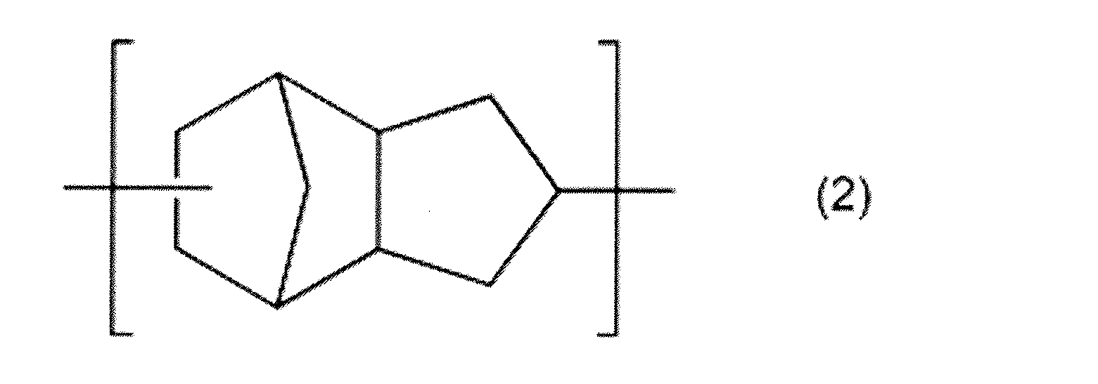
- the alicyclic skeleton is a dicyclopentadiene skeleton.
- the photocurable compound (A) contains a (meth)acrylate compound represented by the following formula (1).
- R1 and R2 each represent a hydrogen atom or a methyl group
- R3 represents an alkylene group
- R1 and R2 may be the same or different.
- the number of carbon atoms in the alkylene group of R3 in the above formula (1) is preferably 2 or more, more preferably 4 or more, even more preferably 6 or more, and preferably 14 or less, more preferably 12 or less, even more preferably 9 or less.
- R3 in the above formula (1) is an alkylene group having a carbon number of 6 to 9.
- Examples of the (meth)acrylate compound represented by the above formula (1) include decanediol di(meth)acrylate, nonanediol di(meth)acrylate, and hexanediol di(meth)acrylate.
- Examples of the photocurable compound (A) having two or more vinyl groups include vinyl ethers, ethylene derivatives, and styrene derivatives.
- the photocurable compound (A) contains a photocurable compound having two or more (meth)acryloyl groups and a dicyclopentadiene skeleton. That is, it is preferable that the photocurable compound (A) contains a photocurable compound having two or more (meth)acryloyl groups, a dicyclopentadiene skeleton, and no cyclic ether group.
- the photocurable compound (A) contains a (meth)acrylate compound having two (meth)acryloyl groups and a dicyclopentadiene skeleton.
- the double bond portion of dicyclopentadiene may be reacted.
- the dicyclopentadiene skeleton in the photocurable compound (A) may be a skeleton represented by the following formula (2). In the following formula (2), the right and left ends are bonding sites with other groups.
- the photocurable compound (A) preferably contains ethoxylated cyclohexanemethanol di(meth)acrylate or tricyclodecane dimethanol di(meth)acrylate, and more preferably contains tricyclodecane dimethanol di(meth)acrylate.
- Tricyclodecane dimethanol di(meth)acrylate has a skeleton represented by the above formula (2).
- the glass transition temperature (Tg) of the homopolymer of the photocurable compound (A) is preferably 100°C or higher, more preferably 150°C or higher, even more preferably 190°C or higher, and is preferably 250°C or lower, more preferably 220°C or lower.
- Tg glass transition temperature
- the glass transition temperature (Tg) of the homopolymer of the photocurable compound (A) refers to the glass transition temperature of a homopolymer having a degree of polymerization of 3000 to 4000 (preferably 3500).
- the glass transition temperature can be measured in accordance with JIS K7121 using a dynamic viscoelasticity measuring device at a temperature rise rate of 10°C/min and a measuring frequency of 10 Hz.
- Examples of the dynamic viscoelasticity measuring device include the "DVA-200" manufactured by IT Measurement and Control Co., Ltd.
- the content of the photocurable compound (A) in 100% by weight of the curable composition is preferably 10% by weight or more, more preferably 20% by weight or more, even more preferably 30% by weight or more, and is preferably 80% by weight or less, more preferably 70% by weight or less, even more preferably 60% by weight or less.
- the content of the photocurable compound (A) is equal to or more than the lower limit and equal to or less than the upper limit, the inkjet ejection properties can be further improved and the curable composition can be accurately positioned.
- the curable composition contains a thermosetting compound (B) having a cyclic ether group.
- the curable composition contains the thermosetting compound (B), which can improve adhesion between the partition wall and the surface layer and the inkjet target area.
- the cyclic ether group may be an epoxy group, an oxetanyl group, or the like.
- the epoxy group may be a glycidyl group.
- the thermosetting compound (B) is a thermosetting compound having an epoxy group (epoxy compound). Only one type of the thermosetting compound (B) may be used, or two or more types may be used in combination.
- the above epoxy compounds include bisphenol A type epoxy compounds, bisphenol F type epoxy compounds, bisphenol S type epoxy compounds, phenol novolac type epoxy compounds, biphenyl type epoxy compounds, biphenyl novolac type epoxy compounds, biphenol type epoxy compounds, naphthalene type epoxy compounds, fluorene type epoxy compounds, phenol aralkyl type epoxy compounds, naphthol aralkyl type epoxy compounds, dicyclopentadiene type epoxy compounds, anthracene type epoxy compounds, epoxy compounds having an adamantane skeleton, epoxy compounds having a tricyclodecane skeleton, naphthylene ether type epoxy compounds, and epoxy compounds having a triazine nucleus in the skeleton.
- the thermosetting compound (B) may be a photo- and thermosetting compound.
- the thermosetting compound (B) may have a cyclic ether group and a (meth)acryloyl group, or may have an epoxy group and a (meth)acryloyl group.
- the thermosetting compound (B) is a curable compound different from the first (meth)acrylate compound and the second (meth)acrylate compound.
- thermosetting compound having the above-mentioned epoxy group and (meth)acryloyl group examples include glycidyl (meth)acrylate, allyl glycidyl ether, 4-hydroxybutyl (meth)acrylate glycidyl ether, and 3,4-epoxycyclohexylmethyl (meth)acrylate.
- thermosetting compound (B) preferably contains glycidyl (meth)acrylate or 4-hydroxybutyl (meth)acrylate glycidyl ether, and more preferably contains 4-hydroxybutyl (meth)acrylate glycidyl ether.
- the content of the thermosetting compound (B) is preferably 4% by weight or more, more preferably 5% by weight or more, even more preferably 6% by weight or more, preferably 20% by weight or less, more preferably 18% by weight or less, and even more preferably 16% by weight or less.
- the content of the thermosetting compound (B) is equal to or more than the lower limit and equal to or less than the upper limit, the adhesion between the partition wall and the surface layer and the inkjet target part is improved, and discoloration of the obtained LED module when viewed obliquely can be more effectively suppressed.
- the curable composition contains a photopolymerization initiator (C).
- the curable composition contains the photopolymerization initiator (C), so the curable composition can be cured by irradiation with light.
- the photopolymerization initiator (C) may be a photoradical polymerization initiator, a photocationic polymerization initiator, or the like.
- the photopolymerization initiator (C) is preferably a photoradical polymerization initiator. Only one type of the photopolymerization initiator (C) may be used, or two or more types may be used in combination.
- the photoradical polymerization initiator is a compound that generates radicals by irradiation with light and initiates a radical polymerization reaction.
- the photoradical polymerization initiator include benzoin compounds such as benzoin, benzoin methyl ether, benzoin ethyl ether, and benzoin isopropyl ether; alkylphenone compounds such as 1-hydroxycyclohexyl phenyl ketone, 2-hydroxy-2-methylpropiophenone, and ⁇ -hydroxyalkylphenone; acetophenone compounds such as acetophenone, aminoacetophenone, 2,2-dimethoxy-2-phenylacetophenone, 2,2-diethoxy-2-phenylacetophenone, and 1,1-dichloroacetophenone; 2-methyl-1-[4-(methylthio)phenyl]-2- Aminoacetophenone compounds such as morpholinopropan-1-one, 2-benzyl-2-dimethylamino-1-(4-morph
- the photopolymerization initiator (C) contains an aminoacetophenone compound.
- a photopolymerization initiator assistant may be used together with the above-mentioned photoradical polymerization initiator.
- the photopolymerization initiator assistant include N,N-dimethylaminobenzoic acid ethyl ester, N,N-dimethylaminobenzoic acid isoamyl ester, pentyl-4-dimethylaminobenzoate, triethylamine, and triethanolamine.
- the above-mentioned photopolymerization initiator assistant may be used alone or in combination of two or more kinds.
- Titanocene compounds such as CGI-784 (manufactured by Ciba Specialty Chemicals), which have absorption in the visible light region, may also be used to promote the photoreaction.
- the above cationic photopolymerization initiators include sulfonium salts, iodonium salts, metallocene compounds, and benzoin tosylate.
- the above cationic photopolymerization initiators may be used alone or in combination of two or more.
- the content of the photopolymerization initiator (C) in 100% by weight of the curable composition is preferably 4% by weight or more, more preferably 5% by weight or more, and preferably 15% by weight or less, more preferably 12% by weight or less.
- the curability of the curable composition can be increased, and discoloration of the resulting LED module when viewed obliquely can be more effectively suppressed.
- the content of the photopolymerization initiator (C) is preferably 4 parts by weight or more, more preferably 5 parts by weight or more, and preferably 20 parts by weight or less, more preferably 15 parts by weight or less, relative to 100 parts by weight of the photocurable compound (A).
- the content of the photopolymerization initiator (C) is equal to or more than the lower limit and equal to or less than the upper limit, the curability of the curable composition can be increased, and discoloration of the resulting LED module when viewed obliquely can be more effectively suppressed.
- the curable composition contains a heat curing agent (D).
- thermosetting agent (D) which can enhance the curability of the above curable composition (thermosetting compound (B)).
- the above-mentioned heat curing agent (D) includes organic acids, amine compounds, amide compounds, hydrazide compounds, imidazole compounds, imidazoline compounds, phenol compounds, urea compounds, polysulfide compounds, and acid anhydrides.
- the above-mentioned heat curing agent (D) may be used alone or in combination of two or more kinds.
- the above amine compounds include aliphatic polyamines, alicyclic polyamines, aromatic polyamines, hydrazides, and guanidine derivatives.
- the above amine compounds may be modified polyamine compounds such as amine-epoxy adducts.
- the above amine compounds may be adducts of the above amine compounds.
- Examples of the adducts of the above amine compounds include epoxy compound-added polyamines (reactants of epoxy compounds and polyamines), Michael addition polyamines (reactants of ⁇ , ⁇ -unsaturated ketones and polyamines), Mannich addition polyamines (condensates of polyamines with formalin and phenols), thiourea-added polyamines (reactants of thiourea and polyamines), and ketone-blocked polyamines (reactants of ketone compounds and polyamines (ketimines)).
- the above-mentioned aliphatic polyamines include diethylenetriamine, triethylenetetramine, tetraethylenepentamine, and diethylaminopropylamine.
- the above alicyclic polyamines include menthene diamine, isophorone diamine, N-aminoethylpiperazine, 3,9-bis(3-aminopropyl)-2,4,8,10-tetraoxaspiro(5,5)undecane adduct, bis(4-amino-3-methylcyclohexyl)methane, and bis(4-aminocyclohexyl)methane.
- the aromatic polyamines include m-phenylenediamine, p-phenylenediamine, o-xylylenediamine, m-xylylenediamine, p-xylylenediamine, 4,4-diaminodiphenylmethane, 4,4'-diamino-3,3'-diethyl-5,5'-dimethyldiphenylmethane, 4,4-diaminodiphenylpropane, 4,4-diaminodiphenylsulfone, 4,4-diaminodicyclohexane, bis(4-aminophenyl)phenylmethane, 1,5-diaminonaphthalene, 1,1-bis(4-aminophenyl)cyclohexane, 2,2-bis[(4-aminophenoxy)phenyl]propane, bis[4-(3-aminophenoxy)phenyl]sulfone, 1,3
- hydrazides examples include carbodihydrazide, adipic acid dihydrazide, sebacic acid dihydrazide, dodecanedioic acid dihydrazide, and isophthalic acid dihydrazide.
- guanidine derivatives include dicyandiamide, 1-o-tolyldiguanide, ⁇ -2,5-dimethylguanide, ⁇ , ⁇ -diphenyldiguanide, ⁇ , ⁇ -bisguanylguanidinodiphenyl ether, p-chlorophenyldiguanide, ⁇ , ⁇ -hexamethylenebis[ ⁇ -(p-chlorophenol)]diguanide, phenyldiguanide oxalate, acetylguanidine, and diethylcyanoacetylguanidine.
- the above-mentioned phenolic compounds include polyhydric phenolic compounds.
- Examples of the above-mentioned polyhydric phenolic compounds include phenol, cresol, ethylphenol, butylphenol, octylphenol, bisphenol A, tetrabromobisphenol A, bisphenol F, bisphenol S, 4,4'-biphenylphenol, phenol novolac resins containing a naphthalene skeleton, phenol novolac resins containing a xylylene skeleton, phenol novolac resins containing a dicyclopentadiene skeleton, and phenol novolac resins containing a fluorene skeleton.
- acid anhydrides examples include phthalic anhydride, tetrahydrophthalic anhydride, hexahydrophthalic anhydride, methyltetrahydrophthalic anhydride, methylnadic anhydride, dodecylsuccinic anhydride, chlorendic anhydride, pyromellitic anhydride, benzophenonetetracarboxylic anhydride, methylcyclohexenetetracarboxylic anhydride, trimellitic anhydride, and polyazelaic anhydride.
- the content of the heat curing agent (D) in 100% by weight of the curable composition is preferably 1% by weight or more, more preferably 2% by weight or more, and preferably 10% by weight or less, more preferably 8% by weight or less.
- the content of the heat curing agent (D) is equal to or more than the lower limit and equal to or less than the upper limit, the curability of the curable composition can be increased, and discoloration of the resulting LED module when viewed obliquely can be more effectively suppressed.
- the content of the heat curing agent (D) relative to 100 parts by weight of the thermosetting compound (B) is preferably 10 parts by weight or more, more preferably 20 parts by weight or more, even more preferably 25 parts by weight or more, particularly preferably 30 parts by weight or more, and is preferably 60 parts by weight or less, more preferably 55 parts by weight or less, and even more preferably 50 parts by weight or less.
- the content of the heat curing agent (D) is equal to or more than the lower limit and equal to or less than the upper limit, the curability of the curable composition can be increased, and discoloration can be more effectively suppressed when the obtained LED module is viewed obliquely.
- the curable composition includes a colorant (E).
- the colorant (E) contains carbon black. Since the colorant (E) contains carbon black, it can conceal the wiring arranged between the LED chips (improve wiring concealment), and can suppress discoloration when the resulting LED module is viewed obliquely.
- the carbon black is a black inorganic pigment.
- the carbon black has an average particle diameter of 40 nm or more and 100 nm or less.
- the carbon black has an average particle diameter of 40 nm or more, it is easy to scatter transmitted light of long wavelengths, and the b* value can be easily adjusted to a smaller value (e.g., 3 or less), and discoloration when the LED module is viewed obliquely can be suppressed.
- the carbon black has an average particle diameter of 100 nm or less, it is easy to scatter transmitted light of short wavelengths, and the b* value can be easily adjusted to a larger value (e.g., -3 or more), and discoloration when the LED module is viewed obliquely can be suppressed.
- the carbon black since the carbon black has an average particle diameter of 40 nm or more and 100 nm or less, it is possible to improve inkjet ejection properties.
- the average particle size of the carbon black is preferably 45 nm or more, more preferably 50 nm or more, and even more preferably 60 nm or more, and is preferably 95 nm or less, more preferably 90 nm or less, and even more preferably 80 nm or less.
- the average particle size of the carbon black is preferably the average primary particle size.
- the average particle size of the carbon black is preferably measured using an electron microscope to determine the arithmetic mean particle size (D50) of the carbon black.
- the carbon black may be of one type only, or may be of two or more types with different average particle sizes.
- the curable composition (colorant (E)) contains two or more types of carbon black with different average particle sizes, it is preferable that the average particle size of all the carbon black in the curable composition is 40 nm or more and 100 nm or less.
- the colorant (E) may or may not further contain a colorant other than carbon black. From the viewpoint of further enhancing the wiring concealment and further suppressing discoloration when the LED module is viewed from an angle, it is preferable that the colorant (E) further contains a colorant other than carbon black. Note that, from the viewpoint of easily adjusting the b* value to a preferred range, when the content of the carbon black exceeds 2.0 wt % in 100 wt % of the curable composition, it is preferable that the colorant (E) does not contain a colorant other than carbon black.
- colorants other than carbon black examples include dyes and pigments.
- the colorants other than carbon black may be used alone or in combination of two or more.
- the above dyes include pyrazole azo dyes, anilino azo dyes, triphenylmethane dyes, anthraquinone dyes, anthrapyridone dyes, benzylidene dyes, oxol dyes, pyrazolotriazole azo dyes, pyridone azo dyes, cyanine dyes, phenothiazine dyes, pyrrolopyrazole azomethine dyes, xathene dyes, phthalocyanine dyes, benzopyran dyes, indigo dyes, pyrromethene dyes, triarylmethane dyes, azomethine dyes, perylene dyes, perinone dyes, quataryl dyes, and quinophthalone dyes.
- the above dyes may be acid dyes, direct dyes, basic dyes, mordant dyes, acid mordant dyes, azoic dyes, disperse dyes, oil-soluble dyes, food dyes, and dyes that are blackened by mixing two or more of these derivatives.
- the above dyes may be used alone or in combination of two or more.
- the pigment may be an organic pigment or an inorganic pigment.
- the organic pigment may be an organic pigment having a metal atom or an organic pigment not having a metal atom. Only one type of the pigment may be used, or two or more types may be used in combination.
- the organic pigments include phthalocyanine compounds, quinacridone compounds, azo compounds, pentaphene compounds, perylene compounds, indole compounds, and dioxazine compounds.
- the above phthalocyanine compounds include copper phthalocyanine compounds, etc.
- the above inorganic pigments include carbon nanotubes, graphene, iron oxide, zinc oxide, titanium oxide, calcium carbonate, alumina, kaolin clay, calcium silicate, magnesium oxide, magnesium hydroxide, aluminum hydroxide, magnesium carbonate, talc, feldspar powder, mica, barite, barium carbonate, silica, and glass beads.
- the colorant other than the carbon black contains a blue dye. From the viewpoint of better suppressing discoloration when the LED module is viewed obliquely, it is preferable that the colorant other than the carbon black contains an anthraquinone dye or a phthalocyanine compound, and it is more preferable that it contains a phthalocyanine compound. From the viewpoint of better suppressing discoloration when the LED module is viewed obliquely, it is preferable that the colorant further contains an anthraquinone dye or a phthalocyanine compound, and it is more preferable that it further contains a phthalocyanine compound.
- the content of the colorant (E) in 100% by weight of the curable composition is preferably 0.1% by weight or more, more preferably 0.5% by weight or more, and is preferably 5.0% by weight or less, more preferably 4.0% by weight or less, even more preferably 2.0% by weight or less, and particularly preferably 1.5% by weight or less.
- the content of the colorant (E) is equal to or more than the lower limit and equal to or less than the upper limit, the wiring concealment can be further improved, and discoloration when the LED module is viewed from an angle can be further suppressed.
- the content of the carbon black is preferably 0.1% by weight or more, more preferably 0.5% by weight or more, and is preferably 5.0% by weight or less, more preferably 4.0% by weight or less, even more preferably 3.0% by weight or less, particularly preferably 2.0% by weight or less, and most preferably 1.5% by weight or less.
- the content of the carbon black is equal to or more than the lower limit and equal to or less than the upper limit, the wiring concealment can be further improved and the curability can be improved.
- the colorant (E) contains two or more types of carbon black having different average particle sizes, the content of the carbon black is the total content of the carbon black.
- the content of the carbon black in 100% by weight of the colorant (E) is preferably 90% by weight or more, more preferably 95% by weight or more, and is preferably 100% by weight or less, more preferably 99% by weight or less.
- the content of the phthalocyanine compound in 100% by weight of the colorant (E) is preferably 5% by weight or more, more preferably 10% by weight or more, and preferably 20% by weight or less, more preferably 15% by weight or less.
- the b* value can be made smaller.
- the b* value can be made larger.
- the curable composition includes a dispersant (F).
- the above-mentioned curable composition contains the above-mentioned dispersant (F), which can improve the inkjet ejection properties and further suppress discoloration when the obtained LED module is viewed obliquely.
- the dispersant (F) may be a polyurethane-based dispersant, a phosphate-based dispersant, a carboxylic acid-based dispersant, an amine-based dispersant, a polyester-based dispersant, an alkylammonium salt-based dispersant, or a ricinoleic acid ester-based dispersant. Only one type of dispersant (F) may be used, or two or more types may be used in combination.
- the polyurethane-based dispersants include basic polyurethane, polyurethane-acrylic, polyurethane-polyurea, polyester-polyurethane, polyether-polyurethane, and silicone polyurethane.
- the above-mentioned phosphate ester-based dispersants include polyoxyalkylene alkyl phenyl ether phosphates such as polyoxyethylene nonylphenyl ether phosphate, polyoxyethylene tridecyl ether phosphate, and polyoxyethylene octylphenyl ether phosphate, polyoxyethylene alkyl ether phosphate, polyoxyethylene alkyl ether phosphate-monoethanolamine salt, polyoxyethylene lauryl ether phosphate, polyoxyethylene lauryl ether phosphate-monoethanolamine salt, polyethylene styrenated phenyl ether phosphate, sodium alkyl phosphate, and alkyl phosphate-monoethanolamine salt.
- polyoxyalkylene alkyl phenyl ether phosphates such as polyoxyethylene nonylphenyl ether phosphate, polyoxyethylene tridecyl ether phosphate, and polyoxyethylene octylphenyl ether phosphat
- the carboxylic acid-based dispersant is preferably a polycarboxylic acid.
- the polycarboxylic acid include polycarboxylic acid polymers in which polyoxyalkylene is grafted onto a polymer having a carboxyl group in the main chain.
- the weight average molecular weight of the polycarboxylic acid is preferably 500 or more, more preferably 1000 or more, even more preferably 2000 or more, and preferably 1,500,000 or less, more preferably 1,250,000 or less, even more preferably 1,000,000 or less.
- the weight average molecular weight is the weight average molecular weight in terms of polystyrene measured by gel permeation chromatography (GPC).
- the above amine-based dispersants include tetradecylamine acetate, laurylamine, oleylamine, distearylamine, and dimethyllaurylamine.
- polyester dispersants include “Hinoact T-6000” manufactured by Kawaken Fine Chemicals, "ANTI-TERRA-U/U100” manufactured by BYK, and "BYK-2152” manufactured by BYK.
- alkyl ammonium salt dispersants include BYK's "BYK-9076,” “BYK-140,” and “BYK-180.”
- ricinoleic acid ester-based dispersants include glycerol ricinoleic acid monoester, polyglycerol ricinoleic acid monoester, and acetyl ricinoleic acid ester.
- the dispersant (F) preferably contains an alkylammonium salt-based dispersant or a phosphate ester-based dispersant, and more preferably contains a phosphate ester-based dispersant.
- the acid value of the dispersant (F) is preferably 0 mgKOH/g or more, more preferably 10 mgKOH/g or more, and even more preferably 20 mgKOH/g or more, and is preferably 150 mgKOH/g or less, more preferably 130 mgKOH/g or less, and even more preferably 110 mgKOH/g or less.
- the acid value of the dispersant (F) is equal to or more than the lower limit and equal to or less than the upper limit, the dispersant protects the surface of the carbon black, and can suppress thickening and aggregation of the carbon black due to a reaction between the polar groups present on the surface of the carbon black and the photocurable compound (A) or thermosetting compound (B).
- the inkjet ejection properties can be improved, and discoloration of the resulting LED module when viewed obliquely can be suppressed.
- the amine value of the dispersant (F) is preferably 0 mgKOH/g or more, more preferably 10 mgKOH/g or more, and even more preferably 20 mgKOH/g or more, and is preferably 100 mgKOH/g or less, more preferably 90 mgKOH/g or less, and even more preferably 80 mgKOH/g or less.
- the amine value of the dispersant (F) is equal to or greater than the lower limit and equal to or less than the upper limit, the dispersant protects the surface of the carbon black, and can suppress thickening and aggregation of the carbon black due to a reaction between the polar groups present on the surface of the carbon black and the photocurable compound (A) or thermosetting compound (B).
- the inkjet ejection properties can be improved, and discoloration of the resulting LED module when viewed obliquely can be suppressed.
- the acid value of the dispersant (F) is 10 mgKOH/g or more and 150 mgKOH/g or less, and that the amine value of the dispersant (F) is 10 mgKOH/g or more and 100 mgKOH/g or less.
- the acid value of the dispersant (F) can be measured in accordance with JIS K0070, and the amine value of the dispersant (F) can be measured in accordance with JIS K7237.
- the content of the dispersant (F) in 100% by weight of the curable composition is preferably 0.01% by weight or more, more preferably 0.05% by weight or more, even more preferably 0.08% by weight or more, and is preferably 5% by weight or less, more preferably 3% by weight or less, and even more preferably 2% by weight or less.
- the content of the dispersant (F) is equal to or more than the lower limit and equal to or less than the upper limit, the inkjet ejection properties can be improved, and discoloration can be suppressed when the obtained LED module is viewed obliquely.
- the content of the dispersant (F) is preferably 0.1 parts by weight or more, more preferably 0.2 parts by weight or more, even more preferably 0.5 parts by weight or more, and preferably 5 parts by weight or less, more preferably 4 parts by weight or less, and even more preferably 3 parts by weight or less, relative to a total of 100 parts by weight of the photocurable compound (A) and the thermosetting compound (B).
- the content of the dispersant (F) is equal to or more than the lower limit and equal to or less than the upper limit, the inkjet ejection properties can be improved, and discoloration can be suppressed when the obtained LED module is viewed obliquely.
- the content of the dispersant (F) is preferably 5 parts by weight or more, more preferably 10 parts by weight or more, and even more preferably 20 parts by weight or more, and is preferably 200 parts by weight or less, more preferably 170 parts by weight or less, and even more preferably 150 parts by weight or less, relative to 100 parts by weight of the colorant (E).
- the content of the dispersant (F) is equal to or more than the lower limit and equal to or less than the upper limit, the inkjet ejection properties can be improved, and discoloration can be suppressed when the obtained LED module is viewed obliquely.
- the content of the dispersant (F) is preferably 5 parts by weight or more, more preferably 10 parts by weight or more, even more preferably 20 parts by weight or more, and preferably 200 parts by weight or less, more preferably 170 parts by weight or less, and even more preferably 150 parts by weight or less, relative to 100 parts by weight of the carbon black.
- the content of the dispersant (F) is equal to or more than the lower limit and equal to or less than the upper limit, the inkjet ejection properties can be improved, and discoloration can be suppressed when the obtained LED module is viewed obliquely.
- the curable composition may contain other components in addition to the photocurable compound (A), the thermosetting compound (B), the photopolymerization initiator (C), the thermosetting agent (D), the colorant (E), and the dispersant (F).
- the other components include fillers, antioxidants, defoamers, coupling agents, curing accelerators, release agents, surface treatment agents, flame retardants, viscosity regulators, dispersing aids, surface modifiers, plasticizers, antibacterial agents, antifungal agents, leveling agents, stabilizers, sagging prevention agents, and phosphors.
- the curable composition may contain a (meth)acrylate compound (hereinafter, sometimes referred to as "other (meth)acrylate compound”) other than the photocurable compound (A) and the thermosetting compound (B).
- a (meth)acrylate compound hereinafter, sometimes referred to as "other (meth)acrylate compound”
- the other (meth)acrylate compounds may be polyfunctional (meth)acrylate compounds or monofunctional (meth)acrylate compounds.
- the other (meth)acrylate compounds include polypropylene glycol di(meth)acrylate, etc. From the viewpoint of increasing the adhesion between the partition wall and the surface layer and the inkjet target portion, it is preferable that the other (meth)acrylate compounds include polypropylene glycol di(meth)acrylate.
- the polypropylene glycol di(meth)acrylate is preferably polypropylene glycol #700 diacrylate or polypropylene glycol #400 diacrylate, and more preferably polypropylene glycol #700 diacrylate.
- the content of the other (meth)acrylate compound is preferably 10% by weight or more, more preferably 15% by weight or more, even more preferably 20% by weight or more, and is preferably 70% by weight or less, more preferably 60% by weight or less, even more preferably 55% by weight or less.
- the content of the other (meth)acrylate compound is equal to or more than the lower limit and equal to or less than the upper limit, the adhesion between the partition wall and the surface layer and the inkjet target portion can be increased.
- the content of the other (meth)acrylate compound is preferably 5 parts by weight or more, more preferably 10 parts by weight or more, even more preferably 20 parts by weight or more, and preferably 60 parts by weight or less, more preferably 50 parts by weight or less, and even more preferably 40 parts by weight or less, relative to a total of 100 parts by weight of the photocurable compound (A) and the thermosetting compound (B).
- content of the other (meth)acrylate compound is equal to or more than the lower limit and equal to or less than the upper limit, discoloration can be suppressed (heat resistance can be improved) and adhesion between the partition wall and the surface layer and the inkjet target portion can be improved even when the obtained LED module is stored or used at high temperatures.
- the content of the (meth)acrylate compound represented by the above formula (1) is preferably 10% by weight or more, more preferably 15% by weight or more, even more preferably 20% by weight or more, and preferably 70% by weight or less, more preferably 60% by weight or less, even more preferably 55% by weight or less.
- the content of the (meth)acrylate compound represented by the above formula (1) is equal to or more than the above lower limit and equal to or less than the above upper limit, discoloration can be suppressed (heat resistance can be improved) and adhesion between the partition wall and the surface layer and the inkjet target part can be improved even when the obtained LED module is stored or used at high temperatures.
- the content of the (meth)acrylate compound represented by the above formula (1) is preferably 20 parts by weight or more, more preferably 30 parts by weight or more, and even more preferably 40 parts by weight or more, based on a total of 100 parts by weight of the above photocurable compound (A) and the above thermosetting compound (B).
- the content of the (meth)acrylate compound represented by the above formula (1) is preferably 90 parts by weight or less, more preferably 80 parts by weight or less, and even more preferably 70 parts by weight or less, based on a total of 100 parts by weight of the above photocurable compound (A) and the above thermosetting compound (B).
- the content of the (meth)acrylate compound represented by the above formula (1) is equal to or more than the above lower limit and equal to or less than the above upper limit, discoloration can be suppressed (heat resistance can be increased) and adhesion between the partition wall and the surface layer and the inkjet target part can be increased even when the obtained LED module is stored or used at high temperatures.
- the LED module according to the present invention includes a substrate, an LED chip disposed on a first surface of the substrate, and a partition wall disposed on the first surface of the substrate.
- the partition wall is disposed on the first surface of the substrate so as to surround the LED chip.
- the partition wall is a cured product of the above-mentioned curable composition for inkjet.
- the method for manufacturing an LED module according to the present invention includes the following steps: (1) a coating step of coating the above-mentioned inkjet curable composition on a first surface of a substrate by an inkjet method to form a composition layer. (2) a photocuring step of irradiating the coated inkjet curable composition with light to cure the inkjet curable composition and form a B-stage product. (3) a thermal curing step of thermally curing the inkjet B-stage product by heating to form a partition wall. (4) a step of arranging an LED chip on the first surface of the substrate and inside the area surrounded by the partition wall.
- the LED module and the manufacturing method of the LED module according to the present invention have the above configuration, so discoloration when the LED module is viewed from an angle can be suppressed.
- FIG. 1(a) is a plan view that shows a schematic diagram of an LED module (hereinafter, sometimes referred to as a "first LED module”) obtained using the curable composition for inkjet according to the first embodiment of the present invention
- FIG. 1(b) is a cross-sectional view that shows a schematic diagram of the LED module.
- the LED module 1 shown in FIG. 1 includes a substrate 11, an LED chip 12 disposed on a first surface 11a of the substrate 11, and a partition wall 13 disposed on the first surface 11a of the substrate 11.
- the partition wall 13 is disposed on the first surface 11a of the substrate 11 so as to surround the LED chip 12.
- the partition wall 13 is a cured product of the above-mentioned curable composition.
- the above-mentioned curable composition is used to form the partition wall 13.
- the above-mentioned curable composition is used as a curable composition for forming the partition wall.
- the partition wall 13 is formed by the above-mentioned curable composition.
- the partition wall 13 is not disposed (formed) on the surface of the LED chip 12.
- the upper surface of the LED chip 12 is not covered by the partition wall 13.
- the partition wall 13 has a frame-like shape.
- Figures 3(a) and (b), 4(c) and (d), 5(e) and (f), and 6(g) are cross-sectional views for explaining each step of the manufacturing method of the LED module shown in Figure 1.
- a curable composition is applied onto the first surface 11a of the substrate 11 by an inkjet method to form a composition layer 13A (application step).
- the curable composition is ejected from the ejection section 51 of the inkjet device.
- the composition layer 13A is irradiated with light from the light irradiation unit 52 of the inkjet device to cause the composition layer 13A to harden, forming a B-stage product 13B (photocuring process).
- the B-stage product 13B is a pre-hardened product of the hardenable composition.
- the entire applied curable composition may be irradiated with light to form a B-stage product.
- the applied curable composition after applying multiple drops of the curable composition, the applied curable composition may be irradiated with light to form a B-stage product.
- the applied curable composition after applying one drop of the curable composition, the applied curable composition may be irradiated with light to form a B-stage product.
- the photocuring step it is determined whether or not to repeat the coating step and the photocuring step. If the coating step and the photocuring step are repeated, the curable composition is coated on the surface side of the formed B-stage product 13B opposite the substrate 11 side.
- FIG. 4(c) and FIG. 4(d) are diagrams showing the second coating step and the second photocuring step, respectively.
- an inkjet device is used to coat the curable composition on the surface of the B-staged product 13B opposite the substrate 11 side, forming a composition layer 13A on the surface of the B-staged product 13B.
- the coated composition layer 13A is irradiated with light from the light irradiation section 52 of the inkjet device, forming the B-staged product 13B.
- the coating process and the photo-curing process are performed twice in the thickness direction of the composition layer, as shown in Figures 3(a) and 3(b) and as shown in Figures 4(c) and 4(d).
- the thickness of the B-staged product can be increased, and the aspect ratio (thickness/width) of the B-staged product can be increased.
- the coating process and the photo-curing process may each be performed two or more times, or three or more times.
- the B-staged material 13B is thermally cured by heating (thermal curing process).
- the structure including the substrate 11 and the B-staged material 13B obtained in FIG. 5(e) is heated to thermally cure the B-staged material 13B.
- the partition wall 13 is a cured layer of the curable composition.
- the LED chip 12 is placed on the first surface 11a of the substrate 11 and inside the area surrounded by the partition wall 13. In this manner, the LED module 1 shown in FIG. 1 can be obtained.
- the curable composition is preferably heated to 40°C or higher and 100°C or lower when ejected by the inkjet device. From the viewpoint of ejecting the curable composition continuously for a long period of time, it is preferable to apply the curable composition while circulating it.
- ultraviolet light is preferably irradiated.
- the illuminance and irradiation time of the ultraviolet light in the photocuring step can be appropriately changed depending on the composition of the curable composition and the coating thickness of the curable composition.
- the illuminance of the ultraviolet light in the photocuring step may be, for example, 1000 mW/cm 2 or more, 5000 mW/cm 2 or more, 10000 mW/cm 2 or less, or 8000 mW/cm 2 or less.
- the irradiation time of the ultraviolet light in the photocuring step may be, for example, 0.01 seconds or more, 0.1 seconds or more, 400 seconds or less, or 100 seconds or less.
- the time until irradiation with ultraviolet light after the above coating process can be changed as appropriate depending on the composition of the curable composition (particularly the type of photocurable compound and thermosetting compound) and the coating thickness.
- the time until irradiation with ultraviolet light after the above coating process can be 0.001 seconds or more, 0.01 seconds or more, 0.1 seconds or more, 40 seconds or less, 4 seconds or less, or 0.4 seconds or less.
- the time until irradiation with ultraviolet light after the above coating process can be adjusted depending on the discharge speed of the inkjet device, the distance between the discharge part of the inkjet device and the light irradiation part, etc.
- the heating temperature and heating time in the above heat curing process can be changed as appropriate depending on the composition of the curable composition and the thickness of the B-stage product.
- the heating temperature in the above heat curing process may be, for example, 100°C or higher, 120°C or higher, 250°C or lower, or 200°C or lower.
- the heating time in the above heat curing process may be, for example, 5 minutes or higher, 30 minutes or higher, 600 minutes or lower, or 300 minutes or lower.
- the partition wall is arranged in a frame shape. In the first LED module, it is preferable that the partition wall is not arranged in the center of the substrate. From the viewpoint of increasing the brightness of the LED module, it is preferable that in the first LED module, there is a gap between the outer surface of the LED chip and the inner surface of the partition wall. From the viewpoint of increasing the brightness of the LED module, it is preferable that there is a space between the outer surface of the LED chip and the inner surface of the partition wall.
- the width and height of the partition can be changed as needed.
- the width of the partition wall may be 30 ⁇ m or more, 50 ⁇ m or more, 70 ⁇ m or more, 1000 ⁇ m or less, 800 ⁇ m or less, or 700 ⁇ m or less.
- the height of the LED chip is preferably 10 ⁇ m or more, more preferably 20 ⁇ m or more, even more preferably 50 ⁇ m or more, and is preferably 300 ⁇ m or less, more preferably 200 ⁇ m or less, even more preferably 150 ⁇ m or less.
- the height of the partition is preferably 10 ⁇ m or more, more preferably 20 ⁇ m or more, even more preferably 30 ⁇ m or more, and is preferably 200 ⁇ m or less, more preferably 150 ⁇ m or less, even more preferably 100 ⁇ m or less.
- the height of the partition is preferably at least 50 ⁇ m lower than the height of the LED chip, more preferably at least 60 ⁇ m lower, and even more preferably at least 70 ⁇ m lower.
- the aspect ratio of the partition (the ratio of height to width (height/width)) is preferably 5 or more, more preferably 8 or more, and even more preferably 10 or more.
- the aspect ratio of the partition (the ratio of height to width (height/width)) may be 100 or less, 50 or less, 25 or less, or 15 or less.
- the first LED module further includes a reflective film on the inner wall surface of the partition.
- the reflective film may or may not be formed on the outer wall surface of the partition.
- the manufacturing method of the LED module further includes a step of forming a reflective film on the inner wall surface of the partition.
- the material of the reflective film may be silver, chromium, copper, titanium, aluminum, etc. Only one type of material may be used for the reflective film, or two or more types may be used in combination. From the viewpoint of further increasing the efficiency of use of the light generated from the LED chip, it is preferable that the material of the reflective film is titanium or aluminum.
- Methods for forming the reflective film on the inner wall surface of the partition wall include electroless plating, electroplating, physical collision, mechanochemical reaction, physical film formation, physical adsorption, and coating the surface of the partition wall with a metal powder or a paste containing a metal powder and a binder.
- the method for forming the reflective film on the inner wall surface of the partition wall is preferably electroless plating, electroplating, or physical collision.
- Examples of the physical film formation method include vacuum deposition, ion plating, and ion sputtering.
- the physical collision method uses a sheeter composer (manufactured by Tokuju Kosakusho Co., Ltd.).
- FIG. 2 is a cross-sectional view that shows a schematic diagram of an LED module (hereinafter, sometimes referred to as a "second LED module”) obtained using a curable composition for inkjet according to a second embodiment of the present invention.
- a second LED module an LED module obtained using a curable composition for inkjet according to a second embodiment of the present invention.
- the LED module 1A shown in FIG. 2 includes a substrate 11, an LED chip 12 disposed on a first surface 11a of the substrate 11, a light-transmitting layer 16 disposed on the surface of the LED chip 12 and on the first surface 11a of the substrate 11, and a surface layer 15 disposed on the surface of the light-transmitting layer 16.
- the surface layer 15 is a cured product of the above-mentioned curable composition.
- the above-mentioned curable composition is used to form the surface layer 15.
- the above-mentioned curable composition is used as the curable composition for forming the surface layer.
- the light-transmitting layer 16 is disposed on the upper surface and side surfaces of the LED chip 12.
- the light-transmitting layer 16 is in contact with the LED chip 12.
- the light-transmitting layer 16 is in contact with the upper surface and side surfaces of the LED chip 12.
- the surface layer 15 is disposed on the surface of the light-transmitting layer 16.
- the surface layer 15 is in contact with the light-transmitting layer 16.
- the surface layer 15 is in contact with the upper surface of the light-transmitting layer 16.
- the surface layer 15 covers the light-transmitting layer 16.
- the surface layer 15 is disposed above the LED chip 12.
- the surface layer 15 is not in contact with the LED chip 12.
- the surface layer 15 is a colored layer.
- the surface layer may cover the entire upper surface of the light-transmitting layer, or may cover only a portion of the upper surface.
- the thickness of the surface layer disposed above the light-transmitting layer is preferably 1.0 ⁇ m or more, more preferably 3.0 ⁇ m or more, even more preferably 5.0 ⁇ m or more, preferably 50 ⁇ m or less, more preferably 30 ⁇ m or less, and even more preferably 10 ⁇ m or less. If the thickness of the surface layer disposed above the light-transmitting layer is equal to or greater than the lower limit, discoloration can be more effectively suppressed when the LED module is viewed obliquely, and wiring concealment can be improved. If the thickness of the surface layer disposed above the light-transmitting layer is equal to or less than the upper limit, brightness can be further increased.
- the thickness of the light-transmitting layer is not particularly limited. It is preferable that the thickness of the light-transmitting layer is greater than the height of the LED chip.
- the substrate may or may not be a transparent material.
- the substrate include a circuit board and a silicon substrate.
- the LED chip may be a red LED chip, a blue LED chip, a green LED chip, a UV-LED chip, or a combination of these LED chips.
- the UV-LED chip may be a deep ultraviolet UV-LED chip.
- the shapes of the first LED module and the second LED module are not particularly limited.
- the shapes of the first LED module and the second LED module may be round, rectangular, or triangular.
- Thermosetting compound (B) 4-Hydroxybutyl acrylate glycidyl ether ("4HBAGE” manufactured by Mitsubishi Chemical Corporation, cyclic ether group (glycidyl group)) Bisphenol F type epoxy compound ("EXA-830” manufactured by Mitsubishi Chemical Corporation, cyclic ether group (epoxy group))
- Photopolymerization initiator (C) 2-(Dimethylamino)-2-[(4-methylphenyl)methyl]-1-[4-(4-morpholinyl)phenyl]-1-butanone (IGM “Onmirad379”) 2,4,6-trimethylbenzoyldiphenylphosphine oxide (“OmniradTPO” manufactured by IGM Resins) 2-benzyl-2-(dimethylamino)-1-(4-morpholinophenyl)-1-butanone (IGM “Omnirad 369") Phenylbis(2,4,6-trimethylbenzoyl)phosphine oxide (IGM "Omnirad 819")
- Heat curing agent (D) Bis[4-(3-aminophenoxy)phenyl]sulfone ("BAPS-M” manufactured by Seika Corporation) 4,4'-Diamino-3,3'-diethyl-5,5'-dimethyldiphenylmethane (manufactured by Fujifilm Wako Pure Chemical Industries, Ltd., "4,4'-Diamino-3,3'-dimethyldiphenylmethane"
- Polymerization inhibitor N-nitroso-N-phenylhydroxylamine aluminum (manufactured by Fujifilm Wako Pure Chemical Industries, Ltd., "Q1301")
- Phenol-based antioxidant (ADEKA "AO-80) Phosphite antioxidant (ADEKA's “PEP-36”)
- Examples 1 to 15 and Comparative Examples 1 to 4 The components shown in Tables 1 to 10 below were mixed in the amounts shown in Tables 1 to 10 below to obtain curable compositions for inkjet (curable compositions).
- Inkjet Dischargeability A discharge test of the obtained curable composition was carried out from the inkjet head of a piezoelectric inkjet printer equipped with an ultraviolet irradiation device, and the dischargeability was evaluated according to the following criteria.
- the inkjet head temperature was set to 50°C.
- the curable composition can be continuously discharged from the inkjet head for 10 hours or more.
- the curable composition can be continuously discharged from the inkjet head for 10 hours or more, but slight discharge unevenness occurs during the 10 hours of continuous discharge.
- the curable composition cannot be discharged at the initial stage of discharging from the inkjet head, or the curable composition can be continuously discharged from the inkjet head, but cannot be continuously discharged for 10 hours or more.
- a glass substrate (thickness 30 ⁇ m) having a plurality of electrodes, wiring, and a plurality of LED chips (height 100 ⁇ m) on the upper surface was prepared.
- the obtained curable composition was applied to the gaps between the LED chips by an inkjet method, and cured by irradiating ultraviolet light (UV-LED) with an integrated light quantity of 1000 mJ/cm 2 so that the illuminance at a wavelength of 365 nm was 1000 mW/cm 2 , forming a partition wall (thickness 30 ⁇ m) to obtain an LED module.
- UV-LED ultraviolet light
- CM-26dG spectrophotometer
- the L* value, a* value, and b value* in the L*a*b* color system were obtained for the light measured from directly above the LED chip and the light measured from a position at 70° with the glass substrate tilted relative to the upper surface of the LED chip.
- the color difference ⁇ E*ab was calculated from the obtained L*, a*, and b* values. From the obtained color difference ⁇ E*ab, the discoloration when the LED module was viewed obliquely was judged according to the following criteria.
- compositions and results of the curable compositions are shown in Tables 1 to 10 below. Note that the composition of the curable composition is described across two tables for each Example (or each Comparative Example) (for example, the composition of the curable composition of Example 1 is described across Tables 1 and 2).
Landscapes
- Chemical & Material Sciences (AREA)
- Life Sciences & Earth Sciences (AREA)
- Engineering & Computer Science (AREA)
- Materials Engineering (AREA)
- Wood Science & Technology (AREA)
- Organic Chemistry (AREA)
- Inks, Pencil-Leads, Or Crayons (AREA)
- Ink Jet Recording Methods And Recording Media Thereof (AREA)
Abstract
Description
本発明に係るインクジェット用硬化性組成物(以下、「硬化性組成物」と記載することがある)は、インクジェット塗布に用いられる。
環状エーテル基を有する熱硬化性化合物(以下、「熱硬化性化合物(B)」と記載することがある)
光重合開始剤(C)
熱硬化剤(D)
着色剤(E)
分散剤(F)
上記硬化性組成物は、光重合性官能基を2個以上有し、かつ環状エーテル基を有さない光硬化性化合物(A)を含む。

上記硬化性組成物は、環状エーテル基を有する熱硬化性化合物(B)を含む。
上記硬化性組成物は、光重合開始剤(C)を含む。
上記硬化性組成物は、熱硬化剤(D)を含む。
上記硬化性組成物は、着色剤(E)を含む。
上記硬化性組成物は、分散剤(F)を含む。
上記硬化性組成物は、上記光硬化性化合物(A)、上記熱硬化性化合物(B)、上記光重合開始剤(C)、上記熱硬化剤(D)、上記着色剤(E)、及び上記分散剤(F)以外の他の成分を含んでいてもよい。上記他の成分としては、充填剤、酸化防止剤、消泡剤、カップリング剤、硬化促進剤、離型剤、表面処理剤、難燃剤、粘度調節剤、分散助剤、表面改質剤、可塑剤、抗菌剤、防黴剤、レベリング剤、安定剤、タレ防止剤、及び蛍光体等が挙げられる。
本発明に係るLEDモジュールは、基板と、上記基板の第1の表面上に配置されたLEDチップと、上記基板の上記第1の表面上に配置された隔壁とを備える。本発明に係るLEDモジュールでは、上記隔壁が、上記基板の上記第1の表面上にて、上記LEDチップを囲むように配置されている。本発明に係るLEDモジュールでは、上記隔壁が、上述したインクジェット用硬化性組成物の硬化物である。
トリシクロデカンジメタノールジアクリレート(新中村化学工業社製「A-DCP」、単独重合体のガラス転移温度:190℃)
エトキシ化シクロヘキサンメタノールジアクリレート(第一工業製薬社製「HBPE-4」、単独重合体のガラス転移温度:50℃)
1,9-ノナンジオールジアクリレート(大阪有機化学工業社製「ビスコート#260」、単独重合体のガラス転移温度:68℃)
1,6-ヘキサンジオールジアクリレート(大阪有機化学工業社製「ビスコート♯230」、単独重合体のガラス転移温度:63℃)
プロピレンオキサイド変性ビスフェノールAジアクリレート(共栄社化学社製「ライトアクリレートBP-4PA」、単独重合体のガラス転移温度:80℃)
エチレンオキサイド付加1,6-ヘキサンジオールジアクリレート(東洋ケミカルズ社製「Miramer M202」)
エチレンオキサイド付加トリメチロールプロパントリアクリレート(BASF社製「Laromer LR8863」、単独重合体のガラス転移温度:110℃)
4-ヒドロキシブチルアクリレートグリシジルエーテル(三菱ケミカル社製「4HBAGE」、環状エーテル基(グリシジル基))
ビスフェノールF型エポキシ化合物(三菱化学社製「EXA-830」、環状エーテル基(エポキシ基))
3-メトキシブチルアクリレート
2-ヒドロキシ-3-フェノキシプロピルアクリレート(東亜合成社製「アロニックスM5700」)
2-(ジメチルアミノ)-2-[(4-メチルフェニル)メチル]-1-[4-(4-モルホリニル)フェニル]-1-ブタノン(IGM社製「Onmirad379」)
2,4,6-トリメチルベンゾイルジフェニルホスフィンオキサイド(IGM Resins社製「OmniradTPO」)
2-ベンジル-2-(ジメチルアミノ)-1-(4-モルホリノフェニル)-1-ブタノン(IGM社製「Omnirad369」)
フェニルビス(2,4,6-トリメチルベンゾイル)ホスフィンオキシド(IGM社製社製「Omnirad819」)
ビス[4-(3-アミノフェノキシ)フェニル]スルフォン(セイカ社製「BAPS-M」)
4,4’-ジアミノ-3,3’-ジエチル-5,5’-ジメチルジフェニルメタン(富士フイルム和光純薬社製「4,4’-ジアミノ-3,3’-ジメチルジフェニルメタン」)
カーボンブラック#10(三菱化学社製、平均一次粒子径:75nm)
カーボンブラック#20(三菱化学社製、平均一次粒子径:50nm)
カーボンブラック#25(三菱化学社製、平均一次粒子径:47nm)
カーボンブラックMA220(三菱化学社製、平均一次粒子径:55nm)
カーボンブラック#960(三菱化学社製、平均一次粒子径:20nm)
カーボンブラックMA600(三菱化学社製、平均一次粒子径:20nm)
カーボンブラックSeastTA(東海カーボン社製、平均一次粒子径:122nm)
OPLAS BLUE 635(オリエント化学工業社製、アントラキノン系染料)
Oil Blue 5511-N(有本化学工業社製、フタロシアニン化合物)
フタロシアニン銅(II)四スルフォン酸四ナトリウム塩(富士フイルム和光純薬社製、フタロシアニンスルフォン酸塩(フタロシアニン化合物))
アルキルアンモニウム塩系分散剤(BYK社製「BYK-9076」、酸価:38mgKOH/g、アミン価:44mgKOH/g)
リン酸エステル系分散剤(BYK社製「BYK-106」、酸価:132mgKOH/g、アミン価:74mgKOH/g)
アミン系分散剤(BYK社製「DISPERBYK-180」、酸価:94mgKOH/g、アミン価:94mgKOH/g)
アルキルアンモニウム塩系分散剤(BYK社製「DISPERBYK-145」、酸価:76mgKOH/g、アミン価:71mgKOH/g)
カルボン酸系分散剤(BYK社製「DISPERBYK-108」、酸価:0mgKOH/g、アミン価:71mgKOH/g)
リン酸エステル系分散剤(BYK社製「DISPERBYK-111」、酸価:129mgKOH/g、アミン価:0mgKOH/g)
塩基性ポリマー系分散剤(味の素ファインテクノ社製「アジスパーPB821」、酸価:10mgKOH/g、アミン価:17mgKOH/g)
N-ニトロソ-N-フェニルヒドロキシルアミンアルミニウム(富士フイルム和光純薬工業社製「Q1301」)
フェノール系酸化防止剤(ADEKA社製「AO-80」)
ホスファイト系酸化防止剤(ADEKA社製「PEP-36」)
下記の表1~10に示す成分を下記の表1~10に示す配合量で配合して、インクジェット用硬化性組成物(硬化性組成物)を得た。
(1)インクジェット吐出性
紫外線照射装置付きピエゾ方式インクジェットプリンタのインクジェットヘッドから、得られた硬化性組成物の吐出試験を行い、下記の基準で判定した。なお、インクジェットヘッド温度は、50℃とした。
○○:硬化性組成物をインクジェットヘッドから10時間以上連続して吐出可能である
○:硬化性組成物をインクジェットヘッドから10時間以上連続して吐出可能であるが、10時間の連続吐出の間にわずかに吐出むらが生じる
×:硬化性組成物をインクジェットヘッドから吐出する初期段階で吐出不可能であるか、又は、硬化性組成物をインクジェットヘッドから連続して吐出可能であるが、10時間以上連続して吐出不可能である
ガラス基板(厚み0.7mm)の表面上に、上述した方法で、得られた硬化性組成物の硬化物(厚み30μm)を形成した。分光測色計(コニカミノルタ社製「CM-26dG」)を用いて、上記硬化物の反射光を測定して、L*a*b*表色系におけるb*値を求めた。
複数の電極と、配線と、複数のLEDチップ(高さ100μm)とを上面に有するガラス基板(厚み30μm)を用意した。上記LEDチップの間隙に、得られた硬化性組成物をインクジェット方式で塗布し、波長365nmでの照度が1000mW/cm2になるように積算光量1000mJ/cm2の紫外線(UV-LED)を照射して硬化させ、隔壁(厚み30μm)を形成して、LEDモジュールを得た。分光測色計(コニカミノルタ社製「CM-26dG」)を用いて、JIS Z8781-4:2013に準拠して、LEDチップから白色光を照射した。このときに、LEDチップの真上から測定した光と、上記ガラス基板を傾けて、上記LEDチップの上面に対して70°の位置から測定した光とのL*a*b*表色系におけるL*値、a*値、b値*を求めた。得られたL*値、a*値、b*値から、色差ΔE*abを求めた。得られた色差ΔE*abから、LEDモジュールを斜めから見たときの変色を、下記の基準で判定した。
○○:色差ΔE*abが、1未満
○:色差ΔE*abが、1以上2未満
△:色差ΔE*abが、2以上7以下
×:色差ΔE*abが、7を超える
(2)で得られた硬化物について、分光測色計(コニカミノルタ社製「CM-26dG」)を用いて、上記硬化物の上面から光(波長300nm~800nm)を照射したときの反射光のL*a*b*表色系におけるL*値、a*値、b*値を求めた。また、上記硬化物を100℃で240時間保管し、保管後の硬化物について、同様にL*値、a*値、b*値を求めた。得られたL*値、a*値、b*値から、保管前後の硬化物の色差ΔE*abを求めた。硬化物を高温で保管したときの変色を、以下の基準で判定した。
○:色差ΔE*abが、5未満
×:色差ΔE*abが、5以上
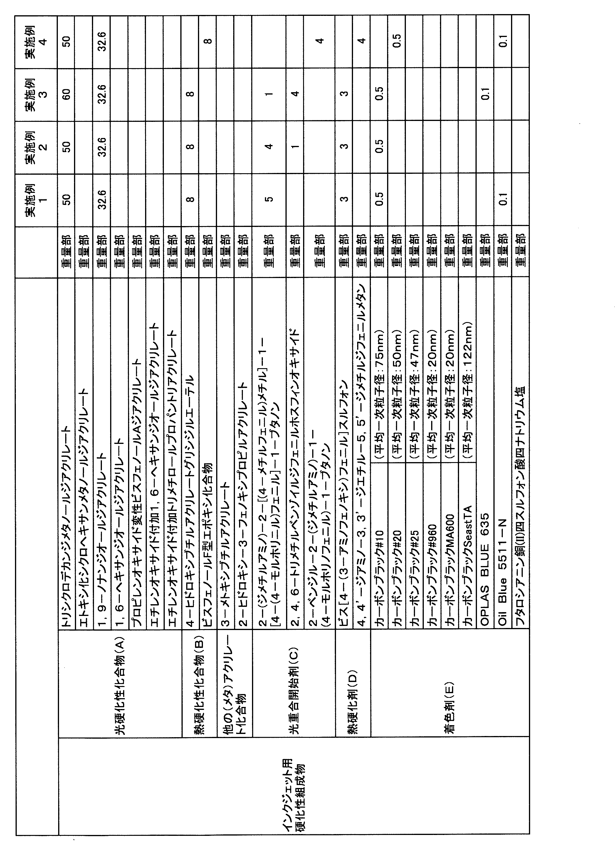
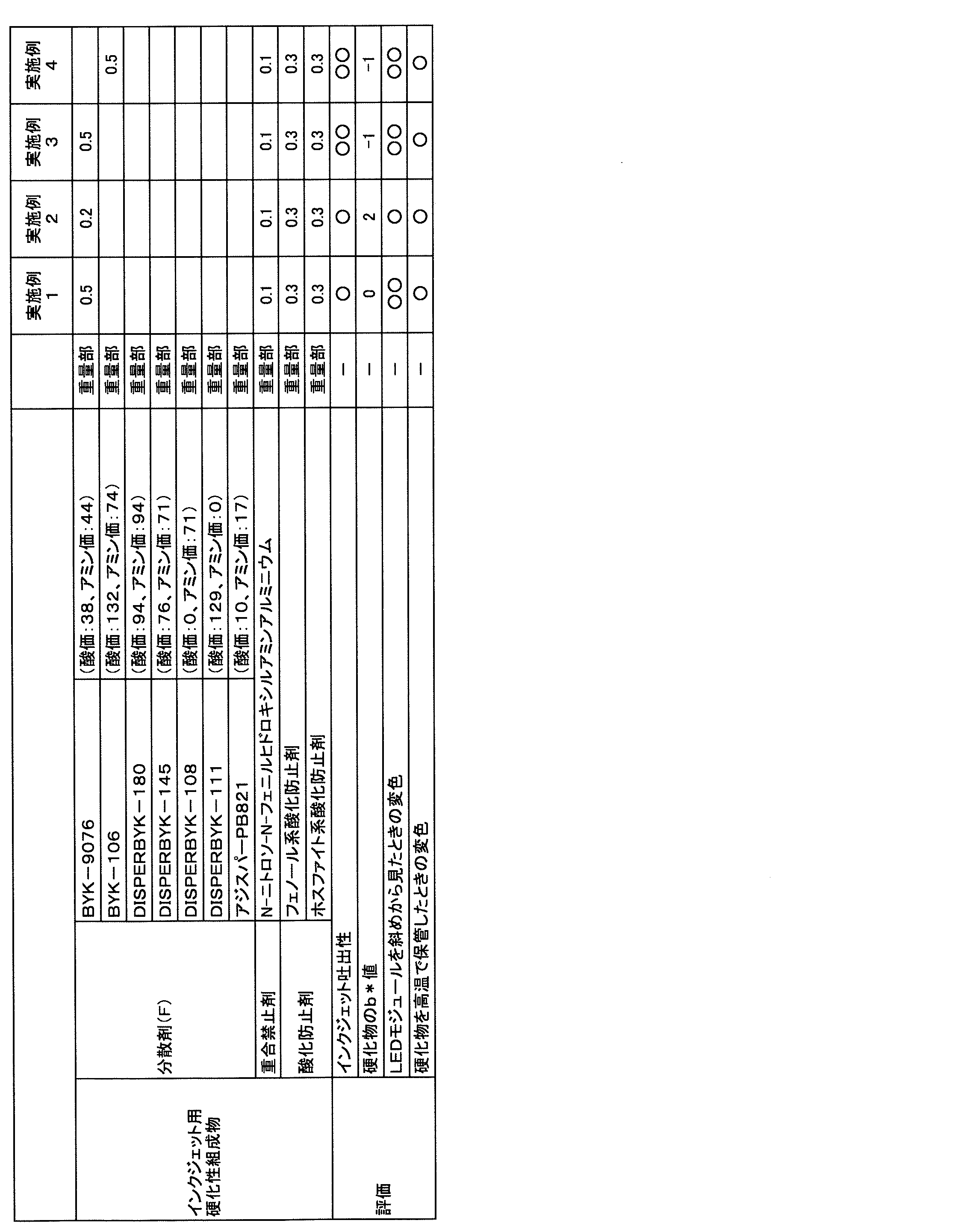
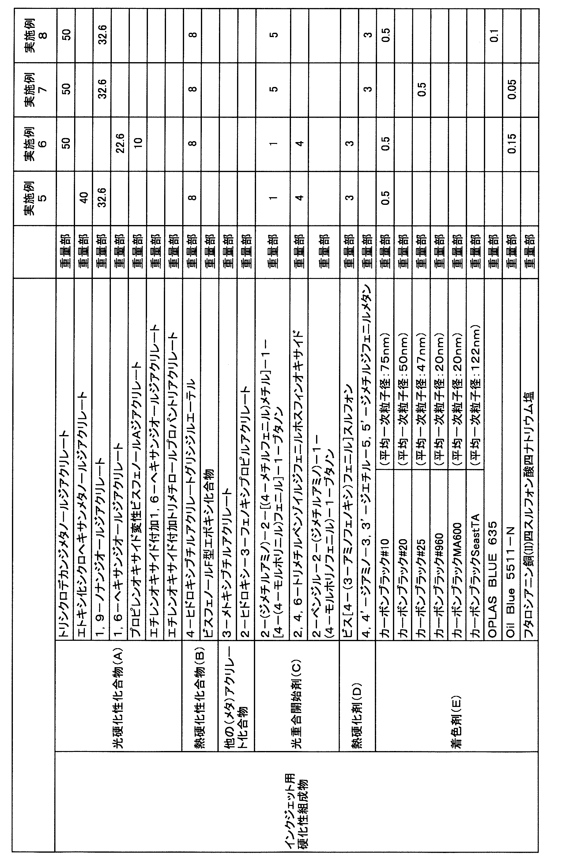
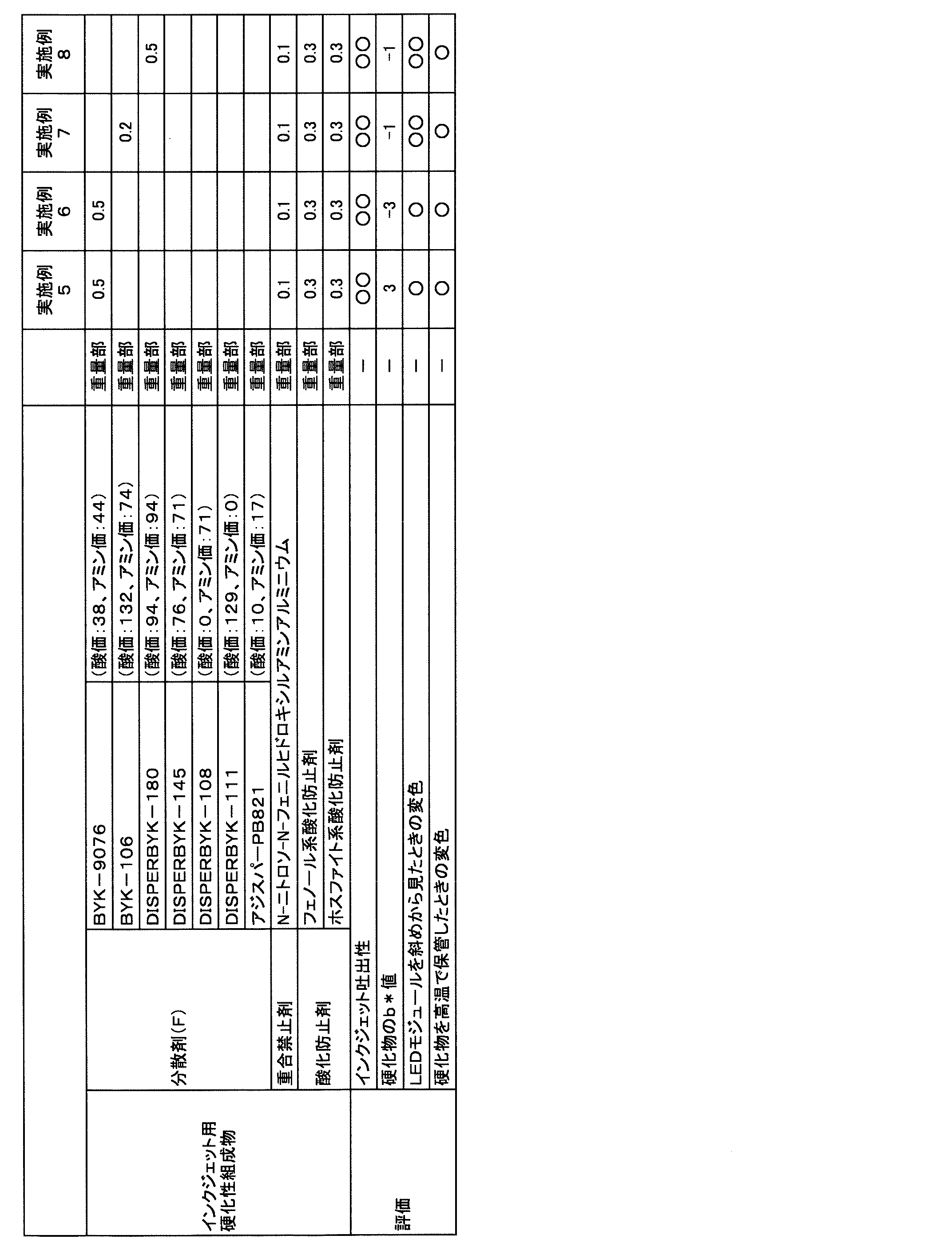
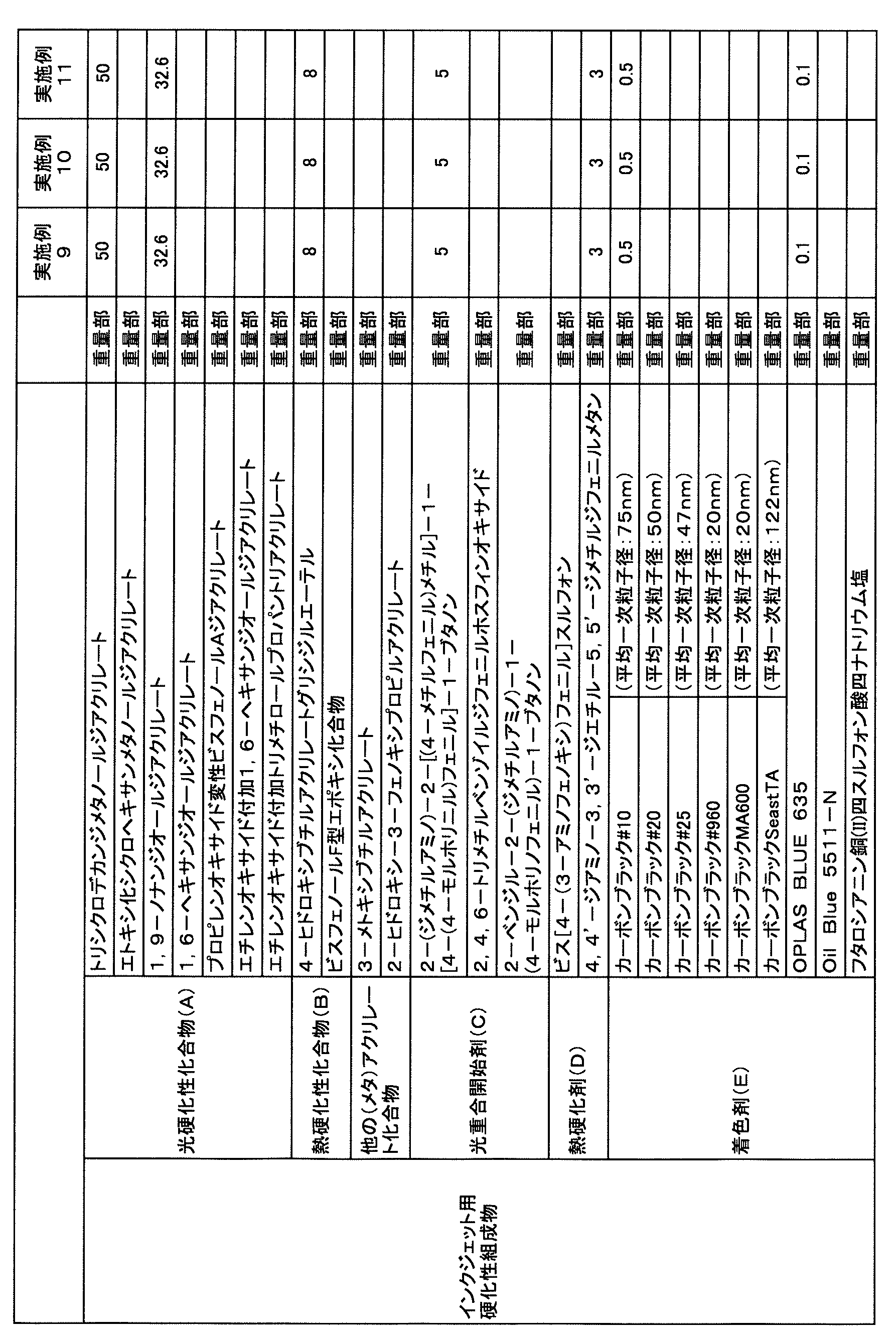

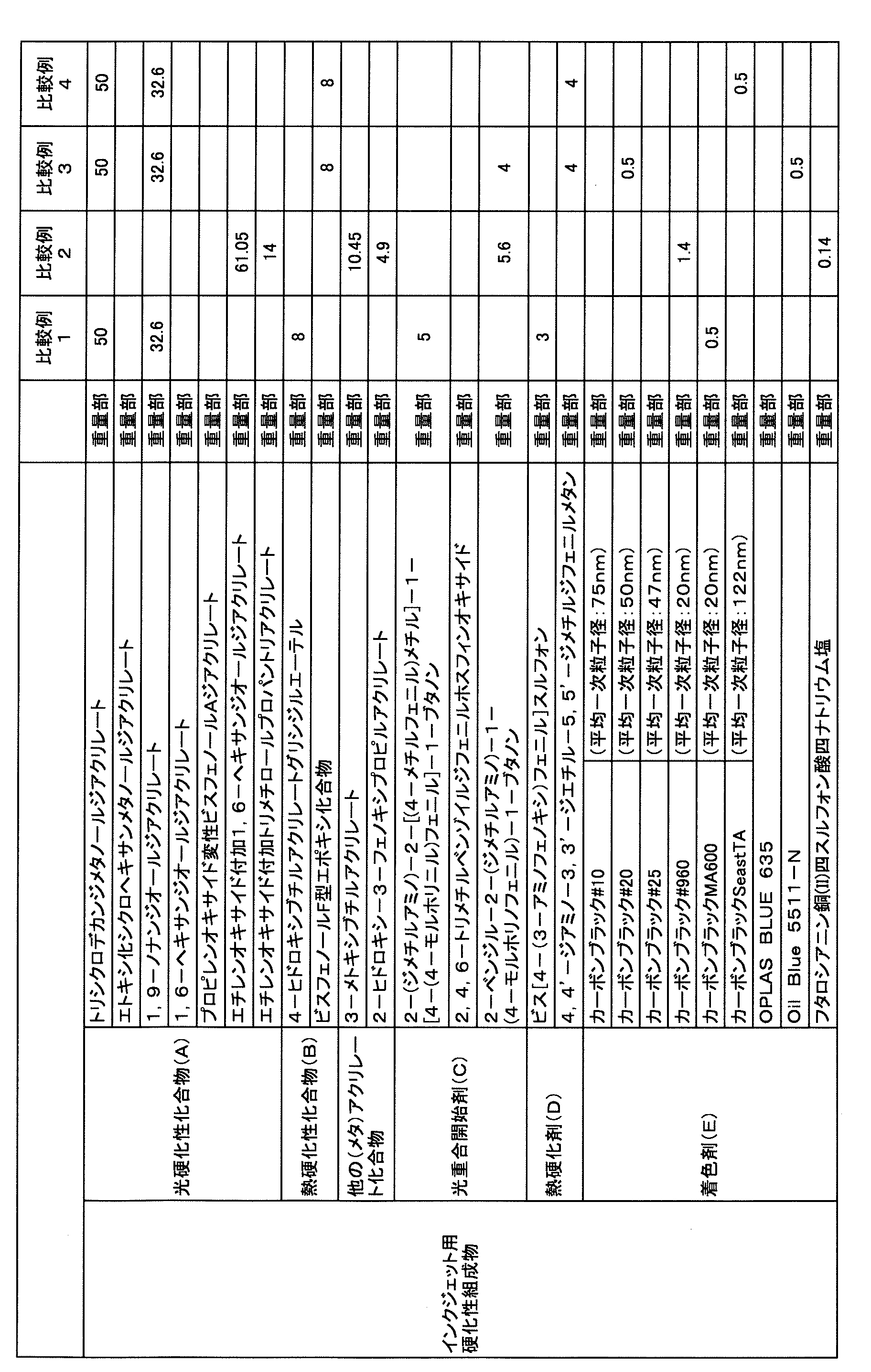


11…基板
12…LEDチップ
13…隔壁
13A…組成物層
13B…Bステージ化物
15…表面層
16…光透過層
51…吐出部
52…光照射部
Claims (11)
- 光重合性官能基を2個以上有し、かつ環状エーテル基を有さない光硬化性化合物と、
環状エーテル基を有する熱硬化性化合物と、
光重合開始剤と、
熱硬化剤と、
着色剤と、
分散剤とを含むインクジェット用硬化性組成物であり、
前記着色剤が、カーボンブラックを含み、
前記カーボンブラックの平均粒子径が、40nm以上100nm以下であり、
厚み30μmの前記インクジェット用硬化性組成物の硬化物について、前記硬化物に光を照射したときに、前記硬化物の反射光のL*a*b*表色系におけるb*値が、-3以上3以下である、インクジェット用硬化性組成物。 - 前記分散剤の酸価が10mgKOH/g以上150mgKOH/g以下であり、かつ、前記分散剤のアミン価が10mgKOH/g以上100mgKOH/g以下である、請求項1に記載のインクジェット用硬化性組成物。
- 前記光重合開始剤が、アミノアセトフェノン化合物を含む、請求項1又は2に記載のインクジェット用硬化性組成物。
- 前記インクジェット用硬化性組成物100重量%中、前記カーボンブラックの含有量が、0.1重量%以上5.0重量%以下である、請求項1~3のいずれか1項に記載のインクジェット用硬化性組成物。
- 前記着色剤が、カーボンブラック以外の着色剤をさらに含む、請求項1~4のいずれか1項に記載のインクジェット用硬化性組成物。
- 前記着色剤が、フタロシアニン化合物をさらに含む、請求項1~5のいずれか1項に記載のインクジェット用硬化性組成物。
- 前記光硬化性化合物が、(メタ)アクリロイル基を2個以上有し、かつジシクロペンタジエン骨格を有する光硬化性化合物を含む、請求項1~6のいずれか1項に記載のインクジェット用硬化性組成物。
- 前記熱硬化性化合物が、4-ヒドロキシブチル(メタ)アクリレートグリシジルエーテルを含む、請求項1~7のいずれか1項に記載のインクジェット用硬化性組成物。
- LEDモジュールにおいて隔壁を形成するために用いられる、請求項1~8のいずれか1項に記載のインクジェット用硬化性組成物。
- 基板と、
前記基板の第1の表面上に配置されたLEDチップと、
前記基板の前記第1の表面上に配置された隔壁とを備え、
前記隔壁が、前記基板の前記第1の表面上にて、前記LEDチップを囲むように配置されており、
前記隔壁が、請求項1~9のいずれか1項に記載のインクジェット用硬化性組成物の硬化物である、LEDモジュール。 - 基板の第1の表面上に、請求項1~9のいずれか1項に記載のインクジェット用硬化性組成物をインクジェット方式で塗布して、組成物層を形成する塗布工程と、
塗布された前記インクジェット用硬化性組成物に光を照射して、前記インクジェット用硬化性組成物を硬化させて、Bステージ化物を形成する光硬化工程と、
加熱により前記Bステージ化物を熱硬化させて隔壁を形成する熱硬化工程と、
前記基板の前記第1の表面上かつ前記隔壁で囲まれた領域の内側に、LEDチップを配置する工程とを備える、LEDモジュールの製造方法。
Priority Applications (3)
| Application Number | Priority Date | Filing Date | Title |
|---|---|---|---|
| CN202380072108.9A CN120021422A (zh) | 2022-11-10 | 2023-11-07 | 喷墨用固化性组合物、led模块及led模块的制造方法 |
| KR1020257008995A KR20250105602A (ko) | 2022-11-10 | 2023-11-07 | 잉크젯용 경화성 조성물, led 모듈 및 led 모듈의 제조 방법 |
| JP2024557425A JPWO2024101359A1 (ja) | 2022-11-10 | 2023-11-07 |
Applications Claiming Priority (2)
| Application Number | Priority Date | Filing Date | Title |
|---|---|---|---|
| JP2022180604 | 2022-11-10 | ||
| JP2022-180604 | 2022-11-10 |
Publications (1)
| Publication Number | Publication Date |
|---|---|
| WO2024101359A1 true WO2024101359A1 (ja) | 2024-05-16 |
Family
ID=91032445
Family Applications (1)
| Application Number | Title | Priority Date | Filing Date |
|---|---|---|---|
| PCT/JP2023/040071 Ceased WO2024101359A1 (ja) | 2022-11-10 | 2023-11-07 | インクジェット用硬化性組成物、ledモジュール、及びledモジュールの製造方法 |
Country Status (5)
| Country | Link |
|---|---|
| JP (1) | JPWO2024101359A1 (ja) |
| KR (1) | KR20250105602A (ja) |
| CN (1) | CN120021422A (ja) |
| TW (1) | TW202421731A (ja) |
| WO (1) | WO2024101359A1 (ja) |
Citations (5)
| Publication number | Priority date | Publication date | Assignee | Title |
|---|---|---|---|---|
| JP2014191281A (ja) * | 2013-03-28 | 2014-10-06 | Tdk Corp | 光電気混載基板 |
| JP2016196579A (ja) * | 2015-04-03 | 2016-11-24 | 積水化学工業株式会社 | インクジェット用マーキング材料、電子部品の製造方法及び電子部品 |
| JP2020182948A (ja) * | 2014-10-24 | 2020-11-12 | Agc株式会社 | 隔壁の修復方法、修復された隔壁、および光学素子 |
| JP2020205417A (ja) * | 2019-06-12 | 2020-12-24 | 東レ株式会社 | マイクロledディスプレイ装置 |
| JP2022135603A (ja) * | 2021-03-05 | 2022-09-15 | 積水化学工業株式会社 | インクジェット塗布用及びled用硬化性組成物、ledモジュール、ledモジュールの製造方法及びled表示装置 |
Family Cites Families (1)
| Publication number | Priority date | Publication date | Assignee | Title |
|---|---|---|---|---|
| JP7067269B6 (ja) | 2018-05-24 | 2023-12-20 | 大日本印刷株式会社 | 自発光型表示体 |
-
2023
- 2023-11-07 JP JP2024557425A patent/JPWO2024101359A1/ja active Pending
- 2023-11-07 WO PCT/JP2023/040071 patent/WO2024101359A1/ja not_active Ceased
- 2023-11-07 KR KR1020257008995A patent/KR20250105602A/ko active Pending
- 2023-11-07 CN CN202380072108.9A patent/CN120021422A/zh active Pending
- 2023-11-09 TW TW112143170A patent/TW202421731A/zh unknown
Patent Citations (5)
| Publication number | Priority date | Publication date | Assignee | Title |
|---|---|---|---|---|
| JP2014191281A (ja) * | 2013-03-28 | 2014-10-06 | Tdk Corp | 光電気混載基板 |
| JP2020182948A (ja) * | 2014-10-24 | 2020-11-12 | Agc株式会社 | 隔壁の修復方法、修復された隔壁、および光学素子 |
| JP2016196579A (ja) * | 2015-04-03 | 2016-11-24 | 積水化学工業株式会社 | インクジェット用マーキング材料、電子部品の製造方法及び電子部品 |
| JP2020205417A (ja) * | 2019-06-12 | 2020-12-24 | 東レ株式会社 | マイクロledディスプレイ装置 |
| JP2022135603A (ja) * | 2021-03-05 | 2022-09-15 | 積水化学工業株式会社 | インクジェット塗布用及びled用硬化性組成物、ledモジュール、ledモジュールの製造方法及びled表示装置 |
Also Published As
| Publication number | Publication date |
|---|---|
| JPWO2024101359A1 (ja) | 2024-05-16 |
| KR20250105602A (ko) | 2025-07-08 |
| CN120021422A (zh) | 2025-05-20 |
| TW202421731A (zh) | 2024-06-01 |
Similar Documents
| Publication | Publication Date | Title |
|---|---|---|
| TWI884058B (zh) | 含有量子點之硬化性組成物、含有量子點之硬化物、光學構件之製造方法及顯示裝置之製造方法 | |
| CN117460795A (zh) | 喷墨用及隔壁形成用固化性组合物、发光设备及发光设备的制造方法 | |
| US12528956B2 (en) | Ink-jet adhesive, method for producing electronic component, and electronic component | |
| TW201619296A (zh) | 硬化性樹脂組成物、乾薄膜、硬化物及印刷電路板 | |
| JP6329100B2 (ja) | インクジェット用マーキング材料、電子部品の製造方法及び電子部品 | |
| TWI771575B (zh) | 壓印用下層膜形成組成物、套組、壓印用硬化性組成物、積層體、積層體的製造方法、圖案形成方法及半導體器件的製造方法 | |
| JP2022135603A (ja) | インクジェット塗布用及びled用硬化性組成物、ledモジュール、ledモジュールの製造方法及びled表示装置 | |
| WO2024101359A1 (ja) | インクジェット用硬化性組成物、ledモジュール、及びledモジュールの製造方法 | |
| TW202004336A (zh) | 硬化性樹脂組成物、乾薄膜、硬化物及印刷配線板 | |
| WO2024172153A1 (ja) | インクジェット用硬化性組成物及び電子部品 | |
| JP2024070162A (ja) | インクジェット用及びled保護用硬化性組成物、ledモジュール、ledモジュールの製造方法、及びled表示装置 | |
| JP2024046641A (ja) | インクジェット用マーキング材料、電子部品、及び電子部品の製造方法 | |
| TW202219203A (zh) | 噴墨塗布用及led保護用硬化性組合物、led模組、led模組之製造方法及led顯示裝置 | |
| WO2024204095A1 (ja) | 隔壁形成用インクジェット組成物、ledモジュール及びledモジュールの製造方法 | |
| KR102773964B1 (ko) | 경화성 투명 수지 조성물 및 이로부터 유도된 각종 물품 | |
| KR102773970B1 (ko) | 경화성 투명 수지 조성물 및 이로부터 유도된 각종 물품 | |
| TWI889848B (zh) | 阻隔壁用硬化性組合物、阻隔壁之修復方法、阻隔壁、及光學元件 | |
| WO2026063522A1 (ja) | インクジェット用硬化性組成物、電子部品及び電子部品の製造方法 | |
| WO2024204093A1 (ja) | 隔壁形成用インクジェット組成物、ledモジュール及びledモジュールの製造方法 | |
| TW202003650A (zh) | 乾薄膜、硬化物及印刷配線板 | |
| KR102883567B1 (ko) | 적층 구조체의 제조 방법, 적층 구조체, 및 잉크젯용 조성물 세트 | |
| TW202602958A (zh) | 感光性樹脂組成物、乾膜、硬化物及印刷配線基板 | |
| WO2024080336A1 (ja) | インクジェット用及びエアキャビティ形成用硬化性組成物、及び電子部品 | |
| TWI771311B (zh) | 扇出型的晶圓級封裝之製造方法 | |
| JP2024179393A (ja) | インク組成物、硬化物及び画像表示装置 |
Legal Events
| Date | Code | Title | Description |
|---|---|---|---|
| 121 | Ep: the epo has been informed by wipo that ep was designated in this application |
Ref document number: 23888706 Country of ref document: EP Kind code of ref document: A1 |
|
| WWE | Wipo information: entry into national phase |
Ref document number: 2024557425 Country of ref document: JP |
|
| WWE | Wipo information: entry into national phase |
Ref document number: 202380072108.9 Country of ref document: CN |
|
| WWP | Wipo information: published in national office |
Ref document number: 202380072108.9 Country of ref document: CN |
|
| NENP | Non-entry into the national phase |
Ref country code: DE |
|
| WWP | Wipo information: published in national office |
Ref document number: 1020257008995 Country of ref document: KR |
|
| 122 | Ep: pct application non-entry in european phase |
Ref document number: 23888706 Country of ref document: EP Kind code of ref document: A1 |