WO2024095931A1 - レンズアレイ - Google Patents
レンズアレイ Download PDFInfo
- Publication number
- WO2024095931A1 WO2024095931A1 PCT/JP2023/038981 JP2023038981W WO2024095931A1 WO 2024095931 A1 WO2024095931 A1 WO 2024095931A1 JP 2023038981 W JP2023038981 W JP 2023038981W WO 2024095931 A1 WO2024095931 A1 WO 2024095931A1
- Authority
- WO
- WIPO (PCT)
- Prior art keywords
- lens
- lens array
- reflection film
- binder
- lenses
- Prior art date
- Legal status (The legal status is an assumption and is not a legal conclusion. Google has not performed a legal analysis and makes no representation as to the accuracy of the status listed.)
- Ceased
Links
Images





Classifications
-
- G—PHYSICS
- G02—OPTICS
- G02B—OPTICAL ELEMENTS, SYSTEMS OR APPARATUS
- G02B3/00—Simple or compound lenses
- G02B3/0006—Arrays
-
- C—CHEMISTRY; METALLURGY
- C03—GLASS; MINERAL OR SLAG WOOL
- C03C—CHEMICAL COMPOSITION OF GLASSES, GLAZES OR VITREOUS ENAMELS; SURFACE TREATMENT OF GLASS; SURFACE TREATMENT OF FIBRES OR FILAMENTS MADE FROM GLASS, MINERALS OR SLAGS; JOINING GLASS TO GLASS OR OTHER MATERIALS
- C03C3/00—Glass compositions
- C03C3/04—Glass compositions containing silica
- C03C3/076—Glass compositions containing silica with 40% to 90% silica, by weight
- C03C3/078—Glass compositions containing silica with 40% to 90% silica, by weight containing an oxide of a divalent metal, e.g. an oxide of zinc
-
- C—CHEMISTRY; METALLURGY
- C03—GLASS; MINERAL OR SLAG WOOL
- C03C—CHEMICAL COMPOSITION OF GLASSES, GLAZES OR VITREOUS ENAMELS; SURFACE TREATMENT OF GLASS; SURFACE TREATMENT OF FIBRES OR FILAMENTS MADE FROM GLASS, MINERALS OR SLAGS; JOINING GLASS TO GLASS OR OTHER MATERIALS
- C03C3/00—Glass compositions
- C03C3/04—Glass compositions containing silica
- C03C3/076—Glass compositions containing silica with 40% to 90% silica, by weight
- C03C3/083—Glass compositions containing silica with 40% to 90% silica, by weight containing aluminium oxide or an iron compound
- C03C3/085—Glass compositions containing silica with 40% to 90% silica, by weight containing aluminium oxide or an iron compound containing an oxide of a divalent metal
-
- C—CHEMISTRY; METALLURGY
- C03—GLASS; MINERAL OR SLAG WOOL
- C03C—CHEMICAL COMPOSITION OF GLASSES, GLAZES OR VITREOUS ENAMELS; SURFACE TREATMENT OF GLASS; SURFACE TREATMENT OF FIBRES OR FILAMENTS MADE FROM GLASS, MINERALS OR SLAGS; JOINING GLASS TO GLASS OR OTHER MATERIALS
- C03C3/00—Glass compositions
- C03C3/04—Glass compositions containing silica
- C03C3/076—Glass compositions containing silica with 40% to 90% silica, by weight
- C03C3/089—Glass compositions containing silica with 40% to 90% silica, by weight containing boron
-
- C—CHEMISTRY; METALLURGY
- C03—GLASS; MINERAL OR SLAG WOOL
- C03C—CHEMICAL COMPOSITION OF GLASSES, GLAZES OR VITREOUS ENAMELS; SURFACE TREATMENT OF GLASS; SURFACE TREATMENT OF FIBRES OR FILAMENTS MADE FROM GLASS, MINERALS OR SLAGS; JOINING GLASS TO GLASS OR OTHER MATERIALS
- C03C3/00—Glass compositions
- C03C3/04—Glass compositions containing silica
- C03C3/076—Glass compositions containing silica with 40% to 90% silica, by weight
- C03C3/089—Glass compositions containing silica with 40% to 90% silica, by weight containing boron
- C03C3/091—Glass compositions containing silica with 40% to 90% silica, by weight containing boron containing aluminium
- C03C3/093—Glass compositions containing silica with 40% to 90% silica, by weight containing boron containing aluminium containing zinc or zirconium
-
- C—CHEMISTRY; METALLURGY
- C03—GLASS; MINERAL OR SLAG WOOL
- C03C—CHEMICAL COMPOSITION OF GLASSES, GLAZES OR VITREOUS ENAMELS; SURFACE TREATMENT OF GLASS; SURFACE TREATMENT OF FIBRES OR FILAMENTS MADE FROM GLASS, MINERALS OR SLAGS; JOINING GLASS TO GLASS OR OTHER MATERIALS
- C03C3/00—Glass compositions
- C03C3/04—Glass compositions containing silica
- C03C3/076—Glass compositions containing silica with 40% to 90% silica, by weight
- C03C3/095—Glass compositions containing silica with 40% to 90% silica, by weight containing rare earths
-
- C—CHEMISTRY; METALLURGY
- C03—GLASS; MINERAL OR SLAG WOOL
- C03C—CHEMICAL COMPOSITION OF GLASSES, GLAZES OR VITREOUS ENAMELS; SURFACE TREATMENT OF GLASS; SURFACE TREATMENT OF FIBRES OR FILAMENTS MADE FROM GLASS, MINERALS OR SLAGS; JOINING GLASS TO GLASS OR OTHER MATERIALS
- C03C3/00—Glass compositions
- C03C3/04—Glass compositions containing silica
- C03C3/076—Glass compositions containing silica with 40% to 90% silica, by weight
- C03C3/097—Glass compositions containing silica with 40% to 90% silica, by weight containing phosphorus, niobium or tantalum
-
- G—PHYSICS
- G02—OPTICS
- G02B—OPTICAL ELEMENTS, SYSTEMS OR APPARATUS
- G02B1/00—Optical elements characterised by the material of which they are made; Optical coatings for optical elements
-
- G—PHYSICS
- G02—OPTICS
- G02B—OPTICAL ELEMENTS, SYSTEMS OR APPARATUS
- G02B1/00—Optical elements characterised by the material of which they are made; Optical coatings for optical elements
- G02B1/10—Optical coatings produced by application to, or surface treatment of, optical elements
- G02B1/11—Anti-reflection coatings
- G02B1/111—Anti-reflection coatings using layers comprising organic materials
-
- G—PHYSICS
- G02—OPTICS
- G02B—OPTICAL ELEMENTS, SYSTEMS OR APPARATUS
- G02B3/00—Simple or compound lenses
Definitions
- the present invention relates to a lens array.
- lens arrays are used for image reading.
- Patent Document 1 describes a laminated lens array unit for a compound eye optical system.
- This laminated lens array unit includes a first lens array, a second lens array, and a positioning unit.
- Each of the first lens array and the second lens array has a rectangular outline when viewed from the optical axis direction, and has a plurality of lens elements arranged two-dimensionally.
- the first lens array and the second lens array are stacked in the optical axis direction.
- the positioning unit is provided in an enclosing area that surrounds the plurality of lens elements along the edge of the first lens array and the edge of the second lens array.
- the positioning unit has a first abutment portion arranged on the first lens array side, and a second abutment portion arranged on the second lens array side and facing the first abutment portion, and has a predetermined tapered surface.
- This makes it possible to regulate the planar direction and the rotational direction around the axis perpendicular to the planar direction required for the lens array without applying stress to the lens array. Therefore, assembly can be performed with high precision while maintaining high optical performance.
- the structure between adjacent lens elements in the lens array can be simplified, allowing for high-precision molding and making it easier to ensure a wide effective area for the lens elements.
- the lens array unit described in Patent Document 1 is not expected to be used in equipment that inspects for defects using reflected light from transported objects. When using a lens array in such equipment, it is considered to be advantageous for the lens array to be compatible with various measurement wavelengths, depending on the object being inspected.
- the present invention provides a lens array that is advantageous in terms of the range of measurement wavelengths that can be handled by equipment that inspects for defects using reflected light from transported objects to be inspected.
- the present invention relates to A lens array used in an apparatus for inspecting the presence or absence of defects by using reflected light from an object being transported, a plurality of lenses arranged in a first direction that is a transport direction of the object to be inspected and in a second direction perpendicular to the transport direction, the lenses focusing the reflected light;
- An adhesive portion that fixes the lenses together;
- a housing that houses the lenses and the adhesive portion;
- the antireflection film includes fine particles having a refractive index equal to or lower than that of the lens, and a binder, and is disposed in contact with at least one surface selected from the group consisting of a first surface of the lens onto which the reflected light is incident and a second surface of the lens from which the light incident on the first surface is emitted,
- the binder adheres the particulates to the first surface or the second surface.
- a lens array is provided.
- the lens array described above is advantageous in terms of the range of measurement wavelengths that can be handled by equipment that inspects for defects using reflected light from transported objects to be inspected.
- FIG. 1 is a schematic perspective view showing an example of a lens array according to the present invention.
- FIG. 2 is a graph showing the refractive index distribution of a lens.
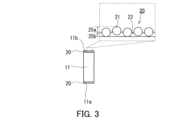
- FIG. 3 is a side view showing an example of the lens shown in FIG.
- FIG. 4 is a cross-sectional view showing an example of an inspection device including the lens array shown in FIG.
- FIG. 5A is an FE-SEM photograph showing a cross section of the antireflection film of the lens array according to Example 1.
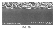
- FIG. 5B is an FE-SEM photograph showing a cross section of the antireflection film of the lens array according to Example 6.
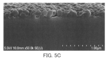
- FIG. 5C is an FE-SEM photograph showing a cross section of the antireflection film of the lens array according to Example 7.
- FIG. 6 is a cross-sectional view illustrating a cross section of an anti-reflection film of a lens array according to an eighth embodiment.
- the lens array 1a includes a plurality of lenses 11, an adhesive portion 12, and a housing 15.
- the lens array 1a is used in an apparatus that inspects the presence or absence of defects by using reflected light from an object being transported.
- the lenses 11 are arranged in a first direction (y-axis direction) that is the transport direction of the object being transported, and a second direction (x-axis direction) perpendicular to the transport direction.
- the lenses 11 focus the reflected light from the object being transported.
- the adhesive portion 12 fixes the lenses 11 together.
- the housing 15 houses the lenses 11 and the adhesive portion 12.
- the lenses 11 have a working distance L 1 of, for example, 5 mm or more.
- Lens arrays are often used for image reading and other purposes.
- a lens array is used in a device that inspects the presence or absence of defects using reflected light from a transported object to be inspected, foreign matter originating from the transported object to be inspected is likely to adhere to the surface of the lens array. For this reason, such devices may require regular or irregular maintenance of the device. In this case, if the distance between the lens array and the object to be inspected is small, it is difficult to ensure sufficient space for equipment maintenance.
- the lens 11 has a working distance of 5 mm or more. For this reason, when the lens array 1a is used in a device that inspects the presence or absence of defects using reflected light from a transported object to be inspected, the distance between the lens array 1a and the object to be inspected is likely to be large, and sufficient space for equipment maintenance is likely to be ensured.
- the working distance L1 of the lens 11 is preferably 8 mm or more, more preferably 10 mm or more, even more preferably 15 mm or more, particularly preferably 20 mm or more, and particularly preferably 25 mm or more.
- the working distance L1 is, for example, 60 mm or less, may be 55 mm or less, or may be 50 mm or less.
- the lens 11 is, for example, a gradient index lens.
- OP is an object plane
- IP is an image plane
- TC is a conjugate length
- Z is a lens length
- X0 is a field radius
- ⁇ C is an aperture angle.
- L0 is the distance between the image plane IP and the lens 11 when the value of the modulation transfer function (MTF) is maximum.
- the lens array 1a constitutes, for example, a substantially erect life-size imaging system, and the working distance L1 is substantially equal to the distance L0 .
- the conjugate length TC is, for example, 35 mm to 160 mm, preferably 40 mm to 150 mm, and more preferably 48 mm to 100 mm.
- the relationship TC L 1 +Z+L 0 holds.
- the aperture angle ⁇ C is, for example, 3° to 22°, and preferably 4° to 12°.
- the lens 11 is, for example, a rod lens, and the central axis of the lens 11 extends in the optical axis direction of the lens 11. As shown in Fig. 2, the lens 11 has a refractive index distribution in its radial direction.
- n0 is the refractive index at the central axis of the lens 11
- r is the distance [mm] from the central axis of the lens 11 in the radial direction of the lens 11.
- the refractive index n(r) of the lens 11 at the distance r is expressed by the following formula (1).
- g is the refractive index distribution constant [mm -1 ] of the lens 11.
- n(r) 2 n 0 2 ⁇ 1 - (g ⁇ r) 2 ⁇ Equation (1)
- the refractive index distribution constant of the lens 11 is, for example, 0.06 mm -1 to 0.48 mm -1 , and preferably 0.08 mm -1 to 0.26 mm -1 .
- the lens 11 may be made of resin or glass.
- the resin forming the lens 11 include light-transmitting acrylic resin, polycarbonate resin, polyolefin resin, and silicone resin.
- the center of the lens 11 has, for example, the following composition.
- the working distance L1 tends to be large, and the working distance L1 tends to be a desired value.
- the center of the lens 11 is, for example, a portion that forms the optical axis of the lens 11.
- the lens 11 can be produced, for example, by a method including the following steps (I) and (II).
- a glass wire having the above composition is prepared.
- a glass wire is immersed in a molten salt containing a second alkali metal element R different from the first alkali metal element Q contained in the above composition, and an ion exchange treatment is performed between the first alkali metal element Q in the glass wire and the second alkali metal element R in the molten salt, thereby forming a refractive index distribution in the glass wire.
- step (II) for example, the glass wire is placed in the molten salt inside the container and immersed in the molten salt for a predetermined time.
- the molten salt for example, at least one of potassium nitrate and sodium nitrate is melted.
- the cations of the first alkali metal element Q such as Li (lithium)
- the cations of the second alkali metal element R such as Na (sodium)
- the ion exchange between the cations of the first alkali metal element Q and the cations of the second alkali metal element R can be appropriately controlled.
- a concentration distribution of specific monovalent cations occurs inside the glass wire, and a lens 11 having a refractive index distribution as shown in FIG. 2 is obtained according to this concentration distribution. Note that almost no ion exchange occurs in the center of the glass wire, so the center of the lens 11 has the initial composition of the glass wire. Therefore, the center of the lens 11 has the above composition.
- the lenses 11 are arranged in a plurality of rows in the second direction (x-axis direction), for example.
- the number of rows of the lenses 11 formed in the second direction may be two, or may be three or more.
- the rows of the lenses 11 adjacent to each other in the first direction are formed such that the central axes of the lenses 11 are shifted in the second direction, for example.
- the adhesive portion 12 fills the gaps between the lenses 11. This integrates the lenses 11 together.
- the adhesive portion 12 contains, for example, a resin and is colored black.
- the housing 15 is not limited to a specific configuration as long as it can accommodate multiple lenses 11 and adhesive parts 12.
- the housing 15 includes, for example, a pair of plate materials aligned in a first direction and a pair of plate materials aligned in a second direction, and is formed as a frame made of these plate materials.
- plate materials include, for example, fiber reinforced plastic (FRP).
- the lens array 1a further includes, for example, an anti-reflection film 20.
- the anti-reflection film 20 is arranged, for example, in contact with at least one selected from the group consisting of the first surface 11a and the second surface 11b.
- the first surface 11a is the surface of the lens 11 on which reflected light from an object being transported is incident.
- the second surface 11b is the surface of the lens 11 from which the light incident on the first surface 11a is emitted.
- the working distance L 1 of the lens 11 is 5 mm or more, the image obtained by the lens 11 is not likely to be bright, and the amount of light incident on an imaging element such as a Charge Coupled Device (CCD) used in the above-mentioned device to inspect the presence or absence of defects in the object to be inspected is likely to be low.
- CCD Charge Coupled Device
- the brightness may decrease by about 30%. Therefore, for example, it is possible to increase the brightness of the light source for generating reflected light from the object to be inspected.
- the lens array 1a is provided with the anti-reflection film 20, the reflected light from the object to be inspected is suppressed from being re-reflected on the first surface 11a and the second surface 11b of the lens 11. As a result, even if the brightness of the light source is not increased, a bright image is easily obtained by the lens 11, and the amount of light incident on the imaging element is unlikely to be low.
- the anti-reflection film 20 may be disposed in contact with only the first surface 11a, may be disposed in contact with only the second surface 11b, or may be disposed in contact with both the first surface 11a and the second surface 11b.
- the anti-reflection film 20 is not limited to a specific form, so long as it can increase the amount of light emitted from the second surface 11b compared to a case in which the anti-reflection film 20 is not formed.
- the anti-reflection film 20 includes fine particles 21 and a binder 22, as shown in FIG. 3.
- the fine particles 21 have a refractive index equal to or lower than that of the lens 11.
- the refractive index of the lens 11 is the maximum value of the refractive index of the lens 11, for example, the refractive index at the center of the lens 11.
- the binder 22 bonds the fine particles 21 to the first surface 11a or the second surface 11b.
- the desired anti-reflection characteristics are likely to be exhibited not only when the measurement wavelength belongs to the visible light region but also when the measurement wavelength belongs to the near-infrared region, and the amount of light emitted from the second surface 11b can be increased.
- the anti-reflection film 20 is likely to exhibit the desired anti-reflection characteristics even if it is formed to have a relatively simple structure such as a single layer structure.
- a vacuum process or high-temperature treatment is not required, which can prevent the influence of such processes or treatments on the lens 11, and the manufacturing cost of the lens array 1a is likely to be low.
- One possible method for forming an anti-reflection coating on a lens is to form an optical interference film, which is a dielectric multilayer film, by methods such as vacuum deposition, sputtering, and chemical vapor deposition (CVD).
- an optical interference film which is a dielectric multilayer film
- CVD chemical vapor deposition
- the reflectance increases rapidly outside the design wavelength range, and there is a limit to the anti-reflection effect over a wide wavelength range.
- this method requires processing such as a vacuum process or heating at high temperatures, and there is a possibility that the resin contained in the lens array 1a may foam during the vacuum process. For this reason, it is difficult to say that it is realistic to form a dielectric optical interference film as an anti-reflection coating on the lens 11.
- the surface layer of the anti-reflection film 20 is unevenly formed by the fine particles 21. This forms a low refractive index portion 25a that has a refractive index lower than that of the lens 11. With this configuration, the anti-reflection film 20 is more likely to exhibit the desired anti-reflection characteristics over a wide wavelength range.
- the anti-reflection film 20 includes, for example, a base 25b between the low refractive index portion 25a and the lens 11 in the thickness direction of the anti-reflection film 20.
- the binder 22 forms a layer between the fine particles 21 in the base 25b.
- the low refractive index portion 25a is a portion of the anti-reflection film 20 other than the base 25b.
- the content of the binder 22 in the base 25b is higher than the content of the binder 22 in the low refractive index portion 25a on a mass basis. This makes it easier for the anti-reflection film 20 to exhibit the desired anti-reflection performance, and the anti-reflection film 20 is less likely to peel off from the lens 11.
- the anti-reflection film 20 may come into contact with other objects.
- the content of the binder 22 in the base 25 is higher than the content of the binder 22 in the low refractive index portion 25a, the bonding strength of the anti-reflection film 20 to the lens 11 is likely to be high.
- the anti-reflection film 20 contains, for example, silicon atoms, and between the anti-reflection film 20 and the lens 11, bonds involving silicon atoms, such as Si-O-Si bonds, are formed. With this configuration, the bonding strength of the anti-reflection film 20 to the lens 11 is likely to be higher. If the lens 11 is made of glass, silanol groups may be present on the surface of the lens 11. Therefore, a condensation reaction between the silanol groups on the surface of the lens 11 and the silanol groups contained in the anti-reflection film 20 may form bonds involving silicon atoms, such as Si-O-Si bonds. If the lens 11 is made of resin, the surface of the lens 11 may be treated with a primer. As a result, bonds involving silicon atoms, such as Si-O-Si bonds, may be formed between the lens 11 and the anti-reflection film 20.
- the components contained in the microparticles 21 are not limited to a specific component.
- the microparticles 21 are mainly composed of silica, for example.
- the main component is the component that is contained in the largest amount by mass. Bonds involving silicon atoms, such as Si-O-Si bonds, are formed between the microparticles 21 and the binder 22. With this configuration, the bonding strength of the anti-reflection film 20 to the lens 11 is likely to be higher. The bonding strength between the microparticles 21 and the binder 22 is higher, and the microparticles 21 are less likely to come off the anti-reflection film 20. As a result, the bonding strength of the anti-reflection film 20 to the lens 11 is likely to be higher.
- the average particle size of the particles 21 is not limited to a specific value.
- the average particle size of the particles 21 is, for example, 80 to 600 nm. This makes it easier to adjust the size of the unevenness formed in the low refractive index portion 25a of the anti-reflection film 20 to a desired range, and makes it easier to improve the anti-reflection performance of the anti-reflection film 20.
- the average particle size of the particles 21 is determined, for example, by observing the cross section of the anti-reflection film 20 using a scanning electron microscope (SEM).
- the average particle size of the particles 21 is preferably 100 nm to 500 nm, more preferably 100 nm to 300 nm, even more preferably 100 nm to 200 nm, and particularly preferably more than 100 nm and 150 nm or less.
- the shape of the fine particles 21 is, for example, a spherical particle. This makes it easier for the unevenness in the low refractive index portion 25a of the anti-reflection film 20 to be uniformly formed along the first surface 11a or the second surface 11b, and makes it easier for the anti-reflection performance of the anti-reflection film 20 to be improved.
- spherical means a shape in which, when the fine particles 21 are observed with an SEM, the ratio (Dl/Ds) of the minimum diameter (Ds) of the fine particles 21 to the maximum diameter (Dl) of the fine particles 21 is 1.5 or less.
- the particles 21 are arranged, for example, so as to cover the entire first surface 11a or the second surface 11b.
- the particles 21 are arranged to form a single layer.
- those particles 21 can be considered to form a single layer.
- the particles 21 may be arranged to form multiple layers.
- those particles 21 can be considered to form multiple layers.
- the fine particles 21 are, for example, solid particles.
- the anti-reflective film 20 is likely to have the desired mechanical strength. Since the anti-reflective film 20 may come into contact with other objects during maintenance of the above-mentioned equipment, it is advantageous for the anti-reflective film 20 to have high mechanical strength in terms of suppressing deterioration of the anti-reflective performance of the anti-reflective film 20 despite equipment maintenance.
- the content of the fine particles 21 in the anti-reflection film 20 is not limited to a specific value.
- the content is, for example, 35% to 90% by mass.
- the fine particles 21 are more likely to be arranged in the desired state in the anti-reflection film 20, and the anti-reflection performance of the anti-reflection film 20 is more likely to be improved.
- the content of the fine particles 21 in the anti-reflection film 20 is preferably 40% to 90%, and more preferably 45% to 85%.
- the thickness of the anti-reflection film 20 is not limited to a specific value.
- the thickness of the anti-reflection film 20 is, for example, 80 nm to 800 nm. In this case, the anti-reflection performance of the anti-reflection film 20 is likely to be high.
- the thickness of the anti-reflection film 20 is preferably 100 nm to 500 nm, and more preferably more than 100 nm to 150 nm or less.
- the thickness of the anti-reflection film 20 can be determined, for example, as the product of the average value of the distance from the first surface 11a or the second surface 11b in the thickness direction of the anti-reflection film 20 to the outermost convex portion of the unevenness of the surface layer of the anti-reflection film 20 and the packing rate of the fine particles 21 in a unit distance.
- the unit distance is, for example, a distance equivalent to an integer multiple (for example, 10 times) of the average particle diameter of the fine particles 21.
- the packing rate is a value obtained by dividing the number of convex portions included in the unit distance by an integer multiple of the average particle diameter of the fine particles 21 corresponding to that unit distance.
- the thickness of the anti-reflection film 20 can be determined by observing the cross section of the anti-reflection film 20 with a SEM.
- the ratio of the average particle size of the microparticles 21 to the thickness of the anti-reflection film 20 is not limited to a specific value.
- the ratio is, for example, 0.3 to 1, preferably 0.5 to 1, and more preferably 0.8 to 1.
- the thickness of the base 25b in the anti-reflection film 20 is not limited to a specific value.
- the thickness of the base 25b is, for example, the arithmetic average of the thicknesses of the base 25b at the points where the thickness of the anti-reflection film 20 described above is determined.
- the thickness of the base 25b is, for example, 10 nm to 300 nm, preferably 10 nm to 200 nm, and more preferably 10 nm to 70 nm.
- the thickness of the low refractive index portion 25a in the anti-reflection film 20 is not limited to a specific value.
- the thickness of the low refractive index portion 25a is determined, for example, by subtracting the thickness of the base portion 25b from the thickness of the anti-reflection film 20 determined as described above.
- the thickness of the low refractive index portion 25a is, for example, 30 nm to 600 nm, preferably 35 nm to 500 nm, more preferably 40 nm to 300 nm, even more preferably 40 nm to 200 nm, and particularly preferably 40 nm to 130 nm.
- the ratio of the thickness of the low refractive index portion 25a to the thickness of the base portion 25b is not limited to a specific value. This ratio is, for example, 1 to 8. With this configuration, the bonding strength of the anti-reflection film 20 to the lens 11 tends to be higher. This ratio is preferably 1 to 7, and more preferably 1 to 6.
- the components contained in the binder 22 are not limited to specific components.
- the binder 22 contains, for example, silica as a main component.
- the binder 22 may contain only silica, may contain a hydrophobic group, or may contain an aluminum compound.
- the binder content in the anti-reflection film 20 is not limited to a specific value.
- the content is, for example, 5% to 64% by mass.
- the unevenness of the surface layer of the anti-reflection film 20 is likely to be formed in a desired state, and the anti-reflection performance of the anti-reflection film 20 is likely to be improved.
- the base 25b is likely to be formed over the entire anti-reflection film 20, and the bonding strength of the anti-reflection film 20 to the lens 11 is likely to be higher.
- the binder content in the anti-reflection film 20 is preferably 10% to 60%, and more preferably 15% to 55%.
- the anti-reflective performance of the anti-reflective film 20 is likely to be higher.
- this content is preferably 10% to 35%, and more preferably 15% to 35%.
- the binder content in the anti-reflective film 20 is 35% to 64%, the bonding strength of the anti-reflective film 20 to the lens 11 is likely to be higher, and the anti-reflective film 20 is likely to have high durability.
- the anti-reflective film 20 is likely to have high scratch resistance. From the viewpoint of scratch resistance, this content is preferably 35% to 60%, more preferably 35% to 50%, and even more preferably 35% to 40%.
- the anti-reflective film 20 has a pencil hardness of HB or more at which the anti-reflective film 20 remains when scratched with a pencil under specified conditions. This pencil hardness is preferably H or more, and more preferably 2H or more.
- the anti-reflection film 20 When the bonding strength of the anti-reflection film 20 to the lens 11 is high, the anti-reflection film 20 is likely to have excellent peel resistance.
- the lens array 1a can be used in an instrument that inspects the presence or absence of defects by using reflected light from a transported inspection object. Such an instrument may require space for maintenance. Even if the lens working distance L 1 is equal to or greater than a predetermined value, as in the lens array 1a, it is not always possible to secure a sufficient space for maintenance of the instrument. For this reason, it is particularly advantageous that the anti-reflection film 20 imparts high scratch resistance or peel resistance to the lens 11, considering contact between the lens array and other objects during maintenance of the instrument.
- the silica contained in the binder 22 originates, for example, from a hydrolyzable silicon compound or a hydrolyzate of a hydrolyzable silicon compound added to the coating liquid for forming the anti-reflection film 20.
- the hydrolyzable silicon compound includes, for example, a compound shown in the following formula (Ia).
- X is at least one selected from the group consisting of an alkoxyl group, an acetoxy group, an alkenyloxy group, an amino group, and a halogen atom.
- the hydrolyzable silicon compound includes an oligomer of a hydrolyzable silicon compound. The oligomer is formed by condensing, for example, about 2 to 200 molecules of the same type.
- a hydrolyzable silicon compound such as silicon alkoxide
- silicon alkoxide examples include tetramethoxysilane, tetraethoxysilane, and tetraisopropoxysilane. These hydrolyzable silicon compounds are hydrolyzed and condensed by the so-called sol-gel method to form the binder 22.
- the hydrolysis of the hydrolyzable silicon compound can be carried out as appropriate, but is preferably carried out in a solution in which the fine particles 21 are present. This is because the condensation polymerization reaction between the silanol groups present on the surface of the fine particles 21 and the silanol groups generated by hydrolysis of the hydrolyzable silicon compound, such as silicon alkoxide, is promoted, and the proportion of the binder 22 that contributes to improving the binding strength of the fine particles 21 increases. It is preferable to prepare a coating liquid by sequentially adding a hydrolysis catalyst and a silicon alkoxide while stirring a solution containing the fine particles 21.
- the silicon alkoxide may be a monomer or an oligomer.
- an acid or a base can be used as the hydrolysis catalyst, it is preferable to use an acid, particularly an acid with a large degree of ionization in an aqueous solution.
- an acid with an acid dissociation constant pKa meaning the first acid dissociation constant when the acid is a polybasic acid
- suitable acids include volatile inorganic acids such as hydrochloric acid and nitric acid, organic acids such as trifluoroacetic acid, methanesulfonic acid, benzenesulfonic acid, and p-toluenesulfonic acid, and polybasic acids such as maleic acid, phosphoric acid, and oxalic acid.
- Acidic solutions are better than basic solutions in that they disperse silica particles better and also provide excellent stability for the coating solution. Furthermore, the chloride ions derived from hydrochloric acid increase the concentration of chloride ions in the coating solution, which can further enhance the effects of aluminum chloride when it is added to the coating solution.
- the content of the hydrophobic groups in the anti-reflection film 20 is not limited to a specific value.
- the content of the hydrophobic groups is, for example, 0 to 10% by mass. With this configuration, dirt adhering to the anti-reflection film 20 is easily removed.
- the content of the hydrophobic groups contained in the binder 22 in the anti-reflection film 20 is preferably 0.2% to 10%, and more preferably 0.2% to 8%.
- the hydrophobic group contained in the binder 22 is preferably derived from a hydrolyzable silicon compound or a hydrolyzate of a hydrolyzable silicon compound having a hydrophobic group directly bonded to silicon, which is added to the coating liquid for forming the anti-reflection film 20.
- the hydrolyzable silicon compound includes, for example, a compound shown in the following formula (IIa).
- the hydrolyzable group Y is preferably at least one selected from the group consisting of an alkoxyl group, an acetoxy group, an alkenyloxy group, an amino group, and a halogen atom.
- the hydrophobic group R is preferably a linear or cyclic alkyl group having 1 to 30 carbon atoms in which at least a portion of the hydrogen atoms may be substituted with fluorine atoms, more preferably a linear alkyl group, even more preferably a linear alkyl group having 1 to 3 carbon atoms, and particularly preferably a methyl group.
- the content of the aluminum compound in the anti-reflection film 20 is not limited to a specific value.
- the content is, for example, 0 to 7% by mass, calculated by converting the aluminum compound into Al2O3 .
- the chemical durability of the anti-reflection film 20 is likely to be high. Therefore, the anti-reflection film 20 is likely to have the desired chemical resistance, particularly the desired alkali resistance. As a result, the range of objects that can be inspected using the lens array 1a is likely to be widened.
- the content of the aluminum compound in the anti-reflection film 20 is preferably 2 to 7%, and more preferably 4 to 7%.
- a device 2a equipped with a lens array 1a can be provided.
- the device 2a is a device that inspects the presence or absence of defects by using reflected light from the transported object T.
- the device 2a is equipped with a reading device 71, an illumination device 72, a controller 73, an output device 74, a transport device 75, and a transport control device 76.
- the lens array 1a is arranged inside the reading device 71.
- the transport device 75 is, for example, a belt conveyor.
- the transport device 75 may be a transport device compatible with the roll-to-roll method.
- the transport device 75 transports the object T to be inspected, such as a printed circuit board, textile, film, and paper.
- the transport control device 76 is a digital computer for controlling the transport device 75, and outputs a control signal to the transport device 75 for adjusting the transport speed of the transport device 75.
- the reading device 71 and the illumination device 72 are arranged, for example, above the transport device 75, and the object T to be inspected passes directly below the reading device 71 by the transport device 75.
- the reading device 71 and the lighting device 72 are arranged so that the reflected light generated by the light emitted from the lighting device 72 being reflected by the object to be inspected T is focused on the lens array 1a. As a result, the reading device 71 obtains image data of the object to be inspected T.
- the controller 73 is a digital computer for forming image data of the object to be inspected T.
- the controller 73 When the object to be inspected T passes directly under the reading device 71, the controller 73 continuously obtains image information from the reading device 71. In addition, the controller 73 obtains transport position information of the object to be inspected T from the reading device 71. The controller 73 performs calculation processing based on the image information obtained from the reading device 71 and the transport position information obtained from the transport control device 76, and forms two-dimensional image information. The formed two-dimensional image information is compared with information characterizing defects such as foreign bodies, cracks, and pinholes that are stored in advance in the controller 73. As a result, the controller 73 specifies the presence or absence of defects in the object to be inspected T, the number of defects, and the positions of the defects. The controller 73 may determine the quality of the inspection object T based on the comparison result.
- the output device 74 is, for example, a monitor, and displays the two-dimensional image information formed by the controller 73.
- the numerical values in Table 1 indicate mol %.
- the glass melt according to Reference Example 1 was spun into a fiber shape, and the obtained glass fiber was cut to a predetermined length, and the cut surface was polished. Thus, a glass strand according to Reference Example 1 was obtained.
- the diameter (wire diameter) of the glass strand was 1000 ⁇ m.
- each glass strand was immersed in a sodium nitrate molten salt heated to near the glass transition temperature of the glass composition constituting each glass strand, and an ion exchange treatment was performed. Thus, a refractive index distribution was formed in each glass strand.
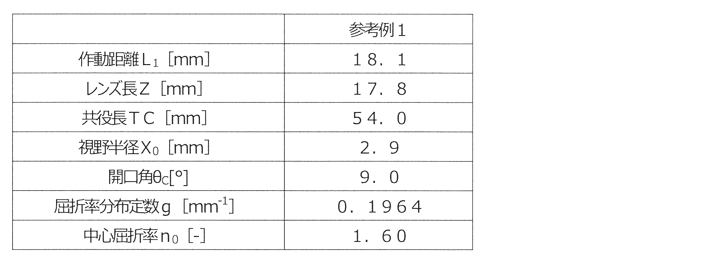
- Table 2 shows the working distance L 1 , lens length Z, conjugate length TC, field radius X 0 , aperture angle ⁇ C , refractive index distribution constant g [mm ⁇ 1 ], and refractive index n 0 at the central axis of the lens.
- a pair of rectangular FRP flat plates arranged parallel to each other were used to arrange the multiple lenses according to Reference Example 1 in two rows along the longitudinal direction of the flat plates at intervals of 1 mm so that they were parallel to each other.
- a black-colored adhesive resin was filled between the flat plates and cured to fix the multiple lenses.
- both ends of each lens were cut and both end faces were polished.
- Another pair of FRP substrates were arranged at both ends of the flat plates in the longitudinal direction, and the multiple lenses and the adhesive parts obtained by curing the adhesive resin were housed in a frame formed by these FRP flat plates. In this way, the lens array according to Reference Example 1 was obtained.
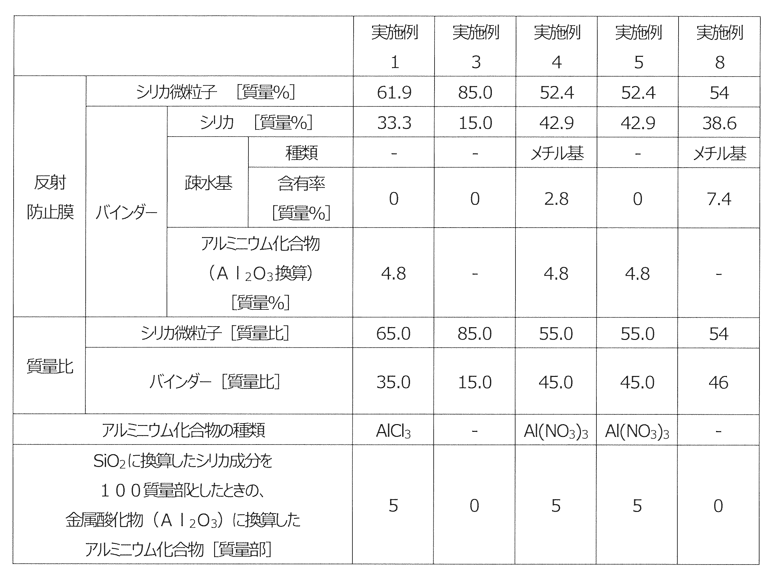
- Example 1 28.3 parts by mass of silica fine particle dispersion (Quatron PL-7, roughly spherical primary particles with an average particle size of 125 nm, solid content concentration of 23% by weight, manufactured by Fuso Chemical Co., Ltd.), 58.6 parts by mass of 1-methoxy-2-propanol (solvent), and 1 part by mass of 1N hydrochloric acid (hydrolysis catalyst) were mixed by stirring, and 12.1 parts by mass of tetraethoxysilane (ethyl orthosilicate, manufactured by Tama Chemical Co., Ltd.) was added while further stirring, and the mixture was stirred for 8 hours while keeping the temperature at 40°C to hydrolyze tetraethoxysilane, thereby obtaining stock solution A.
- stock solution A the ratio of the mass of silica fine particles to the mass of the hydrolysis condensation product of the hydrolyzable silicon compound contained in the binder was 65:35.
- the solid concentration of silica (derived from silica fine particles and alkoxysilane) converted to SiO2 was 1.6% by mass
- the aluminum compound converted to Al2O3 when the oxide of silicon converted to SiO2 was 100 parts by mass was 5.0 parts by mass.
- the coating liquid of Example 1 was applied by dip coating to both end faces in the lens length direction of a lens array produced in the same manner as in Reference Example 1 to form a coating film.
- the lens array was fixed to the support of a dip coater with a clip, immersed in the coating liquid of Example 1 that filled a container, and pulled up at a speed of 2.6 mm/sec to form a coating film.
- This coating film was heated at 200°C for 1800 seconds to form an anti-reflection film on both end faces in the lens length direction of the lens array. In this manner, the lens array of Example 1 was obtained.
- Example 2 A coating liquid according to Example 2 was obtained in the same manner as in Example 1, except that the aluminum chloride aqueous solution was not added.
- a lens array according to Example 2 was obtained in the same manner as in Example 1, except that the coating liquid according to Example 2 was used instead of the coating liquid according to Example 1.
- Example 3 A coating liquid according to Example 3 was prepared in the same manner as in Example 2, except that the amount of each raw material added was adjusted so that the content of each component was as shown in Table 3. The solid content concentration in the coating liquid according to Example 3 was 1.3 mass%.
- a lens array according to Example 3 was obtained in the same manner as in Example 1, except that the coating liquid according to Example 3 was used instead of the coating liquid according to Example 1, and the pulling speed in dip coating was adjusted to 2.0 mm/sec.
- Example 4 In addition to tetraethoxysilane, methyltriethoxysilane (manufactured by Shin-Etsu Chemical Co., Ltd.) was further added, and the amount of each raw material added was adjusted so that the content of each component was as shown in Table 3.
- the coating liquid according to Example 4 was prepared in the same manner as Example 1. Aluminum nitrate was used as the aluminum compound instead of aluminum chloride. The concentration of the solid content in the coating liquid according to Example 4 was 1.6 mass%. The content of the methyl group, which is a hydrophobic group, in the solid content of the coating liquid was 2.8 mass%.
- the lens array according to Example 4 was obtained in the same manner as Example 1, except that the coating liquid according to Example 4 was used instead of the coating liquid according to Example 1.
- Example 5 A coating liquid according to Example 5 was prepared in the same manner as in Example 4, except that methyltriethoxysilane was not added and the amount of each raw material added was adjusted so that the content of each component was as shown in Table 3.
- a lens array according to Example 5 was obtained in the same manner as in Example 1, except that the coating liquid according to Example 5 was used instead of the coating liquid according to Example 1.
- Example 6 A lens array according to Example 6 was obtained in the same manner as in Example 1, except for the following points. The amount of each component was adjusted so that the solid content concentration was 2.5 mass % to prepare a coating liquid according to Example 6. In dip coating, the coating liquid according to Example 6 was used instead of the coating liquid according to Example 1, and the pull-up speed in dip coating was adjusted to 1.0 mm/sec.
- Example 7 A lens array according to Example 7 was obtained in the same manner as in Example 1, except for the following points. The amount of each component was adjusted so that the solid content concentration was 3.5 mass % to prepare a coating liquid according to Example 7. In dip coating, the coating liquid according to Example 7 was used instead of the coating liquid according to Example 1, and the pull-up speed in dip coating was adjusted to 1.0 mm/sec.
- Example 8 0.6 g of tetraethoxysilane (TEOS) (manufactured by Tokyo Chemical Industry Co., Ltd.), 1.18 g of methyltriethoxysilane (MTES) (manufactured by Tokyo Chemical Industry Co., Ltd.), 0.82 g of 0.3 mass% formic acid (manufactured by Kishida Chemical Co., Ltd.), 3 g of hollow silica particle-containing sol (manufactured by JGC Catalysts and Chemicals, product name: Sururia 4110), and 22.4 g of ethanol (manufactured by Kishida Chemical Co., Ltd.) were mixed and reacted at 35 ° C. for 3 hours.
- TEOS tetraethoxysilane
- MTES methyltriethoxysilane
- Kishida Chemical Co., Ltd. 3 g
- hollow silica particle-containing sol manufactured by JGC Catalysts and Chemicals, product name: Sur
- the hollow silica particle-containing sol used contained a solvent and contained 25 mass% hollow silica as a solid content, and the average particle diameter of the hollow silica particles in the particle size distribution based on the number was about 50 nm.
- the thickness of the shell made of silica of the hollow silica particles was 10 to 20 nm.
- the maximum dimension of the internal space of the hollow silica particles was about 10 to 30 nm.
- the refractive index of the hollow particles was 1.25. In this way, a coating liquid according to Example 8 was obtained.
- the content of the solid content derived from TEOS was 0.6% by mass in terms of silica
- the content of methylsilsesquioxane (MeSq) which is a solid content derived from MTES was 1.6% by mass
- the content of hollow silica particles was 2.6% by mass.
- the silica derived from TEOS was 13%
- the MeSq derived from MTES was 33%
- the hollow silica particles were 54% by mass based on the mass.
- the content of the hollow silica particles was calculated on the assumption that the solid content of the hollow silica particle-containing sol was 25% by mass, and that the solid content was hollow silica particles.
- FIG. 6 is a cross-sectional view showing a schematic antireflection film in the lens array according to Example 8. 6 , the antireflection coating 20 is disposed in contact with an end face in the longitudinal direction of the lens 11.
- the antireflection coating 20 contains hollow silica particles 53 and a binder 54, and voids 55 exist inside the antireflection coating 20 and at the boundary between the antireflection coating 20 and the end face of the lens 11.
- the end face of the lens array was rubbed 40 times with Toray (registered trademark), a cloth manufactured by Toray Industries, Inc., and then the light quantity was evaluated in the same manner. The cloth was dried.
- Toray registered trademark
- the end face of the lens array was rubbed 40 times with a cloth soaked in ethanol, and then the light quantity was evaluated in the same manner. The results are shown in Table 4.
- the speed of moving the pencil was 1 mm/sec, and the distance of moving the pencil was adjusted to 20 mm or more.
- the pencil core powder attached to the anti-reflection film was wiped off with ethanol-soaked Bemcot, and the scratches on the anti-reflection film resulting from the test were observed under an optical microscope.
- the pencil hardness of the anti-reflective film was evaluated as the hardness that was one level softer than the hardness at which the anti-reflective film was scratched or peeled off to expose the substrate surface, in other words, the maximum hardness at which the anti-reflective film was not scratched or peeled off to expose the substrate surface. The results are shown in Table 4.
- the thickness T1 of the anti-reflection film was determined as the product of the arithmetic average D1 and the filling rate f. The results are shown in Table 4.
- the arithmetic average T2 of the thickness of the base at the site of the anti-reflection film used to obtain the arithmetic average D1 was obtained.
- the thickness T3 of the low refractive index portion was determined by subtracting the arithmetic mean T2 of the thickness of the base portion from the thickness T1 of the antireflection film.
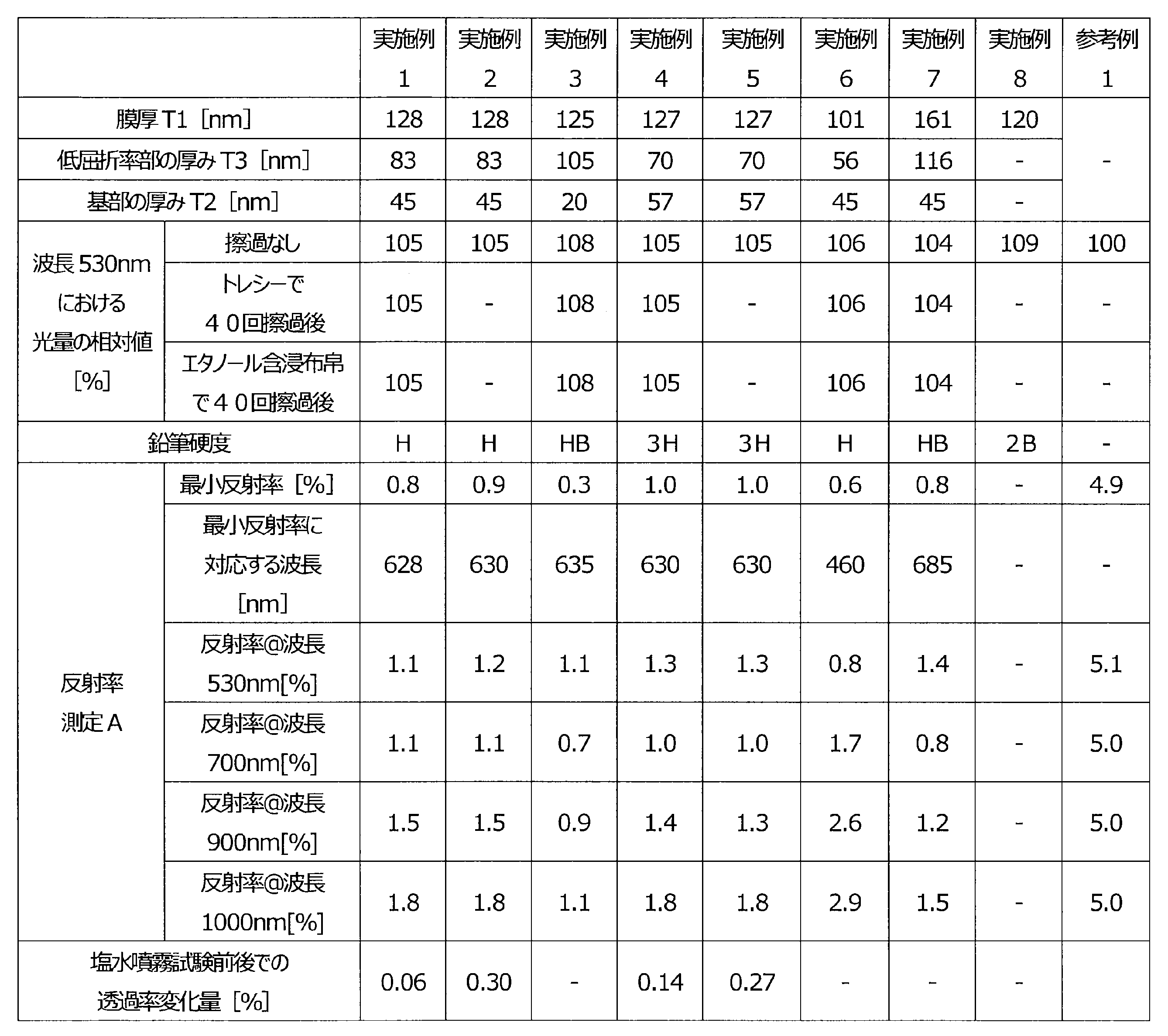
- Table 4 FE-SEM photographs of the cross sections of the antireflection films formed on the lens arrays according to Examples 1, 6, and 7 are shown in Figures 5A, 5B, and 5C, respectively.
- Reflectance Measurement A Using a near-infrared microspectrometer USPM-RU-W manufactured by Olympus Corporation, the reflectance of one end face in the lens length direction of the lens array of Reference Example 1 and Examples 1 to 7 was measured. In this measurement, the wavelength range was set to a range of 380 to 1050 nm, and the diameter of the measurement range was adjusted to 70 ⁇ m using an objective lens with a magnification of 10 times. In addition, the measurement position of the reflectance was adjusted to the center position of the lens of the lens array. The results are shown in Table 4.
- Reflectance Measurement B An anti-reflection film was formed on the surface of a glass plate in the same manner as in Examples 1 and 3, except that a float glass substrate was used instead of a lens array.
- an optical interference film which is a dielectric multilayer film, was formed on the surface of a float glass substrate by a physical vapor deposition (PVD) method, to obtain an anti-reflection film according to Comparative Example 1.
- PVD physical vapor deposition
- the reflectance of the surface of a glass plate on which an anti-reflection film was not formed was also measured in the same manner.
- the wavelength range was set to a range of 380 to 1050 nm, and the diameter of the measurement range was adjusted to 70 ⁇ m using an objective lens having a magnification of 10 times. The results are shown in Table 5.
- Salt spray test With reference to JIS C8917:2005, a salt spray test was carried out by spraying salt water on the end faces in the lens length direction of the lens arrays according to Examples 1 to 5.
- the environmental temperature of the lens array was adjusted to 35°C, and a 5% by mass aqueous solution of sodium chloride was used as the salt water.
- the salt spray was carried out for 96 hours.
- the amount of change in transmittance of the lens array before and after the salt spray test was measured. For this measurement, light with a wavelength in the range of 380 to 850 nm was used, and the amount of change in the average transmittance in this range was obtained. The results are shown in Table 5.
- the working distance L1 of the lenses of the lens array according to each embodiment is 5 mm or more, even when the lens array is used in an apparatus that inspects for defects by using reflected light from a transported inspection object, sufficient space can be secured for maintenance of the apparatus.
- the anti-reflection film can exhibit high anti-reflection performance and can increase the amount of light passing through the lens array.
- Example 4 suggests that the anti-reflective film exhibits a predetermined anti-reflective performance, has high pencil hardness, and is highly scratch-resistant.
- the anti-reflection films formed by the coating liquids of Examples 1 and 3 can reduce the reflectance at wavelengths of 530 nm, 700 nm, 900 nm, and 1000 nm, compared to a glass plate on which this anti-reflection film is not formed.
- these anti-reflection films can prevent the reflectance from increasing sharply with increasing wavelength, as seen in Comparative Example 1, and it can be understood that they can exhibit anti-reflection properties even at wavelengths in the near-infrared region.
- Example 1 As shown in Table 4, by comparing Example 1 and Example 2, the change in transmittance before and after the salt spray test is small in Example 1, and it is understood that the anti-reflection film of the lens array according to Example 1 has higher chemical resistance, especially higher alkali resistance, than the anti-reflection film of the lens array according to Example 2. It is understood that the inclusion of an aluminum compound in the binder of the anti-reflection film is advantageous from the viewpoint of enhancing chemical resistance, especially higher alkali resistance.
- Example 4 By comparing Example 4 and Example 5, the change in transmittance before and after the salt spray test is small in Example 4, and it is understood that the anti-reflection film of the lens array according to Example 4 has higher chemical resistance, especially higher alkali resistance, than the anti-reflection film of the lens array according to Example 5. It is understood that the inclusion of a hydrophobic group such as a methyl group in the binder of the anti-reflection film is advantageous from the viewpoint of enhancing chemical resistance, especially higher alkali resistance.
- the surface layer of the anti-reflection film formed on the lens array according to Examples 1, 6, and 7 had a low refractive index portion having unevenness formed by arranging silica fine particles to form a single layer or multiple layers.
- the refractive index of silica it is understood that the refractive index of the low refractive index portion is lower than the refractive index n 0 at the central axis of the lens of the lens array.
- a base was formed between the unevenness of this surface layer and the lens array, and the binder formed a phase in the base.
- the base of the anti-reflection film contains a large amount of binder, and it is considered that the binder content in the base is higher than the binder content in the low refractive index portion on a mass basis.
Landscapes
- Chemical & Material Sciences (AREA)
- Materials Engineering (AREA)
- Engineering & Computer Science (AREA)
- Chemical Kinetics & Catalysis (AREA)
- General Chemical & Material Sciences (AREA)
- Geochemistry & Mineralogy (AREA)
- Life Sciences & Earth Sciences (AREA)
- Organic Chemistry (AREA)
- Physics & Mathematics (AREA)
- General Physics & Mathematics (AREA)
- Optics & Photonics (AREA)
- Ceramic Engineering (AREA)
- Surface Treatment Of Optical Elements (AREA)
Abstract
Description
搬送されている被検査物からの反射光によって欠点の有無を検査する機器に用いられるレンズアレイであって、
前記被検査物の搬送方向である第一方向及び前記搬送方向に垂直な第二方向に配列され、前記反射光を集光させる複数のレンズと、
前記レンズ同士を固定する接着部と、
前記複数のレンズ及び前記接着部を収容する筐体と、
反射防止膜と、を備え、
前記反射防止膜は、前記レンズの屈折率以下の屈折率を有する微粒子と、バインダーとを含み、前記反射光が入射する前記レンズの第一面及び前記第一面に入射した光が出射される前記レンズの第二面からなる群より選ばれる少なくとも1つに接して配置されており、
前記バインダーは、前記微粒子を前記第一面又は前記第二面に接着させている、
レンズアレイを提供する。
n(r)2=n0 2{1-(g・r)2} 式(1)
モル%で示して、
40%≦SiO2≦65%
0%≦TiO2≦10%
0.1%≦MgO≦22%
0.15%≦ZnO≦15%
0.5%≦Li2O≦15%
2%≦Na2O≦20%
0%≦B2O3≦20%
0%≦Al2O3≦10%
0%≦K2O≦3%
0%≦Cs2O≦3%
0%≦Y2O3≦5%
0%≦ZrO2≦2%
0%≦Nb2O5≦5%
0%≦In2O3≦5%
0%≦La2O3≦5%
0%≦Ta2O5≦5%、を含む組成。
(I)上記の組成を有するガラス素線を作製する。
(II)上記の組成に含まれる第一アルカリ金属元素Qとは異なる第二アルカリ金属元素Rを含む溶融塩にガラス素線を浸漬して、ガラス素線中の第一アルカリ金属元素Qと溶融塩中の第二アルカリ金属元素Rとをイオン交換処理することにより、ガラス素線に屈折率分布を形成する。
SiX4 (Ia)
RSiY3 (IIa)
表1に示す組成となるようにガラス原料を混合し、混合物を熔融して、参考例1に係る熔融ガラス(ガラス組成物)を得た。表1における数値はモル%を示す。参考例1に係る熔融ガラスを紡糸してファイバー状に成形し、得られたガラスファイバーを所定の長さで切断し、切断面を研磨した。これにより、参考例1に係るガラス素線を得た。ガラス素線の直径(線径)は、1000μmであった。次に、各ガラス素線を構成するガラス組成物のガラス転移温度付近に加熱した硝酸ナトリウム溶融塩に各ガラス素線を浸漬し、イオン交換処理を行った。これにより、各ガラス素線に屈折率分布を形成した。その後、イオン交換処理後のガラス素線を所定の長さに切断し、参考例1に係るレンズを得た。表2にこのレンズの作動距離L1、レンズ長Z、共役長TC、視野半径X0、開口角θC、屈折率分布定数g[mm-1]、レンズの中心軸線における屈折率n0を示す。
シリカ微粒子分散液(クォートロンPL-7、平均粒径125nmの略球状の一次粒子、固形分濃度23重量%、扶桑化学工業株式会社製)28.3質量部、1‐メトキシ‐2‐プロパノール(溶媒)58.6質量部、1N塩酸(加水分解触媒)1質量部を撹拌混合し、さらに撹拌しながらテトラエトキシシラン(正珪酸エチル、多摩化学工業株式会社製)12.1質量部を添加し、引き続き40℃に保温しながら8時間撹拌してテトラエトキシシランを加水分解し、原液Aを得た。原液Aにおいて、シリカ微粒子の質量と、バインダーに含まれる加水分解性シリコン化合物の加水分解縮合生成物の質量との比は、65:35であった。
塩化アルミニウム水溶液を添加しなかったこと以外は実施例1と同様にして、実施例2に係るコーティング液を得た。実施例1に係るコーティング液の代わりに実施例2に係るコーティング液を用いたこと以外は実施例1と同様にして、実施例2に係るレンズアレイを得た。
各成分の含有率が表3に示す通りになるように各原料の添加量を調整した以外は、実施例2と同様にして実施例3に係るコーティング液を調製した。なお、実施例3に係るコーティング液における固形分の濃度は1.3質量%であった。実施例1に係るコーティング液の代わりに実施例3に係るコーティング液を用い、かつ、ディップコーティングにおける引き上げ速度を2.0mm/秒に調節したこと以外は、実施例1と同様にして、実施例3に係るレンズアレイを得た。
テトラエトキシシランに加えて、メチルトリエトキシシラン(信越化学工業株式会社製)をさらに添加し、かつ、各成分の含有率が表3に示す通りになるように各原料の添加量を調整したこと以外は、実施例1と同様にして実施例4に係るコーティング液を調製した。アルミニウム化合物としては、塩化アルミニウムの代わりに硝酸アルミニウムを用いた。なお、実施例4に係るコーティング液における固形分の濃度は1.6質量%であった。コーティング液の固形分において、疎水基であるメチル基の含有率は、2.8質量%であった。実施例1に係るコーティング液の代わりに実施例4に係るコーティング液を用いたこと以外は、実施例1と同様にして、実施例4に係るレンズアレイを得た。
メチルトリエトキシシランを添加せずに、各成分の含有率が表3に示す通りになるように各原料の添加量を調整したこと以外は、実施例4と同様にして実施例5に係るコーティング液を調製した。実施例1に係るコーティング液の代わりに実施例5に係るコーティング液を用いたこと以外は、実施例1と同様にして、実施例5に係るレンズアレイを得た。
下記の点以外は、実施例1と同様にして、実施例6に係るレンズアレイを得た。固形分濃度が2.5質量%となるように各成分の量を調節して実施例6に係るコーティング液を調製した。ディップコーティングにおいて、実施例1に係るコーティング液の代わりに実施例6に係るコーティング液を用い、ディップコーティングにおける引き上げ速度を1.0mm/秒に調節した。
下記の点以外は、実施例1と同様にして、実施例7に係るレンズアレイを得た。固形分濃度が3.5質量%となるように各成分の量を調節して実施例7に係るコーティング液を調製した。ディップコーティングにおいて、実施例1に係るコーティング液の代わりに実施例7に係るコーティング液を用い、ディップコーティングにおける引き上げ速度を1.0mm/秒に調節した。
テトラエトキシシラン(TEOS)(東京化成工業社製)0.6g、メチルトリエトキシシラン(MTES)(東京化成工業社製)1.18g、0.3質量%のギ酸(キシダ化学社製)0.82g、中空シリカ粒子含有ゾル(日揮触媒化成社製、製品名:スルーリア4110)3g、及びエタノール(キシダ化学社製)22.4gを混ぜ、35℃で3時間反応させた。用いた中空シリカ粒子含有ゾルは、溶剤を含み、固形分として25質量%の中空シリカを含有するものであり、個数基準の粒度分布における中空シリカ粒子の平均粒子径は約50nmであった。中空シリカ粒子のシリカでできたシェルの厚みは10~20nmであった。中空シリカ粒子の内部空間の最大寸法は約10~30nmであった。中空粒子の屈折率は、1.25であった。このようにして、実施例8に係るコーティング液を得た。実施例8に係るコーティング液において、TEOSに由来する固形分の含有量は、シリカに換算して0.6質量%であり、MTESに由来する固形分であるメチルシルセスキオキサン(MeSq)の含有量が1.6質量%であり、中空シリカ粒子の含有量が2.6質量%であった。実施例8に係るコーティング液の固形分において、質量基準で、TEOS由来のシリカが13%、MTESに由来するMeSqが33%、中空シリカ粒子が54%含まれていた。なお、中空シリカ粒子の含有量は、中空シリカ粒子含有ゾルのうち固形分が25質量%であり、その固形分が中空シリカ粒子であると仮定したうえで求めた。また、実施例8に係るコーティング液の調製において加えられたTEOSの物質量に対するMTESの物質量の比は、7/3であった。実施例2に係るコーティング液の代わりに実施例8に係るコーティング液を用いたこと以外は、実施例2と同様にして、実施例8に係るレンズアレイを得た。図6は、実施例8に係るレンズアレイにおける反射防止膜を模式的に示す断面図である。図6に示す通り、反射防止膜20は、レンズ11の長さ方向における端面に接して配置されている。反射防止膜20は、中空シリカ粒子53と、バインダー54とを含み、反射防止膜20の内部及び反射防止膜20とレンズ11の端面との境界にはボイド55が存在していた。
各実施例のレンズアレイのレンズの作動距離に対応する物体面に平坦な反射板を配置し、光源からの光を反射させて生じた反射光をレンズアレイに入射させ、レンズアレイの像面に対応する位置における光量[lx]を測定した。波長530nmにおける参考例1のレンズアレイを用いた場合の光量を100とした場合の、波長530nmにおける実施例1~7のレンズアレイを用いた場合の光量の相対値を求めた。結果を表4に示す。実施例1、3、4、6、及び7に係るレンズアレイについて、東レ社製のクロスであるトレシー(登録商標)でレンズアレイの端面を40回擦った後に、光量を同様にして評価した。クロスは乾燥させたものを用いた。実施例1、3、4、6、及び7に係るレンズアレイについて、エタノールをしみこませた布帛でレンズアレイの端面を40回擦った後に、光量を同様にして評価した。結果を表4に示す。
鉛筆硬度試験機(Pencil Scratch Hardness Tester Model: 720N, Brand: Sheen Instruments - UK)及び鉛筆(UNI、三菱鉛筆、硬度2B~9H)を用いて、日本産業規格(JIS)K 5600-5-4に準拠して、実施例1~8に係るレンズアレイに形成された反射防止膜に対して、鉛筆硬度試験を実施した。この試験において、鉛筆の反射防止膜に対する角度は45°であり、鉛筆は荷重750gで押された状態であった。いくつかの水準の硬度を有する鉛筆の芯を、次第に硬度を増しながら反射防止膜に押し付けて動かすことによって鉛筆硬度を測定した。この測定において、鉛筆を動かす速度は1mm/秒であり、鉛筆を動かす距離は20mm以上に調整された。試験後に、反射防止膜に付着した鉛筆芯の粉をエタノールが染み込んだベンコットでふき取り、反射防止膜において試験の結果生じた傷跡を光学顕微鏡で観察した。反射防止膜が取れたひっかき傷が発生する、又は、基板面が露出するように反射防止膜の剥離が起こったときの硬度よりも一段階軟らかい硬度、換言すると、反射防止膜に傷が発生しなかった最大硬度又は基板面が露出する剥離が発生しなかった最大硬度を、反射防止膜の鉛筆硬度として評価した。結果を表4に示す。
電界放射型走査型電子顕微鏡(FE-SEM)(日立製作所社製、型式:S‐4500)を用いて、実施例1~7に係るレンズアレイに形成された反射防止膜の断面を観察した。反射防止膜の10°斜め上方からの断面におけるFE-SEM写真において、シリカ微粒子の平均粒径の10倍に相当する距離(1250nm)の部位に現れる反射防止膜の表層の凹凸の各凸部の最外部と、反射防止膜に接するレンズアレイの端面との間の反射防止膜の厚み方向における距離を測定し、その距離の算術平均D1を求めた。さらに、その部位に現れる凸部の数を特定した。その数を10で除して単位距離におけるシリカ微粒子の充填率fを特定した。反射防止膜の厚みT1を算術平均D1と充填率fとの積として決定した。結果を表4に示す。加えて、算術平均D1を求めるために用いられた反射防止膜の部位における基部の厚みの算術平均T2を求めた。反射防止膜の厚みT1から基部の厚みの算術平均T2を差し引いて低屈折率部の厚みT3を決定した。結果を表4に示す。実施例1、6、及び7に係るレンズアレイに形成された反射防止膜の断面のFE-SEM写真を、それぞれ、図5A、図5B、及び図5Cに示す。
オリンパス社製の近赤外顕微分光測定機USPM-RU-Wを用いて、参考例1及び実施例1~7に係るレンズアレイのレンズアレイのレンズ長さ方向における一方の端面の反射率を測定した。この測定では、波長範囲を380~1050nmの範囲に設定し、10倍の倍率を有する対物レンズを用いて測定範囲の直径を70μmに調整した。加えて、反射率の測定位置は、レンズアレイのレンズの中心位置に調整した。結果を表4に示す。
レンズアレイの代わりにフロートガラス基板を用いたこと以外は実施例1及び3と同様にして、ガラス板の表面に反射防止膜を形成した。加えて、フロートガラス基板の表面に物理蒸着(PVD)法によって誘電体多層膜である光学干渉膜を形成し、比較例1に係る反射防止膜を得た。オリンパス社製の近赤外顕微分光測定機USPM-RU-Wを用いて、ガラス板の表面に形成されたこれらの反射防止膜の反射率を測定した。加えて、反射防止膜が形成されていないガラス板の表面の反射率も同様に測定した。この測定では、波長範囲を380~1050nmの範囲に設定し、倍率10倍の倍率を有する対物レンズを用いて測定範囲の直径を70μmに調整した。結果を表5に示す。
JIS C8917:2005を参考に、実施例1~5に係るレンズアレイのレンズ長さ方向における端面に塩水を噴霧する塩水噴霧試験を実施した。この塩水噴霧試験において、レンズアレイの環境温度は35℃に調節し、塩水として5質量%の塩化ナトリウム水溶液を用いた。加えて、塩水噴霧を96時間行った。塩水噴霧試験前後におけるレンズアレイの透過率変化量を測定した。この測定には、波長380~850nmの範囲の光を用い、この範囲における透過率の平均値の変化量を求めた。結果を表5に示す。


Claims (17)
- 搬送されている被検査物からの反射光によって欠点の有無を検査する機器に用いられるレンズアレイであって、
前記被検査物の搬送方向である第一方向及び前記搬送方向に垂直な第二方向に配列され、前記反射光を集光させる複数のレンズと、
前記レンズ同士を固定する接着部と、
前記複数のレンズ及び前記接着部を収容している筐体と、
反射防止膜と、を備え、
前記反射防止膜は、前記レンズの屈折率以下の屈折率を有する微粒子と、バインダーとを含み、前記反射光が入射する前記レンズの第一面及び前記第一面に入射した光が出射される前記レンズの第二面からなる群より選ばれる少なくとも1つに接して配置されており、
前記バインダーは、前記微粒子を前記第一面又は前記第二面に接着させている、
レンズアレイ。 - 前記レンズは、屈折率分布型レンズである、
請求項1に記載のレンズアレイ。 - 前記反射防止膜は、前記微粒子によって形成された凹凸を含む表層を有する、
請求項1又は2に記載のレンズアレイ。 - 前記反射防止膜は、前記反射防止膜の厚み方向における前記凹凸と前記レンズとの間に基部を含み、
前記バインダーは、前記基部において前記微粒子同士の間で層をなしている、
請求項3に記載のレンズアレイ。 - 前記反射防止膜と前記レンズとの間には、シリコン原子が関与する結合が形成されている、
請求項1~4のいずれか1項に記載のレンズアレイ。 - 前記微粒子は、シリカを主成分として含む、
請求項1~5のいずれか1項に記載のレンズアレイ。 - 前記微粒子と前記バインダーとの間には、シリコン原子が関与する結合が形成されている、
請求項6に記載のレンズアレイ。 - 前記微粒子は、80~600nmの平均粒径を有する、
請求項1~7のいずれか1項に記載のレンズアレイ。 - 前記反射防止膜は、80~800nmの膜厚を有する、
請求項1~8のいずれか1項に記載のレンズアレイ。 - 前記反射防止膜における前記バインダーの含有率は、5~64質量%であり、
前記反射防止膜における前記微粒子の含有率は、35~90質量%である、
請求項1~9のいずれか1項に記載のレンズアレイ。 - 前記バインダーは、疎水基を含んでいる、
請求項1~10のいずれか1項に記載のレンズアレイ。 - 前記バインダーにおける前記疎水基の含有率は、10質量%以下である。
請求項11に記載のレンズアレイ。 - 前記バインダーは、アルミニウム化合物を含んでいる、
請求項1~12のいずれか1項に記載のレンズアレイ。 - 前記反射防止膜における前記アルミニウム化合物の含有率は、前記アルミニウム化合物をAl2O3に換算して7質量%以下である、
請求項13に記載のレンズアレイ。 - 前記レンズは、15mm以上の作動距離を有する、
請求項1~14のいずれか1項に記載のレンズアレイ。 - 前記レンズは、モル%で示して、
40%≦SiO2≦65%
0%≦TiO2≦10%
0.1%≦MgO≦22%
0.15%≦ZnO≦15%
0.5%≦Li2O≦15%
2%≦Na2O≦20%
0%≦B2O3≦20%
0%≦Al2O3≦10%
0%≦K2O≦3%
0%≦Cs2O≦3%
0%≦Y2O3≦5%
0%≦ZrO2≦2%
0%≦Nb2O5≦5%
0%≦In2O3≦5%
0%≦La2O3≦5%
0%≦Ta2O5≦5%、を含む中心部を有する、
請求項1~15のいずれか1項に記載のレンズアレイ。 - 前記複数のレンズは、前記第二方向に複数の列をなしている、
請求項1~16のいずれか1項に記載のレンズアレイ。
Priority Applications (3)
| Application Number | Priority Date | Filing Date | Title |
|---|---|---|---|
| KR1020257014696A KR20250073491A (ko) | 2022-10-31 | 2023-10-27 | 렌즈 어레이 |
| JP2024554481A JPWO2024095931A1 (ja) | 2022-10-31 | 2023-10-27 | |
| CN202380070249.7A CN119998694A (zh) | 2022-10-31 | 2023-10-27 | 透镜阵列 |
Applications Claiming Priority (2)
| Application Number | Priority Date | Filing Date | Title |
|---|---|---|---|
| JP2022174058 | 2022-10-31 | ||
| JP2022-174058 | 2022-10-31 |
Publications (1)
| Publication Number | Publication Date |
|---|---|
| WO2024095931A1 true WO2024095931A1 (ja) | 2024-05-10 |
Family
ID=90930494
Family Applications (1)
| Application Number | Title | Priority Date | Filing Date |
|---|---|---|---|
| PCT/JP2023/038981 Ceased WO2024095931A1 (ja) | 2022-10-31 | 2023-10-27 | レンズアレイ |
Country Status (4)
| Country | Link |
|---|---|
| JP (1) | JPWO2024095931A1 (ja) |
| KR (1) | KR20250073491A (ja) |
| CN (1) | CN119998694A (ja) |
| WO (1) | WO2024095931A1 (ja) |
Citations (4)
| Publication number | Priority date | Publication date | Assignee | Title |
|---|---|---|---|---|
| JPH11292568A (ja) * | 1997-12-09 | 1999-10-26 | Nippon Sheet Glass Co Ltd | 反射防止ガラス板、その製造方法および反射防止膜用被覆組成物 |
| US20200189951A1 (en) * | 2017-04-24 | 2020-06-18 | Lg Electronics Inc. | Curved glass and manufacturing method thereof |
| WO2021171912A1 (ja) * | 2020-02-28 | 2021-09-02 | 日本板硝子株式会社 | 低屈折率膜、積層体、光学素子、防風材、及び表示装置 |
| WO2021261319A1 (ja) * | 2020-06-25 | 2021-12-30 | 日本板硝子株式会社 | ロッドレンズアレイ、光学機器、イメージセンサ、プリンタ、検査装置、屈折率分布型ロッドレンズ用母材ガラス組成物、及び屈折率分布型ロッドレンズの製造方法 |
Family Cites Families (2)
| Publication number | Priority date | Publication date | Assignee | Title |
|---|---|---|---|---|
| WO2014192933A1 (ja) | 2013-05-31 | 2014-12-04 | コニカミノルタ株式会社 | 積層型レンズアレイユニット及び撮像装置 |
| US11300785B2 (en) * | 2018-07-11 | 2022-04-12 | Denso International America, Inc. | Head-up display (HUD) mirror assembly and housing |
-
2023
- 2023-10-27 CN CN202380070249.7A patent/CN119998694A/zh active Pending
- 2023-10-27 KR KR1020257014696A patent/KR20250073491A/ko active Pending
- 2023-10-27 JP JP2024554481A patent/JPWO2024095931A1/ja active Pending
- 2023-10-27 WO PCT/JP2023/038981 patent/WO2024095931A1/ja not_active Ceased
Patent Citations (4)
| Publication number | Priority date | Publication date | Assignee | Title |
|---|---|---|---|---|
| JPH11292568A (ja) * | 1997-12-09 | 1999-10-26 | Nippon Sheet Glass Co Ltd | 反射防止ガラス板、その製造方法および反射防止膜用被覆組成物 |
| US20200189951A1 (en) * | 2017-04-24 | 2020-06-18 | Lg Electronics Inc. | Curved glass and manufacturing method thereof |
| WO2021171912A1 (ja) * | 2020-02-28 | 2021-09-02 | 日本板硝子株式会社 | 低屈折率膜、積層体、光学素子、防風材、及び表示装置 |
| WO2021261319A1 (ja) * | 2020-06-25 | 2021-12-30 | 日本板硝子株式会社 | ロッドレンズアレイ、光学機器、イメージセンサ、プリンタ、検査装置、屈折率分布型ロッドレンズ用母材ガラス組成物、及び屈折率分布型ロッドレンズの製造方法 |
Also Published As
| Publication number | Publication date |
|---|---|
| JPWO2024095931A1 (ja) | 2024-05-10 |
| CN119998694A (zh) | 2025-05-13 |
| KR20250073491A (ko) | 2025-05-27 |
Similar Documents
| Publication | Publication Date | Title |
|---|---|---|
| CN110824666B (zh) | 胶合透镜、光学系统、光学装置和制造胶合透镜的方法 | |
| JP7118615B2 (ja) | 光学素子、光学系および撮像装置 | |
| TWI701456B (zh) | 低反射塗層、玻璃板、玻璃基板、及光電轉換裝置 | |
| WO2019021665A1 (ja) | 光学フィルタ | |
| JP2020079935A (ja) | 光吸収層及び光吸収層を製造する方法 | |
| JP6686222B2 (ja) | 光学フィルタ用組成物及び光学フィルタを製造する方法 | |
| JP2021185427A (ja) | 光学部材及び光学部材の製造方法 | |
| KR102623827B1 (ko) | 광학 필터 및 촬상 장치 | |
| CN119301080A (zh) | 低反射构件和低反射膜用涂敷液 | |
| JP2024023502A (ja) | 光吸収性組成物、光吸収膜、及び光学フィルタ | |
| US12071542B2 (en) | Light-absorbing composition and optical filter | |
| EP4266089B1 (en) | Article including porous layer containing inorganic particles, and coating liquid for forming porous layer containing inorganic particles | |
| JP7629395B2 (ja) | 光吸収性組成物及び光学フィルタ | |
| JP6543746B1 (ja) | 光学フィルタの製造方法 | |
| CN114249542B (zh) | 具有多孔层的部件和用于形成多孔层的涂覆液 | |
| JP2016018156A (ja) | 近赤外線吸収構造体、および、その製造方法 | |
| KR20250073491A (ko) | 렌즈 어레이 | |
| US20260023198A1 (en) | Light-absorbing composition, light absorber, optical filter, ambient light sensor, imaging apparatus, light-absorbing composition manufacturing method, and light absorber manufacturing method | |
| JP7343750B2 (ja) | 反射防止膜及びその製造方法、及びそれを用いた光学部材 | |
| JP7322107B2 (ja) | 多孔質層を有する部材および多孔質層を形成するための塗工液 | |
| JP7401351B2 (ja) | 部材、光学機器、塗工液、部材の製造方法、多孔質膜 | |
| JP7652793B2 (ja) | 光学フィルタ、撮像装置用光学フィルタ、撮像装置、及び撮像装置用光学フィルタの製造方法 | |
| WO2024095915A1 (ja) | レンズ集合体 | |
| JP2020194066A (ja) | 光学素子およびその製造方法、並びに光学素子を含む光学装置 | |
| JP4823569B2 (ja) | 光学ガラス部品及びその製造方法 |
Legal Events
| Date | Code | Title | Description |
|---|---|---|---|
| 121 | Ep: the epo has been informed by wipo that ep was designated in this application |
Ref document number: 23885687 Country of ref document: EP Kind code of ref document: A1 |
|
| WWE | Wipo information: entry into national phase |
Ref document number: 202380070249.7 Country of ref document: CN |
|
| WWE | Wipo information: entry into national phase |
Ref document number: 2024554481 Country of ref document: JP |
|
| ENP | Entry into the national phase |
Ref document number: 20257014696 Country of ref document: KR Kind code of ref document: A |
|
| WWP | Wipo information: published in national office |
Ref document number: 202380070249.7 Country of ref document: CN |
|
| NENP | Non-entry into the national phase |
Ref country code: DE |
|
| 122 | Ep: pct application non-entry in european phase |
Ref document number: 23885687 Country of ref document: EP Kind code of ref document: A1 |