WO2024090366A1 - 撮像装置 - Google Patents
撮像装置 Download PDFInfo
- Publication number
- WO2024090366A1 WO2024090366A1 PCT/JP2023/038133 JP2023038133W WO2024090366A1 WO 2024090366 A1 WO2024090366 A1 WO 2024090366A1 JP 2023038133 W JP2023038133 W JP 2023038133W WO 2024090366 A1 WO2024090366 A1 WO 2024090366A1
- Authority
- WO
- WIPO (PCT)
- Prior art keywords
- pixel
- dark current
- signal
- gain
- optical black
- Prior art date
- Legal status (The legal status is an assumption and is not a legal conclusion. Google has not performed a legal analysis and makes no representation as to the accuracy of the status listed.)
- Ceased
Links
Images







Classifications
-
- H—ELECTRICITY
- H04—ELECTRIC COMMUNICATION TECHNIQUE
- H04N—PICTORIAL COMMUNICATION, e.g. TELEVISION
- H04N25/00—Circuitry of solid-state image sensors [SSIS]; Control thereof
- H04N25/50—Control of the SSIS exposure
- H04N25/57—Control of the dynamic range
- H04N25/58—Control of the dynamic range involving two or more exposures
- H04N25/581—Control of the dynamic range involving two or more exposures acquired simultaneously
-
- H—ELECTRICITY
- H04—ELECTRIC COMMUNICATION TECHNIQUE
- H04N—PICTORIAL COMMUNICATION, e.g. TELEVISION
- H04N25/00—Circuitry of solid-state image sensors [SSIS]; Control thereof
- H04N25/60—Noise processing, e.g. detecting, correcting, reducing or removing noise
- H04N25/63—Noise processing, e.g. detecting, correcting, reducing or removing noise applied to dark current
Definitions
- the present invention relates to an imaging device that captures images, and in particular to an imaging device that captures images using a selective HDR (High Dynamic Range) method.
- HDR High Dynamic Range
- imaging devices that capture images using a selective HDR method are known.
- the present disclosure therefore aims to provide an imaging device capable of capturing high-quality images.
- An imaging device has a pixel section having: effective area pixels which are pixels that receive light and generate charges according to the amount of light received, and output N (N is an integer of 2 or more) pixel signals with different gains according to the amount of charge generated by the generated charges and the amount of charge generated by the dark current component; and N x M (M is an integer of 2 or more) optical black pixels which are pixels that do not receive light and output dark current pixel signals according to the amount of charge generated by the dark current component; a selection circuit which selects one of the N pixel signals based on at least one pixel signal of the N pixel signals, outputs the selected selected pixel signal, and generates and outputs a gain signal which specifies one of the M gains; and an A/D conversion circuit which converts the selected pixel signal based on the gain specified by the gain signal.
- the AD conversion circuit outputs a digital pixel signal, and further performs AD conversion on each of the N ⁇ M dark current pixel signals output from the N ⁇ M optical black pixels based on a fixed gain to the optical black pixel that output the dark current pixel signal, and outputs the AD-converted N ⁇ M dark current digital pixel signals; and a dark current calculation circuit calculates N ⁇ M dark current component signals in each of the N ⁇ M optical black pixels based on the N ⁇ M dark current digital pixel signals, and feeds them back to at least one of the selection circuit and the AD conversion circuit, and the N ⁇ M optical black pixels are configured to include M N optical black pixels each outputting a dark current pixel signal with a gain corresponding to each of the N pixel signals.
- the imaging device can capture high-quality images.
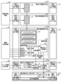
- FIG. 1 is a schematic diagram showing a configuration of an imaging device according to an embodiment.
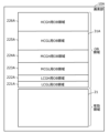
- FIG. 2 is a schematic diagram showing an example of an arrangement of effective area pixels and optical black pixels in a pixel section according to the embodiment.
- FIG. 3 is a schematic diagram showing configurations of a selection unit according to an embodiment, an AD conversion unit according to an embodiment, and a readout unit according to an embodiment.
- FIG. 4 is a schematic diagram for explaining main operations performed by each of the main components of the imaging device according to the embodiment.
- FIG. 5 is a schematic diagram showing how the AD conversion circuit according to the embodiment performs AD conversion on a selected pixel signal.
- FIG. 6 is a schematic diagram showing an example of how an HDR processing circuit according to a comparative example adjusts a gain ratio.
- FIG. 1 is a schematic diagram showing a configuration of an imaging device according to an embodiment.
- FIG. 2 is a schematic diagram showing an example of an arrangement of effective area pixels and optical black pixels in a pixel section according to the embodiment.
- FIG. 7 is a schematic diagram showing an example of how the HDR processing circuit according to the embodiment adjusts the gain ratio.
- FIG. 8 is a schematic diagram showing how the black levels are adjusted to match between a digital pixel signal obtained by performing AD conversion using a ramp signal H and a digital pixel signal obtained by performing AD conversion using a ramp signal L.
- FIG. 9 is a schematic diagram showing how the threshold generating circuit according to the embodiment calculates the threshold.
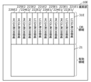
- FIG. 10 is a schematic diagram showing an example of an arrangement of effective area pixels and optical black pixels in a pixel section according to a modified example.
- FIG. 11 is a schematic diagram showing an example of an arrangement of effective area pixels and optical black pixels in a pixel section according to a modified example.
- FIG. 10 is a schematic diagram showing an example of an arrangement of effective area pixels and optical black pixels in a pixel section according to a modified example.
- FIG. 12 is a schematic diagram showing an example of an arrangement of effective area pixels and optical black pixels in a pixel section according to a modified example.
- FIG. 13 is a schematic diagram showing an example of an arrangement of effective area pixels and optical black pixels in a pixel section according to a modified example.
- FIG. 14 is a schematic diagram showing an example of an arrangement of effective area pixels and optical black pixels in a pixel section according to a modified example.
- FIG. 15 is a schematic diagram showing an example of an arrangement of effective area pixels and optical black pixels in a pixel section according to a modified example.
- the inventors have been developing an imaging device that captures an image using a selective HDR system. Through this development, the inventors have found that when pixels that output a plurality of pixel signals with different gains are used in an imaging device that captures an image using a selective HDR system, the following two inhibiting factors exist as factors that inhibit the improvement of image quality of the captured image.
- Inhibitory factor 1 The charge accumulated by a pixel includes charge generated according to the amount of received light and charge generated by dark current components. Therefore, when a pixel outputs a first pixel signal and a second pixel signal with different gains according to the amount of charge, if the amount of charge indicated by the first pixel signal and the amount of charge indicated by the second pixel signal are simply adjusted in proportion to the gain ratio when AD conversion is performed on the first pixel signal and the second pixel signal, the amount of charge generated by the dark current component will also be adjusted in proportion to the gain ratio. Therefore, it is not possible to maintain the linearity of the amount of charge generated according to the amount of received light between the first pixel signal and the second pixel signal in the digital signal after AD conversion. As a result, a brightness step occurs in the digital signal after AD conversion at the switching point where the pixel signal used for AD conversion is switched from the first pixel signal to the second pixel signal.
- Inhibitory factor 2 In order to improve the quality of an image to be captured, when a pixel outputs a first pixel signal and a second pixel signal, each of which has a different gain according to the amount of charge, it is desirable to use the pixel signal with the better S/N ratio for A/D conversion. Conventionally, the switching point for switching the pixel signal used for A/D conversion from the first pixel signal to the second pixel signal has been determined based on a pixel signal that includes a dark current component.
- the switching of the pixel signal used for A/D conversion from the first pixel signal to the second pixel signal is quicker by the amount of the dark current component included in the pixel signal.
- the switching of the pixel signal used for A/D conversion cannot be performed appropriately from the viewpoint of using the pixel signal with the better S/N ratio for A/D conversion.
- the inventors further conducted experiments and studies based on the idea that if at least one of these impediments 1 and 2 could be overcome, an imaging device capable of capturing high-quality images could be realized. As a result, the inventors came up with the imaging device according to one aspect of the present disclosure described below.
- An imaging device has a pixel section having: effective area pixels which are pixels that receive light and generate charges according to the amount of light received, and output N (N is an integer of 2 or more) pixel signals with different gains according to the amount of charge generated by the generated charges and the amount of charge generated by the dark current component; and N x M (M is an integer of 2 or more) optical black pixels which are pixels that do not receive light and output dark current pixel signals according to the amount of charge generated by the dark current component; a selection circuit which selects one of the N pixel signals based on at least one pixel signal of the N pixel signals, outputs the selected selected pixel signal, and generates and outputs a gain signal which specifies one of the M gains; and an A/D conversion circuit which converts the selected pixel signal based on the gain specified by the gain signal.
- the AD conversion circuit outputs a digital pixel signal, and further performs AD conversion on each of the N ⁇ M dark current pixel signals output from the N ⁇ M optical black pixels based on a fixed gain to the optical black pixel that output the dark current pixel signal, and outputs the AD-converted N ⁇ M dark current digital pixel signals; and a dark current calculation circuit calculates N ⁇ M dark current component signals in each of the N ⁇ M optical black pixels based on the N ⁇ M dark current digital pixel signals, and feeds them back to at least one of the selection circuit and the AD conversion circuit, and the N ⁇ M optical black pixels are configured to include M N optical black pixels each outputting a dark current pixel signal with a gain corresponding to each of the N pixel signals.
- N x M optical black pixels corresponding to each combination of N pixel signals and M gains are used to calculate N x M dark current component signals corresponding to each of these combinations.
- the calculated N x M dark current component signals are then fed back to at least one of the AD conversion circuit and the selection circuit.
- the AD conversion circuit uses the fed-back N x M dark current component signals to perform AD conversion so as to suppress the brightness step, thereby overcoming the above-mentioned inhibiting factor 1, i.e., it becomes possible to perform AD conversion so as to suppress the above-mentioned brightness step, and/or the selection circuit uses the fed-back N x M dark current component signals to select one of the N pixel signals so that the full range of the AD conversion circuit can be used only for AD conversion of the charge amount generated according to the amount of light received from among the charges accumulated by the pixel, and generates and outputs a gain signal that specifies one of the M gains, thereby overcoming the above-mentioned inhibiting factor 2, i.e., it becomes possible to appropriately switch the pixel signal used for AD conversion from the perspective of using the pixel signal with the better S/N ratio for AD conversion.
- the imaging device configured as described above provides an imaging device capable of capturing high-quality images.
- the dark current calculation circuit may feed back the N ⁇ M dark current component signals to at least the AD conversion circuit, and when the AD conversion circuit AD converts a first selected pixel signal based on a first gain among the M gains and outputs an AD converted first digital pixel signal, the AD conversion circuit may output the digital pixel signal indicating a value obtained by subtracting from the value indicated by the first selected pixel signal the value indicated by one dark current component signal among the N ⁇ M dark current component signals that corresponds to the first gain and the first selected pixel signal.
- the AD conversion circuit performs AD conversion on the first selection signal to output a digital pixel signal indicating a value obtained by subtracting from the value indicated by the first selection pixel signal the value indicated by one dark current component signal among the N x M dark current component signals that corresponds to the first gain and the first selection pixel signal, thereby making it possible to perform AD conversion to suppress the brightness step.
- the dark current calculation circuit may also feed back the N ⁇ M dark current component signals to at least the selection circuit, and the selection circuit may compare at least one of the at least N ⁇ M-1 thresholds generated based on the N ⁇ M dark current component signals with the at least one pixel signal, and select one of the N pixel signals based on the comparison result, and generate the gain signal.
- the selection circuit selects one of the N pixel signals based on the comparison result obtained by comparing at least one pixel signal with at least N ⁇ M-1 thresholds generated based on the N ⁇ M dark current component signals, and generates a gain signal, thereby making it possible to appropriately switch the pixel signal to be used for A/D conversion from the perspective of using the pixel signal with the better S/N ratio for A/D conversion.
- the pixel unit may have a plurality of effective area pixels and a plurality of N ⁇ M optical black pixels, and in the pixel unit, the plurality of effective area pixels may be arranged in a matrix in the row and column directions, and the plurality of N ⁇ M optical black pixels may be arranged in a matrix in the row direction outside the area in which the effective area pixels are arranged, for each of a plurality of optical black pixels corresponding to the same pixel signal among the N pixel signals and corresponding to the same gain among the M gains.
- the N ⁇ M optical black pixels may be repeatedly arranged in random order in the column direction in areas of equal shape for each of a plurality of optical black pixels corresponding to the same pixel signal among the N pixel signals and the same gain among the M gains.
- the N ⁇ M optical black pixels may be arranged in random order in the column direction for each of a plurality of optical black pixels corresponding to the same pixel signal among the N pixel signals and the same gain among the M gains.
- the pixel unit may have a plurality of effective area pixels and a plurality of N x M optical black pixels, and in the pixel unit, the plurality of effective area pixels may be arranged in a matrix in the row and column directions, and the plurality of N x M optical black pixels may be arranged in a matrix in the column direction outside the area in which the effective area pixels are arranged, for each of a plurality of optical black pixels corresponding to the same pixel signal among the N pixel signals and corresponding to the same gain among the M gains.
- the N ⁇ M optical black pixels may be repeatedly arranged in random order in the row direction in areas of equal shape for each of a plurality of optical black pixels corresponding to the same pixel signal among the N pixel signals and the same gain among the M gains.
- the plurality of N ⁇ M optical black pixels may be repeatedly arranged in random order in the row direction in areas of shapes corresponding to each of the M gains, for each of a plurality of optical black pixels corresponding to the same pixel signal among the N pixel signals and the same gain among the M gains.
- FIG. 1 is a block diagram showing a configuration of an imaging device 1 according to an embodiment.
- the imaging device 1 includes a pixel section 10, a selection section 110, an AD conversion section 120, a readout section 130, a logic section 90, a vertical scanning circuit 140, a threshold generation circuit 70, a ramp signal generation circuit 80, and a timing control section 150.
- the pixel section 10 has: effective area pixels 20 that receive light, generate charge according to the amount of light received, and output N (N is an integer of 2 or more) pixel signals with different gains according to the amount of charge generated and the amount of charge generated by dark current components; and N x M (M is an integer of 2 or more) optical black pixels 30 (in this specification and drawings, the abbreviation "OB" is sometimes used instead of the term “optical black”) that do not receive light and output dark current pixel signals according to the amount of charge generated by dark current components.
- M is the number of ramp signals corresponding to one pixel signal that can be selectively used when the AD conversion circuit 50 described later performs AD conversion.
- N is 3 and M is 2, but N does not necessarily have to be limited to the example of 3 as long as it is an integer of 2 or more, and M does not necessarily have to be limited to the example of 2 as long as it is an integer of 2 or more.
- the pixel section 10 has a plurality of effective area pixels 20.
- the plurality of effective area pixels 20 are arranged in a matrix in the row and column directions in the effective area 21.
- the plurality of effective area pixels 20 arranged in a matrix are connected to a common readout line for each column, and N pixel signals (here, three) with different gains are output and read out in the column direction through the connected readout lines.
- N pixel signals here, three
- the effective area pixels 20 arranged in a matrix in the effective area 21 are also referred to as a pixel array.
- the effective area pixel 20 outputs N pixel signals (here, three) with different gains. More specifically, the effective area pixel 20 outputs three pixel signals: a high-gain pixel signal (in this specification and drawings, the abbreviation “HCG” may be used instead of the term “high gain”), a medium-gain pixel signal (in this specification and drawings, the abbreviation “MCG” may be used instead of the term “medium gain”), and a low-gain pixel signal (hereinafter, the abbreviation “LCG” may be used instead of the term “low gain”).
- HCG high-gain pixel signal
- MCG medium-gain pixel signal
- LCG low-gain pixel signal
- the configuration of the pixel that outputs three pixel signals, a high-gain pixel signal, a medium-gain pixel signal, and a low-gain pixel signal, may be, for example, the same as that of an existing pixel.
- the pixel unit 10 has a plurality of optical black pixels 30.
- FIG. 2 is a schematic diagram showing an example of an arrangement of multiple effective area pixels 20 and multiple optical black pixels 30 in the pixel section 10.
- the optical black pixels 30 include M types (here, two types) of high gain-high gain optical black pixels 30HCGH (in this specification and drawings, the abbreviation “HCGH” may be used instead of the term “high gain-high gain”) that output dark current pixel signals with the same gain as the HCG pixel signals output by the effective area pixels 20, and high gain-low gain optical black pixels 30HCGL (in this specification and drawings, the abbreviation “HCGL” may be used instead of the term “high gain-low gain”), and M types (here, two types) of medium gain-high gain optical black pixels 30MCGH (in this specification and drawings, the abbreviation "medium gain-high gain”) that output dark current pixel signals with the same gain as the MCG pixel signals output by the effective area pixels 20.
- M types here, two types of high gain-high gain optical black pixels 30HCGH (in this specification and drawings, the abbreviation "HCGH” may be used instead of the term “high gain-high gain”
- M types here, two types of medium gain
- medium gain-low gain optical black pixels 30MCGL in this specification and drawings, the abbreviation “MCGL” may be used instead of the term “medium gain-low gain”
- low gain-high gain optical black pixels 30LCGH in this specification and drawings, the abbreviation “LCGH” may be used instead of the term “low gain-high gain” that output dark current pixel signals with the same gain as the LCG pixel signals output by the effective area pixels 20 (two types in this case)
- low gain-low gain optical black pixels 30LCGL in this specification and drawings, the abbreviation “LCGL” may be used instead of the term “low gain-low gain”).
- optical black pixels 30 are covered with a light-shielding film to prevent them from receiving light from the effective area pixels 20.
- the HCGH optical black pixel 30HCGH and the HCGL optical black pixel 30HCGL may be configured to be covered with a light-shielding film, and may also be configured to input, for example, a fixed control signal so as to output only the HCG pixel signal to the effective area pixel 20.
- the MCGH optical black pixel 30MCGH and the MCGL optical black pixel 30MCGL may be configured to be covered with a light-shielding film, and may further be configured, for example, to receive a fixed control signal so as to output only the MCG pixel signal to the effective area pixel 20.
- the LCGH optical black pixel 30LCGH and the LCGL optical black pixel 30LCGL may be configured to be covered with a light-shielding film, and may further be configured to input, for example, a fixed control signal so as to output only the LCG pixel signal to the effective area pixel 20.
- each of the six types of optical black pixels 30 are arranged in each row of effective area pixels 20 in the pixel array.
- the multiple optical black pixels 30 arranged in each column are commonly connected to a readout line for each column of the pixel array, and the dark current pixel signals they output are read out in the column direction through the connected readout lines.
- the six types of optical black pixels 30 are arranged in six regions parallel to the row direction of the pixel array in the OB region 31 outside the effective area 21 in which the effective area pixels 20 are arranged in the pixel section 10, here six regions: OB region 226 for HCGH, OB region 225 for HCGL, OB region 224 for MCGH, OB region 223 for MCGL, OB region 222 for LCGH, and OB region 221 for LCGL.
- each column of the six types of optical black pixels 30 is arranged in a row direction of the pixel array.
- FIG. 3 is a schematic diagram showing the configuration of the selection unit 110, the AD conversion unit 120, and the readout unit 130.
- the selection unit 110 is configured with unit selection units 110N arranged in each column of the effective area pixels 20 in the pixel array, the number of which is equal to the number of columns in the pixel array, arranged in the row direction of the pixel array.
- the unit selection unit 110N has a temporary storage unit 45 and a selection circuit 40.
- the temporary storage unit 45 temporarily stores the HCG pixel signal, the MCG pixel signal, and the LCG pixel signal that are read out from the effective area pixels 20 through the readout lines.
- the temporary storage unit 45 may be configured to include six analog memory cells, for example, three analog memory cells for storing the HCG pixel signal, MCG pixel signal, and LCG pixel signal output during reset, and three analog memory cells for storing the HCG pixel signal, MCG pixel signal, and LCG pixel signal output during imaging.
- the temporary storage unit 45 is described as not having a memory cell for storing the dark current pixel signal output from the optical black pixel 30.
- the dark current pixel signal output from the optical black pixel 30 is not temporarily stored by the temporary storage unit 45, but is directly transmitted to the selection circuit 40 described below.
- each pixel signal output during reset is handled using the well-known correlated double sampling (CDS) method.
- CDS correlated double sampling
- the selection circuit 40 has a selection switch 41, a selection switch 42, a comparator 43, and a read control unit 44.
- the selection switch 41 selects one of the HCG pixel signal, the MCG pixel signal, and the LCG pixel signal that are temporarily stored in the temporary storage unit 45, and outputs it to the comparator 43.
- the selection switch 42 selects one of the N ⁇ M-1 (here, five) thresholds, threshold REF1, threshold REF2, threshold REF3, threshold REF4, and threshold REF5, generated by the threshold generation circuit 70 described below, and outputs the selected threshold to the comparator 43.
- Comparator 43 compares the voltage of the pixel signal selected by selection switch 41 with the threshold selected by selection switch 42 to determine which of the N ⁇ M (here, six) decision gains the corresponding effective area pixel 20 has, and generates a gain signal specifying one of the M gains (here, two gains: high gain (also referred to as “H gain”) and low gain (also referred to as “L gain”)) and outputs the signal to gain selection unit 51, which will be described later.
- M gains also referred to as “H gain”
- L gain low gain
- the comparator 43 first (1) compares the voltage of the HCG pixel signal with a threshold value REF1, and if the voltage of the HCG pixel signal is equal to or lower than the threshold value REF1, it determines that the determination gain for the corresponding valid area pixel 20 is HCGH, and generates a gain signal specifying an H gain and outputs it to the gain selection unit 51.
- the comparator 43 further (2) compares the voltage of the HCG pixel signal with the threshold value REF2, and if the voltage of the HCG pixel signal is equal to or less than the threshold value REF2, determines that the judgment gain for the corresponding valid area pixel 20 is HCGL, and generates a gain signal specifying the L gain and outputs it to the gain selection unit 51.
- the comparator 43 further (3) compares the voltage of the MCG pixel signal with the threshold value REF3, and if the voltage of the MCG pixel signal is equal to or less than the threshold value REF3, determines that the determination gain for the corresponding valid area pixel 20 is MCGH, and generates a gain signal specifying an H gain and outputs it to the gain selection unit 51.
- the comparator 43 further (4) compares the voltage of the MCG pixel signal with the threshold value REF4, and if the voltage of the MCG pixel signal is equal to or less than the threshold value REF4, determines that the determination gain for the corresponding valid area pixel 20 is MCGL, and generates a gain signal specifying the L gain and outputs it to the gain selection unit 51.
- the comparator 43 further (5) compares the voltage of the LCG pixel signal with the threshold value REF5, and if the voltage of the LCG pixel signal is equal to or less than the threshold value REF5, determines that the determination gain for the corresponding valid area pixel 20 is LCGH, and generates a gain signal specifying an H gain and outputs it to the gain selection unit 51.
- the comparator 43 determines that the corresponding valid area pixel 20 has a judgment gain LCGL, and generates a gain signal specifying the L gain and outputs it to the gain selection unit 51.
- the read control unit 44 (1) selects the HCG pixel signal stored in the temporary storage unit 45 when the comparator 43 determines that the judgment gain is HCGH and when the comparator 43 determines that the judgment gain is HCGL, and outputs the selected pixel signal to the AD conversion circuit 50 described below; (2) selects the MCG pixel signal stored in the temporary storage unit 45 when the comparator 43 determines that the judgment gain is MCGH and when the comparator 43 determines that the judgment gain is MCGL, and outputs the selected pixel signal to the AD conversion circuit 50 described below; and (3) selects the LCG pixel signal stored in the temporary storage unit 45 when the comparator 43 determines that the judgment gain is LCGH and when the comparator 43 determines that the judgment gain is LCGL, and outputs the selected pixel signal to the AD conversion circuit 50 described below.
- the selection circuit 40 selects one of the N (here, three) pixel signals based on at least one pixel signal out of the N (here, three) pixel signals, outputs the selected selected pixel signal, and also generates and outputs a gain signal that specifies one of the M (here, two) gains.
- the read control unit 44 also reads out a dark current pixel signal with a fixed gain output from each optical black pixel 30, and outputs the read out dark current pixel signal to the AD conversion circuit 50.
- FIG. 4 is a schematic diagram illustrating the main operations performed by each of the main components of the imaging device 1.
- the selection circuit 40 selects one pixel signal from the N (here, three) pixel signals output by the effective area pixel 20 using the N ⁇ M-1 (here, five) thresholds generated by the threshold generation circuit 70, and outputs the selected pixel signal to the AD conversion circuit 50, while also generating a gain signal that specifies one of the M (here, two) gains and outputting it to the gain selection unit 51.
- the selection circuit 40 reads out a dark current pixel signal with a fixed gain output from each optical black pixel 30, and outputs the read out dark current pixel signal to the AD conversion circuit 50.
- the AD conversion unit 120 is configured with unit AD conversion units 120N arranged in each column of the effective area pixels 20 in the pixel array, the number of which is equal to the number of columns in the pixel array, arranged in the row direction of the pixel array.
- the unit AD conversion unit 120N has a gain selection unit 51 and an AD conversion circuit 50.
- the gain selection unit 51 selects one of the M ramp signals (here, two ramp signals, ramp signal H and ramp signal L) generated by the ramp signal generation circuit 80 described below, and outputs it to the AD conversion circuit 50.
- the gain selection unit 51 selects the ramp signal H generated by the ramp signal generation circuit 80 and outputs the selected ramp signal H to the AD conversion circuit 50, and when the selection circuit 40 determines that the judgment gain is HCGL, the gain selection unit 51 selects the ramp signal L generated by the ramp signal generation circuit 80 and outputs the selected ramp signal L to the AD conversion circuit 50.
- the gain selection unit 51 selects the ramp signal H generated by the ramp signal generation circuit 80 and outputs the selected ramp signal H to the AD conversion circuit 50, and when the selection circuit 40 determines that the judgment gain is MCGL, the gain selection unit 51 selects the ramp signal L generated by the ramp signal generation circuit 80 and outputs the selected ramp signal L to the AD conversion circuit 50.
- the gain selection unit 51 selects the ramp signal H generated by the ramp signal generation circuit 80 and outputs the selected ramp signal H to the AD conversion circuit 50, and when the selection circuit 40 determines that the judgment gain is LCGL, the gain selection unit 51 selects the ramp signal L generated by the ramp signal generation circuit 80 and outputs the selected ramp signal L to the AD conversion circuit 50.
- the AD conversion circuit 50 uses the ramp signal output from the gain selection unit 51 to AD convert the selected pixel signal output from the selection circuit 40, and outputs the AD converted digital pixel signal. In other words, the AD conversion circuit 50 AD converts the selected pixel signal based on the gain specified by the gain signal, and outputs the AD converted digital pixel signal.
- FIG. 5 is a schematic diagram showing how the AD conversion circuit 50 AD converts the selected pixel signal when the selection circuit 40 outputs an HCG pixel signal as the selected pixel signal, i.e., when it is determined that the judgment gain is HCGH or HCGL.
- an HCG pixel signal is output from the selection circuit 40 as the selected pixel signal; however, explanations will be omitted here in the cases where an MCG pixel signal is output from the selection circuit 40 as the selected pixel signal, and where an LCG pixel signal is output as the selected pixel signal, as these are similar to the cases in which an HCG pixel signal, etc. is reinterpreted as an MCG pixel signal, etc., and an HCG pixel signal, etc. is reinterpreted as an LCG pixel signal, etc.
- the ramp signal H is a ramp signal whose voltage range, the upper limit of which is determined by the threshold value REF1 during AD conversion during imaging, can be assigned to the full range (e.g., 12 bits) of the AD conversion circuit 50, that is, whose maximum value is the threshold value REF1.
- the ramp signal L is a ramp signal whose voltage range, the upper limit of which is determined by the threshold value REF2 during AD conversion during imaging, can be assigned to the full range (e.g., 12 bits) of the AD conversion circuit 50, i.e., the maximum value of the ramp signal is the threshold value REF2.
- the ramp signal H is a waveform in which the ramp waveform in AD conversion during shooting is offset by subtracting the HCGH dark current component signal at the start of the ramp compared to the ramp waveform at reset
- the ramp signal L is a waveform in which the ramp waveform in AD conversion during shooting is offset by subtracting the HCGL dark current component signal at the start of the ramp compared to the ramp waveform at reset.
- the AD conversion circuit 50 outputs a digital pixel signal obtained by subtracting the dark current component from the HCG pixel signal, i.e., by AD converting the value of the charge component of the HCG pixel signal that is generated according to the amount of received light.
- the six dark current component signals are calculated by a dark current calculation circuit 60, which will be described later. The method of calculating these six dark current component signals will be described later.
- the AD conversion circuit 50 has been described as performing AD conversion using a ramp waveform in which the voltage at the start of the ramp is subtracted by the dark current component signal from the ramp waveform at reset, thereby outputting a digital pixel signal obtained by AD converting the value of the charge component of the pixel signal generated according to the amount of light received.
- the AD conversion circuit 50 may be configured to perform AD conversion using a ramp waveform in which the voltage at the start of the ramp is not subtracted by the dark current component signal from the ramp waveform at reset, while subtracting only the dark current component signal from the digital signal value after AD conversion, thereby outputting a digital pixel signal obtained by AD converting the value of the charge component of the pixel signal generated according to the amount of light received.
- the AD conversion circuit 50 allocates the full range of the AD conversion circuit 50 to the voltage range equal to or lower than the threshold value REF1 and performs AD conversion of the HCG pixel signal, and when the voltage of the HCG pixel signal is greater than the threshold value REF1 and equal to or lower than the threshold value REF2, the AD conversion circuit 50 allocates the full range of the AD conversion circuit 50 to the voltage range equal to or lower than the threshold value REF2 and performs AD conversion of the HCG pixel signal.
- the AD conversion circuit 50 can virtually improve the resolution of the AD conversion to 14 bits.
- the AD conversion circuit 50 AD converts the dark current pixel signal output from the selection circuit 40 using a fixed ramp signal to the optical black pixel 30 that output the dark current pixel signal, and outputs the AD converted dark current digital pixel signal.
- the AD conversion circuit 50 AD converts the dark current pixel signal using a ramp signal that has the same slope as the ramp signal used for AD conversion when the comparator 43 determines that the effective area pixel 20 has a judgment gain HCGH and in which the voltage at the start of the ramp has not been offset-subtracted by the HCGH dark current component signal; and (2) when the dark current pixel signal is output from an optical black pixel 30 arranged in the HCGL OB region 225, i.e., an output from the HCGL optical black pixel 30HCGL.
- the dark current pixel signal is AD converted using a ramp signal having the same slope as the ramp signal used for AD conversion when the comparator 43 determines that the decision gain for the effective area pixel 20 is HCGL, and the voltage at the ramp start point is not offset-subtracted by the HCGL dark current component signal; and (4) if the output is from an optical black pixel 30 arranged in the MCGH OB region 224, i.e., if the output is from an MCGH optical black pixel 30MCGH, the dark current pixel signal is AD converted using a ramp signal having the same slope as the ramp signal used for AD conversion when the comparator 43 determines that the decision gain for the effective area pixel 20 is MCGH, and the voltage at the ramp start point is not offset-subtracted by the MCGH dark current component signal.
- the comparator 43 converts the dark current pixel signal into a digital signal using a ramp signal having the same slope as the ramp signal used for AD conversion when determining that the effective area pixel 20 has a determination gain MCGL, and the voltage at the start of the ramp is not offset-subtracted by the MCGL dark current component signal; (5) if the dark current pixel signal is output by the optical black pixel 30 arranged in the LCGH OB region 222, i.e., if the dark current pixel signal is output by the LCGH optical black pixel 30LCGH, the comparator 43 converts the dark current pixel signal into a digital signal using a ramp signal having the same slope as the ramp signal used for AD conversion when determining that the effective area pixel 20 has a determination gain MCGL.
- the dark current pixel signal is AD converted using a ramp signal with the same slope as the ramp signal used for AD conversion, and the voltage at the start of the ramp has not been offset-subtracted by the LCGH dark current component signal; and (6) when the signal is output by the optical black pixel 30 arranged in the LCGL OB region 221, i.e., when the signal is output by the LCGL optical black pixel 30LCGL, the dark current pixel signal is AD converted using a ramp signal with the same slope as the ramp signal used for AD conversion, and the voltage at the start of the ramp has not been offset-subtracted by the LCGL dark current component signal.
- the gain selection unit 51 selects one ramp signal of the gain specified by the gain signal output from the selection circuit 40 from among the two ramp signals corresponding to the selected pixel signal output from the selection circuit 40, and outputs the selected ramp signal to the AD conversion circuit 50.
- the AD conversion circuit 50 uses the ramp signal output from the gain selection unit 51 to AD convert the selected pixel signal output from the selection circuit 40, and outputs the AD converted digital pixel signal.
- the AD conversion circuit 50 AD converts the dark current pixel signal output from the selection circuit 40 using a fixed ramp signal to the optical black pixel 30 that output the dark current pixel signal, and outputs the AD converted dark current digital pixel signal.
- the readout unit 130 is configured with unit readout units 130N aligned in each column of the effective area pixels 20 in the pixel array, the number of which is equal to the number of columns in the pixel array, aligned in the row direction of the pixel array.
- the unit readout unit 130N has a memory 100 and a part of the horizontal scanning circuit 160 that is common to each unit readout unit 130N.
- Memory 100 stores digital pixel signals or dark current digital pixel signals output in the column direction and outputs the stored digital pixel signals or dark current digital pixel signals in the row direction.
- the horizontal scanning circuit 160 outputs the digital pixel signals or dark current digital pixel signals stored in the memory 100 of each unit readout unit 130N in such a way that the signals are shifted toward the adjacent memory 100 in the row direction, and the digital pixel signals or dark current digital pixel signals are serially output from the readout unit 130 to the logic unit 90 on a row-by-row basis.
- the logic unit 90 has a dark current calculation circuit 60 and an HDR processing circuit 91.
- the dark current calculation circuit 60 generates a dark current component signal based on the dark current digital pixel signal, either the digital pixel signal or the dark current digital pixel signal, output from the readout unit 130.
- the dark current calculation circuit 60 calculates N ⁇ M (here, six) dark current component signals for each of the N ⁇ M (here, six) optical black pixels 30 based on the N ⁇ M (here, six) dark current digital pixel signals.
- the dark current calculation circuit 60 (1) calculates an additive average value of values indicated by one or more dark current digital pixel signals corresponding to one or more HCGH optical black pixels 30HCGH provided in the pixel unit 10 as an HCGH dark current component signal corresponding to the HCGH optical black pixel 30HCGH, (2) calculates an additive average value of values indicated by one or more dark current digital pixel signals corresponding to one or more HCGL optical black pixels 30HCGL provided in the pixel unit 10 as an HCGL dark current component signal corresponding to the HCGL optical black pixel 30HCGL, and (3) calculates an additive average value of values indicated by one or more dark current digital pixel signals corresponding to one or more MCGH optical black pixels 30MCGH provided in the pixel unit 10 as an MCGH dark current component signal corresponding to the MCGH optical black pixel 30MCGH.
- the dark current calculation circuit 60 outputs these calculated dark current component signals to the threshold generation circuit 70 and the ramp signal generation circuit 80. As a result, the dark current calculation circuit 60 feeds back these calculated dark current component signals to the selection circuit 40 and the AD conversion circuit 50.
- the HDR processing circuit 91 generates an image using a selective HDR method based on the digital pixel signal, either the digital pixel signal or the dark current digital pixel signal, output from the readout unit 130.
- the HDR processing circuit 91 adjusts the gain ratio by multiplying a digital pixel signal corresponding to the HCG pixel signal (also referred to as the "HCG digital pixel signal” in this specification and drawings), a digital pixel signal corresponding to the MCG pixel signal (also referred to as the "MCG digital pixel signal” in this specification and drawings), and a digital pixel signal corresponding to the LCG pixel signal (also referred to as the "LCG digital pixel signal” in this specification and drawings) by a coefficient proportional to the gain ratio between the HCG pixel signal, the MCG pixel signal, and the LCG pixel signal, and generates an image using the digital pixel signals after the gain ratio adjustment.
- HCG digital pixel signal also referred to as the "HCG digital pixel signal” in this specification and drawings
- MCG digital pixel signal digital pixel signal corresponding to the MCG pixel signal
- LCG digital pixel signal also referred to as the "LCG digital pixel signal” in this specification and drawings
- FIG. 6 is a schematic diagram showing an example of how the HDR processing circuit 91 adjusts the gain ratio when it is assumed that the AD conversion circuit 50 outputs a pixel signal value from which a dark current component has not been subtracted, i.e., a digital pixel signal obtained by AD converting a pixel signal value including a dark current component.
- the HDR processing circuit 91 under the above assumption is also referred to as the "HDR processing circuit according to the comparative example.”
- FIG. 7 is a schematic diagram showing an example of how the HDR processing circuit 91 adjusts the gain ratio when the AD conversion circuit 50 outputs a digital pixel signal obtained by AD converting the pixel signal value obtained by subtracting the dark current component from the pixel signal, i.e., the pixel signal value that does not include the dark current component, that is, when the AD conversion circuit 50 outputs a digital pixel signal that is the result of the AD conversion circuit 50 operating according to the operation that it would normally perform.
- FIGS. 6 and 7 are diagrams illustrating the HCG digital pixel signal and the MCG digital pixel signal, but the LCG digital pixel signal is similar to the HCG digital pixel signal and the MCG digital pixel signal. Therefore, the following explanation will be given using the HCG digital pixel signal and the MCG digital pixel signal, but the same can be said for the LCG digital pixel signal.
- a brightness step occurs at the switching point where the HCG digital pixel signal after gain ratio adjustment is switched to the MCG digital pixel signal.
- the HDR processing circuit 91 when generating pixels using the selective HDR method, the HDR processing circuit 91 generates an image using a digital pixel signal that has been adjusted so that the black level matches between the digital pixel signal obtained by AD conversion using the ramp signal H by the AD conversion circuit 50 and the digital pixel signal obtained by AD conversion using the ramp signal L.
- FIG. 8 is a schematic diagram showing how the black levels are adjusted to match between the digital pixel signal obtained by AD conversion using ramp signal H by the AD conversion circuit 50 and the digital pixel signal obtained by AD conversion using ramp signal L.
- the ramp waveforms of the ramp signals H and L used by the AD conversion circuit 50 when AD converting pixel signals to output digital pixel signals are waveforms in which the voltage at the start of the ramp is offset by the dark current component signal compared to the ramp waveform at reset (see, for example, FIG. 5).
- the HDR processing circuit 91 generates an image using a digital pixel signal that has been adjusted so that the black level matches between the digital pixel signal obtained by the AD conversion circuit 50 performing AD conversion using the ramp signal H and the digital pixel signal obtained by performing AD conversion using the ramp signal L.
- the ramp signal generating circuit 80 generates M ramp signals (here, 2) that the AD conversion circuit 50 uses during AD conversion based on the N x M (here, 6) dark current component signals generated by the dark current calculation circuit 60.
- the ramp signal generation circuit 80 when an HCG pixel signal is output from the selection circuit 40 as the selected pixel signal, the ramp signal generation circuit 80 generates a ramp signal H in which the voltage at the start of the ramp is offset-subtracted by the HCGH dark current component signal with respect to the ramp waveform at the time of reset, and a ramp signal L in which the voltage at the start of the ramp is offset-subtracted by the HCGL dark current component signal with respect to the ramp waveform at the time of reset.
- the ramp signal generation circuit 80 When an MCG pixel signal is output from the selection circuit 40 as the selected pixel signal, the ramp signal generation circuit 80 generates a ramp signal H in which the voltage at the start of the ramp is offset-subtracted by the MCGH dark current component signal with respect to the ramp waveform at the time of reset.
- a ramp signal H in which the current component signal has been offset-subtracted, and a ramp signal L in which the voltage at the start of the ramp has been offset-subtracted by the MCGL dark current component signal with respect to the ramp waveform at the time of reset, are generated.
- a ramp signal H in which the voltage at the start of the ramp has been offset-subtracted by the LCGH dark current component signal with respect to the ramp waveform at the time of reset, and a ramp signal L in which the voltage at the start of the ramp has been offset-subtracted by the LCGL dark current component signal with respect to the ramp waveform at the time of reset are generated.
- the ramp signal generation circuit 80 generates two ramp signals, ramp signal H and ramp signal L, based on the dark current component signal and outputs them to the gain selection unit 51.
- the threshold generation circuit 70 generates N ⁇ M-1 (here, 5) thresholds based on the N ⁇ M (here, 6) dark current component signals generated by the dark current calculation circuit 60.
- These thresholds are used to determine that the valid area pixel 20 has one of the determination gains HCGH, HCGL, MCGH, MCGL, LCGH, and LCGL.
- the threshold generation circuit 70 generates a threshold REF1 used by the selection circuit 40 when determining whether the effective area pixel 20 has the decision gain HCGH or another decision gain, a threshold REF2 used when determining whether the decision gain is HCGH or HCGL or another decision gain, a threshold REF3 used when determining whether the decision gain is HCGH, HCGL, or MCGH or another decision gain, a threshold REF4 used when determining whether the decision gain is HCGH, HCGL, MCGH, or MCGL or another decision gain, and a threshold REF5 used when determining whether the decision gain is HCGH, HCGL, MCGH, MCGL, or LCGH or another decision gain.
- a threshold REF1 used by the selection circuit 40 when determining whether the effective area pixel 20 has the decision gain HCGH or another decision gain
- a threshold REF2 used when determining whether the decision gain is HCGH or HCGL or another decision gain
- a threshold REF3 used when determining whether the
- the threshold generation circuit 70 has a reference threshold storage table 71 that stores N ⁇ M-1 (here, five) base thresholds (base threshold REF1_o, base threshold REF2_o, base threshold REF3_o, base threshold REF4_o, and base threshold REF5_o) that are used to determine whether the effective area pixel 20 has one of the decision gains HCGH, HCGL, MCGH, MCGL, LCGH, and LCGL when the pixel signal contains a dark current component.
- N ⁇ M-1 here, five base thresholds
- the threshold generation circuit 70 adds the HCGH dark current component signal to the base threshold REF1_o to calculate the threshold REF1, adds the HCGL dark current component signal to the base threshold REF2_o to calculate the threshold REF2, adds the MCGH dark current component signal to the base threshold REF3_o to calculate the threshold REF3, adds the MCGL dark current component signal to the base threshold REF4_o to calculate the threshold REF4, and adds the LCGH dark current component signal to the base threshold REF5_o to calculate the threshold REF5.
- FIG. 9 is a schematic diagram showing how the threshold generation circuit 70 calculates thresholds REF1, REF2, REF3, REF4, and REF5 from base thresholds REF1_o, REF2_o, REF3_o, REF4_o, and REF5_o, respectively.
- the value of threshold REF2 is greater than the value of base threshold REF2_o by the amount of the HCGL dark current component signal.
- the voltage value of the HCG pixel signal which is the switching point at which the pixel signal used by the AD conversion circuit 50 for AD conversion is switched from the HCG pixel signal, which has a better S/N ratio, to the MCG pixel signal, which has a worse S/N ratio, increases from base threshold REF2_o to threshold REF2 by the value of base threshold REF2_o - base threshold REF2.
- the HCG pixel signal which has a better S/N ratio, is selected as the pixel signal in this voltage range.
- threshold REF4 is greater than the value of base threshold REF4_o by the amount of the MCGL dark current component signal.
- the voltage value of the MCG pixel signal which is the switching point at which the pixel signal used by the AD conversion circuit 50 for AD conversion is switched from the MCG pixel signal with a better S/N ratio to the LCG pixel signal with a worse S/N ratio, increases from base threshold REF4_o to threshold REF4 by the value of base threshold REF4_o - base threshold REF4.
- the MCG pixel signal with the better S/N ratio is selected as the pixel signal in this voltage range.
- the threshold generation circuit 70 generates five thresholds reflecting the dark current component signal, threshold REF1, threshold REF2, threshold REF3, threshold REF4, and threshold REF5, based on the dark current component signal, and outputs them to the selection circuit 40.
- the timing control unit 150 controls the operation timing of each component that makes up the imaging device 1.
- the imaging device 1 calculates N ⁇ M (here, six) dark current component signals corresponding to each combination of N (here, three) pixel signals and M (here, two) gains using N ⁇ M (here, six) optical black pixels 30 corresponding to each of these combinations.
- the calculated N ⁇ M (here, six) dark current component signals are then fed back to the AD conversion circuit 50 and the selection circuit 40.
- the AD conversion circuit 50 can perform AD conversion so as to suppress brightness steps in the digital signal after AD conversion that may occur at the switching point where the pixel signal used for AD conversion is switched, and the selection circuit 40 can appropriately switch the pixel signal used for AD conversion from the perspective of using the pixel signal with the better S/N ratio for AD conversion.
- the imaging device 1 configured as described above can capture high-quality images.
- the six types of optical black pixels 30 are described as being arranged in six regions parallel to the row direction of the pixel array, here the six regions being the HCGH OB region 226, the HCGL OB region 225, the MCGH OB region 224, the MCGL OB region 223, the LCGH OB region 222, and the LCGL OB region 221, in the OB region 31 outside the effective region 21 in which the effective area pixels 20 are arranged in the pixel section 10, as shown in FIG. 2.
- the six columns of optical black pixels 30 are described as being arranged side by side in the row direction of the pixel array, as shown in FIG. 2.
- optical black pixels 30 do not need to be limited to the example configuration in which they are arranged as shown in FIG. 2.
- the six types of optical black pixels 30 may be arranged in six regions parallel to the row direction of the pixel array, here six regions: HCGH OB region 226A, HCGL OB region 225A, MCGH OB region 224A, MCGL OB region 223A, LCGH OB region 222A, and LCGL OB region 221A, in the OB region 31A outside the effective area 21 in which the effective area pixels 20 are arranged in the pixel unit 10A, as shown in FIG. 10.
- the six types of optical black pixels 30 may be arranged in a row in the row direction of the pixel array, one type per type.
- each of the six types of optical black pixels 30 may be arranged in 12 regions that are an integer multiple of 6 and are 12 or more regions parallel to the row direction of the pixel array in the OB region 31B outside the effective area 21 in which the effective area pixels 20 are arranged, as shown in FIG. 11, in the pixel section 10B, here, 12 regions: OB regions 226B1 and 226B2 for HCGH, OB regions 225B1 and 225B2 for HCGL, OB regions 224B1 and 224B2 for MCGH, OB regions 223B1 and 223B2 for MCGL, OB regions 222B1 and 222B2 for LCGH, and OB regions 221B1 and 221B2 for LCGL. That is, as shown in FIG. 11, the six types of optical black pixels 30 may be arranged side by side in the row direction of the pixel array, and may be repeatedly arranged in random order in the column direction of the pixel array in regions of the same shape.
- each of the six types of optical black pixels 30 may be arranged in 12 regions that are an integer multiple of 6 and are 12 or more regions parallel to the row direction of the pixel array in the OB region 31C outside the effective area 21 in which the effective area pixels 20 are arranged, as shown in FIG. 12, in this case 12 regions: OB regions 226C1 and 226C2 for HCGH, OB regions 225C1 and 225C2 for HCGL, OB regions 224C1 and 224C2 for MCGH, OB regions 223C1 and 223C2 for MCGL, OB regions 222C1 and 222C2 for LCGH, and OB regions 221C1 and 221C2 for LCGL. That is, as shown in FIG. 12, the six types of optical black pixels 30 may be arranged side by side in the row direction of the pixel array, and may be repeatedly arranged in random order in the column direction of the pixel array in regions having shapes corresponding to the M (here, two) gains.
- the optical black pixels 30 of the higher gain type are arranged in a larger area, i.e., more optical black pixels 30 of the higher gain type are arranged, and the number of optical black pixels 30 used to calculate the dark current component signal corresponding to the optical black pixels 30 of the higher gain type is increased, thereby suppressing noise variation in the dark current signal component among the M (here, two) different gains.
- the six types of optical black pixels 30 may be arranged in six regions parallel to the column direction of the pixel array, here six regions: HCGH OB region 226D, HCGL OB region 225D, MCGH OB region 224D, MCGL OB region 223D, LCGH OB region 222D, and LCGL OB region 221D, in the OB region 31D outside the effective area 21 in which the effective area pixels 20 are arranged in the pixel unit 10D, as shown in FIG. 13.
- the six types of optical black pixels 30 may be arranged side by side in the column direction of the pixel array, as shown in FIG. 13.
- each of the six types of optical black pixels 30 may be arranged in 12 regions that are an integer multiple of 6 and are 12 or more regions parallel to the row direction of the pixel array in the OB region 31E outside the effective area 21 in which the effective area pixels 20 are arranged, as shown in FIG. 14, in this case 12 regions: OB regions 226E1 and 226E2 for HCGH, OB regions 225E1 and 225E2 for HCGL, OB regions 224E1 and 224E2 for MCGH, OB regions 223E1 and 223E2 for MCGL, OB regions 222E1 and 222E2 for LCGH, and OB regions 221E1 and 221E2 for LCGL. That is, as shown in FIG. 14, the six types of optical black pixels 30 may be arranged side by side in the column direction of the pixel array, and may be repeatedly arranged in random order in the row direction of the pixel array in regions of equal shape.
- each of the six types of optical black pixels 30 may be arranged in 12 regions that are an integer multiple of 6 and are 12 or more regions parallel to the column direction in the pixel array in the OB region 31F outside the effective area 21 in which the effective area pixels 20 are arranged, as shown in FIG. 15, in this case 12 regions: OB regions 226F1 and 226F2 for HCGH, OB regions 225F1 and 225F2 for HCGL, OB regions 224F1 and 224F2 for MCGH, OB regions 223F1 and 223F2 for MCGL, OB regions 222F1 and 222F2 for LCGH, and OB regions 221F1 and 221F2 for LCGL. That is, as shown in FIG. 15, the six types of optical black pixels 30 may be arranged side by side in the column direction of the pixel array, and may be repeatedly arranged in random order in the row direction of the pixel array in regions having shapes corresponding to the M (here, two) gains.
- the optical black pixels 30 of the higher gain type are arranged in a larger area, i.e., more optical black pixels 30 of the higher gain type are arranged, and the number of optical black pixels 30 used to calculate the dark current component signal corresponding to the optical black pixels 30 of the higher gain type is increased, thereby suppressing noise variation in the dark current signal component among the M (here, two) different gains.
- the dark current calculation circuit 60 has been described as being configured to feed back the calculated dark current component signal to the selection circuit 40 and the AD conversion circuit 50.
- the dark current calculation circuit 60 may be configured to feed back the calculated dark current component signal to the selection circuit 40 but not to the AD conversion circuit 50, and as yet another configuration example, the dark current calculation circuit 60 may be configured to feed back the calculated dark current component signal to the AD conversion circuit 50 but not to the selection circuit 40.
- This disclosure can be widely used in imaging devices that capture images.
Landscapes
- Engineering & Computer Science (AREA)
- Multimedia (AREA)
- Signal Processing (AREA)
- Transforming Light Signals Into Electric Signals (AREA)
Abstract
撮像装置(1)は、互いにゲインが異なるN個の画素信号を出力する有効領域画素(20)と、暗電流画素信号を出力するN×M個のオプティカルブラック画素(30)と、N個の画素信号のうちの1個を選択すると共に、M個のゲインのうちの1個を特定する選択回路(40)と、選択回路(40)により特定されたゲインに基づいて、選択回路(40)により選択された画素信号をAD変換するAD変換回路(50)と、N×M個のオプティカルブラック画素(30)が出力する暗電流画素信号に基づいて、N×M個の暗電流成分信号を算出して、選択回路(40)とAD変換回路(50)との少なくとも一方にフィードバックする暗電流算出回路(60)と、を備える。
Description
画像を撮像する撮像装置に関し、特に、選択式HDR(High Dynamic Rage)方式を用いて画像を撮像する撮像装置に関する。
従来、選択式HDR方式を用いて画像を撮像する撮像装置が知られている。
選択式HDR方式を用いて画像を撮像する撮像装置において、撮像する画像の高画質化が望まれる。
そこで、本開示は、高画質な画像を撮像することができる撮像装置を提供することを目的とする。
本開示の一態様に係る撮像装置は、受光する画素であって、受光量に応じた電荷を生成し、生成した電荷および暗電流成分により生じた電荷の電荷量に応じた、互いにゲインが異なるN(Nは2以上の整数)個の画素信号を出力する有効領域画素と、受光しない画素であって、暗電流成分により生じた電荷の電荷量に応じた暗電流画素信号を出力するN×M(Mは2以上の整数)個のオプティカルブラック画素と、を有する画素部と、前記N個の画素信号のうちの少なくとも1個の画素信号に基づいて、前記N個の画素信号のうちの1個を選択して、選択した選択画素信号を出力すると共に、M個のゲインのうちの1個のゲインを特定するゲイン信号を生成して出力する選択回路と、前記ゲイン信号が特定するゲインに基づいて、前記選択画素信号をAD変換して、AD変換したデジタル画素信号を出力し、さらに、前記N×M個のオプティカルブラック画素から出力されたN×M個の暗電流画素信号のそれぞれを、当該暗電流画素信号を出力したオプティカルブラック画素に固定のゲインに基づいてAD変換して、AD変換したN×M個の暗電流デジタル画素信号を出力するAD変換回路と、前記N×M個の暗電流デジタル画素信号に基づいて、前記N×M個のオプティカルブラック画素それぞれにおけるN×M個の暗電流成分信号を算出して、前記選択回路および前記AD変換回路のうちの少なくとも一方にフィードバックする暗電流算出回路と、を備え、前記N×M個のオプティカルブラック画素は、前記N個の画素信号のそれぞれに対応するゲインの暗電流画素信号を出力するN個のオプティカルブラック画素それぞれをM個含むことで構成される。
本開示の一態様に係る撮像装置によると、高画質な画像を撮像することができる。
(本開示の一態様を得るに至った経緯)
発明者らは、選択式HDR方式を用いて画像を撮像する撮像装置の開発を行っている。発明者らは、この開発を通じて、選択式HDR方式を用いて画像を撮像する撮像装置において、互いに異なるゲインの複数の画素信号を出力する画素を採用する場合に、撮像する画像の高画質化を阻害する要因として、以下の2つの阻害要因が存在することを見出した。
発明者らは、選択式HDR方式を用いて画像を撮像する撮像装置の開発を行っている。発明者らは、この開発を通じて、選択式HDR方式を用いて画像を撮像する撮像装置において、互いに異なるゲインの複数の画素信号を出力する画素を採用する場合に、撮像する画像の高画質化を阻害する要因として、以下の2つの阻害要因が存在することを見出した。
阻害要因1:画素が蓄積する電荷には、受光量に応じて生成する電荷と、暗電流成分により生じる電荷とが含まれる。このため、画素が、電荷量に応じた互いにゲインが異なる第1の画素信号と第2の画素信号とを出力する場合において、これら第1の画素信号および第2の画素信号に対してAD変換を行うときに、単純にそのゲイン比に比例して、第1の画素信号により示される電荷量と、第2の画素信号により示される電荷量と、を調整してAD変換を行ってしまうと、暗電流成分により生じる電荷の電荷量もそのゲイン比に比例して調整されてしまうこととなる。このため、AD変換後のデジタル信号における第1の画素信号と第2の画素信号との間での、受光量に応じて生成する電荷の電荷量のリニアリティを保つことができなくなる。これにより、AD変換に利用する画素信号を、第1の画素信号から第2の画素信号へと切り替える切り替えポイントにおいて、AD変換後のデジタル信号における輝度段差が生じてしまう。
阻害要因2:撮像する画像を高画質化するためには、画素が、電荷量に応じた互いにゲインが異なる第1の画素信号と第2の画素信号とを出力する場合において、よりSN比の優れた方の画素信号をAD変換に利用することが望まれる。従来、AD変換に利用する画素信号を、第1の画素信号から第2の画素信号へと切り替えるための切り替えポイントは、暗電流成分を含む画素信号に基づいて定められている。このため、よりSN比の優れた方の画素信号をAD変換に利用するという観点に立つ場合において、AD変換に利用する画素信号を、第1の画素信号から第2の画素信号への切り替えが、画素信号に含まれる暗電流成分の分だけ早くなってしまう。すなわち、AD変換に利用する画素信号の切り替えを、よりSN比の優れた方の画素信号をAD変換に利用するという観点において適切に行うことができていない。
発明者らは、これら阻害要因1と阻害要因2のうちの少なくとも一方の阻害要因を克服することができれば、高画質な画像を撮影することができる撮像装置を実現できるとの考えの基、さらに、鋭意、実験、検討を重ねた。その結果、発明者らは、下記本開示の一態様に係る撮像装置に想到した。
本開示の一態様に係る撮像装置は、受光する画素であって、受光量に応じた電荷を生成し、生成した電荷および暗電流成分により生じた電荷の電荷量に応じた、互いにゲインが異なるN(Nは2以上の整数)個の画素信号を出力する有効領域画素と、受光しない画素であって、暗電流成分により生じた電荷の電荷量に応じた暗電流画素信号を出力するN×M(Mは2以上の整数)個のオプティカルブラック画素と、を有する画素部と、前記N個の画素信号のうちの少なくとも1個の画素信号に基づいて、前記N個の画素信号のうちの1個を選択して、選択した選択画素信号を出力すると共に、M個のゲインのうちの1個のゲインを特定するゲイン信号を生成して出力する選択回路と、前記ゲイン信号が特定するゲインに基づいて、前記選択画素信号をAD変換して、AD変換したデジタル画素信号を出力し、さらに、前記N×M個のオプティカルブラック画素から出力されたN×M個の暗電流画素信号のそれぞれを、当該暗電流画素信号を出力したオプティカルブラック画素に固定のゲインに基づいてAD変換して、AD変換したN×M個の暗電流デジタル画素信号を出力するAD変換回路と、前記N×M個の暗電流デジタル画素信号に基づいて、前記N×M個のオプティカルブラック画素それぞれにおけるN×M個の暗電流成分信号を算出して、前記選択回路および前記AD変換回路のうちの少なくとも一方にフィードバックする暗電流算出回路と、を備え、前記N×M個のオプティカルブラック画素は、前記N個の画素信号のそれぞれに対応するゲインの暗電流画素信号を出力するN個のオプティカルブラック画素それぞれをM個含むことで構成される。
上記構成の撮像装置によると、N個の画素信号とM個のゲインとの組み合わせのそれぞれに対応するN×M個のオプティカルブラック画素を用いて、これら組み合わせのそれぞれに対応するN×M個の暗電流成分信号が算出される。そして、算出されたN×M個の暗電流成分信号が、AD変換回路と選択回路とのうちの少なくとも一方にフィードバックされる。
このため、AD変換回路が、フィードバックされたN×M個の暗電流成分信号を利用して上記輝度段差を抑制するようにAD変換を行うことで、上記阻害要因1を克服することができる、すなわち、上記輝度段差を抑制するようにAD変換を行うことができるようになる、または/および、選択回路が、フィードバックされたN×M個の暗電流成分信号を利用して、AD変換回路のフルレンジを、画素が蓄積する電荷のうちの、受光量に応じて生成する電荷の電荷量のAD変換だけが利用することができるように、N個の画素信号のうちの1個を選択すると共に、M個のゲインのうちの1個のゲインを特定するゲイン信号を生成して出力することで、上記阻害要因2を克服することができる、すなわち、AD変換に利用する画素信号の切り替えを、よりSN比の優れた方の画素信号をAD変換に利用するという観点において適切に行うことができるようになる。
したがって、上記構成の撮像装置によると、高画質な画像を撮像することができる撮像装置が提供される。
また、前記暗電流算出回路は、前記N×M個の暗電流成分信号を少なくとも前記AD変換回路にフィードバックし、前記AD変換回路は、前記M個のゲインのうちの第1のゲインに基づいて第1の選択画素信号をAD変換して、AD変換した第1のデジタル画素信号を出力する場合に、前記第1の選択画素信号が示す値から、前記N×M個の暗電流成分信号のうちの、前記第1のゲインおよび前記第1の選択画素信号に対応する1個の暗電流成分信号が示す値だけ減算された値を示す前記デジタル画素信号を出力するとしてもよい。
これにより、AD変換回路は、第1の選択画素信号が示す値から、N×M個の暗電流成分信号のうちの、第1のゲインおよび第1の選択画素信号に対応する1個の暗電流成分信号が示す値だけ減算された値を示すデジタル画素信号を出力するように第1の選択信号をAD変換することで、上記輝度段差を抑制するようにAD変換を行うことができる。
また、前記暗電流算出回路は、前記N×M個の暗電流成分信号を少なくとも前記選択回路にフィードバックし、前記選択回路は、前記N×M個の暗電流成分信号に基づいて生成された少なくともN×M-1個の閾値のうちの少なくとも1個と、前記少なくとも1個の画素信号と、を比較し、比較した結果に基づいて、前記N個の画素信号のうちの1個を選択すると共に、前記ゲイン信号を生成するとしてもよい。
これにより、選択回路は、少なくとも1個の画素信号と、N×M個の暗電流成分信号に基づいて生成された少なくともN×M-1個の閾値と、を比較した比較結果に基づいて、N個の画素信号のうちの1個を選択すると共に、ゲイン信号を生成することで、AD変換に利用する画素信号の切り替えを、よりSN比の優れた方の画素信号をAD変換に利用するという観点において適切に行うことができるようになる。
また、前記画素部が有する前記有効領域画素、および、前記N×M個のオプティカルブラック画素のそれぞれは複数であり、前記画素部において、前記複数の有効領域画素は、行方向および列方向に行列状に並んで配置され、前記複数のN×M個のオプティカルブラック画素は、前記N個の画素信号のうちの同一の画素信号に対応し、かつ、前記M個のゲインのうちの同一のゲインに対応する複数のオプティカルブラック画素毎に、前記有効領域画素が配置される領域の外側において、前記行方向に並んで配置されるとしてもよい。
これにより、比較的容易に制御することができるようになる。また、これにより、回路を簡素化することができる。
また、前記複数のN×M個のオプティカルブラック画素は、前記N個の画素信号のうちの同一の画素信号に対応し、かつ、前記M個のゲインのうちの同一のゲインに対応する複数のオプティカルブラック画素毎に、互いに等しい形状の領域に、前記列方向において順不同に繰り返し配置されるとしてもよい。
これにより、垂直方向シェーディングの影響を抑制することができる。
また、前記複数のN×M個のオプティカルブラック画素は、前記N個の画素信号のうちの同一の画素信号に対応し、かつ、前記M個のゲインのうちの同一のゲインに対応する複数のオプティカルブラック画素毎に、前記M個のゲインそれぞれに応じた形状の領域に、前記列方向において順不同に繰り返し配置されるとしてもよい。
これにより、M個の互いに異なるゲイン間における暗電流信号成分のノイズバラツキを抑制することができる。
また、前記画素部が有する前記有効領域画素、および、前記N×M個のオプティカルブラック画素のそれぞれは複数であり、前記画素部において、前記複数の有効領域画素は、行方向および列方向に行列状に並んで配置され、前記複数のN×M個のオプティカルブラック画素は、前記N個の画素信号のうちの同一の画素信号に対応し、かつ、前記M個のゲインのうちの同一のゲインに対応する複数のオプティカルブラック画素毎に、前記有効領域画素が配置される領域の外側において、前記列方向に並んで配置されるとしてもよい。
これにより、1つの列に多数の同一のゲインのオプティカルブラック画素を配置することができる。
また、前記複数のN×M個のオプティカルブラック画素は、前記N個の画素信号のうちの同一の画素信号に対応し、かつ、前記M個のゲインのうちの同一のゲインに対応する複数のオプティカルブラック画素毎に、互いに等しい形状の領域に、前記行方向おいて順不同に繰り返し配置されるとしてもよい。
これにより、水平方向シェーディングの影響を抑制することができる。
また、前記複数のN×M個のオプティカルブラック画素は、前記N個の画素信号のうちの同一の画素信号に対応し、かつ、前記M個のゲインのうちの同一のゲインに対応する複数のオプティカルブラック画素毎に、前記M個のゲインそれぞれに応じた形状の領域に、前記行方向において順不同に繰り返し配置されるとしてもよい。
これにより、M個の互いに異なるゲイン間における暗電流信号成分のノイズバラツキを抑制することができる。
以下、本開示の一態様に係る撮像装置の具体例について、図面を参照しながら説明する。ここで示す実施の形態は、いずれも本開示の一具体例を示すものである。従って、以下の実施の形態で示される数値、形状、構成要素、構成要素の配置および接続形態、ならびに、ステップ(工程)およびステップの順序等は、一例であって本開示を限定する趣旨ではない。また、各図は、模式図であり、必ずしも厳密に図示されたものではない。各図において、実質的に同一の構成に対しては同一の符号を付しており、重複する説明は省略または簡略化する。
(実施の形態)
<構成>
図1は、実施の形態に係る撮像装置1の構成を示すブロック図である。
<構成>
図1は、実施の形態に係る撮像装置1の構成を示すブロック図である。
図1に示すように、撮像装置1は、画素部10と、選択部110と、AD変換部120と、読み出し部130と、ロジック部90と、垂直走査回路140と、閾値生成回路70と、ランプ信号生成回路80と、タイミング制御部150と、を備える。
画素部10は、受光する画素であって、受光量に応じた電荷を生成し、生成した電荷および暗電流成分により生じた電荷の電荷量に応じた、互いにゲインが異なるN(Nは2以上の整数)個の画素信号を出力する有効領域画素20と、受光しない画素であって、暗電流成分により生じた電荷の電荷量に応じた暗電流画素信号を出力するN×M(Mは2以上の整数)個のオプティカルブラック画素30(本明細書および図面において、「オプティカルブラック」との用語に替えて略称「OB」との用語を用いることもある)と、を有する。
ここで、Mは、後述するAD変換回路50がAD変換する際に選択的に利用可能な、1個の画素信号に対応するランプ信号の数である。
本実施の形態では、一例として、Nが3で、Mが2であるとして説明するが、Nは2以上の整数であれば、必ずしも3に限定される例に限定される必要はなく、また、Mは2以上の整数であれば、必ずしも2に限定される例に限定される必要はない。
図1に示すように、画素部10は、複数の有効領域画素20を有する。画素部10において、複数の有効領域画素20は、有効領域21において、行方向および列方向に行列状に並んで配置される。行列状に並んで配置される複数の有効領域画素20は、列毎に共通の読み出し線に接続され、出力する互いにゲインが異なるN個(ここでは3個)の画素信号が、接続される読み出し線を通して列方向に読み出される。本明細書および図面において、有効領域21において行列状に並んで配置された有効領域画素20のことを、画素アレイとも称する。
有効領域画素20は、前述したように、互いにゲインが異なるN個(ここでは3個)の画素信号を出力する。より具体的には、有効領域画素20は、高ゲイン画素信号(本明細書および図面において、「高ゲイン」との用語に替えて略称「HCG」との用語を用いることもある)と、中ゲイン画素信号(本明細書および図面において、「中ゲイン」との用語に替えて略称「MCG」との用語を用いることもある)と、低ゲイン画素信号(以下「低ゲイン」との用語に替えて略称「LCG」との用語を用いることもある)との3個の画素信号を出力する。
高ゲイン画素信号と、中ゲイン画素信号と、低ゲイン画素信号との3個の画素信号を出力する画素の構成は、例えば、既存の画素の同様の構成であるとしてもよい。 図1に示すように、画素部10は、複数のオプティカルブラック画素30を有する。
図2は、画素部10における、複数の有効領域画素20と、複数のオプティカルブラック画素30との配置の一例を示す模式図である。
図2に示すように、オプティカルブラック画素30には、有効領域画素20が出力するHCG画素信号と同様のゲインの暗電流画素信号を出力するM種類(ここでは2種類)の、高ゲイン-高ゲインオプティカルブラック画素30HCGH(本明細書および図面において、「高ゲイン-高ゲイン」との用語に替えて略称「HCGH」との用語を用いることもある)、および、高ゲイン-低ゲインオプティカルブラック画素30HCGL(本明細書および図面において、「高ゲイン-低ゲイン」との用語に替えて略称「HCGL」との用語を用いることもある)と、有効領域画素20が出力するMCG画素信号と同様のゲインの暗電流画素信号を出力するM種類(ここでは2種類)の、中ゲイン-高ゲインオプティカルブラック画素30MCGH(本明細書および図面において、「中ゲイン-高ゲイン」との用語に替えて略称「MCGH」との用語を用いることもある)、および、中ゲイン-低ゲインオプティカルブラック画素30MCGL(本明細書および図面において、「中ゲイン-低ゲイン」との用語に替えて略称「MCGL」との用語を用いることもある)と、有効領域画素20が出力するLCG画素信号と同様のゲインの暗電流画素信号を出力するM種類(ここでは2種類)の、低ゲイン-高ゲインオプティカルブラック画素30LCGH(本明細書および図面において、「低ゲイン-高ゲイン」との用語に替えて略称「LCGH」との用語を用いることもある)、および、低ゲイン-低ゲインオプティカルブラック画素30LCGL(本明細書および図面において、「低ゲイン-低ゲイン」との用語に替えて略称「LCGL」との用語を用いることもある)と、の計6種類存在する。
上記6種類のオプティカルブラック画素30は、有効領域画素20に対して、受光しないように、遮光膜で覆われて構成される。
上記6種類のオプティカルブラック画素30のうち、HCGHオプティカルブラック画素30HCGH、および、HCGLオプティカルブラック画素30HCGLは、遮光膜で覆われている構成に加えて、さらに、有効領域画素20に対して、HCG画素信号のみを出力するように、例えば、固定の制御信号が入力されて構成されるとしてもよい。
また、上記6種類のオプティカルブラック画素30のうち、MCGHオプティカルブラック画素30MCGH、および、MCGLオプティカルブラック画素30MCGLは、遮光膜で覆われている構成に加えて、さらに、有効領域画素20に対して、MCG画素信号のみを出力するように、例えば、固定の制御信号が入力されて構成されるとしてもよい。
また、上記6種類のオプティカルブラック画素30のうち、LCGHオプティカルブラック画素30LCGH、および、LCGLオプティカルブラック画素30LCGLは、遮光膜で覆われている構成に加えて、さらに、有効領域画素20に対して、LCG画素信号のみを出力するように、例えば、固定の制御信号が入力されて構成されるとしてもよい。
図1および図2に示すように、画素アレイにおける有効領域画素20の各列の並びに、上記6種類のオプティカルブラック画素30の各種類が1以上配置される。
各列の並びに配置された複数のオプティカルブラック画素30は、画素アレイの列毎の読み出し線に共通に接続され、出力する暗電流画素信号が、接続される読み出し線を通して列方向に読み出される。
図2に示すように、上記6種類のオプティカルブラック画素30の各種類は、画素部10における、有効領域画素20が配置される有効領域21の外側のOB領域31において、画素アレイにおける行方向に平行な6つの領域、ここでは、HCGH用OB領域226、HCGL用OB領域225、MCGH用OB領域224、MCGL用OB領域223、LCGH用OB領域222、および、LCGL用OB領域221の6つの領域それぞれに配置される。
すなわち、図2に示すように、上記6種類のオプティカルブラック画素30の各列は、画素アレイの行方向に並んで配置される。
図3は、選択部110と、AD変換部120と、読み出し部130と、の構成を示す模式図である。
図3に示すように、選択部110は、画素アレイにおける有効領域画素20の各列に並ぶ単位選択部110Nが、画素アレイの列の数だけ、画素アレイの行方向に並んで構成される。
図3に示すように、単位選択部110Nは、一時記憶部45と、選択回路40と、を有する。
一時記憶部45は、有効領域画素20から読み出し線を通して読み出された、HCG画素信号と、MCG画素信号と、LCG画素信号と、を一時的に記憶する。
図3に示すように、一時記憶部45は、例えば、リセット時に出力された、HCG画素信号と、MCG画素信号と、LCG画素信号と、を記憶するための3個のアナログメモリセルと、撮像時に出力された、HCG画素信号と、MCG画素信号と、LCG画素信号と、を記憶するための3個のアナログメモリセルと、の6個のアナログメモリセルを含んで構成されるとしてもよい。
ここでは、一時記憶部45は、オプティカルブラック画素30から出力された暗電流画素信号を記憶するためのメモリセルを有さないとして説明する。この場合、オプティカルブラック画素30から出力された暗電流画素信号は、一時記憶部45により一時的に記憶されることなく、直接後述の選択回路40に伝えられる。
なお、本明細書において、リセット時に出力された各画素信号の取り扱いについては、必要以上に説明が煩雑になってしまうことを避けるために、その詳細な説明を省略しているが、リセット時に出力された各画素信号は、公知の相関2重サンプリング(CDS)方式によるリセットノイズの除去に利用される。
選択回路40は、選択スイッチ41と、選択スイッチ42と、比較器43と、読み出し制御部44と、を有する。
選択スイッチ41は、一時記憶部45が一時的に記憶する、HCG画素信号、MCG画素信号、および、LCG画素信号の中から1つを選択して、比較器43に出力する。
選択スイッチ42は、後述する閾値生成回路70により生成されたN×M-1個(ここでは5個)の閾値、閾値REF1、閾値REF2、閾値REF3、閾値REF4、および、閾値REF5の中から1個を選択して比較器43に出力する。
比較器43は、選択スイッチ41により選択された画素信号の電圧と、選択スイッチ42により選択された閾値と、を比較して、対応する有効領域画素20に対して、N×M個(ここでは6個)の判定ゲインのうちの1つのいずれであるか判定するとともに、M個のゲイン(ここでは、ハイゲイン(「Hゲイン」とも称する)とローゲイン(「Lゲイン」とも称する)との2個のゲイン)のうちの1個のゲインを特定するゲイン信号を生成して後述のゲイン選択部51に出力する。
より具体的には、比較器43は、最初に、(1)HCG画素信号の電圧と、閾値REF1と、を比較して、HCG画素信号の電圧が閾値REF1以下である場合、対応する有効領域画素20に対して、判定ゲインHCGHであると判定するとともに、Hゲインを特定するゲイン信号を生成してゲイン選択部51に出力する。
比較器43は、HCG画素信号の電圧が閾値REF1以下でない場合、さらに、(2)HCG画素信号の電圧と、閾値REF2と、を比較して、HCG画素信号の電圧が閾値REF2以下であれば、対応する有効領域画素20に対して、判定ゲインHCGLであると判定するとともに、Lゲインを特定するゲイン信号を生成してゲイン選択部51に出力する。
比較器43は、HCG画素信号の電圧が閾値REF2以下でない場合、さらに、(3)MCG画素信号の電圧と、閾値REF3と、を比較して、MCG画素信号の電圧が閾値REF3以下である場合、対応する有効領域画素20に対して、判定ゲインMCGHであると判定するとともに、Hゲインを特定するゲイン信号を生成してゲイン選択部51に出力する。
比較器43は、MCG画素信号の電圧が閾値REF3以下でない場合、さらに、(4)MCG画素信号の電圧と、閾値REF4と、を比較して、MCG画素信号の電圧が閾値REF4以下であれば、対応する有効領域画素20に対して、判定ゲインMCGLであると判定するとともに、Lゲインを特定するゲイン信号を生成してゲイン選択部51に出力する。
比較器43は、MCG画素信号の電圧が閾値REF4以下でない場合、さらに、(5)LCG画素信号の電圧と、閾値REF5と、を比較して、LCG画素信号の電圧が閾値REF5以下である場合、対応する有効領域画素20に対して、判定ゲインLCGHであると判定するとともに、Hゲインを特定するゲイン信号を生成してゲイン選択部51に出力する。
比較器43は、MCG画素信号の電圧が閾値REF5以下でない場合、対応する有効領域画素20に対して、判定ゲインLCGLであると判定するとともに、Lゲインを特定するゲイン信号を生成してゲイン選択部51に出力する。
読み出し制御部44は、(1)比較器43が判定ゲインHCGHであると判定した場合、および、判定ゲインHCGLであると判定した場合、一時記憶部45が記憶するHCG画素信号を選択して、選択した選択画素信号を後述のAD変換回路50に出力し、(2)比較器43が判定ゲインMCGHであると判定した場合、および、判定ゲインMCGLであると判定した場合、一時記憶部45が記憶するMCG画素信号を選択して、選択した選択画素信号を後述のAD変換回路50に出力し、(3)比較器43が判定ゲインLCGHであると判定した場合、および、判定ゲインLCGLであると判定した場合、一時記憶部45が記憶するLCG画素信号を選択して、選択した選択画素信号を後述のAD変換回路50に出力する。
このように、選択回路40は、N個(ここでは3個)の画素信号のうちの少なくとも1個の画素信号に基づいて、N個(ここでは3個)の画素信号のうちの1個を選択して、選択した選択画素信号を出力すると共に、M個(ここでは2個)のゲインのうちの1個のゲインを特定するゲイン信号を生成して出力する。
また、読み出し制御部44は、オプティカルブラック画素30から出力されるオプティカルブラック画素30毎に固定のゲインの暗電流画素信号を読み出して、読み出した暗電流画素信号をAD変換回路50に出力する。
図4は、撮像装置1の主要な構成要素のそれぞれが行う主要な動作を説明するための模式図である。
図4に示すように、上述した通り、選択回路40は、有効領域画素20が出力するN個(ここでは3個)の画素信号の中から、閾値生成回路70により生成されたN×M-1個(ここでは5個)の閾値により、1個の画素信号を選択して、選択した選択画素信号をAD変換回路50に出力するとともに、M個(ここでは2個)のゲインの内の1個のゲインを特定するゲイン信号を生成してゲイン選択部51に出力する。
さらに、図4に示すように、上述した通り、選択回路40は、オプティカルブラック画素30から出力されるオプティカルブラック画素30毎に固定のゲインの暗電流画素信号を読み出して、読み出した暗電流画素信号をAD変換回路50に出力する。
再び図3に戻って、撮像装置1の構成についての説明を続ける。
図3に示すように、AD変換部120は、画素アレイにおける有効領域画素20の各列に並ぶ単位AD変換部120Nが、画素アレイの列の数だけ、画素アレイの行方向に並んで構成される。
図3に示すように、単位AD変換部120Nは、ゲイン選択部51と、AD変換回路50と、を有する。
ゲイン選択部51は、後述のランプ信号生成回路80により生成されたM個(ここでは、ランプ信号Hとランプ信号Lとの2個)のランプ信号の中から1個を選択して、AD変換回路50に出力する。
より具体的には、ゲイン選択部51は、選択回路40から判定ゲインHCGHであると判定された場合に、ランプ信号生成回路80により生成されたランプ信号Hを選択して、選択したランプ信号HをAD変換回路50に出力し、選択回路40から判定ゲインHCGLであると判定された場合に、ランプ信号生成回路80により生成されたランプ信号Lを選択して、選択したランプ信号LをAD変換回路50に出力する。
また、ゲイン選択部51は、選択回路40から判定ゲインMCGHであると判定された場合に、ランプ信号生成回路80により生成されたランプ信号Hを選択して、選択したランプ信号HをAD変換回路50に出力し、選択回路40から判定ゲインMCGLであると判定された場合に、ランプ信号生成回路80により生成されたランプ信号Lを選択して、選択したランプ信号LをAD変換回路50に出力する。
また、ゲイン選択部51は、選択回路40から判定ゲインLCGHであると判定された場合に、ランプ信号生成回路80により生成されたランプ信号Hを選択して、選択したランプ信号HをAD変換回路50に出力し、選択回路40から判定ゲインLCGLであると判定された場合に、ランプ信号生成回路80により生成されたランプ信号Lを選択して、選択したランプ信号LをAD変換回路50に出力する。
AD変換回路50は、ゲイン選択部51から出力されたランプ信号を用いて、選択回路40から出力された選択画素信号をAD変換して、AD変換したデジタル画素信号を出力する。すなわち、AD変換回路50は、ゲイン信号が特定するゲインに基づいて、選択画素信号をAD変換して、AD変換したデジタル画素信号を出力する。
図5は、選択回路40から、選択画素信号としてHCG画素信号が出力された場合、すなわち、判定ゲインHCGHであるまたは判定ゲインHCGLであると判定された場合において、AD変換回路50が、選択画素信号をAD変換する様子を示す模式図である。
ここでは、図5を用いて、選択回路40から、選択画素信号としてHCG画素信号が出力された場合を例に挙げて説明するが、選択回路40から、選択画素信号としてMCG画素信号が出力された場合、および、選択画素信号としてLCG画素信号が出力された場合も、HCG画素信号等をMCG画素信号等に読み替える、および、HCG画素信号等をLCG画素信号等に読み替える場合と同様であるため、ここではこれらの説明を省略する。
図5に示すように、ランプ信号Hは、撮像時のAD変換において、閾値REF1により上限が定められる電圧範囲が、AD変換回路50のフルレンジ(例えば12ビット)に割り当てることができるランプ信号、すなわち、ランプ信号の最大値が閾値REF1となるランプ信号となっている。
また、ランプ信号Lは、撮像時のAD変換において、閾値REF2により上限が定められる電圧範囲が、AD変換回路50のフルレンジ(例えば12ビット)に割り当てることができるランプ信号、すなわち、ランプ信号の最大値が閾値REF2となるランプ信号となっている。
さらに、図5に示すように、ランプ信号Hは、撮影時のAD変換におけるランプ波形が、リセット時におけるランプ波形に対して、ランプ開始時点の電圧がHCGH暗電流成分信号だけオフセット減算された波形となっており、ランプ信号Lは、撮影時のAD変換におけるランプ波形が、リセット時におけるランプ波形に対して、ランプ開始時点の電圧がHCGL暗電流成分信号だけオフセット減算された波形となっている。
これにより、AD変換回路50は、HCG画素信号から暗電流成分が減算された、すなわち、HCG画素信号のうちの、受光量に応じて生成された電荷成分の値をAD変換したデジタル画素信号を出力する。
HCGH暗電流成分信号、HGCL暗電流成分信号、MCGH暗電流成分信号、MCGL暗電流成分信号、LCGH暗電流成分信号、および、LCGL暗電流成分信号の6個の暗電流成分信号は、後述の暗電流算出回路60により算出される。これら6個の暗電流成分信号の算出方法については、後述する。
なお、ここでは、AD変換回路50は、撮影時のAD変換におけるランプ波形が、リセット時におけるランプ波形に対して、ランプ開始時点の電圧が暗電流成分信号だけ減算された波形のランプ波形を利用してAD変換を行うことで、画素信号のうちの、受光量に応じて生成された電荷成分の値をAD変換したデジタル画素信号を出力するとして説明したが、他の構成例として、AD変換回路50は、撮影時のAD変換におけるランプ波形が、リセット時におけるランプ波形に対して、ランプ開始時点の電圧が暗電流成分信号だけ減算されていない波形のランプ波形を利用してAD変換を行い、AD変換後のデジタル信号値から、暗電流成分信号だけ減算することで、画素信号のうちの、受光量に応じて生成された電荷成分の値をAD変換したデジタル画素信号を出力する構成であってもよい。
図5に示すように、AD変換回路50は、HCG画素信号の電圧が閾値REF1以下である場合、AD変換回路50のフルレンジを、閾値REF1以下の電圧範囲に割り当ててHCG画素信号のAD変換を行い、HCG画素信号の電圧が閾値REF1よりも大きく、閾値REF2以下である場合、AD変換回路50のフルレンジを、閾値REF2以下の電圧範囲に割り当ててHCG画素信号のAD変換を行う。
これにより、例えば、AD変換回路50のフルレンジが12ビットである場合において、閾値REF1と閾値REF2との差が12dBであるときに、AD変換回路50は、AD変換の分解能を、疑似的に14ビットに向上させることができる。
さらに、AD変換回路50は、選択回路40から出力された暗電流画素信号を、その暗電流画素信号を出力したオプティカルブラック画素30に固定のランプ信号を用いてAD変換して、AD変換した暗電流デジタル画素信号を出力する。
より具体的には、AD変換回路50は、選択回路40から出力された暗電流画素信号が、(1)HCGH用OB領域226に配置されたオプティカルブラック画素30が出力したものである場合、すなわち、HCGHオプティカルブラック画素30HCGHが出力したものである場合には、比較器43が有効領域画素20に対して判定ゲインHCGHであると判定する場合においてAD変換に用いるランプ信号と同じ傾きのランプ信号であって、ランプ開始時点の電圧がHCGH暗電流成分信号だけオフセット減算されていないランプ信号を用いてその暗電流画素信号をAD変換し、(2)HCGL用OB領域225に配置されたオプティカルブラック画素30が出力したものである場合、すなわち、HCGLオプティカルブラック画素30HCGLが出力したものである場合には、比較器43が有効領域画素20に対して判定ゲインHCGLであると判定する場合においてAD変換に用いるランプ信号と同じ傾きのランプ信号であって、ランプ開始時点の電圧がHCGL暗電流成分信号だけオフセット減算されていないランプ信号を用いてその暗電流画素信号をAD変換し、(3)MCGH用OB領域224に配置されたオプティカルブラック画素30が出力したものである場合、すなわち、MCGHオプティカルブラック画素30MCGHが出力したものである場合には、比較器43が有効領域画素20に対して判定ゲインMCGHであると判定する場合においてAD変換に用いるランプ信号と同じ傾きのランプ信号であって、ランプ開始時点の電圧がMCGH暗電流成分信号だけオフセット減算されていないランプ信号を用いてその暗電流画素信号をAD変換し、(4)MCGL用OB領域223に配置されたオプティカルブラック画素30が出力したものである場合、すなわち、MCGLオプティカルブラック画素30MCGLが出力したものである場合には、比較器43が有効領域画素20に対して判定ゲインMCGLであると判定する場合においてAD変換に用いるランプ信号と同じ傾きのランプ信号であって、ランプ開始時点の電圧がMCGL暗電流成分信号だけオフセット減算されていないランプ信号を用いてその暗電流画素信号をAD変換し、(5)LCGH用OB領域222に配置されたオプティカルブラック画素30が出力したものである場合、すなわち、LCGHオプティカルブラック画素30LCGHが出力したものである場合には、比較器43が有効領域画素20に対して判定ゲインLCGHであると判定する場合においてAD変換に用いるランプ信号と同じ傾きのランプ信号であって、ランプ開始時点の電圧がLCGH暗電流成分信号だけオフセット減算されていないランプ信号を用いてその暗電流画素信号をAD変換し、(6)LCGL用OB領域221に配置されたオプティカルブラック画素30が出力したものである場合、すなわち、LCGLオプティカルブラック画素30LCGLが出力したものである場合には、比較器43が有効領域画素20に対して判定ゲインLCGLであると判定する場合においてAD変換に用いるランプ信号と同じ傾きのランプ信号であって、ランプ開始時点の電圧がLCGL暗電流成分信号だけオフセット減算されていないランプ信号を用いてその暗電流画素信号をAD変換する。
図4に示すように、上述した通り、ゲイン選択部51は、選択回路40から出力された選択画素信号に対応する2個のランプ信号のうちから、選択回路40から出力されたゲイン信号が特定するゲインのランプ信号を1個選択してAD変換回路50に出力する。
図4に示すように、上述した通り、AD変換回路50は、ゲイン選択部51から出力されたランプ信号を用いて、選択回路40から出力された選択画素信号をAD変換して、AD変換したデジタル画素信号を出力する。
さらに、図4に示すように、上述した通り、AD変換回路50は、選択回路40から出力された暗電流画素信号を、その暗電流画素信号を出力したオプティカルブラック画素30に固定のランプ信号を用いてAD変換して、AD変換した暗電流デジタル画素信号を出力する。
再び図3に戻って、撮像装置1の構成についての説明を続ける。
図3に示すように、読み出し部130は、画素アレイにおける有効領域画素20の各列に並ぶ単位読み出し部130Nが、画素アレイの列の数だけ、画素アレイの行方向に並んで構成される。
図3に示すように、単位読み出し部130Nは、メモリ100と、各単位読み出し部130Nで共通の水平走査回路160の一部と、を有する。
メモリ100は、列方向に出力された、および、列方向に出力された、デジタル画素信号または暗電流デジタル画素信号を記憶し、記憶するデジタル画素信号または暗電流デジタル画素信号を、行方向に出力する。
水平走査回路160は、各単位読み出し部130Nのメモリ100が記憶するデジタル画素信号または暗電流デジタル画素信号を、行方向における隣のメモリ100側へシフト動作させるように出力させて、読み出し部130から、行単位で、デジタル画素信号または暗電流デジタル画素信号を、ロジック部90にシリアルに出力させる。
再び図1に戻って、撮像装置1の構成についての説明を続ける。
図1に示すように、ロジック部90は、暗電流算出回路60と、HDR処理回路91と、を有する。
暗電流算出回路60は、読み出し部130から出力される、デジタル画素信号または暗電流デジタル画素信号のうちの暗電流デジタル画素信号に基づいて、暗電流成分信号を生成する。
より具体的には、暗電流算出回路60は、N×M個(ここでは6個)の暗電流デジタル画素信号に基づいて、N×M個(ここで6個)のオプティカルブラック画素30それぞれにおけるN×M個(ここでは6個)の暗電流成分信号を算出する。
この際、暗電流算出回路60は、(1)画素部10が備える1個以上のHCGHオプティカルブラック画素30HCGHのそれぞれに対応する1個以上の暗電流デジタル画素信号の示す値の加算平均値を、HCGHオプティカルブラック画素30HCGHに対応するHCGH暗電流成分信号として算出し、(2)画素部10が備える1個以上のHCGLオプティカルブラック画素30HCGLのそれぞれに対応する1個以上の暗電流デジタル画素信号の示す値の加算平均値を、HCGLオプティカルブラック画素30HCGLに対応するHCGL暗電流成分信号として算出し、(3)画素部10が備える1個以上のMCGHオプティカルブラック画素30MCGHのそれぞれに対応する1個以上の暗電流デジタル画素信号の示す値の加算平均値を、MCGHオプティカルブラック画素30MCGHに対応するMCGH暗電流成分信号として算出し、(4)画素部10が備える1個以上のMCGLオプティカルブラック画素30MCGLのそれぞれに対応する1個以上の暗電流デジタル画素信号の示す値の加算平均値を、MCGLオプティカルブラック画素30MCGLに対応するMCGL暗電流成分信号として算出し、(5)画素部10が備える1個以上のLCGHオプティカルブラック画素30LCGHのそれぞれに対応する1個以上の暗電流デジタル画素信号の示す値の加算平均値を、LCGHオプティカルブラック画素30LCGHに対応するLCGH暗電流成分信号として算出し、(6)画素部10が備える1個以上のLCGLオプティカルブラック画素30LCGLのそれぞれに対応する1個以上の暗電流デジタル画素信号の示す値の加算平均値を、LCGLオプティカルブラック画素30LCGLに対応するLCGL暗電流成分信号として算出する。
暗電流算出回路60は、これら算出した暗電流成分信号を、閾値生成回路70と、ランプ信号生成回路80とに出力する。これにより、暗電流算出回路60は、これら算出した暗電流成分信号を、選択回路40と、AD変換回路50とにフィードバックする。
HDR処理回路91は、読み出し部130から出力される、デジタル画素信号または暗電流デジタル画素信号のうちのデジタル画素信号に基づいて、選択式HDR方式を用いて画像を生成する。
HDR処理回路91は、選択式HDR方式を用いる画素の生成において、HCG画素信号に対応するデジタル画素信号(本明細書および図面において、「HCGデジタル画素信号」とも称する)と、MCG画素信号に対応するデジタル画素信号(本明細書および図面において、「MCGデジタル画素信号」とも称する)と、LCG画素信号に対応するデジタル画素信号(本明細書および図面において、「LCGデジタル画素信号」とも称する)と、に対して、HCG画素信号と、MCG画素信号と、LCG画素信号とのゲイン比に比例した係数を乗じることでゲイン比を調整して、ゲイン比の調整後のデジタル画素信号を用いて、画像を生成する。
以下、HDR処理回路91が行う上記ゲイン比の調整について、図面を用いて説明する。
図6は、AD変換回路50から、画素信号から暗電流成分が減算されていない画素信号の値、すなわち、暗電流成分を含む画素信号の値をAD変換したデジタル画素信号が出力されると仮定した場合において、HDR処理回路91が上記ゲイン比の調整を行う様子の一例を示す模式図である。本明細書および図面において、上記仮定下におけるHDR処理回路91のことを、「比較例に係るHDR処理回路」とも称する。
図7は、AD変換回路50から、画素信号から暗電流成分が減算された画素信号の値、すなわち、暗電流成分を含まない画素信号の値をAD変換したデジタル画素信号が出力される場合、すなわち、AD変換回路50から、AD変換回路50が本来行う動作の通りに動作した結果としてのデジタル画素信号が出力される場合において、HDR処理回路91が上記ゲイン比の調整を行う様子の一例を示す模式図である。
図6および図7は、HCGデジタル画素信号およびMCGデジタル画素信号について記載した図となっているが、LCGデジタル画素信号も、HCGデジタル画素信号およびMCGデジタル画素信号と同様である。このため、以下では、HCGデジタル画素信号およびMCGデジタル画素信号を用いて説明するが、LCGデジタル画素信号についても同様のことが言える。
図6に示すように、デジタル画素信号に暗電流成分が含まれている場合には、HCG画素信号とMCG画素信号とのゲイン比をMGCデジタル画素信号に乗じることでゲイン比の調整を行うと、そのMCGデジタル信号に含まれている暗電流成分まで、そのゲイン比に比例して調整されてしまうこととなる。
このため、図6に示すように、ゲイン比調整後のHCGデジタル画素信号とMCGデジタル画素信号との間での、受光量に応じて生成する電荷の電荷量のリニアリティを保つことができなくなる。
これにより、図6に示すように、ゲイン比調整後のHCGデジタル画素信号からMCGデジタル画素信号へと切り替える切り替えポイントにおいて、輝度段差が生じてしまう。
これに対して、図7に示すように、デジタル画素信号に暗電流成分が含まれていない場合には、すなわち、AD変換回路50から、AD変換回路50が本来行う動作の通りに動作した結果としてのデジタル画素信号が出力される場合には、HCG画素信号とMCG画素信号とのゲイン比をMGCデジタル画素信号に乗じることでゲイン比の調整を行っても、ゲイン比調整後のHCGデジタル画素信号とMCGデジタル画素信号との間での、受光量に応じて生成する電荷の電荷量のリニアリティを保つことができる。
これにより、図7に示すように、ゲイン比調整後のHCGデジタル画素信号からMCGデジタル画素信号へと切り替える切り替えポイントにおいて、輝度段差が生じない。
さらに、HDR処理回路91は、選択式HDR方式を用いる画素の生成において、AD変換回路50がランプ信号Hを用いてAD変換を行うことで得られたデジタル画素信号と、ランプ信号Lを用いてAD変換を行うことで得られたデジタル画素信号との間で、黒レベルが合うように調整されたデジタル画素信号を用いて、画像の生成を行う。
図8は、AD変換回路50がランプ信号Hを用いてAD変換を行うことで得られたデジタル画素信号と、ランプ信号Lを用いてAD変換を行うことで得られたデジタル画素信号と、の間で、黒レベルが合うように調整されている様子を示す模式図である。
前述したように、AD変換回路50が、画素信号に対してAD変換してデジタル画素信号を出力する際に利用するランプ信号Hおよびランプ信号Lのランプ波形は、リセット時におけるランプ波形に対して、ランプ開始時点の電圧が暗電流成分信号だけオフセット減算された波形となっている(例えば、図5等参照)。
このため、図8に示すように、HDR処理回路91は、AD変換回路50がランプ信号Hを用いてAD変換を行うことで得られたデジタル画素信号と、ランプ信号Lを用いてAD変換を行うことで得られたデジタル画素信号と、の間で、黒レベルが合うように調整されたデジタル画素信号を用いて、画像の生成を行う。
再び図1に戻って、撮像装置1の構成についての説明を続ける。
ランプ信号生成回路80は、暗電流算出回路60により生成されたN×M個(ここでは6個)の暗電流成分信号に基づいて、AD変換回路50がAD変換の際に利用するM個(ここでは2個)のランプ信号を生成する。
より具体的には、ランプ信号生成回路80は、選択回路40から、選択画素信号としてHCG画素信号が出力された場合には、リセット時におけるランプ波形に対して、ランプ開始時点の電圧がHCGH暗電流成分信号だけオフセット減算されたランプ信号Hと、リセット時におけるランプ波形に対して、ランプ開始時点の電圧がHCGL暗電流成分信号だけオフセット減算されたランプ信号Lと、を生成し、選択回路40から、選択画素信号としてMCG画素信号が出力された場合には、リセット時におけるランプ波形に対して、ランプ開始時点の電圧がMCGH暗電流成分信号だけオフセット減算されたランプ信号Hと、リセット時におけるランプ波形に対して、ランプ開始時点の電圧がMCGL暗電流成分信号だけオフセット減算されたランプ信号Lと、を生成し、選択回路40から、選択画素信号としてLCG画素信号が出力された場合には、リセット時におけるランプ波形に対して、ランプ開始時点の電圧がLCGH暗電流成分信号だけオフセット減算されたランプ信号Hと、リセット時におけるランプ波形に対して、ランプ開始時点の電圧がLCGL暗電流成分信号だけオフセット減算されたランプ信号Lと、を生成する。
図4に示すように、上述した通り、ランプ信号生成回路80は、暗電流成分信号に基づいてランプ信号Hとランプ信号Lとの2つのランプ信号を生成して、ゲイン選択部51に出力する。
再び図1に戻って、撮像装置1の構成についての説明を続ける。
閾値生成回路70は、暗電流算出回路60により生成されたN×M個(ここでは6個)の暗電流成分信号に基づいて、N×M-1個(ここでは5個)の閾値を生成する。
これらの閾値は、有効領域画素20に対して、判定ゲインHCGH、判定ゲインHCGL、判定ゲインMCGH、判定ゲインMCGL、判定ゲインLCGH、および、判定ゲインLCGLのうちのいずれか1つであると判定するために利用する閾値である。
より具体的には、閾値生成回路70は、選択回路40が、有効領域画素20に対して、判定ゲインHCGHであるか、それ以外の判定ゲインであるかの判定する際に利用する閾値REF1と、判定ゲインHCGH、または、判定ゲインHCGLであるか、それ以外の判定ゲインであるかの判定する際に利用する閾値REF2と、判定ゲインHCGH、判定ゲインHCGL、または、判定ゲインMCGHであるか、それ以外の判定ゲインであるかの判定する際に利用する閾値REF3と、判定ゲインHCGH、判定ゲインHCGL、判定ゲインMCGH、または、判定ゲインMCGLであるか、それ以外の判定ゲインであるかの判定する際に利用する閾値REF4と、判定ゲインHCGH、判定ゲインHCGL、判定ゲインMCGH、判定ゲインMCGL、または、判定ゲインLCGHであるか、それ以外の判定ゲインであるかの判定する際に利用する閾値REF5と、を生成する。
図4に示すように、閾値生成回路70は、画素信号に暗電流成分が含まれている状態において、有効領域画素20に対して、判定ゲインHCGH、判定ゲインHCGL、判定ゲインMCGH、判定ゲインMCGL、判定ゲインLCGH、および、判定ゲインLCGLのうちのいずれか1つであると判定するために利用するN×M-1個(ここでは5個)の基礎閾値(基礎閾値REF1_o、基礎閾値REF2_o、基礎閾値REF3_o、基礎閾値REF4_o、基礎閾値REF5_o)を記憶する基準閾値記憶テーブル71を有する。
そして、閾値生成回路70は、基礎閾値REF1_oに対して、HCGH暗電流成分信号を加算して、閾値REF1を算出し、基礎閾値REF2_oに対して、HCGL暗電流成分信号を加算して、閾値REF2を算出し、基礎閾値REF3_oに対して、MCGH暗電流成分信号を加算して、閾値REF3を算出し、基礎閾値REF4_oに対して、MCGL暗電流成分信号を加算して、閾値REF4を算出し、基礎閾値REF5_oに対して、LCGH暗電流成分信号を加算して、閾値REF5を算出する。
図9は、閾値生成回路70が、基礎閾値REF1_o、基礎閾値REF2_o、基礎閾値REF3_o、基礎閾値REF4_o、および、基礎閾値REF5_oのそれぞれから、閾値REF1、閾値REF2、閾値REF3、閾値REF4、および、閾値REF5のそれぞれを算出する様子を示す模式図である。
図9に示すように、閾値REF2の値は、基礎閾値REF2_oの値よりも、HCGL暗電流成分信号の分だけ大きくなる。これにより、AD変換回路50がAD変換に利用する画素信号を、よりSN比の優れたHCG画素信号から、よりSN比の劣ったMCG画素信号へと切り替える切り替えポイントであるHCG画素信号の電圧値は、基礎閾値REF2_oから閾値REF2へと、基礎閾値REF2_o-基礎閾値REF2の値分だけ大きくなる。すなわち、この電圧範囲の画素信号として、よりSN比の優れたHCG画素信号が選択されることとなる。
また、閾値REF4の値は、基礎閾値REF4_oの値よりも、MCGL暗電流成分信号の分だけ大きくなる。これにより、AD変換回路50がAD変換に利用する画素信号を、よりSN比の優れたMCG画素信号から、よりSN比の劣ったLCG画素信号へと切り替える切り替えポイントであるMCG画素信号の電圧値は、基礎閾値REF4_oから閾値REF4へと、基礎閾値REF4_o-基礎閾値REF4の値分だけ大きくなる。すなわち、この電圧範囲の画素信号として、よりSN比の優れたMCG画素信号が選択されることとなる。
図4に示すように、上述した通り、閾値生成回路70は、暗電流成分信号に基づいて、暗電流成分信号を反映した5つの閾値である閾値REF1、閾値REF2、閾値REF3、閾値REF4、および、閾値REF5を生成して、選択回路40に出力する。
再び図1に戻って、撮像装置1の構成についての説明を続ける。
タイミング制御部150は、撮像装置1を構成する各構成要素の動作タイミングを制御する。
<考察>
上記構成の撮像装置1によると、上述した通り、N個(ここでは3個)の画素信号とM個(ここでは2個)のゲインとの組み合わせのそれぞれに対応するN×M個(ここでは6個)のオプティカルブラック画素30を用いて、これら組み合わせのそれぞれに対応するN×M個(ここでは6個)の暗電流成分信号が算出される。そして、算出されたN×M個(ここでは6個)の暗電流成分信号が、AD変換回路50と選択回路40とにフィードバックされる。
上記構成の撮像装置1によると、上述した通り、N個(ここでは3個)の画素信号とM個(ここでは2個)のゲインとの組み合わせのそれぞれに対応するN×M個(ここでは6個)のオプティカルブラック画素30を用いて、これら組み合わせのそれぞれに対応するN×M個(ここでは6個)の暗電流成分信号が算出される。そして、算出されたN×M個(ここでは6個)の暗電流成分信号が、AD変換回路50と選択回路40とにフィードバックされる。
このため、AD変換回路50が、AD変換に利用する画素信号を切り替える切り替えポイントにおいて生じ得るAD変換後のデジタル信号における輝度段差を抑制するように、AD変換を行うことができるようになる、および、選択回路40が、AD変換に利用する画素信号の切り替えを、よりSN比の優れた方の画素信号をAD変換に利用するという観点において適切に行うことができる。
したがって、上記構成の撮像装置1によると、高画質な画像を撮像することができる。
(補足)
以上のように、本出願において開示する技術の例示として、実施の形態に基づいて説明した。しかしながら、本開示は、この実施の形態に限定されるものではない。本開示の趣旨を逸脱しない限り、当業者が思いつく各種変形を本実施の形態に施したものや、異なる実施の形態または変形例における構成要素を組み合わせて構築される形態も、本開示の1つまたは複数の態様の範囲内に含まれてもよい。
以上のように、本出願において開示する技術の例示として、実施の形態に基づいて説明した。しかしながら、本開示は、この実施の形態に限定されるものではない。本開示の趣旨を逸脱しない限り、当業者が思いつく各種変形を本実施の形態に施したものや、異なる実施の形態または変形例における構成要素を組み合わせて構築される形態も、本開示の1つまたは複数の態様の範囲内に含まれてもよい。
(1)実施の形態において、6種類のオプティカルブラック画素30の各種類は、図2に示すように、画素部10における、有効領域画素20が配置される有効領域21の外側のOB領域31において、画素アレイにおける行方向に平行な6つの領域、ここでは、HCGH用OB領域226、HCGL用OB領域225、MCGH用OB領域224、MCGL用OB領域223、LCGH用OB領域222、および、LCGL用OB領域221の6つの領域それぞれに配置されるとして説明した。すなわち、図2に示すように、6種類のオプティカルブラック画素30の各列は、画素アレイの行方向に並んで配置されるとして説明した。
これにより、比較的容易に制御することができるようになる。また、これにより、回路を簡素化することができる。
これに対して、6種類のオプティカルブラック画素30の各種類は、図2に示す通りに配置される構成例に限定される必要はない。
一例として、6種類のオプティカルブラック画素30の各種類は、図10に示すように、画素部10Aにおける、有効領域画素20が配置される有効領域21の外側のOB領域31Aにおいて、画素アレイにおける行方向に平行な6つの領域、ここでは、HCGH用OB領域226A、HCGL用OB領域225A、MCGH用OB領域224A、MCGL用OB領域223A、LCGH用OB領域222A、および、LCGL用OB領域221Aの6つの領域それぞれに配置されるとしてもよい。すなわち、図10に示すように、上記6種類のオプティカルブラック画素30の各種類は、画素アレイの行方向に、種類ごとに1列に並んで配置されるとしてもよい。
別の一例として、6種類のオプティカルブラック画素30の各種類は、図11に示すように、画素部10Bにおける、有効領域画素20が配置される有効領域21の外側のOB領域31Bにおいて、画素アレイにおける行方向に平行な12以上の6の整数倍の領域、ここでは、HCGH用OB領域226B1および226B2、HCGL用OB領域225B1および225B2、MCGH用OB領域224B1および224B2、MCGL用OB領域223B1および223B2、LCGH用OB領域222B1および222B2、ならびに、LCGL用OB領域221B1および221B2の12の領域それぞれに配置されてもよい。すなわち、図11に示すように、上記6種類のオプティカルブラック画素30の各種類は、画素アレイの行方向に並んで配置され、かつ、互いに等しい形状の領域に、画素アレイの列方向において順不同に繰り返し配置されるとしてもよい。
これにより、画素アレイの列方向におけるシェーディング、すなわち、垂直方向シェーディングがあった場合であっても、各種類のオプティカルブラック画素30の加算平均値のバラツキが一定に保たれるため、垂直方向シェーディングの影響を抑制することができる。
別の一例として、6種類のオプティカルブラック画素30の各種類は、図12に示すように、画素部10Cにおける、有効領域画素20が配置される有効領域21の外側のOB領域31Cにおいて、画素アレイにおける行方向に平行な12以上の6の整数倍の領域、ここでは、HCGH用OB領域226C1および226C2、HCGL用OB領域225C1および225C2、MCGH用OB領域224C1および224C2、MCGL用OB領域223C1および223C2、LCGH用OB領域222C1および222C2、ならびに、LCGL用OB領域221C1および221C2の12の領域それぞれに配置されてもよい。すなわち、図12に示すように、上記6種類のオプティカルブラック画素30の各種類は、画素アレイの行方向に並んで配置され、かつ、M個(ここでは2個)のゲインそれぞれに応じた形状の領域に、画素アレイの列方向において順不同に繰り返し配置されるとしてもよい。
これにより、例えば、M個(ここでは2個)の互いに異なるゲインにおいて、より大きいゲインの種類のオプティカルブラック画素30をより大きな領域に配置して、すなわち、より大きいゲインの種類のオプティカルブラック画素30の方をより多く配置して、より大きいゲインの種類のオプティカルブラック画素30に対応する暗電流成分信号の算出に利用するオプティカルブラック画素30の数をより多くすることで、M個(ここでは2個)の互いに異なるゲイン間における暗電流信号成分のノイズバラツキを抑制することができる。
別の一例として、6種類のオプティカルブラック画素30の各種類は、図13に示すように、画素部10Dにおける、有効領域画素20が配置される有効領域21の外側のOB領域31Dにおいて、画素アレイにおける列方向に平行な6つの領域、ここでは、HCGH用OB領域226D、HCGL用OB領域225D、MCGH用OB領域224D、MCGL用OB領域223D、LCGH用OB領域222D、および、LCGL用OB領域221Dの6つの領域それぞれに配置されるとしてもよい。すなわち、図13に示すように、上記6種類のオプティカルブラック画素30の各種類は、画素アレイの列方向に並んで配置されるとしてもよい。
これにより、1つの列に多数の同一のゲインのオプティカルブラック画素30を配置することができる。
別の一例として、6種類のオプティカルブラック画素30の各種類は、図14に示すように、画素部10Eにおける、有効領域画素20が配置される有効領域21の外側のOB領域31Eにおいて、画素アレイにおける行方向に平行な12以上の6の整数倍の領域、ここでは、HCGH用OB領域226E1および226E2、HCGL用OB領域225E1および225E2、MCGH用OB領域224E1および224E2、MCGL用OB領域223E1および223E2、LCGH用OB領域222E1および222E2、ならびに、LCGL用OB領域221E1および221E2の12の領域それぞれに配置されてもよい。すなわち、図14に示すように、上記6種類のオプティカルブラック画素30の各種類は、画素アレイの列方向に並んで配置され、かつ、互いに等しい形状の領域に、画素アレイの行方向において順不同に繰り返し配置されるとしてもよい。
これにより、画素アレイの行方向におけるシェーディング、すなわち、水平方向シェーディングがあった場合であっても、各種類のオプティカルブラック画素30の加算平均値のバラツキが一定に保たれるため、水平方向シェーディングの影響を抑制することができる。
別の一例として、6種類のオプティカルブラック画素30の各種類は、図15に示すように、画素部10Fにおける、有効領域画素20が配置される有効領域21の外側のOB領域31Fにおいて、画素アレイにおける列方向に平行な12以上の6の整数倍の領域、ここでは、HCGH用OB領域226F1および226F2、HCGL用OB領域225F1および225F2、MCGH用OB領域224F1および224F2、MCGL用OB領域223F1および223F2、LCGH用OB領域222F1および222F2、ならびに、LCGL用OB領域221F1および221F2の12の領域それぞれに配置されてもよい。すなわち、図15に示すように、上記6種類のオプティカルブラック画素30の各種類は、画素アレイの列方向に並んで配置され、かつ、M個(ここでは2個)のゲインそれぞれに応じた形状の領域に、画素アレイの行方向において順不同に繰り返し配置されるとしてもよい。
これにより、例えば、M個(ここでは2個)の互いに異なるゲインにおいて、より大きいゲインの種類のオプティカルブラック画素30をより大きな領域に配置して、すなわち、より大きいゲインの種類のオプティカルブラック画素30の方をより多く配置して、より大きいゲインの種類のオプティカルブラック画素30に対応する暗電流成分信号の算出に利用するオプティカルブラック画素30の数をより多くすることで、M個(ここでは2個)の互いに異なるゲイン間における暗電流信号成分のノイズバラツキを抑制することができる。
(2)実施の形態において、暗電流算出回路60は、算出した暗電流成分信号を、選択回路40と、AD変換回路50とにフィードバックする構成であるとして説明した。これに対して、他の構成例として、暗電流算出回路60は、算出した暗電流成分信号を、選択回路40にフィードバックする一方で、AD変換回路50にはフィードバックしない構成であってもよいし、さらに他の構成例として、暗電流算出回路60は、算出した暗電流成分信号を、AD変換回路50にフィードバックする一方で、選択回路40にはフィードバックしない構成であってもよい。
(3)本開示の包括的または具体的な態様は、システム、装置、集積回路等で実現されてもよい。また、システム、装置、集積回路等の任意な組み合わせで実現されてもよい。
本開示は、画像を撮像する撮像装置等に広く利用可能である。
1 撮像装置
10、10A、10B、10C、10D、10E、10F 画素部
20 有効領域画素
21 有効領域
21N 単位有効領域
30 オプティカルブラック画素
30LCGL LCGLオプティカルブラック画素
30LCGH LCGHオプティカルブラック画素
30MCGL MCGLオプティカルブラック画素
30MCGH MCGHオプティカルブラック画素
30HCGL HCGLオプティカルブラック画素
30HCGH HCGHオプティカルブラック画素
31、31A、31B、31C、31D、31E、31F OB領域
31N 単位OB領域
40 選択回路
41、42 選択スイッチ
43 比較器
44 読み出し制御部
45 一時記憶部
50 AD変換回路
51 ゲイン選択部
60 暗電流算出回路
70 閾値生成回路
71 基準閾値記憶テーブル
80 ランプ信号生成回路
90 ロジック部
91 HDR処理回路
100 メモリ
110 選択部
110N 単位選択部
120 AD変換部
120N 単位AD変換部
130 読み出し部
130N 単位読み出し部
140 垂直走査回路
150 タイミング制御部
160 水平走査回路
221、221A、221B1、221B2、221C1、221C2、221D、221E1、221E2、221F1、221F2 LCGL用OB領域
222、222A、222B1、222B2、222C1、222C2、222D、222E1、222E2、222F1、222F2 LCGH用OB領域
223、223A、223B1、223B2、223C1、223C2、223D、223E1、223E2、223F1、223F2 MCGL用OB領域
224、224A、224B1、224B2、224C1、224C2、224D、224E1、224E2、224F1、224F2 MCGH用OB領域
225、225A、225B1、225B2、225C1、225C2、225D、225E1、225E2、225F1、225F2 HCGL用OB領域
226、226A、226B1、226B2、226C1、226C2、226D、226E1、226E2、226F1、226F2 HCGH用OB領域
10、10A、10B、10C、10D、10E、10F 画素部
20 有効領域画素
21 有効領域
21N 単位有効領域
30 オプティカルブラック画素
30LCGL LCGLオプティカルブラック画素
30LCGH LCGHオプティカルブラック画素
30MCGL MCGLオプティカルブラック画素
30MCGH MCGHオプティカルブラック画素
30HCGL HCGLオプティカルブラック画素
30HCGH HCGHオプティカルブラック画素
31、31A、31B、31C、31D、31E、31F OB領域
31N 単位OB領域
40 選択回路
41、42 選択スイッチ
43 比較器
44 読み出し制御部
45 一時記憶部
50 AD変換回路
51 ゲイン選択部
60 暗電流算出回路
70 閾値生成回路
71 基準閾値記憶テーブル
80 ランプ信号生成回路
90 ロジック部
91 HDR処理回路
100 メモリ
110 選択部
110N 単位選択部
120 AD変換部
120N 単位AD変換部
130 読み出し部
130N 単位読み出し部
140 垂直走査回路
150 タイミング制御部
160 水平走査回路
221、221A、221B1、221B2、221C1、221C2、221D、221E1、221E2、221F1、221F2 LCGL用OB領域
222、222A、222B1、222B2、222C1、222C2、222D、222E1、222E2、222F1、222F2 LCGH用OB領域
223、223A、223B1、223B2、223C1、223C2、223D、223E1、223E2、223F1、223F2 MCGL用OB領域
224、224A、224B1、224B2、224C1、224C2、224D、224E1、224E2、224F1、224F2 MCGH用OB領域
225、225A、225B1、225B2、225C1、225C2、225D、225E1、225E2、225F1、225F2 HCGL用OB領域
226、226A、226B1、226B2、226C1、226C2、226D、226E1、226E2、226F1、226F2 HCGH用OB領域
Claims (9)
- 受光する画素であって、受光量に応じた電荷を生成し、生成した電荷および暗電流成分により生じた電荷の電荷量に応じた、互いにゲインが異なるN(Nは2以上の整数)個の画素信号を出力する有効領域画素と、受光しない画素であって、暗電流成分により生じた電荷の電荷量に応じた暗電流画素信号を出力するN×M(Mは2以上の整数)個のオプティカルブラック画素と、を有する画素部と、
前記N個の画素信号のうちの少なくとも1個の画素信号に基づいて、前記N個の画素信号のうちの1個を選択して、選択した選択画素信号を出力すると共に、M個のゲインのうちの1個のゲインを特定するゲイン信号を生成して出力する選択回路と、
前記ゲイン信号が特定するゲインに基づいて、前記選択画素信号をAD変換して、AD変換したデジタル画素信号を出力し、さらに、前記N×M個のオプティカルブラック画素から出力されたN×M個の暗電流画素信号のそれぞれを、当該暗電流画素信号を出力したオプティカルブラック画素に固定のゲインに基づいてAD変換して、AD変換したN×M個の暗電流デジタル画素信号を出力するAD変換回路と、
前記N×M個の暗電流デジタル画素信号に基づいて、前記N×M個のオプティカルブラック画素それぞれにおけるN×M個の暗電流成分信号を算出して、前記選択回路および前記AD変換回路のうちの少なくとも一方にフィードバックする暗電流算出回路と、を備え、
前記N×M個のオプティカルブラック画素は、前記N個の画素信号のそれぞれに対応するゲインの暗電流画素信号を出力するN個のオプティカルブラック画素それぞれをM個含むことで構成される
撮像装置。 - 前記暗電流算出回路は、前記N×M個の暗電流成分信号を少なくとも前記AD変換回路にフィードバックし、
前記AD変換回路は、前記M個のゲインのうちの第1のゲインに基づいて第1の選択画素信号をAD変換して、AD変換した第1のデジタル画素信号を出力する場合に、前記第1の選択画素信号が示す値から、前記N×M個の暗電流成分信号のうちの、前記第1のゲインおよび前記第1の選択画素信号に対応する1個の暗電流成分信号が示す値だけ減算された値を示す前記デジタル画素信号を出力する
請求項1に記載の撮像装置。 - 前記暗電流算出回路は、前記N×M個の暗電流成分信号を少なくとも前記選択回路にフィードバックし、
前記選択回路は、前記N×M個の暗電流成分信号に基づいて生成された少なくともN×M-1個の閾値のうちの少なくとも1個と、前記少なくとも1個の画素信号と、を比較し、比較した結果に基づいて、前記N個の画素信号のうちの1個を選択すると共に、前記ゲイン信号を生成する
請求項1に記載の撮像装置。 - 前記画素部が有する前記有効領域画素、および、前記N×M個のオプティカルブラック画素のそれぞれは複数であり、
前記画素部において、
前記複数の有効領域画素は、行方向および列方向に行列状に並んで配置され、
前記複数のN×M個のオプティカルブラック画素は、前記N個の画素信号のうちの同一の画素信号に対応し、かつ、前記M個のゲインのうちの同一のゲインに対応する複数のオプティカルブラック画素毎に、前記有効領域画素が配置される領域の外側において、前記行方向に並んで配置される
請求項1から請求項3のいずれか1項に記載の撮像装置。 - 前記複数のN×M個のオプティカルブラック画素は、前記N個の画素信号のうちの同一の画素信号に対応し、かつ、前記M個のゲインのうちの同一のゲインに対応する複数のオプティカルブラック画素毎に、互いに等しい形状の領域に、前記列方向において順不同に繰り返し配置される
請求項4に記載の撮像装置。 - 前記複数のN×M個のオプティカルブラック画素は、前記N個の画素信号のうちの同一の画素信号に対応し、かつ、前記M個のゲインのうちの同一のゲインに対応する複数のオプティカルブラック画素毎に、前記M個のゲインそれぞれに応じた形状の領域に、前記列方向において順不同に繰り返し配置される
請求項4に記載の撮像装置。 - 前記画素部が有する前記有効領域画素、および、前記N×M個のオプティカルブラック画素のそれぞれは複数であり、
前記画素部において、
前記複数の有効領域画素は、行方向および列方向に行列状に並んで配置され、
前記複数のN×M個のオプティカルブラック画素は、前記N個の画素信号のうちの同一の画素信号に対応し、かつ、前記M個のゲインのうちの同一のゲインに対応する複数のオプティカルブラック画素毎に、前記有効領域画素が配置される領域の外側において、前記列方向に並んで配置される
請求項1から請求項3のいずれか1項に記載の撮像装置。 - 前記複数のN×M個のオプティカルブラック画素は、前記N個の画素信号のうちの同一の画素信号に対応し、かつ、前記M個のゲインのうちの同一のゲインに対応する複数のオプティカルブラック画素毎に、互いに等しい形状の領域に、前記行方向おいて順不同に繰り返し配置される
請求項7に記載の撮像装置。 - 前記複数のN×M個のオプティカルブラック画素は、前記N個の画素信号のうちの同一の画素信号に対応し、かつ、前記M個のゲインのうちの同一のゲインに対応する複数のオプティカルブラック画素毎に、前記M個のゲインそれぞれに応じた形状の領域に、前記行方向において順不同に繰り返し配置される
請求項7に記載の撮像装置。
Priority Applications (1)
| Application Number | Priority Date | Filing Date | Title |
|---|---|---|---|
| JP2024553034A JPWO2024090366A1 (ja) | 2022-10-26 | 2023-10-23 |
Applications Claiming Priority (2)
| Application Number | Priority Date | Filing Date | Title |
|---|---|---|---|
| JP2022171596 | 2022-10-26 | ||
| JP2022-171596 | 2022-10-26 |
Publications (1)
| Publication Number | Publication Date |
|---|---|
| WO2024090366A1 true WO2024090366A1 (ja) | 2024-05-02 |
Family
ID=90830773
Family Applications (1)
| Application Number | Title | Priority Date | Filing Date |
|---|---|---|---|
| PCT/JP2023/038133 Ceased WO2024090366A1 (ja) | 2022-10-26 | 2023-10-23 | 撮像装置 |
Country Status (2)
| Country | Link |
|---|---|
| JP (1) | JPWO2024090366A1 (ja) |
| WO (1) | WO2024090366A1 (ja) |
Citations (3)
| Publication number | Priority date | Publication date | Assignee | Title |
|---|---|---|---|---|
| JP2018050234A (ja) * | 2016-09-23 | 2018-03-29 | キヤノン株式会社 | 撮像装置及び撮像装置の処理方法 |
| JP2020057886A (ja) * | 2018-10-01 | 2020-04-09 | キヤノン株式会社 | 撮像装置 |
| JP2020170923A (ja) * | 2019-04-02 | 2020-10-15 | キヤノン株式会社 | 撮像素子およびその制御方法、撮像装置 |
-
2023
- 2023-10-23 WO PCT/JP2023/038133 patent/WO2024090366A1/ja not_active Ceased
- 2023-10-23 JP JP2024553034A patent/JPWO2024090366A1/ja active Pending
Patent Citations (3)
| Publication number | Priority date | Publication date | Assignee | Title |
|---|---|---|---|---|
| JP2018050234A (ja) * | 2016-09-23 | 2018-03-29 | キヤノン株式会社 | 撮像装置及び撮像装置の処理方法 |
| JP2020057886A (ja) * | 2018-10-01 | 2020-04-09 | キヤノン株式会社 | 撮像装置 |
| JP2020170923A (ja) * | 2019-04-02 | 2020-10-15 | キヤノン株式会社 | 撮像素子およびその制御方法、撮像装置 |
Also Published As
| Publication number | Publication date |
|---|---|
| JPWO2024090366A1 (ja) | 2024-05-02 |
Similar Documents
| Publication | Publication Date | Title |
|---|---|---|
| US7477302B2 (en) | Solid-state image pickup apparatus and image pickup method | |
| KR100806438B1 (ko) | 고체 촬상 장치 | |
| US10116320B2 (en) | Photoelectric conversion apparatus and image capturing system | |
| CN101959026B (zh) | 固态成像装置、其控制方法、及照相机系统 | |
| US8264580B2 (en) | Solid state imaging device, signal processing method of solid-state imaging device and imaging apparatus capable of removing vertical smears | |
| US8792030B2 (en) | Solid-state imaging apparatus, image processing apparatus, and camera system | |
| JP5645505B2 (ja) | 撮像装置及びその制御方法 | |
| US8179464B2 (en) | Circuit and method for reading out and resetting pixels of an image sensor | |
| TWI428010B (zh) | 圖像信號處理裝置及圖像信號處理方法 | |
| JP2008172289A (ja) | 固体撮像装置 | |
| US8218038B2 (en) | Multi-phase black level calibration method and system | |
| JP6546531B2 (ja) | 固体撮像素子および電子機器 | |
| JP4743839B2 (ja) | 撮像装置 | |
| WO2007100002A1 (ja) | 撮像装置、映像信号処理方法および映像信号処理プログラム | |
| JP4586942B1 (ja) | 撮像装置 | |
| JP4586941B1 (ja) | 撮像装置 | |
| JP2010093759A (ja) | 撮像センサ及び撮像装置 | |
| US7800663B2 (en) | Image pickup device and image pickup method | |
| JP7749613B2 (ja) | 撮像装置、撮像方法、及びコンピュータプログラム | |
| JP2007336477A (ja) | 撮像装置及びその制御方法 | |
| JP2017028513A (ja) | 撮像装置、撮像システム及び信号処理方法 |
Legal Events
| Date | Code | Title | Description |
|---|---|---|---|
| 121 | Ep: the epo has been informed by wipo that ep was designated in this application |
Ref document number: 23882571 Country of ref document: EP Kind code of ref document: A1 |
|
| WWE | Wipo information: entry into national phase |
Ref document number: 2024553034 Country of ref document: JP |
|
| NENP | Non-entry into the national phase |
Ref country code: DE |
|
| 122 | Ep: pct application non-entry in european phase |
Ref document number: 23882571 Country of ref document: EP Kind code of ref document: A1 |