WO2024090167A1 - 発光装置 - Google Patents
発光装置 Download PDFInfo
- Publication number
- WO2024090167A1 WO2024090167A1 PCT/JP2023/036396 JP2023036396W WO2024090167A1 WO 2024090167 A1 WO2024090167 A1 WO 2024090167A1 JP 2023036396 W JP2023036396 W JP 2023036396W WO 2024090167 A1 WO2024090167 A1 WO 2024090167A1
- Authority
- WO
- WIPO (PCT)
- Prior art keywords
- light
- emitting device
- mass
- film
- colored layer
- Prior art date
- Legal status (The legal status is an assumption and is not a legal conclusion. Google has not performed a legal analysis and makes no representation as to the accuracy of the status listed.)
- Ceased
Links
Images


Classifications
-
- G—PHYSICS
- G02—OPTICS
- G02B—OPTICAL ELEMENTS, SYSTEMS OR APPARATUS
- G02B5/00—Optical elements other than lenses
- G02B5/30—Polarising elements
- G02B5/3016—Polarising elements involving passive liquid crystal elements
-
- G—PHYSICS
- G02—OPTICS
- G02B—OPTICAL ELEMENTS, SYSTEMS OR APPARATUS
- G02B5/00—Optical elements other than lenses
- G02B5/20—Filters
- G02B5/22—Absorbing filters
-
- G—PHYSICS
- G02—OPTICS
- G02B—OPTICAL ELEMENTS, SYSTEMS OR APPARATUS
- G02B5/00—Optical elements other than lenses
- G02B5/20—Filters
- G02B5/22—Absorbing filters
- G02B5/223—Absorbing filters containing organic substances, e.g. dyes, inks or pigments
-
- G—PHYSICS
- G02—OPTICS
- G02B—OPTICAL ELEMENTS, SYSTEMS OR APPARATUS
- G02B5/00—Optical elements other than lenses
- G02B5/30—Polarising elements
-
- G—PHYSICS
- G09—EDUCATION; CRYPTOGRAPHY; DISPLAY; ADVERTISING; SEALS
- G09F—DISPLAYING; ADVERTISING; SIGNS; LABELS OR NAME-PLATES; SEALS
- G09F9/00—Indicating arrangements for variable information in which the information is built-up on a support by selection or combination of individual elements
- G09F9/30—Indicating arrangements for variable information in which the information is built-up on a support by selection or combination of individual elements in which the desired character or characters are formed by combining individual elements
-
- H—ELECTRICITY
- H10—SEMICONDUCTOR DEVICES; ELECTRIC SOLID-STATE DEVICES NOT OTHERWISE PROVIDED FOR
- H10H—INORGANIC LIGHT-EMITTING SEMICONDUCTOR DEVICES HAVING POTENTIAL BARRIERS
- H10H29/00—Integrated devices, or assemblies of multiple devices, comprising at least one light-emitting semiconductor element covered by group H10H20/00
- H10H29/80—Constructional details
- H10H29/85—Packages
- H10H29/855—Optical field-shaping means, e.g. lenses
- H10H29/8552—Light absorbing arrangements, e.g. black matrix
-
- H—ELECTRICITY
- H10—SEMICONDUCTOR DEVICES; ELECTRIC SOLID-STATE DEVICES NOT OTHERWISE PROVIDED FOR
- H10K—ORGANIC ELECTRIC SOLID-STATE DEVICES
- H10K59/00—Integrated devices, or assemblies of multiple devices, comprising at least one organic light-emitting element covered by group H10K50/00
- H10K59/80—Constructional details
- H10K59/8791—Arrangements for improving contrast, e.g. preventing reflection of ambient light
- H10K59/8792—Arrangements for improving contrast, e.g. preventing reflection of ambient light comprising light absorbing layers, e.g. black layers
-
- H—ELECTRICITY
- H10—SEMICONDUCTOR DEVICES; ELECTRIC SOLID-STATE DEVICES NOT OTHERWISE PROVIDED FOR
- H10W—GENERIC PACKAGES, INTERCONNECTIONS, CONNECTORS OR OTHER CONSTRUCTIONAL DETAILS OF DEVICES COVERED BY CLASS H10
- H10W90/00—Package configurations
-
- H—ELECTRICITY
- H10—SEMICONDUCTOR DEVICES; ELECTRIC SOLID-STATE DEVICES NOT OTHERWISE PROVIDED FOR
- H10H—INORGANIC LIGHT-EMITTING SEMICONDUCTOR DEVICES HAVING POTENTIAL BARRIERS
- H10H29/00—Integrated devices, or assemblies of multiple devices, comprising at least one light-emitting semiconductor element covered by group H10H20/00
- H10H29/80—Constructional details
- H10H29/85—Packages
- H10H29/855—Optical field-shaping means, e.g. lenses
Definitions
- the present invention relates to a light-emitting device.
- An image display device reflects external light, particularly in a bright environment, causing a deterioration in contrast. For this reason, self-luminous display devices that use light-emitting elements, such as organic EL display devices and inorganic EL display devices, are provided with a circular polarizing plate consisting of a polarizer and a ⁇ /4 plate as an anti-reflection film on their surface (see, for example, Patent Documents 1 and 2).
- the present invention aims to provide a light-emitting device that has excellent light utilization efficiency and suppresses external light reflection.
- the inventors have found that using a polarizer having a specific average visible light transmittance and a display element having a colored layer in a predetermined position improves the light utilization efficiency of the light-emitting device and suppresses external light reflection, and have completed the present invention. That is, the present inventors have found that the above problems can be solved by the following configuration.
- a light-emitting device having a display element, a ⁇ /4 plate, and a polarizer,
- the display element has a substrate, a plurality of light-emitting elements disposed on the substrate, and a coloring layer that is disposed in at least a portion of an area on the substrate where no light-emitting elements are present and that contains at least one colorant selected from the group consisting of pigments and dyes;
- a light-emitting device, wherein the polarizer has an average visible light transmittance of 44 to 55%.
- the polarizer is a light-absorption anisotropic film containing a liquid crystal compound and a dichroic substance.
- the present invention provides a light-emitting device that has excellent light utilization efficiency and suppresses external light reflection.
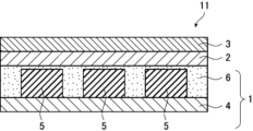
- FIG. 1 is a schematic cross-sectional view showing one embodiment of a light emitting device according to the present invention.
- FIG. 2 is a schematic cross-sectional view showing another example of the embodiment of the light emitting device of the present invention.
- FIG. 3 is a schematic cross-sectional view showing another example of the embodiment of the light emitting device of the present invention.
- FIG. 4 is a schematic cross-sectional view showing another example of the embodiment of the light emitting device of the present invention.
- each component may be used alone or in combination of two or more substances corresponding to each component.
- the content of the component refers to the total content of the substances used in combination, unless otherwise specified.
- Re( ⁇ ) and Rth( ⁇ ) respectively represent the in-plane retardation and the retardation in the thickness direction at a wavelength ⁇ , which is 550 nm unless otherwise specified.
- the light emitting device of the present invention includes a display element, a ⁇ /4 plate, and a polarizer.
- the display element of the light-emitting device of the present invention has a substrate, a plurality of light-emitting elements arranged on the substrate, and a coloring layer containing at least one colorant selected from the group consisting of pigments and dyes, arranged in at least a portion of an area on the substrate where there are no light-emitting elements.
- the average visible light transmittance of the polarizer included in the light emitting device of the present invention is 44 to 55%.
- a polarizer having an average visible light transmittance of 44 to 55% is used, and a display element having a colored layer disposed in at least a part of an area on a substrate where no light-emitting element is present is used, thereby improving the light utilization efficiency of the light-emitting device and suppressing external light reflection.
- the reason why such an effect is achieved is not clear in detail, but the inventors speculate as follows. In other words, it is believed that by using a polarizer with an average visible light transmittance of 44 to 55%, it is possible to improve the light utilization efficiency while ensuring polarization performance.
- a light-emitting device 11 shown in FIG. 1 includes a display element 1 , a ⁇ /4 plate 2 , and a polarizer 3 .
- the display element 1 also has a substrate 4, a plurality of light-emitting elements 5 arranged on the substrate 4, and a colored layer 6 arranged on at least a part of an area on the substrate 4 where no light-emitting elements 5 are present.
- the colored layer 6 may be disposed over the entire area of the substrate 4 where no light-emitting element 5 is present, as shown in FIG. 1, or may be disposed so as to cover the light-emitting element 5.
- the light-emitting device 12 shown in FIG. 2 includes a display element 1 , a ⁇ /4 plate 2 , and a polarizer 3 .
- the display element 1 also has a substrate 4, a plurality of light-emitting elements 5 arranged on the substrate 4, a colored layer 6a arranged over the entire region of the substrate 4 where there are no light-emitting elements 5, and a transparent layer 7 containing neither a pigment nor a dye, arranged on the colored layer 6a and arranged so as to cover the light-emitting elements 5.
- the transparent layer 7 may be a low-concentration colored layer containing at least one colorant selected from the group consisting of pigments and dyes at a concentration lower than the concentration of the colorant in the colored layer 6a.
- the colored layer 6a is preferably disposed so that the average thickness thereof is smaller than the average height of the light emitting element 5.
- the light-emitting device 12 shown in FIG. 3 includes a display element 1 , a ⁇ /4 plate 2 , and a polarizer 3 .
- the display element 1 also has a substrate 4, a plurality of light-emitting elements 5 arranged on the substrate 4, a colored layer 6b arranged in a portion of an area on the substrate 4 where there are no light-emitting elements 5, and a transparent layer 7 containing neither a pigment nor a dye and arranged so as to cover the light-emitting elements 5.
- the transparent layer 7 may be a low-concentration colored layer containing at least one colorant selected from the group consisting of pigments and dyes at a concentration lower than the concentration of the colorant in the colored layer 6a.
- a light emitting device 14 shown in FIG. 4 includes a display element 1, a ⁇ /4 plate 2, and a polarizer 3a.
- the display element 1 also has a substrate 4, a plurality of light-emitting elements 5 arranged on the substrate 4, and a colored layer 6 arranged on at least a part of an area on the substrate 4 where no light-emitting elements 5 are present.
- the polarizer 3a preferably has an opening in a region overlapping with the light emitting element 5 when the light emitting device 14 is observed from the viewing side.
- the display element of the light-emitting device of the present invention has a substrate, a plurality of light-emitting elements arranged on the substrate, and a colored layer containing at least one colorant selected from the group consisting of pigments and dyes, arranged in at least a portion of an area on the substrate where there are no light-emitting elements.
- Substrate> As the substrate of the display element, various element substrates such as a resin film or a glass substrate that are used as element substrates in conventional organic EL display devices, inorganic EL display devices, and the like can be used.
- Examples of the multiple light-emitting elements included in the display element include an R light-emitting element that emits red light, a G light-emitting element that emits green light, and a B light-emitting element that emits blue light. Moreover, it is preferable that a large number of R, G and B light-emitting elements are arranged two-dimensionally, similarly to known display elements.
- the area ratio of the light-emitting elements in the display element is not particularly limited, but is preferably 30% or less, more preferably 10% or less, and even more preferably 3% or less.
- the light-emitting element is an inorganic EL light-emitting element (so-called LED), because sufficient brightness can be achieved even if the area ratio of the light-emitting element in the display element is reduced.
- the light-emitting element is covered with a transparent layer that does not contain either a pigment or a dye, or a low-concentration colored layer that contains at least one colorant selected from the group consisting of pigments and dyes at a concentration lower than the concentration of the colorant in the colored layer described below, and it is more preferable that the entire light-emitting element is covered with the above-mentioned transparent layer or the above-mentioned low-concentration colored layer.
- the transparent layer or low-concentration colored layer being disposed on at least a portion of the surface or side surface of the light-emitting element. It is more preferable that the concentration (C2) of the colorant in the transparent layer or the low-concentration colored layer and the concentration (C1) of the colorant in the colored layer satisfy the following formula (1). 0 ⁇ C2/C1 ⁇ 0.3 (1)
- the colored layer of the display element is a layer containing at least one colorant selected from the group consisting of pigments and dyes, and is disposed in at least a part of the region on the substrate where the light emitting element is not present.
- the colored layer may be disposed over the entire area of the substrate where no light-emitting element is present, or may be disposed so as to cover the light-emitting element.
- pigments which are a type of colorant, include carbon black, chrome yellow, Hansa yellow, benzidine yellow, threne yellow, quinoline yellow, pigment yellow, permanent orange GTR, pyrazolone orange, Balkan orange, Watch Young Red, permanent red, brilliant carmine 3B, brilliant carmine 6B, DuPont oil red, pyrazolone red, lithol red, rhodamine B lake, lake red C, pigment red, rose bengal, aniline blue, ultramarine blue, chalco oil blue, methylene blue chloride, phthalocyanine blue, pigment blue, phthalocyanine green, and malachite green oxalate. These may be used alone or in combination of two or more.
- Dyes which are a type of colorant, include, for example, pyrazole azo compounds, pyrromethene compounds, anilino azo compounds, triphenylmethane compounds, anthraquinone compounds, benzylidene compounds, oxonol compounds, pyrazolotriazole azo compounds, pyridone azo compounds, cyanine compounds, phenothiazine compounds, and pyrrolopyrazole azomethine compounds, and these may be used alone or in combination of two or more.
- the content of the colorant in the colored layer is preferably 0.5 to 50% by mass, more preferably 1 to 40% by mass, and even more preferably 2 to 30% by mass.
- the emission loss rate of the colored layer is preferably 1 to 20%, and more preferably 5 to 20%, for the reason that the light utilization efficiency is further improved.
- the luminance loss rate can be calculated as the ratio (reduction rate) of the reduction in the luminance of a display element having a colored layer to the luminance of a display element having a layer (transparent layer) without the colorant contained in the colored layer.
- the method for adjusting the luminescence loss rate of the colored layer is not particularly limited, but may be, for example, a method for adjusting the content of a coloring agent contained in the colored layer.
- the average thickness of the colored layer (hereinafter also abbreviated as “average thickness of the colored layer”) is smaller than the average height of the light emitting element (hereinafter also abbreviated as “average height of the light emitting element”).
- the average thickness of the colored layer and the average height of the light emitting element are both expressed in the same unit ( ⁇ m).
- the average thickness of the colored layer is more preferably 1 ⁇ 2 or less, and even more preferably 1 ⁇ 4 or less, of the average height of the light emitting element.
- the average thickness of the colored layer is the arithmetic average of the thicknesses measured at any five or more points of the colored layer
- the average height of the light-emitting element is the arithmetic average of the heights measured at multiple light-emitting elements.
- the ⁇ /4 plate of the light emitting device of the present invention is a plate having a ⁇ /4 function, specifically, a plate having the function of converting linearly polarized light of a certain wavelength into circularly polarized light (or circularly polarized light into linearly polarized light).
- specific examples of the ⁇ /4 plate having a single layer structure include a stretched polymer film and a retardation film having an optically anisotropic layer having ⁇ /4 function provided on a support
- specific examples of the ⁇ /4 plate having a multilayer structure include a broadband ⁇ /4 plate formed by laminating a ⁇ /4 plate and a ⁇ /2 plate.
- the optically anisotropic layer having ⁇ /4 function it is also preferable to have a layer formed by fixing a uniformly aligned liquid crystal compound.
- a layer in which a rod-shaped liquid crystal compound is uniformly aligned horizontally to the in-plane direction, or a layer in which a discotic liquid crystal compound is uniformly aligned perpendicularly to the in-plane direction can be used.
- a rod-shaped liquid crystal compound having reverse dispersion can be uniformly aligned and fixed to produce an optically anisotropic layer having reverse dispersion.
- the polarizer in the light-emitting device of the present invention is not particularly limited as long as it has the function of converting light into a specific linearly polarized light and has an average visible light transmittance of 44 to 55%, and conventionally known absorptive polarizers and reflective polarizers can be used.
- the average visible light transmittance means the arithmetic mean value of the transmittance at 5 nm intervals in the visible light region (wavelength 400 nm to 700 nm).
- a spectrophotometer for example, a multichannel spectrometer (manufactured by OCEAN OPTICS, product name "QE65000") is used to measure the transmittance.
- the average visible light transmittance of the polarizer is preferably from 47 to 55%, and more preferably from 50 to 55%.
- the polarizer is preferably an optically absorptive anisotropic film containing a liquid crystal compound and a dichroic substance, and more preferably an optically absorptive anisotropic film in which the orientation states of the liquid crystal compound and the dichroic substance are fixed.
- the liquid crystal compound and dichroic substance contained in the light absorption anisotropic film, as well as any optional components, will be described below.
- liquid crystal compound either a high molecular weight liquid crystal compound or a low molecular weight liquid crystal compound can be used.
- polymeric liquid crystal compound refers to a liquid crystal compound having a repeating unit in the chemical structure.
- low molecular weight liquid crystal compound refers to a liquid crystal compound that does not have a repeating unit in its chemical structure.
- the polymer liquid crystal compound include the thermotropic liquid crystal polymer described in JP-A-2011-237513 and the polymer liquid crystal compound described in paragraphs [0012] to [0042] of WO 2018/199096.
- Examples of the low molecular weight liquid crystal compound include the liquid crystal compounds described in paragraphs [0072] to [0088] of JP-A-2013-228706, and among them, liquid crystal compounds exhibiting smectic properties are preferable.
- Such liquid crystal compounds include those described in paragraphs [0019] to [0140] of International Publication No. 2022/014340, the descriptions of which are incorporated herein by reference.
- the content of the liquid crystal compound is preferably 50 to 99% by mass, and more preferably 75 to 90% by mass, based on the total mass of the light absorbing anisotropic film.
- the dichroic substance means a dye having different absorbance depending on the direction.
- the dichroic substance may or may not exhibit liquid crystallinity.
- the dichroic substance is not particularly limited, and examples thereof include visible light absorbing substances (dichroic dyes), luminescent substances (fluorescent substances, phosphorescent substances), ultraviolet absorbing substances, infrared absorbing substances, nonlinear optical substances, carbon nanotubes, and inorganic substances (e.g., quantum rods), and any conventionally known dichroic substance (dichroic dye) can be used.
- a dichroic azo dye compound as the dichroic substance, and it is more preferable to use a dichroic azo dye compound having a thienothiazole skeleton.
- the dichroic azo dye compound means an azo dye compound whose absorbance varies depending on the direction.
- the dichroic azo dye compound may or may not exhibit liquid crystallinity. When the dichroic azo dye compound exhibits liquid crystallinity, it may exhibit either nematic or smectic properties.
- the temperature range in which the liquid crystal phase is exhibited is preferably room temperature (about 20 to 28°C) to 300°C, and more preferably 50 to 200°C from the viewpoints of handling and manufacturing suitability.
- three or more dichroic azo dye compounds may be used in combination.
- a first dichroic azo dye compound a second dichroic azo dye compound, and at least one dye compound (a third dichroic azo dye compound) having a maximum absorption wavelength in the wavelength range of 380 nm or more and less than 455 nm in combination.
- the dichroic azo dye compound preferably has a crosslinkable group.
- the crosslinkable group include a (meth)acryloyl group, an epoxy group, an oxetanyl group, and a styryl group, and among these, a (meth)acryloyl group is preferable.
- (meth)acryloyl group refers to an "acryloyl group” or a "methacryloyl group”.
- the relationship between the maximum intensity Imax in the thickness direction of the optically absorptive anisotropic film and the intensity Isur at the surface of the optically absorptive anisotropic film corresponding to the viewing side of the light emitting device, for a signal derived from a dichroic substance detected by time-of-flight secondary ion mass spectrometry, satisfies the following formula (2):
- an example of an embodiment that satisfies the following formula (2) is an embodiment in which the dichroic substance present in the optically absorptive anisotropic film is unevenly distributed on the ⁇ /plate side of the optically absorptive anisotropic film. 2.0 ⁇ Imax/Isur... (2)
- TOF-SIMS measurement method In the present invention, the measurement by TOF-SIMS is performed as follows. (1) Apparatus and conditions Apparatus: TOF-SIMS 5 (ION-TOF) Depth direction analysis: Combined use of Ar ion sputtering Measurement range: Raster scan of 128 points in one direction and the perpendicular direction Polarity: posi, nega (2) Intensity Isur and maximum intensity Imax The optically absorptive anisotropic film to be measured is measured in the thickness direction at a constant speed from the visible side surface of the optically absorptive anisotropic film to the surface opposite the visible side surface, and the strength is measured in each of the following regions.
- (Intensity Isur) The average value of the mass spectrometry intensity of the fragments derived from the dichroic substance in a region of 1% from the viewing side surface of the optically absorptive anisotropic film (average value of the intensity from the baseline) is defined as the intensity Isur at the viewing side surface.
- (Maximum intensity Imax) The maximum intensity (intensity from the baseline) of the mass spectrometry of the fragments derived from the dichroic material in a region of 98% of the total thickness excluding 1% of the total thickness from each surface is defined as the maximum intensity Imax in the thickness direction.
- the viewing side surface of the above-mentioned optically absorptive anisotropic film i.e., the interface with the adjacent layer
- the viewing side surface of the above-mentioned optically absorptive anisotropic film can be identified as the point where the mass spectrometry intensity of the fragment derived from the liquid crystal compound detected from the optically absorptive anisotropic film intersects with the mass spectrometry intensity of the fragment derived from the compound that is most abundant among the fragments detected from the adjacent layer.
- the mass spectrometry intensity of a fragment derived from a dichroic substance having a maximum absorption wavelength in the wavelength range of 500 to 650 nm (hereinafter referred to as "target dichroic substance" in this paragraph) is measured, and when the optically absorptive anisotropic film contains two or more dichroic substances, the mass spectrometry intensity of a fragment derived from the dichroic substance having the greatest absorbance among the target dichroic substances is measured.
- the amount of the dichroic substance present per unit volume in the light absorptive anisotropic film is preferably 100 mg/cm 3 or less, more preferably 40 to 95 mg/cm 3 , and even more preferably 50 to 90 mg/cm 3.
- the total amount of the plurality of dichroic substances is preferably within the above-mentioned range.
- the amount (mg/cm 3 ) of the dichroic substance present can be obtained by measuring a solution in which an optical laminate having an optical absorption anisotropic film is dissolved, or an extract obtained by immersing the optical laminate in a solvent, by high performance liquid chromatography (HPLC), but is not limited to the above method. Quantification can be performed by using the dichroic substance contained in the optical absorption anisotropic film as a standard sample.
- One example of a method for calculating the amount (mg/ cm3 ) of dichroic substance is to calculate the volume by multiplying the thickness of the optically absorptive anisotropic film obtained from a microscopic image of the cross section of the optical laminate by the area of the optical laminate used to measure the amount of dye, and then dividing the volume by the amount of dye measured by HPLC to calculate the dye content.
- the relationship between the average visible light transmittance Ta of the polarizer in the region overlapping with the light-emitting element and the average visible light transmittance Tb of the polarizer in the region other than the above region satisfies the following formula (3).
- a specific embodiment that satisfies the following formula (3) is, as shown in FIG. 4, an embodiment in which an opening is provided in a region of the polarizer that overlaps with the light-emitting element when the light-emitting device is observed from the viewing side. 1.5 ⁇ Ta/Tb ⁇ 2.5 (3)
- the above core layer cellulose acylate dope and the above outer layer cellulose acylate dope were filtered through a filter paper having an average pore size of 34 ⁇ m and a sintered metal filter having an average pore size of 10 ⁇ m, and then the above core layer cellulose acylate dope and the outer layer cellulose acylate dope on both sides were simultaneously cast onto a drum at 20° C. from a casting nozzle (band casting machine).
- the solvent content in the film was about 20% by mass
- the film was peeled off from the drum, both ends in the width direction of the film were fixed with tenter clips, and the film was stretched in the transverse direction at a stretch ratio of 1.1 times while being dried. Thereafter, the obtained film was further dried by conveying it between rolls of a heat treatment device to prepare a transparent support having a thickness of 40 ⁇ m, which was designated as cellulose acylate film A1.
- the photo-alignment film-forming composition B1 described later was continuously applied onto the cellulose acylate film A1 using a wire bar.
- the support on which the coating film was formed was dried with hot air at 140° C. for 120 seconds, and then the coating film was irradiated with polarized ultraviolet light (10 mJ/cm 2 , using an ultra-high pressure mercury lamp) to form a photo-alignment film B1, thereby obtaining a TAC (triacetyl cellulose) film with a photo-alignment film.
- the thickness of the photo-alignment film B1 was 0.25 ⁇ m.
- Polymer PA-1 (wherein the numerical value for each repeating unit represents the content (mass %) of each repeating unit relative to the total repeating units.)
- ⁇ Orientation process> The coating was then heated at 140° C. for 15 seconds, and the coating was then cooled to room temperature (23° C.). The coating was then heated to 75° C. for 60 seconds and cooled again to room temperature. Thereafter, an LED lamp (center wavelength 365 nm) was used to irradiate the film with an illuminance of 200 mW/ cm2 for 2 seconds to produce a light absorption anisotropic film C1 (polarizer) (thickness: 0.4 ⁇ m) on the photo-alignment film B1.
- polarizer polarizer
- the transmittance of the optically absorptive anisotropic film C1 in the wavelength region of 280 to 780 nm was measured by a spectrophotometer, and the average visible light transmittance was 50%.
- the absorption axis of the optically absorptive anisotropic film C1 was perpendicular to the width direction of the cellulose acylate film A1.
- the amount of the dichroic substance present per unit volume in the optically absorptive anisotropic film C1 was confirmed by the above-mentioned method and was found to be 170 mg/cm 3 .
- Liquid crystal compound (L-1) (In the following formula, the numerical values ("59", “15”, “26") shown for each repeating unit represent the content (% by mass) of each repeating unit relative to the total repeating units.)
- Liquid crystal compound (L-2) [a mixture of the following liquid crystal compounds (RA), (RB), and (RC) in a mass ratio of 84:14:2]
- Adhesion improver (A-1) Adhesion improver (A-1)
- Surfactant (F-1) (In the following formula, the numerical value for each repeating unit represents the content (mass %) of each repeating unit relative to the total repeating units.)
- the coating solution D1 for forming the oxygen barrier layer having the following composition was continuously applied with a wire bar. Then, by drying with hot air at 80° C. for 5 minutes, a laminate having an oxygen barrier layer D1 made of polyvinyl alcohol (PVA) having a thickness of 1.0 ⁇ m formed thereon, that is, a laminate CP1 having a cellulose acylate film A1 (transparent support), a photo-alignment film B1, an optically absorptive anisotropic film C1, and an oxygen barrier layer D1 adjacent to each other in this order, was obtained.
- PVA polyvinyl alcohol
- Modified polyvinyl alcohol in the following formula, the numerical value for each repeating unit represents the content (mass %) of each repeating unit relative to the total repeating units.
- composition E1 for forming a photo-alignment film having the following composition was continuously applied onto the above-mentioned cellulose acylate film A1 using a wire bar.
- the support on which the coating film was formed was dried with hot air at 140° C. for 120 seconds, and then the coating film was irradiated with polarized ultraviolet light (10 mJ/cm 2 , using an ultra-high pressure mercury lamp) to form a photo-alignment film E1 with a thickness of 0.2 ⁇ m, thereby obtaining a TAC film with a photo-alignment film.
- Polymer PA-2 (wherein the numerical value for each repeating unit represents the content (mass %) of each repeating unit relative to the total repeating units.)
- the composition F1 having the following composition was applied onto the photo-alignment film E1 using a bar coater.
- the coating film formed on the photo-alignment film E1 was heated to 120° C. with hot air, and then cooled to 60° C., and then irradiated with 100 mJ/cm 2 ultraviolet light at a wavelength of 365 nm using a high-pressure mercury lamp under a nitrogen atmosphere, and then irradiated with 500 mJ/cm 2 ultraviolet light while heating to 120° C., thereby fixing the alignment of the liquid crystal compound and producing a TAC film having a positive A plate F1.
- the positive A plate F1 had a thickness of 2.5 ⁇ m and an Re(550) of 144 nm, and was a plate having a ⁇ /4 function. The positive A plate also satisfied the relationship Re(450) ⁇ Re(550) ⁇ Re(650). Re(450)/Re(550) was 0.82.
- Polymerizable liquid crystal compound LA-1 (tBu represents a tert-butyl group)
- Polymerizable liquid crystal compound LA-4 (Me represents a methyl group)
- Leveling agent T-1 (wherein the numerical value for each repeating unit represents the content (mass %) of each repeating unit relative to the total repeating units.)
- TAC film having positive C-plate H1 As the temporary support, the above-mentioned cellulose acylate film A1 was used. The cellulose acylate film A1 was passed through a dielectric heating roll at a temperature of 60°C to raise the surface temperature of the film to 40°C, and then an alkaline solution having the composition shown below was applied to one side of the film in an amount of 14 ml/ m2 using a bar coater, heated to 110°C, and transported under a steam-type far-infrared heater manufactured by Noritake Co., Limited for 10 seconds. Next, 3 ml/ m2 of pure water was applied onto the film using the same bar coater. Next, after repeating washing with a fountain coater and draining with an air knife three times, the film was transported to a drying zone at 70° C. for 10 seconds and dried to prepare an alkaline saponified cellulose acylate film A1.
- composition G1 for forming a photo-alignment film having the following composition was continuously applied onto the above-mentioned alkaline saponification-treated cellulose acylate film A1 using a #8 wire bar.
- the resulting film was dried with hot air at 60°C for 60 seconds and then with hot air at 100°C for 120 seconds to form a photo-alignment film G1.
- a coating solution H1 for forming a positive C plate having the following composition was applied onto a photo-alignment film G1, and the resulting coating film was aged at 60° C. for 60 seconds.
- the coating film was then irradiated with ultraviolet light at 1000 mJ/cm 2 using an air-cooled metal halide lamp (manufactured by Eye Graphics Co., Ltd.) at 70 mW/cm 2 under air to fix the alignment state, thereby vertically aligning the liquid crystal compound, and a TAC film having a positive C plate H1 with a thickness of 0.5 ⁇ m was produced.
- the Rth(550) of the obtained positive C plate was ⁇ 60 nm.
- Compound B03 (wherein the numerical value for each repeating unit represents the content (mass%) of each repeating unit relative to the total repeating units.)
- an acrylate polymer was prepared according to the following procedure.
- a reaction vessel equipped with a cooling tube, a nitrogen inlet tube, a thermometer, and a stirrer 95 parts by mass of butyl acrylate and 5 parts by mass of acrylic acid were polymerized by a solution polymerization method to obtain an acrylate polymer (NA1) having an average molecular weight of 2,000,000 and a molecular weight distribution (Mw/Mn) of 3.0.
- acrylate polymer (NA1) was used to prepare acrylate adhesives with the following compositions. These compositions were applied to a separate film surface-treated with a silicone release agent using a die coater, dried for 1 minute in a 90°C environment, and irradiated with ultraviolet (UV) rays under the following conditions to obtain the following acrylate adhesives N1 and N2 (adhesive layers).
- UV ultraviolet
- the compositions and film thicknesses of the acrylate adhesives are shown below.
- ⁇ UV irradiation conditions> Fusion electrodeless lamp H bulb Illuminance: 600mW/ cm2 , light output: 150mJ/ cm2 UV illuminance and light quantity were measured using "UVPF-36" manufactured by Eye Graphics.
- (A) Polyfunctional acrylate monomer: tris(acryloyloxyethyl)isocyanurate, molecular weight 423, trifunctional type (manufactured by Toagosei Co., Ltd., product name "Aronix M-315")
- UV adhesive composition having the following composition was prepared.
- ⁇ UV adhesive composition ------------------------------------------------------------------------ ⁇ 70 parts by mass of CEL2021P (manufactured by Daicel Corporation) ⁇ 20 parts by mass of 1,4-butanediol diglycidyl ether ⁇ 10 parts by mass of 2-ethylhexyl glycidyl ether ⁇ 2.25 parts by mass of CPI-100P ⁇
- the retardation side of the TAC film having the positive A plate F1 and the retardation side of the TAC film having the positive C plate H1 were laminated together by UV irradiation of 600 mJ/ cm2 using the UV adhesive composition.
- the thickness of the UV adhesive layer was 3 ⁇ m.
- the surfaces to be laminated with the UV adhesive were each subjected to corona treatment.
- the photo-alignment film E1 and the cellulose acylate film A1 on the positive A plate F1 side were removed to obtain a retardation plate AC1.
- the layer structure of the retardation plate AC1 is the positive A plate F1, the UV adhesive layer, the positive C plate H1, the photo-alignment film G1 and the cellulose acylate film A1.
- the oxygen barrier layer D1 side of the laminate CP1 was bonded to the support side of the low reflection surface film CV-LC5 (manufactured by Fujifilm Corporation) using the adhesive N1.
- the cellulose acylate film A1 contained in the laminate CP1 was removed, and the removed surface and the positive A plate F1 side of the retardation plate AC1 were bonded to each other using the adhesive N1.
- the photo-alignment film G1 and the cellulose acylate film A1 on the positive C plate H1 side contained in the retardation plate AC1 were removed to prepare a laminate CPAC1.
- the layer structure of the laminate CPAC1 is a low reflection surface film CV-LC5, an adhesive layer N1, an oxygen barrier layer D1, a light absorption anisotropic film C1, a photoalignment film B1, an adhesive layer N1, a positive A plate F1, a UV adhesive layer, and a positive C plate H1.
- LED display device 1 Three-color light-emitting LEDs (manufactured by ROHM Co., Ltd., PICOLED model number: SMLP34RGB) were arranged in a two-dimensional lattice pattern on a printed circuit board so that the area ratio of the LEDs (light-emitting elements) was 30%, and the LEDs were embedded in a colored layer 1 made of a black matrix material. Next, the luminance was measured from a distance of 700 mm using a spectrophotometer (SR3, manufactured by Topcon Technohouse). The luminance loss rate for a sample prepared in the same manner except that a transparent layer made of a transparent resin material was used instead of the colored layer 1 was 1%. Next, the positive C plate H1 side of the laminate CPAC1 prepared above was attached onto the colored layer 1 while preventing air from entering, to prepare an LED display device (display device 1).
- SR3 spectrophotometer
- Example 2 An LED display device (display device 2) was produced according to the same procedure as in Example 1, except that an optically absorptive anisotropic film having a thickness adjusted to have an average visible light transmittance of 44% was used using the optically absorptive anisotropic film-forming composition C1 instead of the optically absorptive anisotropic film C1.
- Example 3 An LED display device (display device 3) was produced in the same manner as in Example 1, except that the colored layer 1 was replaced with a colored layer having a light emission loss rate of 20%.
- Example 4 An LED display device (display device 4) was produced according to the same procedure as in Example 1, except that a colored layer having an emission loss rate of 20% was used instead of the colored layer 1, and a light-absorption anisotropic film having a thickness adjusted to have an average visible light transmittance of 44% using the light-absorption anisotropic film-forming composition C1 was used instead of the light-absorption anisotropic film C1.
- Example 5 An LED display device (display device 5) was produced according to the same procedure as in Example 1, except that a colored layer having a luminous loss rate of 10% was used instead of the colored layer 1, and a light-absorption anisotropic film having a thickness adjusted to have an average visible light transmittance of 47% using the light-absorption anisotropic film-forming composition C1 was used instead of the light-absorption anisotropic film C1.
- Example 6 An LED display device (display device 6) was produced according to the same procedure as in Example 1, except that, instead of the colored layer 1, a colored layer having a light emission loss rate of 10% was formed to a height of 1/5 of the height of the light emitting element from the printed circuit board, and a transparent layer not having a black matrix material was formed on the colored layer to embed the light emitting element.
- Example 7 An LED display device (display device 7) was produced in the same manner as in Example 1, except that, instead of the colored layer 1, a colored layer having a light emission loss rate of 10% was formed so as not to be provided around the light-emitting element, and a transparent layer not having a black matrix material was formed around the light-emitting element to embed the light-emitting element.
- Example 8 An LED display device (display device 8) was produced by the same procedure as in Example 1, except that an optically absorptive anisotropic film formed using composition C2 for forming an optically absorptive anisotropic film having the following composition was used, and a colored layer having a luminescence loss rate of 10% was used instead of colored layer 1.
- the amount of dichroic material present per unit volume in the optically absorptive anisotropic film formed was confirmed by the above-mentioned method and was found to be 170 mg/ cm3 .
- Example 8 the signal derived from the dichroic substance detected by time-of-flight secondary ion mass spectrometry was confirmed by the method described above, and it was confirmed that the relationship between the maximum intensity Imax in the thickness direction of the optically absorptive anisotropic film and the intensity Isur at the surface of the optically absorptive anisotropic film corresponding to the viewing side of the light-emitting device satisfied the following formula (2). 2.0 ⁇ Imax/Isur... (2)
- Example 9 Regarding the preparation of the laminate CPAC1, the laminate was prepared according to the same procedure as in Example 1, except that the transparent support, photo-alignment film, and light absorption anisotropic film shown below were used, and that the step of removing the transparent support was not included. Next, using the produced laminate, an LED display device (display device 9) was produced in the same manner as in Example 1, except that the colored layer 1 was replaced with a colored layer having a luminous loss rate of 10%.
- composition E2 for forming a photoalignment film was prepared according to the following formulation, dissolved for 1 hour with stirring, and filtered through a 0.45 ⁇ m filter. -------------------------------------------------------------------------------------------------------------------------------------------------------------------------------------------------------------------------------------------------------------------------------------------------------------------------------------------------------------------------------------------------------------------------------------------------------------------------------------------------------------------------------------------------------------------------------------------------------------------------------------------------------
- Photoactive compound E-4 (weight average molecular weight: 51,000)
- composition P1 for forming an optically absorptive anisotropic film was prepared according to the following formulation, which was then dissolved by heating at 80° C. for 2 hours with stirring, and filtered through a 0.45 ⁇ m filter.
- Liquid crystal compound M1 (compound A/compound B mixed at 75/25)
- the composition E2 for forming a photo-alignment film was applied onto a cellulose triacetate film TJ40 (manufactured by Fujifilm: thickness 40 ⁇ m) as a transparent support, and dried for 2 minutes at 60° C. Thereafter, the resulting coating film was irradiated with linearly polarized ultraviolet light (100 mJ/cm 2 ) using a polarized ultraviolet light exposure device, to produce a photo-alignment film E2.
- the optically absorptive anisotropic film-forming composition P1 was applied onto the obtained photoalignment film E2 with a wire bar. Next, the obtained coating film was heated at 120° C. for 60 seconds and cooled to room temperature.
- optically absorptive anisotropic film P1 having a thickness of 1.7 ⁇ m. It was confirmed that the liquid crystal of the optically absorptive anisotropic film was in a smectic B phase and had an average visible light transmittance of 50%. The amount of the dichroic material present per unit volume in the optically absorptive anisotropic film P1 thus formed was confirmed by the above-mentioned method and was found to be 65 mg/cm 3 .
- Example 10 Regarding the preparation of the laminate CPAC1, the laminate was prepared according to the same procedure as in Example 1, except that a transparent support, a photo-alignment film, and a light-absorption anisotropic film were used as described below, and that a step of removing the photo-alignment film was included.
- an LED display device (display device 10) was produced using the produced laminate in the same manner as in Example 1, except that colored layer 1 was replaced with a colored layer having a luminous loss rate of 10%.
- a polymer coating solution having the following composition was continuously applied onto a 40 ⁇ m-thick TAC substrate (manufactured by Fujifilm Corporation, TG40) using a wire bar #8. The substrate was then dried for 2 minutes with hot air at 100° C. to obtain a support having a 0.8 ⁇ m-thick polyvinyl alcohol (PVA) polymer film formed on the TAC substrate.
- PVA polyvinyl alcohol
- the modified polyvinyl alcohol was added to the polymer coating solution so that the solid content concentration was 4% by mass.
- Modified polyvinyl alcohol in the following formula, the numerical value for each repeating unit represents the content (mass %) of each repeating unit relative to the total repeating units.
- the obtained coating film was irradiated with linearly polarized ultraviolet light (illuminance 4.5 mW/cm 2 , cumulative irradiation amount 300 mJ/cm 2 ) using a polarized ultraviolet light exposure device (first light irradiation) to prepare a photo-alignment film having an alignment control force in the horizontal direction.
- the thickness of the photo-alignment film was 50 nm.
- the obtained photo-alignment film was irradiated with unpolarized ultraviolet light (illuminance 4.5 mW/ cm2 , cumulative exposure dose 2000 mJ/ cm2 ) through a photomask in a direction perpendicular to the film surface (second light irradiation) to produce a pattern-exposed photo-alignment film.
- the mask pattern of the mask had a light-shielding portion corresponding to the position of the light-emitting element (area ratio 30%) of the LED display device (display device 1) described above, and had a light-transmitting portion and a light-shielding portion.
- a composition F1 for forming an optically absorptive anisotropic film having the following composition was continuously coated with a wire bar to form a coating layer F.
- the coating layer F was heated at 140° C. for 15 seconds, and then the coating layer F was cooled to room temperature (23° C.). It was then heated at 75° C. for 60 seconds and cooled again to room temperature.
- an LED lamp (center wavelength 365 nm) was used to irradiate the film with an illuminance of 200 mW/ cm2 for 2 seconds to produce an optically absorptive anisotropic film having a visible light average transmittance of 55%, which has region A and region B with different inclinations of the absorption axis relative to the film surface on the pattern-exposed alignment film.
- composition of composition F1 for forming optically absorptive anisotropic film ------------------------------------------------------------------------------------------------------------------------------------------------------------------------------------------------------------------------------------------------------------------------------------------------------------------------------------------------------------------------------------------------------------------------------------------------------------------------------------------------------------------------------------------------------------------------------------------------------------------------------------------------------------------------------------------------------------------------------
- Dichroic substance C-1 (maximum absorption wavelength: 570 nm)
- Dichroic substance M-1 (maximum absorption wavelength: 466 nm)
- Dichroic material Y-1 (maximum absorption wavelength: 417 nm)
- Liquid crystal compound L-2 [a mixture of the following liquid crystal compounds (RA), (RB), and (RC) in a mass ratio of 84:14:2]
- Surfactant S-1 (In the following formula, the numerical value for each repeating unit indicates the content (mass %) of each repeating unit relative to the total repeating units.)
- Example 10 when the fabricated LED display device (display device 10) was observed from the viewing side, the relationship between the average visible light transmittance Ta of the polarizer in the region overlapping with the light-emitting element and the average visible light transmittance Tb of the polarizer in the region other than the above region was examined, and it was found that the following formula (3) was satisfied. 1.5 ⁇ Ta/Tb ⁇ 2.5 (3)
- Example 1 An LED display device (display device C1) was produced according to the same procedure as in Example 1, except that a transparent layer made of a transparent resin material was used instead of the colored layer 1, and an optically absorptive anisotropic film having an average visible light transmittance of 47% was used instead of the optically absorptive anisotropic film C1.
- Example 2 An LED display device (display device C2) was produced according to the same procedure as in Example 1, except that a colored layer having a light emission loss rate of 40% was used instead of the colored layer 1, and the step of bonding the laminate CPAC1 onto the colored layer 1 was omitted. That is, a light-emitting device having no ⁇ /4 plate or polarizer was produced.
- Example 3 An LED display device (display device C3) was produced according to the same procedure as in Example 1, except that a colored layer having a luminous loss rate of 10% was used instead of the colored layer 1, and a light absorbing anisotropic film having an average visible light transmittance of 56% was used instead of the light absorbing anisotropic film C1.
- Example 4 An LED display device (display device C4) was produced according to the same procedure as in Example 1, except that a colored layer having a luminous loss rate of 20% was used instead of the colored layer 1, and a light absorbing anisotropic film having an average visible light transmittance of 42% was used instead of the light absorbing anisotropic film C1.
Landscapes
- Physics & Mathematics (AREA)
- General Physics & Mathematics (AREA)
- Optics & Photonics (AREA)
- Chemical & Material Sciences (AREA)
- Crystallography & Structural Chemistry (AREA)
- Engineering & Computer Science (AREA)
- Theoretical Computer Science (AREA)
- Electroluminescent Light Sources (AREA)
Priority Applications (2)
| Application Number | Priority Date | Filing Date | Title |
|---|---|---|---|
| JP2024552925A JPWO2024090167A1 (https=) | 2022-10-28 | 2023-10-05 | |
| US19/091,402 US20250228056A1 (en) | 2022-10-28 | 2025-03-26 | Light emitting device |
Applications Claiming Priority (2)
| Application Number | Priority Date | Filing Date | Title |
|---|---|---|---|
| JP2022-173190 | 2022-10-28 | ||
| JP2022173190 | 2022-10-28 |
Related Child Applications (1)
| Application Number | Title | Priority Date | Filing Date |
|---|---|---|---|
| US19/091,402 Continuation US20250228056A1 (en) | 2022-10-28 | 2025-03-26 | Light emitting device |
Publications (1)
| Publication Number | Publication Date |
|---|---|
| WO2024090167A1 true WO2024090167A1 (ja) | 2024-05-02 |
Family
ID=90830509
Family Applications (1)
| Application Number | Title | Priority Date | Filing Date |
|---|---|---|---|
| PCT/JP2023/036396 Ceased WO2024090167A1 (ja) | 2022-10-28 | 2023-10-05 | 発光装置 |
Country Status (3)
| Country | Link |
|---|---|
| US (1) | US20250228056A1 (https=) |
| JP (1) | JPWO2024090167A1 (https=) |
| WO (1) | WO2024090167A1 (https=) |
Citations (6)
| Publication number | Priority date | Publication date | Assignee | Title |
|---|---|---|---|---|
| JP2005063841A (ja) * | 2003-08-13 | 2005-03-10 | Hitachi Ltd | 発光型表示装置 |
| JP2012226906A (ja) * | 2011-04-18 | 2012-11-15 | Canon Inc | 表示装置及びその製造方法 |
| WO2017038927A1 (ja) * | 2015-09-03 | 2017-03-09 | 富士フイルム株式会社 | 有機エレクトロルミネッセンス表示装置 |
| WO2021246148A1 (ja) * | 2020-06-05 | 2021-12-09 | 富士フイルム株式会社 | 光吸収異方性膜、積層体および画像表示装置 |
| WO2022054556A1 (ja) * | 2020-09-09 | 2022-03-17 | 富士フイルム株式会社 | 偏光板、有機エレクトロルミネッセンス表示装置 |
| JP2022115708A (ja) * | 2021-01-28 | 2022-08-09 | 凸版印刷株式会社 | 表示装置及び波長変換基板 |
-
2023
- 2023-10-05 JP JP2024552925A patent/JPWO2024090167A1/ja active Pending
- 2023-10-05 WO PCT/JP2023/036396 patent/WO2024090167A1/ja not_active Ceased
-
2025
- 2025-03-26 US US19/091,402 patent/US20250228056A1/en active Pending
Patent Citations (6)
| Publication number | Priority date | Publication date | Assignee | Title |
|---|---|---|---|---|
| JP2005063841A (ja) * | 2003-08-13 | 2005-03-10 | Hitachi Ltd | 発光型表示装置 |
| JP2012226906A (ja) * | 2011-04-18 | 2012-11-15 | Canon Inc | 表示装置及びその製造方法 |
| WO2017038927A1 (ja) * | 2015-09-03 | 2017-03-09 | 富士フイルム株式会社 | 有機エレクトロルミネッセンス表示装置 |
| WO2021246148A1 (ja) * | 2020-06-05 | 2021-12-09 | 富士フイルム株式会社 | 光吸収異方性膜、積層体および画像表示装置 |
| WO2022054556A1 (ja) * | 2020-09-09 | 2022-03-17 | 富士フイルム株式会社 | 偏光板、有機エレクトロルミネッセンス表示装置 |
| JP2022115708A (ja) * | 2021-01-28 | 2022-08-09 | 凸版印刷株式会社 | 表示装置及び波長変換基板 |
Also Published As
| Publication number | Publication date |
|---|---|
| JPWO2024090167A1 (https=) | 2024-05-02 |
| US20250228056A1 (en) | 2025-07-10 |
Similar Documents
| Publication | Publication Date | Title |
|---|---|---|
| JP6336572B2 (ja) | 反射部材、投映スクリーン、コンバイナ、および、遮熱部材 | |
| JP6952779B2 (ja) | 液晶表示装置 | |
| KR101891421B1 (ko) | 위상차판, 위상차판을 이용한 적층 편광판, 및 위상차판을 이용한 표시 장치 | |
| TW200307162A (en) | Liquid crystal display unit with wide viewing angle | |
| WO2021246286A1 (ja) | 光学要素、画像表示装置、仮想現実表示装置、電子ファインダー、偏光子の製造方法 | |
| US12072570B2 (en) | Display device | |
| KR20160096545A (ko) | 복합 편광판 및 액정 표시 장치 | |
| US10644078B2 (en) | Organic electroluminescence display device having a polarizer comprised of polarization regions | |
| JP2015156032A (ja) | 位相差板、楕円偏光板およびそれを用いた表示装置 | |
| CN101241265A (zh) | 光学装置、图像显示装置、和液晶显示装置 | |
| JP4404624B2 (ja) | 楕円偏光板および画像表示装置 | |
| TW535011B (en) | Improvement of the luminance-contrast performance of a display by an in-tube reflective polarizer | |
| US7746421B2 (en) | Optical element, light condensation backlight system, and liquid crystal display | |
| JP4404623B2 (ja) | 高輝度偏光板および画像表示装置 | |
| WO2024090167A1 (ja) | 発光装置 | |
| JP7727656B2 (ja) | 光学フィルム、光学積層体、および画像表示装置 | |
| JP2016188960A (ja) | 位相差板、位相差板を用いた積層偏光板、および位相差板を用いた表示装置 | |
| JP2017037151A (ja) | 積層体の製造方法 | |
| JP7112432B2 (ja) | 組成物、有機エレクトロルミネッセンス表示素子用位相差膜、有機エレクトロルミネッセンス表示素子用位相差膜の製造方法 | |
| JP2013037336A (ja) | 液晶表示装置 | |
| JP4393972B2 (ja) | 光学素子、集光バックライトシステムおよび液晶表示装置 | |
| JP2016090866A (ja) | 光学フィルムの製造方法ならびにその方法により得られた光学フィルム、該光学フィルムを用いた楕円偏光板および画像表示装置 | |
| WO2026023452A1 (ja) | 光吸収異方性膜、積層体、複合レンズ、ゴーグル型表示装置および光吸収異方性膜の製造方法 | |
| WO2024202820A1 (ja) | 光吸収異方性膜、積層体、複合レンズおよび仮想現実表示装置 | |
| WO2025069986A1 (ja) | 積層体、仮想現実表示装置、積層体の製造方法 |
Legal Events
| Date | Code | Title | Description |
|---|---|---|---|
| 121 | Ep: the epo has been informed by wipo that ep was designated in this application |
Ref document number: 23882376 Country of ref document: EP Kind code of ref document: A1 |
|
| WWE | Wipo information: entry into national phase |
Ref document number: 2024552925 Country of ref document: JP |
|
| NENP | Non-entry into the national phase |
Ref country code: DE |
|
| 122 | Ep: pct application non-entry in european phase |
Ref document number: 23882376 Country of ref document: EP Kind code of ref document: A1 |