WO2024090071A1 - 測距装置、光検出装置、および信号処理装置 - Google Patents
測距装置、光検出装置、および信号処理装置 Download PDFInfo
- Publication number
- WO2024090071A1 WO2024090071A1 PCT/JP2023/033837 JP2023033837W WO2024090071A1 WO 2024090071 A1 WO2024090071 A1 WO 2024090071A1 JP 2023033837 W JP2023033837 W JP 2023033837W WO 2024090071 A1 WO2024090071 A1 WO 2024090071A1
- Authority
- WO
- WIPO (PCT)
- Prior art keywords
- signal
- unit
- beat
- distance measuring
- measuring device
- Prior art date
- Legal status (The legal status is an assumption and is not a legal conclusion. Google has not performed a legal analysis and makes no representation as to the accuracy of the status listed.)
- Ceased
Links
Images



Classifications
-
- G—PHYSICS
- G01—MEASURING; TESTING
- G01S—RADIO DIRECTION-FINDING; RADIO NAVIGATION; DETERMINING DISTANCE OR VELOCITY BY USE OF RADIO WAVES; LOCATING OR PRESENCE-DETECTING BY USE OF THE REFLECTION OR RERADIATION OF RADIO WAVES; ANALOGOUS ARRANGEMENTS USING OTHER WAVES
- G01S17/00—Systems using the reflection or reradiation of electromagnetic waves other than radio waves, e.g. lidar systems
- G01S17/02—Systems using the reflection of electromagnetic waves other than radio waves
- G01S17/06—Systems determining position data of a target
- G01S17/08—Systems determining position data of a target for measuring distance only
- G01S17/32—Systems determining position data of a target for measuring distance only using transmission of continuous waves, whether amplitude-, frequency-, or phase-modulated, or unmodulated
- G01S17/34—Systems determining position data of a target for measuring distance only using transmission of continuous waves, whether amplitude-, frequency-, or phase-modulated, or unmodulated using transmission of continuous, frequency-modulated waves while heterodyning the received signal, or a signal derived therefrom, with a locally-generated signal related to the contemporaneously transmitted signal
-
- G—PHYSICS
- G01—MEASURING; TESTING
- G01S—RADIO DIRECTION-FINDING; RADIO NAVIGATION; DETERMINING DISTANCE OR VELOCITY BY USE OF RADIO WAVES; LOCATING OR PRESENCE-DETECTING BY USE OF THE REFLECTION OR RERADIATION OF RADIO WAVES; ANALOGOUS ARRANGEMENTS USING OTHER WAVES
- G01S7/00—Details of systems according to groups G01S13/00, G01S15/00, G01S17/00
- G01S7/48—Details of systems according to groups G01S13/00, G01S15/00, G01S17/00 of systems according to group G01S17/00
- G01S7/491—Details of non-pulse systems
- G01S7/4911—Transmitters
-
- G—PHYSICS
- G01—MEASURING; TESTING
- G01S—RADIO DIRECTION-FINDING; RADIO NAVIGATION; DETERMINING DISTANCE OR VELOCITY BY USE OF RADIO WAVES; LOCATING OR PRESENCE-DETECTING BY USE OF THE REFLECTION OR RERADIATION OF RADIO WAVES; ANALOGOUS ARRANGEMENTS USING OTHER WAVES
- G01S7/00—Details of systems according to groups G01S13/00, G01S15/00, G01S17/00
- G01S7/48—Details of systems according to groups G01S13/00, G01S15/00, G01S17/00 of systems according to group G01S17/00
- G01S7/497—Means for monitoring or calibrating
Definitions
- This disclosure relates to a distance measuring device, a light detection device, and a signal processing device.
- An FM-CW type laser radar device has been proposed that corrects nonlinear distortion in the frequency modulation characteristics of a transmission signal (Patent Document 1).
- a distance measuring device includes a light source unit capable of outputting a frequency-modulated optical signal, a detection unit capable of detecting a beat signal based on an optical signal and a delayed optical signal, an AD conversion unit capable of sampling the beat signal at each sampling point and performing AD conversion, a signal processing unit capable of generating a first signal related to a correction amount for the frequency of the optical signal based on the beat signal converted into a digital signal, a memory unit capable of storing a plurality of first signals respectively corresponding to a plurality of sampling points, and a control unit capable of controlling the frequency modulation of the optical signal based on the first signal stored in the memory unit.
- An optical detection device includes a detection unit capable of detecting a beat signal based on a frequency-modulated optical signal and a delayed optical signal output from a light source unit, an AD conversion unit capable of sampling the beat signal at each sampling point and performing AD conversion, a signal processing unit capable of generating a first signal related to a correction amount for the frequency of the optical signal based on the beat signal converted into a digital signal, a storage unit capable of storing a plurality of first signals respectively corresponding to a plurality of sampling points, and a control unit capable of controlling the frequency modulation of the optical signal based on the first signal stored in the storage unit.
- a signal processing device includes a detection unit capable of detecting a beat signal based on a frequency-modulated optical signal and a delayed optical signal output from a light source unit, an AD conversion unit capable of sampling the beat signal at each sampling point and performing AD conversion, a signal processing unit capable of generating a first signal related to a correction amount of the frequency of the optical signal based on the beat signal converted into a digital signal, a storage unit capable of storing a plurality of first signals respectively corresponding to a plurality of sampling points, and a control unit capable of outputting a signal for controlling the frequency modulation of the optical signal based on the first signal stored in the storage unit.
- FIG. 1 is a diagram illustrating an example of a schematic configuration of a distance measuring device according to an embodiment of the present disclosure.
- FIG. 2 is a diagram illustrating an example of a signal generated by a distance measuring device according to an embodiment of the present disclosure.
- FIG. 3 is a diagram for explaining an example of oversampling processing by the distance measuring device according to the embodiment of the present disclosure.
- FIG. 4 is a diagram illustrating an example of a beat signal and a reference signal of the distance measuring device according to the embodiment of the present disclosure.
- FIG. 5 is a diagram for explaining a configuration example of a signal processing unit of a distance measuring device according to an embodiment of the present disclosure.
- FIG. 1 is a diagram illustrating an example of a schematic configuration of a distance measuring device according to an embodiment of the present disclosure.
- FIG. 2 is a diagram illustrating an example of a signal generated by a distance measuring device according to an embodiment of the present disclosure.
- FIG. 3 is a diagram for explaining an example of oversampling
- FIG. 6 is a diagram for explaining an example of signal processing by the signal processing unit of the distance measuring device according to the embodiment of the present disclosure.
- FIG. 7 is a diagram for explaining an example of signal processing by the signal processing unit of the distance measuring device according to the embodiment of the present disclosure.
- FIG. 8 is a diagram for explaining an example of a process for detecting a difference in phase errors by a distance measuring device according to an embodiment of the present disclosure.
- FIG. 9 is a diagram for explaining an example of a correction process performed by the distance measuring device according to an embodiment of the present disclosure.
- Preferred embodiment 1 is a diagram illustrating an example of a schematic configuration of a distance measuring device according to an embodiment of the present disclosure.
- the distance measuring device 1 is a device capable of performing distance measurement.
- the distance measuring device 1 is a frequency modulated continuous wave (FMCW) type distance measuring device, and can be applied as an FMCW-LiDAR (Light Detection and Ranging).
- FMCW frequency modulated continuous wave
- the ranging device 1 which is a LIDAR device, can also be called a laser radar device.
- the ranging device 1 transmits and receives optical signals that become frequency-modulated light, and can measure the distance to an object to be measured, the speed of the object to be measured, etc.
- the ranging device 1 can be manufactured using Silicon Photonics (SiPh) technology, for example, using a silicon substrate, an SOI (Silicon On Insulator) substrate, etc.
- the distance measuring device 1 can irradiate a measurement object with frequency-modulated laser light by the light source unit 10, and receive the delayed laser light reflected by the measurement object.
- an optical signal obtained by interfering a reference light branched (separated) from the output light (irradiated light) of the light source unit 10 with the reflected light reflected by the measurement object is input to the detection unit 20, and a beat signal having a frequency corresponding to the difference between the frequency of the reference light and the frequency of the reflected light is detected.
- the beat signal generated by receiving the reflected light from the measurement object is a signal corresponding to the distance to the measurement object.
- the distance measuring device 1 can calculate the distance between the distance measuring device 1 and the object to be measured by analyzing the frequency of the beat signal (beat frequency).
- the distance measuring device 1 can also calculate the speed (relative speed) of the object to be measured by using the Doppler shift of light.
- the distance measuring device 1 calculates the speed of the object to be measured based on the beat frequency when the frequency of the laser light is increased over time, i.e., in the case of an up-chirp, and the beat frequency when the frequency of the laser light is decreased over time, i.e., in the case of a down-chirp.
- the distance measuring device 1 emits laser light that becomes an optical signal that is frequency modulated into a triangular wave, and can calculate the speed of the object to be measured, the distance to the object to be measured, etc., using the beat frequency of the beat signal in each case of successive up-chirps and down-chirps. In this way, the distance measuring device 1 is configured to be able to generate a signal (chirp signal) whose frequency changes continuously over time.
- the distance measuring device 1 is a signal processing device, and can also be called a chirp generating device (or chirp signal generating device).
- a beat signal having a predetermined frequency is generated by the interference unit 15 and the detection unit 20, etc., and is used to correct the amount of frequency modulation of the optical signal (laser light).
- This beat signal can also be called a correction beat signal.
- the distance measuring device 1 includes a first circuit block 101 and a second circuit block 102.
- the first circuit block 101 is mainly configured using analog circuits and is configured to be able to perform analog signal processing.
- the first circuit block 101 can also be called an analog block.
- the second circuit block 102 is mainly configured using digital circuits and is configured to be able to perform digital signal processing.
- the second circuit block 102 can also be called a digital block.
- the first circuit block 101 has a light source unit 10, an interference unit 15, and a detection unit 20.
- the light source unit 10 is configured to be capable of outputting a frequency-modulated optical signal.
- the light source unit 10 has, for example, a tunable laser light source, and is configured to be capable of irradiating light onto a measurement object.
- the light source unit 10 can generate frequency-modulated laser light and emit the laser light.
- the light source unit 10 can also be considered a transmission unit configured to be capable of transmitting an optical signal.
- the detection unit 20 has a light receiving unit 21 and is configured to be able to detect incident light.
- the light receiving unit 21 (light receiving element) is configured using, for example, a photodiode PD.
- the light receiving unit 21 receives light, generates an electric charge through photoelectric conversion, and can output a current. For example, in response to receiving an optical signal in which laser light from the light source unit 10 and delayed laser light are mixed, a signal corresponding to the photocurrent flowing through the light receiving unit 21 is generated and output as a beat signal.
- the detection unit 20 is a receiving unit configured to be able to receive an optical signal, and is configured to convert the optical signal into an electrical signal.
- the detection unit 20 has an amplifier unit 22 and a filter unit 23.
- the amplifier unit 22 (amplifier circuit) includes, for example, a transimpedance amplifier (TIA) and is configured to convert a current signal into a voltage signal.
- the amplifier unit 22 can convert the current signal detected by the light receiving unit 21 into a voltage signal and output a beat signal, which is a voltage signal, to the filter unit 23.
- TIA transimpedance amplifier
- the filter unit 23 is configured to selectively pass signals in a predetermined frequency band.
- the filter unit 23 is configured, for example, using an anti-aliasing filter (AAF).
- AAF anti-aliasing filter
- the filter unit 23 is configured to perform processing to remove signal components in unnecessary bands from the beat signal input from the amplifier unit 22.
- the interference unit 15 is configured to cause interference between the laser light from the light source unit 10 and the delayed laser light, and to output the interfered light (interference light).
- the interference unit 15 can output an optical signal obtained by multiplexing (combining) multiple optical signals to the light receiving unit 21 of the detection unit 20.
- the interference unit 15 is configured, for example, by a Mach-Zehnder Interferometer (MZI).
- MZI Mach-Zehnder Interferometer
- Fig. 2 is a diagram showing an example of a signal generated by a distance measuring device according to an embodiment.
- the vertical axis indicates the frequency of a chirp signal
- the horizontal axis indicates time.
- Fig. 2 shows an optical signal S1, which is a laser beam from a light source unit 10, and an optical signal S2, which is a laser beam obtained by delaying this laser beam by a delay time (delay amount) ⁇ MZI .
- the interference unit 15 outputs interference light generated by mixing the optical signal S1, which is a chirp signal, and the optical signal S2 to the light receiving unit 21 of the detection unit 20.
- the detector 20 can receive the interference light from the interference unit 15 by the light receiving unit 21, and generate and output a beat signal as described above.
- the beat signal generated by receiving the interference light from the interference unit 15 is a signal having a frequency corresponding to the difference between the frequency of the optical signal S1 and the frequency of the optical signal S2. For example, if the chirp rate of the laser light is ⁇ (unit: GHz/us, for example), the frequency f MZI of the beat signal is ⁇ MZI using the delay time ⁇ MZI . In the distance measuring device 1, the beat signal of this frequency f MZI can be used to correct the amount of frequency modulation of the optical signal.
- the second circuit block 102 includes an AD conversion unit 30, a sampling unit 35, a signal processing unit 40, a filter unit 50, a storage unit 55, switches SW1 and SW2, and a control unit 90.
- the distance measuring device 1 also includes an oscillation unit 110 as shown in FIG. 1.
- the oscillation unit 110 (oscillating circuit) is, for example, a local oscillator.
- the oscillation unit 110 is configured to be capable of outputting a signal having a frequency f LO1 (referred to as a local signal LO1).
- the oscillator 110 generates a local signal LO1 having a frequency higher than the frequency of the beat signal, for example, a frequency that is an integer multiple (multiple) of the frequency of the beat signal, and can output the local signal LO1 to the AD converter 30, the DA converter 85, etc.
- the oscillator 110 supplies a local signal LO1 having a frequency fLO1 to the AD converter 30, the DA converter 85, etc.
- the oscillator 110 also supplies a local signal LO2 having a frequency fLO2 to the sampling unit 35, the signal processor 40, the integrator 80, etc.
- the AD conversion process by the AD converter 30 and the DA conversion process by the DA converter 85 can be executed in synchronization with the local signal LO1, and the digital signal processing in the signal processor 40, the integrator 80, etc. can be executed in synchronization with the local signal LO2.
- the AD conversion unit 30 is configured to convert an input analog signal into a digital signal.
- the AD conversion unit 30 is an ADC (Analog to Digital Converter).
- a beat signal is input to the AD conversion unit 30 from the detection unit 20, and a local signal LO1 is supplied as a clock signal from the oscillation unit 110.
- the AD conversion unit 30 samples the beat signal in response to the local signal LO1, and can convert the beat signal, which is an analog signal, into a digital signal.
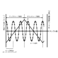
- FIG. 3 is a diagram for explaining an example of oversampling processing by the distance measuring device according to the embodiment.
- the frequency (chirp frequency) of the optical signal S1 which is the chirp signal described above, and the amplitude (signal level) of the beat signal input to the AD conversion unit 30 are shown on the same time axis. Note that in FIG. 3, the horizontal time axis is represented by the number of samples.
- the beat signal has a frequency equivalent to the frequency difference between the optical signals S1 and S2.
- the AD conversion unit 30 performs AD conversion processing on the beat signal during the chirp period (up-chirp period and down-chirp period in FIG. 3), which is the modulation period during which the laser light is frequency-modulated.
- the AD conversion unit 30 samples the beat signal at the frequency fLO1 of the local signal LO1 and outputs a digital signal for each sampling point.
- the AD conversion unit 30 samples the beat signal at M ⁇ M' (16 ⁇ 20) points per period of the beat signal and converts it into a digital signal (note that FIG. 3 only illustrates 16 sampling points per period). In this way, the AD conversion unit 30 oversamples the beat signal at frequency f LO1 , and outputs the beat signal converted into a digital signal for each sampling point to the sampling unit 35.
- the sampling unit 35 is a downsampling unit configured to be able to downsample an input signal.
- the sampling unit 35 receives a beat signal for each sampling point output from the AD conversion unit 30.
- the sampling unit 35 also receives a local signal LO2 having a frequency fLO2 lower than the frequency fLO1 from the oscillation unit 110 as a clock signal.
- the sampling unit 35 down-samples the beat signal at the frequency fLO2 of the local signal LO2 and outputs the down-sampled beat signal.
- the sampling unit 35 performs decimation (thinning-out) processing on the beat signal output from the AD conversion unit 30 and outputs a digital signal for each sampling point to the signal processing unit 40.
- the signal processing unit 40 is configured to be able to perform signal processing using the input signal.
- the signal processing unit 40 is made up of circuits that perform various types of signal processing on the beat signal.
- the signal processing unit 40 (signal processing circuit) is configured using multiple logic circuits, such as flip-flop circuits, adder circuits, and multiplier circuits.
- the signal processing unit 40 can perform various types of signal processing, such as phase detection processing and reference signal generation processing, as will be described later.
- the signal processing unit 40 includes a phase comparison unit 43.
- the phase comparison unit 43 is a phase comparator (PFD: Phase Frequency Detector) and is configured to be able to compare the phase (or frequency) of a signal. For example, a beat signal downsampled by the sampling unit 35 is input to the phase comparison unit 43.
- PFD Phase Frequency Detector
- the filter unit 50 is a low pass filter (LPF) and is configured to selectively pass signals in a predetermined frequency band.
- the signal processing unit 40 may be configured to include the filter unit 50.
- the signal processing unit 40 may be configured to include a memory unit 55 and an adder unit 61.
- the signal processing unit 40 compares the beat signal with a reference signal using a phase comparison unit 43 (phase comparison circuit), and generates and outputs a signal (correction signal S3) related to the amount of correction of the frequency of the optical signal (laser light).
- the signal processing unit 40 also generates a signal (correction signal S4) related to the amount of correction of the frequency of the optical signal at the above-mentioned sampling point, and stores it in the storage unit 55.
- the distance measuring device 1 can perform an OPLL (Optical Phase Locked Loop) operation using the correction signal S3, and can perform a pre-distortion operation using the correction signal S4 stored in the memory unit 55.
- OPLL Optical Phase Locked Loop
- the switch SW1 when performing an OPLL operation, the switch SW1 is turned on, and when performing a pre-distortion operation, the switch SW2 is turned on.
- the storage unit 55 includes a plurality of memories (memory cells).
- the storage unit 55 (storage circuit) is configured to be able to store the correction signal S4.
- the signal processing unit 40 can control the writing of data to the storage unit 55 and the reading of data from the storage unit 55 via the switch SW2 shown in FIG. 1.
- the storage unit 55 stores a plurality of correction signals S4 each corresponding to a plurality of sampling points.
- the control unit 90 shown in FIG. 1 is configured to supply a signal for controlling the light source unit 10 to the light source unit 10 and control the light source unit 10.
- the control unit 90 is configured to be able to control the frequency modulation of the optical signal of the light source unit 10.
- the control unit 90 generates a voltage signal V1 related to the amount of frequency modulation of the laser light of the light source unit 10 and outputs it to the light source unit 10.
- the control unit 90 can control the frequency, chirp rate, etc. of the laser light output by the light source unit 10 by controlling the voltage signal V1 supplied to the light source unit 10.
- the control unit 90 has a comparison unit 70, a setting unit 75, an addition unit 62, an integration unit 80, and a DA conversion unit 85.
- the comparison unit 70 is configured using a comparator circuit, for example a hysteresis comparator.
- An output signal of the integration unit 80 for example a signal corresponding to an integration value, is input to the comparison unit 70.
- the comparison unit 70 compares a signal indicating the integration value in the integration unit 80 with a signal indicating a reference value, and outputs an output signal that is the comparison result to the setting unit 75.
- the signal output from the comparison unit 70 is a signal related to the switching timing of the chirp signal, for example, a signal indicating the switching timing between up-chirp and down-chirp.
- the output signal from the comparison unit 70 can also be said to be a signal indicating the start or end of an up-chirp (or down-chirp).
- the setting unit 75 is configured to set an up-chirp (or down-chirp) in the light source unit 10.
- the setting unit 75 can also be called a chirp setting unit (or a ramp setting unit) configured to be able to set the chirp direction of the optical signal.
- the setting unit 75 outputs a signal having a signal value according to the comparison result by the comparison unit 70 to the addition unit 62 as a signal indicating an up-chirp (or down-chirp).
- the setting unit 75 outputs a signal indicating, for example, +1, and in the case of a down-chirp, outputs a signal indicating, for example, -1.
- the integrating unit 80 is configured to be capable of outputting a digital signal whose value changes at every predetermined time interval (period).
- a signal S11 is input to the integrating unit 80 via an adding unit 62 (adding circuit).
- the signal S11 has a value corresponding to, for example, the signal value (+1 or -1) of the output signal of the setting unit 75.
- the signal S12 output from the integrator 80 is, for example, a signal that changes in increments of a value according to the signal S11 input to the integrator 80 in synchronization with the edges of the local signal LO2.
- the integrator 80 outputs a signal S12 that increases monotonically in the case of an up-chirp, and outputs a signal S12 that decreases monotonically in the case of a down-chirp.
- the DA conversion unit 85 is configured to convert an input digital signal into an analog signal.
- the DA conversion unit 85 is a DAC (Digital to Analog Converter).
- the DA conversion unit 85 receives the signal S12 from the integrator unit 80 and is supplied with a local signal LO1 as a clock signal from the oscillator unit 110.
- the DA conversion unit 85 can convert the signal S12, which is a digital signal, into an analog signal in response to the local signal LO1.
- the DA conversion unit 85 converts the signal S12 into an analog signal in synchronization with the frequency f LO1 of the local signal LO1 to generate a voltage signal V1 and outputs it to the light source unit 10.
- the voltage signal V1 supplied to the light source unit 10 becomes a signal (ramp signal) that monotonically increases or decreases by a value corresponding to the signal S11 input to the integrating unit 80.
- the control unit 90 can control the frequency modulation of the laser light of the light source unit 10 by supplying the voltage signal V1 to the light source unit 10.
- the signal processing unit 40 of the distance measuring device 1 is configured to be able to generate a signal based on the difference between the beat signal and the reference signal as the correction signal S3.
- the signal processing unit 40 can detect the difference between the beat signal and the reference signal as a phase error by comparing the beat signal with the reference signal in the phase comparison unit 43, and generate a signal related to the magnitude of the phase error as the correction signal S3.
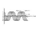
- Fig. 4 is a diagram showing an example of a beat signal and a reference signal of a distance measuring device according to an embodiment.
- the frequency of the optical signal S1 which is a chirp signal
- the amplitude (signal level) of the beat signal and the reference signal, and the phase error which is the difference between the beat signal and the reference signal
- the horizontal time axis is represented by the number of samplings.
- the reference signal shown by the dashed waveform represents an ideal signal of frequency f MZI assumed when the frequency modulation characteristic of the optical signal is linear.
- the signal processing unit 40 may calculate the difference between the beat signal and the reference signal as the phase error, as in the example shown in FIG. 4.
- the signal processing unit 40 generates a signal indicating the magnitude of the calculated phase error as a correction signal S3.
- the signal processing unit 40 outputs the generated correction signal S3 to the adder unit 61 via the filter unit 50 and switch SW1 shown in FIG. 1.
- the adder units 61 and 62 are each configured to be able to perform signal addition processing.
- the adder unit 61 can output the correction signal S3 from the signal processing unit 40 to the adder unit 62, and in the case of pre-distortion operation, the adder unit 61 can output the correction signal S4 from the storage unit 55 to the adder unit 62.
- the adder unit 61 can also output a signal obtained by adding the correction signal S3 and the correction signal S4 to the adder unit 62.
- the adder 62 adds the value of the output signal of the setting unit 75 (+1 or -1) to the value of the correction signal S3 to generate a signal S11, which is a digital signal indicating the added value.
- a signal S11 corrected according to the phase error between the beat signal and the reference signal is generated, and a signal S12 generated using the corrected signal S11 is output to the DA conversion unit 85.
- the DA conversion unit 85 converts the signal S12 adjusted according to the detected phase error into an analog signal, and outputs the generated voltage signal V1 to the light source unit 10.
- the light source unit 10 performs frequency modulation of the optical signal, which is laser light, according to the voltage signal V1.
- the distance measuring device 1 performs feedback so that the phase error is reduced and a stable state (locked state) is reached, and the OPLL operation can be performed.
- the voltage signal V1 changes according to the correction signal S3 so that the phase difference between the beat signal and the reference signal is reduced, and the amount of frequency modulation of the optical signal from the light source unit 10 is adjusted.
- the amount of frequency modulation of the optical signal can be corrected so that the frequency of the optical signal changes linearly and continuously. This makes it possible to prevent deterioration of the frequency modulation characteristics of the optical signal and improve distance measurement accuracy.
- the distance measuring device 1 performs OPLL operation using a beat signal oversampled at a frequency that is an integer multiple (multiple) of the frequency of the beat signal. This makes it possible to prevent the sampling points from decreasing and the tracking operation by the PLL from being incorrect. It becomes possible to suppress the deterioration of distance measuring performance.
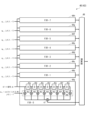
- FIG. 5 is a diagram for explaining an example of the configuration of a signal processing unit of a distance measuring device according to an embodiment.
- FIG. 6 is a diagram for explaining an example of signal processing by the signal processing unit of the distance measuring device.
- the signal processing unit 40 is configured to be capable of generating the above-mentioned reference signal based on the beat signal at each sampling point.
- the phase comparison unit 43 of the signal processing unit 40 has a plurality of FIR filters 44 (Finite Impulse Response) and an arithmetic unit 48, and is configured to generate a reference signal.
- Each of the FIR filters 44 has, for example, a plurality of flip-flops 45 (flip-flops 45a to 45g in FIG. 5), a plurality of multipliers 46 (multipliers 46a to 46h in FIG. 45), and an adder 47.
- a beat signal for each sampling point is input from the sampling unit 35 to each of the FIR filters 44a to 44h.
- a coefficient q i,j expressed by the following equation (1) is input to each of the FIR filters 44 as the coefficient of the FIR filter 44.
- i is the number of the FIR filter 44.
- j is the tap number index, which is the number of the multiplication unit 46 in the FIR filter 44.
- the coefficients expressed by the formula (1) are applied to the FIR filter 44 of the signal processing unit 40.
- the signal processing unit 40 can perform a convolution operation represented by the following equation (2) using the FIR filters 44a to 44h.
- the time k corresponds to the timing of the sampling point.
- the FIR filters 44a to 44h perform the arithmetic processing represented by the above-mentioned equation (2) using the flip-flop 45, the multiplier 46, the adder 47, etc., and output eight reference signals (reference signal (FIR-0) to reference signal (FIR-7)) as shown in FIG. 6.
- the multiple reference signals are signals indicating the cross-correlation values c i,j . It can also be said that the FIR filters 44a to 44h generate and output eight-phase reference signals having mutually different phases.
- the calculation unit 48 of the signal processing unit 40 compares the reference signal and beat signal output from each FIR filter 44, and determines (sets) the reference signal to be used in the calculation of the phase error described above. For example, the calculation unit 48 compares the peak value of the beat signal with the peak values of each of the eight output signals from the FIR filters 44a to 44h. Based on the comparison results of the peak values, the calculation unit 48 selects the reference signal that is closest to the beat signal from among the eight reference signals.
- the reference signal (reference signal (FIR-7)) generated by FIR filter 44h indicated by a dashed line is the reference signal closest to the beat signal and is selected as the reference signal to be used in calculating the phase error.
- the calculation unit 48 can detect the phase error as described above and generate the correction signal S3. In this way, the distance measuring device 1 according to this embodiment can obtain an appropriate reference signal for the beat signal to generate the correction signal S3 and control the amount of frequency modulation.
- the calculation unit 48 of the signal processing unit 40 may detect the zero crossing points, i.e., the points where the sign changes, and use the zero crossing points to estimate the peak position and generate the reference signal.
- l mod(n-M/4, M)
- mod(*, M) is a modulo function (operator) that indicates the positive remainder of division by the integer M.
- the reference waveform r l in these cases can be expressed by the following equation (3).
- phase error pk can be obtained by the following equation (4) when l ⁇ M/2, and by the following equation (5) when l>M/2.
- the reference signal obtained by the above-mentioned formula (2), (4), or (5) can be obtained using a correlation value that is the result of a convolution operation of beat signals from the past to the present stored in the FIR filter 44. This makes it possible to avoid the occurrence of pipeline delays. It is also possible to suppress the decrease in phase margin caused by an increase in the PLL loop delay.
- the signal processing unit 40 may have an offset correction unit 41 and a gain correction unit 42, as in the example shown in Fig. 1.
- the offset correction unit 41 is configured to be able to perform offset correction of the beat signal.
- the offset correction unit 41 is an offset cancellation circuit (OFC). If the beat signal is b_k, then the signal b'_k after the offset correction can be expressed, for example, by using the following equations (6) and (7).
- ⁇ is the update coefficient for the offset correction.
- the offset correction unit 41 can cancel the offset of the beat signal by performing the offset correction expressed by equations (6) and (7).
- the gain correction unit 42 is configured to be able to perform gain correction of the beat signal.
- the gain correction unit 42 is an AGC (Auto Gain Control) circuit.
- the gain correction unit 42 can perform gain correction expressed by the following equations (8), (9), and (10) on the signal b'_k output from the offset correction unit 41, and output a signal yk which is an output signal expressed by equation (11).
- ⁇ is an update coefficient for the gain correction.
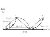
- FIG. 7 is a diagram for explaining an example of signal processing by the signal processing unit of the distance measuring device according to the embodiment.
- the signal processing unit 40 is configured to be able to generate a correction signal S4 relating to the amount of frequency correction for each sampling point.
- the signal processing unit 40 generates multiple correction signals S4 corresponding to the multiple sampling points respectively based on the beat signal for each sampling point, and stores them in the memory unit 55.
- the storage unit 55 has memories in a number corresponding to the number of sampling points.
- the sampling points are associated with the correction signal S4 indicating the correction value at the sampling point, and are stored in the memory corresponding to the sampling point.
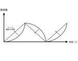
- the signal processing unit 40 repeats a comparison between the beat signal in one up-chirp period and the beat signal in the next up-chirp period for each chirp period to determine the chirp rate error and learn the chirp rate correction amount.
- the signal processing unit 40 also repeats a comparison between the beat signal in one down-chirp period and the beat signal in the next down-chirp period for each chirp period to learn the chirp rate correction amount.
- the signal processing unit 40 detects the phase error of the beat signal using the phase comparison unit 43, the calculation unit 48, etc., and stores the correction signal S4 in the memory unit 55.
- the correction signal S4 stored in the memory unit 55 is updated according to the phase error detected at each sampling point, making it possible to learn the amount of chirp rate correction.
- the distance measuring device 1 can perform pre-distortion operation using memory learning type ILC (Iterative Learning control).
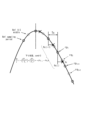
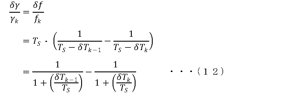
- the chirp rate error ⁇ / ⁇ k at time k can be expressed by the following equation (12): where Ts is the sampling period of the beat signal, and ⁇ Tk is the error of the sampling period at time k.
- equation (13) is obtained by a linear approximation of equation (12) and Taylor expansion.
- the chirp rate error ⁇ / ⁇ k can be expressed as the difference between the phase error pe_k at time k and the phase error pe_(k ⁇ 1) at the time (k ⁇ 1) one time earlier.
- the chirp rate error ⁇ / ⁇ k can be expressed by the difference between the frequency error and the phase error, etc.
- the signal processing unit 40 may generate a signal indicating the frequency error of the beat signal as the correction signal S4, and store the correction signal S4 generated for each sampling point in the storage unit 55.
- the signal processing unit 40 may generate a signal indicating the difference between the phase errors at each of two sampling points as the correction signal S4, and store the correction signal S4 generated for each sampling point in the storage unit 55.
- FIG. 8 is a diagram for explaining an example of a process for detecting a difference in phase error by the signal processing unit of the distance measuring device according to the embodiment.
- x points indicate beat signals at sampling points.
- a solid circle indicates a reference signal rp l expressed by the following equation (14), and a dotted circle indicates a reference signal rq l expressed by the following equation (15).
- the signal processing unit 40 can calculate the phase error pek on the time axis using the value of “cond” determined as described above and the following equations (16) to (19).
- the signal processing unit 40 calculates the phase error pek, and stores the correction signal S4 indicating the phase error pek in the storage unit 55.
- the signal processing unit 40 When the signal processing unit 40 performs a pre-distortion operation, it outputs the correction signal S4 stored in the memory unit 55 to the adder unit 62 via the switch SW2 and adder unit 61 shown in FIG. 1.
- the adder unit 62 adds the value of the output signal of the setting unit 75 (+1 or -1) to the value of the correction signal S4, and generates a signal S11, which is a digital signal indicating the added value.
- a signal S11 corrected according to the phase error of the beat signal is generated, and a signal S12 generated using the corrected signal S11 is output to the DA conversion unit 85.
- the DA conversion unit 85 converts the signal S12 adjusted according to the phase error into an analog signal and outputs the generated voltage signal V1 to the light source unit 10.
- the light source unit 10 performs frequency modulation of the optical signal, which is laser light, according to the voltage signal V1.
- the distance measuring device 1 can perform a pre-distortion operation to reduce the phase error.
- chirp linearization learning is performed by ILC using the signal processing unit 40 and the memory unit 55, etc., making it possible to appropriately correct the chirp rate.
- the voltage signal V1 changes according to the correction signal S4, and the amount of frequency modulation of the optical signal from the light source unit 10 is adjusted.
- the amount of frequency modulation of the optical signal can be corrected so that the frequency of the optical signal changes linearly and continuously. This makes it possible to prevent deterioration of the frequency modulation characteristics of the optical signal and improve distance measurement accuracy.
- the distance measuring device (distance measuring device 1) of this embodiment includes a light source unit (light source unit 10) capable of outputting a frequency-modulated optical signal, a detection unit (detection unit 20) capable of detecting a beat signal based on an optical signal and a delayed optical signal, an AD conversion unit (AD conversion unit 30) capable of sampling the beat signal at each sampling point and performing AD conversion, a signal processing unit (signal processing unit 40) capable of generating a first signal (e.g., correction signal S4) related to the amount of correction of the frequency of the optical signal based on the beat signal converted into a digital signal, a memory unit (memory unit 55) capable of storing a plurality of first signals respectively corresponding to a plurality of sampling points, and a control unit (control unit 90) capable of controlling the frequency modulation of the optical signal based on the first signal stored in the memory unit.
- a light source unit light source unit
- detection unit 20 capable of detecting a beat signal based on an optical signal and a delayed optical
- the distance measuring device 1 has a memory unit 55 capable of storing a plurality of correction signals S4 corresponding to a plurality of sampling points, and a control unit 90 capable of controlling the frequency modulation of the optical signal based on the correction signal S4. Therefore, in this embodiment, it is possible to prevent the frequency modulation characteristics of the optical signal from deteriorating. It is possible to realize a distance measuring device capable of improving the frequency modulation characteristics.
- the chirp rate can be appropriately corrected by pre-distortion using memory learning ILC, making it possible to improve distance measurement performance.
- the signal processing unit 40 is capable of generating a first signal (e.g., correction signal S3) based on the beat signal for each sampling point and the reference signal. Therefore, in this embodiment, the correction signal S3 can be used to perform OPLL operation, and the amount of frequency modulation of the optical signal can be appropriately corrected. It is possible to realize a distance measuring device capable of improving the frequency modulation characteristics. It is possible to prevent the frequency modulation characteristics of the optical signal from deteriorating, and to improve distance measuring performance.
- a first signal e.g., correction signal S3
- the correction signal S3 can be used to perform OPLL operation, and the amount of frequency modulation of the optical signal can be appropriately corrected. It is possible to realize a distance measuring device capable of improving the frequency modulation characteristics. It is possible to prevent the frequency modulation characteristics of the optical signal from deteriorating, and to improve distance measuring performance.
- the AD conversion unit 30 is capable of sampling the beat signal at a frequency that is an integer multiple of the frequency of the beat signal and performing AD conversion. This makes it possible to prevent a decrease in sampling points that would prevent the tracking operation by the PLL from being performed correctly.
- the distance measuring device 1 can suppress deterioration of the frequency modulation characteristics of the optical signal.
- the distance measuring device 1 may be configured so that the delay time ⁇ MZI of the interference unit 15 is ⁇ 3 ns and the chirp bandwidth ⁇ f of the optical signal by the light source unit 10 is ⁇ 1 GHz. In this case, it is also possible to prevent the tracking operation by the OPLL from being improperly performed and suppress a deterioration in distance measuring performance.
- the distance measuring device 1 may be configured to be capable of performing only one of the above-mentioned OPLL operation and pre-distortion operation.
- the distance measuring device 1 may set both switches SW1 and SW2 to an on state and perform both the OPLL operation and the pre-distortion operation simultaneously (in parallel).
- the distance measuring device 1 may add the correction signal S3 and the correction signal S4 by the adder 61, and correct the frequency modulation amount based on the added correction signal.
- the technology disclosed herein can be applied to various circuits and devices.
- the distance measuring device 1, the signal processing unit 40, and the like described above can be used in various devices and circuits that perform distance measurement.
- the technology disclosed herein can be applied to various products, for example, as various distance measuring devices, photodetectors capable of detecting incident light, signal processing devices, and the like.
- the optical detection device includes a detection unit (detection unit 20) capable of detecting a beat signal based on a frequency-modulated optical signal and a delayed optical signal output from a light source unit (light source unit 10), an AD conversion unit (AD conversion unit 30) capable of sampling the beat signal at each sampling point and performing AD conversion, a signal processing unit (signal processing unit 40) capable of generating a first signal (e.g., correction signal S4) related to the amount of correction of the frequency of the optical signal based on the beat signal converted into a digital signal, a memory unit (memory unit 55) capable of storing a plurality of first signals corresponding to a plurality of sampling points, and a control unit (control unit 90) capable of controlling the frequency modulation of the optical signal based on the first signal stored in the memory unit.
- a detection unit detection unit 20
- AD conversion unit 30 capable of sampling the beat signal at each sampling point and performing AD conversion
- signal processing unit 40 capable of generating a first signal (e.g., correction signal S
- the signal processing device of one embodiment of the present disclosure includes a detection unit (detection unit 20) capable of detecting a beat signal based on a frequency-modulated optical signal and a delayed optical signal output from a light source unit (light source unit 10), an AD conversion unit (AD conversion unit 30) capable of sampling the beat signal at each sampling point and performing AD conversion, a signal processing unit (signal processing unit 40) capable of generating a first signal (e.g., correction signal S4) related to the correction amount of the frequency of the optical signal based on the beat signal converted into a digital signal, a memory unit (memory unit 55) capable of storing a plurality of first signals corresponding to a plurality of sampling points, and a control unit (control unit 90) capable of outputting a signal (e.g., voltage signal V1) that controls the frequency modulation of the optical signal based on the first signal stored in the memory unit. Therefore, it is possible to suppress deterioration of the frequency modulation characteristics of the optical signal. It is possible to realize a signal
- the present disclosure may have the following configurations.
- a light source unit capable of outputting a frequency modulated optical signal; a detector capable of detecting a beat signal based on the optical signal and a delayed optical signal; an AD conversion unit capable of sampling the beat signal at each sampling point and performing AD conversion; a signal processing unit capable of generating a first signal related to a correction amount of the frequency of the optical signal based on the beat signal converted into a digital signal; a storage unit capable of storing a plurality of the first signals respectively corresponding to the plurality of sampling points; and a control unit capable of controlling frequency modulation of the optical signal based on the first signal stored in the memory unit.
- the signal processing unit is capable of generating a plurality of the first signals respectively corresponding to a plurality of the sampling points based on the beat signal for each sampling point converted into a digital signal.
- the signal processing unit is capable of generating the first signal based on a difference between the beat signal in a first modulation period and the beat signal in a second modulation period.
- the signal processing unit is capable of generating, as the first signal, a signal related to a frequency error of the beat signal.
- the distance measuring device (5) The distance measuring device according to any one of (1) to (4), wherein the signal processing unit is capable of generating, as the first signal, a signal related to a difference in phase error of the beat signals.
- the storage unit has a number of memories corresponding to the number of the plurality of sampling points and is capable of storing the plurality of first signals corresponding to the plurality of sampling points, respectively.
- the AD conversion unit is capable of sampling the beat signal at a frequency that is an integer multiple of a frequency of the beat signal and performing AD conversion.
- the distance measuring device according to any one of (8) to (10), wherein the signal processing unit is capable of comparing the beat signal with a plurality of reference signals and generating the first signal relating to a difference between the beat signal and the reference signal selected based on a comparison result.
- the signal processing unit is capable of comparing the beat signal with a plurality of reference signals and generating the first signal relating to a difference between the beat signal and the reference signal selected based on a comparison result.
- the distance measuring device according to any one of (1) to (11), further comprising a sampling unit capable of down-sampling the beat signal output from the AD conversion unit.
- the signal processing unit is capable of generating the first signal based on the beat signal downsampled by the sampling unit.
- the distance measuring device according to any one of (1) to (13), further comprising an offset correction unit capable of performing offset correction of the beat signal.
- the distance measuring device 15) The distance measuring device according to (14), wherein the signal processing unit is capable of generating the first signal based on the beat signal corrected by the offset correction unit. (16) The distance measuring device according to any one of (1) to (15), further comprising a gain correction unit capable of performing gain correction of the beat signal. (17) The distance measuring device according to (16), wherein the signal processing unit is capable of generating the first signal based on the beat signal corrected by the gain correction unit. (18) The distance measuring device according to any one of (1) to (17), wherein the distance measuring device is an FMCW type distance measuring device.
- a detector capable of detecting a beat signal based on a frequency-modulated optical signal output from a light source and a delayed optical signal; an AD conversion unit capable of sampling the beat signal at each sampling point and performing AD conversion; a signal processing unit capable of generating a first signal related to a correction amount of the frequency of the optical signal based on the beat signal converted into a digital signal; a storage unit capable of storing a plurality of the first signals respectively corresponding to the plurality of sampling points; and a control unit capable of controlling frequency modulation of the optical signal based on the first signal stored in the memory unit.
- a detector capable of detecting a beat signal based on a frequency-modulated optical signal output from a light source and a delayed optical signal; an AD conversion unit capable of sampling the beat signal at each sampling point and performing AD conversion; a signal processing unit capable of generating a first signal related to a correction amount of the frequency of the optical signal based on the beat signal converted into a digital signal; a storage unit capable of storing a plurality of the first signals respectively corresponding to the plurality of sampling points; a control unit capable of outputting a signal for controlling frequency modulation of the optical signal based on the first signal stored in the storage unit.
Landscapes
- Engineering & Computer Science (AREA)
- Physics & Mathematics (AREA)
- Computer Networks & Wireless Communication (AREA)
- General Physics & Mathematics (AREA)
- Radar, Positioning & Navigation (AREA)
- Remote Sensing (AREA)
- Electromagnetism (AREA)
- Optical Radar Systems And Details Thereof (AREA)
Abstract
本開示の一実施形態の測距装置は、周波数変調された光信号を出力可能な光源部(10)と、前記光信号(S1)と遅延された前記光信号(S2)とに基づくビート信号を検出可能な検出部(20)と、前記ビート信号をサンプリング点毎にサンプリングし、AD変換を実行可能なAD変換部(30)と、デジタル信号に変換された前記ビート信号に基づいて、前記光信号の周波数の補正量に関する第1信号(S4)を生成可能な信号処理部(40)と、複数の前記サンプリング点にそれぞれ対応する複数の前記第1信号(S4)を記憶可能な記憶部(55)と、前記記憶部に記憶された前記第1信号(S4)に基づいて、前記光信号の周波数変調を制御可能な制御部(90)とを備える。
Description
本開示は、測距装置、光検出装置、および信号処理装置に関する。
送信信号の周波数変調特性の非線形歪みを補正するFM-CW方式のレーザレーダ装置が提案されている(特許文献1)。
測距装置では、周波数変調特性を向上させることが望ましい。
周波数変調特性を向上可能な測距装置を提供することが望まれる。
本開示の一実施形態の測距装置は、周波数変調された光信号を出力可能な光源部と、光信号と遅延された光信号とに基づくビート信号を検出可能な検出部と、ビート信号をサンプリング点毎にサンプリングし、AD変換を実行可能なAD変換部と、デジタル信号に変換されたビート信号に基づいて、光信号の周波数の補正量に関する第1信号を生成可能な信号処理部と、複数のサンプリング点にそれぞれ対応する複数の第1信号を記憶可能な記憶部と、記憶部に記憶された第1信号に基づいて、光信号の周波数変調を制御可能な制御部とを備える。
本開示の一実施形態の光検出装置は、光源部から出力される周波数変調された光信号と遅延された光信号とに基づくビート信号を検出可能な検出部と、ビート信号をサンプリング点毎にサンプリングし、AD変換を実行可能なAD変換部と、デジタル信号に変換されたビート信号に基づいて、光信号の周波数の補正量に関する第1信号を生成可能な信号処理部と、複数のサンプリング点にそれぞれ対応する複数の第1信号を記憶可能な記憶部と、記憶部に記憶された第1信号に基づいて、光信号の周波数変調を制御可能な制御部とを備える。
本開示の一実施形態の信号処理装置は、光源部から出力される周波数変調された光信号と遅延された光信号とに基づくビート信号を検出可能な検出部と、ビート信号をサンプリング点毎にサンプリングし、AD変換を実行可能なAD変換部と、デジタル信号に変換されたビート信号に基づいて、光信号の周波数の補正量に関する第1信号を生成可能な信号処理部と、複数のサンプリング点にそれぞれ対応する複数の第1信号を記憶可能な記憶部と、記憶部に記憶された第1信号に基づいて、光信号の周波数変調を制御する信号を出力可能な制御部とを備える。
本開示の一実施形態の光検出装置は、光源部から出力される周波数変調された光信号と遅延された光信号とに基づくビート信号を検出可能な検出部と、ビート信号をサンプリング点毎にサンプリングし、AD変換を実行可能なAD変換部と、デジタル信号に変換されたビート信号に基づいて、光信号の周波数の補正量に関する第1信号を生成可能な信号処理部と、複数のサンプリング点にそれぞれ対応する複数の第1信号を記憶可能な記憶部と、記憶部に記憶された第1信号に基づいて、光信号の周波数変調を制御可能な制御部とを備える。
本開示の一実施形態の信号処理装置は、光源部から出力される周波数変調された光信号と遅延された光信号とに基づくビート信号を検出可能な検出部と、ビート信号をサンプリング点毎にサンプリングし、AD変換を実行可能なAD変換部と、デジタル信号に変換されたビート信号に基づいて、光信号の周波数の補正量に関する第1信号を生成可能な信号処理部と、複数のサンプリング点にそれぞれ対応する複数の第1信号を記憶可能な記憶部と、記憶部に記憶された第1信号に基づいて、光信号の周波数変調を制御する信号を出力可能な制御部とを備える。
以下、本開示の実施の形態について、図面を参照して詳細に説明する。なお、説明は以下の順序で行う。
1.実施の形態
2.変形例
3.適用例
1.実施の形態
2.変形例
3.適用例
<1.実施の形態>
図1は、本開示の実施の形態に係る測距装置の概略構成の一例を示す図である。測距装置1は、測距を実行可能な装置である。測距装置1は、例えば、FMCW(Frequency Modulated Continuous Wave)方式の測距装置であり、FMCW―LiDAR(Light Detection and Ranging)として適用され得る。
図1は、本開示の実施の形態に係る測距装置の概略構成の一例を示す図である。測距装置1は、測距を実行可能な装置である。測距装置1は、例えば、FMCW(Frequency Modulated Continuous Wave)方式の測距装置であり、FMCW―LiDAR(Light Detection and Ranging)として適用され得る。
なお、ライダー装置である測距装置1は、レーザレーダ装置ともいえる。測距装置1は、周波数変調された変調光となる光信号の送受信を行い、計測対象物までの距離、計測対象物の速度等を計測し得る。測距装置1は、例えば、シリコン基板、SOI(Silicon On Insulator)基板等を用い、Silicon Photonics(SiPh)技術を利用して製造され得る。
測距装置1は、光源部10によって計測対象に周波数変調されたレーザ光を照射し、計測対象で反射され遅延されたレーザ光を受光し得る。測距装置1では、例えば、光源部10の出力光(照射光)から分岐(分離)した参照光と、計測対象で反射された反射光とを干渉させて得られる光信号が検出部20に入力され、参照光の周波数と反射光の周波数の差に応じた周波数を有するビート信号が検出される。計測対象からの反射光を受光して生成されるビート信号は、計測対象までの距離に応じた信号となる。
測距装置1は、ビート信号の周波数(ビート周波数)を解析することにより、測距装置1と計測対象物との距離を算出し得る。また、測距装置1は、光のドップラーシフトを利用して計測対象物の速度(相対速度)を算出し得る。一例として、測距装置1は、レーザ光の周波数を時間経過と共に増加させた場合、即ちアップチャープの場合のビート周波数と、レーザ光の周波数を時間経過と共に減少させた場合、即ちダウンチャープの場合のビート周波数とに基づき、計測対象物の速度を演算する。
例えば、測距装置1は、三角波状に周波数変調された光信号となるレーザ光を出射し、連続するアップチャープ及びダウンチャープの各々の場合のビート信号のビート周波数を用いて、計測対象物の速度、計測対象物までの距離等を算出し得る。測距装置1は、このように、時間経過と共に周波数が連続して変化する信号(チャープ信号)を生成可能に構成される。測距装置1は、信号処理装置であり、チャープ発生装置(又はチャープ信号生成装置)ともいえる。
また、本実施の形態に係る測距装置1では、後述するが、干渉部15及び検出部20等により所定周波数を有するビート信号が生成され、光信号(レーザ光)の周波数変調量の補正に用いられる。このビート信号は、補正用のビート信号ともいえる。
測距装置1は、図1に示すように、第1回路ブロック101と、第2回路ブロック102とを備える。第1回路ブロック101は、主にアナログ回路を用いて構成され、アナログ信号処理を実行可能に構成される。第1回路ブロック101は、アナログブロックともいえる。第2回路ブロック102は、主にデジタル回路を用いて構成され、デジタル信号処理を実行可能に構成される。第2回路ブロック102は、デジタルブロックともいえる。
第1回路ブロック101は、光源部10と、干渉部15と、検出部20とを有する。光源部10は、周波数変調された光信号を出力可能に構成される。光源部10は、例えば可変レーザ光源を有し、計測対象に対して光を照射可能に構成される。光源部10は、周波数変調されたレーザ光を発生し、レーザ光を出射し得る。光源部10は、光信号を送信可能に構成された送信部ともいえる。
検出部20は、受光部21を有し、入射する光を検出可能に構成される。受光部21(受光素子)は、例えば、フォトダイオードPDを用いて構成される。受光部21は、光を受光して光電変換により電荷を生じ、電流を出力し得る。例えば、光源部10からのレーザ光と遅延されたレーザ光とがミキシング(混合)された光信号の受信に応じて、受光部21を流れる光電流に応じた信号が生成され、ビート信号として出力される。検出部20は、光信号を受信可能に構成された受信部であり、光信号を電気信号に変換するように構成される。
図1に示す例では、検出部20は、アンプ部22と、フィルタ部23とを有する。アンプ部22(アンプ回路)は、例えば、トランスインピーダンスアンプ(TIA:Transimpedance Amplifier)を含み、電流信号を電圧信号に変換するように構成される。アンプ部22は、受光部21で検出された電流信号を電圧信号に変換し、電圧信号であるビート信号をフィルタ部23へ出力し得る。
フィルタ部23は、所定の周波数帯域の信号を選択的に通過させるように構成される。フィルタ部23は、例えば、アンチエイリアスフィルタ(AAF:Anti-Aliasing Filter)を用いて構成される。フィルタ部23は、アンプ部22から入力されるビート信号のうち、不要な帯域の信号成分を除去する処理を行うように構成される。
干渉部15は、光源部10からのレーザ光と遅延させたレーザ光とを干渉させ、干渉した光(干渉光)を出力可能に構成される。干渉部15は、複数の光信号を合波(結合)した光信号を、検出部20の受光部21へ出力し得る。干渉部15は、例えば、マッハツェンダー干渉計(MZI:Mach-Zehnder Interferometer)により構成される。
図2は、実施の形態に係る測距装置により生成される信号の一例を示す図である。図2において、縦軸はチャープ信号の周波数を示し、横軸は時刻を示している。図2は、光源部10からのレーザ光である光信号S1と、このレーザ光を遅延時間(遅延量)であるτMZI遅延させたレーザ光である光信号S2とを表している。干渉部15は、チャープ信号である光信号S1及び光信号S2をミキシングさせて生じる干渉光を、検出部20の受光部21へ出力する。
検出部20は、受光部21によって干渉部15からの干渉光を受光し、上述のようにビート信号を生成して出力し得る。干渉部15からの干渉光を受光して生成されるビート信号は、光信号S1の周波数と光信号S2の周波数との差に応じた周波数を有する信号となる。例えば、レーザ光のチャープレートをγ(単位は、例えばGHz/us)とすると、遅延時間τMZIを用いて、ビート信号の周波数fMZIは、γ×τMZIとなる。測距装置1では、この周波数fMZIのビート信号を用いて、光信号の周波数変調量の補正を行うことが可能となる。
第2回路ブロック102は、AD変換部30と、サンプリング部35と、信号処理部40と、フィルタ部50と、記憶部55と、スイッチSW1,SW2と、制御部90とを含んで構成される。また、測距装置1は、図1に示すように、発振部110を有する。発振部110(発振回路)は、例えば、局部発振器(Local Oscillator)である。発振部110は、周波数fLO1を有する信号(ローカル信号LO1と称する)を出力可能に構成される。
発振部110は、ビート信号の周波数よりも高い周波数、例えばビート信号の周波数の整数倍(逓倍)の周波数を有するローカル信号LO1を生成し、AD変換部30及びDA変換部85等へ出力し得る。ローカル信号LO1の周波数fLO1は、例えば、M×M’×γ×τMZIとなる。一例として、M=16、M’=20である。この場合、周波数fLO1は、ビート信号の周波数fMZI(=γ×τMZI)を、16×20倍した周波数となる。
また、発振部110は、周波数fLO1(=M×M’×γ×τMZI)よりも低い周波数fLO2(=M×γ×τMZI)を有する信号(ローカル信号LO2と称する)を出力可能に構成される。周波数fLO2は、周波数fLO1を1/M’(=1/20)した周波数となる。
図1に示す例では、発振部110は、周波数fLO1を有するローカル信号LO1を、AD変換部30、DA変換部85等に供給する。また、発振部110は、周波数fLO2を有するローカル信号LO2を、サンプリング部35、信号処理部40、積分部80等に供給する。AD変換部30によるAD変換処理及びDA変換部85によるDA変換処理は、ローカル信号LO1に同期して実行可能であり、信号処理部40及び積分部80等におけるデジタル信号処理は、ローカル信号LO2に同期して実行可能である。
AD変換部30は、入力されるアナログ信号をデジタル信号に変換するように構成される。AD変換部30は、ADC(Analog to Digital Converter)である。AD変換部30には、検出部20からビート信号が入力され、発振部110からクロック信号としてローカル信号LO1が供給される。AD変換部30は、ローカル信号LO1に応じてビート信号をサンプリングし、アナログ信号であるビート信号をデジタル信号に変換し得る。
図3は、実施の形態に係る測距装置によるオーバーサンプリング処理の一例を説明するための図である。図3では、同一の時間軸上に、上述したチャープ信号である光信号S1の周波数(チャープ周波数)と、AD変換部30に入力されるビート信号の振幅(信号レベル)とを図示している。なお、図3では、横軸の時間軸を、サンプリング数により表している。
図3に示す例のように、ビート信号は、光信号S1と光信号S2の周波数差に相当する周波数を有する。AD変換部30は、レーザ光が周波数変調される変調期間であるチャープ期間(図3では、アップチャープ期間、ダウンチャープ期間)において、ビート信号に対してAD変換処理を行う。
AD変換部30は、ローカル信号LO1の周波数fLO1でビート信号をサンプリングし、サンプリング点毎のデジタル信号を出力する。この場合、AD変換部30は、サンプリング周波数となる周波数fLO1(=M×M’×γ×τMZI)のローカル信号LO1に同期して、ビート信号をサンプリングする。
AD変換部30は、ビート信号の1周期毎にM×M’(16×20)点ずつ、ビート信号をサンプリングしてデジタル信号に変換する(なお、図3では、1周期のうち16点のサンプリング点のみ図示している。)。このように、AD変換部30は、周波数fLO1でビート信号のオーバーサンプリングを行い、デジタル信号に変換されたサンプリング点毎のビート信号をサンプリング部35へ出力する。
サンプリング部35は、ダウンサンプリング部であり、入力される信号をダウンサンプリング可能に構成される。サンプリング部35には、AD変換部30から出力されるサンプリング点毎のビート信号が入力される。また、サンプリング部35には、発振部110からクロック信号として、周波数fLO1よりも低い周波数fLO2を有するローカル信号LO2が供給される。
サンプリング部35は、ローカル信号LO2の周波数fLO2でビート信号をダウンサンプリングし、ダウンサンプリングされたビート信号を出力する。この場合、例えば、サンプリング部35は、AD変換部30から出力されるビート信号に対してデシメーション(間引き)処理を行い、サンプリング点毎のデジタル信号を信号処理部40へ出力する。
信号処理部40は、入力される信号を用いて信号処理を実行可能に構成される。信号処理部40は、ビート信号に対して各種の信号処理を施す回路により構成される。信号処理部40(信号処理回路)は、例えば、フリップフロップ回路、加算回路、乗算回路など、複数のロジック回路を用いて構成される。信号処理部40は、後述するが、例えば、位相検出処理、参照信号の生成処理等、各種の信号処理を行い得る。
図1に示す例では、信号処理部40は、位相比較部43を含んで構成される。位相比較部43は、位相比較器(PFD:Phase Frequency Detector)であり、信号の位相(又は周波数)を比較可能に構成される。位相比較部43には、例えば、サンプリング部35によりダウンサンプリングされたビート信号が入力される。
フィルタ部50は、ローパスフィルタ(LPF:Low Pass Filter)であり、所定の周波数帯域の信号を選択的に通過させるように構成される。なお、信号処理部40は、フィルタ部50を含んで構成されてもよい。また、信号処理部40は、記憶部55及び加算部61を含んで構成されてもよい。
信号処理部40は、例えば、位相比較部43(位相比較回路)によりビート信号と参照信号とを比較し、光信号(レーザ光)の周波数の補正量に関する信号(補正用信号S3)を生成して出力する。また、信号処理部40は、上述したサンプリング点における光信号の周波数の補正量に関する信号(補正用信号S4)を生成して、記憶部55に記憶させる。
測距装置1は、後述するが、補正用信号S3を用いてOPLL(Optical Phase Locked Loop)動作を行い、記憶部55に記憶された補正用信号S4を用いてpre-distortion動作を行い得る。測距装置1では、例えば、OPLL動作を行う場合はスイッチSW1がオン状態となり、pre-distortion動作を行う場合はスイッチSW2がオン状態とされる。
記憶部55は、複数のメモリ(メモリセル)を含んで構成される。記憶部55(記憶回路)は、補正用信号S4を記憶可能に構成される。信号処理部40は、図1に示すスイッチSW2を介して、記憶部55へのデータの書き込み、及び記憶部55からのデータの読み込みを制御し得る。記憶部55には、複数のサンプリング点にそれぞれ対応する複数の補正用信号S4が記憶される。
図1に示す制御部90は、光源部10を制御する信号を光源部10へ供給し、光源部10を制御するように構成される。制御部90は、光源部10の光信号の周波数変調を制御可能に構成される。例えば、制御部90は、光源部10のレーザ光の周波数変調量に関する電圧信号V1を生成し、光源部10へ出力する。制御部90は、光源部10に供給される電圧信号V1を制御することで、光源部10が出力するレーザ光の周波数、チャープレート等を制御し得る。
図1に示す例では、制御部90は、比較部70と、設定部75と、加算部62と、積分部80と、DA変換部85とを有する。比較部70は、コンパレータ回路、例えばヒステリシスコンパレータを用いて構成される。比較部70には、積分部80の出力信号、例えば積分値に応じた信号が入力される。比較部70は、一例として、積分部80における積分値を示す信号と、基準値を示す信号とを比較し、比較結果である出力信号を設定部75へ出力する。
比較部70から出力される信号は、チャープ信号の切り替えタイミングに関する信号であり、例えばアップチャープ及びダウンチャープの切り替えタイミングを示す信号となる。比較部70の出力信号は、アップチャープ(又はダウンチャープ)の開始又は終了を指示する信号ともいえる。
設定部75は、光源部10におけるアップチャープ(又はダウンチャープ)を設定するように構成される。設定部75は、光信号のチャープ方向を設定可能に構成されたチャープ設定部(又はランプ設定部)ともいえる。設定部75は、例えば、比較部70の出力信号に基づき、アップチャープ(又はダウンチャープ)を指示する信号として、比較部70による比較結果に応じた信号値を有する信号を加算部62へ出力する。設定部75は、アップチャープの場合、例えば+1を示す信号を出力し、ダウンチャープの場合、例えば-1を示す信号を出力する。
積分部80は、所定の時間間隔(周期)毎に値が変化するデジタル信号を出力可能に構成される。積分部80には、加算部62(加算回路)を介して信号S11が入力される。信号S11は、例えば、設定部75の出力信号の信号値(+1又は-1)に応じた値となる。積分部80(積分回路)は、例えば、周波数fLO2(=M×γ×τMZI)を有するローカル信号LO2に同期して、時間経過と共に値が増加する信号、又は時間経過と共に値が減少する信号S12を生成し、DA変換部85へ出力し得る。
積分部80から出力される信号S12は、例えば、ローカル信号LO2のエッジに同期して、積分部80に入力される信号S11に応じた値ずつ変化する信号となる。例えば、積分部80は、アップチャープの場合に単調増加する信号S12を出力し、ダウンチャープの場合に単調減少する信号S12を出力する。
DA変換部85は、入力されるデジタル信号をアナログ信号に変換するように構成される。DA変換部85は、DAC(Digital to Analog Converter)である。DA変換部85には、積分部80から信号S12が入力され、発振部110からクロック信号としてローカル信号LO1が供給される。DA変換部85は、ローカル信号LO1に応じて、デジタル信号である信号S12をアナログ信号に変換し得る。
DA変換部85は、ローカル信号LO1の周波数fLO1に同期して信号S12をアナログ信号に変換することで電圧信号V1を生成し、光源部10へ出力する。光源部10に供給される電圧信号V1は、積分部80に入力される信号S11に対応する値ずつ単調増加又は単調減少する信号(ランプ信号)となる。制御部90は、電圧信号V1を光源部10に供給することにより、光源部10のレーザ光の周波数変調を制御し得る。
測距装置1の信号処理部40は、ビート信号と基準信号との差分に基づく信号を、補正用信号S3として生成可能に構成される。信号処理部40は、例えば、位相比較部43におけるビート信号と基準信号との比較によって、ビート信号と基準信号との差分を位相誤差として検出し、位相誤差の大きさに関する信号を補正用信号S3として生成し得る。
図4は、実施の形態に係る測距装置のビート信号と参照信号の一例を示す図である。図4では、同一の時間軸上に、チャープ信号である光信号S1の周波数と、ビート信号及び参照信号の振幅(信号レベル)と、ビート信号及び参照信号の差である位相誤差を示している。なお、図4では、横軸の時間軸を、サンプリング数により表している。破線の波形で示す参照信号は、光信号の周波数変調特性が線形である場合に想定される周波数fMZIの理想信号を表している。
信号処理部40は、図4に示す例のように、ビート信号と参照信号との差分を位相誤差として算出し得る。信号処理部40は、算出した位相誤差の大きさを示す信号を、補正用信号S3として生成する。信号処理部40は、生成した補正用信号S3を、図1に示すフィルタ部50及びスイッチSW1を介して、加算部61へ出力する。
加算部61及び加算部62は、それぞれ、信号の加算処理を実行可能に構成される。加算部61は、例えば、OPLL動作の場合、信号処理部40からの補正用信号S3を加算部62へ出力し、pre-distortion動作の場合、記憶部55からの補正用信号S4を加算部62へ出力し得る。なお、加算部61は、補正用信号S3と補正用信号S4とを加算した信号を、加算部62へ出力することも可能である。
加算部62は、設定部75の出力信号の値(+1又は-1)と補正用信号S3の値とを加算し、加算値を示すデジタル信号である信号S11を生成する。補正用信号S3が加算されることで、ビート信号及び参照信号間の位相誤差に応じて補正された信号S11が生成され、補正された信号S11を用いて生成される信号S12がDA変換部85へ出力される。DA変換部85は、検出された位相誤差に応じて調整された信号S12をアナログ信号に変換し、生成した電圧信号V1を光源部10へ出力する。光源部10は、電圧信号V1に応じてレーザ光である光信号の周波数変調を行う。
こうして、測距装置1は、位相誤差が小さくなって安定した状態(ロック状態)となるようにフィードバックを行い、OPLL動作を行うことができる。測距装置1では、ビート信号と参照信号との位相差が小さくなるように、補正用信号S3に応じて電圧信号V1が変化し、光源部10の光信号の周波数変調量が調整される。光信号の周波数が直線的に連続して変化するように、光信号の周波数変調量を補正することができる。これにより、光信号の周波数変調特性が悪化することを抑制し、測距精度を向上させることが可能となる。
ビート信号の周波数fMZIの大きさによっては、ビート信号のサンプリング点が減少し、PLLによる追従動作が困難となるおそれがある。特に、SiPh技術を利用して製造された測距装置1を車載用の測距装置に適用した場合に、安定したPLL動作を実現することが困難となるおそれがある。そこで、本実施の形態に係る測距装置1は、ビート信号の周波数の整数倍(逓倍)の周波数でオーバーサンプリングしたビート信号を用いて、OPLL動作を行う。このため、サンプリング点が減少してPLLによる追従動作が正しく行われなくなることを防ぐことができる。測距性能の低下を抑制することが可能となる。
図5は、実施の形態に係る測距装置の信号処理部の構成例を説明するための図である。図6は、測距装置の信号処理部による信号処理の一例を説明するため図である。信号処理部40は、サンプリング点毎のビート信号に基づき、上述した参照信号を生成可能に構成される。
信号処理部40の位相比較部43は、複数のFIRフィルタ44(Finite Impulse Response)及び演算部48を有し、参照信号を生成するように構成される。信号処理部40は、例えば、M/2相のFIR構造を有する。図5に示す例では、信号処理部40は、M(=16)/2=8個のFIRフィルタ44a~FIRフィルタ44h(FIR-0~FIR-7)を有する。8個のFIRフィルタ44a~44hは、並列に配置される。
各FIRフィルタ44(FIRフィルタ44a~44h)は、それぞれ、例えば、複数のフリップフロップ45(図5ではフリップフロップ45a~45g)と、複数の乗算部46(図45は乗算部46a~46h)と、加算部47とを有する。FIRフィルタ44a~44hには、それぞれ、例えば、サンプリング部35からサンプリング点毎のビート信号が入力される。また、図5に示すように、各FIRフィルタ44には、次式(1)で表される係数qi,jが、FIRフィルタ44の係数として入力される。

なお、式(1)において、iは、FIRフィルタ44の番号である。図5に示す例では、i=0~7は、それぞれ、FIRフィルタ44a~44h(FIR-0~FIR-7)に対応する。また、jは、タップ番号インデックスであり、FIRフィルタ44内の乗算部46の番号である。図5に示す例では、j=0~7は、それぞれ、乗算部46a~46hに対応する。
信号処理部40のFIRフィルタ44には、上述したように、式(1)で表される係数が与えられる。例えば、図5に示すFIRフィルタ44aの乗算部46aには、フィルタ係数として、式(1)においてi=0、j=0とした場合の係数q0,0が設定される。また、例えば、FIRフィルタ44aの乗算部46bには、フィルタ係数として、式(1)においてi=0、j=1とした場合の係数q0,1が設定される。
時刻kにおけるビート信号をykとすると、FIRフィルタ44a~44hにビート信号ykが入力される場合、信号処理部40は、FIRフィルタ44a~44hによって、次式(2)で表される畳み込み演算を行い得る。時刻kは、サンプリング点のタイミングに対応する。

図6では、ビート信号ykの波形と、FIRフィルタ44a~44hから出力される信号の波形とを図示している。FIRフィルタ44a~44hは、フリップフロップ45、乗算部46、及び加算部47等によって上述した式(2)で表される演算処理を行い、図6に示すような8つの参照信号(参照信号(FIR-0)~参照信号(FIR-7))を出力する。複数の参照信号は、相互相関値ci,jを示す信号となる。FIRフィルタ44a~44hは、互いに異なる位相を有する8相の参照信号を生成して出力するともいえる。
信号処理部40の演算部48は、各FIRフィルタ44から出力される参照信号とビート信号とを比較し、上述した位相誤差の演算に用いる参照信号を決定(設定)する。例えば、演算部48は、ビート信号のピーク値と、FIRフィルタ44a~44hからの8つの出力信号の各々のピーク値とを比較する。演算部48は、ピーク値の比較結果に基づき、8つの参照信号のうちビート信号に最も近い参照信号を選択する。
図6に示す例では、8つの参照信号のうち、破線で示したFIRフィルタ44hで生成された参照信号(参照信号(FIR-7))が、ビート信号に最も近い参照信号となり、位相誤差の演算に用いる参照信号として選択される。演算部48は、選択した参照信号とビート信号を用いて、上述のように位相誤差を検出し、補正用信号S3を生成し得る。このように、本実施の形態に係る測距装置1では、ビート信号に対して適切な参照信号を取得して補正用信号S3を生成し、周波数変調量の制御を行うことが可能となる。
なお、相互相関値ci,jのピーク値が時間的に変動した場合、ピーク検出を行うことが困難となるおそれがある。そこで、信号処理部40の演算部48は、ゼロクロス点、即ち符号が変化する点を検出して、ゼロクロス点を用いてピーク位置を推定し、参照信号を生成するようにしてもよい。
例えば、ある時刻kに参照信号の各サンプリング点の値のうちn番目の自己相関値がNegative Edge(正(+1)から負(―1)への遷移)であった場合には、ピーク位置として、l=mod(n―M/4,M)を用いて、n番目のM/4(=4)クロック前の位置が求められる。なお、lは、相関位相であり、mod(*,M)は、整数Mによる除算の正の余りを示すModulo関数(演算子)である。
また、ある時刻kに参照信号の各サンプリング点の値のうちn番目の自己相関値がPositive Edge(負(―1)から正(+1)への遷移)であった場合には、ピーク位置として、l=mod(n―M/4+M/2,M)により求められる。これらの場合の参照波形rlは、次式(3)で表すことができる。

この式(3)を利用すると、位相誤差pkは、l≦M/2の場合は次式(4)、l>M/2の場合には次式(5)により得ることができる。

上述した式(2)、(4)、又は(5)により得られる参照信号は、FIRフィルタ44内に蓄積された過去から現在までのビート信号の畳み込み演算結果である相関値を用いて求めることができる。このため、パイプライン遅延が生じることを回避することができる。PLLループディレイの増加によって位相余裕が低下することを抑制することが可能となる。
信号処理部40は、図1に示す例のように、オフセット補正部41とゲイン補正部42を有していてもよい。オフセット補正部41は、ビート信号のオフセット補正を実行可能に構成される。オフセット補正部41は、オフセットキャンセル回路(OFC)である。ビート信号をb_kとすると、オフセット補正後の信号b’_kは、例えば、次式(6)、(7)を用いて表すことができる。

なお、αは、オフセット補正の更新係数である。オフセット補正部41は、式(6)、(7)で表されるオフセット補正を行うことにより、ビート信号のオフセットをキャンセルすることが可能となる。
ゲイン補正部42は、ビート信号のゲイン補正を実行可能に構成される。ゲイン補正部42は、AGC(Auto Gain Control) 回路である。ゲイン補正部42は、例えば、オフセット補正部41から出力される信号b’_kに対して、次式(8)、(9)、(10)で表されるゲイン補正を行い、式(11)で表される出力信号である信号ykを出力し得る。なお、βは、ゲイン補正の更新係数である。
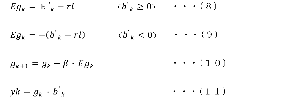
図7は、実施の形態に係る測距装置の信号処理部による信号処理の一例を説明するため図である。信号処理部40は、サンプリング点毎に、周波数の補正量に関する補正用信号S4を生成可能に構成される。信号処理部40は、サンプリング点毎のビート信号に基づいて、複数のサンプリング点にそれぞれ対応する複数の補正用信号S4を生成し、記憶部55に記憶させる。
記憶部55は、複数のサンプリング点の数に応じた数のメモリを有する。記憶部55では、サンプリング点とそのサンプリング点における補正値を示す補正用信号S4とが対応付けられ、そのサンプリング点に対応するメモリに記憶される。
例えば、信号処理部40は、図7に模式的に示すように、一のアップチャープ期間におけるビート信号と次のアップチャープ期間におけるビート信号との比較をチャープ期間毎に繰り返すことで、チャープレートの誤差を求め、チャープレートの補正量を学習する。また、信号処理部40は、一のダウンチャープ期間におけるビート信号と次のダウンチャープ期間におけるビート信号との比較をチャープ期間毎に繰り返し、チャープレートの補正量を学習する。
このように、信号処理部40は、位相比較部43及び演算部48等によって、ビート信号の位相誤差を検出し、補正用信号S4を記憶部55に記憶させる。サンプリング点毎に検出される位相誤差に応じて、記憶部55に記憶される補正用信号S4が更新され、チャープレートの補正量を学習することができる。測距装置1は、メモリ学習型ILC(Iterative Learning control)によるpre-distortion動作を行うことができる。
時刻kにおけるチャープレートの誤差δγ/γkは、次式(12)で表すことができる。なお、Tsは、ビート信号のサンプリング周期である。なお、δTkは、時刻kにおけるサンプリング周期の誤差である。
また、式(12)とテーラー展開の1次近似により、次式(13)が得られる。式(13)に示すように、チャープレートの誤差δγ/γkは、時刻kの位相誤差pe_kと1時刻前である時刻(k―1)の位相誤差pe_(k-1)との差分として表すことができる。

上述した式(12)、(13)に示すように、チャープレートの誤差δγ/γkは、周波数誤差、位相誤差の差分等により表すことができる。例えば、信号処理部40は、補正用信号S4として、ビート信号の周波数誤差を示す信号を生成し、サンプリング点毎に生成した補正用信号S4を記憶部55に記憶させてもよい。また、例えば、信号処理部40は、補正用信号S4として、2つのサンプリング点の各々における位相誤差の差分を示す信号を生成し、サンプリング点毎に生成した補正用信号S4を記憶部55に記憶させるようにしてもよい。
図8は、実施の形態に係る測距装置の信号処理部による位相誤差の差分の検出処理の一例を説明するため図である。なお、図8では、×点は、サンプリング点のビート信号を示している。また、実線の丸は、次式(14)で表される参照信号rplを示し、点線の丸は、次式(15)で表される参照信号rqlを示している。

参照信号rpl及び参照信号rqlを用いて、時刻kにおけるビート信号ykは、次のように分類することができる。
if (rpl-1 ≧ yk > rql-1) //下り
{
cond = 2;
}
else if (rql-1 ≧ yk > rql) //下り
{
if (yk < rpl+1) cond = 0;
else cond = 1;
}
else if (rql ≧ yk ≧ rpl+1) //下り
{
cond = 3;
}
else if (rpl-1 ≦ yk < rql-1) //上り
{
cond = 2;
}
else if (rql-1 ≦ yk < rql) //上り
{
if (yk ≧ rpl+1) cond = 0;
else cond = 1;
}
else //上り
{
cond = 3;
}
if (rpl-1 ≧ yk > rql-1) //下り
{
cond = 2;
}
else if (rql-1 ≧ yk > rql) //下り
{
if (yk < rpl+1) cond = 0;
else cond = 1;
}
else if (rql ≧ yk ≧ rpl+1) //下り
{
cond = 3;
}
else if (rpl-1 ≦ yk < rql-1) //上り
{
cond = 2;
}
else if (rql-1 ≦ yk < rql) //上り
{
if (yk ≧ rpl+1) cond = 0;
else cond = 1;
}
else //上り
{
cond = 3;
}
信号処理部40は、上述のように決定された「cond」の値と、次式(16)~(19)を用いて、時間軸における位相誤差pekを演算し得る。信号処理部40は、位相誤差pekを算出し、位相誤差pekを示す補正用信号S4を記憶部55に記憶させる。

信号処理部40は、pre-distortion動作を行う場合、記憶部55に記憶された補正用信号S4を、図1に示すスイッチSW2及び加算部61を介して、加算部62へ出力させる。加算部62は、設定部75の出力信号の値(+1又は-1)と補正用信号S4の値とを加算し、加算値を示すデジタル信号である信号S11を生成する。補正用信号S4が加算されることで、ビート信号の位相誤差に応じて補正された信号S11が生成され、補正された信号S11を用いて生成される信号S12がDA変換部85へ出力される。
DA変換部85は、位相誤差に応じて調整された信号S12をアナログ信号に変換し、生成した電圧信号V1を光源部10へ出力する。光源部10は、電圧信号V1に応じてレーザ光である光信号の周波数変調を行う。
こうして、測距装置1は、位相誤差が小さくなるようにpre-distortion動作を行うことができる。図9に示す例のように、信号処理部40及び記憶部55等によるILCによってチャープ線形化学習が行われ、チャープレートを適切に補正することが可能となる。
測距装置1では、補正用信号S4に応じて電圧信号V1が変化し、光源部10の光信号の周波数変調量が調整される。光信号の周波数が直線的に連続して変化するように、光信号の周波数変調量を補正することができる。これにより、光信号の周波数変調特性が悪化することを抑制し、測距精度を向上させることが可能となる。
[作用・効果]
本実施の形態に係る測距装置(測距装置1)は、周波数変調された光信号を出力可能な光源部(光源部10)と、光信号と遅延された光信号とに基づくビート信号を検出可能な検出部(検出部20)と、ビート信号をサンプリング点毎にサンプリングし、AD変換を実行可能なAD変換部(AD変換部30)と、デジタル信号に変換されたビート信号に基づいて、光信号の周波数の補正量に関する第1信号(例えば補正用信号S4)を生成可能な信号処理部(信号処理部40)と、複数のサンプリング点にそれぞれ対応する複数の第1信号を記憶可能な記憶部(記憶部55)と、記憶部に記憶された第1信号に基づいて、光信号の周波数変調を制御可能な制御部(制御部90)とを備える。
本実施の形態に係る測距装置(測距装置1)は、周波数変調された光信号を出力可能な光源部(光源部10)と、光信号と遅延された光信号とに基づくビート信号を検出可能な検出部(検出部20)と、ビート信号をサンプリング点毎にサンプリングし、AD変換を実行可能なAD変換部(AD変換部30)と、デジタル信号に変換されたビート信号に基づいて、光信号の周波数の補正量に関する第1信号(例えば補正用信号S4)を生成可能な信号処理部(信号処理部40)と、複数のサンプリング点にそれぞれ対応する複数の第1信号を記憶可能な記憶部(記憶部55)と、記憶部に記憶された第1信号に基づいて、光信号の周波数変調を制御可能な制御部(制御部90)とを備える。
本実施の形態に係る測距装置1は、複数のサンプリング点にそれぞれ対応する複数の補正用信号S4を記憶可能な記憶部55と、補正用信号S4に基づいて、光信号の周波数変調を制御可能な制御部90を有する。このため、本実施の形態では、光信号の周波数変調特性が悪化することを抑制することができる。周波数変調特性を向上可能な測距装置を実現することが可能となる。メモリ学習型ILCによるpre-distortionによってチャープレートを適切に補正することができ、測距性能を向上させることが可能となる。
本実施の形態に係る信号処理部40は、サンプリング点毎のビート信号と参照信号とに基づいて第1信号(例えば補正用信号S3)を生成可能である。このため、本実施の形態では、補正用信号S3を用いてOPLL動作を行うことができ、光信号の周波数変調量を適切に補正することができる。周波数変調特性を改善可能な測距装置を実現することが可能となる。光信号の周波数変調特性が悪化することを防ぎ、測距性能を向上させることが可能となる。
AD変換部30は、ビート信号の周波数の整数倍の周波数でビート信号をサンプリングし、AD変換を行うことが可能である。このため、サンプリング点が減少してPLLによる追従動作が正しく行われなくなることを防ぐことができる。測距装置1は、光信号の周波数変調特性が悪化することを抑制することができる。
干渉部15における遅延時間τMZIが小さく、チャープ帯域幅Δf(チャープ周波数の変調範囲)が小さい場合であっても、OPLL動作を行うことができ、チャープレートを適切に補正することができる。このため、デバイスの小型化(干渉部15、光源部10等の小型化)を実現することが可能となる。例えば、測距装置1は、干渉部15の遅延時間τMZI≦3ns、光源部10による光信号のチャープ帯域幅Δf≦1GHzとなるように構成されてもよい。この場合も、OPLLによる追従動作が正しく行われなくなることを防ぎ、測距性能の低下を抑制することが可能となる。
<2.変形例>
上述した実施の形態では、測距装置1の構成例について説明したが、あくまでも一例であって、測距装置1の構成は、上述した例に限られない。例えば、測距装置1は、上述したOPLL動作及びpre-distortion動作のいずれか一方のみを実行可能に構成されてもよい。また、例えば、測距装置1は、スイッチSW1及びスイッチSW2を共にオン状態とし、OPLL動作及びpre-distortion動作の両方を同時に(並行して)行うようにしてもよい。この場合、測距装置1は、加算部61によって補正用信号S3と補正用信号S4とを加算し、加算された補正用信号に基づいて周波数変調量の補正を行ってもよい。
上述した実施の形態では、測距装置1の構成例について説明したが、あくまでも一例であって、測距装置1の構成は、上述した例に限られない。例えば、測距装置1は、上述したOPLL動作及びpre-distortion動作のいずれか一方のみを実行可能に構成されてもよい。また、例えば、測距装置1は、スイッチSW1及びスイッチSW2を共にオン状態とし、OPLL動作及びpre-distortion動作の両方を同時に(並行して)行うようにしてもよい。この場合、測距装置1は、加算部61によって補正用信号S3と補正用信号S4とを加算し、加算された補正用信号に基づいて周波数変調量の補正を行ってもよい。
<3.適用例>
本開示に係る技術は、様々な回路、装置に適用することができる。上記の測距装置1、信号処理部40等は、測距を行う様々な装置、回路に利用可能である。本開示に係る技術は、例えば、種々の測距装置、入射する光を検出可能な光検出装置、信号処理装置等として、様々な製品へ応用することができる。
本開示に係る技術は、様々な回路、装置に適用することができる。上記の測距装置1、信号処理部40等は、測距を行う様々な装置、回路に利用可能である。本開示に係る技術は、例えば、種々の測距装置、入射する光を検出可能な光検出装置、信号処理装置等として、様々な製品へ応用することができる。
本開示の一実施形態の光検出装置は、光源部(光源部10)から出力される周波数変調された光信号と遅延された光信号とに基づくビート信号を検出可能な検出部(検出部20)と、ビート信号をサンプリング点毎にサンプリングし、AD変換を実行可能なAD変換部(AD変換部30)と、デジタル信号に変換されたビート信号に基づいて、光信号の周波数の補正量に関する第1信号(例えば補正用信号S4)を生成可能な信号処理部(信号処理部40)と、複数のサンプリング点にそれぞれ対応する複数の第1信号を記憶可能な記憶部(記憶部55)と、記憶部に記憶された第1信号に基づいて、光信号の周波数変調を制御可能な制御部(制御部90)とを備える。このため、光信号の周波数変調特性が悪化することを抑制することができる。周波数変調特性を向上可能な光検出装置を実現することが可能となる。
本開示の一実施形態の信号処理装置は、光源部(光源部10)から出力される周波数変調された光信号と遅延された光信号とに基づくビート信号を検出可能な検出部(検出部20)と、ビート信号をサンプリング点毎にサンプリングし、AD変換を実行可能なAD変換部(AD変換部30)と、デジタル信号に変換されたビート信号に基づいて、光信号の周波数の補正量に関する第1信号(例えば補正用信号S4)を生成可能な信号処理部(信号処理部40)と、複数のサンプリング点にそれぞれ対応する複数の第1信号を記憶可能な記憶部(記憶部55)と、記憶部に記憶された第1信号に基づいて、光信号の周波数変調を制御する信号(例えば電圧信号V1)を出力可能な制御部(制御部90)とを備える。このため、光信号の周波数変調特性が悪化することを抑制することができる。周波数変調特性を向上可能な信号処理装置を実現することが可能となる。
以上、実施の形態および変形例を挙げて本開示を説明したが、本技術は上記実施の形態等に限定されるものではなく、種々の変形が可能である。例えば、上述した変形例は、上記実施の形態の変形例として説明したが、各変形例の構成を適宜組み合わせることができる。
なお、本明細書中に記載された効果はあくまで例示であってその記載に限定されるものではなく、他の効果があってもよい。また、本開示は以下のような構成をとることも可能である。
(1)
周波数変調された光信号を出力可能な光源部と、
前記光信号と遅延された前記光信号とに基づくビート信号を検出可能な検出部と、
前記ビート信号をサンプリング点毎にサンプリングし、AD変換を実行可能なAD変換部と、
デジタル信号に変換された前記ビート信号に基づいて、前記光信号の周波数の補正量に関する第1信号を生成可能な信号処理部と、
複数の前記サンプリング点にそれぞれ対応する複数の前記第1信号を記憶可能な記憶部と、
前記記憶部に記憶された前記第1信号に基づいて、前記光信号の周波数変調を制御可能な制御部と
を備える測距装置。
(2)
前記信号処理部は、デジタル信号に変換されたサンプリング点毎の前記ビート信号に基づいて、複数の前記サンプリング点にそれぞれ対応する複数の前記第1信号を生成可能である
前記(1)に記載の測距装置。
(3)
前記信号処理部は、第1の変調期間における前記ビート信号と、第2の変調期間における前記ビート信号との差分に基づいて、前記第1信号を生成可能である
前記(1)または(2)に記載の測距装置。
(4)
前記信号処理部は、前記第1信号として、前記ビート信号の周波数誤差に関する信号を生成可能である
前記(1)から(3)のいずれか1つに記載の測距装置。
(5)
前記信号処理部は、前記第1信号として、前記ビート信号の位相誤差の差分に関する信号を生成可能である
前記(1)から(4)のいずれか1つに記載の測距装置。
(6)
前記記憶部は、前記複数のサンプリング点の数に応じた数のメモリを有し、前記複数のサンプリング点にそれぞれ対応する前記複数の第1信号を記憶可能である
前記(1)から(5)のいずれか1つに記載の測距装置。
(7)
前記AD変換部は、前記ビート信号の周波数の整数倍の周波数で前記ビート信号をサンプリングし、AD変換を行うことが可能である
前記(1)から(6)のいずれか1つに記載の測距装置。
(8)
前記信号処理部は、サンプリング点毎の前記ビート信号と参照信号とに基づいて前記第1信号を生成可能である
前記(1)から(7)のいずれか1つに記載の測距装置。
(9)
前記信号処理部は、前記第1信号として、前記ビート信号と前記参照信号との位相誤差に関する信号を生成可能である
前記(8)に記載の測距装置。
(10)
前記信号処理部は、サンプリング点毎の前記ビート信号に基づいて、前記参照信号を生成可能である
前記(8)または(9)に記載の測距装置。
(11)
前記信号処理部は、前記ビート信号と複数の参照信号とを比較し、比較結果に基づいて選択した前記参照信号と前記ビート信号との差分に関する前記第1信号を生成可能である
前記(8)から(10)のいずれか1つに記載の測距装置。
(12)
前記AD変換部から出力される前記ビート信号をダウンサンプリング可能なサンプリング部を有する
前記(1)から(11)のいずれか1つに記載の測距装置。
(13)
前記信号処理部は、前記サンプリング部によりダウンサンプリングされた前記ビート信号に基づいて前記第1信号を生成可能である
前記(12)に記載の測距装置。
(14)
前記ビート信号のオフセット補正を実行可能なオフセット補正部を有する
前記(1)から(13)のいずれか1つに記載の測距装置。
(15)
前記信号処理部は、前記オフセット補正部により補正された前記ビート信号に基づいて前記第1信号を生成可能である
前記(14)に記載の測距装置。
(16)
前記ビート信号のゲイン補正を実行可能なゲイン補正部を有する
前記(1)から(15)のいずれか1つに記載の測距装置。
(17)
前記信号処理部は、前記ゲイン補正部により補正された前記ビート信号に基づいて前記第1信号を生成可能である
前記(16)に記載の測距装置。
(18)
前記測距装置は、FMCW方式の測距装置である
前記(1)から(17)のいずれか1つに記載の測距装置。
(19)
光源部から出力される周波数変調された光信号と遅延された前記光信号とに基づくビート信号を検出可能な検出部と、
前記ビート信号をサンプリング点毎にサンプリングし、AD変換を実行可能なAD変換部と、
デジタル信号に変換された前記ビート信号に基づいて、前記光信号の周波数の補正量に関する第1信号を生成可能な信号処理部と、
複数の前記サンプリング点にそれぞれ対応する複数の前記第1信号を記憶可能な記憶部と、
前記記憶部に記憶された前記第1信号に基づいて、前記光信号の周波数変調を制御可能な制御部と
を備える光検出装置。
(20)
光源部から出力される周波数変調された光信号と遅延された前記光信号とに基づくビート信号を検出可能な検出部と、
前記ビート信号をサンプリング点毎にサンプリングし、AD変換を実行可能なAD変換部と、
デジタル信号に変換された前記ビート信号に基づいて、前記光信号の周波数の補正量に関する第1信号を生成可能な信号処理部と、
複数の前記サンプリング点にそれぞれ対応する複数の前記第1信号を記憶可能な記憶部と、
前記記憶部に記憶された前記第1信号に基づいて、前記光信号の周波数変調を制御する信号を出力可能な制御部と
を備える信号処理装置。
(1)
周波数変調された光信号を出力可能な光源部と、
前記光信号と遅延された前記光信号とに基づくビート信号を検出可能な検出部と、
前記ビート信号をサンプリング点毎にサンプリングし、AD変換を実行可能なAD変換部と、
デジタル信号に変換された前記ビート信号に基づいて、前記光信号の周波数の補正量に関する第1信号を生成可能な信号処理部と、
複数の前記サンプリング点にそれぞれ対応する複数の前記第1信号を記憶可能な記憶部と、
前記記憶部に記憶された前記第1信号に基づいて、前記光信号の周波数変調を制御可能な制御部と
を備える測距装置。
(2)
前記信号処理部は、デジタル信号に変換されたサンプリング点毎の前記ビート信号に基づいて、複数の前記サンプリング点にそれぞれ対応する複数の前記第1信号を生成可能である
前記(1)に記載の測距装置。
(3)
前記信号処理部は、第1の変調期間における前記ビート信号と、第2の変調期間における前記ビート信号との差分に基づいて、前記第1信号を生成可能である
前記(1)または(2)に記載の測距装置。
(4)
前記信号処理部は、前記第1信号として、前記ビート信号の周波数誤差に関する信号を生成可能である
前記(1)から(3)のいずれか1つに記載の測距装置。
(5)
前記信号処理部は、前記第1信号として、前記ビート信号の位相誤差の差分に関する信号を生成可能である
前記(1)から(4)のいずれか1つに記載の測距装置。
(6)
前記記憶部は、前記複数のサンプリング点の数に応じた数のメモリを有し、前記複数のサンプリング点にそれぞれ対応する前記複数の第1信号を記憶可能である
前記(1)から(5)のいずれか1つに記載の測距装置。
(7)
前記AD変換部は、前記ビート信号の周波数の整数倍の周波数で前記ビート信号をサンプリングし、AD変換を行うことが可能である
前記(1)から(6)のいずれか1つに記載の測距装置。
(8)
前記信号処理部は、サンプリング点毎の前記ビート信号と参照信号とに基づいて前記第1信号を生成可能である
前記(1)から(7)のいずれか1つに記載の測距装置。
(9)
前記信号処理部は、前記第1信号として、前記ビート信号と前記参照信号との位相誤差に関する信号を生成可能である
前記(8)に記載の測距装置。
(10)
前記信号処理部は、サンプリング点毎の前記ビート信号に基づいて、前記参照信号を生成可能である
前記(8)または(9)に記載の測距装置。
(11)
前記信号処理部は、前記ビート信号と複数の参照信号とを比較し、比較結果に基づいて選択した前記参照信号と前記ビート信号との差分に関する前記第1信号を生成可能である
前記(8)から(10)のいずれか1つに記載の測距装置。
(12)
前記AD変換部から出力される前記ビート信号をダウンサンプリング可能なサンプリング部を有する
前記(1)から(11)のいずれか1つに記載の測距装置。
(13)
前記信号処理部は、前記サンプリング部によりダウンサンプリングされた前記ビート信号に基づいて前記第1信号を生成可能である
前記(12)に記載の測距装置。
(14)
前記ビート信号のオフセット補正を実行可能なオフセット補正部を有する
前記(1)から(13)のいずれか1つに記載の測距装置。
(15)
前記信号処理部は、前記オフセット補正部により補正された前記ビート信号に基づいて前記第1信号を生成可能である
前記(14)に記載の測距装置。
(16)
前記ビート信号のゲイン補正を実行可能なゲイン補正部を有する
前記(1)から(15)のいずれか1つに記載の測距装置。
(17)
前記信号処理部は、前記ゲイン補正部により補正された前記ビート信号に基づいて前記第1信号を生成可能である
前記(16)に記載の測距装置。
(18)
前記測距装置は、FMCW方式の測距装置である
前記(1)から(17)のいずれか1つに記載の測距装置。
(19)
光源部から出力される周波数変調された光信号と遅延された前記光信号とに基づくビート信号を検出可能な検出部と、
前記ビート信号をサンプリング点毎にサンプリングし、AD変換を実行可能なAD変換部と、
デジタル信号に変換された前記ビート信号に基づいて、前記光信号の周波数の補正量に関する第1信号を生成可能な信号処理部と、
複数の前記サンプリング点にそれぞれ対応する複数の前記第1信号を記憶可能な記憶部と、
前記記憶部に記憶された前記第1信号に基づいて、前記光信号の周波数変調を制御可能な制御部と
を備える光検出装置。
(20)
光源部から出力される周波数変調された光信号と遅延された前記光信号とに基づくビート信号を検出可能な検出部と、
前記ビート信号をサンプリング点毎にサンプリングし、AD変換を実行可能なAD変換部と、
デジタル信号に変換された前記ビート信号に基づいて、前記光信号の周波数の補正量に関する第1信号を生成可能な信号処理部と、
複数の前記サンプリング点にそれぞれ対応する複数の前記第1信号を記憶可能な記憶部と、
前記記憶部に記憶された前記第1信号に基づいて、前記光信号の周波数変調を制御する信号を出力可能な制御部と
を備える信号処理装置。
本出願は、日本国特許庁において2022年10月25日に出願された日本特許出願番号2022-170337号を基礎として優先権を主張するものであり、この出願の全ての内容を参照によって本出願に援用する。
当業者であれば、設計上の要件や他の要因に応じて、種々の修正、コンビネーション、サブコンビネーション、および変更を想到し得るが、それらは添付の請求の範囲やその均等物の範囲に含まれるものであることが理解される。
Claims (20)
- 周波数変調された光信号を出力可能な光源部と、
前記光信号と遅延された前記光信号とに基づくビート信号を検出可能な検出部と、
前記ビート信号をサンプリング点毎にサンプリングし、AD変換を実行可能なAD変換部と、
デジタル信号に変換された前記ビート信号に基づいて、前記光信号の周波数の補正量に関する第1信号を生成可能な信号処理部と、
複数の前記サンプリング点にそれぞれ対応する複数の前記第1信号を記憶可能な記憶部と、
前記記憶部に記憶された前記第1信号に基づいて、前記光信号の周波数変調を制御可能な制御部と
を備える測距装置。 - 前記信号処理部は、デジタル信号に変換されたサンプリング点毎の前記ビート信号に基づいて、複数の前記サンプリング点にそれぞれ対応する複数の前記第1信号を生成可能である
請求項1に記載の測距装置。 - 前記信号処理部は、第1の変調期間における前記ビート信号と、第2の変調期間における前記ビート信号との差分に基づいて、前記第1信号を生成可能である
請求項1に記載の測距装置。 - 前記信号処理部は、前記第1信号として、前記ビート信号の周波数誤差に関する信号を生成可能である
請求項1に記載の測距装置。 - 前記信号処理部は、前記第1信号として、前記ビート信号の位相誤差の差分に関する信号を生成可能である
請求項1に記載の測距装置。 - 前記記憶部は、前記複数のサンプリング点の数に応じた数のメモリを有し、前記複数のサンプリング点にそれぞれ対応する複数の前記第1信号を記憶可能である
請求項1に記載の測距装置。 - 前記AD変換部は、前記ビート信号の周波数の整数倍の周波数で前記ビート信号をサンプリングし、AD変換を行うことが可能である
請求項1に記載の測距装置。 - 前記信号処理部は、サンプリング点毎の前記ビート信号と参照信号とに基づいて前記第1信号を生成可能である
請求項7に記載の測距装置。 - 前記信号処理部は、前記第1信号として、前記ビート信号と前記参照信号との位相誤差に関する信号を生成可能である
請求項8に記載の測距装置。 - 前記信号処理部は、サンプリング点毎の前記ビート信号に基づいて、前記参照信号を生成可能である
請求項8に記載の測距装置。 - 前記信号処理部は、前記ビート信号と複数の参照信号とを比較し、比較結果に基づいて選択した前記参照信号と前記ビート信号との差分に関する前記第1信号を生成可能である
請求項8に記載の測距装置。 - 前記AD変換部から出力される前記ビート信号をダウンサンプリング可能なサンプリング部を有する
請求項8に記載の測距装置。 - 前記信号処理部は、前記サンプリング部によりダウンサンプリングされた前記ビート信号に基づいて前記第1信号を生成可能である
請求項12に記載の測距装置。 - 前記ビート信号のオフセット補正を実行可能なオフセット補正部を有する
請求項1に記載の測距装置。 - 前記信号処理部は、前記オフセット補正部により補正された前記ビート信号に基づいて前記第1信号を生成可能である
請求項14に記載の測距装置。 - 前記ビート信号のゲイン補正を実行可能なゲイン補正部を有する
請求項1に記載の測距装置。 - 前記信号処理部は、前記ゲイン補正部により補正された前記ビート信号に基づいて前記第1信号を生成可能である
請求項16に記載の測距装置。 - 前記測距装置は、FMCW方式の測距装置である
請求項1に記載の測距装置。 - 光源部から出力される周波数変調された光信号と遅延された前記光信号とに基づくビート信号を検出可能な検出部と、
前記ビート信号をサンプリング点毎にサンプリングし、AD変換を実行可能なAD変換部と、
デジタル信号に変換された前記ビート信号に基づいて、前記光信号の周波数の補正量に関する第1信号を生成可能な信号処理部と、
複数の前記サンプリング点にそれぞれ対応する複数の前記第1信号を記憶可能な記憶部と、
前記記憶部に記憶された前記第1信号に基づいて、前記光信号の周波数変調を制御可能な制御部と
を備える光検出装置。 - 光源部から出力される周波数変調された光信号と遅延された前記光信号とに基づくビート信号を検出可能な検出部と、
前記ビート信号をサンプリング点毎にサンプリングし、AD変換を実行可能なAD変換部と、
デジタル信号に変換された前記ビート信号に基づいて、前記光信号の周波数の補正量に関する第1信号を生成可能な信号処理部と、
複数の前記サンプリング点にそれぞれ対応する複数の前記第1信号を記憶可能な記憶部と、
前記記憶部に記憶された前記第1信号に基づいて、前記光信号の周波数変調を制御する信号を出力可能な制御部と
を備える信号処理装置。
Applications Claiming Priority (2)
| Application Number | Priority Date | Filing Date | Title |
|---|---|---|---|
| JP2022-170337 | 2022-10-25 | ||
| JP2022170337 | 2022-10-25 |
Publications (1)
| Publication Number | Publication Date |
|---|---|
| WO2024090071A1 true WO2024090071A1 (ja) | 2024-05-02 |
Family
ID=90830475
Family Applications (1)
| Application Number | Title | Priority Date | Filing Date |
|---|---|---|---|
| PCT/JP2023/033837 Ceased WO2024090071A1 (ja) | 2022-10-25 | 2023-09-19 | 測距装置、光検出装置、および信号処理装置 |
Country Status (1)
| Country | Link |
|---|---|
| WO (1) | WO2024090071A1 (ja) |
Citations (7)
| Publication number | Priority date | Publication date | Assignee | Title |
|---|---|---|---|---|
| JPH07270841A (ja) * | 1994-03-31 | 1995-10-20 | Ando Electric Co Ltd | 掃引光周波数発生装置 |
| JP2016114501A (ja) * | 2014-12-16 | 2016-06-23 | 三菱電機株式会社 | レーダ用信号波源 |
| JP6066015B1 (ja) * | 2015-10-01 | 2017-01-25 | 三菱電機株式会社 | 線形性向上処理器 |
| JP2017181269A (ja) * | 2016-03-30 | 2017-10-05 | 株式会社豊田中央研究所 | センサ補正装置及びプログラム |
| WO2017199296A1 (ja) * | 2016-05-16 | 2017-11-23 | 三菱電機株式会社 | Fm-cwレーダおよびfm-cw信号の生成方法 |
| US20180329031A1 (en) * | 2017-04-21 | 2018-11-15 | Futurewei Technologies, Inc. | Frequency nonlinearity calibration in frequency-modulated continuous wave radar |
| WO2021059327A1 (ja) * | 2019-09-24 | 2021-04-01 | 日本電信電話株式会社 | 測距装置 |
-
2023
- 2023-09-19 WO PCT/JP2023/033837 patent/WO2024090071A1/ja not_active Ceased
Patent Citations (7)
| Publication number | Priority date | Publication date | Assignee | Title |
|---|---|---|---|---|
| JPH07270841A (ja) * | 1994-03-31 | 1995-10-20 | Ando Electric Co Ltd | 掃引光周波数発生装置 |
| JP2016114501A (ja) * | 2014-12-16 | 2016-06-23 | 三菱電機株式会社 | レーダ用信号波源 |
| JP6066015B1 (ja) * | 2015-10-01 | 2017-01-25 | 三菱電機株式会社 | 線形性向上処理器 |
| JP2017181269A (ja) * | 2016-03-30 | 2017-10-05 | 株式会社豊田中央研究所 | センサ補正装置及びプログラム |
| WO2017199296A1 (ja) * | 2016-05-16 | 2017-11-23 | 三菱電機株式会社 | Fm-cwレーダおよびfm-cw信号の生成方法 |
| US20180329031A1 (en) * | 2017-04-21 | 2018-11-15 | Futurewei Technologies, Inc. | Frequency nonlinearity calibration in frequency-modulated continuous wave radar |
| WO2021059327A1 (ja) * | 2019-09-24 | 2021-04-01 | 日本電信電話株式会社 | 測距装置 |
Similar Documents
| Publication | Publication Date | Title |
|---|---|---|
| US8937572B2 (en) | Signal generator, oscillator, and radar device | |
| US8836551B2 (en) | Analog digital converter (ADC) and correction circuit and correction method therefor | |
| US7737885B2 (en) | Ramp linearization for FMCW radar using digital down-conversion of a sampled VCO signal | |
| KR101286784B1 (ko) | 무선 장치 및 신호 처리 방법 | |
| US8868379B2 (en) | Measurement apparatus | |
| JP7326730B2 (ja) | 距離速度測定装置 | |
| EP1835258B1 (en) | Digital feedback method for optical gyroscopes | |
| US20110090104A1 (en) | Digital converter for processing resolver signal | |
| KR102169591B1 (ko) | 주파수변조연속파 레이더시스템 및 그 운용방법 | |
| JP7010304B2 (ja) | 測距装置及び制御方法 | |
| KR20000077392A (ko) | 직교복조장치, 방법 및 기록매체 | |
| US12425039B2 (en) | Time-interleaved ADC skew correction | |
| US9112756B1 (en) | System and method for coherent wideband channel generation using multiple received narrowband channels | |
| WO2024090071A1 (ja) | 測距装置、光検出装置、および信号処理装置 | |
| US11009597B2 (en) | Phase noise compensation in digital beamforming radar systems | |
| US20220407528A1 (en) | Methods and systems for atomic clocks with high accuracy and low allan deviation | |
| US20240377514A1 (en) | Long range coherent lidar | |
| JP5018643B2 (ja) | 方位探知装置 | |
| JP5036373B2 (ja) | パルス信号発生装置 | |
| KR20060072892A (ko) | 타이밍 복원 방법 및 타이밍 복원 장치 | |
| KR20230173739A (ko) | 광 센서 장치 | |
| CN116990784A (zh) | 双微环谐振腔型半导体激光器的线性度校正系统 | |
| JP5572590B2 (ja) | 位相特性推定装置並びにそれを備えた位相補正装置及び信号発生装置並びに位相特性推定方法 | |
| US20250208291A1 (en) | Techniques to compensate for phase impairments in lidar systems | |
| JP2024151297A (ja) | Pll回路 |
Legal Events
| Date | Code | Title | Description |
|---|---|---|---|
| 121 | Ep: the epo has been informed by wipo that ep was designated in this application |
Ref document number: 23882284 Country of ref document: EP Kind code of ref document: A1 |
|
| NENP | Non-entry into the national phase |
Ref country code: DE |
|
| 122 | Ep: pct application non-entry in european phase |
Ref document number: 23882284 Country of ref document: EP Kind code of ref document: A1 |
|
| NENP | Non-entry into the national phase |
Ref country code: JP |