WO2024084865A1 - 半導体装置 - Google Patents
半導体装置 Download PDFInfo
- Publication number
- WO2024084865A1 WO2024084865A1 PCT/JP2023/033323 JP2023033323W WO2024084865A1 WO 2024084865 A1 WO2024084865 A1 WO 2024084865A1 JP 2023033323 W JP2023033323 W JP 2023033323W WO 2024084865 A1 WO2024084865 A1 WO 2024084865A1
- Authority
- WO
- WIPO (PCT)
- Prior art keywords
- semiconductor element
- circuit
- semiconductor
- semiconductor device
- pixel
- Prior art date
- Legal status (The legal status is an assumption and is not a legal conclusion. Google has not performed a legal analysis and makes no representation as to the accuracy of the status listed.)
- Ceased
Links
Images








Classifications
-
- H—ELECTRICITY
- H10—SEMICONDUCTOR DEVICES; ELECTRIC SOLID-STATE DEVICES NOT OTHERWISE PROVIDED FOR
- H10F—INORGANIC SEMICONDUCTOR DEVICES SENSITIVE TO INFRARED RADIATION, LIGHT, ELECTROMAGNETIC RADIATION OF SHORTER WAVELENGTH OR CORPUSCULAR RADIATION
- H10F39/00—Integrated devices, or assemblies of multiple devices, comprising at least one element covered by group H10F30/00, e.g. radiation detectors comprising photodiode arrays
- H10F39/10—Integrated devices
- H10F39/12—Image sensors
Definitions
- This disclosure relates to a semiconductor device.
- Japanese Patent Application Laid-Open No. 2003-233693 discloses a semiconductor device serving as a surface-type (surface-illuminated) solid-state imaging device.
- a semiconductor chip is bonded onto a semiconductor substrate via bump electrodes.
- a lens material is formed in an area on the semiconductor substrate other than the area where the bump electrodes are formed.
- Photoelectric conversion elements are arranged on the semiconductor substrate in the area where the lens material is formed. Peripheral circuits for processing signals from the photoelectric conversion elements are formed on the semiconductor chip.
- the semiconductor device comprises a first semiconductor element having a pixel region on one surface on which a plurality of pixels are arranged, a second semiconductor element mounted in a region on the one surface different from the pixel region and having a first circuit electrically connected to the pixels, and a third semiconductor element mounted on the opposite side of the second semiconductor element to the first semiconductor element and having a second circuit electrically connected to the pixels.
- the thickness of the semiconductor substrate of the second semiconductor element in the semiconductor device according to the first embodiment is thinner than the thickness of the semiconductor substrate of the third semiconductor element in the same direction.
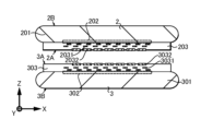
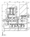
- FIG. 1 is a vertical cross-sectional configuration diagram of a main part of a semiconductor device according to a first embodiment of the present disclosure.
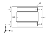
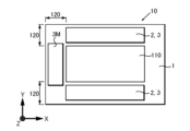
- FIG. 2 is a plan view showing the configuration of the semiconductor device shown in FIG. 3A to 3C are cross-sectional views illustrating a first step of the method for manufacturing a semiconductor device according to the first embodiment.
- FIG. 4 is a cross-sectional view of the second process.
- FIG. 5 is a cross-sectional view of the third process.
- FIG. 6 is a cross-sectional view of the fourth step.
- FIG. 7 is a cross-sectional view of the fifth step.
- FIG. 8 is a cross-sectional view of the sixth step.
- FIG. 1 is a vertical cross-sectional configuration diagram of a main part of a semiconductor device according to a first embodiment of the present disclosure.
- FIG. 2 is a plan view showing the configuration of the semiconductor device shown in FIG. 3A to 3C are cross-sectional views illustrating a first step of the method
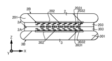
- FIG. 9 is a vertical cross-sectional configuration diagram of a semiconductor device according to a second embodiment of the present disclosure, corresponding to FIG.
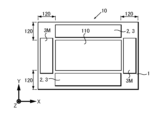
- FIG. 10 is a plan view of the semiconductor device shown in FIG. 9, which corresponds to FIG.
- FIG. 11 is a plan configuration diagram of a semiconductor device according to a third embodiment of the present disclosure
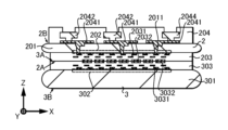
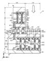
- FIG. 12 is a vertical cross-sectional configuration diagram of a semiconductor device according to a fourth embodiment of the present disclosure
- FIG. 13 is a plan view of the semiconductor device shown in FIG. 12, which corresponds to FIG.
- FIG. 14 is a plan configuration diagram of a semiconductor device according to a fifth embodiment of the present disclosure, corresponding to FIG. FIG.
- FIG. 15 is a plan configuration diagram of a semiconductor device according to the sixth embodiment of the present disclosure, corresponding to FIG.
- FIG. 16 is a vertical cross-sectional configuration diagram of a semiconductor device according to the seventh embodiment of the present disclosure, corresponding to FIG.
- FIG. 17 is a vertical cross-sectional configuration diagram of a semiconductor device according to an eighth embodiment of the present disclosure, corresponding to FIG.
- FIG. 18 is a vertical cross-sectional configuration diagram of a semiconductor device according to a ninth embodiment of the present disclosure, corresponding to FIG.
- FIG. 19 is a system configuration diagram of a semiconductor device according to a tenth embodiment of the present disclosure.
- FIG. 20 is a system configuration diagram of a semiconductor device according to an eleventh embodiment of the present disclosure.
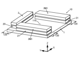
- FIG. 21 is a schematic perspective view of a semiconductor device according to a twelfth embodiment of the present disclosure.
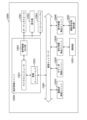
- FIG. 22 is a system configuration diagram of a semiconductor device according to the thirteenth embodiment of the present disclosure.
- 23 is a schematic perspective view of the semiconductor device shown in FIG. 22, which corresponds to FIG.
- FIG. 24 is a block diagram showing an example of a schematic configuration of a vehicle control system.
- FIG. 25 is an explanatory diagram showing an example of the installation positions of the outside-of-vehicle information detection unit and the imaging unit.
- First embodiment a first example in which the present technology is applied to a semiconductor device will be described.
- the semiconductor device is a back-illuminated solid-state imaging device.
- a vertical cross-sectional configuration, a planar configuration, and a manufacturing method of the semiconductor device will be described.
- Second Embodiment a second example in which the mounting structure of the semiconductor element in the semiconductor device according to the first embodiment is changed will be described. 3.
- Third Embodiment in the third embodiment a third example in which the mounting layout of the semiconductor elements in the semiconductor device according to the second embodiment is changed will be described. 4. Fourth Embodiment In the fourth embodiment, a fourth example in which the mounting structure of the semiconductor element in the semiconductor device according to the second embodiment is changed will be described. 5. Fifth Embodiment In the fifth embodiment, a fifth example in which the mounting layout of the semiconductor elements in the semiconductor device according to the first embodiment is changed will be described. 6. Sixth Embodiment In the sixth embodiment, a sixth example in which the mounting layout of the semiconductor elements in the semiconductor device according to the fifth embodiment is changed will be described. 7.
- a seventh example will be described in which a semiconductor element is further added to the semiconductor device according to the first embodiment.
- a semiconductor element is further added to the semiconductor device according to the first embodiment.
- an eighth example in which the semiconductor device according to the first embodiment is applied to a front-illuminated solid-state imaging device will be described.
- a ninth example in which the mounting structure of the semiconductor element in the semiconductor device according to the first embodiment is changed will be described.
- Tenth Embodiment In a tenth embodiment an optimum system configuration will be described in the semiconductor device according to the second embodiment. 11.
- the arrow X direction shown in the drawings indicates one planar direction of the semiconductor device 10 placed on a plane for convenience.
- the arrow Y direction indicates another planar direction perpendicular to the arrow X direction.
- the arrow Z direction indicates an upward direction perpendicular to the arrow X and arrow Y directions.
- the arrow X direction, the arrow Y direction, and the arrow Z direction exactly correspond to the X-axis direction, the Y-axis direction, and the Z-axis direction, respectively, of a three-dimensional coordinate system. Note that these directions are shown to facilitate understanding of the description, and are not intended to limit the directions of the present technology.
- FIG. 1 shows an example of a vertical cross-sectional configuration of a semiconductor device 10 according to the first embodiment.
- Fig. 2 shows an example of a planar configuration of the semiconductor device 10 shown in Fig. 1. 1 and 2, the semiconductor device 10 according to the first embodiment constitutes a back-illuminated solid-state imaging device. More specifically, the semiconductor device 10 is constructed as a CMOS (Complementary Metal Oxide Semiconductor) image sensor.
- the semiconductor device 10 includes a first semiconductor element 1, a second semiconductor element 2, and a third semiconductor element 3 as main components.
- the first semiconductor element 1 includes a pixel region 110 in which a plurality of pixels 100 are arranged on a surface 1A on the side in the direction of the arrow Z.
- the pixels 100 are arranged, for example, in the directions of the arrow X and the arrow Y.
- the surface 1A corresponds to "one surface of the first semiconductor element" according to the present technology.
- the first semiconductor element 1 includes a support substrate 101 and a semiconductor substrate 103 .
- the support substrate 101 is formed of, for example, a single crystal silicon (Si) substrate.
- the side of the support substrate 101 opposite to the direction of the arrow Z is a back surface 1B of the first semiconductor element 1 that faces the front surface 1A.
- the semiconductor substrate 103 is stacked on the Z-direction side of the support substrate 101.
- the semiconductor substrate 103 is formed of, for example, a single crystal Si substrate.
- the thickness of the semiconductor substrate 103 is, for example, 2 ⁇ m or more and 13 ⁇ m or less.
- the semiconductor substrate 103 is laminated on the support substrate 101 with an insulator interposed therebetween. This insulator is formed of, for example, a silicon nitride (SiN) film.
- the support substrate 101 and the semiconductor substrate 103 are each formed in a rectangular shape when viewed from the direction of the arrow Z (hereinafter simply referred to as "in a plan view”) and are formed to have the same planar area (planar size).
- the first semiconductor element 1 is formed as a semiconductor chip processed into a die by dicing a semiconductor wafer during the manufacturing process.
- the planar shape of the first semiconductor element 1 is formed into a rectangular shape with the direction of the arrow X as the longitudinal direction and the direction of the arrow Y as the lateral direction.
- "when viewed in the thickness direction of the first semiconductor element 1" according to the present technology corresponds to "in a plan view viewed in the direction of the arrow Z".
- the pixel region 110 is disposed in the center of the surface 1A of the first semiconductor element 1.
- Each pixel 100 constituting the pixel region 110 includes at least a photoelectric conversion element 107.
- the pixel 100 includes an optical filter 105 and an optical lens 106.
- the photoelectric conversion element 107 is disposed on the semiconductor substrate 103.
- the photoelectric conversion element 107 converts incident light L incident from the direction of the arrow Z into an electric charge.
- the photoelectric conversion element 107 is formed of, for example, a photodiode.
- the optical filter 105 is disposed on the semiconductor substrate 103 on the surface 1A side with an insulator 104 interposed therebetween.
- the optical filter 105 has, for example, color filters of a total of three colors, with each color being different for each pixel 100. That is, the optical filter 105 has a red light filter (R) that transmits light in the red light band, a green light filter (G) that transmits light in the green light band, and a blue light filter (not shown) that transmits light in the blue light band.
- the optical filter 105 is formed, for example, from a resin material containing a dye.
- the optical lens 106 is disposed on the opposite side of the optical filter 105 to the photoelectric conversion element 107. In other words, the optical lens 106 is disposed on the surface 1A side of the optical filter 105. Although not shown in a plan view, the optical lens 106 is formed in a circular shape for each pixel 100. Moreover, when viewed in the direction of the arrow Y for each pixel 100 (hereinafter simply referred to as "in a side view"), the optical lens 106 is formed in a curved shape that curves toward the light incident side and collects the incident light L at the photoelectric conversion element 107.
- the optical lens 106 is formed as a so-called on-chip lens, and is formed for each pixel 100 or integrally across a plurality of pixels 100.
- the optical lens 106 is formed of, for example, a transparent resin material.
- a pixel circuit 108 is electrically connected to one pixel 100 or a plurality of pixels 100 via a transfer transistor (not shown).
- the pixel circuit 108 is configured to include a plurality of transistors Tr.
- the pixel circuit 108 includes transistors Tr used as a reset transistor, an amplification transistor, a select transistor, etc.
- the pixel circuit 108 includes a transfer transistor and is formed of, for example, an n-channel conductive insulated gate field effect transistor (IGFET).
- IGFET n-channel conductive insulated gate field effect transistor
- the wiring layer 102 is disposed on the supporting substrate 101 side of the semiconductor substrate 103. In other words, the wiring layer 102 is disposed just between the semiconductor substrate 103 and the supporting substrate 101.
- multiple layers of wiring 1021 and wiring 1022 are formed to connect between multiple transistors Tr constituting the pixel circuit 108.
- a metal wiring material such as copper (Cu) is used.
- a metal wiring material such as aluminum (Al)-Cu alloy is used.
- a plug wiring 1023 is used to connect the wiring 1021 and the wiring 1022.
- a metal wiring material such as tungsten (W) or Al-Cu alloy is used.
- an insulator 1025 is formed between the multiple layers of wiring 1021, between the wiring 1021 and the wiring 1022, etc.
- the insulator 1025 is formed of, for example, a silicon oxide (SiO 2 ) film.
- a mounting area 120 is disposed in the peripheral portion surrounding the pixel area 110 disposed in the center on the front surface 1A of the first semiconductor element 1.
- a second semiconductor element 2 and a third semiconductor element 3 are mounted in the mounting area 120.
- a plurality of terminals 1042 are disposed in the mounting region 120.
- the terminals 1042 are disposed on a surface portion of the insulator 104 on the arrow Z direction side.
- the terminals 1042 are configured as external terminals that mechanically join and mount the second semiconductor element 2, and also electrically connect the pixels 100 of the first semiconductor element 1 to the first circuit 202 of the second semiconductor element 2.
- the terminals 1042 are also configured as external terminals that electrically connect the pixels 100 and the second circuit 302 of the third semiconductor element 3.
- the terminal 1042 is electrically connected to the wiring 1021 of the wiring layer 102 through a wiring 1041 disposed closer to the semiconductor substrate 103 than the terminal 1042 and a through wiring 1031 penetrating the semiconductor substrate 103 in the thickness direction.
- the terminal 1042, the wiring 1041, and the through wiring 1031 are formed of a metal wiring material such as Cu. Although detailed description is omitted, an insulator 104 is disposed between the terminal 1042 and the wiring 1041. This insulator 104 is used as an interlayer insulating film in the mounting region 120. The insulator 104 is formed of, for example, a SiO2 film.
- the terminal 1042 corresponds to a “first terminal” according to the present technology.
- the pixel 100 is electrically connected to the first circuit 202 of the second semiconductor element 2 through the pixel circuit 108.
- the phrase "the first circuit is electrically connected to the pixel” is used to mean both the pixel 100 being indirectly electrically connected to the first circuit 202 via the pixel circuit 108, and the pixel 100 being directly electrically connected to the first circuit 202.
- a test terminal 1043 is disposed around the pixel region 110 in a region along the periphery of the first semiconductor element 1.
- the terminal 1043 is used for testing electrical characteristics that are performed during or after the manufacturing process of the semiconductor device 10. During testing, a test probe comes into contact with the terminal 1043.
- the terminal 1043 is formed of, for example, the same metal wiring material as the wiring 1022 of the wiring layer 102 .
- the second semiconductor element 2 is mounted in a mounting region 120 on the front surface 1A side of the first semiconductor element 1. In other words, the second semiconductor element 2 is mounted in a region different from the pixel region 110 of the first semiconductor element 1.
- the second semiconductor element 2 includes a semiconductor substrate 201 and a first circuit 202 .
- the semiconductor substrate 201 is formed of, for example, a single crystal Si substrate.
- the thickness of the semiconductor substrate 201 is formed to be thinner than the thickness of the semiconductor substrate 103 of the first semiconductor element 1, and thinner than the semiconductor substrate 301 of the third semiconductor element 3 described below.
- the thickness of the semiconductor substrate 201 is, for example, 10 ⁇ m or less.
- the thickness of the semiconductor substrate 201 is set to, for example, not less than 1 ⁇ m and not more than 10 ⁇ m.
- the first circuit 202 is disposed on the arrow Z direction side (the third semiconductor element 3 side) on the front surface 2A side of the semiconductor substrate 201.
- the first circuit 202 is indirectly electrically connected to the pixels 100 in the pixel region 110 via the pixel circuit 108.
- the first circuit 202 includes one or more logic circuits selected from, for example, a vertical drive circuit, a column signal processing circuit, a horizontal drive circuit, an output circuit, and a control circuit that constitute a peripheral circuit of the back-illuminated solid-state imaging device.
- the first circuit 202 includes a transistor Tr, a resistor, a capacitor, and the like, similar to the pixel circuit 108.
- the second circuit 302 disposed in the third semiconductor element 3 described later includes a divided logic circuit similar to the first circuit 202, or includes another logic circuit not selected in the first circuit 202.
- control circuit receives an input clock and data commanding the operating mode, etc., and outputs data such as internal information of the solid-state imaging device.
- control circuit generates clock signals and control signals that serve as the basis for the operation of the vertical drive circuit, column signal processing circuit, horizontal drive circuit, etc., based on the vertical synchronization signal, horizontal synchronization signal, and master clock. These signals are then input to the vertical drive circuit, column signal processing circuit, horizontal drive circuit, etc.
- the vertical drive circuit is composed of, for example, a shift register.
- the vertical drive circuit selects a pixel drive wiring and supplies a pulse to the selected pixel drive wiring to drive the pixel 100.
- the pixels 100 are driven in row units. That is, the vertical drive circuit sequentially selects and scans each pixel 100 in the pixel region 110 in the vertical direction in row units.
- a signal charge generated in the photoelectric conversion element 107 of each pixel 100 according to the amount of incident light L received through the vertical signal line is supplied to the column signal processing circuit as a pixel signal.
- the column signal processing circuit is arranged, for example, for each column of pixels 100.
- signal processing such as noise removal is performed on the signals output from one row of pixels 100 for each pixel column. That is, the column signal processing circuit performs signal processing such as CDS (Correlated Double Sampling) that removes fixed pattern noise specific to the pixels 100, signal amplification, AD (Analog to Digital) conversion, etc.
- CDS Correlated Double Sampling
- AD Analog to Digital
- the horizontal drive circuit is composed of, for example, a shift register.
- the horizontal drive circuit sequentially outputs horizontal scanning pulses to select each of the column signal processing circuits in turn, and outputs pixel signals from each of the column signal processing circuits to the horizontal signal line.
- the output circuit processes the signals sequentially supplied from each of the column signal processing circuits through the horizontal signal line and outputs the processed signals.
- the output circuit may perform only buffering, black level adjustment, column variation correction, various digital signal processing, etc.
- the logic circuit also includes input/output terminals (not shown).
- the input/output terminals exchange signals between the back-illuminated solid-state imaging device (semiconductor device 10) and the outside.
- the input/output terminals are formed with the same structure as the terminals 1043, and are disposed on the front surface 1A side of the first semiconductor element 1.
- the wiring layer 203 is disposed on the surface 2A side of the semiconductor substrate 201.
- multiple layers of wiring 2031 and terminals 2032 are formed to connect between logic circuits, between the logic circuits and the pixel circuits 108, etc.
- a metal wiring material such as Cu is used for the wiring 2031 and the terminals 2032.
- a plug wiring 2033 is formed which is electrically connected to the transistor Tr of the first circuit 202.
- a metal wiring material such as W is used for the plug wiring 2033.
- insulators 2035 are formed between the multiple layers of wiring 2031, between the wiring 2031 and the terminals 2032, etc.
- the insulators 2035 are formed of, for example, a SiO2 film.
- a surface of the terminal 2032 is exposed from the insulator 2035.
- the terminal 2032 mounts the third semiconductor element 3 and is electrically connected to the terminal 3032.
- the terminal 2032 corresponds to a "third terminal” according to the present technology
- the terminal 3032 corresponds to a "fourth terminal” according to the present technology.
- a wiring layer 204 is disposed on the rear surface 2B side of the semiconductor substrate 201.
- multiple layers of wiring 2041 and terminals 2042 are formed to connect between logic circuits, between logic circuits and pixel circuits 108, etc.
- the wiring 2041 is made of a metal wiring material such as Cu.
- the terminals 2042 are made of a metal wiring material such as an Al-Cu alloy.
- the terminals 2042 are electrically connected to the wiring 2041 via plug wiring 2043.
- the plug wiring 2043 is made of a metal wiring material such as W.
- the terminal 2042 corresponds to a “second terminal” according to the present technology.
- a terminal 2044 for testing is disposed on the wiring layer 204 of the second semiconductor element 2. Like the terminal 1043, the terminal 2044 is used for electrical testing, for example, during the manufacturing process of the semiconductor device 10 or after the manufacturing process is completed.
- the terminal 2044 is formed of, for example, the same metal wiring material as the terminal 2042 of the wiring layer 204 .
- insulators 2045 are formed between the multiple layers of wiring 2041, between the wiring 2041 and the terminals 2042, etc.
- the insulators 2045 are formed of, for example, a SiO2 film.
- the wiring 2401 of the wiring layer 204 is electrically connected to the wiring 2031 of the wiring layer 203 through the through wiring 2011.
- the through wiring 2011 is disposed to penetrate the semiconductor substrate 201 of the second semiconductor element 2 in the thickness direction.
- the through wiring 2011 is formed of, for example, the same metal wiring material as the through wiring 1031.
- the semiconductor substrate 201 is formed thin, so that the through wiring 2011 can be easily provided.
- the through wiring 2011 corresponds to a "first through wiring" according to the present technology.
- the second semiconductor element 2 is mounted on the mounting area 120 on the front surface 2A side of the first semiconductor element 1 using a face-up method in which the first circuit 202 is oriented in the same direction as the arrow Z. More specifically, the second semiconductor element 2 is mounted on the first semiconductor element 1 by electrically connecting the terminal 2042 of the wiring layer 204 of the second semiconductor element 2 to the terminal 1042 disposed in the mounting region 120 of the first semiconductor element 1.
- a bump electrode 5 is used.
- a microbump electrode is used here.
- the bump electrodes 5 are made of Sn-based solder such as a tin (Sn)-silver (Ag) alloy.
- the second semiconductor element 2 has a rectangular planar shape in plan view.
- the planar area (planar size) of the second semiconductor element 2 is smaller than the planar area (planar size) of the first semiconductor element 1.
- the second semiconductor element 2 is disposed within the surface 1A of the first semiconductor element 1. In other words, the second semiconductor element 2 is mounted on the peripheral portion around the pixel region 110 within the surface 1A of the first semiconductor element 1. In the present technology, it is sufficient that the second semiconductor element 2 is mounted along at least one side of the rectangular first semiconductor element 1. In the first embodiment, a total of two second semiconductor elements 2 are mounted along each of two sides of the first semiconductor element 1 that face each other in the direction of the arrow Y.
- the third semiconductor element 3 is mounted on the front surface 2A side of the second semiconductor element 2. That is, the third semiconductor element 3, like the second semiconductor element 2, is mounted in a mounting region 120 different from the pixel region 110 of the first semiconductor element 1.
- the third semiconductor element 3 includes a semiconductor substrate 301 and a second circuit 302 .
- the semiconductor substrate 301 is formed of, for example, a single crystal Si substrate.
- the thickness of the semiconductor substrate 301 is thinner than the thickness of the semiconductor substrate 103 of the first semiconductor element 1, and is thicker than the semiconductor substrate 201 of the second semiconductor element 2 as described above.
- the thickness of the semiconductor substrate 301 is, for example, not less than 100 ⁇ m and not more than 800 ⁇ m.
- the thickness of the semiconductor substrate 301 is set to, for example, not less than 100 ⁇ m and not more than 400 ⁇ m.
- the second circuit 302 is disposed on the opposite side to the direction of the arrow Z (the second semiconductor element 2 side) on the front surface 3A side of the semiconductor substrate 301.
- the second circuit 302 is indirectly electrically connected to the pixels 100 in the pixel region 110 via the pixel circuit 108 or via the pixel circuit 108 and the first circuit 202.
- the second circuit 302 includes a logic circuit.
- the second circuit 302 includes a transistor Tr, a resistor, a capacitor, and the like.
- the wiring layer 303 is disposed on the front surface 3A side of the semiconductor substrate 301.
- multiple layers of wiring 3031 and terminals 3032 that connect logic circuits and the like are formed.
- Metal wiring materials such as Cu are used for the wiring 3031 and the terminals 3032.
- plug wiring 3033 that is electrically connected to the transistor Tr of the second circuit 302 is formed in the wiring 3031.
- Metal wiring materials such as W are used for the plug wiring 3033.
- no wiring layer is provided on the rear surface 2B of the semiconductor substrate 301.
- insulators 3035 are formed between the multiple layers of wiring 3031, between the wiring 3031 and the terminals 3032, etc.
- the insulators 3035 are formed of, for example, a SiO 2 film.
- the surface of the terminal 3032 is exposed from the insulator 3035.
- the terminal 2032 of the second semiconductor element 2 is joined to this terminal 3032.
- the terminal 3032 mounts the third semiconductor element 3 to the second semiconductor element 2 and is electrically connected to the terminal 2032.
- the third semiconductor element 3 is mounted face-down in such a manner that the surface 3A, on which the second circuit 302 is arranged, faces the surface 2A, on which the first circuit 202 of the second semiconductor element 2 is arranged. More specifically, a terminal 3032 electrically connected to the second circuit 302 of the third semiconductor element 3 is joined to a terminal 2032 electrically connected to the first circuit 202 of the second semiconductor element 2.
- a Cu-Cu bond is formed. In other words, the terminal 2032 and the terminal 3032 are mechanically and electrically connected to each other.
- the planar shape of the third semiconductor element 3 is formed in the same rectangular shape as the planar shape of the second semiconductor element 2. Furthermore, the planar area (planar size) of the third semiconductor element 3 is the same as the planar area (planar size) of the second semiconductor element 2.
- the third semiconductor element 3 is mounted in the same mounting position as the mounting position of the second semiconductor element 2. That is, in the first embodiment, the third semiconductor element 3 is mounted on each of the two second semiconductor elements 2.
- a semiconductor substrate 301 of the third semiconductor element 3 and a semiconductor substrate 201 of the second semiconductor element 2 are formed. Both the semiconductor substrate 301 and the semiconductor substrate 201 are in the form of a semiconductor wafer.
- a second circuit 302 is formed on the front surface 3A side of the semiconductor substrate 301, and further a wiring layer 303 is formed on the front surface 3A side of the semiconductor substrate 301.
- a terminal 3032 is formed on the uppermost layer of the wiring layer 303.
- a first circuit 202 is formed on the front surface 2A side of the semiconductor substrate 201, and further a wiring layer 203 is formed thereon.
- a terminal 2032 is formed on the uppermost layer of the wiring layer 203.
- the surface 3A of the semiconductor substrate 301 is placed opposite the surface 2A of the semiconductor substrate 201, and the terminal 2032 is joined to the terminal 3032.
- the second semiconductor element 2 is mounted on the third semiconductor element 3.
- the back surface 2B of the semiconductor substrate 201 of the second semiconductor element 2 is polished, and the semiconductor substrate 201 is thinned.
- a wiring layer 204 is formed on the rear surface 2B side of the semiconductor substrate 201.
- a terminal 2042 and a terminal 2044 are formed on the top layer of the wiring layer 204.
- the terminal 2042 is formed as a terminal for mounting the second semiconductor element 2 on the first semiconductor element 1 (see FIG. 1).
- the terminal 2044 is formed as a terminal for testing.
- a bump electrode 5 is formed on terminal 2042.
- a bump electrode 5 is not formed on terminal 2044.
- the semiconductor substrate 301 and the semiconductor substrate 201 are diced into individual pieces (semiconductor chips).
- the third semiconductor element 3 is formed from the semiconductor substrate 301 including the wiring layer 303
- the second semiconductor element 2 is formed from the semiconductor substrate 201 including the wiring layer 203 and the wiring layer 204.
- the third semiconductor element 3 is mounted on the second semiconductor element 2.
- the second semiconductor element 2 with the third semiconductor element 3 mounted thereon is mounted in the mounting area 120 of the first semiconductor element 1, thereby completing the manufacturing method for the semiconductor device 10 according to the first embodiment and completing the semiconductor device 10.
- the semiconductor device 10 includes a first semiconductor element 1, a second semiconductor element 2, and a third semiconductor element 3, as shown in FIGS.
- the first semiconductor element 1 has a pixel region 110 on a surface 1A in which a plurality of pixels 100 are arranged.
- the second semiconductor element 2 is mounted in a region on the surface 1A different from the pixel region 110, and has a first circuit 202 electrically connected to the pixels 100.
- the region different from the pixel region 110 is a mounting region 120.
- the third semiconductor element 3 is mounted on the second semiconductor element 2 on the opposite side to the first semiconductor element 1, and has a second circuit 302 electrically connected to the pixels 100.
- the second semiconductor element 2 and the third semiconductor element 3 are stacked in a region different from the pixel region 110, and it is possible to improve the packaging density in the thickness direction of the first semiconductor element 1. Therefore, it is possible to improve the packaging density of the peripheral circuits including the first circuit 202 and the second circuit 302 while expanding the pixel region 110.
- the planar area of each of the second semiconductor element 2 and the third semiconductor element 3 is smaller than the planar area of the first semiconductor element 1 when viewed in the thickness direction of the first semiconductor element 1 (in a planar view). This allows the pixel region 110 of the first semiconductor element 1 to be further enlarged.
- the second semiconductor element 2 and the third semiconductor element 3 are each arranged within the surface 1A of the first semiconductor element 1 when viewed in the thickness direction of the first semiconductor element (in a planar view). Therefore, within the front surface 1A of the first semiconductor element 1, the pixel region 110 can be enlarged and the packaging density can be improved.
- the second semiconductor element 2 includes a through wiring (first through wiring) 2011 that penetrates in the thickness direction and electrically connects the pixel 100 and the first circuit 202.
- the through wiring 2011 is formed so as to penetrate the semiconductor substrate 201 of the second semiconductor element 2 in the thickness direction.
- the semiconductor substrate 201 of the second semiconductor element 2 is formed thin, so that the semiconductor substrate 201 can be easily processed.
- the through wiring 2011 penetrating the semiconductor substrate 201 can be easily formed.
- the wiring layer 203 on the front surface 2A side of the semiconductor substrate 201 and the wiring layer 204 on the back surface 2B side are electrically connected through the through wiring 2011. That is, since the second semiconductor element 2 and the third semiconductor element 3 can be mounted on the first semiconductor element 1 in a stacked state, the mounting density of the mounting area 120 can be improved while the pixel area 110 is enlarged.
- the semiconductor device 10 has a terminal (first terminal) 1042 electrically connected to the pixel 100 on the front surface 1A side of the first semiconductor element 1, and has a terminal (second terminal) 2042 electrically connected to the first circuit 202 or the second circuit 302 on the first semiconductor element 1 side of the second semiconductor element 2.
- the terminal 2042 is electrically connected to the terminal 1042 via the bump electrode 5.
- the second semiconductor element 2 is mounted on the first semiconductor element 1 using the bump electrodes 5, so that the area occupied by the mounting region 120 can be reduced compared to the case where mounting is performed using, for example, a bonding wire method. Therefore, the mounting density of the mounting region 120 can be improved while the pixel region 110 is enlarged.
- the semiconductor device 10 has a terminal (third terminal) 2032 electrically connected to the first circuit 202 on the third semiconductor element 3 side of the second semiconductor element 2.
- the semiconductor device 10 has a terminal (fourth terminal) 3032 electrically connected to the second circuit 302 on the second semiconductor element 2 side of the third semiconductor element 3. Then, the terminal 3032 is joined facing the terminal 2032, and the terminal 2032 and the terminal 3032 are electrically connected.
- the third semiconductor element 3 can be mounted within the surface 2A of the second semiconductor element 2, so that the area occupied by the mounting can be reduced. Therefore, the pixel region 110 can be enlarged while the mounting density of the mounting region 120 can be improved.
- the first semiconductor element 1 constitutes a back-illuminated solid-state imaging device.
- the incident light L can be efficiently captured by the photoelectric conversion element 107 in the pixel 100 in the pixel region 110, and therefore the sensitivity characteristics can be improved.
- the first circuit 202 of the second semiconductor element 2 and the second circuit 302 of the third semiconductor element 3 are logic circuits. Therefore, the pixel region 110 can be enlarged while improving the packaging density of the peripheral circuits in the packaging region 120 .
- the first semiconductor element 1 is formed in a rectangular shape when viewed in the thickness direction (in a plan view).
- a pixel region 110 is disposed in the center of the front surface 1A of the first semiconductor element 1, and the second semiconductor element 2 and the third semiconductor element 3 are mounted in a peripheral portion along at least one side of the rectangular shape as a mounting region 120.
- the pixel region 110 can be enlarged, while the packaging density of the peripheral circuits in the packaging region 120 can be improved.
- Second embodiment> A semiconductor device 10 according to a second embodiment of the present disclosure will be described with reference to FIGS.
- components that are the same as or substantially the same as the components of the semiconductor device 10 of the first embodiment are given the same reference numerals, and duplicated explanations are omitted.
- FIG. 9 shows an example of a vertical cross-sectional configuration of a semiconductor device 10 according to the second embodiment.
- Fig. 10 shows an example of a planar configuration of the semiconductor device 10 shown in Fig. 9.
- the semiconductor device 10 according to the second embodiment includes a third semiconductor element 3M having a second circuit 302M in the semiconductor device 10 according to the first embodiment.
- a second semiconductor element 2 is mounted in a mounting area 120 along one side of the first semiconductor element 1 in the direction of the arrow Y, and a third semiconductor element 3 is mounted on this second semiconductor element 2 (see Figures 1 and 2).
- the first circuit 202 of the second semiconductor element 2 and the second circuit 302 of the third semiconductor element 3 form a logic circuit, similar to the first embodiment.
- a second semiconductor element 2 is mounted in a mounting area 120 along another side of the first semiconductor element 1 opposite the direction of the arrow Y, and a third semiconductor element 3M is mounted on this second semiconductor element 2.
- the first circuit 202 of the second semiconductor element 2 constitutes a logic circuit, as in the first embodiment.
- the third semiconductor element 3M has a second circuit 302M, which constitutes a memory circuit.
- the second circuit 302M is a volatile memory circuit or a non-volatile memory circuit that accumulates signals obtained in the pixel region 110.
- the second circuit 302M is a shift register that constitutes a vertical drive circuit, a horizontal drive circuit, etc.
- the third semiconductor element 3M includes a semiconductor substrate 301 and a wiring layer 303.
- the wiring layer 303 has a terminal 3032 disposed thereon.
- the third semiconductor element 3M is mounted on the second semiconductor element 2 by face-down mounting, with terminals 3032 joined to terminals 2032 of the second semiconductor element 2.
- the components other than those described above are the same as or substantially the same as the components of the semiconductor device 10 according to the first embodiment described above.
- the semiconductor device 10 includes a third semiconductor element 3M having a second circuit 302M.
- the second circuit 302M is a memory circuit, so that the system configuration of the back-illuminated solid-state imaging device can be provided with a signal storage function.
- FIG. 11 shows an example of a planar configuration of a semiconductor device 10 according to the third embodiment.
- the semiconductor device 10 according to the third embodiment includes a third semiconductor element 3M having a second circuit 302M, similar to the semiconductor device 10 according to the second embodiment.
- a second semiconductor element 2 is mounted in a mounting area 120 along one side of the first semiconductor element 1 in the direction of the arrow Y, and a third semiconductor element 3M is mounted on the second semiconductor element 2.
- the first circuit 202 of the second semiconductor element 2 constitutes a logic circuit.
- the second circuit 302M of the third semiconductor element 3M constitutes a memory circuit.
- a second semiconductor element 2 is mounted in a mounting area 120 along another side of the first semiconductor element 1 opposite to the direction of the arrow Y, and a third semiconductor element 3M is mounted on this second semiconductor element 2.
- a first circuit 202 of the second semiconductor element 2 constitutes a logic circuit.
- a second circuit 302M of the third semiconductor element 3M constitutes a memory circuit. That is, in the third embodiment, the third semiconductor element 3 is replaced with a third semiconductor element 3M.
- the components other than those described above are the same as or substantially the same as the components of the semiconductor device 10 according to the second embodiment described above.
- FIG. 12 shows an example of a vertical cross-sectional configuration of a semiconductor device 10 according to the fourth embodiment.
- Fig. 13 shows an example of a planar configuration of the semiconductor device 10 shown in Fig. 12.
- the semiconductor device 10 according to the fourth embodiment is configured by combining the semiconductor device 10 according to the first embodiment with the semiconductor device 10 according to the second or third embodiment.
- a second semiconductor element 2 is mounted in a mounting area 120 along one side of the first semiconductor element 1 in the direction of the arrow Y, and a third semiconductor element 3 is mounted on this second semiconductor element 2.
- the first circuit 202 of the second semiconductor element 2 and the second circuit 302 of the third semiconductor element 3 form a logic circuit, similar to the first embodiment.
- a third semiconductor element 3M is directly and independently mounted in a mounting area 120 along another side opposite to the direction of the arrow Y of the first semiconductor element 1.
- the third semiconductor element 3M has a second circuit 302M, and the second circuit 302M constitutes a memory circuit.
- the third semiconductor element 3M has the terminal 3032 mechanically and electrically connected to the terminal 1042 of the mounting region 120 of the first semiconductor element 1 via the bump electrode 5.
- the third semiconductor element 3M is mounted by the face-down method.
- the third semiconductor element 3M corresponds to a “fifth semiconductor element” according to the present technology
- the second circuit 302M corresponds to a “fourth circuit” according to the present technology.
- the components other than those described above are the same or substantially the same as the components of the semiconductor device 10 according to any one of the first to third embodiments described above.
- FIG. 14 shows an example of a planar configuration of a semiconductor device 10 according to the fifth embodiment.
- the semiconductor device 10 according to the fifth embodiment is configured by combining the semiconductor device 10 according to the first embodiment and the semiconductor device 10 according to the fourth embodiment.
- a second semiconductor element 2 is mounted in a mounting area 120 along one side of the first semiconductor element 1 in the direction of the arrow Y, and a third semiconductor element 3 is mounted on this second semiconductor element 2.
- the first circuit 202 of the second semiconductor element 2 and the second circuit 302 of the third semiconductor element 3 form a logic circuit, similar to the first embodiment.
- a second semiconductor element 2 is mounted in a mounting area 120 along another side of the first semiconductor element 1 opposite the direction of the arrow Y, and a third semiconductor element 3 is mounted on this second semiconductor element 2.
- the first circuit 202 of the second semiconductor element 2 and the second circuit 302 of the third semiconductor element 3 form a logic circuit, similar to the first embodiment.
- a third semiconductor element 3M is directly and independently mounted in a mounting area 120 along one side of the first semiconductor element 1 on the side opposite to the direction of the arrow X.
- the third semiconductor element 3M has a second circuit 302M, and the second circuit 302M constitutes a memory circuit.
- the third semiconductor element 3M is mounted on the mounting area 120 of the first semiconductor element 1 with bump electrodes 5 interposed therebetween, similar to the semiconductor device 10 according to the fourth embodiment.
- the components other than those described above are the same as or substantially the same as the components of the semiconductor device 10 according to the first and fourth embodiments described above.
- FIG. 15 shows an example of a planar configuration of a semiconductor device 10 according to the sixth embodiment.
- the semiconductor device 10 according to the sixth embodiment is the semiconductor device 10 according to the fifth embodiment, further comprising a third semiconductor element 3M in a mounting area 120 along another side of the first semiconductor element 1 on the side facing the arrow X direction. That is, in the mounting area 120 of the first semiconductor element 1, the second semiconductor element 2 and the third semiconductor element 3 are mounted on each of the sides facing the arrow Y direction, and the third semiconductor element 3M is mounted on each of the sides facing the arrow X direction.
- the components other than those described above are the same or substantially the same as the components of the semiconductor device 10 according to the first and fifth embodiments described above.
- FIG. 16 shows an example of a vertical cross-sectional configuration of a semiconductor device 10 according to the seventh embodiment.
- the semiconductor device 10 according to the seventh embodiment further includes a fourth semiconductor element 4 in the semiconductor device 10 according to the first embodiment.
- the semiconductor device 10 like the semiconductor device 10 according to the first embodiment, constitutes a back-illuminated solid-state imaging device.
- the fourth semiconductor element 4 is mounted on the back surface 2B side of the first semiconductor element 1.
- the fourth semiconductor element 4 includes a semiconductor substrate 401 and a third circuit 402.
- the semiconductor substrate 401 is formed of, for example, a single crystal Si substrate, similar to the semiconductor substrate 103 of the first semiconductor element 1 .
- the third circuit 402 is disposed on the semiconductor substrate 401 on the front surface 1A side of the first semiconductor element 1.
- the third circuit 402 includes, for example, a divided logic circuit similar to the first circuit 202 or the second circuit 302, or includes another logic circuit not selected in the first circuit 202 or the second circuit 302.
- the third circuit 402 is configured to include a transistor Tr, a resistor, a capacitor, and the like, similar to the pixel circuit 108.
- the third circuit 402 may also be a memory circuit described in the semiconductor device 10 according to the second embodiment.
- a wiring layer 403 is disposed on the surface 1A side of the semiconductor substrate 401.
- multiple layers of wiring 4031 and terminals 4032 that connect logic circuits and the like are formed.
- a metal wiring material such as Cu is used.
- a metal wiring material such as Cu is used.
- a plug wiring 4033 that is electrically connected to the transistor Tr of the third circuit 402 is formed.
- a metal wiring material such as W is used.
- insulators 4035 are formed between the multiple layers of wiring 4031, between the wiring 4031 and the terminal 4032, etc.
- the insulators 4035 are formed of, for example, a SiO 2 film.
- the surface of the terminal 4032 is exposed from the insulator 4035.
- the wiring 1022 of the wiring layer 102 of the first semiconductor element 1 is Cu-Cu bonded to this terminal 4032 as a terminal. That is, similar to the bonding between the terminal 2032 of the second semiconductor element 2 and the terminal 3032 of the third semiconductor element 3, the terminal 4032 is mechanically and electrically connected to the wiring 1022.
- the fourth semiconductor element 4 corresponds to a “fourth semiconductor element” according to the present technology
- the third circuit 402 corresponds to a “third circuit” according to the present technology.
- the components other than those described above are the same as or substantially the same as the components of the semiconductor device 10 according to the first embodiment described above.
- the semiconductor device 10 includes a fourth semiconductor element 4 having a third circuit 402.
- the system configuration of the back-illuminated solid-state imaging device can be expanded by further adding the fourth semiconductor element 4.
- the fourth semiconductor element 4 is mounted on the back surface 1B side of the first semiconductor element 1, it is possible to further improve the mounting density while expanding the pixel region 110 of the semiconductor device 10.
- FIG. 17 shows an example of a vertical cross-sectional configuration of a semiconductor device 10 according to the eighth embodiment. As shown in FIG. 17, the semiconductor device 10 according to the eighth embodiment is an application example of the semiconductor device 10 according to the first embodiment.
- the semiconductor device 10 is configured as a front-illuminated solid-state imaging device. That is, in the first semiconductor element 1, the pixel circuit 108 is disposed on the front surface 1A side of the semiconductor substrate 103.
- the insulator 104 is also used as a wiring layer, and wiring 1041 and terminals 1042 are formed therein.
- a second semiconductor element 2 is mounted in the mounting area 120 of the first semiconductor element 1.
- a third semiconductor element 3 is mounted on the second semiconductor element 2.
- the components other than those described above are the same as or substantially the same as the components of the semiconductor device 10 according to the first embodiment described above.
- the semiconductor device 10 is a first semiconductor element 1 that constitutes a surface-mounted solid-state imaging device, it is possible to increase the mounting density of the peripheral circuits while expanding the pixel area 110.
- FIG. 18 shows an example of a vertical cross-sectional configuration of a semiconductor device 10 according to the ninth embodiment.
- the semiconductor device 10 according to the ninth embodiment includes a through wiring 2012 in the second semiconductor element 2 in the semiconductor device 10 according to the first embodiment.
- the through wiring 2012 corresponds to the "second through wiring" according to the present technology.
- a through-wire 2012 is provided which passes through the semiconductor substrate 201 and the wiring layer 203 in the thickness direction.
- One end of the through-wire 2012 is electrically connected to a wire 2041 disposed in the wiring layer 204 of the second semiconductor element 2.
- the wire 2041 is indirectly electrically connected to the pixel 100 via the pixel circuit 108 of the first semiconductor element 1.
- the other end of the through-wire 2012 is electrically connected to a terminal 3032 of the wiring layer 303 of the third semiconductor element 3.
- the terminal 3032 is electrically connected to the second circuit 302 via a wiring 3031.
- the through wiring 2012 is formed from the same metal wiring material as the through wiring 2011. Furthermore, since the through wiring 2012 effectively electrically connects the wiring 2014 of the second semiconductor element 2 and the wiring 3031 of the third semiconductor element 3, there is no need to bond the terminal 2032 of the second semiconductor element 2 and the terminal 3032 of the third semiconductor element 3.
- the components other than those described above are the same as or substantially the same as the components of the semiconductor device 10 according to the first embodiment described above.
- the semiconductor device 10 includes a through-wiring 1012 that penetrates the second semiconductor element 2. With the semiconductor device 10 configured in this manner, an electrical connection structure between the second semiconductor element 2 and the third semiconductor element 3 can be easily realized.
- Tenth embodiment> A semiconductor device 10 according to a tenth embodiment of the present disclosure will be described with reference to Fig. 19.
- the semiconductor device 10 according to the tenth embodiment to the semiconductor device 10 according to a thirteenth embodiment of the present disclosure, which will be described later, are examples in which an optimal system configuration is constructed.
- FIG. 19 shows an example of a system configuration of a semiconductor device 10 according to the tenth embodiment.
- the semiconductor device 10 of the tenth embodiment includes a pixel region 110, a scanning circuit SSC, a readout circuit REC, and a control circuit COC in the first semiconductor element 1 in the semiconductor device 10 of the second embodiment.
- the scanning circuit SSC includes, for example, one or more selected from a vertical drive circuit and a horizontal drive circuit.
- the readout circuit REC includes a pixel circuit 108 that reads out pixel signals converted from light to electric charges in the pixels 100.
- the first circuit 202 arranged in the second semiconductor element 2 includes an analog-to-digital conversion circuit ADC, an output signal processing circuit OSC, and an output interface circuit OIF.
- the second circuit 302M of the third semiconductor element 3M includes a memory circuit.
- the pixel signals read out by the readout circuit REC are converted from analog signals to digital signals.
- the pixel signals converted into digital signals are temporarily held in a memory circuit.
- the pixel signals are temporarily stored in the memory circuit.
- the output signal processing circuit OSC reads out the pixel signals stored in the memory circuit and converts the pixel signals into a predetermined output signal, which is then output to an external device by the output interface circuit OIF.
- the components other than those described above are the same as or substantially the same as the components of the semiconductor device 10 according to the second embodiment described above.
- the semiconductor device 10 includes a pixel region 110, a scanning circuit SSC, a readout circuit REC, and a control circuit COC in the first semiconductor element 1.
- the semiconductor device 10 includes an analog-to-digital conversion circuit ADC, an output signal processing circuit OSC, and an output interface circuit OIF in the second semiconductor element 2, and a memory circuit in the third semiconductor element 3M. Therefore, the third semiconductor element 3M can be manufactured by a process specific to an independent memory device with respect to the first semiconductor element 1 and the second semiconductor element 2. To explain in detail, the third semiconductor element 3M can be constructed as a semiconductor element using special materials and processes such as high dielectric constant materials and magnetic materials.
- the third semiconductor element 3M can be equipped with memory circuits such as volatile semiconductor memory elements (e.g., DRAM: Dynamic Random Access Memory), magnetoresistive memory (MRAM: Magneto-resistive Random Access Memory), and resistive random access memory (RRAM: Resistive Random access Memory).
- volatile semiconductor memory elements e.g., DRAM: Dynamic Random Access Memory
- MRAM Magnetoresistive memory
- RRAM resistive random access memory
- an optimal system configuration can be constructed by providing a memory circuit in the third semiconductor element 3M.
- a memory circuit in the third semiconductor element 3M.
- no through-wires are formed in the semiconductor substrate 301 in the third semiconductor element 3M (see FIG. 9). That is, in addition to the special materials and processes, the through-wires are an additional new structure. This makes it possible to effectively suppress or prevent deterioration of the characteristics of the memory elements of the memory circuit caused by the formation of the through-wires.
- the first semiconductor element 1 and the second semiconductor element 2 are connected to each other using the through wiring 2011 (see, for example, FIG. 9 ).
- the second semiconductor element 2 and the third semiconductor element 3M are connected to each other using the connection between the terminal 2032 and the terminal 3032 (see, for example, FIG. 9 ).
- circuits other than the memory circuit can be mounted on either the first semiconductor element 1 or the second semiconductor element 2 as appropriate.
- a semiconductor device 10 according to an eleventh embodiment of the present disclosure will be described with reference to Fig. 20.
- the semiconductor device 10 according to the eleventh embodiment is an application example of the semiconductor device 10 according to the tenth embodiment.
- FIG. 20 shows an example of a system configuration of a semiconductor device 10 according to the eleventh embodiment.
- the semiconductor device 10 according to the eleventh embodiment has the analog-to-digital conversion circuit ADC of the semiconductor device 10 according to the tenth embodiment separated into a comparator circuit CP and a counter circuit COU.
- the comparator circuit CP is mounted on the first semiconductor element 1.
- the counter circuit COU is mounted on the second semiconductor element 2 as a first circuit 202.
- the second semiconductor element 2 includes an output interface circuit OIF as the first circuit 202.
- the third semiconductor element 3M includes a memory circuit as a second circuit 302M, and further includes an output signal processing circuit OSC.
- the output signal processing circuit OSC is electrically connected to the memory circuit through wiring 3031 (see FIG. 9; hereinafter, simply referred to as "first wiring 1W").
- the first wiring 1W corresponds to the "first wiring” according to the present technology.
- the output signal processing circuit OSC operates according to a first clock signal CLK1 supplied from the control circuit COC.
- the output interface circuit OIF is electrically connected to the output signal processing circuit OSC through wiring 3031 and wiring 2031 (see FIG. 9; hereinafter simply referred to as "second wiring 2W").
- the second wiring 2W corresponds to the "second wiring” according to the present technology.
- the output interface circuit OIF operates according to a second clock signal CLK2 supplied from the control circuit COC.
- the number of second wirings 2W is smaller than the number of first wirings 1W.
- the clock frequency of the second clock signal CLK2 is higher than the clock frequency of the first clock signal CLK1.
- a large number of signals can be transferred by parallel processing between the memory circuit and the output signal processing circuit OSC. High-speed serial transfer of signals is possible between the output signal processing circuit OSC and the output interface circuit OIF.
- the components other than those described above are the same or substantially the same as the components of the semiconductor device 10 according to the tenth embodiment described above.
- the memory circuit and the output signal processing circuit OSC are disposed in the third semiconductor element 3.
- the operation of the memory circuit and the output signal processing circuit OSC is not synchronized with the cycle of a series of row sequential readout operations in which the vertical scanning circuit selects the pixels 100 (see Fig. 9) row by row, reads out pixel signals from the selected pixels 100, and converts the pixel signals from analog signals to digital signals.
- the memory circuit and the output signal processing circuit OSC operate as a random logic circuit. This causes irregular power supply noise.
- By disposing such a source of power supply noise in the third semiconductor element 3 far away from the pixel 100 it is possible to effectively suppress or prevent the occurrence of power supply noise. Therefore, it is possible to obtain good image quality as a solid-state imaging device.
- the output interface circuit OIF is disposed on the second semiconductor element 2 as shown in Fig. 20.
- the second semiconductor element 2 is mounted adjacent to the first semiconductor element 1 having a terminal 1043 (see Fig. 9) used as an inspection terminal or an external output terminal.
- a terminal 1043 used as an inspection terminal or an external output terminal.
- the output interface circuit OIF operates according to a high-speed second clock signal CLK2.
- CLK2 high-speed second clock signal
- the analog-to-digital conversion circuit ADC is separated into a comparator circuit CP and a counter circuit COU.
- the comparator circuit CP is an analog circuit and is mounted on the first semiconductor element 1.
- the counter circuit COU is a digital circuit and is mounted on the second semiconductor element 2. Since the second semiconductor element 2 thus configured is only a digital circuit block, no analog circuit elements are required, and the circuit block can be easily realized. As a result, the manufacturing cost of the second semiconductor element 2 can be reduced.
- Twelfth embodiment A semiconductor device 10 according to a twelfth embodiment of the present disclosure will be described with reference to Fig. 21.
- the semiconductor device 10 according to the twelfth embodiment is an application example of the semiconductor device 10 according to the tenth embodiment.
- FIG. 21 shows an example of a schematic configuration of a semiconductor device 10 according to the twelfth embodiment.
- the readout circuit REC and the analog-to-digital conversion circuit ADC in the semiconductor device 10 according to the tenth embodiment are distributed and mounted on both the second semiconductor element 2 and the third semiconductor element 3.
- twice as many analog-to-digital conversion circuits ADC can be mounted within a given area of the mounting region 120 of the first semiconductor element 1.
- the components other than those described above are the same or substantially the same as the components of the semiconductor device 10 according to the tenth embodiment described above.
- the readout circuit REC and the analog-to-digital conversion circuit ADC are distributed and mounted on both the second semiconductor element 2 and the third semiconductor element 3. This makes it possible to double the pixel signal readout speed without increasing the chip size of the semiconductor device 10.
- the second semiconductor element 2 and the third semiconductor element 3 can be manufactured with the same structure, which reduces manufacturing costs.
- “manufactured with the same structure” is used to mean that the second semiconductor element 2 and the third semiconductor element 3 are manufactured with the exact same design, development, and manufacturing.
- the twelfth embodiment is an example in which the readout circuit REC and the analog-to-digital conversion circuit ADC are arranged in parallel in each of the second semiconductor element 2 and the third semiconductor element 3.
- the readout circuit REC may be mounted on the first semiconductor element 1
- the analog-to-digital conversion circuit ADC may be arranged in parallel in each of the second semiconductor element 2 and the third semiconductor element 3.
- a semiconductor device 10 according to a thirteenth embodiment of the present disclosure will be described with reference to Figures 22 and 23.
- the semiconductor device 10 according to the thirteenth embodiment is an application example of the semiconductor device 10 according to the eleventh embodiment.
- FIG. 22 shows an example of a system configuration of a semiconductor device 10 according to the thirteenth embodiment.
- the semiconductor device 10 includes a first semiconductor element 1, a second semiconductor element 20 and a second semiconductor element 21, and a third semiconductor element 3 and a third semiconductor element 3M1.
- the first semiconductor element 1 includes a pixel region 110 .
- the second semiconductor element 20 is equipped with a current generating circuit CGC, a negative voltage generating circuit NVG, an intermediate voltage generating circuit IVG, and a vertical scanning circuit VSC as the first circuit 202.
- the current generating circuit CGC and the like equipped on the second semiconductor element 20 are analog circuits.
- the second semiconductor element 21 is equipped with a constant current source circuit CCS, a comparator circuit CP, and a ramp generating circuit LG as the first circuit 202.
- the constant current source circuit CCS and the like equipped on the second semiconductor element 21 are analog circuits, similar to the second semiconductor element 20.
- the third semiconductor element 3 is equipped with a control signal generating circuit CSG, a clock generating circuit CK, a system circuit SC, and a register circuit RG as the second circuit 302.
- the control signal generating circuit CSG and the like equipped on the third semiconductor element 3 are digital circuits.
- the third semiconductor element 3M1 is equipped with a memory circuit as the second circuit 302M, a counter circuit COU, an output signal processing circuit OSC, and an output interface circuit OIF.
- the memory circuit and the like equipped on the third semiconductor element 3M1 are digital circuits.
- control signal generating circuit CSG supplies a divided clock signal to each of the current generating circuit CGC, the negative voltage generating circuit NVG, and the intermediate voltage generating circuit IVG.
- the control signal generating circuit CSG also supplies a row selection signal, a shutter address signal, a read address signal, a latch pulse signal, a reset pulse signal, and the like to the vertical scanning circuit VSC.
- the control signal generating circuit CSG also supplies a control pulse signal to each of the constant current source circuit CCS and the comparator circuit CP, and supplies a SYNC signal to the memory circuit.
- the control signal generating circuit CSG supplies a register reflecting signal to the register circuit RG, and supplies an interrupt signal to the system circuit SC via the advanced peripheral bus (APB) and the interface (IF).
- API advanced peripheral bus
- IF interface
- FIG. 23 shows an example of a schematic configuration of the semiconductor device 10 shown in FIG.
- a second semiconductor element 21 and a third semiconductor element 3M1 are mounted in a stacked manner.
- a second semiconductor element 20 and a third semiconductor element 3 are mounted in a stacked manner.
- the components other than those described above are the same as or substantially the same as the components of the semiconductor device 10 according to the eleventh embodiment described above.
- a pixel region 110 is provided in the first semiconductor element 1.
- An analog circuit is provided in the second semiconductor element 20 and the second semiconductor element 21, and a digital circuit is provided in the third semiconductor element 3 and the third semiconductor element 3M1.
- a system circuit SC and a clock generation circuit CK that perform overall control of the semiconductor device 10 are disposed in the third semiconductor element 3. For this reason, in order to supply control signals and clock signals to digital circuits other than those described above in the third semiconductor element 3 and analog circuits in the second semiconductor element 2, etc., a structure is required in which signals first pass from the third semiconductor element 3 through the second semiconductor element 2 and the first semiconductor element 1.
- the first semiconductor element 1 has a structure dedicated to pixels and is manufactured by a process dedicated to pixels.
- the second semiconductor element 20 and the second semiconductor element 21 have a structure dedicated to analog circuits and are manufactured by a process dedicated to analog circuits.
- the third semiconductor element 3 and the third semiconductor element 3M1 have a structure dedicated to digital circuits and are manufactured by a process dedicated to digital circuits.
- the first semiconductor element 1, the second semiconductor element 20 and the second semiconductor element 21, and the third semiconductor element 3 and the third semiconductor element 3M1 have device structures that are completely independent of one another and are manufactured by semiconductor manufacturing processes.
- a structure specialized for pixel characteristics can be adopted in the first semiconductor element 1, and a process specialized for pixel characteristics can be adopted.
- a structure specialized for high voltage and low noise can be adopted, and a process specialized for high voltage and low noise can be adopted.
- a structure specialized for low voltage miniaturization can be adopted, and a process specialized for low voltage miniaturization can be adopted. That is, each semiconductor element can be individually optimized, and the overall performance of the semiconductor device 10 can be improved.
- the technology according to the present disclosure can be applied to various products.
- the technology according to the present disclosure may be realized as a device mounted on any type of moving body such as an automobile, an electric vehicle, a hybrid electric vehicle, a motorcycle, a bicycle, a personal mobility device, an airplane, a drone, a ship, or a robot.
- FIG. 24 is a block diagram showing a schematic configuration example of a vehicle control system, which is an example of a mobile object control system to which the technology disclosed herein can be applied.
- the vehicle control system 12000 includes a plurality of electronic control units connected via a communication network 12001.
- the vehicle control system 12000 includes a drive system control unit 12010, a body system control unit 12020, an outside vehicle information detection unit 12030, an inside vehicle information detection unit 12040, and an integrated control unit 12050.
- Also shown as functional components of the integrated control unit 12050 are a microcomputer 12051, an audio/video output unit 12052, and an in-vehicle network I/F (Interface) 12053.
- the drive system control unit 12010 controls the operation of devices related to the drive system of the vehicle according to various programs.
- the drive system control unit 12010 functions as a control device for a drive force generating device for generating the drive force of the vehicle, such as an internal combustion engine or a drive motor, a drive force transmission mechanism for transmitting the drive force to the wheels, a steering mechanism for adjusting the steering angle of the vehicle, and a braking device for generating a braking force for the vehicle.
- the body system control unit 12020 controls the operation of various devices installed in the vehicle body according to various programs.
- the body system control unit 12020 functions as a control device for a keyless entry system, a smart key system, a power window device, or various lamps such as headlamps, tail lamps, brake lamps, turn signals, and fog lamps.
- radio waves or signals from various switches transmitted from a portable device that replaces a key can be input to the body system control unit 12020.
- the body system control unit 12020 accepts the input of these radio waves or signals and controls the vehicle's door lock device, power window device, lamps, etc.
- the outside-vehicle information detection unit 12030 detects information outside the vehicle equipped with the vehicle control system 12000.
- the image capturing unit 12031 is connected to the outside-vehicle information detection unit 12030.
- the outside-vehicle information detection unit 12030 causes the image capturing unit 12031 to capture images outside the vehicle and receives the captured images.
- the outside-vehicle information detection unit 12030 may perform object detection processing or distance detection processing for people, cars, obstacles, signs, characters on the road surface, etc. based on the received images.
- the imaging unit 12031 is an optical sensor that receives light and outputs an electrical signal according to the amount of light received.
- the imaging unit 12031 can output the electrical signal as an image, or as distance measurement information.
- the light received by the imaging unit 12031 may be visible light, or may be invisible light such as infrared light.
- the in-vehicle information detection unit 12040 detects information inside the vehicle.
- a driver state detection unit 12041 that detects the state of the driver is connected.
- the driver state detection unit 12041 includes, for example, a camera that captures an image of the driver, and the in-vehicle information detection unit 12040 may calculate the driver's degree of fatigue or concentration based on the detection information input from the driver state detection unit 12041, or may determine whether the driver is dozing off.
- the microcomputer 12051 can calculate control target values for the driving force generating device, steering mechanism, or braking device based on information inside and outside the vehicle acquired by the outside-vehicle information detection unit 12030 or the inside-vehicle information detection unit 12040, and output control commands to the drive system control unit 12010.
- the microcomputer 12051 can perform cooperative control aimed at realizing the functions of an Advanced Driver Assistance System (ADAS), including vehicle collision avoidance or impact mitigation, following driving based on the distance between vehicles, maintaining vehicle speed, vehicle collision warning, or vehicle lane departure warning.
- ADAS Advanced Driver Assistance System
- the microcomputer 12051 can also control the driving force generating device, steering mechanism, braking device, etc. based on information about the surroundings of the vehicle acquired by the outside vehicle information detection unit 12030 or the inside vehicle information detection unit 12040, thereby performing cooperative control aimed at automatic driving, which allows the vehicle to travel autonomously without relying on the driver's operation.
- the microcomputer 12051 can also output control commands to the body system control unit 12030 based on information outside the vehicle acquired by the outside information detection unit 12030. For example, the microcomputer 12051 can control the headlamps according to the position of a preceding vehicle or an oncoming vehicle detected by the outside information detection unit 12030, and perform cooperative control aimed at preventing glare, such as switching high beams to low beams.
- the audio/image output unit 12052 transmits at least one output signal of audio and image to an output device capable of visually or audibly notifying the occupants of the vehicle or the outside of the vehicle of information.
- an audio speaker 12061, a display unit 12062, and an instrument panel 12063 are exemplified as output devices.
- the display unit 12062 may include, for example, at least one of an on-board display and a head-up display.
- FIG. 25 shows an example of the installation position of the imaging unit 12031.
- the imaging unit 12031 includes imaging units 12101, 12102, 12103, 12104, and 12105.
- the imaging units 12101, 12102, 12103, 12104, and 12105 are provided, for example, at the front nose, side mirrors, rear bumper, back door, and upper part of the windshield inside the vehicle cabin of the vehicle 12100.
- the imaging unit 12101 provided at the front nose and the imaging unit 12105 provided at the upper part of the windshield inside the vehicle cabin mainly acquire images of the front of the vehicle 12100.
- the imaging units 12102 and 12103 provided at the side mirrors mainly acquire images of the sides of the vehicle 12100.
- the imaging unit 12104 provided at the rear bumper or back door mainly acquires images of the rear of the vehicle 12100.
- the imaging unit 12105 provided at the upper part of the windshield inside the vehicle cabin is mainly used to detect leading vehicles, pedestrians, obstacles, traffic lights, traffic signs, lanes, etc.
- FIG. 25 shows an example of the imaging ranges of the imaging units 12101 to 12104.
- Imaging range 12111 indicates the imaging range of the imaging unit 12101 provided on the front nose
- imaging ranges 12112 and 12113 indicate the imaging ranges of the imaging units 12102 and 12103 provided on the side mirrors, respectively
- imaging range 12114 indicates the imaging range of the imaging unit 12104 provided on the rear bumper or back door.
- an overhead image of the vehicle 12100 viewed from above is obtained by superimposing the image data captured by the imaging units 12101 to 12104.
- At least one of the imaging units 12101 to 12104 may have a function of acquiring distance information.
- at least one of the imaging units 12101 to 12104 may be a stereo camera consisting of multiple imaging elements, or an imaging element having pixels for detecting phase differences.
- the microcomputer 12051 can obtain the distance to each solid object within the imaging ranges 12111 to 12114 and the change in this distance over time (relative speed with respect to the vehicle 12100) based on the distance information obtained from the imaging units 12101 to 12104, and can extract as a preceding vehicle, in particular, the closest solid object on the path of the vehicle 12100 that is traveling in approximately the same direction as the vehicle 12100 at a predetermined speed (e.g., 0 km/h or faster). Furthermore, the microcomputer 12051 can set the inter-vehicle distance that should be maintained in advance in front of the preceding vehicle, and perform automatic braking control (including follow-up stop control) and automatic acceleration control (including follow-up start control). In this way, cooperative control can be performed for the purpose of automatic driving, which runs autonomously without relying on the driver's operation.
- automatic braking control including follow-up stop control
- automatic acceleration control including follow-up start control
- the microcomputer 12051 classifies and extracts three-dimensional object data on three-dimensional objects, such as two-wheeled vehicles, ordinary vehicles, large vehicles, pedestrians, utility poles, and other three-dimensional objects, based on the distance information obtained from the imaging units 12101 to 12104, and can use the data to automatically avoid obstacles.
- the microcomputer 12051 distinguishes obstacles around the vehicle 12100 into obstacles that are visible to the driver of the vehicle 12100 and obstacles that are difficult to see.
- the microcomputer 12051 determines the collision risk, which indicates the risk of collision with each obstacle, and when the collision risk is equal to or exceeds a set value and there is a possibility of a collision, it can provide driving assistance for collision avoidance by outputting an alarm to the driver via the audio speaker 12061 or the display unit 12062, or by forcibly decelerating or steering to avoid a collision via the drive system control unit 12010.
- At least one of the imaging units 12101 to 12104 may be an infrared camera that detects infrared rays.
- the microcomputer 12051 can recognize a pedestrian by determining whether or not a pedestrian is present in the captured image of the imaging units 12101 to 12104. The recognition of such a pedestrian is performed, for example, by a procedure of extracting feature points in the captured image of the imaging units 12101 to 12104 as infrared cameras, and a procedure of performing pattern matching processing on a series of feature points that indicate the contour of an object to determine whether or not it is a pedestrian.
- the audio/image output unit 12052 controls the display unit 12062 to superimpose a rectangular contour line for emphasis on the recognized pedestrian.
- the audio/image output unit 12052 may also control the display unit 12062 to display an icon or the like indicating a pedestrian at a desired position.
- the above describes an example of a vehicle control system to which the technology disclosed herein can be applied.
- the technology disclosed herein can be applied to the imaging unit 12031 of the configuration described above.
- By applying the technology disclosed herein to the imaging unit 12031 it is possible to realize an imaging unit 12031 that expands the pixel area while improving the packaging density of the peripheral circuitry.
- the present technology is applicable to a semiconductor device including a first semiconductor element having a pixel region in which a plurality of pixels each having a light emitting source that emits light are arranged, where the light emitting source includes, for example, a light emitting diode (LED), a laser, a liquid crystal including a backlight, an organic electroluminescence (EL), plasma, etc.
- the light emitting source includes, for example, a light emitting diode (LED), a laser, a liquid crystal including a backlight, an organic electroluminescence (EL), plasma, etc.
- a semiconductor device includes a first semiconductor element, a second semiconductor element, and a third semiconductor element.
- the first semiconductor element has a pixel region on one surface where a plurality of pixels are arranged
- the second semiconductor element is mounted in a region on the one surface different from the pixel region and has a first circuit electrically connected to the pixels
- the third semiconductor element is mounted on the second semiconductor element on the opposite side to the first semiconductor element and has a second circuit electrically connected to the pixels.
- the second semiconductor element and the third semiconductor element are stacked in a region different from the pixel region, and the packaging density can be improved in the thickness direction of the first semiconductor element, thereby making it possible to increase the packaging density of the peripheral circuits including the first circuit and the second circuit while expanding the pixel region.
- the thickness of the semiconductor substrate of the second semiconductor element is thinner than the thickness of the semiconductor substrate of the third semiconductor element in the same direction.
- the semiconductor substrate of the second semiconductor element can be easily processed, for example, through-hole wiring that penetrates the semiconductor substrate in the thickness direction can be formed. Therefore, the second semiconductor element and the third semiconductor element can be mounted in a stacked state on the first semiconductor element, so that the pixel area can be enlarged while the mounting density of the mounting area can be improved.
- the present technology has the following configuration: According to the present technology having the following configuration, in a semiconductor device, it is possible to increase the packaging density of a packaging region while expanding a pixel region.
- a first semiconductor element having a pixel region on one surface of which a plurality of pixels are arranged; a second semiconductor element mounted in a region of the one surface different from the pixel region and having a first circuit electrically connected to the pixel; a third semiconductor element mounted on the second semiconductor element on an opposite side to the first semiconductor element and having a second circuit electrically connected to the pixel;
- a semiconductor device comprising: (2) The semiconductor device according to (1), wherein the planar area of each of the second semiconductor element and the third semiconductor element is smaller than the planar area of the first semiconductor element when viewed in a thickness direction of the first semiconductor element.
- a fourth semiconductor element is disposed on an opposite side to the one surface of the first semiconductor element, the fourth semiconductor element having a third circuit electrically connected to the pixel and having a planar area equivalent to that of the first semiconductor element when viewed in a thickness direction of the first semiconductor element;
- the first circuit is a logic circuit
- the semiconductor device according to any one of (1) to (11), wherein the second circuit is a memory circuit.
- the semiconductor device according to any one of (1) to (13), wherein a fifth semiconductor element having a fourth circuit electrically connected to the pixel is mounted in a region on the one surface of the first semiconductor element, separate from the pixel region and the mounting region of the second semiconductor element.
- the fourth circuit is a memory circuit.
- the first semiconductor element is formed in a rectangular shape when viewed in a thickness direction
- the semiconductor device according to any one of (1) to (15), wherein the pixel region is arranged in the center of the one surface of the first semiconductor element, and the second semiconductor element and the third semiconductor element are mounted in the peripheral portion along at least one side of a rectangular shape.
- an output interface circuit electrically connected to the output signal processing circuit through a plurality of second wirings, the number of which is smaller than that of the first wirings, and operated by a second clock signal having a higher clock frequency than that of the first clock signal;
- the semiconductor device according to (18), wherein the output interface circuit is disposed in the second semiconductor element as the first circuit.
- an analog circuit is disposed in the first circuit of the second semiconductor element;
- the semiconductor device according to any one of (1) to (19), wherein a digital circuit is disposed in the second circuit of the third semiconductor element.
Landscapes
- Solid State Image Pick-Up Elements (AREA)
Abstract
Description
この半導体装置では、半導体基板上にバンプ電極を介在させて半導体チップが接合されている。半導体基板上のバンプ電極が形成された領域以外の領域には、レンズ材が形成されている。レンズ材が形成された領域において、半導体基板には、光電変換素子が配列されている。半導体チップには、光電変換素子からの信号を処理する周辺回路等が形成されている。
1.第1実施の形態
第1実施の形態は、半導体装置に、本技術を適用した第1例を説明する。第1実施の形態では、半導体装置は、裏面照射型固体撮像装置を構築している。また、第1実施の形態は、半導体装置の縦断面構成、平面構成及び製造方法について説明する。
2.第2実施の形態
第2実施の形態は、第1実施の形態に係る半導体装置において、半導体素子の実装構造を変えた第2例を説明する。
3.第3実施の形態
第3実施の形態は、第2実施の形態に係る半導体装置において、半導体素子の実装レイアウトを変えた第3例を説明する。
4.第4実施の形態
第4実施の形態は、第2実施の形態に係る半導体装置において、半導体素子の実装構造を変えた第4例を説明する。
5.第5実施の形態
第5実施の形態は、第1実施の形態に係る半導体装置において、半導体素子の実装レイアウトを変えた第5例を説明する。
6.第6実施の形態
第6実施の形態は、第5実施の形態に係る半導体装置において、半導体素子の実装レイアウトを変えた第6例を説明する。
7.第7実施の形態
第7実施の形態は、第1実施の形態に係る半導体装置において、更に半導体素子を加えて第7例を説明する。
8.第8実施の形態
第8実施の形態は、第1実施の形態に係る半導体装置を、表面照射型固体撮像装置に適用した第8例を説明する。
9.第9実施の形態
第9実施の形態は、第1実施の形態に係る半導体装置において、半導体素子の実装構造を変えた第9例を説明する。
10.第10実施の形態
第10実施の形態は、第2実施の形態に係る半導体装置において、最適なシステム構成を説明する。
11.第11実施の形態
第11実施の形態は、第10実施の形態に係る半導体装置において、システム構成の第1応用例を説明する。
12.第12実施の形態
第12実施の形態は、第10実施の形態に係る半導体装置において、システム構成の第2応用例を説明する。
13.第13実施の形態
第13実施の形態は、第10実施の形態に係る半導体装置において、システム構成の第3応用例を説明する。
14.移動体への応用例
この応用例は、移動体制御システムの一例である車両制御システムに本技術を適用した例を説明する。
15.その他の実施の形態
図1~図8を用いて、本開示の第1実施の形態に係る半導体装置10を説明する。
なお、これらの各方向は、説明の理解を助けるために示されており、本技術の方向を限定するものではない。
(1)半導体装置10の全体構成
図1は、第1実施の形態に係る半導体装置10の縦断面構成の一例を表している。図2は、図1に示される半導体装置10の平面構成の一例を表している。
図1及び図2に示されるように、第1実施の形態に係る半導体装置10は、裏面照射型固体撮像装置を構築している。さらに詳細に説明すると、半導体装置10は、CMOS(Complementary Metal Oxide Semiconductor)イメージセンサとして構築されている。半導体装置10は、第1半導体素子1と、第2半導体素子2と、第3半導体素子3とを主要な構成要素として備えている。
図1及び図2に示されるように、第1半導体素子1は、矢印Z方向側の表面1Aに画素100が複数配設された画素領域110を備えている。画素100は、例えば矢印X方向及び矢印Y方向に配列されている。ここで、表面1Aとは、本技術に係る「第1半導体素子の一表面」に相当する。
詳しく説明すると、第1半導体素子1は、支持基板101と、半導体基板103とを備えている。
支持基板101は、例えば単結晶珪素(Si)基板により形成されている。支持基板101の矢印Z方向とは反対側は、表面1Aに対向する第1半導体素子1の裏面1Bである。
半導体基板103は、支持基板101の矢印Z方向側に積層されている。半導体基板103は、例えば単結晶Si基板により形成されている。半導体基板103の厚さは、例えば2μm以上13μm以下である。
符号は省略するが、半導体基板103は、支持基板101に絶縁体を介在させて積層されている。この絶縁体は、例えば窒化珪素(SiN)膜により形成されている。
ここで、本技術に係る「第1半導体素子1の厚さ方向から見て」とは、「矢印Z方向から見た平面視において」に相当する。
図1及び図2に示されるように、画素領域110は、第1半導体素子1の表面1Aの中央部に配設されている。画素領域110を構築する個々の画素100は、少なくとも光電変換素子107を備えている。さらに、画素100は、光学フィルタ105と、光学レンズ106とを備えている。
光学レンズ106は、いわゆるオンチップレンズとして形成され、画素100毎に、又は複数の画素100にわたって一体に形成されている。光学レンズ106は、例えば透明樹脂材料により形成されている。
図1に示されるように、1つの画素100又は複数の画素100に対して、図示省略の転送トランジスタを介在させて画素回路108が電気的に接続されている。
画素回路108の詳細な回路構成の図示、側面視においての縦断面構成の図示並びに説明は省略するが、画素回路108は、複数のトランジスタTrを含んで構成されている。例えば、画素回路108は、リセットトランジスタ、増幅トランジスタ、セレクトトランジスタ等に使用されるトランジスタTrを備えている。
転送トランジスタを含み、画素回路108を構成するトランジスタTrは、例えばnチャネル導電型の絶縁ゲート電界効果トランジスタ(IGFET)により形成されている。画素回路108は、半導体基板103の支持基板101側の主面部に配設されている。
半導体基板103の支持基板101側には、配線層102が配設されている。表現を代えると、配線層102は、丁度、半導体基板103と支持基板101との間に配設されている。
配線層102には、例えば画素回路108を構成する複数のトランジスタTr間を結線する複数層の配線1021及び配線1022が形成されている。配線1021には、例えば銅(Cu)等の金属配線材料が使用されている。配線1022には、例えばアルミニウム(Al)-Cu合金等の金属配線材料が使用されている。また、配線1021と配線1022との接続には、プラグ配線1023が使用されている。プラグ配線1023には、例えばタングステン(W)又はAl-Cu合金等の金属配線材料が使用されている。
簡略化されて示されているが、複数層の配線1021間、配線1021と配線1022との間等には、絶縁体1025が形成されている。絶縁体1025は、例えば酸化珪素(SiO2)膜により形成されている。
図1及び図2に示されるように、第1半導体素子1の表面1Aにおいて、中央部に配設された画素領域110の周囲を取り囲む周辺部には、実装領域120が配設されている。実装領域120には、第2半導体素子2及び第3半導体素子3が実装されている。
端子1042は、端子1042よりも半導体基板103側に配設された配線1041及び半導体基板103を厚さ方向に貫通する貫通配線1031を通して、配線層102の配線1021に電気的に接続されている。端子1042、配線1041、貫通配線1031は、例えばCu等の金属配線材料により形成されている。
また、詳細な説明は省略するが、端子1042と配線1041との間には、絶縁体104が配設されている。この絶縁体104は、実装領域120において、層間絶縁膜として使用されている。絶縁体104は、例えばSiO2膜により形成されている。
ここで、端子1042は、本技術に係る「第1端子」に相当する。
端子1043は、例えば配線層102の配線1022と同様の金属配線材料により形成されている。
図1及び図2に示されるように、第2半導体素子2は、第1半導体素子1の表面1A側において、実装領域120に実装されている。つまり、第2半導体素子2は、第1半導体素子1の画素領域110とは異なる領域に実装されている。
第2半導体素子2は、半導体基板201と、第1回路202とを備えている。
半導体基板201は、第1半導体素子1の半導体基板103と同様に、例えば単結晶Si基板により形成されている。ここで、半導体基板201の厚さは、第1半導体素子1の半導体基板103の厚さよりも薄く、かつ、後述する第3半導体素子3の半導体基板301よりも薄く形成されている。半導体基板201の厚さは、例えば10μm以下である。ここでは、半導体基板201の厚さは、例えば1μm以上10μm以下に設定されている。
図1に示されるように、第1回路202は、矢印Z方向側(第3半導体素子3側)であって、半導体基板201の表面2A側に配設されている。第1回路202は、画素領域110の画素100に画素回路108を介在させて間接的に電気的に接続されている。
第1回路202は、裏面照射型固体撮像装置の周辺回路を構築する、例えば垂直駆動回路、カラム信号処理回路、水平駆動回路、出力回路及び制御回路から選択される1又は複数のロジック回路を備えている。第1回路202は、画素回路108と同様に、トランジスタTr、抵抗、容量等を含んで構築されている。なお、後述する第3半導体素子3に配設される第2回路302は、第1回路202と同様のロジック回路が分割されて、又は第1回路202において選択されていない他のロジック回路を備えている。
また、ロジック回路は、図示省略の入出力端子を備えている。入出力端子は、裏面照射型固体撮像装置(半導体装置10)とその外部との信号の遣り取りを行う。ここでは、図示が省略されているが、入出力端子は、端子1043と同一構造により形成され、第1半導体素子1の表面1A側に配設されている。
半導体基板201の表面2A側には、配線層203が配設されている。配線層203には、ロジック回路間、ロジック回路と画素回路108との間等を結線する複数層の配線2031及び端子2032が形成されている。配線2031及び端子2032には、例えばCu等の金属配線材料が使用されている。また、配線2031には、第1回路202のトランジスタTrに電気的に接続されるプラグ配線2033が形成されている。プラグ配線2033には、例えばW等の金属配線材料が使用されている。
ここで、端子2032は、本技術に係る「第3端子」に相当する。また、端子3032は、本技術に係る「第4端子」に相当する。
ここで、端子2042は、本技術に係る「第2端子」に相当する。
端子2044は、例えば配線層204の端子2042と同様の金属配線材料により形成されている。
第2半導体素子2では、半導体基板201が薄く形成されているので、貫通配線2011を簡易に配設することができる。
ここで、貫通配線2011は、本技術に係る「第1貫通配線」に相当する。
図1に示されるように、第1半導体素子1の表面2A側の実装領域120に対して、第2半導体素子2は、第1回路202を同一の矢印Z方向に向けた状態とするフェイスアップ方式により実装されている。
詳しく説明すると、第1半導体素子1の実装領域120に配設された端子1042に、第2半導体素子2の配線層204の端子2042を電気的に接続して、第1半導体素子1に第2半導体素子2が実装されている。この実装には、バンプ電極5が使用されている。バンプ電極5には、ここではマイクロバンプ電極が使用されている。
バンプ電極5には、例えば錫(Sn)-銀(Ag)合金等のSn系半田が使用されている。
第2半導体素子2は、本技術では、矩形状に形成されている第1半導体素子1の少なくとも1つの辺に沿って実装されていればよい。第1実施の形態では、第1半導体素子1の矢印Y方向に対向する2辺のそれぞれに沿って、合計2個の第2半導体素子2が実装されている。
図1及び図2に示されるように、第3半導体素子3は、第2半導体素子2の表面2A側において、実装されている。つまり、第3半導体素子3は、第2半導体素子2と同様に、第1半導体素子1の画素領域110とは異なる実装領域120に実装されている。
第3半導体素子3は、半導体基板301と、第2回路302とを備えている。
半導体基板301は、第1半導体素子1の半導体基板103と同様に、例えば単結晶Si基板により形成されている。ここで、半導体基板301の厚さは、第1半導体素子1の半導体基板103の厚さよりも薄く、かつ、前述の通り第2半導体素子2の半導体基板201よりも厚い。半導体基板301の厚さは、例えば100μm以上800μm以下である。ここでは、半導体基板301の厚さは、例えば100μm以上400μm以下に設定されている。
図1に示されるように、第2回路302は、矢印Z方向とは反対側(第2半導体素子2側)であって、半導体基板301の表面3A側に配設されている。第2回路302は、画素領域110の画素100に画素回路108を介在させて、又は画素回路108及び第1回路202を介在させて間接的に電気的に接続されている。
第2回路302は、前述の通り、ロジック回路を備えている。第2回路302は、画素回路108と同様に、トランジスタTr、抵抗、容量等を含んで構築されている。
半導体基板301の表面3A側には、配線層303が配設されている。配線層303には、ロジック回路間等を結線する複数層の配線3031及び端子3032が形成されている。配線3031及び端子3032には、例えばCu等の金属配線材料が使用されている。また、配線3031には、第2回路302のトランジスタTrに電気的に接続されるプラグ配線3033が形成されている。プラグ配線3033には、例えばW等の金属配線材料が使用されている。
なお、第1実施の形態において、半導体基板301の裏面2Bには、配線層は配設されていない。
図1に示されるように、第2半導体素子2の第1回路202が配設された表面2Aに対して、第3半導体素子3は、第2回路302が配設された表面3Aを向かい合わせた状態とするフェイスダウン方式により実装されている。
詳しく説明すると、第2半導体素子2の第1回路202に電気的に接続された端子2032に、第3半導体素子3の第2回路302に電気的に接続された端子3032が接合されている。ここでは、端子2032、端子3032のいずれにも例えばCuが使用されているので、Cu-Cu接合がなされている。つまり、端子2032、端子3032のそれぞれは、機械的に、かつ、電気的に接続されている。
次に、第1実施の形態に係る半導体装置10の製造方法、特に第1半導体素子1に実装される第2半導体素子2及び第3半導体素子3の製造方法について説明する。図3~図8は、半導体装置10の製造方法を工程毎に説明する工程断面の一例を表している。
半導体基板301の表面3A側には、第2回路302が形成され、更に配線層303が形成される。配線層303の最上層には端子3032が形成される。
一方、半導体基板201の表面2A側には、第1回路202が形成され、更に配線層203が形成される。配線層203の最上層には端子2032が形成される。
以上説明した通り、第1実施の形態に係る半導体装置10は、図1及び図2に示されるように、第1半導体素子1と、第2半導体素子2と、第3半導体素子3とを備える。
第1半導体素子1は、表面1Aに画素100が複数配設された画素領域110を有する。第2半導体素子2は、表面1Aの画素領域110とは異なる領域に実装され、画素100に電気的に接続された第1回路202を有する。ここで、画素領域110とは異なる領域は、実装領域120である。第3半導体素子3は、第2半導体素子2の第1半導体素子1とは反対側に実装され、画素100に電気的に接続された第2回路302を有する。
このように構成される半導体装置10では、画素領域110とは異なる領域において第2半導体素子2及び第3半導体素子3が積層され、第1半導体素子1の厚さ方向に実装密度を向上させることができる。このため、画素領域110を拡大しつつ、第1回路202及び第2回路302を含む周辺回路の実装密度を向上させることができる。
このため、更に第1半導体素子1の画素領域110を拡大することができる。
このため、第1半導体素子1の表面1A内において、画素領域110を拡大しつつ、実装密度を向上させることができる。
このように構成される半導体装置10では、第2半導体素子2の半導体基板201が薄く形成されているので、半導体基板201を簡易に加工可能である。第1実施の形態では、半導体基板201に貫通する貫通配線2011を簡易に形成することができる。このため、第2半導体素子2では、半導体基板201の表面2A側の配線層203と裏面2B側の配線層204とが貫通配線2011を通して電気的に接続される。すなわち、第1半導体素子1に第2半導体素子2、第3半導体素子3のそれぞれを積層状態において実装することができるので、画素領域110を拡大しつつ、実装領域120の実装密度を向上させることができる。
このように構成される半導体装置10では、バンプ電極5を用いて第1半導体素子1に第2半導体素子2が実装されているので、例えばボンディングワイヤ方式を用いて実装する場合よりも、実装領域120の占有面積を縮小することができる。このため、画素領域110を拡大しつつ、実装領域120の実装密度を向上させることができる。
このように構成される半導体装置10では、第2半導体素子2の表面2A内において第3半導体素子3を実装することができるので、実装の占有面積を縮小することができる。このため、画素領域110を拡大しつつ、実装領域120の実装密度を向上させることができる。
このように構成される半導体装置10では、画素領域110の画素100において、光電変換素子107に入射光Lを効率良く取り込めるので、感度特性を向上させることができる。
このため、画素領域110を拡大しつつ、実装領域120において周辺回路の実装密度を向上させることができる。
このように構成される半導体装置10では、画素領域110を拡大しつつ、実装領域120において周辺回路の実装密度を向上させることができる。
図9及び図10を用いて、本開示の第2実施の形態に係る半導体装置10を説明する。
なお、第2実施の形態並びにそれ以降の実施の形態において、第1実施の形態に係る半導体装置10の構成要素と同一の構成要素、又は実質的に同一の構成要素には同一の符号を付し、重複する説明は省略する。
図9は、第2実施の形態に係る半導体装置10の縦断面構成の一例を表している。図10は、図9に示される半導体装置10の平面構成の一例を表している。
第3半導体素子3Mは、第2半導体素子2の端子2032に端子3032を接合し、フェイスダウン方式により第2半導体素子2に実装されている。
第2実施の形態に係る半導体装置10によれば、第1実施の形態に係る半導体装置10により得られる作用効果と同様の作用効果を得ることができる。
図11を用いて、本開示の第3実施の形態に係る半導体装置10を説明する。
図11は、第3実施の形態に係る半導体装置10の平面構成の一例を表している。
図11に示されるように、第3実施の形態に係る半導体装置10は、第2実施の形態に係る半導体装置10と同様に、第2回路302Mを有する第3半導体素子3Mを備えている。詳しく説明すると、第1半導体素子1の矢印Y方向側の1つの辺に沿った実装領域120には、第2半導体素子2が実装され、この第2半導体素子2には第3半導体素子3Mが実装されている。第2半導体素子2の第1回路202は、ロジック回路を構築している。第3半導体素子3Mの第2回路302Mは、メモリ回路を構築している。
すなわち、第3実施の形態では、第3半導体素子3は、第3半導体素子3Mに置き換えられている。
第3実施の形態に係る半導体装置10によれば、第2実施の形態に係る半導体装置10により得られる作用効果と同様の作用効果を得ることができる。
図12及び図13を用いて、本開示の第4実施の形態に係る半導体装置10を説明する。
図12は、第4実施の形態に係る半導体装置10の縦断面構成の一例を表している。図13は、図12に示される半導体装置10の平面構成の一例を表している。
第3半導体素子3Mは、第1半導体素子1の実装領域120の端子1042に、バンプ電極5を介在させて端子3032を機械的に、かつ、電気的に接続している。第3半導体素子3Mは、フェイスダウン方式により実装されている。
ここで、第3半導体素子3Mは、本技術に係る「第5半導体素子」に相当する。また、第2回路302Mは、本技術に係る「第4回路」に相当する。
第4実施の形態に係る半導体装置10によれば、第2実施の形態又は第3実施の形態に係る半導体装置10により得られる作用効果と同様の作用効果を得ることができる。
図14を用いて、本開示の第5実施の形態に係る半導体装置10を説明する。
図14は、第5実施の形態に係る半導体装置10の平面構成の一例を表している。
第3半導体素子3Mは、第4実施の形態に係る半導体装置10と同様に、第1半導体素子1の実装領域120に、バンプ電極5を介在させて実装されている。
第5実施の形態に係る半導体装置10によれば、第4実施の形態に係る半導体装置10により得られる作用効果と同様の作用効果を得ることができる。
図15を用いて、本開示の第6実施の形態に係る半導体装置10を説明する。
図15は、第6実施の形態に係る半導体装置10の平面構成の一例を表している。
第6実施の形態に係る半導体装置10によれば、第5実施の形態に係る半導体装置10により得られる作用効果と同様の作用効果を得ることができる。
図16を用いて、本開示の第6実施の形態に係る半導体装置10を説明する。
図16は、第7実施の形態に係る半導体装置10の縦断面構成の一例を表している。
図16に示されるように、第7実施の形態に係る半導体装置10は、第1実施の形態に係る半導体装置10において、更に第4半導体素子4を備えている。
第3回路402は、第1半導体素子1の表面1A側において、半導体基板401に配設されている。この第3回路402は、例えば第1回路202又は第2回路302と同様のロジック回路が分割されて、又は第1回路202及び第2回路302において選択されていない他のロジック回路を備えている。第3回路402は、画素回路108と同様に、トランジスタTr、抵抗、容量等を含んで構築されている。また、第3回路402は、第2実施の形態に係る半導体装置10において説明したメモリ回路であってもよい。
ここで、第4半導体素子4は、本技術に係る「第4半導体素子」に相当する。また、第3回路402は、本技術に係る「第3回路」に相当する。
第7実施の形態に係る半導体装置10によれば、第1実施の形態に係る半導体装置10により得られる作用効果と同様の作用効果を得ることができる。
図17を用いて、本開示の第8実施の形態に係る半導体装置10を説明する。
図17は、第8実施の形態に係る半導体装置10の縦断面構成の一例を表している。
図17に示されるように、第8実施の形態に係る半導体装置10は、第1実施の形態に係る半導体装置10の応用例である。
第8実施の形態に係る半導体装置10によれば、第1実施の形態に係る半導体装置10により得られる作用効果と同様の作用効果を得ることができる。
図18を用いて、本開示の第9実施の形態に係る半導体装置10を説明する。
図18は、第9実施の形態に係る半導体装置10の縦断面構成の一例を表している。
図18に示されるように、第9実施の形態に係る半導体装置10は、第1実施の形態に係る半導体装置10において、第2半導体素子2に貫通配線2012を備えている。ここで、貫通配線2012は、本技術に係る「第2貫通配線」に相当する。
貫通配線2012の一端は、第2半導体素子2の配線層204に配設された配線2041に電気的に接続されている。配線2041は、第1半導体素子1の画素回路108を介在させて間接的に画素100に電気的に接続されている。
また、貫通配線2012の他端は、第3半導体素子3の配線層303の端子3032に電気的に接続されている。端子3032は、配線3031を介在させて第2回路302に電気的に接続されている。
第9実施の形態に係る半導体装置10によれば、第1実施の形態に係る半導体装置10により得られる作用効果と同様の作用効果を得ることができる。
図19を用いて、本開示の第10実施の形態に係る半導体装置10を説明する。第10実施の形態に係る半導体装置10から後述する本開示の第13実施の形態に係る半導体装置10は、最適なシステム構成を構築した例を説明するものである。
図19は、第10実施の形態に係る半導体装置10のシステム構成の一例を表している。
図19に示されるように、第10実施の形態に係る半導体装置10は、第2実施の形態に係る半導体装置10において、第1半導体素子1に、画素領域110と、走査回路SSCと、読出回路RECと、制御回路COCとを備えている。
走査回路SSCには、例えば垂直駆動回路及び水平駆動回路から選択される1以上が含まれている。また、読出回路RECには、画素100において光から電荷に変換された画素信号を読み出す画素回路108が含まれている。
出力信号処理回路OSCでは、メモリ回路に保持された画素信号を読み出し、この画素信号は所定の出力信号に変換される。出力インターフェース回路OIFでは、この出力信号が外部装置へ出力される。
第10実施の形態に係る半導体装置10によれば、第2実施の形態に係る半導体装置10により得られる作用効果と同様の作用効果を得ることができる。
このため、第3半導体素子3Mは、第1半導体素子1及び第2半導体素子2に対して、独立なメモリデバイスに固有なプロセスにより製作可能となる。詳しく説明すると、高誘電率材料、磁気材料等の特殊な材料やプロセスを利用した半導体素子として、第3半導体素子3Mを構築することができる。具体的には、第3半導体素子3Mには、揮発性の半導体記憶素子(例えば、DRAM:Dynamic Random Access Memory)、磁気抵抗メモリ(MRAM:Magneto-resistive Random Access Memory)、抵抗変化メモリ(RRAM:Resistive Random access Memory)等のメモリ回路が搭載可能となる。
なお、メモリ回路以外の回路は、第1半導体素子1、第2半導体素子2のいずれかに、適宜、搭載可能である。
図20を用いて、本開示の第11実施の形態に係る半導体装置10を説明する。第11実施の形態に係る半導体装置10は、第10実施の形態に係る半導体装置10の応用例である。
図20は、第11実施の形態に係る半導体装置10のシステム構成の一例を表している。
図20に示されるように、第11実施の形態に係る半導体装置10は、第10実施の形態に係る半導体装置10において、アナログデジタル変換回路ADCをコンパレータ回路CPとカウンタ回路COUとに分離している。コンパレータ回路CPは、第1半導体素子1に搭載されている。また、カウンタ回路COUは、第2半導体素子2に第1回路202として搭載されている。さらに、第2半導体素子2は、第1回路202として、出力インターフェース回路OIFを備えている。
そして、第3半導体素子3Mは、第2回路302Mとしてメモリ回路を備え、更に出力信号処理回路OSCを備えている。
第11実施の形態に係る半導体装置10によれば、第10実施の形態に係る半導体装置10により得られる作用効果と同様の作用効果を得ることができる。
このような電源ノイズの発生源が画素100から遠くに離れた第3半導体素子3に配設されることにより、電源ノイズの発生を効果的に抑制又は防止することができる。従って、固体撮像装置として、良好な画質を得ることができる。
このように構成される半導体装置10では、信号伝送の高速化を実現することができる。
このように構成される第2半導体素子2はデジタル回路の回路ブロックのみとなるので、アナログ回路の素子が不要となり、回路ブロックを簡易に実現することができる。結果として、第2半導体素子2の製作費用を削減することができる。
図21を用いて、本開示の第12実施の形態に係る半導体装置10を説明する。第12実施の形態に係る半導体装置10は、第10実施の形態に係る半導体装置10の応用例である。
図21は、第12実施の形態に係る半導体装置10の概略的な構成の一例を表している。
図21に示されるように、第12実施の形態に係る半導体装置10では、第10実施の形態に係る半導体装置10において、読出回路REC及びアナログデジタル変換回路ADCが、第2半導体素子2、第3半導体素子3の双方に分散して搭載されている。表現を代えれば、平面視において、第1半導体素子1の実装領域120の所定面積内に2倍のアナログデジタル変換回路ADCを搭載することができる。
第12実施の形態に係る半導体装置10によれば、第10実施の形態に係る半導体装置10により得られる作用効果と同様の作用効果を得ることができる。
図22及び図23を用いて、本開示の第13実施の形態に係る半導体装置10を説明する。第13実施の形態に係る半導体装置10は、第11実施の形態に係る半導体装置10の応用例である。
図22は、第13実施の形態に係る半導体装置10のシステム構成の一例を表している。
第2半導体素子20には、第1回路202として、電流生成回路CGC、負電圧生成回路NVG、中間電圧生成回路IVG及び垂直走査回路VSCが搭載されている。第2半導体素子20に搭載された電流生成回路CGC等は、アナログ回路である。
また、第2半導体素子21には、第1回路202として、定電流源回路CCS、コンパレータ回路CP及びランプ生成回路LGが搭載されている。第2半導体素子21に搭載された定電流源回路CCS等は、第2半導体素子20と同様に、アナログ回路である。
第3半導体素子3M1には、第2回路302Mとしてのメモリ回路、カウンタ回路COU、出力信号処理回路OSC及び出力インターフェース回路OIFが搭載されている。第3半導体素子3M1に搭載されたメモリ回路等は、デジタル回路である。
さらに、制御信号生成回路CSGは、レジスタ回路RGにレジスタ反映信号を供給し、システム回路SCにアドバンストペリフェラルバス(APB)及びインターフェース(IF)を通して割り込み信号を供給する。
図23は、図22に示される半導体装置10の概略的な構成の一例を表している。
図23に示されるように、第1半導体素子1の矢印X方向に対向するそれぞれの実装領域120には、各々、第2半導体素子21と第3半導体素子3M1とが積層されて実装されている。
さらに、第1半導体素子1の矢印Y方向の実装領域120には、第2半導体素子20と第3半導体素子3とが積層されて実装されている。
第13実施の形態に係る半導体装置10によれば、第11実施の形態に係る半導体装置10により得られる作用効果と同様の作用効果を得ることができる。
第13実施の形態では、半導体装置10の全体の制御を行うシステム回路SCやクロック生成回路CKが第3半導体素子3に配設される。このため、第3半導体素子3の上記以外のデジタル回路、第2半導体素子2のアナログ回路等に制御信号やクロック信号を供給するには、一旦、第3半導体素子3から第2半導体素子2、第1半導体素子1のそれぞれを経由する構造が必要になる。
このため、第1半導体素子1においては、画素特性に特化した構造を採用し、画素特性に特化したプロセスを採用することができる。また、第2半導体素子20、第2半導体素子21のそれぞれにおいては、例えば高耐圧低ノイズに特化した構造を採用し、高耐圧低ノイズに特化したプロセスを採用することができる。さらに、第3半導体素子3、第3半導体素子3M1のそれぞれにおいては、低電圧微細化に特化した構造を採用し、低電圧微細化に特化したプロセスを採用することができる。
つまり、各半導体素子に対して個別に最適化が可能となり、半導体装置10の全体の性能を向上させることができる。
本開示に係る技術(本技術)は、様々な製品へ応用することができる。例えば、本開示に係る技術は、自動車、電気自動車、ハイブリッド電気自動車、自動二輪車、自転車、パーソナルモビリティ、飛行機、ドローン、船舶、ロボット等のいずれかの種類の移動体に搭載される装置として実現されてもよい。
本技術は、上記実施の形態に限定されるものではなく、その要旨を逸脱しない範囲内において、種々変更可能である。
例えば、上記第1実施の形態から第9実施の形態に係る半導体装置のうち、2以上の実施の形態に係る半導体装置を組み合わせてもよい。
さらに、本技術は、光を発する発光源を持つ画素が複数配列された画素領域を有する第1半導体素子を含む半導体装置に適用可能である。ここで、発光源として、例えば発光ダイオード(LED)、レーザ、バックライトを含む液晶、有機エレクトロルミネッセンス(EL)、プラズマ等が含まれている。
第1半導体素子は、一表面に画素が複数配設された画素領域を有する。第2半導体素子は、一表面の画素領域とは異なる領域に実装され、画素に電気的に接続された第1回路を有する。第3半導体素子は、第2半導体素子の第1半導体素子とは反対側に実装され、画素に電気的に接続された第2回路を有する。
このように構成される半導体装置では、画素領域とは異なる領域において第2半導体素子及び第3半導体素子が積層され、第1半導体素子の厚さ方向に実装密度を向上させることができる。このため、画素領域を拡大しつつ、第1回路及び第2回路を含む周辺回路の実装密度を向上させることができる。
このように構成される半導体装置では、第2半導体素子の半導体基板を簡易に加工することができるので、例えば半導体基板を厚さ方向に貫通する貫通配線を形成することができる。このため、第1半導体素子に第2半導体素子、第3半導体素子のそれぞれを積層状態において実装することができるので、画素領域を拡大しつつ、実装領域の実装密度を向上させることができる。
本技術は、以下の構成を備えている。以下の構成の本技術によれば、半導体装置において、画素領域を拡大しつつ、実装領域の実装密度を向上させることができる。
(1)
一表面に画素が複数配設された画素領域を有する第1半導体素子と、
前記一表面の前記画素領域とは異なる領域に実装され、前記画素に電気的に接続された第1回路を有する第2半導体素子と、
前記第2半導体素子の前記第1半導体素子とは反対側に実装され、前記画素に電気的に接続された第2回路を有する第3半導体素子と、
を備えている半導体装置。
(2)
前記第2半導体素子、前記第3半導体素子のそれぞれの平面面積は、前記第1半導体素子の厚さ方向から見て、前記第1半導体素子の平面面積よりも小さい
前記(1)に記載の半導体装置。
(3)
前記第2半導体素子、前記第3半導体素子のそれぞれは、前記第1半導体素子の厚さ方向から見て、前記第1半導体素子の前記一表面内に配設されている
前記(2)に記載の半導体装置。
(4)
前記第2半導体素子の半導体基板の厚さは、前記第3半導体素子の同一方向の半導体基板の厚さよりも薄い
前記(1)から前記(3)のいずれか1つに記載の半導体装置。
(5)
前記第2半導体素子は、厚さ方向に貫通し、前記画素と前記第1回路とを電気的に接続する第1貫通配線を備えている
前記(1)から前記(4)のいずれか1つに記載の半導体装置。
(6)
前記第2半導体素子は、厚さ方向に貫通し、前記画素と前記第2回路とを電気的に接続する第2貫通配線を備えている
前記(1)から前記(5)のいずれか1つに記載の半導体装置。
(7)
前記第1半導体素子の前記一表面側に、前記画素に電気的に接続された第1端子を有し、
前記第2半導体素子の前記第1半導体素子側に、前記第1回路又は前記第2回路に電気的に接続された第2端子を有し、
前記第2端子は、バンプ電極を介在させて、前記第1端子に電気的に接続されている
前記(1)から前記(6)のいずれか1つに記載の半導体装置。
(8)
前記第2半導体素子の前記第3半導体素子側に、前記第1回路に電気的に接続された第3端子を有し、
前記第3半導体素子の前記第2半導体素子側に、前記第2回路に電気的に接続された第4端子を有し、
前記第3端子に向かい合わせて前記第4端子が接合され、前記第3端子と前記第4端子とが電気的に接続されている
前記(1)から前記(5)、前記(7)のいずれか1つに記載の半導体装置。
(9)
前記第1半導体素子は、表面照射型固体撮像装置を構築している
前記(1)から前記(8)のいずれか1つに記載の半導体装置。
(10)
前記第1半導体素子は、裏面照射型固体撮像装置を構築している
前記(1)から前記(8)のいずれか1つに記載の半導体装置。
(11)
前記第1半導体素子の前記一表面とは反対側に、前記画素に電気的に接続された第3回路を有し、前記第1半導体素子の厚さ方向から見て、前記第1半導体素子の平面面積と同等の平面面積を有する第4半導体素子が配設され、
前記第1半導体素子は、裏面照射型固体撮像装置を構築している
前記(1)から前記(8)のいずれか1つに記載の半導体装置。
(12)
前記第1回路及び前記第2回路は、ロジック回路である
前記(1)から前記(11)のいずれか1つに記載の半導体装置。
(13)
前記第1回路は、ロジック回路であり、
前記第2回路は、メモリ回路である
前記(1)から前記(11)のいずれか1つに記載の半導体装置。
(14)
前記第1半導体素子の前記一表面において、前記画素領域及び前記第2半導体素子の実装領域とは別の領域に、前記画素に電気的に接続された第4回路を有する第5半導体素子が実装されている
前記(1)から前記(13)のいずれか1つに記載の半導体装置。
(15)
前記第4回路は、メモリ回路である
前記(14)に記載の半導体装置。
(16)
前記第1半導体素子は、厚さ方向から見て、矩形状に形成され、
前記第1半導体素子の前記一表面の中央部に前記画素領域が配設され、かつ、矩形状の少なくとも1辺に沿った周辺部に前記第2半導体素子及び前記第3半導体素子が実装されている
前記(1)から前記(15)のいずれか1つに記載の半導体装置。
(17)
前記第3半導体素子の前記第2回路は、前記画素から出力された画素信号がアナログデジタル変換された結果を一時的に保持する前記メモリ回路である
前記(13)に記載の半導体装置。
(18)
前記メモリ回路に複数本の第1配線を通して電気的に接続され、第1クロック信号により動作する出力信号処理回路を更に備え、
前記メモリ回路及び前記出力信号処理回路は、前記第3半導体素子に配設されている
前記(13)又は前記(17)に記載の半導体装置。
(19)
前記出力信号処理回路に、前記第1配線よりも配線本数が少ない複数本の第2配線を通して電気的に接続され、前記第1クロック信号よりもクロック周波数が高い第2クロック信号により動作する出力インターフェース回路を更に備え、
前記出力インターフェース回路は、前記第2半導体素子に前記第1回路として配設されている
前記(18)に記載の半導体装置。
(20)
前記第2半導体素子の前記第1回路、前記第3半導体素子の前記第2回路のそれぞれに、アナログデジタル変換回路を備えている
前記(1)から前記(19)のいずれか1つに記載の半導体装置。
(21)
前記第2半導体素子の前記第1回路にアナログ回路が配設され、
前記第3半導体素子の前記第2回路にデジタル回路が配設されている
前記(1)から前記(19)のいずれか1つに記載の半導体装置。
Claims (20)
- 一表面に画素が複数配設された画素領域を有する第1半導体素子と、
前記一表面の前記画素領域とは異なる領域に実装され、前記画素に電気的に接続された第1回路を有する第2半導体素子と、
前記第2半導体素子の前記第1半導体素子とは反対側に実装され、前記画素に電気的に接続された第2回路を有する第3半導体素子と、
を備えている半導体装置。 - 前記第2半導体素子、前記第3半導体素子のそれぞれの平面面積は、前記第1半導体素子の厚さ方向から見て、前記第1半導体素子の平面面積よりも小さい
請求項1に記載の半導体装置。 - 前記第2半導体素子、前記第3半導体素子のそれぞれは、前記第1半導体素子の厚さ方向から見て、前記第1半導体素子の前記一表面内に配設されている
請求項2に記載の半導体装置。 - 前記第2半導体素子の半導体基板の厚さは、前記第3半導体素子の同一方向の半導体基板の厚さよりも薄い
請求項1に記載の半導体装置。 - 前記第2半導体素子は、厚さ方向に貫通し、前記画素と前記第1回路とを電気的に接続する第1貫通配線を備えている
請求項4に記載の半導体装置。 - 前記第2半導体素子は、厚さ方向に貫通し、前記画素と前記第2回路とを電気的に接続する第2貫通配線を備えている
請求項4に記載の半導体装置。 - 前記第1半導体素子の前記一表面側に、前記画素に電気的に接続された第1端子を有し、
前記第2半導体素子の前記第1半導体素子側に、前記第1回路又は前記第2回路に電気的に接続された第2端子を有し、
前記第2端子は、バンプ電極を介在させて、前記第1端子に電気的に接続されている
請求項1に記載の半導体装置。 - 前記第2半導体素子の前記第3半導体素子側に、前記第1回路に電気的に接続された第3端子を有し、
前記第3半導体素子の前記第2半導体素子側に、前記第2回路に電気的に接続された第4端子を有し、
前記第3端子に向かい合わせて前記第4端子が接合され、前記第3端子と前記第4端子とが電気的に接続されている
請求項1に記載の半導体装置。 - 前記第1半導体素子は、表面照射型固体撮像装置を構築している
請求項1に記載の半導体装置。 - 前記第1半導体素子は、裏面照射型固体撮像装置を構築している
請求項1に記載の半導体装置。 - 前記第1半導体素子の前記一表面とは反対側に、前記画素に電気的に接続された第3回路を有し、前記第1半導体素子の厚さ方向から見て、前記第1半導体素子の平面面積と同等の平面面積を有する第4半導体素子が配設され、
前記第1半導体素子は、裏面照射型固体撮像装置を構築している
請求項1に記載の半導体装置。 - 前記第1回路及び前記第2回路は、ロジック回路である
請求項1に記載の半導体装置。 - 前記第1回路は、ロジック回路であり、
前記第2回路は、メモリ回路である
請求項1に記載の半導体装置。 - 前記第1半導体素子の前記一表面において、前記画素領域及び前記第2半導体素子の実装領域とは別の領域に、前記画素に電気的に接続された第4回路を有する第5半導体素子が実装されている
請求項1に記載の半導体装置。 - 前記第4回路は、メモリ回路である
請求項14に記載の半導体装置。 - 前記第1半導体素子は、厚さ方向から見て、矩形状に形成され、
前記第1半導体素子の前記一表面の中央部に前記画素領域が配設され、かつ、矩形状の少なくとも1辺に沿った周辺部に前記第2半導体素子及び前記第3半導体素子が実装されている
請求項1に記載の半導体装置。 - 前記第3半導体素子の前記第2回路は、前記画素から出力された画素信号がアナログデジタル変換された結果を一時的に保持する前記メモリ回路である
請求項13に記載の半導体装置。 - 前記メモリ回路に複数本の第1配線を通して電気的に接続され、第1クロック信号により動作する出力信号処理回路を更に備え、
前記メモリ回路及び前記出力信号処理回路は、前記第3半導体素子に配設されている
請求項13に記載の半導体装置。 - 前記出力信号処理回路に、前記第1配線よりも配線本数が少ない複数本の第2配線を通して電気的に接続され、前記第1クロック信号よりもクロック周波数が高い第2クロック信号により動作する出力インターフェース回路を更に備え、
前記出力インターフェース回路は、前記第2半導体素子に前記第1回路として配設されている
請求項18に記載の半導体装置。 - 前記第2半導体素子の前記第1回路、前記第3半導体素子の前記第2回路のそれぞれに、アナログデジタル変換回路を備えている
請求項1に記載の半導体装置。
Priority Applications (1)
| Application Number | Priority Date | Filing Date | Title |
|---|---|---|---|
| CN202380070804.6A CN120019734A (zh) | 2022-10-19 | 2023-09-13 | 半导体装置 |
Applications Claiming Priority (2)
| Application Number | Priority Date | Filing Date | Title |
|---|---|---|---|
| JP2022-167873 | 2022-10-19 | ||
| JP2022167873 | 2022-10-19 |
Publications (1)
| Publication Number | Publication Date |
|---|---|
| WO2024084865A1 true WO2024084865A1 (ja) | 2024-04-25 |
Family
ID=90737591
Family Applications (1)
| Application Number | Title | Priority Date | Filing Date |
|---|---|---|---|
| PCT/JP2023/033323 Ceased WO2024084865A1 (ja) | 2022-10-19 | 2023-09-13 | 半導体装置 |
Country Status (2)
| Country | Link |
|---|---|
| CN (1) | CN120019734A (ja) |
| WO (1) | WO2024084865A1 (ja) |
Cited By (1)
| Publication number | Priority date | Publication date | Assignee | Title |
|---|---|---|---|---|
| WO2026028778A1 (ja) * | 2024-07-29 | 2026-02-05 | ソニーセミコンダクタソリューションズ株式会社 | 撮像装置、電子機器 |
Citations (8)
| Publication number | Priority date | Publication date | Assignee | Title |
|---|---|---|---|---|
| JP2002289908A (ja) * | 2001-03-26 | 2002-10-04 | Hamamatsu Photonics Kk | 光半導体装置 |
| JP2005012221A (ja) * | 2003-06-18 | 2005-01-13 | Samsung Electronics Co Ltd | 固体撮像用半導体装置 |
| WO2010073520A1 (ja) * | 2008-12-26 | 2010-07-01 | パナソニック株式会社 | 固体撮像デバイスおよびその製造方法 |
| JP2014099582A (ja) * | 2012-10-18 | 2014-05-29 | Sony Corp | 固体撮像装置 |
| JP2015135938A (ja) * | 2013-12-19 | 2015-07-27 | ソニー株式会社 | 半導体装置、半導体装置の製造方法、及び電子機器 |
| JP2016163011A (ja) * | 2015-03-05 | 2016-09-05 | ソニー株式会社 | 半導体装置および製造方法、並びに電子機器 |
| WO2018116864A1 (ja) * | 2016-12-22 | 2018-06-28 | ソニーセミコンダクタソリューションズ株式会社 | 撮像パネル、および撮像パネルの製造方法、レントゲン装置、並びに撮像装置 |
| WO2018198802A1 (ja) * | 2017-04-25 | 2018-11-01 | パナソニックIpマネジメント株式会社 | 固体撮像装置および撮像装置 |
-
2023
- 2023-09-13 CN CN202380070804.6A patent/CN120019734A/zh active Pending
- 2023-09-13 WO PCT/JP2023/033323 patent/WO2024084865A1/ja not_active Ceased
Patent Citations (8)
| Publication number | Priority date | Publication date | Assignee | Title |
|---|---|---|---|---|
| JP2002289908A (ja) * | 2001-03-26 | 2002-10-04 | Hamamatsu Photonics Kk | 光半導体装置 |
| JP2005012221A (ja) * | 2003-06-18 | 2005-01-13 | Samsung Electronics Co Ltd | 固体撮像用半導体装置 |
| WO2010073520A1 (ja) * | 2008-12-26 | 2010-07-01 | パナソニック株式会社 | 固体撮像デバイスおよびその製造方法 |
| JP2014099582A (ja) * | 2012-10-18 | 2014-05-29 | Sony Corp | 固体撮像装置 |
| JP2015135938A (ja) * | 2013-12-19 | 2015-07-27 | ソニー株式会社 | 半導体装置、半導体装置の製造方法、及び電子機器 |
| JP2016163011A (ja) * | 2015-03-05 | 2016-09-05 | ソニー株式会社 | 半導体装置および製造方法、並びに電子機器 |
| WO2018116864A1 (ja) * | 2016-12-22 | 2018-06-28 | ソニーセミコンダクタソリューションズ株式会社 | 撮像パネル、および撮像パネルの製造方法、レントゲン装置、並びに撮像装置 |
| WO2018198802A1 (ja) * | 2017-04-25 | 2018-11-01 | パナソニックIpマネジメント株式会社 | 固体撮像装置および撮像装置 |
Cited By (1)
| Publication number | Priority date | Publication date | Assignee | Title |
|---|---|---|---|---|
| WO2026028778A1 (ja) * | 2024-07-29 | 2026-02-05 | ソニーセミコンダクタソリューションズ株式会社 | 撮像装置、電子機器 |
Also Published As
| Publication number | Publication date |
|---|---|
| CN120019734A (zh) | 2025-05-16 |
Similar Documents
| Publication | Publication Date | Title |
|---|---|---|
| JP7854129B2 (ja) | 固体撮像装置、および、撮像システム | |
| US12349487B2 (en) | Solid-state image pickup device and electronic apparatus | |
| KR20230069909A (ko) | 고체 촬상 장치 및 전자 기기 | |
| CN112602195B (zh) | 摄像装置和电子设备 | |
| US20250201639A1 (en) | Semiconductor device, manufacturing method thereof, and electronic apparatus | |
| CN111886855B (zh) | 摄像装置和电子设备 | |
| WO2024084865A1 (ja) | 半導体装置 | |
| CN114008783B (zh) | 摄像装置 | |
| US20260059881A1 (en) | Photodetection element and electronic apparatus | |
| WO2024101014A1 (ja) | 固体撮像装置 | |
| WO2020071103A1 (ja) | 半導体装置およびその製造方法、撮像素子 | |
| WO2025154626A1 (en) | Semiconductor device | |
| JP2025047905A (ja) | 光検出装置、電子機器及び光検出装置の製造方法 | |
| US20240304648A1 (en) | Solid-state imaging device and manufacturing method for solid-state imaging device | |
| CN121986572A (en) | Light detection device, electronic apparatus, and method of manufacturing light detection device | |
| WO2024135493A1 (ja) | 光検出装置 | |
| WO2026009709A1 (ja) | 光検出装置 | |
| WO2023210329A1 (ja) | 半導体装置及び電子機器 | |
| WO2025126754A1 (ja) | 光検出装置および電子機器 | |
| WO2023090053A1 (ja) | 光検出装置及び電子機器 | |
| WO2024236904A1 (ja) | 光検出装置 | |
| WO2024241891A1 (ja) | 固体撮像装置および電子機器 | |
| CN119522645A (zh) | 半导体装置和电子设备 | |
| WO2023127110A1 (ja) | 光検出装置及び電子機器 |
Legal Events
| Date | Code | Title | Description |
|---|---|---|---|
| 121 | Ep: the epo has been informed by wipo that ep was designated in this application |
Ref document number: 23879515 Country of ref document: EP Kind code of ref document: A1 |
|
| WWE | Wipo information: entry into national phase |
Ref document number: 202380070804.6 Country of ref document: CN |
|
| WWP | Wipo information: published in national office |
Ref document number: 202380070804.6 Country of ref document: CN |
|
| NENP | Non-entry into the national phase |
Ref country code: DE |
|
| 122 | Ep: pct application non-entry in european phase |
Ref document number: 23879515 Country of ref document: EP Kind code of ref document: A1 |
|
| NENP | Non-entry into the national phase |
Ref country code: JP |