WO2024080002A1 - 半導体装置および半導体装置の製造方法 - Google Patents
半導体装置および半導体装置の製造方法 Download PDFInfo
- Publication number
- WO2024080002A1 WO2024080002A1 PCT/JP2023/030566 JP2023030566W WO2024080002A1 WO 2024080002 A1 WO2024080002 A1 WO 2024080002A1 JP 2023030566 W JP2023030566 W JP 2023030566W WO 2024080002 A1 WO2024080002 A1 WO 2024080002A1
- Authority
- WO
- WIPO (PCT)
- Prior art keywords
- region
- protective film
- semiconductor substrate
- semiconductor device
- diode
- Prior art date
- Legal status (The legal status is an assumption and is not a legal conclusion. Google has not performed a legal analysis and makes no representation as to the accuracy of the status listed.)
- Ceased
Links
Images
Classifications
-
- H—ELECTRICITY
- H10—SEMICONDUCTOR DEVICES; ELECTRIC SOLID-STATE DEVICES NOT OTHERWISE PROVIDED FOR
- H10P—GENERIC PROCESSES OR APPARATUS FOR THE MANUFACTURE OR TREATMENT OF DEVICES COVERED BY CLASS H10
- H10P32/00—Diffusion of dopants within, into or out of wafers, substrates or parts of devices
- H10P32/10—Diffusion of dopants within, into or out of semiconductor bodies or layers
- H10P32/18—Diffusion lifetime killers
-
- H—ELECTRICITY
- H10—SEMICONDUCTOR DEVICES; ELECTRIC SOLID-STATE DEVICES NOT OTHERWISE PROVIDED FOR
- H10D—INORGANIC ELECTRIC SEMICONDUCTOR DEVICES
- H10D12/00—Bipolar devices controlled by the field effect, e.g. insulated-gate bipolar transistors [IGBT]
- H10D12/01—Manufacture or treatment
- H10D12/031—Manufacture or treatment of IGBTs
- H10D12/032—Manufacture or treatment of IGBTs of vertical IGBTs
- H10D12/038—Manufacture or treatment of IGBTs of vertical IGBTs having a recessed gate, e.g. trench-gate IGBTs
-
- H—ELECTRICITY
- H10—SEMICONDUCTOR DEVICES; ELECTRIC SOLID-STATE DEVICES NOT OTHERWISE PROVIDED FOR
- H10D—INORGANIC ELECTRIC SEMICONDUCTOR DEVICES
- H10D12/00—Bipolar devices controlled by the field effect, e.g. insulated-gate bipolar transistors [IGBT]
- H10D12/411—Insulated-gate bipolar transistors [IGBT]
- H10D12/441—Vertical IGBTs
- H10D12/461—Vertical IGBTs having non-planar surfaces, e.g. having trenches, recesses or pillars in the surfaces of the emitter, base or collector regions
- H10D12/481—Vertical IGBTs having non-planar surfaces, e.g. having trenches, recesses or pillars in the surfaces of the emitter, base or collector regions having gate structures on slanted surfaces, on vertical surfaces, or in grooves, e.g. trench gate IGBTs
-
- H—ELECTRICITY
- H10—SEMICONDUCTOR DEVICES; ELECTRIC SOLID-STATE DEVICES NOT OTHERWISE PROVIDED FOR
- H10D—INORGANIC ELECTRIC SEMICONDUCTOR DEVICES
- H10D62/00—Semiconductor bodies, or regions thereof, of devices having potential barriers
- H10D62/10—Shapes, relative sizes or dispositions of the regions of the semiconductor bodies; Shapes of the semiconductor bodies
- H10D62/124—Shapes, relative sizes or dispositions of the regions of semiconductor bodies or of junctions between the regions
- H10D62/126—Top-view geometrical layouts of the regions or the junctions
- H10D62/127—Top-view geometrical layouts of the regions or the junctions of cellular field-effect devices, e.g. multicellular DMOS transistors or IGBTs
-
- H—ELECTRICITY
- H10—SEMICONDUCTOR DEVICES; ELECTRIC SOLID-STATE DEVICES NOT OTHERWISE PROVIDED FOR
- H10D—INORGANIC ELECTRIC SEMICONDUCTOR DEVICES
- H10D62/00—Semiconductor bodies, or regions thereof, of devices having potential barriers
- H10D62/50—Physical imperfections
- H10D62/53—Physical imperfections the imperfections being within the semiconductor body
-
- H—ELECTRICITY
- H10—SEMICONDUCTOR DEVICES; ELECTRIC SOLID-STATE DEVICES NOT OTHERWISE PROVIDED FOR
- H10D—INORGANIC ELECTRIC SEMICONDUCTOR DEVICES
- H10D64/00—Electrodes of devices having potential barriers
- H10D64/20—Electrodes characterised by their shapes, relative sizes or dispositions
- H10D64/27—Electrodes not carrying the current to be rectified, amplified, oscillated or switched, e.g. gates
- H10D64/311—Gate electrodes for field-effect devices
- H10D64/411—Gate electrodes for field-effect devices for FETs
- H10D64/511—Gate electrodes for field-effect devices for FETs for IGFETs
- H10D64/517—Gate electrodes for field-effect devices for FETs for IGFETs characterised by the conducting layers
- H10D64/519—Gate electrodes for field-effect devices for FETs for IGFETs characterised by the conducting layers characterised by their top-view geometrical layouts
-
- H—ELECTRICITY
- H10—SEMICONDUCTOR DEVICES; ELECTRIC SOLID-STATE DEVICES NOT OTHERWISE PROVIDED FOR
- H10D—INORGANIC ELECTRIC SEMICONDUCTOR DEVICES
- H10D8/00—Diodes
- H10D8/422—PN diodes having the PN junctions in mesas
-
- H—ELECTRICITY
- H10—SEMICONDUCTOR DEVICES; ELECTRIC SOLID-STATE DEVICES NOT OTHERWISE PROVIDED FOR
- H10D—INORGANIC ELECTRIC SEMICONDUCTOR DEVICES
- H10D84/00—Integrated devices formed in or on semiconductor substrates that comprise only semiconducting layers, e.g. on Si wafers or on GaAs-on-Si wafers
- H10D84/60—Integrated devices formed in or on semiconductor substrates that comprise only semiconducting layers, e.g. on Si wafers or on GaAs-on-Si wafers characterised by the integration of at least one component covered by groups H10D10/00 or H10D18/00, e.g. integration of BJTs
- H10D84/611—Combinations of BJTs and one or more of diodes, resistors or capacitors
- H10D84/613—Combinations of vertical BJTs and one or more of diodes, resistors or capacitors
- H10D84/617—Combinations of vertical BJTs and only diodes
-
- H—ELECTRICITY
- H10—SEMICONDUCTOR DEVICES; ELECTRIC SOLID-STATE DEVICES NOT OTHERWISE PROVIDED FOR
- H10P—GENERIC PROCESSES OR APPARATUS FOR THE MANUFACTURE OR TREATMENT OF DEVICES COVERED BY CLASS H10
- H10P30/00—Ion implantation into wafers, substrates or parts of devices
- H10P30/20—Ion implantation into wafers, substrates or parts of devices into semiconductor materials, e.g. for doping
- H10P30/202—Ion implantation into wafers, substrates or parts of devices into semiconductor materials, e.g. for doping characterised by the semiconductor materials
- H10P30/204—Ion implantation into wafers, substrates or parts of devices into semiconductor materials, e.g. for doping characterised by the semiconductor materials into Group IV semiconductors
-
- H—ELECTRICITY
- H10—SEMICONDUCTOR DEVICES; ELECTRIC SOLID-STATE DEVICES NOT OTHERWISE PROVIDED FOR
- H10P—GENERIC PROCESSES OR APPARATUS FOR THE MANUFACTURE OR TREATMENT OF DEVICES COVERED BY CLASS H10
- H10P30/00—Ion implantation into wafers, substrates or parts of devices
- H10P30/20—Ion implantation into wafers, substrates or parts of devices into semiconductor materials, e.g. for doping
- H10P30/208—Ion implantation into wafers, substrates or parts of devices into semiconductor materials, e.g. for doping of electrically inactive species
-
- H—ELECTRICITY
- H10—SEMICONDUCTOR DEVICES; ELECTRIC SOLID-STATE DEVICES NOT OTHERWISE PROVIDED FOR
- H10P—GENERIC PROCESSES OR APPARATUS FOR THE MANUFACTURE OR TREATMENT OF DEVICES COVERED BY CLASS H10
- H10P32/00—Diffusion of dopants within, into or out of wafers, substrates or parts of devices
- H10P32/10—Diffusion of dopants within, into or out of semiconductor bodies or layers
- H10P32/17—Diffusion of dopants within, into or out of semiconductor bodies or layers characterised by the semiconductor material
- H10P32/171—Diffusion of dopants within, into or out of semiconductor bodies or layers characterised by the semiconductor material being group IV material
-
- H—ELECTRICITY
- H10—SEMICONDUCTOR DEVICES; ELECTRIC SOLID-STATE DEVICES NOT OTHERWISE PROVIDED FOR
- H10W—GENERIC PACKAGES, INTERCONNECTIONS, CONNECTORS OR OTHER CONSTRUCTIONAL DETAILS OF DEVICES COVERED BY CLASS H10
- H10W74/00—Encapsulations, e.g. protective coatings
- H10W74/10—Encapsulations, e.g. protective coatings characterised by their shape or disposition
- H10W74/131—Encapsulations, e.g. protective coatings characterised by their shape or disposition the semiconductor body being only partially enclosed
- H10W74/137—Encapsulations, e.g. protective coatings characterised by their shape or disposition the semiconductor body being only partially enclosed the encapsulations being directly on the semiconductor body
-
- H—ELECTRICITY
- H10—SEMICONDUCTOR DEVICES; ELECTRIC SOLID-STATE DEVICES NOT OTHERWISE PROVIDED FOR
- H10W—GENERIC PACKAGES, INTERCONNECTIONS, CONNECTORS OR OTHER CONSTRUCTIONAL DETAILS OF DEVICES COVERED BY CLASS H10
- H10W74/00—Encapsulations, e.g. protective coatings
- H10W74/40—Encapsulations, e.g. protective coatings characterised by their materials
- H10W74/47—Encapsulations, e.g. protective coatings characterised by their materials comprising organic materials, e.g. plastics or resins
-
- H—ELECTRICITY
- H10—SEMICONDUCTOR DEVICES; ELECTRIC SOLID-STATE DEVICES NOT OTHERWISE PROVIDED FOR
- H10D—INORGANIC ELECTRIC SEMICONDUCTOR DEVICES
- H10D62/00—Semiconductor bodies, or regions thereof, of devices having potential barriers
- H10D62/10—Shapes, relative sizes or dispositions of the regions of the semiconductor bodies; Shapes of the semiconductor bodies
- H10D62/13—Semiconductor regions connected to electrodes carrying current to be rectified, amplified or switched, e.g. source or drain regions
- H10D62/141—Anode or cathode regions of thyristors; Collector or emitter regions of gated bipolar-mode devices, e.g. of IGBTs
- H10D62/142—Anode regions of thyristors or collector regions of gated bipolar-mode devices
-
- H—ELECTRICITY
- H10—SEMICONDUCTOR DEVICES; ELECTRIC SOLID-STATE DEVICES NOT OTHERWISE PROVIDED FOR
- H10D—INORGANIC ELECTRIC SEMICONDUCTOR DEVICES
- H10D64/00—Electrodes of devices having potential barriers
- H10D64/111—Field plates
- H10D64/117—Recessed field plates, e.g. trench field plates or buried field plates
Definitions
- the present invention relates to a semiconductor device and a method for manufacturing a semiconductor device.
- the range of the light ions in the semiconductor substrate varies depending on whether or not polyimide is present.
- a semiconductor device in a first aspect of the present invention, includes an active section in which transistor sections and diode sections are alternately arranged, a semiconductor substrate in which a plurality of trench sections extending in the extension direction of the transistor sections and the diode sections are provided, an emitter electrode provided above the front surface of the semiconductor substrate, and a polyimide protective film provided on the upper surface of the emitter electrode, the diode section has a lifetime control region including a lifetime killer irradiated from the front surface side of the semiconductor substrate, the active section has a protective region in which the protective film is provided and an unprotected region in which the protective film is not provided, the diode section is included in the unprotected region, and the protective region is included in the transistor section.
- the width of the transistor portion may be 300 ⁇ m or more and 2000 ⁇ m or less.
- the width of the diode portion may be 200 ⁇ m or more and 2000 ⁇ m or less.
- the width of the protective region may be 100 ⁇ m or more and 1800 ⁇ m or less.
- the distance between the protection region and the diode portion may be greater than or equal to the thickness of the semiconductor substrate.
- the lifetime control region extends from the diode portion to at least a portion of the transistor portion in the trench arrangement direction, and the distance that the lifetime control region extends in the transistor portion in the trench arrangement direction may be 80% or more and 250% or less of the thickness of the semiconductor substrate.
- the thickness of the semiconductor substrate may be 50 ⁇ m or more and 150 ⁇ m or less.
- the lifetime control region is provided only in the non-protected region, and the distance between the protected region and the lifetime control region in the trench arrangement direction may be 20 ⁇ m or more and 1800 ⁇ m or less.
- the emitter electrode may further include a first plating portion and a second plating portion provided on the upper surface of the emitter electrode and sandwiching the protective film therebetween, and the emitter electrode may extend below the protective film, the first plating portion, and the second plating portion.
- the protective film may have a first protective film and a second protective film sandwiching the first plating portion therebetween, and the thicknesses of the first protective film and the second protective film may be greater than the thickness of the first plating portion.
- the unprotected area may have a first unprotected area and a second unprotected area, and the protected area may be sandwiched between the first unprotected area and the second unprotected area.
- a method for manufacturing a semiconductor device includes the steps of forming an active section in which transistor sections and diode sections are alternately provided on a semiconductor substrate, forming a plurality of trench sections in the semiconductor substrate extending in the extension direction of the transistor sections and the diode sections, forming an emitter electrode above the front surface of the semiconductor substrate, forming a polyimide protective film on the upper surface of the emitter electrode, and irradiating a lifetime killer from the front surface side of the semiconductor substrate to form a lifetime control region in the diode section, and the active section has, in a top view, a protected region in which the protective film is provided and an unprotected region in which the protective film is not provided, the diode section is included in the unprotected region, and the protected region is included in the transistor section.
- the lifetime killer may be irradiated through a resist disposed above the protective film, and the width of the resist may be greater than the width of the protective film in the trench arrangement direction.
- the resist may be positioned to cover at least the entire protective film when viewed from above.
- the distance between the end of the resist and the end of the protective film may be 0 ⁇ m or more and 1800 ⁇ m or less.
- the resist is disposed in the transistor section at a distance from the diode section, and the distance between the diode section and the resist in the trench arrangement direction may be 80% or more and 250% or less of the thickness of the semiconductor substrate.
- the distance between the diode portion and the protection region may be greater than or equal to the thickness of the semiconductor substrate.
- the thickness of the semiconductor substrate may be 50 ⁇ m or more and 150 ⁇ m or less.
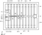
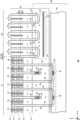
- FIG. 1 shows an example of the layout of components on the front surface of a semiconductor device 100 according to an embodiment.
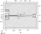
- An example of the arrangement of emitter electrodes 52 provided on the front surface of the semiconductor device 100 is shown.
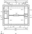
- 1 shows an example of the arrangement of a protective film 150 provided on the front surface of a semiconductor device 100.
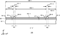
- An example of a cross section taken along line aa' of FIG. 3 is shown.
- 1 shows an example of a top view of a semiconductor device 100.
- FIG. The structure of the front surface of the semiconductor substrate 10 in the vicinity of the protection region 151-1 is shown diagrammatically.
- 8 shows an example of the bb' cross section of FIG. An example of a method for manufacturing the semiconductor device 100 will be described.
- one side in a direction parallel to the depth direction of a semiconductor substrate is referred to as the "front” or “top”, and the other side as the “back” or “bottom”.
- the top surface Of the two main surfaces of a substrate, layer, or other member, one side is referred to as the top surface, and the other side is referred to as the bottom surface.
- the directions of "front”, “top”, “back”, and “bottom” are not limited to the direction of gravity or the directions when the semiconductor device is mounted.
- the orthogonal coordinate axes merely identify the relative positions of components and do not limit a specific direction.
- the Z-axis does not limit the height direction relative to the ground.
- the +Z-axis direction and the -Z-axis direction are opposite directions.
- the Z-axis direction is written without indicating positive or negative, it means the direction parallel to the +Z-axis and -Z-axis.
- the view from the +Z-axis direction may be referred to as a top view.
- the conductivity type of the doped regions doped with impurities is described as P type or N type.
- the conductivity type of each doped region may be of the opposite polarity.
- P+ type or N+ type it means that the doping concentration is higher than P type or N type
- P- type or N- type it means that the doping concentration is lower than P type or N type.
- the doping concentration refers to the concentration of an impurity activated as a donor or acceptor.
- the difference in concentration between the donor and the acceptor may be the concentration of the greater donor or acceptor.
- the concentration difference can be measured by a voltage-capacitance measurement method (CV method).
- the carrier concentration measured by a spreading resistance measurement method (SR) may be the donor or acceptor concentration. If the donor or acceptor concentration distribution has a peak, the peak value may be the donor or acceptor concentration in that region. In cases where the donor or acceptor concentration in a region where the donor or acceptor is present is approximately uniform, the average donor or acceptor concentration in that region may be the donor or acceptor concentration.
- FIG. 1 shows an example of the arrangement of each component on the front surface of a semiconductor device 100 according to an embodiment.
- the semiconductor device 100 comprises a semiconductor substrate 10, a gate pad 50, a current sense pad 172, a temperature sense section 178, an anode pad 174 and a cathode pad 176 electrically connected to the temperature sense section 178, a bidirectional diode section 210, and an output comparison diode section 220.
- the area in which the current sense pad 172, anode pad 174, cathode pad 176, bidirectional diode section 210, and output comparison diode section 220 are provided may be collectively referred to as the pad area.
- the semiconductor substrate 10 has an edge 102.
- the direction of one edge 102-1 of the semiconductor substrate 10 in the top view of FIG. 1 is the X-axis
- the direction perpendicular to the X-axis is the Y-axis.
- the X-axis is taken in the direction of the edge 102-1.
- the direction perpendicular to the X-axis direction and the Y-axis direction, which forms a right-handed system, is referred to as the Z-axis direction.
- the temperature sensor 178 is provided in the +Z-axis direction of the semiconductor substrate 10.
- the semiconductor substrate 10 is made of a semiconductor material such as silicon or a compound semiconductor.
- the side on which the temperature sensing unit 178 is provided is referred to as the front surface, and the opposing surface is referred to as the back surface.
- the direction connecting the front surface and the back surface of the semiconductor substrate 10 is referred to as the depth direction.
- the semiconductor substrate 10 has a substantially rectangular shape on the front surface, but may have a different shape.
- the semiconductor substrate 10 has an active portion 120.
- the active portion 120 is a region in which a main current flows in the depth direction between the front and back surfaces of the semiconductor substrate 10 when the semiconductor device 100 is in an on-state.
- a gate conductive portion 44 of the active portion 120 which will be described later, is electrically connected to the gate pad 50 by a gate wiring portion, which will be described later.
- the active portion 120 may be divided into active portion 120-1 and active portion 120-2 when viewed from above.
- active portion 120-1 and active portion 120-2 are separated in the Y-axis direction by a separation portion 90 that extends in the Y-axis direction through the center Ac of the front surface of the semiconductor substrate 10.
- the center Ac of the active portion 120 is the geometric center of gravity of the active portion 120 when viewed from above.
- the active portions 120-1 and 120-2 may be arranged with a pad region between them.
- the active section 120 includes a transistor section 70 including transistor elements such as an IGBT (insulated gate bipolar transistor) and a diode section 80 including diode elements such as an FWD (freewheel diode).
- the transistor section 70 and the diode section 80 form an RC-IGBT (Reverse Conducting IGBT).
- the region in the active section 120 where the transistor section 70 is arranged is marked with the symbol "I"
- the region in which the diode section 80 is arranged is marked with the symbol "F”.
- the transistor sections 70 and diode sections 80 are arranged alternately in the X-axis direction in each region of the active section 120.
- the width of the transistor section 70 is 300 ⁇ m or more and 2000 ⁇ m or less
- the width of the diode section 80 is 200 ⁇ m or more and 2000 ⁇ m or less.
- the semiconductor device 100 has an edge termination structure on the front surface between the outer periphery of the active section 120 and the edge 102.
- the edge termination structure has, for example, a guard ring provided in an annular shape surrounding the active section 120, a field plate, or a structure that combines these.
- the temperature sensing section 178 may be disposed in the separation section 90.
- the separation section 90 does not include the active section 120.
- the center of the semiconductor substrate 10 is likely to heat up due to heat generated from the switching elements formed in the active section 120.
- the temperature sensing section 178 in the separation section 90 near the center, the temperature of the transistor section 70 can be monitored. This makes it possible to prevent the transistor section 70 from overheating beyond the junction temperature, which is within the normal operating temperature range.
- the temperature sensing unit 178 may be provided by a temperature sensing diode.
- the temperature sensing unit 178 is provided by a Schottky diode.
- the temperature sensing unit 178 may also be provided by a PN junction diode made of polycrystalline silicon provided above the semiconductor substrate 10 via an insulating film.
- the anode and cathode of the temperature sensing diode are connected to anode wiring 180 and cathode wiring 182 made of metal, respectively.
- the anode wiring 180 and cathode wiring 182 are wiring containing a metal such as aluminum.
- the anode wiring 180 and cathode wiring 182 are an example of a temperature sensing wiring.
- the anode wiring 180 and cathode wiring 182 are provided by extending the separation section 90.
- the cathode pad 176 is connected to the temperature sensor 178 via a cathode wiring 182.
- the anode pad 174 is connected to the temperature sensor 178 via an anode wiring 180.
- the cathode pad 176 and the anode pad 174 are electrodes that contain a metal such as aluminum.
- the current sense pad 172 is electrically connected to the current sense section 110.
- the current sense pad 172 is an example of a front surface electrode.
- the current sense section 110 has a structure similar to that of the transistor section 70 of the active section 120, and simulates the operation of the transistor section 70. A current proportional to the current flowing through the transistor section 70 flows through the current sense section 110. This makes it possible to monitor the current flowing through the transistor section 70.
- the current sense section 110 does not have an emitter region 12, which will be described later. In other words, the current sense section 110 does not operate as a transistor.
- the current sense section 110 has a gate trench section. The gate trench section of the current sense section 110 is electrically connected to the gate wiring section.
- the bidirectional diode section 210 is disposed between the anode pad 174 and the cathode pad 176 on the front surface of the semiconductor device 100.
- the bidirectional diode section 210 includes diodes electrically connected in series in both directions between the anode pad 174 and the cathode pad 176.
- the bidirectional diode section 210 prevents the temperature sensing section 178 from being damaged by electrostatic discharge (Electro-Static Discharge, ESD).
- the output comparison diode section 220 is provided between the anode pad 174 and the cathode pad 176.
- the output comparison diode section 220 is electrically connected to the anode pad 174 and the cathode pad 176.
- the output comparison diode section 220 includes an output comparison diode having a PN junction direction connected in anti-parallel to the PN junction direction of the temperature sense diode of the temperature sense section 178.
- the output comparison diodes of the output comparison diode section 220 may have a similar design to the diodes of the temperature sense section 178, except for the direction of the PN junction.
- no current flows through the output comparison diode section 220.
- An output comparison operation is performed at predetermined intervals. During the output comparison operation, a current flows through the output comparison diode section 220. The output comparison operation makes it possible to know when to replace the temperature sense diode of the temperature sense section 178.
- a protection diode having the same forward direction as the output comparison diode section 220 may be provided in parallel with the output comparison diode section 220.
- the protection diode prevents the application of an overvoltage or the inflow of an overcurrent to the temperature sensing section 178 due to noise or the like when the temperature sensing section 178 is in operation.
- FIG. 2 shows an example of the arrangement of emitter electrodes 52 provided on the front surface of the semiconductor device 100.
- the emitter electrodes 52 are made of a metal conductor such as aluminum.
- the emitter electrodes 52 are set to an emitter potential, which is a predetermined reference potential.
- the emitter potential may be set to a ground potential.
- the emitter electrode 52 is formed of a conductive material that contains a metal.
- the emitter electrode 52 is formed of aluminum or an alloy mainly composed of aluminum (such as an alloy of aluminum-silicon or aluminum-silicon-copper).
- the emitter electrode 52 is an example of a front surface electrode, similar to the current sense pad 172.
- Each electrode may have a barrier metal formed of titanium or a titanium compound, etc., under an area formed of aluminum, etc.
- the emitter electrode 52 is disposed in the region hatched with diagonal lines.
- the emitter electrode 52 is not provided above the separation portion 90 that separates the active portion 120-1 and the active portion 120-2 from each other in the Y-axis direction. Similarly, the emitter electrode 52 is not provided above the pad region.
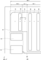
- FIG. 3 shows an example of the arrangement of a protective film 150 provided above the front surface of the semiconductor device 100.
- the protective film 150 is made of polyimide.
- the outline of the area where the protective film 150 is arranged is shown by a dashed line and hatched with diagonal lines.
- the protective film 150 may be in contact with the upper surface of the emitter electrode 52.
- the protective film 150 in this example has a protective film 150-1 that covers the region where the gate pad 50 is provided, and a protective film 150-2 that covers the pad region.
- the protective film 150-1 may have an opening that exposes a portion of the upper surface of the gate pad 50.
- the protective film 150-1 may have an opening 153 that exposes a portion of the upper surface of the current sense pad 172, and an opening 154 that exposes a portion of the upper surfaces of the anode pad 174 and the cathode pad 176.
- This allows wires and the like to be connected to the upper surface of the gate pad 50.
- wires and the like can also be connected to the upper surfaces of the current sense pad 172, the anode pad 174, and the cathode pad 176.
- the protective film 150 may further include a protective film 150-3 provided between the outer periphery of the active section 120 and the edge 102 (edges 102-1 to 102-4), and a protective film 150-4 covering the separation section 90.
- the emitter electrode 52 is divided into two regions surrounded by the protective film 150-1, the protective film 150-2, the protective film 150-3, and the protective film 150-4.
- the protective film 150 further includes protective film 150-5 and protective film 150-6 that are provided by extending the upper surface of the emitter electrode 52 in the Y-axis direction.
- protective film 150-5 is sandwiched between protective film 150-2 and protective film 150-3, and protective film 150-6 is sandwiched between protective film 150-1 and protective film 150-3.
- the protective films 150-5 and 150-6 are provided on the upper surface of the emitter electrode 52, unlike the other protective films 150 provided on the front surface of the semiconductor substrate 10. That is, of the protective films 150, only the protective films 150-5 and 150-6 are provided within the active section 120.
- the active section 120 has a protective region 151 where a protective film is provided, and an unprotected region 152 where no protective film is provided.
- the active section 120 in this example has a protective region 151-1 and a protective region 151-2 where the protective films 150-5 and 150-6 are provided, and an unprotected region 152-1, an unprotected region 152-2, and an unprotected region 152-3 where no protective film is provided.
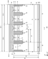
- FIG. 4 shows an example of the a-a' cross section of FIG. 3.
- the a-a' cross section is an XZ plane passing through the active section 120-1.
- the active section 120-1 in this example has an unprotected region 152-1 provided near the center when viewed from above, and unprotected regions 152-2 and 152-3 located on both sides of the unprotected region 152-1 in the X-axis direction.
- the active section 120-1 further has a protected region 151-1 sandwiched between the unprotected region 152-1 and the unprotected region 152-2, and a protected region 151-2 sandwiched between the unprotected region 152-1 and the unprotected region 152-3.
- Protective films 150-5 and 150-6 are provided on the protected region 151-1 and the protected region 151-2, respectively.
- a plating portion 161 is provided on the upper surface of the emitter electrode 52.
- plating portion 161 is Ni/Au, in which an Au layer is laminated on a Ni layer.
- Plating portion 161 is separated into plating portion 161-1, plating portion 161-2, and plating portion 161-3 by protective film 150-5 and protective film 150-6.
- Plating portion 161-1, plating portion 161-2, and plating portion 161-3 are provided in unprotected region 152-2 and unprotected region 152-3, respectively, which are located on either side of unprotected region 152-1.
- protective film 150-5 is sandwiched between plating portion 161-1 and plating portion 161-2, and protective film 150-6 is sandwiched between plating portion 161-1 and plating portion 161-3.
- Emitter electrode 52 is provided by extending below protective film 150-5 and protective film 150-6, as well as plating portion 161-1, plating portion 161-2, and plating portion 161-3.
- the width W1 of the protection area 151-1 and the width W2 of the protection area 151-2 may be the same.
- the width W1 of the protection area 151-1 and the width W2 of the protection area 151-2 are 100 ⁇ m or more and 1800 ⁇ m or less.
- the thickness D1 of the protective film 150-5 and the thickness D2 of the protective film 150-6 may be the same.
- the thickness refers to the distance in the +Z axis direction with the top surface of the emitter electrode 52 as the reference.
- the thickness D1 of the protective film 150-5 and the thickness D2 of the protective film 150-6 are greater than the thickness d1 of the plating portion 161-1 sandwiched between the protective film 150-5 and the protective film 150-6.
- the thickness D1 of the protective film 150-5 and the thickness D2 of the protective film 150-6 are 5 ⁇ m or more and 15 ⁇ m or less.
- the thickness d1 of the plating portion 161-1 is 1 ⁇ m or more and 10 ⁇ m or less.
- the area of the unprotected region 152-1 is larger than the areas of the unprotected regions 152-2 and 152-3 in a top view. Therefore, when mounting the semiconductor device 100, the emitter electrode 52 can be easily electrically connected to the outside by joining wiring such as a lead frame via a solder layer provided on the plating portion 161-1 of the unprotected region 152-1.
- protective film 150-5 and protective film 150-6 is greater than the height of plating portion 161-1, it is possible to prevent the solder layer and the like on plating portion 161-1 of non-protected region 152-1 from flowing out into non-protected region 152-2 and non-protected region 152-3.
- non-protected region 152-2 and non-protected region 152-3 are provided on opposite sides of non-protected region 152-1, it is possible to prevent the position of the solder layer and the like on the front surface of semiconductor substrate 10 from being biased.
- FIG. 4 shows the XZ plane passing through active section 120-1, but the XZ plane passing through active section 120-2 has a similar configuration, so a description thereof will be omitted here.
- FIG. 5 shows an example of a top view of the semiconductor device 100.
- FIG. 5 shows the vicinity of the negative end of the active section 120-2 in the Y-axis direction.
- the semiconductor device 100 includes a semiconductor substrate 10 having a transistor section 70 including a transistor element such as an IGBT, and a diode section 80 including a diode element such as a free wheel diode (FWD).
- a transistor section 70 including a transistor element such as an IGBT and a diode section 80 including a diode element such as a free wheel diode (FWD).
- FWD free wheel diode
- the semiconductor device 100 of this example includes a gate trench portion 40, a dummy trench portion 30, a well region 130, an emitter region 12, a base region 14, and a contact region 15 provided inside the front surface side of a semiconductor substrate 10.
- the gate trench portion 40 and the dummy trench portion 30 are each an example of a trench portion.
- the semiconductor device 100 of this example also includes a gate metal layer 48 and an emitter electrode 52 provided above the front surface of the semiconductor substrate 10.
- the gate metal layer 48 and the emitter electrode 52 are also an example of a front surface electrode.
- the gate metal layer 48 and the emitter electrode 52 are provided separately from each other.
- the gate metal layer 48 and the emitter electrode 52 are electrically insulated.
- An interlayer insulating film is provided between the emitter electrode 52 and the gate metal layer 48 and the front surface of the semiconductor substrate 10, but is omitted in FIG. 5.
- contact holes 49, 54, and 56 are provided through the interlayer insulating film. In FIG. 5, each contact hole is hatched with diagonal lines.
- the emitter electrode 52 is provided above the gate trench portion 40, the dummy trench portion 30, the well region 130, the emitter region 12, the base region 14, and the contact region 15.
- the emitter electrode 52 is electrically connected to the emitter region 12, the base region 14, and the contact region 15 on the front surface of the semiconductor substrate 10 by contact holes 54.
- the emitter electrode 52 is also connected to a dummy conductive portion in the dummy trench portion 30 by contact holes 56.
- the gate metal layer 48 may be provided in a ring shape along the outer periphery of the active portion 120. In this example, the gate metal layer 48 is provided along the outer periphery of each of the active portions 120-1 and 120-2. The gate metal layer 48 is connected to the gate conductive portion in the gate trench portion 40 by a contact hole 49.
- Front electrodes such as the emitter electrode 52 or the gate metal layer 48 are made of a conductive material that contains metal. For example, they are made of aluminum or an aluminum-silicon alloy. Each electrode may have a barrier metal made of titanium or a titanium compound under the region made of aluminum or the like.
- Each electrode may have a plug formed of tungsten or the like in the contact hole.
- the plug may have a barrier metal on the side in contact with the semiconductor substrate 10, with tungsten embedded so as to contact the barrier metal, and may be formed of aluminum or the like on the tungsten.
- the plug is provided in a contact hole that contacts the contact region 15 or the base region 14.
- a P++ type plug region having a higher doping concentration than the contact region 15 may be provided below the plug contact hole. This can improve the contact resistance between the barrier metal and the contact region 15.
- the depth of the plug region is approximately 0.1 ⁇ m or less, which is less than 10% of the depth of the contact region 15.
- the plug region improves the contact resistance, improving the latch-up resistance during operation of the transistor section 70. Meanwhile, increases in conduction loss and switching loss during operation of the diode section 80 can be suppressed.
- a connection portion 25 may further be provided to electrically connect the emitter electrode 52 or a front surface electrode such as the gate metal layer 48 to the semiconductor substrate 10.
- the connection portion 25 is provided in a region including the inside of the contact hole 49 between the gate metal layer 48 and the gate conductive portion.
- the connection portion 25 may also be provided in a region including the inside of the contact hole 56 between the emitter electrode 52 and the dummy conductive portion.
- connection portion 25 is a conductive material such as a metal such as tungsten or polysilicon doped with impurities.
- the connection portion 25 may also have a barrier metal such as titanium nitride.
- the connection portion 25 is polysilicon doped with N-type impurities (N+).
- the connection portion 25 is provided above the front surface of the semiconductor substrate 10 via an insulating film such as an oxide film.
- the well region 130 is provided on the front surface side of the semiconductor substrate 10 relative to the drift region 18 described below.
- the well region 130 is P+ type.
- the well region 130 is provided in the edge termination structure and the isolation portion 90.
- the well region 130 is provided in a predetermined range from the outer periphery to the inside of the active portion 120-1 and the active portion 120-2.
- the well region 130 is electrically connected to the emitter electrode 52.
- the well region 130 is provided from the front surface of the semiconductor substrate 10 to a position deeper than the lower end of the base region 14.
- Each of the transistor section 70 and the diode section 80 has multiple trench sections arranged in the arrangement direction.
- the transistor section 70 of this example one or more gate trench sections 40 and one or more dummy trench sections 30 are alternately provided along the arrangement direction.
- the diode section 80 of this example multiple dummy trench sections 30 are provided along the arrangement direction.
- the arrangement direction of the trench portions is the X-axis direction
- the extension direction perpendicular to the arrangement direction is the Y-axis direction.
- the gate trench portion 40 in this example may have two extension portions 39 (portions of the trench that are linear along the extension direction) that extend along the extension direction, and a connection portion 41 that connects the two extension portions 39.
- connection portion 41 may be curved when viewed from above.
- the connection portion 41 connects the ends of the two extension portions 39 in the Y-axis direction to the gate metal layer 48, and functions as a gate electrode to the gate trench portion 40.
- the connection portion 41 by making the connection portion 41 curved, electric field concentration at the ends can be alleviated more effectively than if the connection portion 41 were completed at the extension portion 39.
- the dummy trench section 30 is provided between each extension section 39 of the gate trench section 40.
- one dummy trench section 30 is provided between each extension section 39, but two or more dummy trench sections 30 may be provided.
- each extension portion 39 a dummy trench portion 30 does not have to be provided, and a gate trench portion 40 may be provided.
- the electron current from the emitter region 12 can be increased, thereby reducing the on-voltage.
- the dummy trench portion 30 may have a linear shape extending in the extension direction, and may have an extension portion 29 and a connection portion 31, similar to the gate trench portion 40.
- the semiconductor device 100 shown in FIG. 4 has only dummy trench portions 30 having connection portions 31 arranged therein, but in other examples, the semiconductor device 100 may include linear dummy trench portions 30 that do not have connection portions 31.
- the diffusion depth of the well region 130 may be deeper than the depth of the gate trench portion 40 and the dummy trench portion 30.
- the ends of the gate trench portion 40 and the dummy trench portion 30 in the Y-axis direction are provided in the well region 130 when viewed from above. In other words, at the ends of each trench portion in the Y-axis direction, the bottom of each trench portion in the depth direction (-Z-axis direction) is covered by the well region 130. This makes it possible to reduce electric field concentration at the bottom of each trench portion.
- the mesa portion refers to the region inside the semiconductor substrate 10 that is sandwiched between the trench portions.
- the depth position of the mesa portion is from the front surface of the semiconductor substrate to the bottom end of the trench portion.
- the mesa portion in this example is sandwiched between adjacent trench portions in the X-axis direction and extends in the extension direction (Y-axis direction) along the trenches on the front surface of the semiconductor substrate 10.
- Each mesa portion has a base region 14.
- at least one of an emitter region 12 and a contact region 15 may be provided in a region sandwiched between the base regions 14 when viewed from above.
- the base region 14 is P- type
- the emitter region 12 is N+ type
- the contact region 15 is P+ type.
- the base region 14 is provided in contact with the well region 130.
- the emitter region 12 and the contact region 15 may be provided between the base region 14 and the front surface of the semiconductor substrate 10 in the depth direction.
- dopants for the emitter region 12 include arsenic (As), phosphorus (P), and antimony (Sb).
- the mesa portion of the transistor section 70 has an emitter region 12 exposed on the front surface of the semiconductor substrate 10.
- the emitter region 12 is provided in contact with the gate trench portion 40.
- the mesa portion in contact with the gate trench portion 40 has a contact region 15 exposed on the front surface of the semiconductor substrate 10.
- the contact regions 15 and emitter regions 12 in the mesa portion are each provided from one trench portion to the other trench portion in the X-axis direction.
- the contact regions 15 and emitter regions 12 in the mesa portion are alternately arranged along the extension direction of the trench portion (Y-axis direction).
- the contact region 15 and emitter region 12 of the mesa portion may be provided in a stripe shape along the extension direction (Y-axis direction) of the trench portion.
- the emitter region 12 is provided in a region that contacts the trench portion, and the contact region 15 is provided in a region sandwiched between the emitter regions 12.
- the mesa portion of the diode portion 80 does not have an emitter region 12.
- a base region 14 may be provided on the upper surface of the mesa portion of the diode portion 80.
- the base region 14 may be disposed over the entire mesa portion of the diode portion 80.
- the base region 14 of the diode portion 80 acts as an anode.
- a contact hole 54 is provided above each mesa portion.
- the contact holes 54 are arranged in a region sandwiched between the base regions 14 in the extension direction (Y-axis direction). In this example, the contact holes 54 are provided above the contact region 15, the base region 14, and the emitter region 12.
- the contact holes 54 may be arranged in the center in the arrangement direction of the mesa portions (X-axis direction).
- an N+ type cathode region 82 is provided on the rear surface of the semiconductor substrate 10.
- a P+ type collector region 22 may be provided in an area where the cathode region 82 is not provided.
- the boundary between the cathode region 82 and the collector region 22 is indicated by a dashed line.
- FIG. 6 shows a schematic diagram of the structure of the front surface of the semiconductor substrate 10 near the protection region 151-1.
- the emitter electrode 52 and other elements provided above the front surface of the semiconductor substrate 10 are omitted.
- FIG. 6 shows an example of the structure near the protection region 151-1 of the active section 120-1, but the active section 120-2 has a similar structure, so a description thereof will be omitted.
- a cathode region 82 is provided on the back surface of the semiconductor substrate 10.
- the unprotected region 152-1 is provided near the center of the active section 120-1, and the unprotected region 152-2 is provided on the positive side of the pad region in the Y-axis direction, between the pad region, the protected region 151-1, and the gate metal layer 48.
- Transistor sections 70 and diode sections 80 are alternately provided in the unprotected region 152-1 and the unprotected region 152-2.
- FIG. 6 illustrates one transistor section 70 and one diode section 80 in each of the unprotected regions 152-1 and 152-2, but this is not limited to the above.
- a plurality of transistor sections 70 and diode sections 80 may be provided alternately in each of the unprotected regions 152-1 and 152-2.
- the length of the unprotected region 152-1 is greater than the length of the unprotected region 152-2.
- the unprotected region 152-2 is a region provided in a corner portion of the chip where the unprotected region 152-1 and pad region are not provided, and by extending the active portion 120-1 to such a portion, the area on the chip can be effectively utilized.
- Protected region 151-1 is sandwiched between unprotected region 152-1 and unprotected region 152-2.
- protected region 151-1 is provided with only transistor section 70, and does not have diode section 80.
- Protected region 151-1 may be provided in the center of transistor section 70.
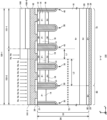
- FIG. 7 shows an example of the bb' cross section of FIG. 6.
- the bb' cross section is an XZ plane that passes through the transistor section 70 and a part of the diode section 80, and passes through the emitter region 12 in the transistor section 70.
- the semiconductor device 100 of this example has a semiconductor substrate 10, an interlayer insulating film 38, an emitter electrode 52, a protective film 150-5, a plating portion 161-2, and a collector electrode 24.
- the interlayer insulating film 38 is formed above the front surface 21 of the semiconductor substrate 10, and the emitter electrode 52 is formed above the interlayer insulating film 38.
- the drift region 18 is a region provided in the semiconductor substrate 10.
- the drift region 18 is, as an example, N-type.
- the drift region 18 may be a region remaining in the semiconductor substrate 10 without other doped regions being formed therein.
- the doping concentration of the drift region 18 may be the doping concentration of the semiconductor substrate 10.
- the buffer region 20 is a region provided below the drift region 18.
- the buffer region 20 has the same conductivity type as the drift region 18, and is, for example, N-type.
- the doping concentration of the buffer region 20 is higher than the doping concentration of the drift region 18.
- the buffer region 20 may function as a field stop layer that prevents the depletion layer spreading from the lower surface side of the base region 14 from reaching the collector region 22 and the cathode region 82.
- the collector region 22 is a region of a different conductivity type than the drift region 18, which is provided below the buffer region 20 in the transistor section 70.
- the cathode region 82 is a region of the same conductivity type as the drift region 18, which is provided below the buffer region 20 in the diode section 80.
- the boundary between the collector region 22 and the cathode region 82 is the boundary between the transistor section 70 and the diode section 80.
- the collector electrode 24 is formed on the rear surface 23 of the semiconductor substrate 10.
- the collector electrode 24 is formed of a conductive material such as a metal.
- the base region 14 is a region of a different conductivity type from the drift region 18, which is provided above the drift region 18 in the mesa portion.
- the base region 14 is P-type, for example.
- the base region 14 is provided in contact with the gate trench portion 40.
- the base region 14 may be provided in contact with the dummy trench portion 30.
- the emitter region 12 is provided between the base region 14 and the front surface 21 of the semiconductor substrate 10.
- the emitter region 12 is provided in the mesa portion of the transistor portion 70, and is not provided in the mesa portion of the diode portion 80.
- the emitter region 12 is provided in contact with the gate trench portion 40.
- the emitter region 12 may or may not be in contact with the dummy trench portion 30.
- the contact regions 15 are provided alternately with the emitter regions 12 in the mesa portion of the transistor section 70.
- the contact regions 15 may be provided to a position deeper in the semiconductor substrate 10 than the emitter regions 12.
- the accumulation region 16 is a region that is provided closer to the front surface 21 of the semiconductor substrate 10 than the drift region 18.
- the accumulation region 16 has the same conductivity type as the drift region 18, and is, for example, N+ type.
- the accumulation region 16 is provided only in the transistor section 70, but may also be provided in the diode section 80. Furthermore, the accumulation region 16 may be provided in multiple stages.
- the accumulation region 16 is provided in contact with the gate trench portion 40.
- the accumulation region 16 may or may not be in contact with the dummy trench portion 30.
- the doping concentration of the accumulation region 16 is higher than the doping concentration of the drift region 18.
- One or more gate trench portions 40 and one or more dummy trench portions 30 are provided on the front surface 21 of the semiconductor substrate 10. Each trench portion is provided from the front surface 21 of the semiconductor substrate 10 to the drift region 18. In the regions where at least one of the emitter region 12, the base region 14, the contact region 15, and the accumulation region 16 is provided, each trench portion also penetrates these regions to reach the drift region 18.
- the trench portion penetrating the doping region is not limited to being manufactured in the order of forming the doping region and then the trench portion. Forming the trench portion and then forming the doping region between the trench portions is also included in the trench portion penetrating the doping region.
- the gate trench portion 40 has a gate trench, a gate insulating film 42, and a gate conductive portion 44 formed on the front surface 21 of the semiconductor substrate 10.
- the gate insulating film 42 is provided to cover the inner wall of the gate trench.
- the gate insulating film 42 may be formed by oxidizing or nitriding the semiconductor on the inner wall of the gate trench.
- the gate conductive portion 44 is provided inside the gate trench, further inside than the gate insulating film 42.
- the gate insulating film 42 insulates the gate conductive portion 44 from the semiconductor substrate 10.
- the gate conductive portion 44 is formed of a conductive material such as polysilicon.
- the gate trench portion 40 is covered by an interlayer insulating film 38 on the front surface 21 of the semiconductor substrate 10.
- the gate conductive portion 44 includes a region that faces the adjacent base region 14 on the mesa side, across the gate insulating film 42, in the depth direction (-Z axis direction) of the semiconductor substrate 10. When a predetermined voltage is applied to the gate conductive portion 44, a channel is formed by an electron inversion layer in the surface layer of the interface of the base region 14 that contacts the gate trench.
- the dummy trench portion 30 may have the same structure as the gate trench portion 40.
- the dummy trench portion 30 has a dummy trench, a dummy insulating film 32, and a dummy conductive portion 34 formed on the front surface 21 side of the semiconductor substrate 10.
- the dummy insulating film 32 is provided to cover the inner wall of the dummy trench.
- the dummy conductive portion 34 is provided inside the dummy trench and is provided further inward than the dummy insulating film 32.
- the dummy insulating film 32 insulates the dummy conductive portion 34 from the semiconductor substrate 10.
- the dummy trench portion 30 is covered by an interlayer insulating film 38 on the front surface 21 of the semiconductor substrate 10.
- the interlayer insulating film 38 is provided on the front surface 21 of the semiconductor substrate 10.
- An emitter electrode 52 is provided above the interlayer insulating film 38.
- One or more contact holes 54 are provided in the interlayer insulating film 38 to electrically connect the emitter electrode 52 to the semiconductor substrate 10.
- Contact holes 55 and 56 may also be provided penetrating the interlayer insulating film 38.
- a lifetime control region 85 including a lifetime killer is provided in the drift region 18, extending from the diode section 80 to at least a portion of the transistor section 70.
- the lifetime control region 85 is a crystal defect formed inside the semiconductor substrate 10 by injecting helium ions or the like at a predetermined depth position.
- the lifetime control region 85 promotes recombination between holes generated in the base region 14 of the diode section 80 and the transistor section 70 and electrons injected from the cathode region 82, and promotes carrier annihilation, thereby suppressing the peak current during reverse recovery.
- the peak position of the lifetime killer concentration distribution in the Z-axis direction is indicated by an "x" symbol.
- the peak position of the lifetime killer concentration distribution may be at the same depth as the bottom end of the well region 130, or it may be deeper.
- the lifetime control region 85 may be formed to have multiple peaks of the lifetime killer concentration distribution in the Z-axis direction.
- the lifetime control region 85 in this example is formed by irradiating the front surface 21 side of the semiconductor substrate 10 with protons or helium. In one example, the lifetime control region 85 is formed by shielding the area where the lifetime control region 85 is not to be formed with a mask such as resist and irradiating with helium ions.
- the lifetime control region 85 is provided only in the non-protected region 152, and not in the protected region 151.
- the lifetime control region 85 is spaced apart from the protected region 151, and the distance L1 between the protected region 151-1 and the lifetime control region 85 in the X-axis direction is 20 ⁇ m or more and 1800 ⁇ m or less.
- helium ions are irradiated from the front surface 21 side of the semiconductor substrate 10.
- helium ions are light ions, their range changes in the protected region 151 where the protective film 150 is provided, and this causes variation in the depth direction position of the lifetime control region 85 between the protected region 151 and the unprotected region 152.
- the protected region 151 is not irradiated with helium ions, and only the unprotected region 152 is irradiated with helium ions, thereby making the depth direction position of the lifetime control region 85 uniform and promoting carrier annihilation when the diode section 80 is turned off, thereby suppressing the peak current during reverse recovery.
- the distance L2 that the lifetime control region 85 extends in the transistor portion 70 is 80% or more and 250% or less of the thickness D0 of the semiconductor substrate 10.
- the thickness D0 of the semiconductor substrate 10 refers to the distance from the front surface 21 to the back surface 23 in the depth direction (-Z-axis direction) of the semiconductor substrate 10.
- the thickness D0 of the semiconductor substrate 10 may be 50 ⁇ m or more and 150 ⁇ m or less, or may be 70 ⁇ m or more and 80 ⁇ m or less.
- the diode section 80 When the diode section 80 is in operation, carriers diffuse from the diode section 80 to the outside. In one example, the carriers move at an angle of approximately 45° from the front surface 21 of the semiconductor substrate 10 toward the back surface 23. In this example, the lifetime control region 85 is provided so as to extend into the transistor section 70 by a distance L2, thereby making it possible to capture the carriers that have diffused from the diode section 80.
- the distance between the protective region 151-1 and the diode section 80 in the X-axis direction is equal to or greater than the thickness D0 of the semiconductor substrate 10.
- the protective film 150 is formed by over-etching polyimide, but there is a large variation in the finished position. Therefore, by providing a margin, it is possible to suppress the effect on performance even if variation occurs.
- the protective region 151 in this example is provided inside the transistor section 70, separated from the diode section 80 and the lifetime control region 85. This allows the lifetime control region 85 to be provided without being affected by the protective film 150, and by promoting carrier annihilation when the diode section 80 is turned off, the peak current during reverse recovery can be suppressed.
- FIG. 8 shows an example of a method for manufacturing the semiconductor device 100.
- the process for forming the lifetime control region 85 will be mainly described in the method for manufacturing the semiconductor device 100, using the same cross section b-b' of FIG. 6 as FIG. 7 as an example.
- the manufacturing method of the semiconductor device 100 of this example includes the steps of forming an active section 120 (plated active section 120-1 in FIG. 8) in which transistor sections 70 and diode sections 80 are alternately arranged in the semiconductor substrate 10, forming a plurality of trench sections (gate trench sections 40 and dummy trench sections 30 in FIG. 8) in the semiconductor substrate 10, and forming an emitter electrode 52 above the front surface 21 of the semiconductor substrate 10.
- the step of forming the active portion 120 includes a step of injecting dopants into the semiconductor substrate 10 to form impurity-injected regions such as the emitter region 12, the base region 14, the contact region 15, and the accumulation region 16.
- the step of forming the multiple trench portions includes a step of forming trenches by etching the front surface 21 of the semiconductor substrate 10, oxidizing or nitriding the semiconductor on the inner wall of the trench to form an insulating film (gate insulating film 42 and dummy insulating film 32 in FIG. 8), and filling the inside of the insulating film with a conductive material such as polysilicon to form a conductive portion (gate conductive portion 44 and dummy conductive portion 34 in FIG. 8). Either the step of forming the active portion 120 or the step of forming the multiple trench portions may be performed first.
- the stage of forming the emitter electrode 52 includes forming an interlayer insulating film 38 of BPSG or the like above the front surface 21 of the semiconductor substrate 10, etching the interlayer insulating film 38 to form contact holes, and then depositing a film of aluminum or an alloy containing aluminum as a main component (e.g., an aluminum-silicon alloy, an aluminum-silicon-copper alloy, etc.) on the front surface 21 of the semiconductor substrate 10 and the interlayer insulating film 38.
- a film of aluminum or an alloy containing aluminum as a main component e.g., an aluminum-silicon alloy, an aluminum-silicon-copper alloy, etc.
- the method for manufacturing the semiconductor device 100 further includes a step of forming a polyimide protective film 150 (protective film 150-5 in FIG. 8) on the upper surface of the emitter electrode 52. After the polyimide applied to the front surface 21 of the semiconductor substrate 10 is spin-coated and cured, the polyimide in the non-protected region 152 (non-protected region 152-2 in FIG. 8) is removed, so that the protective film 150 is formed in the protected region 151 (protected region 151-1 in FIG. 8).
- a plated portion 161 (plated portion 161-2 in FIG. 8) may be formed on the upper surface of the emitter electrode 52.
- plated portion 161 is a Ni/Au film in which an Au film for oxidation prevention is grown by immersion on a Ni film formed by electroless plating.
- the diode section 80 is included in the non-protected region 152, and the protected region 151 is included in the transistor section 70.
- the distance between the diode section 80 and the protected region 151 is equal to or greater than the thickness D0 of the semiconductor substrate 10.
- the thickness of the semiconductor substrate 10 may be equal to or greater than 50 ⁇ m and equal to or less than 150 ⁇ m, or may be equal to or greater than 70 ⁇ m and equal to or less than 80 ⁇ m.
- the method for manufacturing the semiconductor device 100 further includes a step of forming a lifetime control region 85 in the diode section 80 by irradiating a lifetime killer from the front surface 21 side of the semiconductor substrate 10.
- the lifetime killer is helium or protons.
- helium ions are irradiated through resist 190 arranged above protective film 150.
- the width of resist 190 is greater than the width of protective film 150, and resist 190 is arranged to cover at least the entire protective film 150 when viewed from above.
- the distance L1 between the end of the resist 190 and the end of the protective film 150 is 0 ⁇ m or more and 1800 ⁇ m or less.
- the end of the resist 190 may coincide with the end of the lifetime control region 85.
- the resist 190 is disposed in the transistor section 70 at a distance from the diode section 80. In the X-axis arrangement direction, the distance between the diode section 80 and the resist 190 is 80% or more and 250% or less of the thickness D0 of the semiconductor substrate 10. After the lifetime control region 85 is formed, the resist 190 is removed by a developer.
- the protective region 151 is formed inside the transistor section 70, separated from the diode section 80 and the lifetime control region 85. This allows the lifetime control region 85 to be formed without being affected by the protective film 150, and by promoting carrier annihilation when the diode section 80 is turned off, the peak current during reverse recovery can be suppressed.
Landscapes
- Semiconductor Integrated Circuits (AREA)
- Bipolar Transistors (AREA)
- Electrodes Of Semiconductors (AREA)
- Metal-Oxide And Bipolar Metal-Oxide Semiconductor Integrated Circuits (AREA)
Abstract
Description
[先行技術文献]
[特許文献]
[特許文献1] 特開2017-135339号公報
[特許文献2] 特開2009-38140号公報
Claims (18)
- トランジスタ部およびダイオード部が交互に設けられた活性部を有し、前記トランジスタ部および前記ダイオード部の延伸方向に延伸する複数のトレンチ部が設けられた半導体基板と、
前記半導体基板のおもて面の上方に設けられたエミッタ電極と、
前記エミッタ電極の上面に設けられたポリイミドの保護膜と、
を備え、
前記ダイオード部は、前記半導体基板のおもて面側から照射されたライフタイムキラーを含むライフタイム制御領域を有し、
前記活性部は、前記保護膜が設けられた保護領域と、前記保護膜が設けられていない非保護領域とを有し、
前記ダイオード部は前記非保護領域に含まれ、前記保護領域は前記トランジスタ部に含まれている
半導体装置。 - トレンチ配列方向において、前記トランジスタ部の幅は、300μm以上、2000μm以下である
請求項1に記載の半導体装置。 - トレンチ配列方向において、前記ダイオード部の幅は、200μm以上、2000μm以下である
請求項1に記載の半導体装置。 - トレンチ配列方向において、前記保護領域の幅は、100μm以上、1800μm以下である
請求項1に記載の半導体装置。 - トレンチ配列方向において、前記保護領域と前記ダイオード部との間の距離は、前記半導体基板の厚さ以上である
請求項1に記載の半導体装置。 - 前記ライフタイム制御領域は、トレンチ配列方向において、前記ダイオード部から前記トランジスタ部の少なくとも一部に延伸して設けられており、
トレンチ配列方向において、前記ライフタイム制御領域が前記トランジスタ部で延伸する距離は、前記半導体基板の厚さの80%以上、250%以下である
請求項1に記載の半導体装置。 - 前記半導体基板の厚さは、50μm以上、150μm以下である
請求項5または6に記載の半導体装置。 - 前記ライフタイム制御領域は、前記非保護領域のみに設けられており、
トレンチ配列方向において、前記保護領域と前記ライフタイム制御領域との間の距離は、20μm以上、1800μm以下である
請求項1に記載の半導体装置。 - 前記エミッタ電極の上面に設けられ、前記保護膜を間に挟む第1めっき部および第2めっき部をさらに備え、
前記エミッタ電極は、前記保護膜、前記第1めっき部および前記第2めっき部の下方を延伸して設けられている
請求項1に記載の半導体装置。 - 前記保護膜は、前記第1めっき部を間に挟む第1保護膜および第2保護膜を有し、
前記第1保護膜および前記第2保護膜の厚さは、前記第1めっき部の厚さよりも大きい
請求項9に記載の半導体装置。 - 前記非保護領域は、第1非保護領域および第2非保護領域を有し、前記保護領域は、前記第1非保護領域と前記第2非保護領域との間に挟まれている
請求項1に記載の半導体装置。 - 半導体基板にトランジスタ部およびダイオード部が交互に設けられた活性部を形成する段階と、
前記半導体基板に、前記トランジスタ部および前記ダイオード部の延伸方向に延伸する複数のトレンチ部を形成する段階と、
前記半導体基板のおもて面の上方にエミッタ電極を形成する段階と、
前記エミッタ電極の上面にポリイミドの保護膜を形成する段階と、
前記ダイオード部において、前記半導体基板のおもて面側からライフタイムキラーを照射してライフタイム制御領域を形成する段階と、
を備え、
前記活性部は、上面視で、前記保護膜が設けられた保護領域と、前記保護膜が設けられていない非保護領域とを有し、
前記ダイオード部は前記非保護領域に含まれ、前記保護領域は前記トランジスタ部に含まれている
半導体装置の製造方法。 - 前記ライフタイムキラーは、前記保護膜の上方に配置されたレジストを介して照射され、
トレンチ配列方向において、前記レジストの幅は、前記保護膜の幅よりも大きい
請求項12に記載の半導体装置の製造方法。 - 前記レジストは、上面視で、前記保護膜の全体を少なくとも覆って配置される
請求項13に記載の半導体装置の製造方法。 - トレンチ配列方向において、前記レジストの端部と前記保護膜の端部との間の距離は、0μm以上、1800μm以下である
請求項14に記載の半導体装置の製造方法。 - 前記レジストは、前記ダイオード部から離間して前記トランジスタ部に配置され、
トレンチ配列方向において、前記ダイオード部と前記レジストとの間の距離は、前記半導体基板の厚さの80%以上、250%以下である
請求項13に記載の半導体装置の製造方法。 - トレンチ配列方向において、前記ダイオード部と前記保護領域との間の距離は、前記半導体基板の厚さ以上である
請求項13に記載の半導体装置の製造方法。 - 前記半導体基板の厚さは、50μm以上、150μm以下である
請求項16または17に記載の半導体装置の製造方法。
Priority Applications (4)
| Application Number | Priority Date | Filing Date | Title |
|---|---|---|---|
| DE112023000796.9T DE112023000796T5 (de) | 2022-10-13 | 2023-08-24 | Halbleiterbauelement und verfahren zum herstellen eines halbleiterbauelements |
| CN202380029520.2A CN119213568A (zh) | 2022-10-13 | 2023-08-24 | 半导体装置及半导体装置的制造方法 |
| JP2024551268A JPWO2024080002A1 (ja) | 2022-10-13 | 2023-08-24 | |
| US18/896,890 US20250022710A1 (en) | 2022-10-13 | 2024-09-26 | Semiconductor device and method of manufacturing semiconductor device |
Applications Claiming Priority (2)
| Application Number | Priority Date | Filing Date | Title |
|---|---|---|---|
| JP2022-164444 | 2022-10-13 | ||
| JP2022164444 | 2022-10-13 |
Related Child Applications (1)
| Application Number | Title | Priority Date | Filing Date |
|---|---|---|---|
| US18/896,890 Continuation US20250022710A1 (en) | 2022-10-13 | 2024-09-26 | Semiconductor device and method of manufacturing semiconductor device |
Publications (1)
| Publication Number | Publication Date |
|---|---|
| WO2024080002A1 true WO2024080002A1 (ja) | 2024-04-18 |
Family
ID=90669382
Family Applications (1)
| Application Number | Title | Priority Date | Filing Date |
|---|---|---|---|
| PCT/JP2023/030566 Ceased WO2024080002A1 (ja) | 2022-10-13 | 2023-08-24 | 半導体装置および半導体装置の製造方法 |
Country Status (5)
| Country | Link |
|---|---|
| US (1) | US20250022710A1 (ja) |
| JP (1) | JPWO2024080002A1 (ja) |
| CN (1) | CN119213568A (ja) |
| DE (1) | DE112023000796T5 (ja) |
| WO (1) | WO2024080002A1 (ja) |
Cited By (1)
| Publication number | Priority date | Publication date | Assignee | Title |
|---|---|---|---|---|
| WO2025258305A1 (ja) * | 2024-06-13 | 2025-12-18 | 富士電機株式会社 | 半導体装置および半導体装置の製造方法 |
Citations (2)
| Publication number | Priority date | Publication date | Assignee | Title |
|---|---|---|---|---|
| WO2019116696A1 (ja) * | 2017-12-14 | 2019-06-20 | 富士電機株式会社 | 半導体装置 |
| WO2020162012A1 (ja) * | 2019-02-07 | 2020-08-13 | 富士電機株式会社 | 半導体装置および半導体モジュール |
Family Cites Families (2)
| Publication number | Priority date | Publication date | Assignee | Title |
|---|---|---|---|---|
| JP2009038140A (ja) | 2007-07-31 | 2009-02-19 | Panasonic Corp | 半導体装置およびその製造方法 |
| JP6676988B2 (ja) | 2016-01-29 | 2020-04-08 | 株式会社デンソー | 半導体装置 |
-
2023
- 2023-08-24 WO PCT/JP2023/030566 patent/WO2024080002A1/ja not_active Ceased
- 2023-08-24 CN CN202380029520.2A patent/CN119213568A/zh active Pending
- 2023-08-24 DE DE112023000796.9T patent/DE112023000796T5/de active Pending
- 2023-08-24 JP JP2024551268A patent/JPWO2024080002A1/ja active Pending
-
2024
- 2024-09-26 US US18/896,890 patent/US20250022710A1/en active Pending
Patent Citations (2)
| Publication number | Priority date | Publication date | Assignee | Title |
|---|---|---|---|---|
| WO2019116696A1 (ja) * | 2017-12-14 | 2019-06-20 | 富士電機株式会社 | 半導体装置 |
| WO2020162012A1 (ja) * | 2019-02-07 | 2020-08-13 | 富士電機株式会社 | 半導体装置および半導体モジュール |
Cited By (1)
| Publication number | Priority date | Publication date | Assignee | Title |
|---|---|---|---|---|
| WO2025258305A1 (ja) * | 2024-06-13 | 2025-12-18 | 富士電機株式会社 | 半導体装置および半導体装置の製造方法 |
Also Published As
| Publication number | Publication date |
|---|---|
| DE112023000796T5 (de) | 2024-11-14 |
| CN119213568A (zh) | 2024-12-27 |
| JPWO2024080002A1 (ja) | 2024-04-18 |
| US20250022710A1 (en) | 2025-01-16 |
Similar Documents
| Publication | Publication Date | Title |
|---|---|---|
| JP7556416B2 (ja) | 半導体装置 | |
| CN111146197B (zh) | 半导体装置及制造方法 | |
| US10121866B2 (en) | Semiconductor device | |
| JP7758079B2 (ja) | 半導体装置 | |
| JP7243845B2 (ja) | 半導体装置 | |
| CN113287201B (zh) | 半导体装置 | |
| JP7173172B2 (ja) | 半導体装置および半導体モジュール | |
| JP7456113B2 (ja) | 半導体装置 | |
| US12568637B2 (en) | Semiconductor device having a temperature sensor, a transistor, and a diode | |
| JP7613502B2 (ja) | 半導体装置 | |
| JP7231065B2 (ja) | 半導体装置 | |
| JP7691809B2 (ja) | 半導体装置および半導体装置の製造方法 | |
| CN112543993B (zh) | 半导体装置 | |
| US12288787B2 (en) | Semiconductor device | |
| WO2024080002A1 (ja) | 半導体装置および半導体装置の製造方法 | |
| JP7703881B2 (ja) | 半導体装置 | |
| JP7231064B2 (ja) | 半導体装置 | |
| JP7848896B2 (ja) | 半導体装置および半導体モジュール | |
| US20240332173A1 (en) | Semiconductor device | |
| WO2025258305A1 (ja) | 半導体装置および半導体装置の製造方法 | |
| WO2024262142A1 (ja) | 半導体装置および半導体装置の製造方法 | |
| JPWO2024135114A5 (ja) |
Legal Events
| Date | Code | Title | Description |
|---|---|---|---|
| 121 | Ep: the epo has been informed by wipo that ep was designated in this application |
Ref document number: 23877010 Country of ref document: EP Kind code of ref document: A1 |
|
| WWE | Wipo information: entry into national phase |
Ref document number: 202380029520.2 Country of ref document: CN |
|
| WWE | Wipo information: entry into national phase |
Ref document number: 112023000796 Country of ref document: DE |
|
| WWE | Wipo information: entry into national phase |
Ref document number: 2024551268 Country of ref document: JP |
|
| WWP | Wipo information: published in national office |
Ref document number: 202380029520.2 Country of ref document: CN |
|
| 122 | Ep: pct application non-entry in european phase |
Ref document number: 23877010 Country of ref document: EP Kind code of ref document: A1 |