WO2024079980A1 - 半導体装置、発光装置、車両 - Google Patents
半導体装置、発光装置、車両 Download PDFInfo
- Publication number
- WO2024079980A1 WO2024079980A1 PCT/JP2023/029700 JP2023029700W WO2024079980A1 WO 2024079980 A1 WO2024079980 A1 WO 2024079980A1 JP 2023029700 W JP2023029700 W JP 2023029700W WO 2024079980 A1 WO2024079980 A1 WO 2024079980A1
- Authority
- WO
- WIPO (PCT)
- Prior art keywords
- light
- switch element
- current source
- semiconductor device
- emitting element
- Prior art date
- Legal status (The legal status is an assumption and is not a legal conclusion. Google has not performed a legal analysis and makes no representation as to the accuracy of the status listed.)
- Ceased
Links
Images






Classifications
-
- B—PERFORMING OPERATIONS; TRANSPORTING
- B60—VEHICLES IN GENERAL
- B60Q—ARRANGEMENT OF SIGNALLING OR LIGHTING DEVICES, THE MOUNTING OR SUPPORTING THEREOF OR CIRCUITS THEREFOR, FOR VEHICLES IN GENERAL
- B60Q11/00—Arrangement of monitoring devices for devices provided for in groups B60Q1/00 - B60Q9/00
-
- H—ELECTRICITY
- H05—ELECTRIC TECHNIQUES NOT OTHERWISE PROVIDED FOR
- H05B—ELECTRIC HEATING; ELECTRIC LIGHT SOURCES NOT OTHERWISE PROVIDED FOR; CIRCUIT ARRANGEMENTS FOR ELECTRIC LIGHT SOURCES, IN GENERAL
- H05B45/00—Circuit arrangements for operating light-emitting diodes [LED]
- H05B45/10—Controlling the intensity of the light
- H05B45/14—Controlling the intensity of the light using electrical feedback from LEDs or from LED modules
-
- H—ELECTRICITY
- H05—ELECTRIC TECHNIQUES NOT OTHERWISE PROVIDED FOR
- H05B—ELECTRIC HEATING; ELECTRIC LIGHT SOURCES NOT OTHERWISE PROVIDED FOR; CIRCUIT ARRANGEMENTS FOR ELECTRIC LIGHT SOURCES, IN GENERAL
- H05B45/00—Circuit arrangements for operating light-emitting diodes [LED]
- H05B45/30—Driver circuits
- H05B45/32—Pulse-control circuits
- H05B45/325—Pulse-width modulation [PWM]
-
- H—ELECTRICITY
- H05—ELECTRIC TECHNIQUES NOT OTHERWISE PROVIDED FOR
- H05B—ELECTRIC HEATING; ELECTRIC LIGHT SOURCES NOT OTHERWISE PROVIDED FOR; CIRCUIT ARRANGEMENTS FOR ELECTRIC LIGHT SOURCES, IN GENERAL
- H05B45/00—Circuit arrangements for operating light-emitting diodes [LED]
- H05B45/40—Details of LED load circuits
- H05B45/44—Details of LED load circuits with an active control inside an LED matrix
-
- H—ELECTRICITY
- H05—ELECTRIC TECHNIQUES NOT OTHERWISE PROVIDED FOR
- H05B—ELECTRIC HEATING; ELECTRIC LIGHT SOURCES NOT OTHERWISE PROVIDED FOR; CIRCUIT ARRANGEMENTS FOR ELECTRIC LIGHT SOURCES, IN GENERAL
- H05B45/00—Circuit arrangements for operating light-emitting diodes [LED]
- H05B45/50—Circuit arrangements for operating light-emitting diodes [LED] responsive to malfunctions or undesirable behaviour of LEDs; responsive to LED life; Protective circuits
- H05B45/54—Circuit arrangements for operating light-emitting diodes [LED] responsive to malfunctions or undesirable behaviour of LEDs; responsive to LED life; Protective circuits in a series array of LEDs
-
- H—ELECTRICITY
- H05—ELECTRIC TECHNIQUES NOT OTHERWISE PROVIDED FOR
- H05B—ELECTRIC HEATING; ELECTRIC LIGHT SOURCES NOT OTHERWISE PROVIDED FOR; CIRCUIT ARRANGEMENTS FOR ELECTRIC LIGHT SOURCES, IN GENERAL
- H05B47/00—Circuit arrangements for operating light sources in general, i.e. where the type of light source is not relevant
- H05B47/10—Controlling the light source
- H05B47/105—Controlling the light source in response to determined parameters
-
- H—ELECTRICITY
- H05—ELECTRIC TECHNIQUES NOT OTHERWISE PROVIDED FOR
- H05B—ELECTRIC HEATING; ELECTRIC LIGHT SOURCES NOT OTHERWISE PROVIDED FOR; CIRCUIT ARRANGEMENTS FOR ELECTRIC LIGHT SOURCES, IN GENERAL
- H05B47/00—Circuit arrangements for operating light sources in general, i.e. where the type of light source is not relevant
- H05B47/10—Controlling the light source
- H05B47/16—Controlling the light source by timing means
-
- H—ELECTRICITY
- H05—ELECTRIC TECHNIQUES NOT OTHERWISE PROVIDED FOR
- H05B—ELECTRIC HEATING; ELECTRIC LIGHT SOURCES NOT OTHERWISE PROVIDED FOR; CIRCUIT ARRANGEMENTS FOR ELECTRIC LIGHT SOURCES, IN GENERAL
- H05B47/00—Circuit arrangements for operating light sources in general, i.e. where the type of light source is not relevant
- H05B47/20—Responsive to malfunctions or to light source life; for protection
- H05B47/23—Responsive to malfunctions or to light source life; for protection of two or more light sources connected in series
-
- H—ELECTRICITY
- H05—ELECTRIC TECHNIQUES NOT OTHERWISE PROVIDED FOR
- H05B—ELECTRIC HEATING; ELECTRIC LIGHT SOURCES NOT OTHERWISE PROVIDED FOR; CIRCUIT ARRANGEMENTS FOR ELECTRIC LIGHT SOURCES, IN GENERAL
- H05B47/00—Circuit arrangements for operating light sources in general, i.e. where the type of light source is not relevant
- H05B47/20—Responsive to malfunctions or to light source life; for protection
- H05B47/25—Circuit arrangements for protecting against overcurrent
Definitions
- This disclosure relates to a semiconductor device, and a light-emitting device and vehicle using the same.
- Semiconductor devices e.g., matrix switch ICs [integrated circuits] or bypass switch ICs
- matrix switch ICs integrated circuits
- bypass switch ICs bypass switch ICs
- LEDs light emitting diodes
- Patent Document 1 As an example of related prior art, Patent Document 1 can be mentioned.
- the semiconductor device disclosed in this specification includes a switch element configured to be connected in parallel to a light-emitting element, a detection circuit configured to generate a detection signal by comparing the voltage across the switch element with a predetermined threshold voltage, and a fault diagnosis circuit configured to diagnose whether the switch element is stuck off by monitoring the detection signal when the drive signal for the switch element is at an on-logic level.
- the semiconductor device disclosed in this specification includes a switch element or a current source configured to be connected in series to a light-emitting element, a detection circuit configured to generate a detection signal by comparing the voltage across the switch element or the current source with a predetermined threshold voltage, and a fault diagnosis circuit configured to diagnose whether the switch element or the current source is stuck on by monitoring the detection signal at a timing when the drive signal for the switch element or the current source is at an off logic level.
- the semiconductor device disclosed in this specification includes a switch element or a current source configured to be connected in series with a light-emitting element, a detection circuit configured to detect a drive current flowing through the switch element or the current source, and a fault diagnosis circuit configured to diagnose whether the switch element or the current source is stuck on by monitoring the detection signal when the drive signal of the switch element or the current source is at an off-logic level, and to diagnose whether the switch element or the current source is stuck off by monitoring the detection signal when the drive signal of the switch element or the current source is at an on-logic level.
- This disclosure makes it possible to provide a semiconductor device that can increase the fault detection rate, as well as a light-emitting device and a vehicle that use the same.
- FIG. 1 is a diagram showing a first configuration example of a light emitting device.
- FIG. 2 is a diagram showing a first embodiment of a semiconductor device.
- FIG. 3 is a diagram showing a first example of fault diagnosis (normal state).
- FIG. 4 is a diagram showing a second example of fault diagnosis (when an LED is short-circuited).
- FIG. 5 is a diagram showing a third example of the fault diagnosis (when the SW is stuck on).
- FIG. 6 is a diagram showing a fourth example of the fault diagnosis (when the SW is stuck in the off position).
- FIG. 7 is a diagram showing a second configuration example of the light emitting device.
- FIG. 8 is a diagram showing a second embodiment of the semiconductor device.
- FIG. 9 is a diagram showing a fifth example of fault diagnosis (normal state).
- FIG. 10 is a diagram showing a sixth example of fault diagnosis (when an LED is short-circuited).
- FIG. 11 is a diagram showing a seventh example of fault diagnosis (when an LED is open).
- FIG. 12 is a diagram showing an eighth example of the fault diagnosis (when CS is stuck on).
- FIG. 13 is a diagram showing a ninth example of the fault diagnosis (when CS is stuck in the off state).
- FIG. 14 is a diagram showing a third embodiment of the semiconductor device.
- FIG. 15 is a diagram showing a tenth example of fault diagnosis (normal state).
- FIG. 16 is a diagram showing an eleventh example of fault diagnosis (when CS is stuck on).
- FIG. 17 is a diagram showing a twelfth example of fault diagnosis (when CS is stuck in the off state).
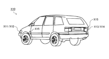
- FIG. 18 is a diagram showing the external appearance (front) of a vehicle on which a light emitting device can be mounted.
- FIG. 19 is a diagram showing the external appearance (rear view) of
- ⁇ Light-emitting device (first configuration example)> 1 is a diagram showing a first configuration example of a light emitting device.
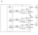
- the light emitting device 100 of this configuration example includes a semiconductor device 1 and light emitting elements 2(0) to 2(7).
- the light emitting device 100 may be, for example, a head lamp, a tail lamp, a stop lamp, a turn lamp, or an interior lamp (such as an instrument panel lamp) of a vehicle.
- the semiconductor device 1 is a matrix switch IC (bypass switch IC) that switches between short-circuiting and non-shorting each of the light-emitting elements 2(0) to 2(7).
- the semiconductor device 1 also has multiple external terminals (external terminals CH(0) to CH(8) in this figure) as means for establishing electrical connections with the outside of the device.
- Each of the light-emitting elements 2(0) to 2(7) is a series light-emitting element provided on a current path through which the drive current ILED flows.
- each can be understood as a single LED element, or as a light-emitting element assembly in which multiple LED elements are combined in series or in parallel.
- the anode of light-emitting element 2(n) is connected to external terminal CH(n+1) of semiconductor device 1.
- the light emitting device 100 may also include a semiconductor device (a so-called LED driver IC) that generates the above-mentioned drive current ILED.
- a semiconductor device a so-called LED driver IC
- the semiconductor device 1 of this configuration example includes a switch circuit 10 and a control circuit 20 built therein.
- the switch circuit 10 includes switch elements 11(0)-11(7) (in this diagram, NMOSFETs [N-channel type metal oxide semiconductor field effect transistors]), drivers 12(0)-12(7), detection circuits 13(0)-13(7), and level shifters 14(0)-14(7).
- the control circuit 20 also includes PWM [pulse width modulation] dimmer circuits 21(0)-21(7).
- the switch element 11(n) connected in this manner is in an on state when the drive signal VG(n) is at a high level, and in an off state when the drive signal VG(n) is at a low level.
- the driver 12(n) generates the drive signal VG(n) in response to the control signal S4(n) output from the PWM dimming circuit 21(n) (more precisely, the level-shifted control signal S5(n) output from the level shifter 14(n)). For example, the driver 12(n) sets the drive signal VG(n) to a high level when the control signal S4(n) is at a high level, and sets the drive signal VG(n) to a low level when the control signal S4(n) is at a low level.
- the driver 12(n) also has the function of forcibly fixing the logical level of the drive signal VG(n) in response to the detection signal S2(n) output from the detection circuit 13(n).
- Detection circuit 13(n) monitors the voltage across switch element 11(n) and generates detection signals S1(n) and S2(n).
- the voltage across switch element 11(n) is detected as a differential voltage V(n+1)-V(n) between the node voltage V(n) appearing at external terminal CH(n) and the node voltage V(n+1) appearing at external terminal CH(n+1).
- detection signals S1(n) and S2(n) may be the same signal.
- the level shifter 14(n) is provided between the control circuit 20 and the driver 12(n) and detection circuit 13(n).
- the level shifter 14(n) generates a level-shifted control signal S5(n) by shifting the signal level of the control signal S4(n) output from the PWM dimming circuit 21(n).
- the level shifter 14(n) then outputs the level-shifted control signal S5(n) to the driver 12(n).
- the level shifter 14(n) also shifts the signal level of the detection signal S1(n) output from the detection circuit 13(n) to generate a level-shifted detection signal S3(n).
- the level shifter 14(n) then outputs the level-shifted detection signal S3(n) to the control circuit 20.
- the fault detection rate of the semiconductor device 1 is calculated by dividing the element area by the number of elements. Therefore, for example, if a fault in the switch element 11(n), which has a large element area, cannot be detected, a single point fault will occur, and the fault detection rate of the semiconductor device 1 will be significantly reduced.
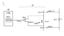
- First Embodiment 2 is a diagram showing a first embodiment (particularly, a group of components related to fault diagnosis) of the semiconductor device 1.
- a hysteresis comparator is used as the aforementioned detection circuit 13(n).
- the non-inverting input terminal (+) of detection circuit 13(n) is supplied with an added voltage V(n)+Vth(n) obtained by adding the node voltage V(n) appearing at external terminal CH(n) and the threshold voltage Vth(n).
- the inverting input terminal (-) of detection circuit 13(n) is supplied with the node voltage V(n+1) appearing at external terminal CH(n+1).
- the detection signal S1(n) is at a low level when V(n+1)>V(n)+Vth(n) and is at a high level when V(n+1)>V(n)+Vth(n). In other words, the detection signal S1(n) is at a low level when V(n+1)-V(n)>Vth(n) and is at a high level when V(n+1)-V(n) ⁇ Vth(n).
- the detection circuit 13(n) generates the detection signal S1(n) by comparing the voltage V(n+1)-V(n) across the switch element 11(n) with a predetermined threshold voltage Vth(n).
- the threshold voltage Vth(n) is set to a voltage value lower than the forward drop voltage Vf of the light-emitting element 2(n), for example.
- control circuit 20 further includes a fault diagnosis circuit 22(n).
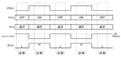
- ⁇ Fault Diagnosis (First Embodiment)> 3 is a diagram showing a first example of fault diagnosis (normal in the first embodiment).
- the drive signal VG(n) the on/off state of the switch element 11(n), the on/off state of the light-emitting element 2(n), the voltage V(n+1)-V(n) across the switch element 11(n), and the detection signal S1(n) are depicted.
- the detection signal S1(n) is at a low level.
- the fault diagnosis circuit 22(n) diagnoses that both the light-emitting element 2(n) and the switch element 11(n) are normal.
- FIG. 4 is a diagram showing a second example of fault diagnosis (when the LED is short-circuited in the first embodiment). As with FIG. 3, this diagram depicts, from top to bottom, the drive signal VG(n), the on/off state of the switch element 11(n), the on/off state of the light-emitting element 2(n), the voltage V(n+1)-V(n) across the switch element 11(n), and the detection signal S1(n).
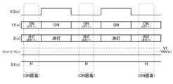
- FIG. 5 is a diagram showing a third example of fault diagnosis (when SW is stuck on in the first embodiment). As with the above-mentioned FIGS. 3 and 4, this diagram depicts, from top to bottom, the drive signal VG(n), the on/off state of the switch element 11(n), the on/off state of the light-emitting element 2(n), the voltage V(n+1)-V(n) across the switch element 11(n), and the detection signal S1(n).
- the fault diagnosis circuit 22(n) diagnoses that a short circuit has occurred in the light-emitting element 2(n) ( Figure 4) or that the switch element 11(n) is stuck on ( Figure 5).
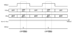
- FIG. 6 is a diagram showing a fourth example of fault diagnosis (when SW is stuck off in the first embodiment). As with FIGS. 3 to 5, from top to bottom, this diagram depicts the drive signal VG(n), the on/off state of switch element 11(n), the on/off state of light-emitting element 2(n), the voltage V(n+1)-V(n) across switch element 11(n), and the detection signal S1(n).
- the fault diagnosis circuit 22(n) diagnoses that the switch element 11(n) is stuck off when the detection signal S1(n) is at a low level while the drive signal VG(n) is at a high level.
- the fault diagnosis circuit 22(n) can diagnose not only the short circuit of the light-emitting element 2(n) but also whether the switch element 11(n) is stuck on or stuck off.
- the fault detection rate of the semiconductor device 1 is calculated by dividing the element area by the number of elements. Therefore, if a fault in the switch element 11(n), which has a large element area, can be detected, the fault detection rate of the semiconductor device 1 will be significantly improved.
- the conventional LED short detection circuit can be used as is. Therefore, the circuit scale of the semiconductor device 1 does not become unnecessarily large.
- Fault diagnosis circuit 22(n) may output the fault diagnosis result to the outside of semiconductor device 1.
- the fault diagnosis result may be a flag output, or may be read out as register data.
- the host e.g., ECU [electronic control unit]
- the host that receives the fault diagnosis result from the semiconductor device 1 can transition the light emitting device 100 to a safe state in accordance with the fault diagnosis result.
- one possible method for achieving functional safety of the light emitting device 100 is to notify the driver of the occurrence of a fault, for example, by stopping the drive current ILED and turning off all the light emitting elements 2(0) to 2(7).
- Fault diagnosis circuit 22(n) may also transition semiconductor device 1 to a safe state on its own in response to the fault diagnosis result, without waiting for control from the host.
- a possible method for achieving functional safety of semiconductor device 1 is to notify the driver of the occurrence of a fault by, for example, turning all switch elements 11(0)-11(7) on and off in a manner different from normal (all on, all off, blinking or sequential lighting, etc.).
- ⁇ Light-emitting device (second configuration example)> 7 is a diagram showing a second configuration example of a light emitting device.
- the light emitting device 100 of this configuration example includes a semiconductor device 1 and light emitting elements 2(0) to 2(7).
- the cathode of light emitting element 2(n) is connected to an external terminal CH(n) of the semiconductor device 1.
- the anodes of light emitting element 2(n) are all connected to a power supply circuit (not shown). That is, the light emitting elements 2(0) to 2(7) are connected in parallel to the power supply circuit (not shown).
- the semiconductor device 1 includes a switch circuit 10 and a control circuit 20.
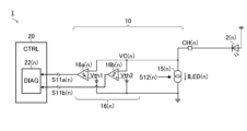
- the switch circuit 10 includes current sources 15(0)-15(7) and detection circuits 16(0)-16(7).
- Current source 15(n) is connected in series to light-emitting element 2(n). In this diagram, current source 15(n) is connected between external terminal CH(n) and the ground terminal. Note that current source 15(n) may be replaced with a switch element.
- the current source 15(n) connected in this manner is on/off controlled according to the drive signal S12(n) output from the PWM dimming circuit 21(n) of the control circuit 20.
- the drive current ILED(n) flows through the light-emitting element 2(n). Therefore, the light-emitting element 2(n) is in a light-on state.
- the drive current ILED(n) no longer flows through the light-emitting element 2(n). Therefore, the light-emitting element 2(n) is in a light-off state.
- the node voltage VC(n) can be understood as the cathode voltage of the light-emitting element 2(n).
- the node voltages VC(0) to VC(7) may be output feedback controlled so that the lowest voltage among them matches a predetermined reference voltage Vfb.
- FIG. 8 is a diagram showing a second embodiment of the semiconductor device 1 (particularly, an example of a detection circuit 16(n) used in the light emitting device 100 of the second configuration example (FIG. 7)).
- the detection circuit 16(n) includes comparators 16a(n) and 16b(n).
- the detection circuit 16(n) outputs detection signals S11a(n) and S11b(n) as the aforementioned detection signal S11(n).
- Comparator 16a(n) outputs detection signal S11a(n) by comparing node voltage VC(n) input to the non-inverting input terminal (+) with threshold voltage Vth1 input to the inverting input terminal (-). Therefore, detection signal S11a(n) is at high level when VC(n)>Vth1, and is at low level when VC(n) ⁇ Vth1.
- threshold voltage Vth1 corresponds to the short circuit detection voltage of light-emitting element 2(n).
- Threshold voltage Vth1 is set to a voltage value higher than reference voltage Vfb.
- Comparator 16b(n) outputs detection signal S11b(n) by comparing node voltage VC(n) input to the inverting input terminal (-) with threshold voltage Vth2 input to the non-inverting input terminal (+). Therefore, detection signal S11b(n) is at low level when VC(n)>Vth2, and at high level when VC(n) ⁇ Vth2.
- threshold voltage Vth2 corresponds to the open detection voltage of light-emitting element 2(n).
- Threshold voltage Vth2 is set to a voltage value lower than reference voltage Vfb.
- the fault diagnosis circuit 22(n) monitors the detection signals S11a(n) and S11b(n) when the drive signal S12(n) of the current source 15(n) is at the on-logic level, and performs short circuit and open circuit diagnosis of the light-emitting element 2(n).
- the fault diagnosis circuit 22(n) monitors at least one of the detection signals S11a(n) and S11b(n) when the drive signal S12(n) of the current source 15(n) is at the off logic level, and performs a stuck-on diagnosis or a stuck-off diagnosis of the current source 15(n).
- Current source 15(n) stuck on (hereinafter sometimes referred to as CS stuck on) refers to a failure mode in which current source 15(n) does not turn off and remains on even though the drive signal S12(n) of current source 15(n) is set to the off logical level.
- Current source 15(n) stuck off (hereinafter sometimes referred to as CS stuck off) refers to a failure mode in which current source 15(n) does not turn on and remains in the off state even though the drive signal S12(n) for current source 15(n) is set to the on logical level.
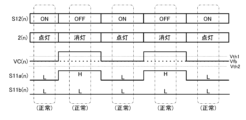
- ⁇ Fault Diagnosis (Second Embodiment)> 9 is a diagram showing a fifth example of fault diagnosis (normal in the second embodiment).
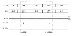
- the drive signal S12(n) of the current source 15(n) the on/off state of the light-emitting element 2(n), the node voltage VC(n), and the detection signals S11a(n) and S11b(n) are depicted.
- the light-emitting element 2(n) and the current source 15(n) are normal, if the drive signal S12(n) of the current source 15(n) is at the off logical level, the current source 15(n) is in the off state. At this time, the drive current ILED does not flow through the light-emitting element 2(n). Therefore, the light-emitting element 2(n) is in the off state.
- the node voltage VC(n) is higher than the threshold voltage Vth1. In other words, Vth2 ⁇ Vth1 ⁇ VC(n) is established. Therefore, the detection signal S11a(n) is at a high level, and the detection signal S11b(n) is at a low level.
- the fault diagnosis circuit 22(n) diagnoses that both the light-emitting element 2(n) and the current source 15(n) are normal when the detection signals S11a(n) and S11b(n) are both at a low level when the drive signal S12(n) is at an on-logic level, and when the detection signal S11a(n) is at a high level and the detection signal S11b(n) is at a low level when the drive signal S12(n) is at an off-logic level.
- FIG. 10 is a diagram showing a sixth example of fault diagnosis (when the LED is short-circuited in the second embodiment). As with FIG. 9, this diagram depicts the drive signal S12(n) of the current source 15(n), the on/off state of the light-emitting element 2(n), the node voltage VC(n), and the detection signals S11a(n) and S11b(n).
- the fault diagnosis circuit 22(n) diagnoses that a short circuit has occurred in the light-emitting element 2(n).
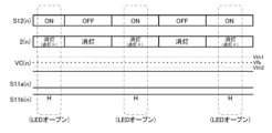
- FIG. 11 is a diagram showing a seventh example of fault diagnosis (when the LED is open in the second embodiment). Note that, like the above-mentioned FIGS. 9 and 10, this diagram depicts the drive signal S12(n) of the current source 15(n), the on/off state of the light-emitting element 2(n), the node voltage VC(n), and the detection signals S11a(n) and S11b(n).
- the node voltage VC(n) is lower than the threshold voltage Vth2. In other words, VC(n) ⁇ Vth2 ⁇ Vth1 is established. Therefore, the detection signal S11a(n) is at a low level, and the detection signal S11b(n) is at a high level.
- the fault diagnosis circuit 22(n) diagnoses that an open circuit has occurred in the light-emitting element 2(n).
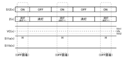
- the fault diagnosis circuit 22(n) diagnoses that the current source 15(n) is stuck on when the detection signal S11a(n) is at a low level at the timing when the drive signal S12(n) is at its off logical level.
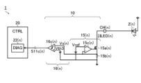
- FIG. 14 is a diagram showing a third embodiment of the semiconductor device 1 (particularly a specific example of the current source 15(n) and a modified example of the detection circuit 16(n) used in the light emitting device 100 of the second configuration example (FIG. 7)).
- the current source 15(n) includes a transistor 15a(n) (an NMOSFET in the example shown in the figure), a resistor 15b(n), and an amplifier 15c(n).
- the detection circuit 16(n) includes a comparator 16c(n).
- the detection circuit 16(n) outputs a detection signal S11c(n) as the aforementioned detection signal S11(n).
- the drain of the transistor 15a(n) is connected to the external terminal CH(n).
- the source of the transistor 15a(n) is connected to the first terminal of the resistor 15b(n).
- the second terminal of the resistor 15b(n) is connected to the ground terminal.
- the reference voltage Vref may be adjustable using a DAC [digital-to-analog converter] or the like.
- Comparator 16c(n) outputs detection signal S11c(n) by comparing sense voltage Vs(n) input to the inverting input terminal (-) with threshold voltage Vth3 input to the non-inverting input terminal (+). Therefore, detection signal S11c(n) is at low level when Vs(n)>Vth3, and at high level when Vs(n) ⁇ Vth3.
- the fault diagnosis circuit 22(n) performs a stuck-on diagnosis or a stuck-off diagnosis of the current source 15(n) by monitoring the detection signal S11c(n) both when the drive signal S12(n) of the current source 15(n) is at the off logic level and when it is at the on logic level.
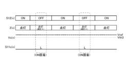
- ⁇ Fault Diagnosis (Third Embodiment)> 15 is a diagram showing a tenth example of fault diagnosis (normal in the third embodiment). In this diagram, from the top, the drive signal S12(n) of the current source 15(n), the on/off state of the light-emitting element 2(n), the sense voltage Vs(n), and the detection signal S11c(n) are depicted.
- the drive signal S12(n) of the current source 15(n) is at the off logical level
- the current source 15(n) is in the off state.
- the drive current ILED does not flow to the light-emitting element 2(n). Therefore, the light-emitting element 2(n) is in the off state.
- the sense voltage Vs(n) becomes lower than the threshold voltage Vth3. Therefore, the detection signal S11c(n) becomes high level.
- the fault diagnosis circuit 22(n) diagnoses that both the light-emitting element 2(n) and the current source 15(n) are normal.
- FIG. 16 is a diagram showing an eleventh example of fault diagnosis (when CS is stuck on in the third embodiment). As with FIG. 15, from the top, this diagram depicts the drive signal S12(n) of the current source 15(n), the on/off state of the light-emitting element 2(n), the sense voltage Vs(n), and the detection signal S11c(n).
- the fault diagnosis circuit 22(n) diagnoses that the current source 15(n) is stuck on when the detection signal S11c(n) is at a low level at the timing when the drive signal S12(n) is at its off logical level.
- FIG. 17 is a diagram showing a twelfth example of fault diagnosis (when CS is stuck off in the third embodiment). As with the above-mentioned FIGS. 15 and 16, this diagram depicts, from top to bottom, the drive signal S12(n) of the current source 15(n), the on/off state of the light-emitting element 2(n), the sense voltage Vs(n), and the detection signal S11c(n).
- the fault diagnosis circuit 22(n) diagnoses that the current source 15(n) is stuck off when the detection signal S11c(n) is at a high level at the timing when the drive signal S12(n) is at the on logical level.
- the second embodiment (FIG. 8) and the third embodiment (FIG. 14) may be combined. By combining the two detection methods, it becomes possible to correctly diagnose the failure mode of each of the light-emitting element 2(n) and the current source 15(n).
- ⁇ Application to vehicles> 18 and 19 are diagrams showing the external appearance (front and rear) of a vehicle on which the above-mentioned light-emitting device 100 can be mounted.
- the light-emitting device 100 can be suitably used, for example, as a headlamp (including high beam/low beam/small lamp/fog lamp, etc., as appropriate) X11, a daytime running lamp (DRL [daylight running lamps]) X12, a tail lamp (including small lamp or back lamp, etc., as appropriate) X13, a stop lamp X14, and a turn lamp X15 of the vehicle X10.
- the light-emitting device 100 may be an interior lamp (such as an instrument panel lamp) of the vehicle X10.
- the semiconductor device disclosed in this specification is configured (first configuration) to include a switch element configured to be connected in parallel to a light-emitting element, a detection circuit configured to generate a detection signal by comparing the voltage across the switch element with a predetermined threshold voltage, and a fault diagnosis circuit configured to diagnose whether the switch element is stuck off by monitoring the detection signal at a timing when the drive signal for the switch element is at an on-logic level.
- the fault diagnosis circuit may be configured (second configuration) to diagnose whether the switch element is stuck on or whether the light-emitting element to which the switch element is connected in parallel is short-circuited by monitoring the detection signal at a timing when the drive signal is at an off logic level.
- the fault diagnosis circuit may be configured to output the fault diagnosis result to the outside of the semiconductor device (third configuration).
- the fault diagnosis circuit may be configured to transition the semiconductor device to a safe state (fourth configuration).
- a semiconductor device may be further configured (fifth configuration) to include a control circuit configured to generate a control signal, and a driver configured to generate the drive signal in response to the control signal.
- the semiconductor device according to the fifth configuration may be further configured (sixth configuration) to include a level shifter configured to shift the signal level of the control signal between the control circuit and the driver.
- the semiconductor device disclosed in this specification is configured (seventh configuration) to include a switch element or a current source configured to be connected in series to a light-emitting element, a detection circuit configured to generate a detection signal by comparing the voltage across the switch element or the current source with a predetermined threshold voltage, and a fault diagnosis circuit configured to diagnose whether the switch element or the current source is stuck on by monitoring the detection signal at a timing when the drive signal for the switch element or the current source is at an off logic level.
- the fault diagnosis circuit may be configured (eighth configuration) to perform a stuck-off diagnosis of the switch element or the current source, or a short circuit diagnosis or open circuit diagnosis of the light-emitting element by monitoring the detection signal at the timing when the drive signal is at the on-logic level.
- the semiconductor device disclosed in this specification is configured (ninth configuration) to include a switch element or a current source configured to be connected in series to a light-emitting element, a detection circuit configured to detect a drive current flowing through the switch element or the current source and generate a detection signal, and a fault diagnosis circuit configured to diagnose whether the switch element or the current source is stuck on by monitoring the detection signal when the drive signal of the switch element or the current source is at a logical level when it is off, and to diagnose whether the switch element or the current source is stuck off by monitoring the detection signal when the drive signal of the switch element or the current source is at a logical level when it is on.
- the light emitting device disclosed in this specification has a configuration (tenth configuration) including the light emitting element and a semiconductor device having any one of the first to ninth configurations described above.
- the light-emitting device may also be configured (eleventh configuration) in which the light-emitting element is an LED element or an organic EL element.
- the vehicle disclosed in this specification is configured to include a light-emitting device according to the tenth or eleventh configuration (twelfth configuration).
Landscapes
- Engineering & Computer Science (AREA)
- Mechanical Engineering (AREA)
- Electronic Switches (AREA)
Priority Applications (1)
| Application Number | Priority Date | Filing Date | Title |
|---|---|---|---|
| JP2024551251A JPWO2024079980A1 (cg-RX-API-DMAC7.html) | 2022-10-14 | 2023-08-17 |
Applications Claiming Priority (2)
| Application Number | Priority Date | Filing Date | Title |
|---|---|---|---|
| JP2022-165470 | 2022-10-14 | ||
| JP2022165470 | 2022-10-14 |
Publications (1)
| Publication Number | Publication Date |
|---|---|
| WO2024079980A1 true WO2024079980A1 (ja) | 2024-04-18 |
Family
ID=90669450
Family Applications (1)
| Application Number | Title | Priority Date | Filing Date |
|---|---|---|---|
| PCT/JP2023/029700 Ceased WO2024079980A1 (ja) | 2022-10-14 | 2023-08-17 | 半導体装置、発光装置、車両 |
Country Status (2)
| Country | Link |
|---|---|
| JP (1) | JPWO2024079980A1 (cg-RX-API-DMAC7.html) |
| WO (1) | WO2024079980A1 (cg-RX-API-DMAC7.html) |
Citations (2)
| Publication number | Priority date | Publication date | Assignee | Title |
|---|---|---|---|---|
| JP2016170931A (ja) * | 2015-03-12 | 2016-09-23 | 三菱自動車工業株式会社 | コンタクタの故障判定装置 |
| JP2020031066A (ja) * | 2019-11-22 | 2020-02-27 | ローム株式会社 | スイッチ駆動装置、発光装置、車両 |
-
2023
- 2023-08-17 WO PCT/JP2023/029700 patent/WO2024079980A1/ja not_active Ceased
- 2023-08-17 JP JP2024551251A patent/JPWO2024079980A1/ja active Pending
Patent Citations (2)
| Publication number | Priority date | Publication date | Assignee | Title |
|---|---|---|---|---|
| JP2016170931A (ja) * | 2015-03-12 | 2016-09-23 | 三菱自動車工業株式会社 | コンタクタの故障判定装置 |
| JP2020031066A (ja) * | 2019-11-22 | 2020-02-27 | ローム株式会社 | スイッチ駆動装置、発光装置、車両 |
Also Published As
| Publication number | Publication date |
|---|---|
| JPWO2024079980A1 (cg-RX-API-DMAC7.html) | 2024-04-18 |
Similar Documents
| Publication | Publication Date | Title |
|---|---|---|
| US10360969B2 (en) | Light emitting element driving semiconductor integrated circuit, light emitting element driving device, light emitting device, and vehicle | |
| KR20170045218A (ko) | Led 주행등 제어 및 상태를 위한 장치 및 방법 | |
| EP3220719B1 (en) | Light emitting element driving device, light emitting device, and vehicle | |
| EP3244700B1 (en) | Ground fault detection circuit, abnormality detection circuit, light emitting device, vehicle | |
| JP6783790B2 (ja) | 点灯回路、車両用灯具 | |
| WO2021206145A1 (ja) | 車両用灯具および点灯回路 | |
| JP7503177B2 (ja) | ランプ制御装置 | |
| WO2024079980A1 (ja) | 半導体装置、発光装置、車両 | |
| CN114928915A (zh) | 点亮电路 | |
| JP2019169655A (ja) | 発光素子駆動装置 | |
| WO2021251374A1 (ja) | 光源モジュールおよび点灯回路 | |
| JP2007305929A (ja) | Led表示装置及びled照明装置 | |
| JP7643992B2 (ja) | 点灯回路、及び車両用灯具 | |
| CN219421111U (zh) | 一种应用于三极管线性恒流电路的短路n-1保护电路 | |
| JP7374179B2 (ja) | 発光素子駆動装置 | |
| CN118541287A (zh) | 点亮电路 | |
| KR20120003730A (ko) | 차량용 리어 콤비네이션 램프 제어회로 | |
| CN113940142A (zh) | 灯具模块及其点亮电路 | |
| JP7675637B2 (ja) | 点灯回路、及び車両用灯具 | |
| WO2024096118A1 (ja) | リアターンランプ | |
| KR20190067615A (ko) | 차량용 헤드램프 제어 장치 | |
| JP2022118962A (ja) | 点灯回路 | |
| JP2025080399A (ja) | 点灯モジュール | |
| JP2025051209A (ja) | 灯具、点灯回路及び半導体装置 | |
| WO2024127916A1 (ja) | 車両用灯具制御装置 |
Legal Events
| Date | Code | Title | Description |
|---|---|---|---|
| 121 | Ep: the epo has been informed by wipo that ep was designated in this application |
Ref document number: 23876988 Country of ref document: EP Kind code of ref document: A1 |
|
| WWE | Wipo information: entry into national phase |
Ref document number: 2024551251 Country of ref document: JP |
|
| NENP | Non-entry into the national phase |
Ref country code: DE |
|
| 122 | Ep: pct application non-entry in european phase |
Ref document number: 23876988 Country of ref document: EP Kind code of ref document: A1 |