WO2024075591A1 - 発光素子駆動装置、および発光システム - Google Patents
発光素子駆動装置、および発光システム Download PDFInfo
- Publication number
- WO2024075591A1 WO2024075591A1 PCT/JP2023/034912 JP2023034912W WO2024075591A1 WO 2024075591 A1 WO2024075591 A1 WO 2024075591A1 JP 2023034912 W JP2023034912 W JP 2023034912W WO 2024075591 A1 WO2024075591 A1 WO 2024075591A1
- Authority
- WO
- WIPO (PCT)
- Prior art keywords
- light
- emitting element
- current
- terminal
- driving device
- Prior art date
- Legal status (The legal status is an assumption and is not a legal conclusion. Google has not performed a legal analysis and makes no representation as to the accuracy of the status listed.)
- Ceased
Links
Images


Classifications
-
- H—ELECTRICITY
- H05—ELECTRIC TECHNIQUES NOT OTHERWISE PROVIDED FOR
- H05B—ELECTRIC HEATING; ELECTRIC LIGHT SOURCES NOT OTHERWISE PROVIDED FOR; CIRCUIT ARRANGEMENTS FOR ELECTRIC LIGHT SOURCES, IN GENERAL
- H05B45/00—Circuit arrangements for operating light-emitting diodes [LED]
- H05B45/30—Driver circuits
- H05B45/345—Current stabilisation; Maintaining constant current
-
- H—ELECTRICITY
- H05—ELECTRIC TECHNIQUES NOT OTHERWISE PROVIDED FOR
- H05B—ELECTRIC HEATING; ELECTRIC LIGHT SOURCES NOT OTHERWISE PROVIDED FOR; CIRCUIT ARRANGEMENTS FOR ELECTRIC LIGHT SOURCES, IN GENERAL
- H05B45/00—Circuit arrangements for operating light-emitting diodes [LED]
- H05B45/30—Driver circuits
- H05B45/37—Converter circuits
- H05B45/3725—Switched mode power supply [SMPS]
- H05B45/38—Switched mode power supply [SMPS] using boost topology
-
- H—ELECTRICITY
- H05—ELECTRIC TECHNIQUES NOT OTHERWISE PROVIDED FOR
- H05B—ELECTRIC HEATING; ELECTRIC LIGHT SOURCES NOT OTHERWISE PROVIDED FOR; CIRCUIT ARRANGEMENTS FOR ELECTRIC LIGHT SOURCES, IN GENERAL
- H05B45/00—Circuit arrangements for operating light-emitting diodes [LED]
- H05B45/50—Circuit arrangements for operating light-emitting diodes [LED] responsive to malfunctions or undesirable behaviour of LEDs; responsive to LED life; Protective circuits
-
- H—ELECTRICITY
- H05—ELECTRIC TECHNIQUES NOT OTHERWISE PROVIDED FOR
- H05B—ELECTRIC HEATING; ELECTRIC LIGHT SOURCES NOT OTHERWISE PROVIDED FOR; CIRCUIT ARRANGEMENTS FOR ELECTRIC LIGHT SOURCES, IN GENERAL
- H05B47/00—Circuit arrangements for operating light sources in general, i.e. where the type of light source is not relevant
- H05B47/10—Controlling the light source
- H05B47/105—Controlling the light source in response to determined parameters
- H05B47/14—Controlling the light source in response to determined parameters by determining electrical parameters of the light source
-
- H—ELECTRICITY
- H05—ELECTRIC TECHNIQUES NOT OTHERWISE PROVIDED FOR
- H05B—ELECTRIC HEATING; ELECTRIC LIGHT SOURCES NOT OTHERWISE PROVIDED FOR; CIRCUIT ARRANGEMENTS FOR ELECTRIC LIGHT SOURCES, IN GENERAL
- H05B47/00—Circuit arrangements for operating light sources in general, i.e. where the type of light source is not relevant
- H05B47/20—Responsive to malfunctions or to light source life; for protection
- H05B47/25—Circuit arrangements for protecting against overcurrent
Definitions
- This disclosure relates to a light-emitting element driving device.
- LEDs which consume little power and have a long lifespan, have been used for a variety of purposes.
- LEDs are an example of a light-emitting element.
- a conventional example of an LED driver that drives an LED is disclosed in Patent Document 1.
- the voltage at the LED terminal may not drop low enough to detect an abnormality, meaning that the abnormality cannot be detected and the LED may continue to emit abnormal light.
- the present disclosure aims to provide a light-emitting element driving device that can effectively detect abnormal light emission from a light-emitting element.
- the exemplary light-emitting element driving device of the present disclosure includes an overcurrent detection unit that is configured to be connectable to at least one current detection resistor provided between an application terminal of a power supply voltage for driving at least one channel of a light-emitting element unit and the positive electrode of the light-emitting element unit, and that is configured to detect an overcurrent in the current flowing through the light-emitting element unit.
- the exemplary light-emitting element driving device disclosed herein can effectively detect abnormal light emission from a light-emitting element.
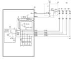
- FIG. 1 is a diagram showing a configuration of a light-emitting system according to a comparative example.
- FIG. 2 is a diagram showing a configuration of a light-emitting system according to the first embodiment of the present disclosure.
- FIG. 3 is a diagram showing a configuration of a light-emitting system according to the second embodiment of the present disclosure.
- FIG. 4 is a diagram showing a configuration of a light-emitting system according to a third embodiment of the present disclosure.
- FIG. 5 is a diagram showing a configuration of a light-emitting system according to a fourth embodiment of the present disclosure.
- FIG. 6 is a diagram showing a configuration of a light-emitting system according to a fifth embodiment of the present disclosure.
- FIG. 1 is a diagram showing a configuration of a light-emitting system according to a comparative example.
- FIG. 2 is a diagram showing a configuration of a light-emitting system according to the first embodiment of the present disclosure.
- FIG. 7 is a diagram showing a configuration of a light-emitting system according to a sixth embodiment of the present disclosure.
- FIG. 8 is a diagram showing a configuration of a light-emitting system according to an eighth embodiment of the present disclosure.
- FIG. 9 is a diagram showing an example of the configuration of a backlight device.
- FIG. 10 is a diagram showing an example of an in-vehicle display.
- Comparative Example Here, a comparative example will be described first for comparison with the embodiment of the present disclosure. By describing the comparative example, the problem will become more clear.
- FIG. 1 is a diagram showing the configuration of a light-emitting system 50 according to a comparative example.
- the light-emitting system 50 shown in FIG. 1 includes an LED driving device (light-emitting element driving device) 20, an output stage 30, and LED arrays 41 to 44.
- the LED driver 20 drives multiple channels (four channels in this embodiment) of LED arrays (light-emitting element units) 41 to 44.
- the LED driver 20 is a semiconductor device that integrates a minimum voltage selection unit 1, a DC/DC control unit 2, a constant current driver 3, an output discharge unit 4, and an output short circuit protection circuit 5 (SCP (short circuit protection)).
- SCP short circuit protection
- the LED driver 20 also has an OUTL terminal, a VDISC terminal, and LED1 to LED4 terminals as external terminals for establishing electrical connection with the outside. Note that for convenience, only a portion of the configuration of the LED driver 20 shown in FIG. 1 is shown, and in reality, the device has other external terminals such as a VCC terminal, and is also provided with an internal voltage generator (VREG) and various protection circuits such as UVLO (Under Voltage Lock Out).
- VREG internal voltage generator
- UVLO Under Voltage Lock Out
- an output stage 30 is arranged to generate an output voltage Vout from an input voltage Vin by DC/DC conversion and supply it to the anodes (positive poles) of the LED arrays 41 to 44.
- the output stage 30 has a switching element N1, a diode D1, an inductor L1, and an output capacitor Co.
- the output stage 30 is controlled by the LED driver 20 as the switching element N1 is driven and controlled by the LED driver 20.
- the output stage 30 and the LED driver 20 form a DC/DC converter.
- a step-up DC/DC converter is particularly configured as the DC/DC converter.
- the application terminal of the input voltage Vin is connected to one terminal of the inductor L1.
- the other terminal of the inductor L1 is connected to the anode of the diode D1 and the drain of a switching element N1 composed of an n-channel metal-oxide-semiconductor field-effect transistor (MOSFET).
- MOSFET metal-oxide-semiconductor field-effect transistor
- the source of the switching element N1 is connected to the ground terminal.
- the gate of the switching element N1 is connected to the OUTL terminal.
- the cathode of the diode D1 is connected to one terminal of the output capacitor Co.
- the other terminal of the output capacitor Co is connected to the ground terminal.
- An output voltage Vout is generated at one terminal of the output capacitor Co.
- the switching element N1 may be included in the LED driving device 20.
- the anodes of the LED arrays 41 to 44 are connected to one end of the output capacitor Co, which generates the output voltage Vout.
- the LED arrays 41 to 44 are each composed of multiple LEDs connected in series.
- the cathodes of the LED arrays 41 to 44 are connected to the LED1 terminal to the LED4 terminal, respectively.
- the LED arrays 41 to 44 are not limited to being connected in series, and may be composed of LEDs connected in series and parallel, or may be composed of only one LED.
- the number of drivable LED arrays (number of channels) is also not limited to four, and may be, for example, six.
- LED terminal voltages Vled1 to Vled4 are applied to the LED1 to LED4 terminals as the cathode voltages of the LED arrays 41 to 44, respectively.
- Minimum voltage selection unit 1 selects the lowest voltage among the LED terminal voltages Vled1 to Vled4.
- the DC/DC control unit 2 has an error amplifier 21.
- the output terminal of the minimum voltage selection unit 1 is connected to the non-inverting input terminal (+) of the error amplifier 21.
- the application terminal of the reference voltage Vref is connected to the inverting input terminal (-) of the error amplifier 21.
- the DC/DC control unit 2 has, for example, a slope generation unit, a PWM comparator, a driver, etc. (not shown) other than the error amplifier 21, and generates a gate signal GS by PWM control based on the error signal between the output of the minimum voltage selection unit 1 and the reference voltage Vref output from the error amplifier 21.
- the generated gate signal GS is applied to the gate of the switching element N1 via the OUTL terminal, thereby controlling the on/off of the switching element N1.
- the output voltage Vout is controlled so that the minimum voltage among the LED terminal voltages Vled1 to Vled4 matches the reference voltage Vref.
- the constant current driver 3 has four channels of constant current circuits 31 arranged between each of the LED1 to LED4 terminals and the ground terminal.
- the constant current value of the current flowing through the constant current circuit 31 can be set by an LED current setting unit (not shown).
- the VDISC terminal is connected to the output discharge unit 4.
- the VDISC terminal is connected to one end of the output capacitor Co where the output voltage Vout is generated. If the output capacitor Co still has charge when started up, the LED may flicker. For this reason, it is desirable for no charge to remain in the output capacitor Co at startup. Therefore, the output discharge unit 4 discharges the residual charge in the output capacitor Co. This discharge is performed when the DC/DC converter is off (when the signal applied to the enable terminal, not shown, falls, or during protection).
- the output short circuit protection circuit (SCP) 5 which is provided as one of the protection functions, has ground fault detection comparators 5A to 5D provided corresponding to each channel of the LED arrays 41 to 44.
- the ground fault detection comparators 5A to 5D have a non-inverting input terminal to which each of the LED terminal voltages Vled1 to Vled4 is applied, and an inverting input terminal to which a reference voltage Vref_sht for ground fault detection is applied.
- the output short circuit protection circuit 5 starts counter operation, and after about 13 ms, for example, the output is latched and all circuits other than the internal voltage generation unit (not shown) are shut down.
- the LED terminal voltage Vled4 will be the lowest compared to the other LED terminal voltages, and the DC/DC converter will perform a boost operation. However, because the LED terminal voltage Vled4 does not rise, the output short-circuit protection circuit 5 stops the operation of the DC/DC converter, and no current flows through the LED arrays 41 to 44. As a result, the LED arrays 41 to 44 are turned off.
- the LED terminal voltage of the channel where the ground fault occurred may not be low enough to be detected by the ground fault detection comparators 5A to 5D.
- ground fault protection is not activated, the DC/DC converter continues to operate, and a larger current than normal flows through the LED array of the channel where the ground fault occurred due to the current path from the cathode to the ground end formed by the ground fault.
- the display device may shine brighter than the set brightness, which may cause problems such as blocking the driver's view.
- excessive current flowing through the LED increases the load on the components in the DC/DC converter, requiring the components to have excess resistance.
- the inventors of the present application have conducted extensive research into a technology that can more reliably detect abnormal light emission from the LED arrays 41-44 (light-emitting element portions), as described below.
- a light-emitting system 501 The configuration of a light-emitting system 501 according to the first embodiment of the present disclosure is shown in Fig. 2.
- the configuration shown in Fig. 2 differs from the comparative example (Fig. 1) in that a current detection resistor R1 is provided outside the LED driving device 201, and further in the configuration of the LED driving device 201 and an MCU (microcomputer) 25. That is, the light-emitting system 501 has a current detection resistor R1 and an MCU 25.
- the first end of the current detection resistor R1 is connected to the application terminal of the output voltage Vout.
- the second end of the current detection resistor R1 is connected to the anodes of the LED arrays 41 to 44. In other words, the current detection resistor R1 is provided after the output stage 30.
- the LED driver 201 has an overcurrent detection unit 6 and an OCD terminal (overcurrent detection terminal) as an external terminal for connecting the current detection resistor R1.
- the overcurrent detection unit 6 has an amplifier 61 and a comparator 62.
- the inverting input terminal of the amplifier 61 is connected to the first terminal of the current detection resistor R1 via the VDISC terminal.
- the non-inverting input terminal of the amplifier 61 is connected to the second terminal of the current detection resistor R1 via the OCD terminal.
- the inverting input terminal of the comparator 62 is connected to the output terminal of the amplifier 61.
- the non-inverting input terminal of the comparator 62 is connected to the application terminal of the reference voltage Va for overcurrent detection.
- the total current Ia which is the sum of the currents flowing through each channel of the LED arrays 41 to 44, is converted to a current/voltage by the current detection resistor R1.
- the converted voltage appears across the current detection resistor R1 and is amplified by an amplifier 61 at a predetermined gain.
- the amplified voltage is compared with a reference voltage Va by the comparator 62, and the comparison result is output as a flag signal Flg.
- the comparator 62 can detect the overcurrent.
- the overcurrent detection unit 6 can detect an overcurrent in the current flowing through the LED arrays 41 to 44 (light-emitting element unit).
- the LED driver 201 has an FG terminal (flag terminal) and an EN terminal (enable terminal) as external terminals.
- the MCU 25 is externally connected to the FG terminal and the EN terminal.
- the flag signal Flg output from the comparator 62 is input to the MCU 25 via the FG terminal.
- the MCU 25 can output the enable signal Eb via the EN terminal to an internal voltage generator 7 provided in the LED driver 201.
- the internal voltage generator 7 generates an internal power supply voltage Vreg based on a power supply voltage applied to a VCC terminal (not shown) provided in the LED driver 201.
- the internal power supply voltage Vreg is generated when the enable signal Eb is in an enabled state, and is used as a power supply voltage for the internal circuit of the LED driver 201.
- the MCU 25 disables the enable signal Eb. This stops the operation of the internal voltage generation unit 7, and the internal power supply voltage Vreg drops.
- the UVLO unit 8 provided in the LED drive device 201 detects the drop in the internal power supply voltage Vreg and commands the DC/DC control unit 2 to stop the operation of the DC/DC converter. This stops the switching of the switching element N1, stops current flowing to the LED arrays 41 to 44, and releases the abnormal light emission state.
- Second Embodiment 3 is a diagram showing the configuration of a light-emitting system 502 according to a second embodiment of the present disclosure.
- the difference in configuration from the first embodiment (FIG. 2) of the configuration shown in FIG. 3 is the configurations of the LED driver 202 and the MCU 25.
- the LED driver 202 has an LED current setting unit 9 and a communication unit 10. Note that the LED current setting unit 9 is also provided in the first embodiment.
- the communication unit 10 is configured to communicate with the MCU 25, for example, by SPI (Serial Peripheral Interface).
- the communication unit 10 has a register 10A. Various types of information are stored in the register 10A.
- the LED driver 202 has an ADIM terminal (dimming terminal) as an external terminal.
- the MCU 25 can dim the LED arrays 41 to 44 by outputting a dimming signal Dm to the LED current setting unit 9 via the ADIM terminal. This type of dimming is called DC dimming.
- the LED current setting unit 9 has an error amplifier 91 and an output transistor 92.
- the non-inverting input terminal of the error amplifier 91 is connected to the application terminal of the reference voltage Vref_led for setting the LED current.
- the output terminal of the error amplifier 91 is connected to the gate of the output transistor 92 composed of an n-channel MOSFET.
- the source of the output transistor 92 is connected to the inverting input terminal of the error amplifier 91.
- the LED driver 202 has an ISET terminal (current setting terminal) as an external terminal.
- the first terminal of the setting resistor Reset is externally connected to the ISET terminal.
- the ISET terminal is connected to the source of the output transistor 92.
- the voltage at the ISET terminal is controlled to match the reference voltage Vref_led, and a current flows through the ISET terminal at a current value determined by the voltage at the ISET terminal and the setting resistor Reset.
- a current proportional to the current flowing through the ISET terminal flows through each constant current circuit 31.
- the reference voltage Vref_led is variable according to the dimming signal Dm, and the LED current can be set by the dimming signal Dm.
- the operation of the DC/DC converter may be stopped by disabling the enable signal Eb, as in the first embodiment.
- the communication unit 10 may not be provided, and when the MCU 25 receives a flag signal Flg indicating an abnormality from the FG terminal, as in the first embodiment, the dimming signal Dm may be used to dim the LEDs to reduce their brightness.
- Third Embodiment 4 is a diagram showing the configuration of a light-emitting system 503 according to a third embodiment of the present disclosure.
- the difference in configuration from the second embodiment (FIG. 3) of the configuration shown in FIG. 4 is the configuration of the LED driving device 203.
- the LED driver 203 has a flag output unit 11.
- the flag output unit 11 In addition to the output Cp1 of the comparator 62 in the overcurrent detection unit 6, the flag output unit 11 also receives outputs from various protection circuits 12 (SCP, TSD (thermal shutdown), UVLO, etc.) not shown.
- the flag output unit 11 outputs a flag signal Flg from the FLG terminal to the MCU 25 based on Cp1 and the outputs from the various protection circuits 12. Specifically, if any one of the outputs including Cp1 indicates an abnormality, the flag signal Flg reaches a level indicating an abnormality.
- the MCU 25 When the MCU 25 receives a flag signal Flg with a level indicating an abnormality, it communicates with the communication unit 10 to read the register 10A in order to determine the specific type of abnormality.
- the register 10A stores information indicating which abnormality has been detected by the overcurrent detection unit 6 and the various protection circuits 12.
- the MCU 25 When the MCU 25 reads the register 10A and determines that an overcurrent abnormality has been detected by the overcurrent detection unit 6, the MCU 25 performs dimming to reduce the brightness of the LED using the dimming signal Dm, as in the second embodiment.
- the MCU 25 may stop the operation of the DC/DC converter using the enable signal Eb, for example, when an overcurrent abnormality has been detected by the overcurrent detection unit 6 and a ground fault has been detected at the cathode of the LED by the output short circuit protection circuit (SCP).
- SCP output short circuit protection circuit
- FIG. 5 is a diagram showing the configuration of a light-emitting system 504 according to a fourth embodiment of the present disclosure.
- the difference in configuration from the first embodiment (Fig. 2) of the configuration shown in Fig. 5 is that current detection resistors Ra to Rd are provided. That is, the light-emitting system 504 has current detection resistors Ra to Rd.
- Current detection resistors Ra to Rd are provided corresponding to each channel of the LED arrays 41 to 44. Specifically, the first terminals of the current detection resistors Ra to Rd are commonly connected to the application terminal of the output voltage Vout. The second terminals of the current detection resistors Ra to Rd are connected to the anodes of the LED arrays 41 to 44, respectively.
- the LED driver 204 has overcurrent detection units 6A to 6D and terminals OCD1 to OCD4.
- the overcurrent detection units 6A to 6D are provided corresponding to each channel of the LED arrays 41 to 44.
- Each of the overcurrent detection units 6A to 6D has an amplifier 61 and a comparator 62. More specifically, a first end of the current detection resistor Ra is connected to the inverting input end of the amplifier 61 of the overcurrent detection unit 6A, and a second end of the current detection resistor Ra is connected to the non-inverting input end of the amplifier 61 of the overcurrent detection unit 6A via the OCD1 terminal. Similarly, both ends of resistors Rb, Rc, and Rd are connected to the input ends of the amplifier 61 of the overcurrent detection units 6B to 6D.
- the LED driver 204 has terminals FG1 to FG4 corresponding to the overcurrent detectors 6A to 6D.
- the flag signals Flg1 to Flg4 output from the comparators 62 of the overcurrent detectors 6A to 6D are sent to the MCU 25 via the terminals FG1 to FG4, respectively.
- the overcurrent detection units 6A to 6D can detect overcurrent for each channel of the LED arrays 41 to 44. Therefore, the MCU 25 can determine in which channel an overcurrent abnormality is occurring, based on the flag signals Flg1 to Flg4.
- the LED driver 204 has LED current setting units 9A to 9D.
- the LED current setting units 9A to 9D are provided corresponding to each channel of the LED arrays 41 to 44.
- Each of the LED current setting units 9A to 9D has an error amplifier 91 and an output transistor 92.
- the setting resistor Reset may be shared by the LED current setting units 9A to 9D, or may be provided for each of the LED current setting units 9A to 9D.
- the LED driver 204 has ADIM1 terminals to ADIM4 terminals corresponding to the LED current setting units 9A to 9D.
- the MCU 25 outputs dimming signals Dm1 to Dm4 to the LED current setting units 9A to 9D via the ADIM1 to ADIM4 terminals, respectively.
- the dimming signal Dm1 varies the reference voltage Vref_led1 in the LED current setting unit 9A, and the dimming signal Dm1 enables dimming of the LED array 41 (first channel).
- the dimming signals Dm2 to Dm4 vary the reference voltages Vref_led2 to Vref_led4 in the LED current setting units 9B to 9D, respectively, and the dimming signals Dm2 to Dm4 enable dimming of the LED arrays 42 to 44 (second to fourth channels).
- the MCU 25 determines which channel an overcurrent abnormality is occurring in based on the flag signals Flg1 to Flg4, and performs dimming to reduce the LED brightness using the dimming signals Dm1 to Dm4 corresponding to the determined channel. For example, if an overcurrent abnormality is occurring in the LED array 44 of the fourth channel, the overcurrent abnormality is detected by the flag signal Flg4, and the reference voltage Vref_led4 in the LED current setting unit 9D is changed by the dimming signal Dm4 so that it is lower than normal. This suppresses abnormal light emission in the fourth channel.
- overcurrent abnormalities can be detected for each channel and only the abnormal channel can be dimmed, so protection can be achieved without reducing the brightness of the entire LED array 41 to 44 as much as possible.
- the FG1 to FG4 terminals may not be provided, but a communication unit 10 may be provided, the output states of the overcurrent detection units 6A to 6D may be stored in a register 10A of the communication unit 10, and the MCU 25 may read the register 10A via communication. This also allows the MCU 25 to determine in which channel an overcurrent abnormality is occurring.
- Fifth Embodiment 6 is a diagram showing a configuration of a light-emitting system 505 according to a fifth embodiment of the present disclosure.
- a current detection resistor Ra is provided corresponding to the pair of LED arrays 41 and 42 (first and second channels), and a resistor Rb is provided corresponding to the pair of LED arrays 43 and 44 (third and fourth channels). More specifically, the first terminals of the current detection resistors Ra and Rb are commonly connected to the application terminal of the output voltage Vout, the second terminals of the current detection resistor Ra are connected to the anodes of the LED arrays 41 and 42, and the second terminals of the resistor Rb are connected to the anodes of the LED arrays 43 and 44.
- LED driving device 205 of this embodiment overcurrent detection units 6A, 6B and OCD1, OCD2 terminals are provided corresponding to the current detection resistors Ra, Rb.
- FG1, FG2 terminals are provided as flag terminals
- ADIM1, ADIM2 terminals are provided as dimming terminals
- LED current setting units 9A, 9B are provided.
- LED current setting units 9A, 9B correspond to the set of LED arrays 41, 42 and the set of LED arrays 43, 44, respectively.
- This configuration makes it possible to detect overcurrent abnormalities and adjust the brightness for each pair of LED arrays 41 and 42 and for each pair of LED arrays 43 and 44. This makes it possible to reduce the number of external terminals in the LED driving device while achieving the same effect as the fourth embodiment.
- Sixth Embodiment 7 is a diagram showing a configuration of a light-emitting system 506 according to a sixth embodiment of the present disclosure.
- an MCU as in the first to fifth embodiments is not used.
- the LED driving device 206 of this embodiment has a dimming control unit 13.
- the dimming control unit 13 variably controls the reference voltage Vref_led in the LED current setting unit 9.
- the dimming control unit 13 changes Vref_led in the LED current setting unit 9 to be lower than normal. This reduces the currents flowing through the LED arrays 41 to 44, providing protection. According to this embodiment, protection can be achieved by feedback to the LED current setting unit 9 within the LED driver 206, without using an MCU.
- the dimming control unit 13 may control the LED current setting unit 9 corresponding to the channel in which an overcurrent abnormality is detected. This makes it possible to obtain the same effect as the fourth or fifth embodiment without using an MCU.
- the reference voltage Va for detecting an overcurrent may be variable.
- the reference voltage Va may be variable based on a setting resistor Reset externally connected to an ISET terminal (current setting terminal).
- the overcurrent threshold value can be set according to the LED current setting.
- FIG. 8 is a diagram showing a configuration of a light-emitting system 507 according to an eighth embodiment of the present disclosure.
- a p-channel MOSFET 35 is provided in addition to a current detection resistor R1.
- a first end of the current detection resistor R1 is connected to the application end of the output voltage Vout.
- a second end of the current detection resistor R1 is connected to the source of the p-channel MOSFET 35 at node N1.
- the drain of the p-channel MOSFET 35 is connected to each anode of the LED arrays 41 to 44.
- the LED driving device 207 of this embodiment has an overcurrent detection unit 14.
- the LED driving device 207 also has a PGT terminal (gate connection terminal) as an external terminal.
- the overcurrent detection unit 14 has a current limiting unit 141 and a comparator 142.
- the current limiting unit 141 has an amplifier 141A.
- the inverting input terminal of the amplifier 141A is connected to the node N1 via the OCD terminal.
- a voltage that is lower than the output voltage Vout by the reference voltage Vb1 is applied to the non-inverting input terminal of the amplifier 141A.
- the output terminal of the amplifier 141A is connected to the gate (control terminal) of the p-channel MOSFET 35 via the PGT terminal.
- the amplifier 141A controls the gate voltage of the p-channel MOSFET 35 to be higher. This increases the impedance between the drain and source of the p-channel MOSFET 35. This reduces the total current Ia, and the current flowing through the LED arrays 41 to 44 is suppressed.
- the reference voltage Vb1 in the current limiting unit 141 is set to a voltage value corresponding to a current setting value greater than the maximum value of the total current Ia due to current value variation in the constant current driver 3.
- the non-inverting input terminal of the comparator 142 is connected to the PGT terminal.
- the inverting input terminal of the comparator 142 is connected to the application terminal of the reference voltage Vb2. This causes the comparator 142 to output the comparison result between the gate voltage of the p-channel MOSFET 35 and the reference voltage Vb2.
- a backlight device will be described as an example of an application of the LED driving device according to the embodiment described above.
- a configuration example of a backlight device to which the LED driving device can be applied is shown in Fig. 9. Note that the configuration shown in Fig. 9 is a so-called edge light type, but is not limited to this and may be a direct type configuration.
- the backlight device 70 shown in FIG. 9 is an illumination device that illuminates the liquid crystal panel 81 from the back.
- the backlight device 70 includes an LED light source device 71, a light guide plate 72, a reflector plate 73, and optical sheets 74.
- the LED light source device 71 includes an LED and a substrate on which the LED is mounted. Light emitted from the LED light source device 71 enters the interior from the side of the light guide plate 72.
- the light guide plate 72 which is made of an acrylic plate, for example, totally reflects the light that enters the interior and guides it throughout the interior, and emits it as planar light from the side on which the optical sheets 74 are arranged.
- the reflector plate 73 reflects the light leaking from the light guide plate 72 back into the light guide plate 72.
- the optical sheets 74 are made of a diffusion sheet, a lens sheet, etc., and are intended to uniformize and improve the brightness of the light illuminating the liquid crystal panel 81.
- the light emitting system of the various embodiments described above can be used as the LED light source device 71.
- a backlight device to which the LED driving device according to the embodiment described above is applied is particularly suitable for mounting on an in-vehicle display.
- the in-vehicle display is mounted on the dashboard in front of the driver's seat of the vehicle, for example, as in the in-vehicle display 85 shown in FIG. 10.
- the in-vehicle display 85 can display various images, such as car navigation information, captured images of the rear of the vehicle, a speedometer, a fuel gauge, a fuel consumption meter, and a shift position, and can convey various information to the user.
- Such an in-vehicle display is also called a cluster panel or a center information display (CID).
- the in-vehicle display may be a rear entertainment device disposed, for example, behind the driver's seat or passenger seat.
- the light-emitting element driving device (201) is configured to be connectable to at least one current detection resistor (R1) provided between the application terminal of a power supply voltage (Vout) for driving at least one channel of a light-emitting element unit (41 to 44) and the positive electrode of the light-emitting element unit, and is configured to detect an overcurrent of a current flowing in the light-emitting element unit (first configuration).
- R1 current detection resistor
- the overcurrent detection unit (6) may be configured to have an amplifier (61) having an input terminal configured to be connected to the current detection resistor (R1), and a first comparator (62) configured to compare the output of the amplifier with a first reference voltage (Va) (second configuration).
- a constant current driver (3) configured to be connectable to a negative electrode of the light-emitting element unit; a current setting terminal (ISET terminal) which is an external terminal connectable to a setting resistor (Reset); a current setting unit (9) configured to set a current value of the constant current driver based on the setting resistor; Equipped with The first reference voltage (Va) may be variably set based on the setting resistor (third configuration).
- an external terminal may be provided for outputting the detection result of the overcurrent detection unit (6) to the outside (fourth configuration).
- the external terminal may be configured to be connectable to an external MCU (25) (fifth configuration).
- the sixth configuration may include a flag output unit (11) configured to generate a flag signal (Flg) based on the detection result by the protection circuit in addition to the detection result and output the flag signal via the external terminal.
- a configuration may be provided that includes a register (10A) capable of storing the detection result of the overcurrent detection unit as information, and a communication unit (10) configured to be capable of communicating with an external MCU (25) (seventh configuration).
- a constant current driver (3) configured to be connectable to a negative electrode of the light-emitting element unit;
- a current setting unit (9) configured to set a current value of the constant current driver;
- the eighth configuration may further include a dimming control unit (13) configured to cause the current setting unit to set the current value lower than normal when an overcurrent abnormality is detected by the overcurrent detection unit (6).
- the current detection resistors (Ra to Rd) may be provided for each of the multiple channels, and the overcurrent detection units (6A to 6D) may be provided for each of the multiple current detection resistors (ninth configuration, FIG. 5).
- the current detection resistors (Ra, Rb) may be provided for each of a plurality of groups consisting of a plurality of the channels, and the overcurrent detection units (6A, 6B) may be provided for each of the plurality of current detection resistors (tenth configuration, FIG. 6).
- a light-emitting system (501) includes a light-emitting element driving device (201) having any one of the first to tenth configurations described above, the current detection resistor (R1), an MCU (25), and a DC/DC converter configured to generate the power supply voltage (Vout), and when an overcurrent abnormality is detected by the overcurrent detection unit (6), the MCU is configured to instruct the light-emitting element driving device to stop the operation of the DC/DC converter (eleventh configuration).
- a light-emitting system (502) includes a light-emitting element driving device (202) having any one of the first to tenth configurations, the current detection resistor (R1), and an MCU (25),
- the light-emitting element driving device (202) includes a constant current driver (3) configured to be connectable to a negative electrode of the light-emitting element unit, and a current setting unit (9) configured to set a current value of the constant current driver,
- the MCU is configured to send a dimming signal (Dm) to the light-emitting element driving device so as to cause the current setting unit to set the current value lower than normal (12th configuration).
- a light-emitting system (507) includes a light-emitting element driving device (207) having any one of the first to tenth configurations described above, the current detection resistor (R1), and a transistor (35) connected between the current detection resistor and the positive electrode of the light-emitting element portion, and the overcurrent detection unit (14) has a current limiting unit (141) configured to limit the current flowing through the current detection resistor by controlling the control terminal of the transistor, and is configured to detect the overcurrent based on the voltage of the control terminal (13th configuration).
- the current limiting unit (141) may be configured to have an amplifier (141A) including a first input terminal configured to be connectable to a node (N1) to which the current detection resistor (R1) and the transistor (35) are connected, a second input terminal configured to be connected to an application terminal of a voltage lower than a predetermined voltage (Vout) by a second reference voltage (Vb1), and an output terminal configured to be connectable to the control terminal (14th configuration).
- an amplifier (141A) including a first input terminal configured to be connectable to a node (N1) to which the current detection resistor (R1) and the transistor (35) are connected, a second input terminal configured to be connected to an application terminal of a voltage lower than a predetermined voltage (Vout) by a second reference voltage (Vb1), and an output terminal configured to be connectable to the control terminal (14th configuration).
- the overcurrent detection unit (14) may be configured to have a third comparator (142) including a first input terminal configured to be connected to the control terminal and a second input terminal configured to be connected to an application terminal of a third reference voltage (Vb2) (15th configuration).
- a third comparator 142
- Vb2 third reference voltage
- the transistor (35) may be a p-channel MOSFET (configuration 16).
- a lighting device (70) includes a light-emitting element driving device having any one of the first to tenth configurations described above, or a light-emitting system having any one of the eleventh to sixteenth configurations described above (seventeenth configuration).
- an in-vehicle display device (85) includes an illumination device having the 17th configuration described above (18th configuration).
- This disclosure can be used, for example, as a driving means for in-vehicle LEDs.
Landscapes
- Circuit Arrangement For Electric Light Sources In General (AREA)
Abstract
発光素子駆動装置(201)は、少なくとも1チャンネルの発光素子部(41~44)を駆動するための電源電圧(Vout)の印加端と、前記発光素子部の正極と、の間に少なくとも1つ設けられる電流検出抵抗(R1)に接続可能に構成され、かつ前記発光素子部に流れる電流の過電流を検出するように構成される過電流検出部(6)を備える。
Description
本開示は、発光素子駆動装置に関する。
従来、消費電力が小さく寿命の長いLED(発光ダイオード)が様々な用途に用いられる。LEDは、発光素子の一例である。LEDを駆動するLED駆動装置の従来例は、特許文献1に開示されている。
特許文献1のLED駆動装置には、LEDのカソードを外部接続するための外部端子であるLED端子が設けられる。そして、当該LED駆動装置には、LED端子の電圧をモニタすることでLEDのカソードの地絡異常を検出する機能が設けられる。LEDのカソードに地絡が生じると、当該LEDが異常に明るく発光することになるため、特に例えば車載用の用途では、車両の運転者の運転のしにくさにもつながる場合があり、地絡異常の検出および検出した場合の保護機能が重要となる。また、LEDのカソード地絡が生じると、LEDに耐量以上の電流が流れることでLEDの寿命低下などを招く可能性がある。
しかしながら、上記のようにLED端子の電圧をモニタする方法では、地絡時のインピーダンスの状態によってはLED端子の電圧が異常が検出されるほど低くならず、異常検知できず、LEDの異常発光が継続してしまう可能性があった。
上記状況に鑑み、本開示は、発光素子の異常発光を効果的に検知することができる発光素子駆動装置を提供することを目的とする。
本開示の例示的な発光素子駆動装置は、少なくとも1チャンネルの発光素子部を駆動するための電源電圧の印加端と、前記発光素子部の正極と、の間に少なくとも1つ設けられる電流検出抵抗に接続可能に構成され、かつ前記発光素子部に流れる電流の過電流を検出するように構成される過電流検出部を備える。
本開示の例示的な発光素子駆動装置によると、発光素子の異常発光を効果的に検知することができる。
<比較例>
ここでは、まず本開示の実施形態との対比をするための比較例について説明する。比較例について述べることで、課題がより明らかになる。
ここでは、まず本開示の実施形態との対比をするための比較例について説明する。比較例について述べることで、課題がより明らかになる。
図1は、比較例に係る発光システム50の構成を示す図である。図1に示す発光システム50は、LED駆動装置(発光素子駆動装置)20と、出力段30と、LEDアレイ41~44と、を備えている。
LED駆動装置20は、複数チャンネル(本実施例では一例として4チャンネル)のLEDアレイ(発光素子部)41~44を駆動する。
LED駆動装置20は、最小電圧選択部1と、DC/DC制御部2と、定電流ドライバ3と、出力ディスチャージ部4と、出力短絡保護回路5(SCP(short circuit protection))を集積化して有する半導体装置である。
また、LED駆動装置20は、外部との電気的接続を確立するための外部端子として、OUTL端子、VDISC端子、およびLED1~LED4端子を有する。なお、図1に示すLED駆動装置20の構成は、便宜上一部の構成のみを示しており、実際には外部端子としてVCC端子など他の外部端子を有し、内部にも内部電圧生成部(VREG)、およびUVLO(Under Voltage Lock Out)などの各種保護回路などが設けられる。
LED駆動装置20の外部には、入力電圧Vinから出力電圧VoutをDC/DC変換により生成してLEDアレイ41~44のアノード(正極)に供給するための出力段30が配置される。出力段30は、スイッチング素子N1と、ダイオードD1と、インダクタL1と、出力コンデンサCoと、を有する。スイッチング素子N1がLED駆動装置20により駆動制御されることにより、出力段30はLED駆動装置20により制御される。出力段30とLED駆動装置20とにより、DC/DCコンバータが形成される。なお、本実施形態では、特にDC/DCコンバータとして、昇圧DC/DCコンバータが構成される。
入力電圧Vinの印加端は、インダクタL1の一端に接続される。インダクタL1の他端は、ダイオードD1のアノードおよびnチャネルMOSFET(metal-oxide-semiconductor field-effect transistor)で構成されるスイッチング素子N1のドレインに接続される。スイッチング素子N1のソースは、接地端に接続される。スイッチング素子N1のゲートは、OUTL端子に接続される。ダイオードD1のカソードは、出力コンデンサCoの一端に接続される。出力コンデンサCoの他端は、接地端に接続される。出力コンデンサCoの一端に出力電圧Voutが生成される。
なお、スイッチング素子N1は、LED駆動装置20に含めるようにしてもよい。
出力電圧Voutが発生する出力コンデンサCoの一端には、LEDアレイ41~44の各アノードが接続される。LEDアレイ41~44は、それぞれ直列に接続された複数のLEDから構成される。LEDアレイ41~44の各カソードは、それぞれLED1端子~LED4端子に接続される。
なお、LEDアレイ41~44は、それぞれ直列接続に限らず、例えば直並列に接続されたLEDから構成されてもよいし、1つのみのLEDから構成されてもよい。また、駆動可能なLEDアレイの個数(チャンネル数)も4つに限らず、例えば6つ等でもよい。
次に、LED駆動装置20の内部構成に関して説明する。
LED1端子~LED4端子には、それぞれLEDアレイ41~44の各カソード電圧としてLED端子電圧Vled1~Vled4が印加される。最小電圧選択部1は、LED端子電圧Vled1~Vled4のうち最低電圧を選択する。
DC/DC制御部2は、エラーアンプ21を有している。エラーアンプ21の非反転入力端(+)には、最小電圧選択部1の出力端が接続される。エラーアンプ21の反転入力端(-)には、基準電圧Vrefの印加端が接続される。DC/DC制御部2は、例えばエラーアンプ21以外の図示しないスロープ生成部、PWMコンパレータ、ドライバなどを有しており、エラーアンプ21から出力される最小電圧選択部1の出力と基準電圧Vrefとの誤差信号に基づき、PWM制御によってゲート信号GSを生成する。生成されたゲート信号GSがOUTL端子を介してスイッチング素子N1のゲートに印加されることで、スイッチング素子N1はオンオフ制御される。これにより、LED端子電圧Vled1~Vled4のうち最低電圧が基準電圧Vrefと一致するように出力電圧Voutの制御が行われる。
定電流ドライバ3は、LED1端子~LED4端子の各端子と、接地端との間に配置される4チャンネル分の定電流回路31を有する。なお、図示しないLED電流設定部により、定電流回路31に流れる電流の定電流値が設定可能となっている。
VDISC端子は、出力ディスチャージ部4に接続される。VDISC端子は、出力電圧Voutが生成される出力コンデンサCoの一端に接続される。出力コンデンサCoに電荷が残っている状態で起動した場合、LEDのちらつきが発生する可能性がある。そのため、起動時には出力コンデンサCoに電荷が残っていない状態が望ましい。そこで、出力ディスチャージ部4により出力コンデンサCoの残留電荷の放電を行う。当該放電は、DC/DCコンバータのオフ時(図示しないイネーブル端子に印加される信号の立ち下げ時、あるいは保護時)に行われる。
保護機能の一つとして設けられる出力短絡保護回路(SCP)5は、LEDアレイ41~44の各チャンネルに対応して設けられる地絡検出コンパレータ5A~5Dを有する。地絡検出コンパレータ5A~5Dは、LED端子電圧Vled1~Vled4のそれぞれが印加される非反転入力端と、地絡検出用の基準電圧Vref_shtが印加される反転入力端と、を有する。
地絡検出コンパレータ5A~5Dにより、LED端子電圧Vled1~Vled4のいずれかが例えば0.3V以下になったときに、出力短絡保護回路5においては、カウンタ動作が開始され、例えば約13ms経過後にラッチがかかり内部電圧生成部(不図示)以外の回路をシャットダウンする。
例えば、図1に示すようにLEDアレイ44(第4チャンネル)のカソードが地絡した場合、LED端子電圧Vled4が他のLED端子電圧と比べて最も低電圧になることで、DC/DCコンバータにより昇圧動作が行われる。しかしながら、LED端子電圧Vled4が持ち上がらないため、出力短絡保護回路5によりDC/DCコンバータの動作が停止され、LEDアレイ41~44に電流が流れなくなる。従って、LEDアレイ41~44は消灯される。
しかしながら、地絡時におけるインピーダンスの状態(例えば接地端に対して1kΩでプルダウンなど)によっては、地絡が生じたチャンネルのLED端子電圧が地絡検出コンパレータ5A~5Dにより検知できるほど低くならない可能性がある。この場合、地絡保護がかからず、DC/DCコンバータは動作を継続し、地絡により形成されるカソードから接地端への電流経路により、地絡が生じたチャンネルのLEDアレイに通常よりも多くの電流が流れる。
例えば、比較例に係る発光システム50が車載用表示装置のバックライトに搭載される場合は、表示装置が設定輝度よりも明るく光ってしまい、場合によっては運転者の視界を遮るなどの課題が生じる。また、LEDに過剰な電流が流れることで、DC/DCコンバータにおける部品への負荷が大きくなるため、部品の余剰な耐量が必要となる。
上記に鑑み、より確実にLEDアレイ41~44(発光素子部)の異常発光を検知することができる技術が以下のように本願発明者により鋭意検討された。
<第1実施形態>
本開示の第1実施形態に係る発光システム501の構成を図2に示す。図2に示す構成の上記比較例(図1)との構成上の相違は、LED駆動装置201の外部に電流検出抵抗R1を設けること、さらに、LED駆動装置201の構成およびMCU(マイコン)25である。すなわち、発光システム501は、電流検出抵抗R1と、MCU25を有する。
本開示の第1実施形態に係る発光システム501の構成を図2に示す。図2に示す構成の上記比較例(図1)との構成上の相違は、LED駆動装置201の外部に電流検出抵抗R1を設けること、さらに、LED駆動装置201の構成およびMCU(マイコン)25である。すなわち、発光システム501は、電流検出抵抗R1と、MCU25を有する。
電流検出抵抗R1の第1端は、出力電圧Voutの印加端に接続される。電流検出抵抗R1の第2端は、LEDアレイ41~44のアノードに接続される。すなわち、電流検出抵抗R1は、出力段30の後段に設けられる。
LED駆動装置201は、過電流検出部6と、電流検出抵抗R1の接続用外部端子としてOCD端子(過電流検出端子)を有している。
過電流検出部6は、アンプ61と、コンパレータ62と、を有する。アンプ61の反転入力端は、VDISC端子を介して電流検出抵抗R1の第1端に接続される。アンプ61の非反転入力端は、OCD端子を介して電流検出抵抗R1の第2端に接続される。コンパレータ62の反転入力端は、アンプ61の出力端に接続される。コンパレータ62の非反転入力端は、過電流検出用の基準電圧Vaの印加端に接続される。
このような構成により、LEDアレイ41~44の各チャンネルに流れる電流の合計である合計電流Iaが電流検出抵抗R1により電流/電圧変換される。変換後の電圧は電流検出抵抗R1の両端間に生じ、アンプ61により所定ゲイン倍により増幅される。増幅後の電圧は、コンパレータ62により基準電圧Vaと比較され、比較結果がフラグ信号Flgとして出力される。
これにより、例えばLEDアレイ41~44のカソードに地絡が発生した場合などの理由により合計電流Iaに過電流が発生している場合に、コンパレータ62により上記過電流を検出することが可能となる。すなわち、過電流検出部6により、LEDアレイ41~44(発光素子部)に流れる電流の過電流を検出することができる。
本実施形態では、LED駆動装置201は、外部端子としてFG端子(フラグ端子)と、EN端子(イネーブル端子)を有する。FG端子およびEN端子には、MCU25が外部接続される。コンパレータ62から出力されたフラグ信号Flgは、FG端子を介してMCU25に入力される。MCU25は、イネーブル信号EbをEN端子を介してLED駆動装置201に設けられる内部電圧生成部7へ出力可能である。内部電圧生成部7は、LED駆動装置201に設けられる図示しないVCC端子に印加される電源電圧に基づいて内部電源電圧Vregを生成する。内部電源電圧Vregは、イネーブル信号Ebがイネーブル状態のときに生成され、LED駆動装置201の内部回路用の電源電圧として用いられる。
フラグ信号Flgが過電流異常を示すレベルであった場合、MCU25は、イネーブル信号Ebをディセーブル状態とする。これにより、内部電圧生成部7は動作を停止され、内部電源電圧Vregが低下する。LED駆動装置201に設けられるUVLO部8は、内部電源電圧Vregの低下を検出して、DC/DC制御部2にDC/DCコンバータの動作の停止を指令する。これにより、スイッチング素子N1のスイッチングが停止され、LEDアレイ41~44に電流が流れなくなり、異常発光状態が解除される。
<第2実施形態>
図3は、本開示の第2実施形態に係る発光システム502の構成を示す図である。図3に示す構成の第1実施形態(図2)との構成上の相違は、LED駆動装置202およびMCU25の構成である。
図3は、本開示の第2実施形態に係る発光システム502の構成を示す図である。図3に示す構成の第1実施形態(図2)との構成上の相違は、LED駆動装置202およびMCU25の構成である。
本実施形態では、LED駆動装置202は、LED電流設定部9と、通信部10と、を有する。なお、第1実施形態でもLED電流設定部9は同様に設けられる。
通信部10は、MCU25と通信を行うように構成され、例えばSPI(Serial Peripheral Interface)による通信が行われる。通信部10は、レジスタ10Aを有する。レジスタ10Aには、各種情報が格納される。
LED駆動装置202は、外部端子としてADIM端子(調光端子)を有する。MCU25は、ADIM端子を介して調光信号DmをLED電流設定部9へ出力することで、LEDアレイ41~44の調光を行うことができる。このような調光は、DC調光と呼ばれる。
LED電流設定部9は、エラーアンプ91と、出力トランジスタ92と、を有する。エラーアンプ91の非反転入力端は、LED電流設定用の基準電圧Vref_ledの印加端に接続される。エラーアンプ91の出力端は、nチャネルMOSFETで構成される出力トランジスタ92のゲートに接続される。出力トランジスタ92のソースは、エラーアンプ91の反転入力端に接続される。LED駆動装置202は、外部端子としてISET端子(電流設定端子)を有する。設定抵抗Risetの第1端は、ISET端子に外部接続される。ISET端子は、出力トランジスタ92のソースに接続される。
これにより、ISET端子の電圧が基準電圧Vref_ledと一致するように制御され、ISET端子の電圧と設定抵抗Risetで決定される電流値でISET端子に電流が流れる。ISET端子に流れる電流に比例した電流がそれぞれの定電流回路31に流れる。基準電圧Vref_ledは調光信号Dmに応じて可変となっており、調光信号DmによってLED電流を設定可能である。
過電流検出部6におけるコンパレータ62の出力が過電流異常を示すレベルとなった場合に、レジスタ10Aに異常を示す情報が書き込まれる。MCU25が通信部10との通信によりレジスタ10Aから上記異常を示す情報を読み込んだ場合、MCU25は、調光信号Dmによって基準電圧Vref_ledを通常時よりも低くなるように変更する。これにより、LEDアレイ41~44に流れる電流が抑制され、LEDアレイ41~44による異常に明るい発光が抑制される。これにより、LEDアレイ41~44を消灯せずに保護を行うことができる。
なお、本実施形態の変形例として、MCU25が通信部10との通信によりレジスタ10Aから上記異常を示す情報を読み込んだ場合に、第1実施形態と同様にイネーブル信号Ebをディセーブルとすることにより、DC/DCコンバータの動作を停止させてもよい。
また、本実施形態の変形例として、通信部10は設けずに、第1実施形態と同様にMCU25が異常を示すフラグ信号FlgをFG端子から受信した場合に、調光信号Dmを用いてLEDの輝度を低下させる調光を行ってもよい。
<第3実施形態>
図4は、本開示の第3実施形態に係る発光システム503の構成を示す図である。図4に示す構成の第2実施形態(図3)との構成上の相違は、LED駆動装置203の構成である。
図4は、本開示の第3実施形態に係る発光システム503の構成を示す図である。図4に示す構成の第2実施形態(図3)との構成上の相違は、LED駆動装置203の構成である。
より具体的には、LED駆動装置203は、フラグ出力部11を有している。フラグ出力部11には、過電流検出部6におけるコンパレータ62の出力Cp1に加えて、図示しない各種保護回路12(SCP、TSD(サーマルシャットダウン)、UVLOなど)からの各出力も入力される。フラグ出力部11は、Cp1および上記各種保護回路12からの出力に基づいてFLG端子からMCU25へフラグ信号Flgを出力する。具体的には、Cp1を含む各出力のうち1つでも異常を示せば、フラグ信号Flgが異常を示すレベルとなる。
MCU25は、異常を示すレベルのフラグ信号Flgを受信すると、具体的な異常の種類を判断するため、通信部10との通信によりレジスタ10Aを読みに行く。レジスタ10Aには、過電流検出部6および上記各種保護回路12によりいずれの異常が検出されたかを示す情報が格納されている。MCU25がレジスタ10Aを読み込み、過電流検出部6により過電流異常が検出されたと判断した場合、MCU25は、第2実施形態と同様に、調光信号Dmを用いてLEDの輝度を低下させる調光を行う。なお、MCU25は、例えば、過電流検出部6により過電流異常が検出されたとともに、出力短絡保護回路(SCP)によりLEDのカソードの地絡が検出された場合は、イネーブル信号Ebを用いてDC/DCコンバータの動作を停止させてもよい。
<第4実施形態>
図5は、本開示の第4実施形態に係る発光システム504の構成を示す図である。図5に示す構成の第1実施形態(図2)との構成上の相違は、電流検出抵抗Ra~Rdを設けることである。すなわち、発光システム504は、電流検出抵抗Ra~Rdを有している。
図5は、本開示の第4実施形態に係る発光システム504の構成を示す図である。図5に示す構成の第1実施形態(図2)との構成上の相違は、電流検出抵抗Ra~Rdを設けることである。すなわち、発光システム504は、電流検出抵抗Ra~Rdを有している。
電流検出抵抗Ra~Rdは、LEDアレイ41~44の各チャンネルに対応して設けられる。具体的には、電流検出抵抗Ra~Rdの各第1端は、出力電圧Voutの印加端に共通接続される。電流検出抵抗Ra~Rdの各第2端は、それぞれLEDアレイ41~44の各アノードに接続される。
本実施形態では、LED駆動装置204は、過電流検出部6A~6Dと、OCD1~OCD4端子を有している。過電流検出部6A~6Dは、LEDアレイ41~44の各チャンネルに対応して設けられる。それぞれの過電流検出部6A~6Dは、アンプ61とコンパレータ62を有する。より具体的には、電流検出抵抗Raの第1端が過電流検出部6Aのアンプ61の反転入力端に接続され、電流検出抵抗Raの第2端がOCD1端子を介して過電流検出部6Aのアンプ61の非反転入力端に接続される。同様に、抵抗Rb,Rc,Rdの各両端が過電流検出部6B~6Dの各アンプ61の入力端に接続される。
LED駆動装置204は、過電流検出部6A~6Dに対応してFG1端子~FG4端子を有している。過電流検出部6A~6Dの各コンパレータ62から出力される各フラグ信号Flg1~Flg4は、それぞれFG1端子~FG4端子を介してMCU25へ送られる。
このような構成により、LEDアレイ41~44のチャンネルごとの過電流を過電流検出部6A~6Dにより検出することができる。従って、フラグ信号Flg1~Flg4により、MCU25は、どのチャンネルで過電流異常が発生しているかを判断できる。
本実施形態では、LED駆動装置204は、LED電流設定部9A~9Dを有している。LED電流設定部9A~9Dは、LEDアレイ41~44の各チャンネルに対応して設けられる。それぞれのLED電流設定部9A~9Dは、エラーアンプ91と出力トランジスタ92を有する。なお、設定抵抗Risetは、LED電流設定部9A~9Dで共通に設けてもよいし、LED電流設定部9A~9Dごとに設けてもよい。
LED駆動装置204は、LED電流設定部9A~9Dに対応してADIM1端子~ADIM4端子を有する。MCU25は、ADIM1端子~ADIM4端子それぞれを介して調光信号Dm1~Dm4をLED電流設定部9A~9Dのそれぞれに対して出力する。調光信号Dm1によりLED電流設定部9Aにおける基準電圧Vref_led1が可変となっており、調光信号Dm1によりLEDアレイ41(第1チャンネル)の調光が可能となる。同様に、調光信号Dm2~Dm4それぞれによりLED電流設定部9B~9Dにおける基準電圧Vref_led2~Vref_led4それぞれが可変となっており、調光信号Dm2~Dm4によりLEDアレイ42~44(第2~第4チャンネル)の各調光が可能となる。
MCU25は、フラグ信号Flg1~Flg4に基づき、どのチャンネルで過電流異常が発生しているかを判断し、判断されたチャンネルに対応する調光信号Dm1~Dm4によりLEDの輝度を低下させる調光を行う。例えば、第4チャンネルのLEDアレイ44に過電流異常が発生している場合は、フラグ信号Flg4により当該過電流異常が検出され、調光信号Dm4によりLED電流設定部9Dにおける基準電圧Vref_led4が通常時よりも低くなるように変化される。これにより、第4チャンネルの異常な発光が抑制される。
このように本実施形態によれば、チャンネルごとの過電流異常を検出し、異常なチャンネルのみ調光できるので、LEDアレイ41~44全体による明るさをなるべく落とさずに保護を行うことができる。
なお、本実施形態の変形例として、FG1端子~FG4端子は設けず、通信部10を設けるようにし、過電流検出部6A~6Dの各出力の状態を通信部10のレジスタ10Aに格納し、MCU25が通信によりレジスタ10Aを読み込むようにしてもよい。これによっても、MCU25は、どのチャンネルで過電流異常が発生しているかを判断できる。
<第5実施形態>
図6は、本開示の第5実施形態に係る発光システム505の構成を示す図である。本実施形態の発光システム505では、LEDアレイ41,42(第1,2チャンネル)の組に対応して電流検出抵抗Raを設け、LEDアレイ43,44(第3,4チャンネル)の組に対応して抵抗Rbを設けている。より具体的には、電流検出抵抗Ra,Rbの各第1端は、出力電圧Voutの印加端に共通接続され、電流検出抵抗Raの第2端はLEDアレイ41,42の各アノードに接続され、抵抗Rbの第2端はLEDアレイ43,44の各アノードに接続される。
図6は、本開示の第5実施形態に係る発光システム505の構成を示す図である。本実施形態の発光システム505では、LEDアレイ41,42(第1,2チャンネル)の組に対応して電流検出抵抗Raを設け、LEDアレイ43,44(第3,4チャンネル)の組に対応して抵抗Rbを設けている。より具体的には、電流検出抵抗Ra,Rbの各第1端は、出力電圧Voutの印加端に共通接続され、電流検出抵抗Raの第2端はLEDアレイ41,42の各アノードに接続され、抵抗Rbの第2端はLEDアレイ43,44の各アノードに接続される。
本実施形態のLED駆動装置205では、電流検出抵抗Ra,Rbに対応して過電流検出部6A,6B、およびOCD1,OCD2端子が設けられる。これに対応して、LED駆動装置205では、フラグ端子としてFG1,FG2端子が設けられ、調光端子としてADIM1,ADIM2端子が設けられ、LED電流設定部9A,9Bが設けられる。LED電流設定部9A,9Bはそれぞれ、LEDアレイ41,42の組、LEDアレイ43,44の組に対応している。
このような構成により、LEDアレイ41,42の組、LEDアレイ43,44の組ごとに過電流異常を検出して調光することができる。これにより、第4実施形態と同様な効果を得つつ、LED駆動装置における外部端子数を削減できる。
<第6実施形態>
図7は、本開示の第6実施形態に係る発光システム506の構成を示す図である。本実施形態では、第1~第5実施形態のようなMCUを用いない。本実施形態のLED駆動装置206は、調光制御部13を有する。調光制御部13は、LED電流設定部9における基準電圧Vref_ledを可変制御する。
図7は、本開示の第6実施形態に係る発光システム506の構成を示す図である。本実施形態では、第1~第5実施形態のようなMCUを用いない。本実施形態のLED駆動装置206は、調光制御部13を有する。調光制御部13は、LED電流設定部9における基準電圧Vref_ledを可変制御する。
過電流検出部6のコンパレータ62から出力される出力信号Cp1が異常を示す場合、調光制御部13は、LED電流設定部9におけるVref_ledを通常時よりも低くなるように変化させる。これにより、LEDアレイ41~44に流れる各電流が減少し、保護を行うことができる。このような本実施形態によれば、MCUを使用せずとも、LED駆動装置206内部でのLED電流設定部9へのフィードバックにより保護を行うことができる。
なお、本実施形態に対して第4または第5実施形態を適用することで、LEDアレイ41~44のチャンネルに対応して過電流検出部6およびLED電流設定部9をそれぞれ複数設け、過電流異常が検出されたチャンネルに対応するLED電流設定部9を調光制御部13が制御してもよい。これにより、MCUを使用せずに第4または第5実施形態と同様な効果を得ることができる。
<第7実施形態>
上記第1~第6実施形態において、過電流検出用の基準電圧Vaは、可変としてもよい。例えば、ISET端子(電流設定端子)に外部接続される設定抵抗Risetに基づいて基準電圧Vaを可変としてもよい。この場合、LED電流設定に応じて過電流しきい値を設定することができる。
上記第1~第6実施形態において、過電流検出用の基準電圧Vaは、可変としてもよい。例えば、ISET端子(電流設定端子)に外部接続される設定抵抗Risetに基づいて基準電圧Vaを可変としてもよい。この場合、LED電流設定に応じて過電流しきい値を設定することができる。
<第8実施形態>
図8は、本開示の第8実施形態に係る発光システム507の構成を示す図である。図8に示す発光システム507では、電流検出抵抗R1に加えてpチャネルMOSFET35が設けられる。
図8は、本開示の第8実施形態に係る発光システム507の構成を示す図である。図8に示す発光システム507では、電流検出抵抗R1に加えてpチャネルMOSFET35が設けられる。
より具体的には、電流検出抵抗R1の第1端は、出力電圧Voutの印加端に接続される。電流検出抵抗R1の第2端は、pチャネルMOSFET35のソースにノードN1で接続される。pチャネルMOSFET35のドレインは、LEDアレイ41~44の各アノードに接続される。
本実施形態のLED駆動装置207は、過電流検出部14を有する。また、LED駆動装置207は、外部端子としてPGT端子(ゲート接続端子)を有する。過電流検出部14は、電流制限部141と、コンパレータ142と、を有する。電流制限部141は、アンプ141Aを有する。アンプ141Aの反転入力端は、OCD端子を介してノードN1に接続される。アンプ141Aの非反転入力端には、出力電圧Voutから基準電圧Vb1だけ低い電圧が印加される。アンプ141Aの出力端は、PGT端子を介してpチャネルMOSFET35のゲート(制御端)に接続される。
通常時に電流検出抵抗R1に流れる合計電流Iaによる電流検出抵抗R1における電圧降下量は少ないので、OCD端子の電圧が高く、アンプ141Aの出力は低い。これにより、pチャネルMOSFET35はフルオン状態を維持する。
一方、LEDアレイ41~44に生じる過電流により合計電流Iaが増加すると、電流検出抵抗R1における電圧降下量が増加し、その電圧降下量が基準電圧Vb1よりも大きくなると、すなわち、ノードN1の電圧がVout-Vb1よりも低くなると、アンプ141AによってpチャネルMOSFET35のゲート電圧を高くするように制御される。これにより、pチャネルMOSFET35のドレイン・ソース間のインピーダンスが大きくなる。すると、合計電流Iaが減少し、LEDアレイ41~44に流れる電流が抑制される。
なお、電流制限部141における基準電圧Vb1は、定電流ドライバ3の電流値ばらつきによる合計電流Iaの最大値よりも大きい電流設定値に対応した電圧値とすることが望ましい。
また、コンパレータ142の非反転入力端は、PGT端子に接続される。コンパレータ142の反転入力端は、基準電圧Vb2の印加端に接続される。これにより、コンパレータ142は、pチャネルMOSFET35のゲート電圧と基準電圧Vb2との比較結果を出力する。このようなコンパレータ142を用いることにより、例えばMCUに過電流異常を通知することができる。
<バックライト装置への適用>
以上説明した実施形態に係るLED駆動装置を適用する対象の一例として、バックライト装置について説明する。LED駆動装置を適用可能なバックライト装置の構成例を図9に示す。なお、図9に示す構成は所謂エッジライト方式のものであり、これに限らず直下方式の構成でもよい。
以上説明した実施形態に係るLED駆動装置を適用する対象の一例として、バックライト装置について説明する。LED駆動装置を適用可能なバックライト装置の構成例を図9に示す。なお、図9に示す構成は所謂エッジライト方式のものであり、これに限らず直下方式の構成でもよい。
図9に示すバックライト装置70は、液晶パネル81を背面から照明する照明装置である。バックライト装置70は、LED光源装置71、導光板72、反射板73、および光学シート類74を備えている。LED光源装置71はLED、およびLEDを実装する基板を含んでいる。LED光源装置71から出射された光は、導光板72の側面から内部に入光される。例えばアクリル板で構成される導光板72は、内部に入光された光を全反射させながら内部全体に導き、光学シート類74が配される側の面から面状の光として出射させる。反射板73は、導光板72から漏れ出た光を反射させて導光板72の内部へ戻す。光学シート類74は、拡散シートおよびレンズシート等からなり、液晶パネル81に照明する光の輝度均一化および輝度向上等を目的とする。LED光源装置71としては、先述した各種実施形態の発光システムを用いることができる。
<車載ディスプレイについて>
先述した実施形態に係るLED駆動装置を適用したバックライト装置は、特に車載ディスプレイに搭載することが好適である。
先述した実施形態に係るLED駆動装置を適用したバックライト装置は、特に車載ディスプレイに搭載することが好適である。
車載ディスプレイは、例えば図10に示す車載ディスプレイ85のように、車両の運転席前方のダッシュボードに設けられる。車載ディスプレイ85は、例えば、カーナビゲーション情報、車両後方の撮像画像、スピードメータ、燃料計、燃費計、シフトポジション等の各種画像を表示し、ユーザに様々な情報を伝えることが可能である。このような車載ディスプレイは、クラスターパネルまたはセンターインフォメーションディスプレイ(CID)とも呼ばれる。その他にも、車載ディスプレイは、例えば運転席や助手席の背面に配置されるリアエンターテイメントとしてもよい。
<その他>
以上、例示的な実施形態について説明したが、本発明の趣旨の範囲内において、実施形態は種々に変形が可能である。
以上、例示的な実施形態について説明したが、本発明の趣旨の範囲内において、実施形態は種々に変形が可能である。
<付記>
以上の通り、例えば、本開示に係る発光素子駆動装置(201)は、少なくとも1チャンネルの発光素子部(41~44)を駆動するための電源電圧(Vout)の印加端と、前記発光素子部の正極と、の間に少なくとも1つ設けられる電流検出抵抗(R1)に接続可能に構成され、かつ前記発光素子部に流れる電流の過電流を検出するように構成される過電流検出部(6)を備える構成としている(第1の構成)。
以上の通り、例えば、本開示に係る発光素子駆動装置(201)は、少なくとも1チャンネルの発光素子部(41~44)を駆動するための電源電圧(Vout)の印加端と、前記発光素子部の正極と、の間に少なくとも1つ設けられる電流検出抵抗(R1)に接続可能に構成され、かつ前記発光素子部に流れる電流の過電流を検出するように構成される過電流検出部(6)を備える構成としている(第1の構成)。
また、上記第1の構成において、前記過電流検出部(6)は、前記電流検出抵抗(R1)に接続されるように構成される入力端を有するアンプ(61)と、前記アンプの出力と第1基準電圧(Va)とを比較するように構成される第1コンパレータ(62)と、を有する構成としてもよい(第2の構成)。
また、上記第2の構成において、前記発光素子部の負極に接続可能に構成される定電流ドライバ(3)と、
設定抵抗(Riset)に接続可能な外部端子である電流設定端子(ISET端子)と、
前記設定抵抗に基づき、前記定電流ドライバの電流値を設定するように構成される電流設定部(9)と、
を備え、
前記第1基準電圧(Va)は、前記設定抵抗に基づき可変設定される構成としてもよい(第3の構成)。
設定抵抗(Riset)に接続可能な外部端子である電流設定端子(ISET端子)と、
前記設定抵抗に基づき、前記定電流ドライバの電流値を設定するように構成される電流設定部(9)と、
を備え、
前記第1基準電圧(Va)は、前記設定抵抗に基づき可変設定される構成としてもよい(第3の構成)。
また、上記第1から第3のいずれかの構成において、前記過電流検出部(6)の検出結果を外部に出力するための外部端子(FG端子)を備える構成としてもよい(第4の構成)。
また、上記第4の構成において、前記外部端子は、外部のMCU(25)に接続可能に構成されることとしてもよい(第5の構成)。
また、上記第4または第5の構成において、少なくとも1つの保護回路(12)と、
前記検出結果に加えて前記保護回路による異常検出結果に基づき、フラグ信号(Flg)を生成して前記外部端子を介して出力するように構成されるフラグ出力部(11)を備える構成としてもよい(第6の構成)。
前記検出結果に加えて前記保護回路による異常検出結果に基づき、フラグ信号(Flg)を生成して前記外部端子を介して出力するように構成されるフラグ出力部(11)を備える構成としてもよい(第6の構成)。
また、上記第1から第6のいずれかの構成において、前記過電流検出部の検出結果を情報として格納可能であるレジスタ(10A)を有し、外部のMCU(25)と通信可能に構成される通信部(10)を備える構成としてもよい(第7の構成)。
また、上記第1から第7のいずれかの構成において、前記発光素子部の負極に接続可能に構成される定電流ドライバ(3)と、
前記定電流ドライバの電流値を設定するように構成される電流設定部(9)と、
前記過電流検出部(6)により過電流異常が検出された場合に、前記電流設定部に前記電流値を通常よりも低く設定させるように構成される調光制御部(13)と、を備える構成としてもよい(第8の構成)。
前記定電流ドライバの電流値を設定するように構成される電流設定部(9)と、
前記過電流検出部(6)により過電流異常が検出された場合に、前記電流設定部に前記電流値を通常よりも低く設定させるように構成される調光制御部(13)と、を備える構成としてもよい(第8の構成)。
また、上記第1から第8のいずれかの構成において、前記電流検出抵抗(Ra~Rd)は、複数の前記チャンネルごとに設けられ、前記過電流検出部(6A~6D)は、複数の前記電流検出抵抗ごとに設けられる構成としてもよい(第9の構成、図5)。
また、上記第1から第8のいずれかの構成において、前記電流検出抵抗(Ra,Rb)は、複数の前記チャンネルで構成される複数の組ごとに設けられ、前記過電流検出部(6A,6B)は、複数の前記電流検出抵抗ごとに設けられる構成としてもよい(第10の構成、図6)。
また、本開示の一態様に係る発光システム(501)は、上記第1から第10のいずれかの構成の発光素子駆動装置(201)と、前記電流検出抵抗(R1)と、MCU(25)と、前記電源電圧(Vout)を生成するように構成されるDC/DCコンバータと、を備え、前記過電流検出部(6)により過電流異常が検出された場合に、前記MCUは、前記DC/DCコンバータの動作を停止させるように前記発光素子駆動装置に指令する構成としている(第11の構成)。
また、本開示の一態様に係る発光システム(502)は、上記第1から第10のいずれかの構成の発光素子駆動装置(202)と、前記電流検出抵抗(R1)と、MCU(25)と、を備え、
前記発光素子駆動装置(202)は、前記発光素子部の負極に接続可能に構成される定電流ドライバ(3)と、前記定電流ドライバの電流値を設定するように構成される電流設定部(9)と、を有し、
前記過電流検出部(6)により過電流異常が検出された場合に、前記MCUは、前記電流設定部に前記電流値を通常よりも低く設定させるように調光信号(Dm)を前記発光素子駆動装置に送る構成としている(第12の構成)。
前記発光素子駆動装置(202)は、前記発光素子部の負極に接続可能に構成される定電流ドライバ(3)と、前記定電流ドライバの電流値を設定するように構成される電流設定部(9)と、を有し、
前記過電流検出部(6)により過電流異常が検出された場合に、前記MCUは、前記電流設定部に前記電流値を通常よりも低く設定させるように調光信号(Dm)を前記発光素子駆動装置に送る構成としている(第12の構成)。
また、本開示の一態様に係る発光システム(507)は、上記第1から第10のいずれかの構成の発光素子駆動装置(207)と、前記電流検出抵抗(R1)と、前記電流検出抵抗と前記発光素子部の前記正極との間に接続されるトランジスタ(35)と、を備え、前記過電流検出部(14)は、前記トランジスタの制御端を制御することで前記電流検出抵抗に流れる電流を制限するように構成される電流制限部(141)を有し、前記制御端の電圧に基づいて前記過電流を検出するように構成される、(第13の構成)。
また、上記第13の構成において、前記電流制限部(141)は、前記電流検出抵抗(R1)と前記トランジスタ(35)とが接続されるノード(N1)に接続可能に構成される第1入力端と、所定電圧(Vout)から第2基準電圧(Vb1)だけ低い電圧の印加端に接続されるように構成される第2入力端と、前記制御端に接続可能に構成される出力端と、を含むアンプ(141A)を有する構成としてもよい(第14の構成)。
また、上記第13または第14の構成において、前記過電流検出部(14)は、前記制御端に接続されるように構成される第1入力端と、第3基準電圧(Vb2)の印加端に接続されるように構成される第2入力端と、を含む第3コンパレータ(142)を有する構成としてもよい(第15の構成)。
また、上記第13から第15のいずれかの構成において、前記トランジスタ(35)は、pチャネルMOSFETである構成としてもよい(第16の構成)。
また、本開示の一態様に係る照明装置(70)は、上記第1から第10のいずれかの構成の発光素子駆動装置、あるいは、上記第11から第16のいずれかの構成の発光システムを備える(第17の構成)。
また、本開示の一態様に係る車載用表示装置(85)は、上記第17の構成の照明装置を備える(第18の構成)。
本開示は、例えば、車載用LEDの駆動手段に利用することが可能である。
1 最小電圧選択部
2 DC/DC制御部
3 定電流ドライバ
4 出力ディスチャージ部
5 出力短絡保護回路
5A~5D 地絡検出コンパレータ
6 過電流検出部
6A~6D 過電流検出部
7 内部電圧生成部
8 UVLO部
9 LED電流設定部
9A~9D LED電流設定部
10 通信部
10A レジスタ
11 フラグ出力部
12 保護回路
13 調光制御部
14 過電流検出部
141 電流制限部
141A アンプ
142 コンパレータ
20 LED駆動装置
21 エラーアンプ
30 出力段
31 定電流回路
35 pチャネルMOSFET
41~44 LEDアレイ
50 発光システム
61 アンプ
62 コンパレータ
70 バックライト装置
71 LED光源装置
72 導光板
73 反射板
74 光学シート類
81 液晶パネル
85 車載ディスプレイ
91 エラーアンプ
92 出力トランジスタ
201~207 LED駆動装置
501~507 発光システム
Co 出力コンデンサ
D1 ダイオード
L1 インダクタ
N1 スイッチング素子
R1 電流検出抵抗
Ra~Rd 電流検出抵抗
Riset 設定抵抗
2 DC/DC制御部
3 定電流ドライバ
4 出力ディスチャージ部
5 出力短絡保護回路
5A~5D 地絡検出コンパレータ
6 過電流検出部
6A~6D 過電流検出部
7 内部電圧生成部
8 UVLO部
9 LED電流設定部
9A~9D LED電流設定部
10 通信部
10A レジスタ
11 フラグ出力部
12 保護回路
13 調光制御部
14 過電流検出部
141 電流制限部
141A アンプ
142 コンパレータ
20 LED駆動装置
21 エラーアンプ
30 出力段
31 定電流回路
35 pチャネルMOSFET
41~44 LEDアレイ
50 発光システム
61 アンプ
62 コンパレータ
70 バックライト装置
71 LED光源装置
72 導光板
73 反射板
74 光学シート類
81 液晶パネル
85 車載ディスプレイ
91 エラーアンプ
92 出力トランジスタ
201~207 LED駆動装置
501~507 発光システム
Co 出力コンデンサ
D1 ダイオード
L1 インダクタ
N1 スイッチング素子
R1 電流検出抵抗
Ra~Rd 電流検出抵抗
Riset 設定抵抗
Claims (18)
- 少なくとも1チャンネルの発光素子部を駆動するための電源電圧の印加端と、前記発光素子部の正極と、の間に少なくとも1つ設けられる電流検出抵抗に接続可能に構成され、かつ前記発光素子部に流れる電流の過電流を検出するように構成される過電流検出部を備える、発光素子駆動装置。
- 前記過電流検出部は、前記電流検出抵抗に接続されるように構成される入力端を有するアンプと、前記アンプの出力と第1基準電圧とを比較するように構成される第1コンパレータと、を有する、請求項1に記載の発光素子駆動装置。
- 前記発光素子部の負極に接続可能に構成される定電流ドライバと、
設定抵抗に接続可能な外部端子である電流設定端子と、
前記設定抵抗に基づき、前記定電流ドライバの電流値を設定するように構成される電流設定部と、
を備え、
前記第1基準電圧は、前記設定抵抗に基づき可変設定される、請求項2に記載の発光素子駆動装置。 - 前記過電流検出部の検出結果を外部に出力するための外部端子を備える、請求項1から請求項3のいずれか1項に記載の発光素子駆動装置。
- 前記外部端子は、外部のMCUに接続可能に構成される、請求項4に記載の発光素子駆動装置。
- 少なくとも1つの保護回路と、
前記検出結果に加えて前記保護回路による異常検出結果に基づき、フラグ信号を生成して前記外部端子を介して出力するように構成されるフラグ出力部を備える、請求項4または請求項5に記載の発光素子駆動装置。 - 前記過電流検出部の検出結果を情報として格納可能であるレジスタを有し、外部のMCUと通信可能に構成される通信部を備える、請求項1から請求項6のいずれか1項に記載の発光素子駆動装置。
- 前記発光素子部の負極に接続可能に構成される定電流ドライバと、
前記定電流ドライバの電流値を設定するように構成される電流設定部と、
前記過電流検出部により過電流異常が検出された場合に、前記電流設定部に前記電流値を通常よりも低く設定させるように構成される調光制御部と、
を備える、請求項1から請求項7のいずれか1項に記載の発光素子駆動装置。 - 前記電流検出抵抗は、複数の前記チャンネルごとに設けられ、
前記過電流検出部は、複数の前記電流検出抵抗ごとに設けられる、請求項1から請求項8のいずれか1項に記載の発光素子駆動装置。 - 前記電流検出抵抗は、複数の前記チャンネルで構成される複数の組ごとに設けられ、
前記過電流検出部は、複数の前記電流検出抵抗ごとに設けられる、請求項1から請求項8のいずれか1項に記載の発光素子駆動装置。 - 請求項1から請求項10のいずれか1項に記載の発光素子駆動装置と、前記電流検出抵抗と、MCUと、前記電源電圧を生成するように構成されるDC/DCコンバータと、を備え、
前記過電流検出部により過電流異常が検出された場合に、前記MCUは、前記DC/DCコンバータの動作を停止させるように前記発光素子駆動装置に指令する、発光システム。 - 請求項1から請求項10のいずれか1項に記載の発光素子駆動装置と、前記電流検出抵抗と、MCUと、を備え、
前記発光素子駆動装置は、前記発光素子部の負極に接続可能に構成される定電流ドライバと、前記定電流ドライバの電流値を設定するように構成される電流設定部と、を有し、
前記過電流検出部により過電流異常が検出された場合に、前記MCUは、前記電流設定部に前記電流値を通常よりも低く設定させるように調光信号を前記発光素子駆動装置に送る、発光システム。 - 請求項1に記載の発光素子駆動装置と、前記電流検出抵抗と、前記電流検出抵抗と前記発光素子部の前記正極との間に接続されるトランジスタと、を備え、
前記過電流検出部は、前記トランジスタの制御端を制御することで前記電流検出抵抗に流れる電流を制限するように構成される電流制限部を有し、前記制御端の電圧に基づいて前記過電流を検出するように構成される、発光システム。 - 前記電流制限部は、前記電流検出抵抗と前記トランジスタとが接続されるノードに接続可能に構成される第1入力端と、所定電圧から第2基準電圧だけ低い電圧の印加端に接続されるように構成される第2入力端と、前記制御端に接続可能に構成される出力端と、を含むアンプを有する、請求項13に記載の発光システム。
- 前記過電流検出部は、前記制御端に接続されるように構成される第1入力端と、第3基準電圧の印加端に接続されるように構成される第2入力端と、を含む第3コンパレータを有する、請求項13または請求項14に記載の発光システム。
- 前記トランジスタは、pチャネルMOSFETである、請求項13から請求項15のいずれか1項に記載の発光システム。
- 請求項1から請求項10のいずれか1項に記載の発光素子駆動装置、あるいは、請求項11から請求項16のいずれか1項に記載の発光システムを備える、照明装置。
- 請求項17に記載の照明装置を備える、車載用表示装置。
Priority Applications (1)
| Application Number | Priority Date | Filing Date | Title |
|---|---|---|---|
| JP2024555739A JPWO2024075591A1 (ja) | 2022-10-06 | 2023-09-26 |
Applications Claiming Priority (2)
| Application Number | Priority Date | Filing Date | Title |
|---|---|---|---|
| JP2022-161712 | 2022-10-06 | ||
| JP2022161712 | 2022-10-06 |
Publications (1)
| Publication Number | Publication Date |
|---|---|
| WO2024075591A1 true WO2024075591A1 (ja) | 2024-04-11 |
Family
ID=90608263
Family Applications (1)
| Application Number | Title | Priority Date | Filing Date |
|---|---|---|---|
| PCT/JP2023/034912 Ceased WO2024075591A1 (ja) | 2022-10-06 | 2023-09-26 | 発光素子駆動装置、および発光システム |
Country Status (2)
| Country | Link |
|---|---|
| JP (1) | JPWO2024075591A1 (ja) |
| WO (1) | WO2024075591A1 (ja) |
Citations (6)
| Publication number | Priority date | Publication date | Assignee | Title |
|---|---|---|---|---|
| JP2014003770A (ja) * | 2012-06-15 | 2014-01-09 | Rohm Co Ltd | 電源装置、並びに、これを用いた車載機器及び車両 |
| JP2016122643A (ja) * | 2014-09-16 | 2016-07-07 | 株式会社小糸製作所 | 点灯回路およびそれを用いた車両用灯具 |
| JP2017195150A (ja) * | 2016-04-22 | 2017-10-26 | ローム株式会社 | 発光素子駆動用半導体集積回路、発光素子駆動装置、発光装置、車両 |
| JP2018014310A (ja) * | 2016-07-12 | 2018-01-25 | パナソニックIpマネジメント株式会社 | 点灯装置及びそれを備える照明器具 |
| JP2018019498A (ja) * | 2016-07-27 | 2018-02-01 | ローム株式会社 | 半導体装置 |
| WO2021106360A1 (ja) * | 2019-11-27 | 2021-06-03 | ローム株式会社 | Led駆動装置、照明装置、および車載用表示装置 |
-
2023
- 2023-09-26 JP JP2024555739A patent/JPWO2024075591A1/ja active Pending
- 2023-09-26 WO PCT/JP2023/034912 patent/WO2024075591A1/ja not_active Ceased
Patent Citations (6)
| Publication number | Priority date | Publication date | Assignee | Title |
|---|---|---|---|---|
| JP2014003770A (ja) * | 2012-06-15 | 2014-01-09 | Rohm Co Ltd | 電源装置、並びに、これを用いた車載機器及び車両 |
| JP2016122643A (ja) * | 2014-09-16 | 2016-07-07 | 株式会社小糸製作所 | 点灯回路およびそれを用いた車両用灯具 |
| JP2017195150A (ja) * | 2016-04-22 | 2017-10-26 | ローム株式会社 | 発光素子駆動用半導体集積回路、発光素子駆動装置、発光装置、車両 |
| JP2018014310A (ja) * | 2016-07-12 | 2018-01-25 | パナソニックIpマネジメント株式会社 | 点灯装置及びそれを備える照明器具 |
| JP2018019498A (ja) * | 2016-07-27 | 2018-02-01 | ローム株式会社 | 半導体装置 |
| WO2021106360A1 (ja) * | 2019-11-27 | 2021-06-03 | ローム株式会社 | Led駆動装置、照明装置、および車載用表示装置 |
Also Published As
| Publication number | Publication date |
|---|---|
| JPWO2024075591A1 (ja) | 2024-04-11 |
Similar Documents
| Publication | Publication Date | Title |
|---|---|---|
| JP5341067B2 (ja) | Led故障検出回路 | |
| US8283870B2 (en) | Bypass protection circuit and light emitting diode driving device using the same | |
| US8878445B2 (en) | Light-emitting element driving device | |
| US8581512B2 (en) | Light source module, lighting apparatus, and illumination device using the same | |
| KR101712676B1 (ko) | Pwm 제어 회로 및 이를 이용한 led 구동회로 | |
| US20110080117A1 (en) | Distributed architecture voltage controlled backlight driver | |
| JP7518856B2 (ja) | Led駆動装置、照明装置、および車載用表示装置 | |
| US9125268B2 (en) | Power supply for LED illumination | |
| KR20170045218A (ko) | Led 주행등 제어 및 상태를 위한 장치 및 방법 | |
| JP2008258428A (ja) | 照明用白色led駆動回路並びにこれを備えた照明装置及び電子機器 | |
| JP6783790B2 (ja) | 点灯回路、車両用灯具 | |
| US8786129B2 (en) | Control device for lighting LED and detecting breakage thereof | |
| US11906123B2 (en) | Light source module | |
| CN103260323B (zh) | 电源控制电路、短路侦测电路以及控制方法 | |
| US12446132B2 (en) | LED driving device, LED light source device, and vehicle onboard display device | |
| JP2018019497A (ja) | 半導体装置 | |
| CN111986625A (zh) | 背光驱动电路及显示装置 | |
| EP1774834A1 (en) | Power supply system and method for automative led lighting systems | |
| JP2009016459A (ja) | 駆動装置及び照明装置 | |
| JP5203320B2 (ja) | 発光素子駆動装置およびそれを備えた面状照明装置または表示装置 | |
| JP2023101804A (ja) | ランプ制御装置 | |
| WO2024075591A1 (ja) | 発光素子駆動装置、および発光システム | |
| CN115299181B (zh) | 光源模块以及点亮电路 | |
| CN214757027U (zh) | 背光电路及显示面板 | |
| CN220254717U (zh) | 可调光的led驱动电路 |
Legal Events
| Date | Code | Title | Description |
|---|---|---|---|
| 121 | Ep: the epo has been informed by wipo that ep was designated in this application |
Ref document number: 23874719 Country of ref document: EP Kind code of ref document: A1 |
|
| WWE | Wipo information: entry into national phase |
Ref document number: 2024555739 Country of ref document: JP |
|
| NENP | Non-entry into the national phase |
Ref country code: DE |
|
| 122 | Ep: pct application non-entry in european phase |
Ref document number: 23874719 Country of ref document: EP Kind code of ref document: A1 |