WO2024075456A1 - Circuit board, and method for manufacturing circuit board - Google Patents
Circuit board, and method for manufacturing circuit board Download PDFInfo
- Publication number
- WO2024075456A1 WO2024075456A1 PCT/JP2023/032203 JP2023032203W WO2024075456A1 WO 2024075456 A1 WO2024075456 A1 WO 2024075456A1 JP 2023032203 W JP2023032203 W JP 2023032203W WO 2024075456 A1 WO2024075456 A1 WO 2024075456A1
- Authority
- WO
- WIPO (PCT)
- Prior art keywords
- layer
- fluororesin
- adhesive layer
- circuit board
- inorganic filler
- Prior art date
Links
- 238000000034 method Methods 0.000 title claims description 91
- 238000004519 manufacturing process Methods 0.000 title claims description 56
- 239000010410 layer Substances 0.000 claims abstract description 667
- 239000012790 adhesive layer Substances 0.000 claims abstract description 290
- 239000011256 inorganic filler Substances 0.000 claims abstract description 163
- 229910003475 inorganic filler Inorganic materials 0.000 claims abstract description 163
- 229920005989 resin Polymers 0.000 claims abstract description 156
- 239000011347 resin Substances 0.000 claims abstract description 156
- -1 polytetrafluoroethylene Polymers 0.000 claims abstract description 34
- 229920001343 polytetrafluoroethylene Polymers 0.000 claims abstract description 25
- 239000004810 polytetrafluoroethylene Substances 0.000 claims abstract description 25
- 230000000149 penetrating effect Effects 0.000 claims abstract description 20
- 229910052751 metal Inorganic materials 0.000 claims description 254
- 239000002184 metal Substances 0.000 claims description 254
- VYPSYNLAJGMNEJ-UHFFFAOYSA-N Silicium dioxide Chemical compound O=[Si]=O VYPSYNLAJGMNEJ-UHFFFAOYSA-N 0.000 claims description 147
- 239000000377 silicon dioxide Substances 0.000 claims description 73
- 229910052582 BN Inorganic materials 0.000 claims description 21
- PZNSFCLAULLKQX-UHFFFAOYSA-N Boron nitride Chemical compound N#B PZNSFCLAULLKQX-UHFFFAOYSA-N 0.000 claims description 21
- 229920000098 polyolefin Polymers 0.000 claims description 17
- 238000005530 etching Methods 0.000 claims description 16
- 238000012545 processing Methods 0.000 claims description 12
- 239000004793 Polystyrene Substances 0.000 claims description 9
- 229920001971 elastomer Polymers 0.000 claims description 9
- 239000000806 elastomer Substances 0.000 claims description 9
- 229920002223 polystyrene Polymers 0.000 claims description 9
- 238000010030 laminating Methods 0.000 claims description 5
- YCKRFDGAMUMZLT-UHFFFAOYSA-N Fluorine atom Chemical compound [F] YCKRFDGAMUMZLT-UHFFFAOYSA-N 0.000 abstract 6
- 229910052731 fluorine Inorganic materials 0.000 abstract 6
- 239000011737 fluorine Substances 0.000 abstract 6
- 238000005259 measurement Methods 0.000 description 33
- 239000000463 material Substances 0.000 description 24
- GWEVSGVZZGPLCZ-UHFFFAOYSA-N Titan oxide Chemical compound O=[Ti]=O GWEVSGVZZGPLCZ-UHFFFAOYSA-N 0.000 description 21
- RYGMFSIKBFXOCR-UHFFFAOYSA-N Copper Chemical compound [Cu] RYGMFSIKBFXOCR-UHFFFAOYSA-N 0.000 description 19
- OGIDPMRJRNCKJF-UHFFFAOYSA-N titanium oxide Inorganic materials [Ti]=O OGIDPMRJRNCKJF-UHFFFAOYSA-N 0.000 description 19
- 229910052802 copper Inorganic materials 0.000 description 15
- 239000010949 copper Substances 0.000 description 15
- 230000009477 glass transition Effects 0.000 description 15
- 239000002245 particle Substances 0.000 description 14
- 238000003825 pressing Methods 0.000 description 11
- 238000010586 diagram Methods 0.000 description 10
- 230000008569 process Effects 0.000 description 10
- 239000000758 substrate Substances 0.000 description 10
- 230000005540 biological transmission Effects 0.000 description 9
- 238000011156 evaluation Methods 0.000 description 9
- 239000000203 mixture Substances 0.000 description 9
- 239000004813 Perfluoroalkoxy alkane Substances 0.000 description 8
- 239000002313 adhesive film Substances 0.000 description 8
- 229920011301 perfluoro alkoxyl alkane Polymers 0.000 description 8
- 238000007747 plating Methods 0.000 description 8
- 238000012360 testing method Methods 0.000 description 8
- 239000000853 adhesive Substances 0.000 description 7
- 230000001070 adhesive effect Effects 0.000 description 7
- 230000000694 effects Effects 0.000 description 7
- 238000007772 electroless plating Methods 0.000 description 7
- 238000003475 lamination Methods 0.000 description 7
- PXHVJJICTQNCMI-UHFFFAOYSA-N Nickel Chemical compound [Ni] PXHVJJICTQNCMI-UHFFFAOYSA-N 0.000 description 6
- 239000011521 glass Substances 0.000 description 6
- 239000012535 impurity Substances 0.000 description 6
- 150000002739 metals Chemical class 0.000 description 6
- 239000000843 powder Substances 0.000 description 6
- 239000004743 Polypropylene Substances 0.000 description 5
- 230000008859 change Effects 0.000 description 5
- 150000001875 compounds Chemical class 0.000 description 5
- 230000007423 decrease Effects 0.000 description 5
- 230000001771 impaired effect Effects 0.000 description 5
- 238000009832 plasma treatment Methods 0.000 description 5
- 229920001155 polypropylene Polymers 0.000 description 5
- 239000002994 raw material Substances 0.000 description 5
- XUIMIQQOPSSXEZ-UHFFFAOYSA-N Silicon Chemical compound [Si] XUIMIQQOPSSXEZ-UHFFFAOYSA-N 0.000 description 4
- XLOMVQKBTHCTTD-UHFFFAOYSA-N Zinc monoxide Chemical compound [Zn]=O XLOMVQKBTHCTTD-UHFFFAOYSA-N 0.000 description 4
- 239000003513 alkali Substances 0.000 description 4
- 238000004458 analytical method Methods 0.000 description 4
- XKRFYHLGVUSROY-UHFFFAOYSA-N argon Substances [Ar] XKRFYHLGVUSROY-UHFFFAOYSA-N 0.000 description 4
- TZCXTZWJZNENPQ-UHFFFAOYSA-L barium sulfate Chemical compound [Ba+2].[O-]S([O-])(=O)=O TZCXTZWJZNENPQ-UHFFFAOYSA-L 0.000 description 4
- 239000011889 copper foil Substances 0.000 description 4
- 238000001035 drying Methods 0.000 description 4
- 239000003822 epoxy resin Substances 0.000 description 4
- 239000004744 fabric Substances 0.000 description 4
- 239000010408 film Substances 0.000 description 4
- 238000009616 inductively coupled plasma Methods 0.000 description 4
- 229920000647 polyepoxide Polymers 0.000 description 4
- 238000001878 scanning electron micrograph Methods 0.000 description 4
- 229910052710 silicon Inorganic materials 0.000 description 4
- 239000010703 silicon Substances 0.000 description 4
- 239000000243 solution Substances 0.000 description 4
- 239000000126 substance Substances 0.000 description 4
- ZWEHNKRNPOVVGH-UHFFFAOYSA-N 2-Butanone Chemical compound CCC(C)=O ZWEHNKRNPOVVGH-UHFFFAOYSA-N 0.000 description 3
- VYZAMTAEIAYCRO-UHFFFAOYSA-N Chromium Chemical compound [Cr] VYZAMTAEIAYCRO-UHFFFAOYSA-N 0.000 description 3
- XEKOWRVHYACXOJ-UHFFFAOYSA-N Ethyl acetate Chemical compound CCOC(C)=O XEKOWRVHYACXOJ-UHFFFAOYSA-N 0.000 description 3
- 239000004642 Polyimide Substances 0.000 description 3
- KWYUFKZDYYNOTN-UHFFFAOYSA-M Potassium hydroxide Chemical compound [OH-].[K+] KWYUFKZDYYNOTN-UHFFFAOYSA-M 0.000 description 3
- BQCADISMDOOEFD-UHFFFAOYSA-N Silver Chemical compound [Ag] BQCADISMDOOEFD-UHFFFAOYSA-N 0.000 description 3
- YXFVVABEGXRONW-UHFFFAOYSA-N Toluene Chemical compound CC1=CC=CC=C1 YXFVVABEGXRONW-UHFFFAOYSA-N 0.000 description 3
- HCHKCACWOHOZIP-UHFFFAOYSA-N Zinc Chemical compound [Zn] HCHKCACWOHOZIP-UHFFFAOYSA-N 0.000 description 3
- 239000002253 acid Substances 0.000 description 3
- 229910052786 argon Inorganic materials 0.000 description 3
- 229910052804 chromium Inorganic materials 0.000 description 3
- 239000011651 chromium Substances 0.000 description 3
- 229910017052 cobalt Inorganic materials 0.000 description 3
- 239000010941 cobalt Substances 0.000 description 3
- GUTLYIVDDKVIGB-UHFFFAOYSA-N cobalt atom Chemical compound [Co] GUTLYIVDDKVIGB-UHFFFAOYSA-N 0.000 description 3
- 238000013461 design Methods 0.000 description 3
- 238000001312 dry etching Methods 0.000 description 3
- 238000009713 electroplating Methods 0.000 description 3
- 238000010884 ion-beam technique Methods 0.000 description 3
- 229910052759 nickel Inorganic materials 0.000 description 3
- 239000012299 nitrogen atmosphere Substances 0.000 description 3
- 229920001721 polyimide Polymers 0.000 description 3
- 229920001955 polyphenylene ether Polymers 0.000 description 3
- 229910052709 silver Inorganic materials 0.000 description 3
- 239000004332 silver Substances 0.000 description 3
- 239000002904 solvent Substances 0.000 description 3
- 229920006132 styrene block copolymer Polymers 0.000 description 3
- 239000010936 titanium Substances 0.000 description 3
- 238000011282 treatment Methods 0.000 description 3
- 238000001039 wet etching Methods 0.000 description 3
- 229910052725 zinc Inorganic materials 0.000 description 3
- 239000011701 zinc Substances 0.000 description 3
- QGZKDVFQNNGYKY-UHFFFAOYSA-N Ammonia Chemical compound N QGZKDVFQNNGYKY-UHFFFAOYSA-N 0.000 description 2
- IJGRMHOSHXDMSA-UHFFFAOYSA-N Atomic nitrogen Chemical compound N#N IJGRMHOSHXDMSA-UHFFFAOYSA-N 0.000 description 2
- ZOXJGFHDIHLPTG-UHFFFAOYSA-N Boron Chemical compound [B] ZOXJGFHDIHLPTG-UHFFFAOYSA-N 0.000 description 2
- RTAQQCXQSZGOHL-UHFFFAOYSA-N Titanium Chemical compound [Ti] RTAQQCXQSZGOHL-UHFFFAOYSA-N 0.000 description 2
- 230000001133 acceleration Effects 0.000 description 2
- 229910052796 boron Inorganic materials 0.000 description 2
- BRPQOXSCLDDYGP-UHFFFAOYSA-N calcium oxide Chemical compound [O-2].[Ca+2] BRPQOXSCLDDYGP-UHFFFAOYSA-N 0.000 description 2
- 239000000292 calcium oxide Substances 0.000 description 2
- ODINCKMPIJJUCX-UHFFFAOYSA-N calcium oxide Inorganic materials [Ca]=O ODINCKMPIJJUCX-UHFFFAOYSA-N 0.000 description 2
- 239000003795 chemical substances by application Substances 0.000 description 2
- 229910052681 coesite Inorganic materials 0.000 description 2
- 238000004891 communication Methods 0.000 description 2
- 230000008602 contraction Effects 0.000 description 2
- 229920001577 copolymer Polymers 0.000 description 2
- 229910052906 cristobalite Inorganic materials 0.000 description 2
- 238000005520 cutting process Methods 0.000 description 2
- 238000000151 deposition Methods 0.000 description 2
- NJLLQSBAHIKGKF-UHFFFAOYSA-N dipotassium dioxido(oxo)titanium Chemical compound [K+].[K+].[O-][Ti]([O-])=O NJLLQSBAHIKGKF-UHFFFAOYSA-N 0.000 description 2
- 238000009826 distribution Methods 0.000 description 2
- 238000007606 doctor blade method Methods 0.000 description 2
- 239000003063 flame retardant Substances 0.000 description 2
- 239000007789 gas Substances 0.000 description 2
- 230000017525 heat dissipation Effects 0.000 description 2
- 238000010438 heat treatment Methods 0.000 description 2
- 238000010191 image analysis Methods 0.000 description 2
- 239000000395 magnesium oxide Substances 0.000 description 2
- CPLXHLVBOLITMK-UHFFFAOYSA-N magnesium oxide Inorganic materials [Mg]=O CPLXHLVBOLITMK-UHFFFAOYSA-N 0.000 description 2
- AXZKOIWUVFPNLO-UHFFFAOYSA-N magnesium;oxygen(2-) Chemical compound [O-2].[Mg+2] AXZKOIWUVFPNLO-UHFFFAOYSA-N 0.000 description 2
- 239000010445 mica Substances 0.000 description 2
- 229910052618 mica group Inorganic materials 0.000 description 2
- TWNQGVIAIRXVLR-UHFFFAOYSA-N oxo(oxoalumanyloxy)alumane Chemical compound O=[Al]O[Al]=O TWNQGVIAIRXVLR-UHFFFAOYSA-N 0.000 description 2
- 238000005498 polishing Methods 0.000 description 2
- 235000012239 silicon dioxide Nutrition 0.000 description 2
- 229910052682 stishovite Inorganic materials 0.000 description 2
- 239000000454 talc Substances 0.000 description 2
- 229910052623 talc Inorganic materials 0.000 description 2
- 239000010409 thin film Substances 0.000 description 2
- 229910052719 titanium Inorganic materials 0.000 description 2
- 229910052905 tridymite Inorganic materials 0.000 description 2
- 239000011787 zinc oxide Substances 0.000 description 2
- RNFJDJUURJAICM-UHFFFAOYSA-N 2,2,4,4,6,6-hexaphenoxy-1,3,5-triaza-2$l^{5},4$l^{5},6$l^{5}-triphosphacyclohexa-1,3,5-triene Chemical compound N=1P(OC=2C=CC=CC=2)(OC=2C=CC=CC=2)=NP(OC=2C=CC=CC=2)(OC=2C=CC=CC=2)=NP=1(OC=1C=CC=CC=1)OC1=CC=CC=C1 RNFJDJUURJAICM-UHFFFAOYSA-N 0.000 description 1
- XDTMQSROBMDMFD-UHFFFAOYSA-N Cyclohexane Chemical compound C1CCCCC1 XDTMQSROBMDMFD-UHFFFAOYSA-N 0.000 description 1
- 239000004698 Polyethylene Substances 0.000 description 1
- 239000006087 Silane Coupling Agent Substances 0.000 description 1
- NRTOMJZYCJJWKI-UHFFFAOYSA-N Titanium nitride Chemical compound [Ti]#N NRTOMJZYCJJWKI-UHFFFAOYSA-N 0.000 description 1
- 239000012670 alkaline solution Substances 0.000 description 1
- 229910021529 ammonia Inorganic materials 0.000 description 1
- 239000003963 antioxidant agent Substances 0.000 description 1
- 239000012298 atmosphere Substances 0.000 description 1
- QVGXLLKOCUKJST-UHFFFAOYSA-N atomic oxygen Chemical compound [O] QVGXLLKOCUKJST-UHFFFAOYSA-N 0.000 description 1
- 239000002585 base Substances 0.000 description 1
- 230000015572 biosynthetic process Effects 0.000 description 1
- 125000003178 carboxy group Chemical group [H]OC(*)=O 0.000 description 1
- 230000000052 comparative effect Effects 0.000 description 1
- 238000005553 drilling Methods 0.000 description 1
- 230000002500 effect on skin Effects 0.000 description 1
- IIEWJVIFRVWJOD-UHFFFAOYSA-N ethyl cyclohexane Natural products CCC1CCCCC1 IIEWJVIFRVWJOD-UHFFFAOYSA-N 0.000 description 1
- 239000004088 foaming agent Substances 0.000 description 1
- 230000005484 gravity Effects 0.000 description 1
- 239000001257 hydrogen Substances 0.000 description 1
- 229910052739 hydrogen Inorganic materials 0.000 description 1
- 125000004435 hydrogen atom Chemical class [H]* 0.000 description 1
- 239000011261 inert gas Substances 0.000 description 1
- 239000000314 lubricant Substances 0.000 description 1
- 230000000873 masking effect Effects 0.000 description 1
- 238000000691 measurement method Methods 0.000 description 1
- 239000012046 mixed solvent Substances 0.000 description 1
- 238000012986 modification Methods 0.000 description 1
- 230000004048 modification Effects 0.000 description 1
- 238000000465 moulding Methods 0.000 description 1
- 229930014626 natural product Natural products 0.000 description 1
- 229910052757 nitrogen Inorganic materials 0.000 description 1
- 239000004745 nonwoven fabric Substances 0.000 description 1
- 239000001301 oxygen Substances 0.000 description 1
- 229910052760 oxygen Inorganic materials 0.000 description 1
- 239000000049 pigment Substances 0.000 description 1
- 239000004014 plasticizer Substances 0.000 description 1
- 229920000573 polyethylene Polymers 0.000 description 1
- 229920013636 polyphenyl ether polymer Polymers 0.000 description 1
- 239000012286 potassium permanganate Substances 0.000 description 1
- 238000002360 preparation method Methods 0.000 description 1
- 239000011164 primary particle Substances 0.000 description 1
- 238000007650 screen-printing Methods 0.000 description 1
- 238000005476 soldering Methods 0.000 description 1
- 239000003381 stabilizer Substances 0.000 description 1
- 239000002344 surface layer Substances 0.000 description 1
- 238000004381 surface treatment Methods 0.000 description 1
- 230000008961 swelling Effects 0.000 description 1
- 238000002411 thermogravimetry Methods 0.000 description 1
Images


Classifications
-
- B—PERFORMING OPERATIONS; TRANSPORTING
- B32—LAYERED PRODUCTS
- B32B—LAYERED PRODUCTS, i.e. PRODUCTS BUILT-UP OF STRATA OF FLAT OR NON-FLAT, e.g. CELLULAR OR HONEYCOMB, FORM
- B32B15/00—Layered products comprising a layer of metal
- B32B15/04—Layered products comprising a layer of metal comprising metal as the main or only constituent of a layer, which is next to another layer of the same or of a different material
- B32B15/08—Layered products comprising a layer of metal comprising metal as the main or only constituent of a layer, which is next to another layer of the same or of a different material of synthetic resin
-
- B—PERFORMING OPERATIONS; TRANSPORTING
- B32—LAYERED PRODUCTS
- B32B—LAYERED PRODUCTS, i.e. PRODUCTS BUILT-UP OF STRATA OF FLAT OR NON-FLAT, e.g. CELLULAR OR HONEYCOMB, FORM
- B32B27/00—Layered products comprising a layer of synthetic resin
- B32B27/30—Layered products comprising a layer of synthetic resin comprising vinyl (co)polymers; comprising acrylic (co)polymers
-
- B—PERFORMING OPERATIONS; TRANSPORTING
- B32—LAYERED PRODUCTS
- B32B—LAYERED PRODUCTS, i.e. PRODUCTS BUILT-UP OF STRATA OF FLAT OR NON-FLAT, e.g. CELLULAR OR HONEYCOMB, FORM
- B32B9/00—Layered products comprising a layer of a particular substance not covered by groups B32B11/00 - B32B29/00
-
- H—ELECTRICITY
- H05—ELECTRIC TECHNIQUES NOT OTHERWISE PROVIDED FOR
- H05K—PRINTED CIRCUITS; CASINGS OR CONSTRUCTIONAL DETAILS OF ELECTRIC APPARATUS; MANUFACTURE OF ASSEMBLAGES OF ELECTRICAL COMPONENTS
- H05K1/00—Printed circuits
- H05K1/02—Details
- H05K1/03—Use of materials for the substrate
-
- H—ELECTRICITY
- H05—ELECTRIC TECHNIQUES NOT OTHERWISE PROVIDED FOR
- H05K—PRINTED CIRCUITS; CASINGS OR CONSTRUCTIONAL DETAILS OF ELECTRIC APPARATUS; MANUFACTURE OF ASSEMBLAGES OF ELECTRICAL COMPONENTS
- H05K3/00—Apparatus or processes for manufacturing printed circuits
- H05K3/46—Manufacturing multilayer circuits
Definitions
- the present disclosure relates to a circuit board and a method for manufacturing a circuit board.
- This application claims priority based on Japanese Application No. 2022-162209 filed on October 7, 2022, and incorporates by reference all of the contents of said Japanese application.
- Patent Document 1 In order to improve the high-frequency characteristics of printed wiring boards, the use of a fluororesin layer containing a fluororesin such as polytetrafluoroethylene and an inorganic filler such as silica as a dielectric layer has been considered (Patent Document 1).
- a bonding sheet is used to laminate a substrate (circuit board) on which circuits have been formed by processing the metal layer of the substrate, to another substrate or another circuit board.
- the circuit board, bonding sheet, and other substrate are laminated in that order, and then the bonding sheet is heated until it softens. Once in the softened state, the bonding sheet is pressurized and deformed.
- the circuit board and other substrate are bonded together while the bonding sheet fills the gaps between the circuits (Patent Document 2).
- the circuit board of the present disclosure includes: A fluororesin layer; An adherend layer; An adhesive layer that adheres the fluororesin layer and the adherend layer,
- the fluororesin layer contains polytetrafluoroethylene and a first inorganic filler, The content of the first inorganic filler in the fluororesin layer is 50% by volume or more and 66% by volume or less
- the adhesive layer includes a resin and a second inorganic filler, The content of the fluororesin in the resin is 5% by mass or less, The content of the second inorganic filler in the adhesive layer is 29 vol% or more and 47 vol% or less,
- the circuit board has a through hole formed therethrough that penetrates the fluororesin layer and the adhesive layer.
- a method for producing a circuit board according to the present disclosure is a method for producing the circuit board described above, comprising the steps of:
- the method for manufacturing a circuit board includes a step of maintaining a laminate in which the fluororesin layer, the adhesive layer, and the adherend layer are laminated in this order at a temperature of 180° C. or less to soften the adhesive layer, thereby adhering the fluororesin layer and the adherend layer to each other.
- the method for manufacturing a circuit board includes: A step of preparing a fluororesin laminate including a fluororesin layer including a first main surface and a second main surface opposite to the first main surface, and a second metal layer made of a metal and provided on the second main surface; A step of preparing a first resin laminate including a first resin layer including a third main surface and a fourth main surface opposite to the third main surface, and a first metal layer provided on the third main surface; providing an adhesive layer; a step of laminating the fluororesin laminate, the adhesive layer, and the first resin laminate in this order such that the first main surface is in contact with the adhesive layer, and maintaining the adhesive layer at a temperature of 180° C.
- the fluororesin layer contains polytetrafluoroethylene and a first inorganic filler, The content of the first inorganic filler in the fluororesin layer is 50% by volume or more and 66% by volume or less,
- the adhesive layer includes a resin and a second inorganic filler, The content of the fluororesin in the resin is 5% by mass or less, In the method for producing a circuit board, the adhesive layer has a content of the second inorganic filler of 29 volume % or more and 47 volume % or less.
- FIG. 1 is a schematic cross-sectional view of a circuit board according to a first embodiment.
- FIG. 2A is a diagram illustrating a method for manufacturing a circuit board according to the second embodiment.
- FIG. 2B is a diagram illustrating a method for manufacturing a circuit board according to the second embodiment.
- FIG. 2C is a diagram illustrating a method for manufacturing a circuit board according to the second embodiment.
- FIG. 3 is a schematic cross-sectional view of a circuit board according to the third embodiment.
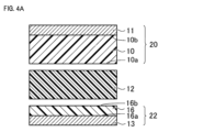
- FIG. 4A is a diagram illustrating a method for manufacturing a circuit board according to the third embodiment.
- FIG. 4B is a diagram illustrating a method for manufacturing a circuit board according to the third embodiment.
- FIG. 4A is a diagram illustrating a method for manufacturing a circuit board according to the third embodiment.
- FIG. 4B is a diagram illustrating a method for manufacturing a circuit board according to the third embodiment.
- FIG. 4C is a diagram illustrating a method for manufacturing a circuit board according to the third embodiment.
- FIG. 5 is a schematic cross-sectional view of a circuit board according to the fourth embodiment.
- FIG. 6 is a schematic cross-sectional view of a circuit board according to the fifth embodiment.
- FIG. 7A is a diagram illustrating a method for manufacturing a circuit board according to the fifth embodiment.
- FIG. 7B is a diagram illustrating a method for manufacturing a circuit board according to the fifth embodiment.
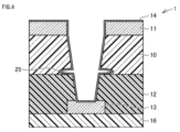
- FIG. 8 is a diagram for explaining the gouging.
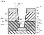
- FIG. 9 is a diagram for explaining a method for measuring the length of the hollow.
- the circuit board 1 includes an adhesive layer 12 (corresponding to a bonding sheet) mainly composed of polypropylene.
- the inner wall surfaces of the fluororesin layer 10 and the adhesive layer 12 are plated to form a via hole.
- the portion of the gouging 25 is difficult to plate.
- a portion of the via hole is insufficiently plated, which tends to reduce the reliability of the circuit board.
- the present disclosure aims to provide a circuit board in which a fluororesin layer and an adherend layer are bonded by pressing at low temperature.
- the present disclosure aims to provide a circuit board in which the occurrence of gouging near the interface between the fluororesin layer and the adhesive layer is suppressed when a through hole is formed penetrating the fluororesin layer and the adhesive layer.
- the present disclosure it is possible to provide a circuit board in which a fluororesin layer and an adherend layer are bonded by pressing at a low temperature.
- the present disclosure can provide a circuit board in which, when a through hole is formed penetrating the fluororesin layer and the adhesive layer, the occurrence of gouging near the interface between the fluororesin layer and the adhesive layer is suppressed.
- the circuit board of the present disclosure is A fluororesin layer; An adherend layer; An adhesive layer that adheres the fluororesin layer and the adherend layer,
- the fluororesin layer contains polytetrafluoroethylene and a first inorganic filler, The content of the first inorganic filler in the fluororesin layer is 50% by volume or more and 66% by volume or less,
- the adhesive layer includes a resin and a second inorganic filler, The content of the fluororesin in the resin is 5% by mass or less, The content of the second inorganic filler in the adhesive layer is 29 vol% or more and 47 vol% or less,
- the circuit board has a through hole formed therethrough that penetrates the fluororesin layer and the adhesive layer.
- the present disclosure it is possible to provide a circuit board in which a fluororesin layer and an adherend layer are bonded by pressing at low temperature. Furthermore, according to the present disclosure, it is possible to provide a circuit board in which the occurrence of gouging near the interface between the fluororesin layer and the adhesive layer is suppressed even when a through hole is formed that penetrates the fluororesin layer and the adhesive layer.
- low temperature means a temperature of 180°C or lower.
- the first inorganic filler may contain silica. This can reduce the thermal expansion coefficient of the fluororesin layer.
- the thermal expansion coefficient of the fluororesin layer is the linear expansion coefficient in the thickness direction of the fluororesin layer (thermal expansion coefficient for the length along an axis perpendicular to the layer surface of the fluororesin layer).
- the second inorganic filler may contain silica. This can further suppress the occurrence of gouging.
- the second inorganic filler may contain boron nitride. This can further suppress the occurrence of gouging.
- At least one of the inner wall surface of the fluororesin layer that defines a portion of the through hole and the inner wall surface of the adhesive layer that defines a portion of the through hole may have a recess, and the length of the recess may be less than 25 ⁇ m. This improves the reliability of the circuit board.
- the ratio A/B of the elastic modulus A at 160°C to the elastic modulus B at 20°C of the adhesive layer may be 0.08 or less. This improves the adhesion between the fluororesin layer and the metal layer at low temperatures.
- the resin may contain a polyolefin or a polystyrene-based elastomer. This improves the adhesion between the fluororesin layer and the metal layer at low temperatures.
- the adherend layer may include a first metal layer and a first resin layer, and the first metal layer may be provided on a surface of the first resin layer facing the fluororesin layer.
- the adherend layer may include a first metal layer and a first resin layer, and the first resin layer may be provided on a surface of the first metal layer facing the fluororesin layer. This allows a circuit to be formed on the first metal layer.
- the fluororesin layer includes a first main surface facing the adhesive layer and a second main surface opposite to the first main surface
- the circuit board may further include a second metal layer provided on the second main surface.
- connection portion electrically connecting the first metal layer and the second metal layer is further provided,
- the connection portion may be formed in the through hole.
- the first metal layer may be formed in an area that overlaps with the through hole when viewed from a direction perpendicular to the second main surface. This allows the shape of the connection portion to be precisely defined.
- the second metal layer may be formed in an area that overlaps with the through hole when viewed from a direction perpendicular to the first main surface. This allows the shape of the connection portion to be precisely defined.
- a method for producing a circuit board according to the present disclosure is a method for producing the circuit board according to any one of (1) to (13) above, comprising the steps of:
- the method for manufacturing a circuit board includes a step of maintaining a laminate in which the fluororesin layer, the adhesive layer, and the adherend layer are laminated in this order at a temperature of 180° C. or less to soften the adhesive layer, thereby adhering the fluororesin layer and the adherend layer to each other.
- the present disclosure it is possible to provide a circuit board in which a fluororesin layer and an adherend layer are bonded by pressing at low temperatures. Furthermore, according to the present disclosure, it is possible to provide a circuit board in which the occurrence of gouging near the interface between the fluororesin layer and the adhesive layer is suppressed, even when a through hole is formed that penetrates the fluororesin layer and the adhesive layer.
- a method for manufacturing a circuit board includes: A step of preparing a fluororesin laminate including a fluororesin layer including a first main surface and a second main surface opposite to the first main surface, and a second metal layer provided on the second main surface; A step of preparing a first resin laminate including a first resin layer including a third main surface and a fourth main surface opposite to the third main surface, and a first metal layer provided on the third main surface; providing an adhesive layer; a step of laminating the fluororesin laminate, the adhesive layer, and the first resin laminate in this order such that the first main surface is in contact with the adhesive layer, and maintaining the adhesive layer at a temperature of 180° C.
- the fluororesin layer contains polytetrafluoroethylene and a first inorganic filler, The content of the first inorganic filler in the fluororesin layer is 50% by volume or more and 66% by volume or less,
- the adhesive layer includes a resin and a second inorganic filler, The content of the fluororesin in the resin is 5% by mass or less, In the method for producing a circuit board, the adhesive layer has a content of the second inorganic filler of 29 volume % or more and 47 volume % or less.
- the present disclosure it is possible to provide a circuit board in which a fluororesin layer and an adherend layer are bonded by pressing at low temperatures. Furthermore, according to the present disclosure, it is possible to provide a circuit board in which the occurrence of gouging near the interface between the fluororesin layer and the adhesive layer is suppressed, even when a through hole is formed that penetrates the fluororesin layer and the adhesive layer.
- the step of preparing the first resin laminate may further include a step of forming a first circuit in the first resin laminate by etching at least a part of the first metal layer. This allows the first circuit to be embedded in the adhesive layer.
- the step of preparing the fluororesin laminate may further include a step of forming a second circuit in the fluororesin laminate by etching at least a part of the second metal layer. In this way, the wiring density of the circuit board can be increased by forming the second circuit.
- the step of forming the first laminate may further include a step of forming a second circuit in the fluororesin laminate by etching at least a part of the second metal layer. In this way, the wiring density of the circuit board can be increased by forming the second circuit.
- the through hole may be formed by laser processing. This allows the through hole to be formed with high precision.
- At least one of the inner wall surface of the fluororesin layer and the inner wall surface of the adhesive layer has a hollow,
- the length of the recess may be less than 25 ⁇ m, which improves the reliability of the circuit board.
- the expression "from A to B" means a range from the upper limit to the lower limit (greater than or equal to A and less than or equal to B). If no unit is stated for A, and a unit is stated only for B, the units for A and B are the same.
- the compound when a compound is represented by a chemical formula and the atomic ratio is not limited, the compound includes compounds with any conventionally known atomic ratio and is not limited to compounds within the stoichiometric range.
- the lower limit and upper limit of a numerical range are each one or more numerical values
- a combination of any one numerical value stated as the lower limit and any one numerical value stated as the upper limit is deemed to be disclosed.
- a1, b1, and c1 are stated as the lower limit and a2, b2, and c2 are stated as the upper limit
- a1 to a2, a1 to b2, a1 to c2, b1 to a2, b1 to b2, b1 to c2, c1 to a2, c1 to b2, and c1 to c2 are deemed to be disclosed.
- the circuit board 1 of embodiment 1 includes a fluororesin layer 10, an adherend layer 17, and an adhesive layer 12 that adheres the fluororesin layer 10 and the adherend layer 17.
- the fluororesin layer 10 includes polytetrafluoroethylene and a first inorganic filler.
- the content of the first inorganic filler in the fluororesin layer 10 is 50% by volume or more and 66% by volume or less.
- the adhesive layer 12 includes a resin and a second inorganic filler.
- the content of the fluororesin in the resin is 5% by mass or less.
- the content of the second inorganic filler in the adhesive layer 12 is 29% by volume or more and 47% by volume or less.
- the circuit board 1 includes a through hole penetrating the fluororesin layer 10 and the adhesive layer 12.
- the circuit board 1 of embodiment 1 is a circuit board in which the fluororesin layer 10 and the adherend layer 17 are adhered by the adhesive layer 12 by pressing at low temperature.
- the circuit board 1 of embodiment 1 can have excellent reliability.
- the circuit board is not limited to a board in which a circuit is formed by processing a metal layer of a substrate.
- the circuit board of this disclosure includes a laminate formed by bonding a substrate or another circuit board to a circuit board using a bonding sheet, and a laminate provided with connection holes such as via holes.
- the circuit board 1 of the first embodiment includes a fluororesin layer 10, an adherend layer 17, and an adhesive layer 12 that adheres the fluororesin layer 10 and the adherend layer 17.
- the fluororesin layer 10 includes a first main surface 10a facing the adhesive layer 12 and a second main surface 10b opposite to the first main surface 10a.
- the adherend layer 17 includes a first resin layer 16 and a first metal layer 13 provided on a part of the surface of the first resin layer 16.
- the first resin layer 16 may be a laminate including a layer such as a metal layer, a glass cloth layer, or a nonwoven fabric layer in addition to the resin layer.
- the resin layer may include an inorganic filler. As shown in FIG. 1, the first main surface 10a may be adjacent to the adhesive layer 12.
- the first A surface 13a of the first metal layer 13 is the surface opposite to the surface of the first metal layer 13 that is in contact with the first resin layer 16.
- the first B surface 12a of the adhesive layer 12 is the surface opposite to the surface of the adhesive layer 12 that is in contact with the fluororesin layer 10.
- the first A surface 13a is in contact with the first B surface 12a.
- At least a portion of the first metal layer 13 is embedded in the adhesive layer 12.
- the third main surface 16a of the first resin layer 16 is the surface facing the first metal layer 13. The area of the third main surface 16a where the first metal layer 13 is not provided is in contact with the adhesive layer 12.
- the circuit board 1 further includes a second metal layer 11 provided on the second main surface 10b of the fluororesin layer 10.
- the second metal layer 11 is made of metal.
- the fluororesin layer 10 and the second metal layer 11 may be in contact with each other.
- the fluororesin layer 10 and the second metal layer 11 may be bonded to each other by disposing a thin adhesive film (not shown) between the fluororesin layer 10 and the second metal layer 11.
- the circuit board 1 further includes a connection portion 14.
- the connection portion 14 is made of metal and electrically connects the first metal layer 13 and the second metal layer 11.
- a through hole is formed in the circuit board 1, penetrating the fluororesin layer 10 and the adhesive layer 12. That is, the fluororesin layer 10 and the adhesive layer 12 have a through hole penetrating the fluororesin layer 10 and the adhesive layer 12.
- the connection portion 14 is formed in the through hole. More specifically, the connection portion 14 is formed on the inner wall surface of the fluororesin layer 10 that defines a part of the through hole and on the inner wall surface that defines a part of the adhesive layer 12.
- the first metal layer 13 defines the bottom surface of the through hole, and the connection portion 14 is also formed on the bottom surface.
- the second metal layer 11 When the circuit board 1 is viewed from a direction perpendicular to the second main surface 10b, the second metal layer 11 is not formed in the area that overlaps with the through hole.
- the second metal layer 11 has an opening that leads to the through hole.
- the first metal layer 13 When the circuit board 1 is viewed from a direction perpendicular to the second main surface 10b, the first metal layer 13 is formed in the area that overlaps with the through hole.
- the first metal layer 13 is the via bottom that fills the through hole.
- the cross-sectional area of the through hole increases continuously from the first metal layer 13 to the second metal layer 11.
- the cross-sectional area of the through hole is the cross-sectional area when viewed in a cross section perpendicular to the direction from the first metal layer 13 to the second metal layer 11.
- the fluororesin layer contains polytetrafluoroethylene and a first inorganic filler.
- Polytetrafluoroethylene has a small dielectric constant and a small dielectric loss tangent. Therefore, a circuit board using the fluororesin layer as an insulating layer has good high frequency characteristics.
- the volumetric content of the first inorganic filler in the fluororesin layer is 50% by volume or more and 66% by volume or less. This provides excellent dimensional stability due to the small thermal expansion coefficient of the fluororesin layer. In addition, the electrical connection reliability of the connection portion provided on the inner wall surface of the fluororesin layer is excellent.
- the lower limit of the content of the first inorganic filler in the fluororesin layer is 50% by volume, or may be 60% by volume or 63% by volume, from the viewpoint of reducing the thermal expansion coefficient.
- the thermal expansion coefficient of the fluororesin layer is small, if the content is 60% by volume or more, the thermal expansion coefficient is further reduced, and if the content is 63% by volume or more, the thermal expansion coefficient is further reduced.
- the upper limit of the content of the first inorganic filler in the fluororesin layer is 66% by volume or more, or may be 65% by volume. If the content of the first inorganic filler in the fluororesin layer is 66% by volume or less, the electrical connection stability of the connection portion is excellent, and if the content is 65% by volume or less, the electrical connection stability of the connection portion is further improved.
- the content of the first inorganic filler in the fluororesin layer may be 60% by volume or more and 66% by volume or less, or 63% by volume or more and 65% by volume or less.
- the method for measuring the volumetric content of the first inorganic filler in the fluororesin layer is as follows:
- the circuit board is cut by argon ion polishing to expose the cross section of the fluororesin layer.
- the cross section is a plane perpendicular or parallel to the lamination surface of the circuit board. If the cross section is a plane parallel to the lamination surface of the circuit board, the area of the cross section is likely to be large. If the cross section is a plane perpendicular to the lamination surface, the cross section is easily formed.
- the cross section of the fluororesin layer is observed at 10,000 times magnification using a high-resolution scanning electron microscope (SEM) (SU8020 manufactured by Hitachi High-Tech Corporation) at a low acceleration voltage to obtain an SEM image.
- SEM scanning electron microscope
- a rectangular measurement area of 8 ⁇ m x 12 ⁇ m is provided in the SEM image.
- the area-based content (area percentage) of the first inorganic filler is measured.
- the area percentage measurement is performed by extracting the first inorganic filler portion using multi-value image analysis processing software.
- the area percentage of the first inorganic filler is measured for 30 different measurement areas, and the average area percentage is calculated.
- the average area percentage of the first inorganic filler is calculated for a total of 40 measurement areas obtained by adding 10 new measurement areas whose area percentages have not yet been measured to the measurement areas whose area percentages have already been measured. If the difference between the average area percentage before the addition of the 10 measurement areas and the average area percentage of the measurement areas after the addition of the 10 measurement areas is within 1%, the average area percentage of the measurement areas after the addition is taken as the volumetric content of the first inorganic filler in the fluororesin layer. If the difference is greater than 1%, 10 measurement areas whose area percentages have not yet been measured are added, and the average area percentage of the measurement areas after the addition is calculated. This operation is repeated until the difference before and after the addition of the measurement areas is within 1%. The average area percentage when the difference before and after the addition of the measurement areas is within 1% is taken as the volumetric content of the first inorganic filler in the fluororesin layer.
- the mass-based content of the first inorganic filler in the fluororesin layer may be 50% by mass or more and 67% by mass or less. This reduces the thermal expansion coefficient of the fluororesin layer, resulting in excellent dimensional stability. In addition, the electrical connection reliability of the connection portion provided on the inner wall surface of the fluororesin layer is excellent.
- the lower limit of the content of the first inorganic filler in the fluororesin layer may be 50% by mass, 60% by mass, or 63% by mass from the viewpoint of reducing the thermal expansion coefficient.
- the thermal expansion coefficient of the fluororesin layer is reduced, if the content is 60% by mass or more, the thermal expansion coefficient is further reduced, and if the content is 63% by mass or more, the thermal expansion coefficient is further reduced.
- the upper limit of the content of the first inorganic filler in the fluororesin layer may be 67% by mass or more and 66% by mass. If the content of the first inorganic filler in the fluororesin layer is 67% by mass or less, the electrical connection stability of the connection portion is excellent, and if the content is 67% by mass or less, the electrical connection stability of the connection portion is even more excellent.
- the content of the first inorganic filler in the fluororesin layer may be 50% by mass or more and 67% by mass or less, 60% by mass or more and 66% by mass or less, or further 63% by mass or more and 65% by mass or less.
- the method for measuring the mass-based content of the first inorganic filler in the fluororesin layer is as follows. Using a thermogravimetry and differential scanning calorimeter (TG-DSC), the fluororesin layer is heated under a nitrogen atmosphere, and the temperature of the fluororesin layer is increased from 30°C to 700°C at 20°C/min. The initial weight of the fluororesin layer and the recovered weight of the recovered material after heating are measured. The ratio of the recovered weight to the initial weight is the mass-based content of the first inorganic filler in the fluororesin layer.
- TG-DSC thermogravimetry and differential scanning calorimeter
- the first inorganic filler may be a nonmetallic inorganic filler and may contain silica.
- Silica is inexpensive and easily available.
- the dielectric tangent of silica is smaller than that of many other inorganic fillers. Since the dielectric constant of silica is close to that of fluororesin, even if the first inorganic filler contains a large amount of silica, the dielectric constant of the first inorganic filler does not change significantly.
- the silica content of the first inorganic filler may be 80 mass% or more, 90 mass% or more, or 92 mass% or more from the viewpoint of reducing the decrease in the dielectric tangent of the fluororesin layer.
- the upper limit of the silica content of the first inorganic filler may be 100 mass%.
- the silica content of the first inorganic filler may be 80 mass% or more and 100 mass% or less, 90 mass% or more and 100 mass% or less, or 92 mass% or more and 100 mass% or less from the viewpoint of suppressing the decrease in the dielectric tangent of the fluororesin layer.
- the method for measuring the mass-based silica content of the first inorganic filler in the fluororesin layer is as follows. First, the weight of the recovered material obtained in the above-described method for measuring the mass-based silica content of the first inorganic filler in the fluororesin layer is measured. Using the recovered material, the silicon (Si) content of the recovered material is measured by inductively coupled plasma (ICP) analysis. Assuming that silica has a composition of SiO2 , the silica content of the recovered material is calculated from the silicon content. This content is the mass-based silica content of the first inorganic filler in the fluororesin layer.
- ICP inductively coupled plasma
- the silica in the first inorganic filler may be a natural product or a synthetic product.
- the silica in the first inorganic filler may be crystalline or amorphous.
- the silica in the first inorganic filler may be silica produced by a dry process or silica produced by a wet process. From the standpoint of availability and quality, the silica in the first inorganic filler may be synthetic silica produced by a dry process.
- the silica in the first inorganic filler may contain spherical silica. This improves processability, such as hole drilling, in the manufacturing process of the circuit board.
- the content of spherical silica in the silica may be 80% by mass or more and 100% by mass or less, 90% by mass or more and 100% by mass or less, or 95% by mass or more and 100% by mass or less.
- spherical silica refers to silica with a sphericity of 0.80 or more.
- the average particle size of the spherical silica may be 0.2 ⁇ m or more and 7.0 ⁇ m or less. This means that the fluororesin layer has a large breaking elongation, excellent mechanical strength, and excellent processability such as cutting and perforation.
- the lower limit of the average particle size of the spherical silica may be 0.2 ⁇ m, 0.5 ⁇ m, or 1.0 ⁇ m from the viewpoint of mechanical strength such as breaking elongation.
- the mechanical strength of the fluororesin layer is excellent, if it is 0.5 ⁇ m or more, the mechanical strength of the fluororesin layer is even better, and if it is 1.0 ⁇ m or more, the mechanical strength of the fluororesin layer is even better.
- the upper limit of the average particle size of the spherical silica may be 7.0 ⁇ m, 5.0 ⁇ m, or 3.0 ⁇ m from the viewpoint of processability such as cutting and perforation.
- the average particle size of the spherical silica is 7.0 ⁇ m or less, the processability of the fluororesin layer is excellent, if it is 5.0 ⁇ m or less, the processability of the fluororesin layer is even better, and if it is 3.0 ⁇ m or less, the processability of the fluororesin layer is even better.
- the average particle size of the spherical silica may be 0.2 ⁇ m or more and 7.0 ⁇ m or less, 0.5 ⁇ m or more and 5.0 ⁇ m or less, or 1.0 ⁇ m or more and 3.0 ⁇ m or less.
- the average particle size of spherical silica is the average particle size of primary particles.
- the average particle size is expressed as the mode diameter of the volumetric particle size distribution.
- the method for measuring the average particle size of spherical silica in the fluororesin layer is as follows.
- the fluororesin layer is heated under a nitrogen atmosphere using a thermogravimetric differential thermal analyzer (TG-DSC) to increase the temperature of the fluororesin layer from 30°C to 700°C at 20°C/min to obtain a recovered material.
- the recovered material contains silica.
- the recovered material is observed with a SEM. 100 silica particles are randomly selected, the particle size is measured to determine the particle size distribution, and the average particle size is calculated.
- the first inorganic filler may contain titanium oxide. Since titanium oxide has a large dielectric constant, the dielectric constant of the fluororesin layer can be adjusted by adding a small amount of titanium oxide to the first inorganic filler.
- the titanium oxide content of the first inorganic filler may be 1 mass% or more, or 2 mass% or more.
- the upper limit of the titanium oxide content of the first inorganic filler may be 20 mass% or 10 mass%.
- the titanium oxide content of the first inorganic filler may be 1 mass% or more and 20 mass% or less, or 2 mass% or more and 10 mass% or less.
- the method for measuring the mass-based titanium oxide content of the first inorganic filler in the fluororesin layer is as follows. First, the weight of the recovered material obtained in the method for measuring the mass-based content of the first inorganic filler in the fluororesin layer described above is measured. The recovered material is used to measure the titanium (Ti) content in the recovered material by ICP analysis. Assuming that the titanium oxide has a composition of TiO2 , the titanium oxide content in the recovered material is calculated from the titanium content. This content is the mass-based titanium oxide content of the first inorganic filler.
- the first inorganic filler can contain both silica and titanium oxide. This allows the temperature stability of the dielectric constant to be improved, since the dielectric constant of titanium oxide has temperature change characteristics opposite to those of the dielectric constant of silica.
- the first inorganic filler may contain nonmetallic inorganic fillers other than silica and titanium oxide (hereinafter, also referred to as "other inorganic fillers"), so long as the effect of the present disclosure is not impaired.
- other inorganic fillers include aluminum oxide, magnesium oxide, calcium oxide, talc, barium sulfate, boron nitride, zinc oxide, potassium titanate, glass, and mica.
- One type of these inorganic fillers may be used, or two or more types may be used.
- the fluororesin layer may be made of polytetrafluoroethylene, a first inorganic filler, and inevitable impurities.
- the fluororesin layer may contain a resin other than polytetrafluoroethylene (another fluororesin). That is, the fluororesin layer may be made of polytetrafluoroethylene, a first inorganic filler, another fluororesin, and inevitable impurities.
- the upper limit of the content of the other fluororesin may be 10 mass% or 5 mass%.
- the fluororesin layer may contain components other than polytetrafluoroethylene and the first inorganic filler, so long as the effects of the present disclosure are not impaired.
- the total of polytetrafluoroethylene, the first inorganic filler, other fluororesins and unavoidable impurities, and components that may be contained so long as the effects of the present disclosure are not impaired is taken as 100%, and the content of polytetrafluoroethylene, etc. is defined.
- the fluororesin layer does not have to contain glass cloth.
- a fluororesin layer that does not contain glass cloth is less likely to cause unevenness on the inner wall surface, and has excellent electrical connection reliability when a connection is formed on the inner wall surface.
- the lower limit of the average thickness of the fluororesin layer may be 20 ⁇ m, 40 ⁇ m, or 60 ⁇ m. If the average thickness is less than 20 ⁇ m, the mechanical strength may be insufficient. In addition, the effect of dimensional errors on the high-frequency characteristics of the circuit board may be large, which may make it difficult to design the circuit and manufacture the circuit components.
- the upper limit of the average thickness of the fluororesin layer may be 500 ⁇ m, 300 ⁇ m, or 150 ⁇ m. If the average thickness exceeds 500 ⁇ m, the thickness of the circuit board may be too large. In addition, if flexibility is required for the circuit board, the flexibility may be insufficient.
- the average thickness of the fluororesin layer may be 20 ⁇ m or more and 500 ⁇ m or less, 40 ⁇ m or more and 300 ⁇ m or less, or 60 ⁇ m or more and 150 ⁇ m or less.
- average thickness refers to the distance between the average line of the interface close to the front surface of the circuit board and the average line of the interface close to the back surface in a cross section cut in the thickness direction of the object.
- the “average line” is an imaginary line drawn along the interface such that the total area of the peaks (total area above the imaginary line) and the total area of the valleys (total area below the imaginary line) defined by the interface and this imaginary line are equal.
- the average thickness of each layer described below is defined in the same way.
- the upper limit of the difference between the maximum and minimum thicknesses of the fluororesin layer may be 10 ⁇ m, 5 ⁇ m, or 2 ⁇ m. If the difference is 10 ⁇ m or less, 5 ⁇ m or less, or 2 ⁇ m or less, circuit design and manufacture of circuit components become easier.
- the maximum and minimum thicknesses of the fluororesin layer are measured using an outside micrometer MDH-25MB manufactured by Mitutoyo Corporation, with the terminal surface of the measurement terminal as the "plane".
- ⁇ Adhesive Layer> In order to reduce the transmission loss of the substrate, it is conceivable to use a fluororesin for the adhesive layer, in the same way as the dielectric layer of the substrate. However, since fluororesin has a high softening temperature, a press capable of pressing at high temperatures is required. In addition, since it takes time to heat up and cool down, productivity decreases. Furthermore, when the fluororesin is cooled to room temperature and changed from the softened state to the hardened state, thermal shrinkage is large, and dimensional stability is poor. For this reason, there is a demand for an adhesive layer that is mainly made of a resin with a small dielectric tangent and can be bonded at low temperatures.
- the adhesive layer includes a resin and a second inorganic filler.
- the circuit board of the first embodiment includes a laminate in which the adhesive layer and the above-mentioned fluororesin layer are bonded together in contact with each other. Even when a through hole is formed through the fluororesin layer and the adhesive layer, the circuit board suppresses the occurrence of gouging near the interface between the fluororesin layer and the adhesive layer.
- the adhesive layer has excellent adhesive strength to both the fluororesin layer and the adherend layer. Thus, the reliability of the circuit board of the first embodiment is improved.
- the fluororesin content of the resin of the adhesive layer is 5 mass% or less.
- the resin of the adhesive layer has a reduced content of fluororesin with a high softening temperature. Thus, the adhesive layer can adhere the fluororesin layer and the adherend layer at low temperatures.
- the resin may contain a polyolefin or polystyrene-based elastomer. This has a small dielectric tangent, which reduces the transmission loss in the circuit, and a low softening temperature, which allows bonding at temperatures below 180°C.
- the polyolefin may be, for example, polyethylene or polypropylene.
- the polyolefin may be an acid-modified polyolefin. This is because acid-modified polyolefins have strong adhesive strength with the fluororesin layer and the metal layer. Acid-modified polyolefins are polyolefins that contain carboxyl groups.
- the lower limit of the polyolefin content of the resin may be 70 mass%, 80 mass%, or 90 mass%, from the viewpoint of lowering the softening temperature of the adhesive layer and obtaining good mechanical strength.
- the upper limit of the polyolefin content of the resin may be 100 mass% or 95 mass%.
- the polyolefin content of the resin may be 70 mass% or more and 100 mass% or less, 80 mass% or more and 97 mass% or less, or 90 mass% or more and 95 mass% or less.
- the lower limit of the acid-modified polyolefin content of the resin may be 70 mass%, 80 mass%, or 90 mass%, from the viewpoint of lowering the softening temperature of the adhesive layer and obtaining good mechanical strength.
- the upper limit of the acid-modified polyolefin content of the resin may be 100 mass% or 95 mass%.
- the acid-modified polyolefin content of the resin may be 70 mass% or more and 100 mass% or less, 80 mass% or more and 97 mass% or less, or 90 mass% or more and 95 mass% or less.
- polystyrene-based elastomers examples include styrene-ethylene-butylene-styrene block copolymer (SEBS), styrene-ethylene-propylene-styrene copolymer (SEPS), and styrene-ethylene-ethylene-propylene-styrene block copolymer (SEEPS).
- SEBS styrene-ethylene-butylene-styrene block copolymer
- SEPS styrene-ethylene-propylene-styrene copolymer
- SEEPS styrene-ethylene-ethylene-propylene-styrene block copolymer
- the lower limit of the polystyrene-based elastomer content of the resin may be 50 mass%, 55 mass%, or 60 mass%, from the viewpoint of lowering the softening temperature of the adhesive layer and obtaining good mechanical strength.
- the upper limit of the polystyrene-based elastomer content of the resin may be 100 mass% or 80 mass%.
- the polystyrene-based elastomer content of the resin may be 50 mass% or more and 100 mass% or less, 55 mass% or more and 90 mass% or less, or 60 mass% or more and 80 mass% or less.
- the adhesive layer may contain a resin (other resin) other than polyolefin and polystyrene-based elastomer.
- the other resin is, for example, polyphenylene ether.
- the upper limit of the content of other resins may be 30 mass%, 20 mass%, or 10 mass% if the resin is a polyolefin. In the adhesive layer, the upper limit of the content of other resins may be 50 mass%, 45 mass%, or 40 mass% if the resin is a polystyrene-based elastomer.
- the volumetric content of the second inorganic filler in the adhesive layer is 29% by volume or more and 47% by volume or less. This allows the length of the gouge to be smaller than 25 ⁇ m. Since the softening temperature of the adhesive layer is low, the large thermal expansion coefficient of the adhesive layer does not pose a problem. Therefore, the adhesive layer does not need to contain the second inorganic filler in order to reduce the thermal expansion coefficient of the adhesive layer.
- the lower limit of the content of the second inorganic filler in the adhesive layer may be 29% by volume, 33% by volume, or 38% by volume from the viewpoint of reducing the length of the gouge.
- the upper limit of the content of the second inorganic filler in the adhesive layer may be 47% by volume, 43% by volume, or 40% by volume from the viewpoint of maintaining a strong adhesive strength.
- the content of the second inorganic filler in the adhesive layer is 29% by volume or more and 47% by volume or less, 33% by volume or more and 43% by volume or less, or 38% by volume or more and 40% by volume or less.
- the method for measuring the volumetric content of the second inorganic filler in the adhesive layer is as follows.
- the circuit board is cut by argon ion polishing to expose the cross section of the adhesive layer.
- the cross section is a plane perpendicular to the laminated surface of the circuit board or a perpendicular plane. If the cross section is a plane parallel to the laminated surface of the circuit board, the area of the cross section is likely to be large. If the cross section is a plane perpendicular to the laminated surface, the cross section is easily formed.
- the cross section of the adhesive layer is observed at 10,000 times magnification using a high-resolution scanning electron microscope (SEM) (SU8020 manufactured by Hitachi High-Tech Corporation) at a low acceleration voltage to obtain an SEM image.
- SEM scanning electron microscope
- a rectangular measurement area of 5 ⁇ m x 12 ⁇ m is provided in the SEM image.
- the area-based content (area percentage) of the second inorganic filler is measured.
- the area percentage is measured by extracting the part of the second inorganic filler using multi-value image analysis processing software.
- the area percentage of the second inorganic filler is measured for 30 different measurement areas, and the average area percentage is calculated.
- the average area percentage of the second inorganic filler is calculated for a total of 40 measurement areas obtained by adding 10 new measurement areas whose area percentages have not yet been measured to the measurement areas whose area percentages have already been measured. If the difference between the average area percentages before the addition of the 10 measurement areas and the average area percentages of the measurement areas after the addition of the 10 measurement areas is within 1%, the average area percentages of the measurement areas after the addition are taken as the volumetric content of the second inorganic filler in the adhesive layer. If the difference is greater than 1%, 10 measurement areas whose area percentages have not yet been measured are added, and the average area percentages of the measurement areas after the addition are calculated. This operation is repeated until the difference before and after the addition of the measurement areas is within 1%. The average area percentages when the difference before and after the addition of the measurement areas is within 1% are taken as the volumetric content of the second inorganic filler in the adhesive layer.
- the mass-based content of the second inorganic filler in the adhesive layer may be 40% by mass or more and 70% by mass or less. This allows the length of the gouge to be smaller than 25 ⁇ m.
- the lower limit of the content of the second inorganic filler in the adhesive layer may be 40% by mass, 50% by mass, or 55% by mass.
- the upper limit of the content of the second inorganic filler in the adhesive layer may be 70% by mass, 67% by mass, or 63% by mass.
- the content of the second inorganic filler in the adhesive layer may be 40% by mass or more and 70% by mass or less, 50% by mass or more and 67% by mass or less, or 55% by mass or more and 63% by mass or less.
- the method for measuring the mass content of the second inorganic filler in the adhesive layer is as follows. Using a thermogravimetric differential scanning calorimeter (TG-DSC), the adhesive layer is heated under a nitrogen atmosphere, and the temperature of the adhesive layer is increased from 30°C to 700°C at 20°C/min. The initial weight of the adhesive layer and the recovered weight of the recovered material after heating are measured. The ratio of the recovered weight to the initial weight is the mass content of the second inorganic filler in the adhesive layer.
- TG-DSC thermogravimetric differential scanning calorimeter
- the absolute value Z of the difference between X and Y may be 0 or more and 17 or less, or may be 0 or more and 10 or less, or may be 0 or more and 7 or less. This allows the length of the gouge to be further reduced.
- the second inorganic filler may be a non-metallic inorganic filler and may contain silica.
- the specific gravity of silica is relatively small.
- the surface of silica is easy to treat, for example, with a silane coupling agent. Therefore, silica is easy to mix with the resin of the adhesive layer.
- Silica is inexpensive and easy to obtain.
- the silica content of the second inorganic filler may be 50% by mass or more and 100% by mass or less, 70% by mass or more and 100% by mass or less, or 90% by mass or more and 100% by mass or less.
- the method for measuring the mass-based silica content of the second inorganic filler in the adhesive layer is as follows. First, the recovered weight of the recovered material obtained in the method for measuring the mass-based silica content of the second inorganic filler in the adhesive layer described above is measured. Using the recovered material, the silicon (Si) content of the recovered material is measured by ICP analysis. Assuming that silica has a composition of SiO2 , the silica content of the recovered material is calculated from the silicon content. This content is the mass-based silica content of the second inorganic filler in the adhesive layer.
- the second inorganic filler may contain boron nitride. Since boron nitride has a low dielectric constant, even if the second inorganic filler contains a large amount of boron nitride, the dielectric constant of the adhesive layer does not change significantly. In addition, since boron nitride has a high thermal conductivity, the heat dissipation of the circuit board can be improved by having the second inorganic filler contain boron nitride. From the viewpoint of improving thermal conductivity, the content of boron nitride in the second inorganic filler may be 20 mass% or more, 40 mass% or more, or 60 mass% or more.
- the upper limit of the content of boron nitride in the second inorganic filler may be 100 mass%.
- the content of boron nitride in the second inorganic filler may be 20 mass% or more and 100 mass% or less, 40 mass% or more and 100 mass% or less, or 60 mass% or more and 100 mass% or less.
- the method for measuring the mass-based content of boron nitride in the second inorganic filler in the adhesive layer is as follows. First, the recovered weight of the recovered material obtained in the method for measuring the mass-based content of the second inorganic filler in the adhesive layer described above is measured. The recovered material is used to measure the boron content in the recovered material by ICP analysis. Assuming that boron nitride has a composition of BN, the boron nitride content in the recovered material is calculated from the boron content. This content is the mass-based content of boron nitride in the second inorganic filler in the adhesive layer.
- the second inorganic filler can contain both silica and boron nitride. This can suppress the occurrence of gouging and improve the heat dissipation of the circuit board. Furthermore, even if the second inorganic filler contains a large amount of silica and boron nitride, the dielectric constant of the adhesive layer does not change significantly.
- the second inorganic filler may contain nonmetallic inorganic fillers other than silica and boron nitride (hereinafter also referred to as "other inorganic fillers"), so long as the effect of the present disclosure is not impaired.
- other inorganic fillers include titanium nitride, aluminum oxide, magnesium oxide, calcium oxide, talc, barium sulfate, boron nitride, zinc oxide, potassium titanate, glass, and mica.
- One type of these other inorganic fillers may be used, or two or more types may be used.
- the adhesive layer may be composed of a resin, a second inorganic filler, and inevitable impurities.
- the adhesive layer may contain components other than the resin and the second inorganic filler, provided that the effects of the present disclosure are not impaired.
- components other than the resin and the second inorganic filler include flame retardants, flame retardant assistants, pigments, antioxidants, reflective agents, masking agents, lubricants, processing stabilizers, plasticizers, and foaming agents.
- the adhesive layer may contain one or more of these components.
- the upper limit of the content of the components in the adhesive layer may be 25% by mass, or 10% by mass.
- the ratio A/B of the adhesive layer's elastic modulus A at 160°C to its elastic modulus B at 20°C may be 0.08 or less. This allows the adhesive layer to fill between the circuits of the metal layer even when pressed at a temperature of 180°C or less. In addition, the adhesive layer and the metal layer are closely attached to each other, improving the adhesive strength between the adhesive layer and the metal layer. From the viewpoint of ensuring adhesiveness, the upper limit of the ratio A/B may be 0.08, 0.05, or 0.02. The lower limit of the ratio A/B may be 0.0001, 0.0005, or 0.001. The ratio A/B may be 0.0001 or more and 0.08 or less, 0.0005 or more and 0.05 or less, or 0.001 or more and 0.02 or less.
- the method for measuring the elastic modulus B of the adhesive layer at 20°C and the elastic modulus A at 160°C is as follows. Using a dynamic viscosity measuring (DMS) device, a vibration with a frequency of 1 Hz is applied to the bonding sheet constituting the adhesive layer while the bonding sheet is heated to increase the temperature of the bonding sheet from 15°C to 170°C at a rate of 10°C/min, and the elastic modulus at 20°C and 160°C is measured.
- DMS dynamic viscosity measuring
- the glass transition temperature of the adhesive layer may be 160°C or lower. This improves the adhesiveness when the fluororesin layer and the metal layer are pressed and bonded at a temperature of 180°C or lower.
- the upper limit of the glass transition temperature of the adhesive layer may be 160°C, 150°C, 120°C, or 100°C. If the glass transition temperature of the adhesive layer is 150°C or lower, the adhesiveness is further improved, if it is 120°C or lower, the adhesiveness is further improved, and if it is 100°C or lower, the adhesiveness is improved even more.
- the lower limit of the glass transition temperature of the adhesive layer may be 10°C. If the glass transition temperature of the adhesive layer is 10°C or higher, the heat resistance is improved.
- the glass transition temperature of the adhesive layer may be 30°C or higher and 160°C or lower, 30°C or higher and 150°C or lower, or 30°C or higher and 120°C or lower. If an adhesive layer has multiple glass transition temperatures, the glass transition temperature of the adhesive layer is determined to be the highest glass transition temperature among the glass transition temperatures attributable to resins whose volume ratio to the total volume of all resins is 10% or more.
- the method for measuring the glass transition temperature of the adhesive layer is as follows.
- a dynamic viscosity measurement (DMS) device is used to measure the glass transition temperature of the adhesive layer. While applying a vibration of 1 Hz frequency to the bonding that constitutes the adhesive layer, the bonding sheet is heated to increase the temperature of the bonding sheet from 15°C to 170°C at a rate of 10°C/min. Within this temperature range, the complex modulus of elasticity of the bonding sheet is measured, and the temperature at which tan ⁇ peaks, with the phase angle being ⁇ , is regarded as the glass transition temperature.
- DMS dynamic viscosity measurement
- the lower limit of the average thickness of the adhesive layer may be 5 ⁇ m, 20 ⁇ m, or 30 ⁇ m from the viewpoint of adhesion.
- the upper limit of the average thickness of the adhesive layer may be 100 ⁇ m, 70 ⁇ m, or 50 ⁇ m from the viewpoint of finishing the laminate thin.
- the average thickness of the adhesive layer may be 5 ⁇ m or more and 100 ⁇ m or less, 20 ⁇ m or more and 70 ⁇ m or less, or 30 ⁇ m or more and 50 ⁇ m or less.
- the average thickness of the adhesive layer may be greater than or equal to the thickness of the circuit from the viewpoint of filling between the circuits.
- the average thickness of the adhesive layer may be 10 ⁇ m or more thicker than the thickness of the circuit, or may be 20 ⁇ m or more thicker than the thickness of the circuit.
- the occurrence of gouging near the interface between the fluororesin layer 10 and the adhesive layer 12 is suppressed on the inner wall surface of the fluororesin layer and the inner wall surface of the adhesive layer. Even if gouging occurs in the fluororesin layer, the length of the gouging can be made very small.
- at least one of the inner wall surface of the fluororesin layer and the inner wall surface of the adhesive layer has a gouging. The length of the gouging may be less than 25 ⁇ m, less than 20 ⁇ m, or less than 15 ⁇ m.
- the inner wall surface of the fluororesin layer and the inner wall surface of the adhesive layer do not need to have a gouging.
- the circuit board 1 is cut along a plane including the central axis L1 of the through hole to expose a cross section of the laminate of the fluororesin layer 10 and the adhesive layer 12.
- the central axis L1 corresponds to a line connecting the center (geometric center) of the opening of the through hole in the second main surface 10b of the fluororesin layer 10 and the center (geometric center) of the opening of the through hole in the first B surface 12a of the adhesive layer 12.
- the interface between the fluororesin layer 10 and the adhesive layer 12 is defined as the interface P1.
- a straight line between the interface P1 and the fluororesin layer 10, parallel to the interface P1, and 10 ⁇ m away from the interface P1 is defined as the line P1F.
- a straight line between the interface P1 and the adhesive layer 12, parallel to the interface P1, and 10 ⁇ m away from the interface P1 is defined as the line P1B.
- a gouge in the region between the interface P1 and the line P1F, or in the region between the interface P1 and the line P1F is specified. In FIG. 9, the gouge 25 exists in the interface P1 and in the region between the interface P1 and the line P1F. When the interface has unevenness, the interface is defined by its average line.
- the "average line” refers to a virtual line drawn along the interface in the cross section, and refers to a line such that the total area of the mountains (total area above the virtual line) and the total area of the valleys (total area below the virtual line) partitioned by the interface and this virtual line are equal.
- the adherend layer 17 may include a first resin layer 16 and a first metal layer 13 provided on a part of the surface of the first resin layer 16.
- the adherend layer 17 includes a first metal layer 13 and a first resin layer 16.
- the first metal layer 13 is made of metal.
- the first metal layer 13 is provided so as to be closer to the first main surface 10a of the fluororesin layer 10 than the first resin layer 16.
- the positional relationship between the first resin layer 16 and the first metal layer 13 may be reversed.
- the first resin layer 16 may be provided so as to be closer to the first main surface 10a than the first metal layer 13.
- the first metal layer 13 forms an electrical circuit.
- the electrical circuit includes an antenna.
- the first metal layer may contain copper. Copper has low resistance and small transmission loss.
- the copper content of the first metal layer may be 90% by mass or more and 100% by mass or less, 95% by mass or more and 100% by mass or less, or 99% by mass or more and 100% by mass or less.
- the first metal layer may be a layer made of copper and unavoidable impurities.
- the first metal layer may contain a metal other than copper.
- metals other than copper include silver, nickel, cobalt, zinc, and chromium. One or more of these metals may be used.
- the average thickness of the first metal layer may be 1 ⁇ m or more, 5 ⁇ m or more, or 10 ⁇ m or more from the viewpoint of reducing electrical resistance.
- the upper limit of the average thickness of the first metal layer may be 100 ⁇ m, 70 ⁇ m, or 50 ⁇ m from the viewpoint of ease of manufacture.
- the average thickness of the first metal layer may be 1 ⁇ m or more and 100 ⁇ m or less, 5 ⁇ m or more and 70 ⁇ m or less, or 10 ⁇ m or more and 50 ⁇ m or less.
- the upper limit of the maximum height roughness Rz of the surface of the first metal layer facing the first resin layer may be 2 ⁇ m or 1 ⁇ m. If the maximum height roughness Rz is 2 ⁇ m or less, the unevenness of the area where the high frequency signal is concentrated due to the skin effect is small, so that the current tends to flow linearly. Therefore, the transmission loss can be suppressed, and the high frequency characteristics of the circuit board can be further improved.
- Maximum height roughness Rz refers to the maximum height roughness measured in accordance with JIS-B-0601 (1982). Specifically, the maximum height roughness Rz is measured using a laser microscope VK-X200 manufactured by Keyence Corporation.
- the first resin layer 16 may contain epoxy resin and glass cloth. This allows the circuit board to be manufactured at low cost.
- the dielectric tangent of the first resin layer 16 may be 0.01 or less, 0.005 or less, or 0.002 or less. This reduces the transmission loss of the first metal layer, resulting in excellent high-frequency characteristics.
- the first resin layer 16 may contain fluororesin and inorganic filler. This reduces the transmission loss of the first metal layer, resulting in excellent high-frequency characteristics.
- the second metal layer 11 forms an electrical circuit.
- the electrical circuit includes an antenna.
- the second metal layer 11 may contain copper. Copper has low resistance and small transmission loss.
- the copper content of the second metal layer 11 may be 90% by mass or more and 100% by mass or less, 95% by mass or more and 100% by mass or less, or 99% by mass or more and 100% by mass or less.
- the second metal layer may be a layer made of copper and unavoidable impurities.
- the second metal layer 11 may contain a metal other than copper.
- metals other than copper include silver, nickel, cobalt, zinc, and chromium. One of these metals may be used, or two or more of them may be used.
- the average thickness of the second metal layer 11 may be 1 ⁇ m or more, 5 ⁇ m or more, or 10 ⁇ m or more from the viewpoint of reducing electrical resistance.
- the upper limit of the average thickness of the second metal layer 11 may be 100 ⁇ m, 70 ⁇ m, or 50 ⁇ m from the viewpoint of ease of manufacture.
- the average thickness of the second metal layer 11 may be 1 ⁇ m or more and 100 ⁇ m or less, 5 ⁇ m or more and 70 ⁇ m or less, or 10 ⁇ m or more and 50 ⁇ m or less.
- connection portion 14 forms a via hole.
- the connection portion 14 is formed on the end face of the second metal layer 11 that defines a part of the through hole, the through hole vicinity region of the outer surface of the second metal layer 11, the inner wall surface of the fluororesin layer 10 and the adhesive layer 12, and the surface (first A surface 13a) of the first metal layer 13 that defines a part of the through hole and is adjacent to the adhesive layer.
- the formation location of the connection portion 14 is not limited to the form of FIG. 1.
- the connection portion 14 may be electrically connected to the first metal layer 13 and the second metal layer 11.
- the connection portion 14 may be formed in the through hole.
- connection portion 14 may be formed on the inner wall surface of the fluororesin layer 10 and the adhesive layer 12, the connection portion 14 adjacent to the fluororesin layer 10 may be in contact with at least a part of the second metal layer 11, and the connection portion 14 adjacent to the adhesive layer 12 may be in contact with at least a part of the first metal layer 13.
- connection may contain copper. This gives the connection a high electrical conductivity and reduces transmission loss.
- connection portion may contain a metal other than copper.
- metals other than copper include silver, nickel, cobalt, zinc, and chromium. One or more of these metals may be used.
- the average thickness of the connection part may be 1 ⁇ m or more, 5 ⁇ m or more, or 10 ⁇ m or more.
- the upper limit of the average thickness of the connection part may be 100 ⁇ m, 50 ⁇ m, or 30 ⁇ m.
- the average thickness of the connection part may be 1 ⁇ m or more and 100 ⁇ m or less, 5 ⁇ m or more and 50 ⁇ m or less, or 10 ⁇ m or more and 30 ⁇ m or less.
- the cross-sectional area of the through hole increases continuously from the first metal layer 13 to the second metal layer 11.
- the change in the cross-sectional area of the through hole is not limited to this.
- the cross-sectional area of the through hole may be constant or may decrease continuously from the first metal layer 13 to the second metal layer 11.
- the circuit board of the embodiment may include an adhesive film disposed between the fluororesin layer and the second metal layer.
- the adhesive film may improve the adhesion between the fluororesin layer and the second metal layer.
- the adhesive thin film may contain a fluororesin.
- the resin include perfluoroalkoxyalkane (PFA) and perfluoroethylenepropene copolymer (FEP).
- the average thickness of the thin adhesive film may be 3 ⁇ m or less, so as not to interfere with the function of the fluororesin layer.
- the method for manufacturing a circuit board according to the first embodiment includes a step of bonding the fluororesin layer and the adherend layer by maintaining a laminate in which a fluororesin layer, an adhesive layer, and an adherend layer are laminated in this order at a temperature of 180° C. or less to soften the adhesive layer. This prevents the occurrence of gouging near the interface between the fluororesin layer and the adhesive layer, even when a through hole is formed through the fluororesin layer and the adhesive layer.
- Embodiment 2 Manufacturing method of circuit board (1)
- a method for manufacturing a circuit board according to an embodiment of the present disclosure (hereinafter also referred to as “embodiment 2") will be described with reference to FIGS. 1, 2A, 2B, and 2C.
- the method for manufacturing the circuit board 1 according to the second embodiment includes the steps of: A step of preparing a fluororesin laminate 20 including a fluororesin layer 10 including a first main surface 10a and a second main surface 10b opposite to the first main surface 10a, and a second metal layer 11 provided on the second main surface 10b (hereinafter also referred to as a "first step") (see FIG.
- a step of preparing a first resin laminate 22 including a first resin layer 16 including a third main surface 16a and a fourth main surface 16b opposite to the third main surface 16a, and a first metal layer 13 provided on the third main surface 16a (hereinafter also referred to as a "second step") (see FIG. 2A);
- a step of preparing an adhesive layer 12 (hereinafter also referred to as a "third step") (see FIG.
- a step (hereinafter also referred to as a "fourth step") of laminating the fluororesin laminate 20, the adhesive layer 12, and the first resin laminate 22 in this order such that the first main surface 10a is in contact with the adhesive layer 12, and maintaining the adhesive layer 12 at a temperature of 180°C or less to soften the adhesive layer 12, thereby bonding the fluororesin laminate 20 and the first resin laminate 22 to obtain a first laminate 24 (see FIG. 2B ); a step of removing at least a part of the fluororesin layer 10 and at least a part of the adhesive layer 12 to form a through hole penetrating the fluororesin layer 10 and the adhesive layer 12 (hereinafter also referred to as a "fifth step”) (see FIG.
- connection portion 14 a connection portion 14 on an inner wall surface of the fluororesin laminate 20 that defines a part of the through hole and on an inner wall surface of the adhesive layer 12 that defines a part of the through hole to obtain a circuit board 1 (see FIG.
- the fluororesin layer 10 contains polytetrafluoroethylene and a first inorganic filler, The content of the first inorganic filler in the fluororesin layer 10 is 50% by volume or more and 66% by volume or less,
- the adhesive layer 12 includes a resin and a second inorganic filler, The fluororesin content of the resin is 5% by mass or less, In the method for producing a circuit board, the content of the second inorganic filler in the adhesive layer is 29 volume % or more and 47 volume % or less.
- the fluororesin layer 10, adhesive layer 12, first metal layer 13, second metal layer 11, first resin layer 16 and connection portion 14 can be the same as those in embodiment 1.
- steps 1, 2, 3, 4, 5 and 6 are described. The order of steps 1, 2 and 3 does not have to be in this order, and any of these steps may be performed first. Steps 1, 2 and 3 may be performed simultaneously. After steps 1, 2 and 3, steps 4, 5 and 6 are performed in this order.
- a fluororesin laminate 20 is prepared, which includes a fluororesin layer 10 including a first main surface 10a and a second main surface 10b opposite to the first main surface 10a, and a second metal layer 11 provided on the second main surface 10b.
- Examples of methods for providing the second metal layer 11 on the second main surface 10b include a method of thermocompression bonding the fluororesin layer 10 and the second metal layer 11 by high-temperature pressing, a method of bonding the fluororesin layer 10 and the second metal layer 11 by disposing a thin adhesive film between them, a method of depositing a metal constituting the second metal layer 11 on the fluororesin layer 10, and a method of plating a metal constituting the second metal layer 11 on the fluororesin layer 10.
- the first step can further include a step of forming a second circuit in the fluororesin laminate 20 by etching at least a part of the second metal layer 11.
- a method for etching at least a part of the second metal layer 11 include known etching methods such as a wet etching method in which a resist pattern is formed and then the laminate is immersed in a chemical solution containing an acid or alkali, and a dry etching method using an ion beam.
- a first resin laminate 22 is prepared, which includes a first resin layer 16 including a third main surface 16a and a fourth main surface 16b opposite the third main surface 16a, and a first metal layer 13 provided on the third main surface 16a.
- Methods for providing the first metal layer 13 on one main surface of the first resin layer 16 include, for example, a method of thermocompression bonding the first resin layer 16 and the first metal layer 13 using a high-temperature press, a method of placing a thin adhesive film between the first resin layer 16 and the first metal layer 13 and bonding them, a method of vapor-depositing the metal that constitutes the first metal layer 13 on the first resin layer 16, and a method of plating the metal that constitutes the first metal layer 13 on the first resin layer 16.
- the second step may further include a step of forming a first circuit in the first resin laminate 22 by etching at least a portion of the first metal layer 13.
- a method for etching at least a portion of the first metal layer 13 include known etching methods such as a wet etching method in which a resist pattern is formed and then the laminate is immersed in a chemical solution containing an acid or alkali, and a dry etching method using an ion beam.
- the adhesive layer 12 is prepared.
- ⁇ Fourth step> the fluororesin laminate 20, the adhesive layer 12, and the first resin laminate 22 are laminated in this order such that the first main surface 10a is in contact with the adhesive layer 12, and the adhesive layer 12 is kept at a temperature of 180° C. or less to soften the adhesive layer 12, thereby bonding the fluororesin laminate 20 and the first resin laminate 22 to obtain the first laminate 24.
- the first metal layer 13 is disposed so as to be in contact with the adhesive layer 12 during lamination.
- the temperature at which the adhesive layer is maintained may be 140°C or higher and 180°C or lower, or 160°C or higher and 180°C or lower. Heat may be applied to the adhesive layer while pressure is applied to the laminate of the fluororesin laminate 20, the adhesive layer 12, and the first resin laminate 22.
- the pressure may be 0.5 MPa or higher and 8 MPa or lower, 1 MPa or higher and 6 MPa or lower, or 3 MPa or higher and 5 MPa or lower.
- the time for which the adhesive layer is maintained at the above temperature and the above pressure is applied to the laminate may be 20 minutes or longer and 120 minutes or shorter.
- the fourth step may further include a step of forming a second circuit in the fluororesin laminate 20 by etching at least a portion of the second metal layer 11.
- a method of etching at least a portion of the second metal layer 11 include known etching methods such as a wet etching method in which a resist pattern is formed and then the laminate is immersed in a chemical solution containing an acid or alkali, and a dry etching method using an ion beam.
- the second circuit may be formed in the first step or the fourth step.
- ⁇ Fifth step> At least a portion of the fluororesin layer 10 and at least a portion of the adhesive layer 12 are removed to form through-holes passing through the fluororesin layer 10 and the adhesive layer 12 .
- a dry film is attached to the second metal layer 11, and the second metal layer 11 is etched by exposure.
- the dry film is then peeled off to form an opening in the second metal layer 11.
- a mask shielding layer
- laser processing is performed on the fluororesin layer 10 and the adhesive layer 12 through the opening.
- at least a portion of the fluororesin layer 10 and at least a portion of the adhesive layer 12 are removed, forming an opening in the second metal layer 11 and a through hole penetrating the fluororesin layer 10 and the adhesive layer 12.
- the second metal layer 11 may be a laser shielding layer.
- a CO2 laser may be used for the laser processing.
- a CO2 laser is used, it is easy to make the second metal layer 11 a laser shielding layer.
- the through hole does not penetrate the first metal layer 13 and is a blind via hole.
- the first metal layer 13 may be provided on the third main surface 16a of the first resin layer 16. In this way, the distance between the first metal layer 13 and the second metal layer 11 is small, so that wiring can be arranged at a high density. In this case, the circuit formed on the first metal layer 13 is embedded in the adhesive layer 12.
- the laser is reflected by the first metal layer 13 when a through hole is formed by laser processing. Therefore, the length of the gouge near the interface between the fluororesin layer 10 and the adhesive layer 12 is larger than that of a circuit board in which the laser is not reflected. According to the present disclosure, even in a circuit board in which the first metal layer is the via bottom of the blind via hole, the length of the gouge can be suppressed. Therefore, this disclosure is particularly effective for circuit boards in which the first metal layer is the via bottom of a blind via hole.
- a pretreatment process may be performed on the inner wall surfaces of the fluororesin layer 10 and the adhesive layer 12 to clean the inner wall surfaces.
- surface treatments include potassium permanganate treatment, alkali treatment, and plasma treatment.
- the alkaline treatment is a process in which the first laminate 24 is immersed in a strong alkaline solution such as potassium hydroxide to etch the surface layers of the inner walls of the fluororesin layer 10 and the adhesive layer 12.
- a strong alkaline solution such as potassium hydroxide
- Plasma treatment is a process in which plasma is brought into contact with the inner wall surfaces of the fluororesin layer 10 and the adhesive layer 12, thereby etching the surface of the inner wall surfaces.
- atmospheric pressure plasma treatment which is one example of plasma treatment, a plasma gas such as oxygen, nitrogen, hydrogen, argon, or ammonia is sprayed onto the inner wall surfaces.
- the entire surface of the first laminate 24 may be plasma treated by placing the first laminate 24 in a plasma gas atmosphere.
- plasma of an inert gas containing a compound having a hydrophilic group may be used.
- connection parts 14 are formed on the inner wall surfaces of the fluororesin laminate 20 and the adhesive layer 12 to obtain the circuit board 1 .
- connection portion 14 In forming the connection portion 14, first, an electroless plating layer is formed by electroless plating on the end face of the second metal layer 11 that defines part of the through hole, the area near the opening (through hole) on the outer surface of the second metal layer 11, the inner wall surface of the fluororesin layer 10, the inner wall surface of the adhesive layer 12, and the surface (first A surface 13a) of the first metal layer 13 near the adhesive layer that defines part of the through hole. Next, a plating layer is formed on the electroless plating layer by electrolytic plating. This plating layer is the connection portion 14.
- the circuit board 1 according to embodiment 3 includes a fluororesin layer 10, an adherend layer 17, and an adhesive layer 12 that adheres the fluororesin layer 10 and the adherend layer 17.
- the fluororesin layer 10 includes a first main surface 10a facing the adhesive layer 12 and a second main surface 10b opposite to the first main surface 10a.
- the adherend layer 17 includes a first resin layer 16 and a first metal layer 13 provided on at least a part of the surface of the first resin layer 16.
- the first resin layer 16 and the first metal layer 13 may be in contact with each other.
- a resin layer, a metal layer, an adhesive layer, or a laminate thereof may be disposed between the first resin layer 16 and the first metal layer 13 to bond the first resin layer 16 and the first metal layer 13.
- the circuit board 1 of the third embodiment includes a first resin layer 16 provided between the first metal layer 13 and the adhesive layer 12.
- the fourth main surface 16b of the first resin layer 16, which is far from the first metal layer 13, is in contact with the first B surface 12a of the adhesive layer 12, which is far from the fluororesin layer 10.
- the circuit board 1 further includes a second metal layer 11 provided on the second main surface 10b of the fluororesin layer 10.
- the fluororesin layer 10 and the second metal layer 11 may be in contact with each other.
- the fluororesin layer 10 and the second metal layer 11 may be bonded to each other by disposing a thin adhesive film (not shown) between the fluororesin layer 10 and the second metal layer 11.
- the circuit board 1 further includes a connection portion 14.
- the connection portion 14 is made of metal and electrically connects the first metal layer 13 and the second metal layer 11.
- the second metal layer 11, the fluororesin layer 10, the adhesive layer 12, and the first resin layer 16 include through holes penetrating them.
- the connection portion 14 is formed in the through holes. More specifically, the connection portion 14 is formed on the inner wall surface of the second metal layer 11, the inner wall surface of the fluororesin layer 10, the inner wall surface of the adhesive layer 12, and the inner wall surface of the first resin layer 16.
- the first metal layer 13 defines the bottom surface of the through hole, and the connection portion 14 is also formed on the bottom surface.
- the second metal layer 11 When the circuit board 1 is viewed from a direction perpendicular to the second main surface 10b of the fluororesin layer 10, the second metal layer 11 is not formed in the area overlapping the through hole.
- the second metal layer 11 has an opening that leads to the through hole.
- the first metal layer 13 When the circuit board 1 is viewed from a direction perpendicular to the second main surface 10b of the fluororesin layer 10, the first metal layer 13 is formed in the area overlapping the through hole.
- the first metal layer 13 is a via bottom that closes the through hole.
- the through hole that penetrates the fluororesin layer 10 and the adhesive layer 12 extends to the first resin layer 16.
- the connection portion 14 formed on the inner wall surface of the fluororesin layer 10 and the adhesive layer 12 also extends to the first resin layer 16.
- the cross-sectional area of the through hole increases continuously from the first metal layer 13 to the second metal layer 11.
- connection portion 14 can be the same as those in embodiment 1.
- circuit board 1 of embodiment 3 even if a through hole is formed through the fluororesin layer 10 and the adhesive layer 12, the occurrence of gouging of the fluororesin layer 10 near the interface between the fluororesin layer 10 and the adhesive layer 12 is suppressed. Therefore, the reliability of the circuit board 1 of embodiment 3 is improved.
- the method for manufacturing the circuit board 1 according to the third embodiment includes the steps of: A step of preparing a fluororesin laminate 20 including a fluororesin layer 10 including a first main surface 10a and a second main surface 10b opposite to the first main surface 10a, and a second metal layer 11 provided on the second main surface 10b (hereinafter also referred to as "step 1B") (see FIG. 4A); A step of preparing a first resin laminate 22 including a first resin layer 16 including a third main surface 16a and a fourth main surface 16b opposite to the third main surface 16a, and a first metal layer 13 provided on the third main surface 16a (hereinafter also referred to as "step 2B”) (see FIG.
- step 4A A step of preparing an adhesive layer 12 (hereinafter also referred to as “step 3B") (see FIG. 4A), a step of laminating the fluororesin laminate 20, the adhesive layer 12, and the first resin laminate 22 in this order such that the first main surface 10a is in contact with the adhesive layer 12, and maintaining the adhesive layer 12 at a temperature of 180° C. or less to soften the adhesive layer 12, thereby bonding the fluororesin laminate 20 and the first resin laminate 22 to obtain a first laminate 24 (hereinafter also referred to as “step 4B”) (see FIG.
- step 5B a step of removing at least a part of the fluororesin layer 10 and at least a part of the adhesive layer 12 to form a through hole penetrating the fluororesin layer 10 and the adhesive layer 12
- step 5B a step of removing at least a part of the fluororesin layer 10 and at least a part of the adhesive layer 12 to form a through hole penetrating the fluororesin layer 10 and the adhesive layer 12
- step 5C a step of forming connection portions 14 on the inner wall surfaces of the fluororesin laminate 20 and the adhesive layer 12 to obtain the circuit board 1 (see FIG.
- the fluororesin layer 10 contains polytetrafluoroethylene and a first inorganic filler, The content of the first inorganic filler in the fluororesin layer 10 is 50% by volume or more and 66% by volume or less,
- the adhesive layer 12 includes a resin and a second inorganic filler, The fluororesin content of the resin is 5% by mass or less, In the method for producing a circuit board, the content of the second inorganic filler in the adhesive layer is 29 volume % or more and 47 volume % or less.
- Steps 1B, 2B, and 3B of embodiment 3 can be the same as steps 1, 2, and 3 of embodiment 2, respectively.
- Step 4B of embodiment 3 can be the same as step 4 of embodiment 2, except that the first resin layer 16 is laminated so as to be in contact with the adhesive layer 12.
- step 5B of embodiment 3 at least a portion of the second metal layer 11, at least a portion of the fluororesin layer 10, at least a portion of the adhesive layer 12, and at least a portion of the first resin layer 16 are removed to form through holes that penetrate these layers.
- the method for forming the through hole can be the same as the method for forming the through hole in the fifth step of embodiment 2.
- the through hole does not penetrate the first metal layer 13 and is a blind via hole.
- a pretreatment process may be performed on the inner wall surfaces of the fluororesin layer 10, the adhesive layer 12, and the first resin layer.
- the pretreatment process may be the same as the pretreatment process of the second embodiment.
- connection parts 14 are formed on the end face of the second metal layer 11 that defines a portion of the through hole, the area near the opening (through hole) on the outer surface of the second metal layer 11, the inner wall surface of the fluororesin layer 10, the inner wall surface of the adhesive layer 12, the inner wall surface of the first resin layer 16, and the surface of the first metal layer 13 near the adhesive layer that defines a portion of the through hole, to obtain a circuit board 1.
- Connection parts 14 can be formed using electroless plating and electrolytic plating as in embodiment 2.
- FIG. 4 A circuit board according to an embodiment of the present disclosure (hereinafter also referred to as "embodiment 4") and a method for manufacturing the same will be described with reference to FIG. 5.
- the circuit board 1 of embodiment 4 is basically the same as the circuit board of embodiment 1.
- the circuit board of embodiment 4 differs from the circuit board of embodiment 1 in that it includes a filling portion 26 and a third metal layer 15.
- the filling portion 26 is filled in a through hole formed in the fluororesin layer 10 and the adhesive layer 12, and contacts the connection portion 14.
- the third metal layer 15 is provided on the first main surface 10a of the fluororesin layer 10 and embedded in the adhesive layer 12.
- the filling section 26 may contain resin. This can reduce stress on the connection section, such as stress caused by thermal expansion and contraction of the circuit board and external vibration, thereby improving the electrical connection reliability of the connection section.
- the filling section 26 containing resin can be easily formed, for example, by screen printing a paste-like material.
- the filled portion 26 may be formed by filling the through hole with metal using a plating process. This can reduce stress on the connection portion, such as stress caused by thermal expansion and contraction of the circuit board and external vibration, and can improve the reliability of the electrical connection at the connection portion. Filling using a plating process can be easily performed using the connection portion 14, so the filled portion 26 can be manufactured efficiently.
- the third metal layer 15 forms an electrical circuit.
- the third metal layer 15 can have the same configuration as the first metal layer 13.
- the method for manufacturing the circuit board of embodiment 4 is basically the same as the method for manufacturing the circuit board of embodiment 2. The differences from the method for manufacturing the circuit board of embodiment 2 are described below.
- a fluororesin layer 10 including a first main surface 10a and a second main surface 10b opposite the first main surface 10a, a second metal layer 11 provided on the second main surface 10b, and a third metal layer 15 provided on the first main surface 10a are prepared, and at least a portion of the second metal layer 11 and at least a portion of the third metal layer 15 are etched to form circuits on the second main surface 10b and the first main surface 10a.
- a step is performed in which the through holes in the fluororesin layer 10 and the adhesive layer 12 are filled with, for example, a resin to form a filled portion 26 that contacts the connection portion 14. This makes it possible to obtain the circuit board 1 of the fourth embodiment.
- the circuit board 1 of embodiment 5 includes a fluororesin layer 10, an adherend layer 17, and an adhesive layer 12 that adheres the fluororesin layer 10 and the adherend layer 17.
- the fluororesin layer 10 includes a first main surface 10a facing the adhesive layer 12 and a second main surface 10b opposite to the first main surface 10a.
- the adherend layer 17 is composed of a first metal layer 13 and a first resin layer 16.
- the fourth main surface 16b of the first resin layer 16 is in contact with the first B surface 12a of the adhesive layer 12, which is farther from the fluororesin layer 10.
- the circuit board 1 further includes a second metal layer 11 provided on the second main surface 10b of the fluororesin layer 10.
- the fluororesin layer 10 and the second metal layer 11 may be in contact with each other.
- the fluororesin layer 10 and the second metal layer 11 may be bonded to each other by disposing a thin adhesive film (not shown) between the fluororesin layer 10 and the second metal layer 11.
- the circuit board 1 further includes a connection portion 14.
- the connection portion 14 is made of metal and electrically connects the first metal layer 13 and the second metal layer 11.
- a through hole is formed in the circuit board 1, penetrating the first resin layer 16, the fluororesin layer 10, and the adhesive layer 12. That is, the first resin layer 16, the fluororesin layer 10, and the adhesive layer 12 have a through hole penetrating them.
- the connection portion 14 is formed in the through hole. More specifically, the connection portion 14 is formed near the through hole on the inner wall surface of the fluororesin layer 10, the inner wall surface of the adhesive layer 12, the inner wall surface of the first resin layer 16, and the end face and outer surface of the first metal layer.
- the second metal layer 11 defines the bottom surface of the through hole, and the connection portion 14 is also formed on the bottom surface.
- the first metal layer 13 When the circuit board 1 is viewed in a direction perpendicular to the first main surface 10a, the first metal layer 13 is not formed in the area that overlaps with the through hole.
- the first metal layer 13 has an opening that leads to the through hole.
- the second metal layer 11 When the circuit board 1 is viewed in a direction perpendicular to the first main surface 10a, the second metal layer 11 is formed in the area that overlaps with the through hole.
- the second metal layer 11 is the via bottom that covers the through hole.
- the cross-sectional area of the through hole decreases continuously from the first metal layer 13 to the second metal layer 11.
- the method for manufacturing the circuit board of embodiment 5 is basically the same as the method for manufacturing the circuit board of embodiment 2. The differences from the method for manufacturing the circuit board of embodiment 2 are described below.
- the first laminate 24 is obtained in the same manner as in the first to fourth steps of the second embodiment (see FIG. 7A).
- an opening is formed in the first metal layer 13 in the fifth step of the second embodiment.
- laser processing is performed on the first resin layer 16, the adhesive layer 12, and the fluororesin layer 10 through the opening.
- a through hole is formed through the opening that penetrates the first resin layer 16, the adhesive layer 12, and the fluororesin layer 10 (see FIG. 7B).
- the first resin layer 16, the fluororesin layer 10, and the adhesive layer 12 have a through hole that penetrates them.
- an electroless plating layer is formed by electroless plating on the end face of the first metal layer 13 that defines a portion of the through hole, the area near the opening (through hole) on the outer surface of the first metal layer 13, the inner wall surfaces of the fluororesin layer 10 and the adhesive layer 12, and the surface near the adhesive layer of the second metal layer 11 that defines a portion of the through hole.
- a plating layer is formed on the electroless plating layer by electrolytic plating (see FIG. 6). This plating layer is the connection portion 14.
- the layer in contact with the second metal layer 11, which is the via bottom of the blind via hole is the fluororesin layer 10, which has excellent heat resistance. Therefore, the length of the gouge is small.
- a fluororesin laminate 20 including a fluororesin layer 10 and a second metal layer 11 provided on one main surface of the fluororesin layer was prepared.
- the fluororesin laminate 20 was produced by the following procedure.
- the raw materials shown in the "fluororesin layer” column of “raw materials” in Tables 1 and 2 were mixed in the mass ratios shown in Tables 1 and 2 to obtain a mixture.
- polytetrafluoroethylene powder referred to as "PTFE” in Tables 1 and 2
- silica silica
- titanium oxide were mixed in a mass ratio of 100:190:10.
- 17 mass% naphtha was mixed with respect to the total mass of the polytetrafluoroethylene powder, silica, and titanium oxide.
- the naphtha was removed by drying in a thermostatic chamber to obtain a fluororesin sheet (corresponding to the fluororesin layer 10) with an average thickness of 130 ⁇ m.
- a perfluoroalkoxyalkane layer with an average thickness of 2 ⁇ m was formed on one side of a copper foil (corresponding to the second metal layer) with an average thickness of 18 ⁇ m.
- This copper foil and the fluororesin sheet were laminated so that the perfluoroalkoxyalkane layer and the fluororesin sheet were in contact with each other.
- the laminate was compressed at a pressure of 4 MPa and heated at 350°C for 40 minutes to obtain a fluororesin laminate 20.
- the first resin laminate 22 is composed of a first metal layer 13 and a first resin layer 16, but in this test laminate, it is composed only of the first metal layer 13.
- the first metal layer 13 is composed of copper foil with an average thickness of 18 ⁇ m.
- the adhesive layer 12 was prepared by the following procedure, except for sample 16.
- the raw materials shown in the "Adhesive Layer” column of "Raw Materials” in Tables 1 and 2 were mixed in the mass ratios shown in Tables 1 and 2 to obtain a mixture.
- sample 1 acid-modified polypropylene and epoxy resin were dissolved in a solvent in a mass ratio of 90:10. This solution was mixed with silica so that the ratio of acid-modified polypropylene to epoxy resin to silica was 90:10:100 by mass.
- the solvent was a mixed solvent of methyl ethyl ketone, toluene, ethyl acetate, and cyclohexane in an appropriate ratio that can dissolve acid-modified polypropylene and epoxy resin.
- a mixture sheet was formed by the doctor blade method, and the solvent was removed by drying to obtain a bonding sheet (corresponding to adhesive layer 12) with an average thickness of 30 ⁇ m. The thickness of the mixture sheet can be adjusted by using the doctor blade method.
- SEEPS stands for styrene-ethylene-ethylene-propylene-styrene block copolymer
- PPE stands for polyphenylene ether.
- polytetrafluoroethylene powder, perfluoroalkoxyalkane powder (referred to as "PFA” in Tables 1 and 2), and silica were mixed in a mass ratio of 90:10:80.
- PFA perfluoroalkoxyalkane powder
- silica was mixed with respect to the total mass of the polytetrafluoroethylene powder, perfluoroalkoxyalkane powder, and silica. This was molded into a sheet, and then dried in a thermostatic chamber to remove the naphtha, obtaining a bonding sheet (corresponding to adhesive layer 12) with an average thickness of 30 ⁇ m.
- the first metal layer 13, the adhesive layer 12, and the fluororesin laminate 20 were laminated in this order so that the fluororesin layer 10 and the first metal layer 13 were in contact with the adhesive layer 12.
- the laminate was held at a temperature of 170°C for 30 minutes while a pressure of 3 MPa was applied.
- the first metal layer 13 and the fluororesin laminate 20 were bonded due to softening of the adhesive layer 12, and a test laminate could be obtained. If a test laminate could be obtained, the "Lamination Possible" column in Tables 1 and 2 indicates "Yes.”
- the first metal layer 13 and the fluororesin laminate 20 could not be bonded. If a test laminate could not be obtained, the "Lamination Possible” column in Tables 1 and 2 indicates "No.”
- ⁇ Measurement of thermal expansion coefficient of fluororesin layer The thermal expansion coefficient of the fluororesin layer before lamination of each sample was measured.
- the linear expansion coefficient in the thickness direction of the fluororesin layer was measured in the range of 20°C to 120°C using a thermal dilatometer (LIX-2) manufactured by Advance Riko Co., Ltd. As described above, in this disclosure, the linear expansion coefficient in the thickness direction of the fluororesin layer is the thermal expansion coefficient of the fluororesin layer.
- the results are shown in the "thermal expansion coefficient" column of "fluororesin layer" in Tables 1 and 2.
- thermal expansion coefficient In the "evaluation" column of "thermal expansion coefficient", the case where the thermal expansion coefficient is less than 40 ppm/°C is indicated as A, the case where the thermal expansion coefficient is 40 ppm/°C or more and less than 90 ppm/°C is indicated as B, and the case where the thermal expansion coefficient is 90 ppm/°C or more is indicated as C.
- the thermal expansion coefficient of the fluororesin layer is judged to be small.
- the thermal expansion coefficient of the fluororesin layer is judged to be large.
- volumetric content (volume %) and mass content (mass %) of the second inorganic filler in the adhesive layer of each sample are shown in the "Volume %" and “Mass %” columns of "Second inorganic filler content" in "Adhesive layer” in Tables 1 and 2.
- silica and boron nitride correspond to the first inorganic filler. When a sample contains both silica and boron nitride, the content is calculated based on the sum of these.
- the absolute value Z of the difference between X and Y was calculated based on the mass-based content X (mass%) of the first inorganic filler in the fluororesin layer and the mass-based content Y (mass%) of the second inorganic filler in the adhesive layer. The results are shown in the "Z" column in Tables 1 and 2.
- the peel strength was evaluated in accordance with JIS-K6854-2 (1999). Specifically, it was evaluated by a 180° peel test. A 66 ⁇ m thick polyimide tape ("P221" manufactured by Nitto Denko Corporation) was attached to the first metal layer of the test laminate of each sample. The thickness of the base material of the polyimide tape was 25 ⁇ m. The interface between the fluororesin layer and the adhesive layer was set as the peel starting point. The polyimide tape, the first metal layer, and the adhesive layer were pulled at 50 mm/min so that the peel direction was 180° to the adhesive surface, and the strength at the time of peeling was measured. The results are shown in the "Peel Strength" column in Tables 1 and 2.
- ⁇ Measurement of the length of the gouge> For each sample laminate, a through hole was formed from the second metal layer, and the length of the hollow in the fluororesin layer near the interface between the fluororesin layer and the adhesive layer was measured.
- the through hole was formed as follows.
- a dry film is attached to the second metal layer, exposed to light, and the second metal layer is etched. The dry film is then peeled off to form an opening of ⁇ 125 ⁇ m in the second metal layer.
- the opening is irradiated with a CO2 laser to form a through hole.
- the output of the CO2 laser is set to 18.5 W. This removes the fluororesin layer and the adhesive layer, exposing the first metal layer with a size of ⁇ 110 ⁇ m.
- the through hole is a blind via hole.
- the laminate was cut out so that a cross section including the central axis of the blind via hole was exposed, and the length of the gouge in the fluororesin layer near the interface between the fluororesin layer and the adhesive layer was measured on the cross section.
- the method for measuring the gouge length is described in embodiment 1.
- the results are shown in the "Gouge Length" column of Tables 1 and 2.
- A is indicated for a gouge length of less than 15 ⁇ m
- B for a gouge length of 15 ⁇ m or more and less than 25 ⁇ m
- C for a gouge length of 25 ⁇ m or more. If the evaluation is A or B, it is determined that the occurrence of gouges has been suppressed. If the evaluation is C, it is determined that the occurrence of gouges has not been suppressed.
- Samples 3 to 5, 7 to 10, 12, 14, and 15 are examples. These samples are circuit boards in which a fluororesin layer and an adherend layer are bonded by an adhesive layer by pressing at low temperature. It was confirmed that these samples suppress the occurrence of gouging near the interface between the fluororesin layer and the adhesive layer even when a through hole penetrating the fluororesin layer and the adhesive layer is formed.
- Samples 1, 2, 6, 11 and 13 are comparative examples. It was confirmed that in these samples, when a through hole penetrating the fluororesin layer and the adhesive layer was formed, the occurrence of gouging was not suppressed.
- Circuit board 10 Fluororesin layer 10a First main surface 10b Second main surface 11 Second metal layer 12 Adhesive layer 12a First B surface 13 First metal layer 13a First A surface 14 Connection portion 15 Third metal layer 16 First resin layer 16a Third main surface 16b Fourth main surface 17 Adherend layer 20 Fluororesin laminate 22 First resin laminate 24 First laminate 25 Hole 26 Filling portion 27 Inner wall surface L1 Central axis P1 Interface
Landscapes
- Engineering & Computer Science (AREA)
- Microelectronics & Electronic Packaging (AREA)
- Manufacturing & Machinery (AREA)
- Laminated Bodies (AREA)
Abstract
This circuit board comprises a fluorine resin layer, a to-be-adhered layer, and an adhesive layer adhering the fluorine resin layer with the to-be-adhered layer. The fluorine resin layer includes polytetrafluoroethylene and a first inorganic filler. The content of the first inorganic filler in the fluorine resin layer is 50 vol% to 66 vol%. The adhesive layer includes a resin and a second inorganic filler. The content of the fluorine resin in the resin is 5 mass% or less. The content of the second inorganic filler in the adhesive layer is 29 vol% to 47 vol%. A through-hole penetrating through the fluorine resin layer and the adhesive layer is formed.
Description
本開示は、回路基板および回路基板の製造方法に関する。
本出願は、2022年10月7日出願の日本出願第2022―162209号に基づく優先権を主張し、前記日本出願に記載された全ての記載内容を援用するものである。 The present disclosure relates to a circuit board and a method for manufacturing a circuit board.
This application claims priority based on Japanese Application No. 2022-162209 filed on October 7, 2022, and incorporates by reference all of the contents of said Japanese application.
プリント配線板の高周波特性向上のため、誘電体層として、ポリテトラフルオロエチレン等のフッ素樹脂とシリカ等の無機フィラーとを含むフッ素樹脂層を用いることが検討されている(特許文献1)。
In order to improve the high-frequency characteristics of printed wiring boards, the use of a fluororesin layer containing a fluororesin such as polytetrafluoroethylene and an inorganic filler such as silica as a dielectric layer has been considered (Patent Document 1).
基材の金属層を加工して回路を形成した基板(回路基板)と、他の基材又は他の回路基板を積層するには、ボンディングシートが使われる。例えば、回路基板と、ボンディングシートと、他の基材とをこの順で積層した後、ボンディングシートが軟化するまで加熱する。ボンディングシートが軟化した状態で、ボンディングシートを加圧して変形させる。回路間をボンディングシートで埋めつつ、回路基板と他の基材とを接着する(特許文献2)。
A bonding sheet is used to laminate a substrate (circuit board) on which circuits have been formed by processing the metal layer of the substrate, to another substrate or another circuit board. For example, the circuit board, bonding sheet, and other substrate are laminated in that order, and then the bonding sheet is heated until it softens. Once in the softened state, the bonding sheet is pressurized and deformed. The circuit board and other substrate are bonded together while the bonding sheet fills the gaps between the circuits (Patent Document 2).
本開示の回路基板は、
フッ素樹脂層と、
被接着層と、
前記フッ素樹脂層と、前記被接着層と、を接着する接着層と、を備え、
前記フッ素樹脂層は、ポリテトラフルオロエチレンと、第1の無機フィラーと、を含み、
前記フッ素樹脂層の前記第1の無機フィラーの含有率は、50体積%以上66体積%以下であり、
前記接着層は、樹脂と、第2の無機フィラーと、を含み、
前記樹脂のフッ素樹脂の含有率は、5質量%以下であり、
前記接着層の前記第2の無機フィラーの含有率は、29体積%以上47体積%以下であり、
前記フッ素樹脂層および前記接着層を貫く貫通穴が形成されている、回路基板である。 The circuit board of the present disclosure includes:
A fluororesin layer;
An adherend layer;
An adhesive layer that adheres the fluororesin layer and the adherend layer,
The fluororesin layer contains polytetrafluoroethylene and a first inorganic filler,
The content of the first inorganic filler in the fluororesin layer is 50% by volume or more and 66% by volume or less,
The adhesive layer includes a resin and a second inorganic filler,
The content of the fluororesin in the resin is 5% by mass or less,
The content of the second inorganic filler in the adhesive layer is 29 vol% or more and 47 vol% or less,
The circuit board has a through hole formed therethrough that penetrates the fluororesin layer and the adhesive layer.
本開示の回路基板の製造方法は、上記の回路基板の製造方法であって、
前記フッ素樹脂層と、前記接着層と、前記被接着層とがこの順で積層された積層体を180℃以下の温度に保持して前記接着層を軟化させることにより、前記フッ素樹脂層と前記被接着層とを接着させる工程を備える、回路基板の製造方法である。 A method for producing a circuit board according to the present disclosure is a method for producing the circuit board described above, comprising the steps of:
The method for manufacturing a circuit board includes a step of maintaining a laminate in which the fluororesin layer, the adhesive layer, and the adherend layer are laminated in this order at a temperature of 180° C. or less to soften the adhesive layer, thereby adhering the fluororesin layer and the adherend layer to each other.
本開示の回路基板の製造方法は、
第1の主面および前記第1の主面の反対の第2の主面を含むフッ素樹脂層と、前記第2の主面に設けられた金属よりなる第2の金属層と、を含むフッ素樹脂積層体を準備する工程と、
第3の主面および前記第3の主面と反対の第4の主面とを含む第1の樹脂層と、前記第3の主面に設けられた第1の金属層と、を含む第1の樹脂積層体を準備する工程と、
接着層を準備する工程と、
前記フッ素樹脂積層体と、前記接着層と、前記第1の樹脂積層体とをこの順で、前記第1の主面が前記接着層と接するように積層し、前記接着層を180℃以下の温度に保持して前記接着層を軟化させることにより、前記フッ素樹脂積層体と前記第1の樹脂積層体とを接着させて第1の積層体を形成する工程と、
前記フッ素樹脂層少なくとも一部および前記接着層の少なくとも一部を除去して、前記フッ素樹脂層と前記接着層を貫く貫通穴を形成する工程と、
前記貫通穴の一部を規定する前記フッ素樹脂層の内壁面および前記貫通穴の一部を規定する前記接着層の内壁面に接続部を形成する工程と、を備え、
前記フッ素樹脂層は、ポリテトラフルオロエチレンと、第1の無機フィラーと、を含み、
前記フッ素樹脂層の前記第1の無機フィラーの含有率は、50体積%以上66体積%以下であり、
前記接着層は、樹脂と、第2の無機フィラーと、を含み、
前記樹脂のフッ素樹脂の含有率は、5質量%以下であり、
前記接着層の前記第2の無機フィラーの含有率は、29体積%以上47体積%以下である、回路基板の製造方法である。 The method for manufacturing a circuit board according to the present disclosure includes:
A step of preparing a fluororesin laminate including a fluororesin layer including a first main surface and a second main surface opposite to the first main surface, and a second metal layer made of a metal and provided on the second main surface;
A step of preparing a first resin laminate including a first resin layer including a third main surface and a fourth main surface opposite to the third main surface, and a first metal layer provided on the third main surface;
providing an adhesive layer;
a step of laminating the fluororesin laminate, the adhesive layer, and the first resin laminate in this order such that the first main surface is in contact with the adhesive layer, and maintaining the adhesive layer at a temperature of 180° C. or less to soften the adhesive layer, thereby bonding the fluororesin laminate and the first resin laminate to form a first laminate;
removing at least a portion of the fluororesin layer and at least a portion of the adhesive layer to form a through hole penetrating the fluororesin layer and the adhesive layer;
forming a connection portion on an inner wall surface of the fluororesin layer that defines a portion of the through hole and on an inner wall surface of the adhesive layer that defines a portion of the through hole;
The fluororesin layer contains polytetrafluoroethylene and a first inorganic filler,
The content of the first inorganic filler in the fluororesin layer is 50% by volume or more and 66% by volume or less,
The adhesive layer includes a resin and a second inorganic filler,
The content of the fluororesin in the resin is 5% by mass or less,
In the method for producing a circuit board, the adhesive layer has a content of the second inorganic filler of 29 volume % or more and 47 volume % or less.
[本開示が解決しようとする課題]
近年、情報通信量は増大している。例えば、ICカード、携帯電話端末等の機器において、マイクロ波、ミリ波といった高周波領域での通信が盛んになっている。このため、高周波特性に優れているプリント配線板、例えば高周波領域での伝送損失が小さいプリント配線板、が求められている。このような高周波プリント配線板を製造するための基材としては、一般的に、誘電体層に金属層(たとえば、銅箔)を積層した積層体が用いられている。 [Problem to be solved by this disclosure]
In recent years, the amount of information communication has been increasing. For example, in devices such as IC cards and mobile phone terminals, communication in high frequency ranges such as microwaves and millimeter waves has become popular. For this reason, there is a demand for printed wiring boards with excellent high frequency characteristics, for example, printed wiring boards with small transmission loss in high frequency ranges. As a substrate for manufacturing such high frequency printed wiring boards, a laminate in which a metal layer (for example, copper foil) is laminated on a dielectric layer is generally used.
軟化温度が低いボンディングシートは、汎用のプレス機で接着が可能であり、生産性に優れている。しかし、本発明者らは、軟化温度が低いボンディングシートを用いて作製された積層体は、レーザ加工によりビアホールのための貫通穴を形成した場合、抉れが生じ易いという課題を発見した。
図8を参照して、抉れを説明する。回路基板1はポリプロピレンを主成分とする接着層12(ボンディングシートに該当)を備えている。フッ素樹脂層10から第1の金属層13にかけて、フッ素樹脂層10と接着層12を貫く貫通穴をレーザ加工で形成した場合、フッ素樹脂層10と接着層12との界面付近で抉れ25が発生する。フッ素樹脂層10および接着層12の内壁面はめっき処理され、ビアホールが形成される。しかし、抉れ25の部分はめっきされにくい。このため、ビアホールにめっきが不十分な部分が発生し、回路基板の信頼性が低下しやすい。 A bonding sheet having a low softening temperature can be bonded by a general-purpose press and has excellent productivity. However, the present inventors have discovered a problem that a laminate produced using a bonding sheet having a low softening temperature is prone to gouging when a through hole for a via hole is formed by laser processing.
The gouging will be described with reference to Fig. 8. Thecircuit board 1 includes an adhesive layer 12 (corresponding to a bonding sheet) mainly composed of polypropylene. When a through hole penetrating the fluororesin layer 10 and the adhesive layer 12 is formed by laser processing from the fluororesin layer 10 to the first metal layer 13, a gouging 25 occurs near the interface between the fluororesin layer 10 and the adhesive layer 12. The inner wall surfaces of the fluororesin layer 10 and the adhesive layer 12 are plated to form a via hole. However, the portion of the gouging 25 is difficult to plate. As a result, a portion of the via hole is insufficiently plated, which tends to reduce the reliability of the circuit board.
図8を参照して、抉れを説明する。回路基板1はポリプロピレンを主成分とする接着層12(ボンディングシートに該当)を備えている。フッ素樹脂層10から第1の金属層13にかけて、フッ素樹脂層10と接着層12を貫く貫通穴をレーザ加工で形成した場合、フッ素樹脂層10と接着層12との界面付近で抉れ25が発生する。フッ素樹脂層10および接着層12の内壁面はめっき処理され、ビアホールが形成される。しかし、抉れ25の部分はめっきされにくい。このため、ビアホールにめっきが不十分な部分が発生し、回路基板の信頼性が低下しやすい。 A bonding sheet having a low softening temperature can be bonded by a general-purpose press and has excellent productivity. However, the present inventors have discovered a problem that a laminate produced using a bonding sheet having a low softening temperature is prone to gouging when a through hole for a via hole is formed by laser processing.
The gouging will be described with reference to Fig. 8. The
本開示は、フッ素樹脂層と被接着層とが低温でのプレスで接着された回路基板を提供することを目的とする。また、本開示は、フッ素樹脂層と接着層を貫く貫通穴が形成されている場合において、フッ素樹脂層と接着層との界面付近での抉れの発生が抑制された回路基板を提供することを目的とする。
The present disclosure aims to provide a circuit board in which a fluororesin layer and an adherend layer are bonded by pressing at low temperature. In addition, the present disclosure aims to provide a circuit board in which the occurrence of gouging near the interface between the fluororesin layer and the adhesive layer is suppressed when a through hole is formed penetrating the fluororesin layer and the adhesive layer.
[本開示の効果]
本開示によれば、フッ素樹脂層と被接着層とが低温でのプレスで接着された回路基板を提供することが可能である。また、本開示は、フッ素樹脂層と接着層を貫く貫通穴が形成されている場合において、フッ素樹脂層と接着層との界面付近での抉れの発生が抑制された回路基板を提供することが可能である。 [Effects of the present disclosure]
According to the present disclosure, it is possible to provide a circuit board in which a fluororesin layer and an adherend layer are bonded by pressing at a low temperature. In addition, the present disclosure can provide a circuit board in which, when a through hole is formed penetrating the fluororesin layer and the adhesive layer, the occurrence of gouging near the interface between the fluororesin layer and the adhesive layer is suppressed.
[本開示の実施形態の説明]
最初に本開示の実施態様を列記して説明する。
(1)本開示の回路基板は、
フッ素樹脂層と、
被接着層と、
前記フッ素樹脂層と、前記被接着層と、を接着する接着層と、を備え、
前記フッ素樹脂層は、ポリテトラフルオロエチレンと、第1の無機フィラーと、を含み、
前記フッ素樹脂層の前記第1の無機フィラーの含有率は、50体積%以上66体積%以下であり、
前記接着層は、樹脂と、第2の無機フィラーと、を含み、
前記樹脂のフッ素樹脂の含有率は、5質量%以下であり、
前記接着層の前記第2の無機フィラーの含有率は、29体積%以上47体積%以下であり、
前記フッ素樹脂層および前記接着層を貫く貫通穴が形成されている、回路基板である。 [Description of the embodiments of the present disclosure]
First, the embodiments of the present disclosure will be listed and described.
(1) The circuit board of the present disclosure is
A fluororesin layer;
An adherend layer;
An adhesive layer that adheres the fluororesin layer and the adherend layer,
The fluororesin layer contains polytetrafluoroethylene and a first inorganic filler,
The content of the first inorganic filler in the fluororesin layer is 50% by volume or more and 66% by volume or less,
The adhesive layer includes a resin and a second inorganic filler,
The content of the fluororesin in the resin is 5% by mass or less,
The content of the second inorganic filler in the adhesive layer is 29 vol% or more and 47 vol% or less,
The circuit board has a through hole formed therethrough that penetrates the fluororesin layer and the adhesive layer.
本開示によれば、フッ素樹脂層と被接着層とが低温でのプレスで接着された回路基板を提供することが可能である。また、本開示によれば、フッ素樹脂層と接着層を貫く貫通穴が形成された場合においても、フッ素樹脂層と接着層との界面付近での抉れの発生が抑制された回路基板を提供することが可能である。本開示において、「低温」とは180℃以下の温度を意味する。
According to the present disclosure, it is possible to provide a circuit board in which a fluororesin layer and an adherend layer are bonded by pressing at low temperature. Furthermore, according to the present disclosure, it is possible to provide a circuit board in which the occurrence of gouging near the interface between the fluororesin layer and the adhesive layer is suppressed even when a through hole is formed that penetrates the fluororesin layer and the adhesive layer. In this disclosure, "low temperature" means a temperature of 180°C or lower.
(2)上記(1)において、前記第1の無機フィラーは、シリカを含んでもよい。これによると、フッ素樹脂層の熱膨張率を下げることができる。ここで、フッ素樹脂層の熱膨張率は、フッ素樹脂層の厚さ方向の線膨張率(フッ素樹脂層の層面に垂直な軸に沿った長さについての熱膨張率)である。
(2) In the above (1), the first inorganic filler may contain silica. This can reduce the thermal expansion coefficient of the fluororesin layer. Here, the thermal expansion coefficient of the fluororesin layer is the linear expansion coefficient in the thickness direction of the fluororesin layer (thermal expansion coefficient for the length along an axis perpendicular to the layer surface of the fluororesin layer).
(3)上記(1)または(2)において、前記第2の無機フィラーは、シリカを含んでもよい。これによると、抉れの発生を更に抑制することができる。
(3) In the above (1) or (2), the second inorganic filler may contain silica. This can further suppress the occurrence of gouging.
(4)上記(1)から(3)のいずれかにおいて、前記第2の無機フィラーは、窒化硼素を含んでもよい。これによると、抉れの発生を更に抑制することができる。
(4) In any of the above (1) to (3), the second inorganic filler may contain boron nitride. This can further suppress the occurrence of gouging.
(5)上記(1)から(4)のいずれかにおいて、前記貫通穴の一部を規定する前記フッ素樹脂層の内壁面、および、前記貫通穴の一部を規定する前記接着層の内壁面の少なくとも1つは抉れを有し、前記抉れの長さは25μm未満でもよい。これによると、回路基板の信頼性が向上する。
(5) In any of (1) to (4) above, at least one of the inner wall surface of the fluororesin layer that defines a portion of the through hole and the inner wall surface of the adhesive layer that defines a portion of the through hole may have a recess, and the length of the recess may be less than 25 μm. This improves the reliability of the circuit board.
(6)上記(1)から(5)のいずれかにおいて、前記接着層の20℃における弾性率Bに対する、160℃における弾性率Aの割合A/Bは、0.08以下でもよい。これによると、フッ素樹脂層と金属層との低温での接着性が向上する。
(6) In any of (1) to (5) above, the ratio A/B of the elastic modulus A at 160°C to the elastic modulus B at 20°C of the adhesive layer may be 0.08 or less. This improves the adhesion between the fluororesin layer and the metal layer at low temperatures.
(7)上記(1)から(6)のいずれかにおいて、前記樹脂は、ポリオレフィンまたはポリスチレン系エラストマーを含んでもよい。これによると、フッ素樹脂層と金属層との低温での接着性が向上する。
(7) In any of the above (1) to (6), the resin may contain a polyolefin or a polystyrene-based elastomer. This improves the adhesion between the fluororesin layer and the metal layer at low temperatures.
(8)上記(1)から(7)のいずれかにおいて、前記被接着層は、第1の金属層と、第1の樹脂層と、を含み、前記第1の金属層が、前記第1の樹脂層の前記フッ素樹脂層に対向する面に設けられていてもよい。
(8) In any of (1) to (7) above, the adherend layer may include a first metal layer and a first resin layer, and the first metal layer may be provided on a surface of the first resin layer facing the fluororesin layer.
これによると、第1の金属層に回路を形成することができる。
This allows a circuit to be formed on the first metal layer.
(9)上記(1)から(7)のいずれかにおいて、前記被接着層は、第1の金属層と、第1の樹脂層と、を含み、前記第1の樹脂層が、前記第1の金属層の前記フッ素樹脂層に対向する面に設けられていてもよい。これによると、第1の金属層に回路を形成することができる。
(9) In any of (1) to (7) above, the adherend layer may include a first metal layer and a first resin layer, and the first resin layer may be provided on a surface of the first metal layer facing the fluororesin layer. This allows a circuit to be formed on the first metal layer.
(10)上記(8)または(9)において、前記フッ素樹脂層は、前記接着層に面した第1の主面と、前記第1の主面と反対の第2の主面を含み、
前記回路基板は、前記第2の主面に設けられた第2の金属層をさらに備えてもよい。 (10) In the above (8) or (9), the fluororesin layer includes a first main surface facing the adhesive layer and a second main surface opposite to the first main surface,
The circuit board may further include a second metal layer provided on the second main surface.
これによると、第2の金属層に回路を形成することができる。
This allows circuits to be formed on the second metal layer.
(11)上記(10)において、前記第1の金属層と前記第2の金属層とを電気的に接続する接続部をさらに備え、
前記接続部は、前記貫通穴に形成されてもよい。 (11) In the above (10), a connection portion electrically connecting the first metal layer and the second metal layer is further provided,
The connection portion may be formed in the through hole.
前記接続部は、前記貫通穴に形成されてもよい。 (11) In the above (10), a connection portion electrically connecting the first metal layer and the second metal layer is further provided,
The connection portion may be formed in the through hole.
これによると、第1の金属層と第2の金属層とを電気的に接続することができる。
This allows the first metal layer and the second metal layer to be electrically connected.
(12)上記(10)または(11)において、前記第2の主面に垂直な方向から見て、前記貫通穴と重なる領域には、前記第1の金属層が形成されていてもよい。これによると、接続部の形状を精度良く規定することができる。
(12) In the above (10) or (11), the first metal layer may be formed in an area that overlaps with the through hole when viewed from a direction perpendicular to the second main surface. This allows the shape of the connection portion to be precisely defined.
(13)上記(10)または(11)において、前記第1の主面に垂直な方向から見て、前記貫通穴と重なる領域には、前記第2の金属層が形成されていてもよい。これによると、接続部の形状を精度良く規定することができる。
(13) In the above (10) or (11), the second metal layer may be formed in an area that overlaps with the through hole when viewed from a direction perpendicular to the first main surface. This allows the shape of the connection portion to be precisely defined.
(14)本開示の回路基板の製造方法は、上記(1)から(13)のいずれかに記載の回路基板を製造する方法であって、
前記フッ素樹脂層と、前記接着層と、前記被接着層とがこの順で積層された積層体を180℃以下の温度に保持して前記接着層を軟化させることにより、前記フッ素樹脂層と前記被接着層とを接着させる工程を備える、回路基板の製造方法である。 (14) A method for producing a circuit board according to the present disclosure is a method for producing the circuit board according to any one of (1) to (13) above, comprising the steps of:
The method for manufacturing a circuit board includes a step of maintaining a laminate in which the fluororesin layer, the adhesive layer, and the adherend layer are laminated in this order at a temperature of 180° C. or less to soften the adhesive layer, thereby adhering the fluororesin layer and the adherend layer to each other.
本開示によれば、フッ素樹脂層と被接着層とが低温でのプレスで接着された回路基板を提供することが可能である。また、本開示によれば、フッ素樹脂層と接着層を貫く貫通穴が形成された場合においても、フッ素樹脂層と接着層との界面付近での抉れの発生が抑制された回路基板を提供することが可能である。
According to the present disclosure, it is possible to provide a circuit board in which a fluororesin layer and an adherend layer are bonded by pressing at low temperatures. Furthermore, according to the present disclosure, it is possible to provide a circuit board in which the occurrence of gouging near the interface between the fluororesin layer and the adhesive layer is suppressed, even when a through hole is formed that penetrates the fluororesin layer and the adhesive layer.
(15)本開示の回路基板の製造方法は、
第1の主面および前記第1の主面の反対の第2の主面を含むフッ素樹脂層と、前記第2の主面に設けられた第2の金属層と、を含むフッ素樹脂積層体を準備する工程と、
第3の主面および前記第3の主面と反対の第4の主面とを含む第1の樹脂層と、前記第3の主面に設けられた第1の金属層と、を含む第1の樹脂積層体を準備する工程と、
接着層を準備する工程と、
前記フッ素樹脂積層体と、前記接着層と、前記第1の樹脂積層体とをこの順で、前記第1の主面が前記接着層と接するように積層し、前記接着層を180℃以下の温度に保持して前記接着層を軟化させることにより、前記フッ素樹脂積層体と前記第1の樹脂積層体とを接着させて第1の積層体を形成する工程と、
前記フッ素樹脂層の少なくとも一部および前記接着層の少なくとも一部を除去して、前記フッ素樹脂層と前記接着層を貫く貫通穴を形成する工程と、
前記貫通穴の一部を規定する前記フッ素樹脂層の内壁面および前記貫通穴の一部を規定する前記接着層の内壁面に接続部を形成する工程と、を備え、
前記フッ素樹脂層は、ポリテトラフルオロエチレンと、第1の無機フィラーと、を含み、
前記フッ素樹脂層の前記第1の無機フィラーの含有率は、50体積%以上66体積%以下であり、
前記接着層は、樹脂と、第2の無機フィラーと、を含み、
前記樹脂のフッ素樹脂の含有率は、5質量%以下であり、
前記接着層の前記第2の無機フィラーの含有率は、29体積%以上47体積%以下である、回路基板の製造方法である。 (15) A method for manufacturing a circuit board according to the present disclosure includes:
A step of preparing a fluororesin laminate including a fluororesin layer including a first main surface and a second main surface opposite to the first main surface, and a second metal layer provided on the second main surface;
A step of preparing a first resin laminate including a first resin layer including a third main surface and a fourth main surface opposite to the third main surface, and a first metal layer provided on the third main surface;
providing an adhesive layer;
a step of laminating the fluororesin laminate, the adhesive layer, and the first resin laminate in this order such that the first main surface is in contact with the adhesive layer, and maintaining the adhesive layer at a temperature of 180° C. or less to soften the adhesive layer, thereby bonding the fluororesin laminate and the first resin laminate to form a first laminate;
removing at least a portion of the fluororesin layer and at least a portion of the adhesive layer to form a through hole penetrating the fluororesin layer and the adhesive layer;
forming a connection portion on an inner wall surface of the fluororesin layer that defines a portion of the through hole and on an inner wall surface of the adhesive layer that defines a portion of the through hole;
The fluororesin layer contains polytetrafluoroethylene and a first inorganic filler,
The content of the first inorganic filler in the fluororesin layer is 50% by volume or more and 66% by volume or less,
The adhesive layer includes a resin and a second inorganic filler,
The content of the fluororesin in the resin is 5% by mass or less,
In the method for producing a circuit board, the adhesive layer has a content of the second inorganic filler of 29 volume % or more and 47 volume % or less.
本開示によれば、フッ素樹脂層と被接着層とが低温でのプレスで接着された回路基板を提供することが可能である。また、本開示によれば、フッ素樹脂層と接着層を貫く貫通穴が形成された場合においても、フッ素樹脂層と接着層との界面付近での抉れの発生が抑制された回路基板を提供することが可能である。
According to the present disclosure, it is possible to provide a circuit board in which a fluororesin layer and an adherend layer are bonded by pressing at low temperatures. Furthermore, according to the present disclosure, it is possible to provide a circuit board in which the occurrence of gouging near the interface between the fluororesin layer and the adhesive layer is suppressed, even when a through hole is formed that penetrates the fluororesin layer and the adhesive layer.
(16)上記(15)において、前記第1の樹脂積層体を準備する工程は、前記第1の金属層の少なくとも一部をエッチングすることにより、前記第1の樹脂積層体に第1の回路を形成する工程を更に備えてもよい。これによると、接着層に第1の回路を埋め込むことができる。
(16) In the above (15), the step of preparing the first resin laminate may further include a step of forming a first circuit in the first resin laminate by etching at least a part of the first metal layer. This allows the first circuit to be embedded in the adhesive layer.
(17)上記(15)または(16)において、前記フッ素樹脂積層体を準備する工程は、前記第2の金属層の少なくとも一部をエッチングすることにより、前記フッ素樹脂積層体に第2の回路を形成する工程を更に備えてもよい。これによると、第2の回路の形成により回路基板の配線密度を上げられる。
(17) In the above (15) or (16), the step of preparing the fluororesin laminate may further include a step of forming a second circuit in the fluororesin laminate by etching at least a part of the second metal layer. In this way, the wiring density of the circuit board can be increased by forming the second circuit.
(18)上記(15)または(16)において、前記第1の積層体を形成する工程は、前記第2の金属層の少なくとも一部をエッチングすることにより、前記フッ素樹脂積層体に第2の回路を形成する工程を更に備えてもよい。これによると、第2の回路の形成により回路基板の配線密度を上げられる。
(18) In the above (15) or (16), the step of forming the first laminate may further include a step of forming a second circuit in the fluororesin laminate by etching at least a part of the second metal layer. In this way, the wiring density of the circuit board can be increased by forming the second circuit.
(19)上記(15)から(18)のいずれかにおいて、前記貫通穴をレーザ加工により形成してもよい。これによると、貫通穴を精度よく形成することができる。
(19) In any of (15) to (18) above, the through hole may be formed by laser processing. This allows the through hole to be formed with high precision.
(20)上記(15)から(19)のいずれかにおいて、前記フッ素樹脂層の前記内壁面、および、前記接着層の前記内壁面の少なくとも1つは抉れを有し、
前記抉れの長さは25μm未満であってもよい。これによると、回路基板の信頼性が向上する。 (20) In any one of the above (15) to (19), at least one of the inner wall surface of the fluororesin layer and the inner wall surface of the adhesive layer has a hollow,
The length of the recess may be less than 25 μm, which improves the reliability of the circuit board.
[本開示の実施形態の詳細]
本開示の回路基板およびその製造方法を、以下に図面を参照しつつ説明する。本開示の図面において、同一の参照符号は、同一部分または相当部分を表す。長さ、幅、厚さ、深さなどの寸法関係は図面の明瞭化と簡略化のために適宜変更されており、必ずしも実際の寸法関係を表すものではない。 [Details of the embodiment of the present disclosure]
The circuit board and its manufacturing method of the present disclosure will be described below with reference to the drawings. In the drawings of the present disclosure, the same reference numerals represent the same or corresponding parts. The dimensional relationships of the length, width, thickness, depth, etc. are appropriately changed for clarity and simplification of the drawings, and do not necessarily represent the actual dimensional relationships.
本開示において「AからB」(AとBは数値)という表記は、上限から下限の範囲(A以上B以下)を意味する。Aにおいて単位の記載がなく、Bにおいてのみ単位が記載されている場合、Aの単位とBの単位とは同じである。
In this disclosure, the expression "from A to B" (A and B are numerical values) means a range from the upper limit to the lower limit (greater than or equal to A and less than or equal to B). If no unit is stated for A, and a unit is stated only for B, the units for A and B are the same.
本開示において化合物を化学式で表し、原子比を限定しない場合は、その化合物は従来公知のあらゆる原子比の化合物を含み、化学量論的範囲の化合物のみに限定されない。
In this disclosure, when a compound is represented by a chemical formula and the atomic ratio is not limited, the compound includes compounds with any conventionally known atomic ratio and is not limited to compounds within the stoichiometric range.
本開示において、数値範囲の下限及び上限が、それぞれ1つ以上の数値である場合は、下限として記載されている任意の1つの数値と、上限として記載されている任意の1つの数値との組み合わせが開示されているものとする。例えば、下限として、a1、b1、c1が記載され、上限としてa2、b2、c2が記載されている場合は、a1以上a2以下、a1以上b2以下、a1以上c2以下、b1以上a2以下、b1以上b2以下、b1以上c2以下、c1以上a2以下、c1以上b2以下、c1以上c2以下が開示されているものとする。
In this disclosure, when the lower limit and upper limit of a numerical range are each one or more numerical values, a combination of any one numerical value stated as the lower limit and any one numerical value stated as the upper limit is deemed to be disclosed. For example, when a1, b1, and c1 are stated as the lower limit and a2, b2, and c2 are stated as the upper limit, a1 to a2, a1 to b2, a1 to c2, b1 to a2, b1 to b2, b1 to c2, c1 to a2, c1 to b2, and c1 to c2 are deemed to be disclosed.
[実施形態1:回路基板(1)]
本開示の一実施形態(以下、「実施形態1」とも記す。)の回路基板およびその製造方法について、図1を用いて説明する。実施形態1の回路基板1は、フッ素樹脂層10と、被接着層17と、フッ素樹脂層10と被接着層17とを接着する接着層12とを備える。フッ素樹脂層10は、ポリテトラフルオロエチレンと、第1の無機フィラーと、を含む。フッ素樹脂層10の第1の無機フィラーの含有率は、50体積%以上66体積%以下である。接着層12は、樹脂と、第2の無機フィラーと、を含む。樹脂のフッ素樹脂の含有率は、5質量%以下である。接着層12の第2の無機フィラーの含有率は、29体積%以上47体積%以下である。回路基板1には、フッ素樹脂層10および接着層12を貫く貫通穴が形成されている。 [Embodiment 1: Circuit Board (1)]
A circuit board according to an embodiment of the present disclosure (hereinafter also referred to as "embodiment 1") and a method for manufacturing the same will be described with reference to FIG. 1. The circuit board 1 of embodiment 1 includes a fluororesin layer 10, an adherend layer 17, and an adhesive layer 12 that adheres the fluororesin layer 10 and the adherend layer 17. The fluororesin layer 10 includes polytetrafluoroethylene and a first inorganic filler. The content of the first inorganic filler in the fluororesin layer 10 is 50% by volume or more and 66% by volume or less. The adhesive layer 12 includes a resin and a second inorganic filler. The content of the fluororesin in the resin is 5% by mass or less. The content of the second inorganic filler in the adhesive layer 12 is 29% by volume or more and 47% by volume or less. The circuit board 1 includes a through hole penetrating the fluororesin layer 10 and the adhesive layer 12.
本開示の一実施形態(以下、「実施形態1」とも記す。)の回路基板およびその製造方法について、図1を用いて説明する。実施形態1の回路基板1は、フッ素樹脂層10と、被接着層17と、フッ素樹脂層10と被接着層17とを接着する接着層12とを備える。フッ素樹脂層10は、ポリテトラフルオロエチレンと、第1の無機フィラーと、を含む。フッ素樹脂層10の第1の無機フィラーの含有率は、50体積%以上66体積%以下である。接着層12は、樹脂と、第2の無機フィラーと、を含む。樹脂のフッ素樹脂の含有率は、5質量%以下である。接着層12の第2の無機フィラーの含有率は、29体積%以上47体積%以下である。回路基板1には、フッ素樹脂層10および接着層12を貫く貫通穴が形成されている。 [Embodiment 1: Circuit Board (1)]
A circuit board according to an embodiment of the present disclosure (hereinafter also referred to as "
実施形態1の回路基板1は、フッ素樹脂層10と被接着層17とが低温でのプレスで接着層12により接着された回路基板である。回路基板1では、フッ素樹脂層10と接着層12を貫く貫通穴が形成された場合においても、フッ素樹脂層10と接着層12との界面付近での抉れの発生が抑制される。よって、実施形態1の回路基板1は、優れた信頼性を有することができる。
The circuit board 1 of embodiment 1 is a circuit board in which the fluororesin layer 10 and the adherend layer 17 are adhered by the adhesive layer 12 by pressing at low temperature. In the circuit board 1, even if a through hole is formed penetrating the fluororesin layer 10 and the adhesive layer 12, the occurrence of gouging near the interface between the fluororesin layer 10 and the adhesive layer 12 is suppressed. Therefore, the circuit board 1 of embodiment 1 can have excellent reliability.
本開示において、回路基板は、基材の金属層を加工して回路を形成した基板に限定されない。本開示の回路基板は、ボンディングシートを用いて回路基板に基材又は他の回路基板を接着して形成した積層体、およびビアホール等の接続穴が設けられている積層体を含む。
In this disclosure, the circuit board is not limited to a board in which a circuit is formed by processing a metal layer of a substrate. The circuit board of this disclosure includes a laminate formed by bonding a substrate or another circuit board to a circuit board using a bonding sheet, and a laminate provided with connection holes such as via holes.
<構造>
図1に示されるように、実施形態1の回路基板1は、フッ素樹脂層10と、被接着層17と、フッ素樹脂層10と被接着層17とを接着する接着層12と、を備える。フッ素樹脂層10は、接着層12に面した第1の主面10aと、第1の主面10aと反対の第2の主面10bとを含む。被接着層17は、第1の樹脂層16と、第1の樹脂層16の表面の一部に設けられた第1の金属層13とを含む。第1の樹脂層16は、樹脂層に加えて、金属層、ガラスクロス層、または不織布層等の層を含む積層体でもよい。樹脂層は無機フィラーを含んでもよい。図1に示されるように、第1の主面10aは接着層12と近接してもよい。 <Structure>
As shown in FIG. 1, thecircuit board 1 of the first embodiment includes a fluororesin layer 10, an adherend layer 17, and an adhesive layer 12 that adheres the fluororesin layer 10 and the adherend layer 17. The fluororesin layer 10 includes a first main surface 10a facing the adhesive layer 12 and a second main surface 10b opposite to the first main surface 10a. The adherend layer 17 includes a first resin layer 16 and a first metal layer 13 provided on a part of the surface of the first resin layer 16. The first resin layer 16 may be a laminate including a layer such as a metal layer, a glass cloth layer, or a nonwoven fabric layer in addition to the resin layer. The resin layer may include an inorganic filler. As shown in FIG. 1, the first main surface 10a may be adjacent to the adhesive layer 12.
図1に示されるように、実施形態1の回路基板1は、フッ素樹脂層10と、被接着層17と、フッ素樹脂層10と被接着層17とを接着する接着層12と、を備える。フッ素樹脂層10は、接着層12に面した第1の主面10aと、第1の主面10aと反対の第2の主面10bとを含む。被接着層17は、第1の樹脂層16と、第1の樹脂層16の表面の一部に設けられた第1の金属層13とを含む。第1の樹脂層16は、樹脂層に加えて、金属層、ガラスクロス層、または不織布層等の層を含む積層体でもよい。樹脂層は無機フィラーを含んでもよい。図1に示されるように、第1の主面10aは接着層12と近接してもよい。 <Structure>
As shown in FIG. 1, the
第1の金属層13の第1A面13aは、第1の金属層13の第1の樹脂層16に接している面と反対の面である。接着層12の第1B面12aは、接着層12のフッ素樹脂層10に接している面と反対の面である。第1A面13aは第1B面12aに接している。第1の金属層13の少なくとも一部は、接着層12に埋め込まれている。第1の樹脂層16の第3の主面16aは、第1の金属層13に対向する面である。第3の主面16aの第1の金属層13が設けられていない領域は、接着層12に接している。
The first A surface 13a of the first metal layer 13 is the surface opposite to the surface of the first metal layer 13 that is in contact with the first resin layer 16. The first B surface 12a of the adhesive layer 12 is the surface opposite to the surface of the adhesive layer 12 that is in contact with the fluororesin layer 10. The first A surface 13a is in contact with the first B surface 12a. At least a portion of the first metal layer 13 is embedded in the adhesive layer 12. The third main surface 16a of the first resin layer 16 is the surface facing the first metal layer 13. The area of the third main surface 16a where the first metal layer 13 is not provided is in contact with the adhesive layer 12.
回路基板1は、フッ素樹脂層10の第2の主面10bに設けられた第2の金属層11をさらに備える。第2の金属層11は金属よりなる。フッ素樹脂層10と第2の金属層11とは、接していてもよい。フッ素樹脂層10と第2の金属層11の間に接着薄膜(図示せず)を配置して、フッ素樹脂層10と第2の金属層11は、接着されていてもよい。
The circuit board 1 further includes a second metal layer 11 provided on the second main surface 10b of the fluororesin layer 10. The second metal layer 11 is made of metal. The fluororesin layer 10 and the second metal layer 11 may be in contact with each other. The fluororesin layer 10 and the second metal layer 11 may be bonded to each other by disposing a thin adhesive film (not shown) between the fluororesin layer 10 and the second metal layer 11.
回路基板1は、接続部14をさらに備える。接続部14は、金属よりなり、第1の金属層13と第2の金属層11とを電気的に接続する。回路基板1には、フッ素樹脂層10および接着層12を貫く貫通穴が形成される。つまり、フッ素樹脂層10および接着層12は、フッ素樹脂層10および接着層12を貫く貫通孔を有する。接続部14は、貫通穴に形成される。より具体的には、接続部14は、貫通穴の一部を規定するフッ素樹脂層10の内壁面および接着層12の一部を規定する内壁面に形成される。第1の金属層13は貫通穴の底面を規定し、その底面にも接続部14が形成される。
The circuit board 1 further includes a connection portion 14. The connection portion 14 is made of metal and electrically connects the first metal layer 13 and the second metal layer 11. A through hole is formed in the circuit board 1, penetrating the fluororesin layer 10 and the adhesive layer 12. That is, the fluororesin layer 10 and the adhesive layer 12 have a through hole penetrating the fluororesin layer 10 and the adhesive layer 12. The connection portion 14 is formed in the through hole. More specifically, the connection portion 14 is formed on the inner wall surface of the fluororesin layer 10 that defines a part of the through hole and on the inner wall surface that defines a part of the adhesive layer 12. The first metal layer 13 defines the bottom surface of the through hole, and the connection portion 14 is also formed on the bottom surface.
回路基板1を第2の主面10bに垂直な方向から見た場合に、貫通穴と重なる領域には、第2の金属層11は形成されていない。第2の金属層11は貫通穴につながる開口を有する。回路基板1を第2の主面10bに垂直な方向から見た場合に、貫通穴と重なる領域には、第1の金属層13が形成されている。第1の金属層13は貫通穴をふさぐビア底である。
When the circuit board 1 is viewed from a direction perpendicular to the second main surface 10b, the second metal layer 11 is not formed in the area that overlaps with the through hole. The second metal layer 11 has an opening that leads to the through hole. When the circuit board 1 is viewed from a direction perpendicular to the second main surface 10b, the first metal layer 13 is formed in the area that overlaps with the through hole. The first metal layer 13 is the via bottom that fills the through hole.
第1の金属層13から第2の金属層11に向かって、貫通穴の断面積は、連続的に増加する。本開示において、貫通穴の断面積は、第1の金属層13から第2の金属層11に向かう方向に垂直な断面で見た場合の断面積である。
The cross-sectional area of the through hole increases continuously from the first metal layer 13 to the second metal layer 11. In this disclosure, the cross-sectional area of the through hole is the cross-sectional area when viewed in a cross section perpendicular to the direction from the first metal layer 13 to the second metal layer 11.
<フッ素樹脂層>
実施形態1において、フッ素樹脂層は、ポリテトラフルオロエチレンと、第1の無機フィラーと、を含む。ポリテトラフルオロエチレンの誘電率および誘電正接は小さい。よって、フッ素樹脂層を絶縁層として用いた回路基板は、高周波特性が良好である。 <Fluororesin Layer>
In the first embodiment, the fluororesin layer contains polytetrafluoroethylene and a first inorganic filler. Polytetrafluoroethylene has a small dielectric constant and a small dielectric loss tangent. Therefore, a circuit board using the fluororesin layer as an insulating layer has good high frequency characteristics.
実施形態1において、フッ素樹脂層の第1の無機フィラーの体積基準の含有率は、50体積%以上66体積%以下である。これによると、フッ素樹脂層の熱膨張率が小さいため、寸法安定性が優れている。またフッ素樹脂層の内壁面に設けられる接続部の電気的接続信頼性が優れている。フッ素樹脂層の第1の無機フィラーの含有率の下限は、熱膨張率を小さくするという観点から、50体積%であり、60体積でもよく、63体積%でもよい。フッ素樹脂層の第1の無機フィラーの含有率が50体積%以上であればフッ素樹脂層の熱膨張率が小さくなり、含有率が60体積%以上であれば熱膨張率がより小さくなり、63体積%以上であれば熱膨張率がさらに小さくなる。フッ素樹脂層の第1の無機フィラーの含有率の上限は、66体積%であり、65体積%でもよい。フッ素樹脂層の第1の無機フィラーの含有率が66体積%以下であれば接続部の電気接続安定性が優れ、含有率が65体積%以下であれば熱膨張率が接続部の電気接続安定性がより優れる。フッ素樹脂層の第1の無機フィラーの含有率は、60体積%以上66体積%以下でもよく、63体積%以上65体積%以下でもよい。
In the first embodiment, the volumetric content of the first inorganic filler in the fluororesin layer is 50% by volume or more and 66% by volume or less. This provides excellent dimensional stability due to the small thermal expansion coefficient of the fluororesin layer. In addition, the electrical connection reliability of the connection portion provided on the inner wall surface of the fluororesin layer is excellent. The lower limit of the content of the first inorganic filler in the fluororesin layer is 50% by volume, or may be 60% by volume or 63% by volume, from the viewpoint of reducing the thermal expansion coefficient. If the content of the first inorganic filler in the fluororesin layer is 50% by volume or more, the thermal expansion coefficient of the fluororesin layer is small, if the content is 60% by volume or more, the thermal expansion coefficient is further reduced, and if the content is 63% by volume or more, the thermal expansion coefficient is further reduced. The upper limit of the content of the first inorganic filler in the fluororesin layer is 66% by volume or more, or may be 65% by volume. If the content of the first inorganic filler in the fluororesin layer is 66% by volume or less, the electrical connection stability of the connection portion is excellent, and if the content is 65% by volume or less, the electrical connection stability of the connection portion is further improved. The content of the first inorganic filler in the fluororesin layer may be 60% by volume or more and 66% by volume or less, or 63% by volume or more and 65% by volume or less.
本開示において、フッ素樹脂層の第1の無機フィラーの体積基準の含有率の測定方法は以下の通りである。回路基板を、アルゴンイオン研磨により切断してフッ素樹脂層の断面を露出させる。その断面は、回路基板の積層面に垂直な平面または平行な平面とする。断面が回路基板の積層面に平行な平面であれば、断面の面積が大きくなりやすい。断面が積層面に垂直な平面であれば、断面を形成しやすい。フッ素樹脂層の断面を低加速電圧で高分解能の走査電子顕微鏡(SEM)(日立ハイテク社製 SU8020)を用いて1万倍で観察し、SEM画像を得る。SEM画像中に8μm×12μmの矩形の測定領域を設ける。この測定領域において、第1の無機フィラーの占める面積基準の含有率(面積百分率)を測定する。面積百分率の測定は、多値化画像解析処理ソフトウエアにより第1の無機フィラーの部分を抽出して行う。30個の異なる測定領域について、第1の無機フィラーの面積百分率を測定し、面積百分率の平均値を算出する。次に、まだ面積百分率を測定していない、新たな10個の測定領域を、既に面積百分率を測定した測定領域に追加して得られる合計40個の測定領域について、第1の無機フィラーの面積百分率の平均値を算出する。10個の測定領域を追加前の面積百分率の平均値と、10個の測定領域を追加後の測定領域の面積百分率の平均値の差異が1%以内なら、追加後の測定領域の面積百分率の平均値をフッ素樹脂層の第1の無機フィラーの体積基準の含有率とする。もし差異が1%より大きい場合は、まだ面積百分率を測定していない10個の測定領域を追加して、追加後の測定領域の面積百分率の平均値を算出する。この作業を、測定領域の追加前後の差異が1%以内となるまで繰り返す。測定領域の追加前後の差異が1%以内となった場合の面積百分率の平均値をフッ素樹脂層の第1の無機フィラーの体積基準の含有率とする。
In the present disclosure, the method for measuring the volumetric content of the first inorganic filler in the fluororesin layer is as follows: The circuit board is cut by argon ion polishing to expose the cross section of the fluororesin layer. The cross section is a plane perpendicular or parallel to the lamination surface of the circuit board. If the cross section is a plane parallel to the lamination surface of the circuit board, the area of the cross section is likely to be large. If the cross section is a plane perpendicular to the lamination surface, the cross section is easily formed. The cross section of the fluororesin layer is observed at 10,000 times magnification using a high-resolution scanning electron microscope (SEM) (SU8020 manufactured by Hitachi High-Tech Corporation) at a low acceleration voltage to obtain an SEM image. A rectangular measurement area of 8 μm x 12 μm is provided in the SEM image. In this measurement area, the area-based content (area percentage) of the first inorganic filler is measured. The area percentage measurement is performed by extracting the first inorganic filler portion using multi-value image analysis processing software. The area percentage of the first inorganic filler is measured for 30 different measurement areas, and the average area percentage is calculated. Next, the average area percentage of the first inorganic filler is calculated for a total of 40 measurement areas obtained by adding 10 new measurement areas whose area percentages have not yet been measured to the measurement areas whose area percentages have already been measured. If the difference between the average area percentage before the addition of the 10 measurement areas and the average area percentage of the measurement areas after the addition of the 10 measurement areas is within 1%, the average area percentage of the measurement areas after the addition is taken as the volumetric content of the first inorganic filler in the fluororesin layer. If the difference is greater than 1%, 10 measurement areas whose area percentages have not yet been measured are added, and the average area percentage of the measurement areas after the addition is calculated. This operation is repeated until the difference before and after the addition of the measurement areas is within 1%. The average area percentage when the difference before and after the addition of the measurement areas is within 1% is taken as the volumetric content of the first inorganic filler in the fluororesin layer.
実施形態1において、フッ素樹脂層の第1の無機フィラーの質量基準の含有率は、50質量%以上67質量%以下でもよい。これによると、フッ素樹脂層の熱膨張率が小さくなるため、寸法安定性が優れている。またフッ素樹脂層の内壁面に設けられる接続部の電気的接続信頼性が優れている。フッ素樹脂層の第1の無機フィラーの含有率の下限は、熱膨張率を小さくするという観点から、50質量%でもよく、60質量%でもよく、63質量%でもよい。フッ素樹脂層の第1の無機フィラーの含有率が50質量%以上であればフッ素樹脂層の熱膨張率が小さくなり、含有率が60質量%以上であれば熱膨張率がより小さくなり、63質量%以上であれば熱膨張率がさらに小さくなる。フッ素樹脂層の第1の無機フィラーの含有率の上限は、67質量%でもよく、66質量%でもよい。フッ素樹脂層の第1の無機フィラーの含有率が67質量%以下であれば接続部の電気接続安定性が優れ、含有率が67質量%以下であれば接続部の電気接続安定性がより優れる。フッ素樹脂層の第1の無機フィラーの含有率は、50質量%以上67質量%以下でもよく、60質量%以上66質量%以下でもよく、さらに63質量%以上65質量%以下でもよい。
In the first embodiment, the mass-based content of the first inorganic filler in the fluororesin layer may be 50% by mass or more and 67% by mass or less. This reduces the thermal expansion coefficient of the fluororesin layer, resulting in excellent dimensional stability. In addition, the electrical connection reliability of the connection portion provided on the inner wall surface of the fluororesin layer is excellent. The lower limit of the content of the first inorganic filler in the fluororesin layer may be 50% by mass, 60% by mass, or 63% by mass from the viewpoint of reducing the thermal expansion coefficient. If the content of the first inorganic filler in the fluororesin layer is 50% by mass or more, the thermal expansion coefficient of the fluororesin layer is reduced, if the content is 60% by mass or more, the thermal expansion coefficient is further reduced, and if the content is 63% by mass or more, the thermal expansion coefficient is further reduced. The upper limit of the content of the first inorganic filler in the fluororesin layer may be 67% by mass or more and 66% by mass. If the content of the first inorganic filler in the fluororesin layer is 67% by mass or less, the electrical connection stability of the connection portion is excellent, and if the content is 67% by mass or less, the electrical connection stability of the connection portion is even more excellent. The content of the first inorganic filler in the fluororesin layer may be 50% by mass or more and 67% by mass or less, 60% by mass or more and 66% by mass or less, or further 63% by mass or more and 65% by mass or less.
本開示において、フッ素樹脂層の第1の無機フィラーの質量基準の含有率の測定方法は以下の通りである。示差熱熱重量同時測定装置(TG-DSC)にて、フッ素樹脂層を窒素雰囲気下で加熱して、フッ素樹脂層の温度を30℃から700℃まで20℃/minで上げる。フッ素樹脂層の初期重量と、加熱後の回収物の回収重量とを測定する。初期重量に対する回収重量の比率を、フッ素樹脂層の第1の無機フィラーの質量基準の含有率とする。
In the present disclosure, the method for measuring the mass-based content of the first inorganic filler in the fluororesin layer is as follows. Using a thermogravimetry and differential scanning calorimeter (TG-DSC), the fluororesin layer is heated under a nitrogen atmosphere, and the temperature of the fluororesin layer is increased from 30°C to 700°C at 20°C/min. The initial weight of the fluororesin layer and the recovered weight of the recovered material after heating are measured. The ratio of the recovered weight to the initial weight is the mass-based content of the first inorganic filler in the fluororesin layer.
第1の無機フィラーは、非金属無機フィラーであってもよく、シリカを含んでもよい。シリカは安価で入手しやすい。またシリカの誘電正接は、他の多くの無機フィラーの誘電正接より小さい。シリカの誘電率はフッ素樹脂の誘電率に近いため、第1の無機フィラーがシリカを大量に含んでも、第1の無機フィラーの誘電率は大きく変わらない。第1の無機フィラーのシリカの含有率は、フッ素樹脂層の誘電正接低下を低減するという観点から、80質量%以上でもよく、90質量%以上でもよく、92質量%以上でもよい。第1の無機フィラーのシリカの含有率の上限は、100質量%でもよい。第1の無機フィラーのシリカの含有率は、フッ素樹脂層の誘電正接低下を抑制するという観点から、80質量%以上100質量%以下でもよく、90質量%以上100質量%以下でもよく、92質量%以上100質量%以下でもよい。
The first inorganic filler may be a nonmetallic inorganic filler and may contain silica. Silica is inexpensive and easily available. The dielectric tangent of silica is smaller than that of many other inorganic fillers. Since the dielectric constant of silica is close to that of fluororesin, even if the first inorganic filler contains a large amount of silica, the dielectric constant of the first inorganic filler does not change significantly. The silica content of the first inorganic filler may be 80 mass% or more, 90 mass% or more, or 92 mass% or more from the viewpoint of reducing the decrease in the dielectric tangent of the fluororesin layer. The upper limit of the silica content of the first inorganic filler may be 100 mass%. The silica content of the first inorganic filler may be 80 mass% or more and 100 mass% or less, 90 mass% or more and 100 mass% or less, or 92 mass% or more and 100 mass% or less from the viewpoint of suppressing the decrease in the dielectric tangent of the fluororesin layer.
本開示において、フッ素樹脂層における第1の無機フィラーのシリカの質量基準の含有率の測定方法は以下の通りである。まず、上記で説明したフッ素樹脂層の第1の無機フィラーの質量基準の含有率を測定する方法において得られる回収物の回収重量を測定する。回収物を用いて、高周波誘導結合プラズマ(ICP)分析法により、回収物における珪素(Si)の含有率を測定する。シリカがSiO2の組成であるとして、珪素の含有率から回収物におけるシリカの含有率を算出する。この含有率が、フッ素樹脂層における第1の無機フィラーのシリカの質量基準の含有率である。
In the present disclosure, the method for measuring the mass-based silica content of the first inorganic filler in the fluororesin layer is as follows. First, the weight of the recovered material obtained in the above-described method for measuring the mass-based silica content of the first inorganic filler in the fluororesin layer is measured. Using the recovered material, the silicon (Si) content of the recovered material is measured by inductively coupled plasma (ICP) analysis. Assuming that silica has a composition of SiO2 , the silica content of the recovered material is calculated from the silicon content. This content is the mass-based silica content of the first inorganic filler in the fluororesin layer.
第1の無機フィラー中のシリカは、天産品であってもよく、合成品であってもよい。第1の無機フィラー中のシリカは、結晶性であってもよく、非晶性であってもよい。第1の無機フィラー中のシリカは、乾式製法によるシリカであってもよいし、湿式製法によるシリカであってもよい。第1の無機フィラー中のシリカは、入手のし易さと品質の観点から、乾式製法による合成シリカであってもよい。
The silica in the first inorganic filler may be a natural product or a synthetic product. The silica in the first inorganic filler may be crystalline or amorphous. The silica in the first inorganic filler may be silica produced by a dry process or silica produced by a wet process. From the standpoint of availability and quality, the silica in the first inorganic filler may be synthetic silica produced by a dry process.
第1の無機フィラー中のシリカは、球状シリカを含んでもよい。これによると、回路基板の製造工程において、孔開け加工等の加工性が良好となる。シリカの球状シリカの含有率は、80質量%以上100質量%以下でもよく、90質量%以上100質量%以下でもよく、95質量%以上100質量%以下でもよい。シリカの球状シリカの含有率が80質量%以上100質量%以下であれば回路基板の加工性が良好となり、90質量%以上100質量%以下であれば回路基板の加工性がより良好となり、95質量%以上100質量%以下であれば回路基板の加工性がさらに良好になる。本開示において、球状シリカとは、球形度が0.80以上であるシリカを指す。
The silica in the first inorganic filler may contain spherical silica. This improves processability, such as hole drilling, in the manufacturing process of the circuit board. The content of spherical silica in the silica may be 80% by mass or more and 100% by mass or less, 90% by mass or more and 100% by mass or less, or 95% by mass or more and 100% by mass or less. If the content of spherical silica in the silica is 80% by mass or more and 100% by mass or less, the processability of the circuit board will be good, if it is 90% by mass or more and 100% by mass or less, the processability of the circuit board will be even better, and if it is 95% by mass or more and 100% by mass or less, the processability of the circuit board will be even better. In this disclosure, spherical silica refers to silica with a sphericity of 0.80 or more.
球状シリカの平均粒径は、0.2μm以上7.0μm以下でもよい。これによると、フッ素樹脂層は、破断伸びが大きく機械強度に優れ、切断や穿孔等の加工性に優れている。球状シリカの平均粒径の下限は、破断伸び等の機械強度の観点から、0.2μmでもよく、0.5μmでもよく、1.0μmでもよい。球状シリカの平均粒径が、0.2μm以上であれば機械強度に優れ、0.5μm以上であればフッ素樹脂層の機械強度がより優れ、1.0μm以上であればフッ素樹脂層の機械強度がさらに優れる。球状シリカの平均粒径の上限は、切断や穿孔等の加工性の観点から、7.0μmでもよく、5.0μmでもよく、3.0μmでもよい。球状シリカの平均粒径が7.0μm以下であればフッ素樹脂層の加工性が優れ、5.0μm以下であればフッ素樹脂層の加工性がより優れ、3.0μm以下であればフッ素樹脂層の加工性がさらに優れる。球状シリカの平均粒径は、0.2μm以上7.0μm以下でもよく、0.5μm以上5.0μm以下でもよく、1.0μm以上3.0μm以下でもよい。
The average particle size of the spherical silica may be 0.2 μm or more and 7.0 μm or less. This means that the fluororesin layer has a large breaking elongation, excellent mechanical strength, and excellent processability such as cutting and perforation. The lower limit of the average particle size of the spherical silica may be 0.2 μm, 0.5 μm, or 1.0 μm from the viewpoint of mechanical strength such as breaking elongation. If the average particle size of the spherical silica is 0.2 μm or more, the mechanical strength of the fluororesin layer is excellent, if it is 0.5 μm or more, the mechanical strength of the fluororesin layer is even better, and if it is 1.0 μm or more, the mechanical strength of the fluororesin layer is even better. The upper limit of the average particle size of the spherical silica may be 7.0 μm, 5.0 μm, or 3.0 μm from the viewpoint of processability such as cutting and perforation. If the average particle size of the spherical silica is 7.0 μm or less, the processability of the fluororesin layer is excellent, if it is 5.0 μm or less, the processability of the fluororesin layer is even better, and if it is 3.0 μm or less, the processability of the fluororesin layer is even better. The average particle size of the spherical silica may be 0.2 μm or more and 7.0 μm or less, 0.5 μm or more and 5.0 μm or less, or 1.0 μm or more and 3.0 μm or less.
本開示において、球状シリカの平均粒径は、一次粒子の平均粒径である。平均粒径は、体積粒度分布のモード径で表される。本開示において、フッ素樹脂層における球状シリカの平均粒径の測定方法は以下の通りである。示差熱熱重量同時測定装置(TG-DSC)にて、フッ素樹脂層を窒素雰囲気下で加熱して、フッ素樹脂層の温度を30℃から20℃/minで700℃まで上げることにより、回収物を得る。回収物は、シリカを含む。回収物をSEMで観察する。ランダムに100個のシリカを選定し、粒径を測定して粒度分布を求め、平均粒径を算出する。
In this disclosure, the average particle size of spherical silica is the average particle size of primary particles. The average particle size is expressed as the mode diameter of the volumetric particle size distribution. In this disclosure, the method for measuring the average particle size of spherical silica in the fluororesin layer is as follows. The fluororesin layer is heated under a nitrogen atmosphere using a thermogravimetric differential thermal analyzer (TG-DSC) to increase the temperature of the fluororesin layer from 30°C to 700°C at 20°C/min to obtain a recovered material. The recovered material contains silica. The recovered material is observed with a SEM. 100 silica particles are randomly selected, the particle size is measured to determine the particle size distribution, and the average particle size is calculated.
第1の無機フィラーは、酸化チタンを含んでもよい。酸化チタンの誘電率は大きいので、第1の無機フィラーに少量の酸化チタンを添加することにより、フッ素樹脂層の誘電率を調整できる。第1の無機フィラーの酸化チタンの含有率は、1質量%以上でもよく、2質量%以上でもよい。第1の無機フィラーの酸化チタンの含有率の上限は、20質量%でもよく、10質量%でもよい。第1の無機フィラーの酸化チタンの含有率は、1質量%以上20質量%以下でもよく、2質量%以上10質量%以下でもよい。
The first inorganic filler may contain titanium oxide. Since titanium oxide has a large dielectric constant, the dielectric constant of the fluororesin layer can be adjusted by adding a small amount of titanium oxide to the first inorganic filler. The titanium oxide content of the first inorganic filler may be 1 mass% or more, or 2 mass% or more. The upper limit of the titanium oxide content of the first inorganic filler may be 20 mass% or 10 mass%. The titanium oxide content of the first inorganic filler may be 1 mass% or more and 20 mass% or less, or 2 mass% or more and 10 mass% or less.
フッ素樹脂層における第1の無機フィラーの酸化チタンの質量基準の含有率の測定方法は以下の通りである。まず、上記で説明したフッ素樹脂層の第1の無機フィラーの質量基準の含有率を測定する方法において得られる回収物の回収重量を測定する。回収物を用いて、ICP分析法により、回収物におけるチタン(Ti)の含有率を測定する。酸化チタンがTiO2の組成であるとして、チタンの含有率から回収物における酸化チタンの含有率を算出する。この含有率が第1の無機フィラーの酸化チタンの質量基準の含有率である。
The method for measuring the mass-based titanium oxide content of the first inorganic filler in the fluororesin layer is as follows. First, the weight of the recovered material obtained in the method for measuring the mass-based content of the first inorganic filler in the fluororesin layer described above is measured. The recovered material is used to measure the titanium (Ti) content in the recovered material by ICP analysis. Assuming that the titanium oxide has a composition of TiO2 , the titanium oxide content in the recovered material is calculated from the titanium content. This content is the mass-based titanium oxide content of the first inorganic filler.
第1の無機フィラーは、シリカおよび酸化チタンの両方を含むことができる。これによると、酸化チタンの誘電率は、シリカの誘電率とは逆の温度変化特性を有するため、誘電率の温度安定性を改善できる。
The first inorganic filler can contain both silica and titanium oxide. This allows the temperature stability of the dielectric constant to be improved, since the dielectric constant of titanium oxide has temperature change characteristics opposite to those of the dielectric constant of silica.
第1の無機フィラーは、本開示の効果を損なわない限りにおいて、シリカおよび酸化チタン以外の非金属無機フィラー(以下、「他の無機フィラー」とも記す。)を含むことができる。一般的には、無機フィラーの熱膨張率は小さいため、第1の無機フィラーがシリカおよび酸化チタン以外の他の無機フィラーを含む場合は、その含有量に応じて、シリカまたは酸化チタンの含有量を減らすことができる。他の無機フィラーとしては、例えば、酸化アルミニウム、酸化マグネシウム、酸化カルシウム、タルク、硫酸バリウム、窒化ホウ素、酸化亜鉛、チタン酸カリウム、ガラス、マイカが挙げられる。これらの無機フィラーの1種を用いてもよいし、2種以上を用いてもよい。
The first inorganic filler may contain nonmetallic inorganic fillers other than silica and titanium oxide (hereinafter, also referred to as "other inorganic fillers"), so long as the effect of the present disclosure is not impaired. In general, the thermal expansion coefficient of inorganic fillers is small, so when the first inorganic filler contains inorganic fillers other than silica and titanium oxide, the content of silica or titanium oxide can be reduced according to the content of the other inorganic fillers. Examples of other inorganic fillers include aluminum oxide, magnesium oxide, calcium oxide, talc, barium sulfate, boron nitride, zinc oxide, potassium titanate, glass, and mica. One type of these inorganic fillers may be used, or two or more types may be used.
フッ素樹脂層は、ポリテトラフルオロエチレンと第1の無機フィラーと不可避不純物とからなることができる。フッ素樹脂層は、ポリテトラフルオロエチレン以外の樹脂(その他のフッ素樹脂)を含有してもよい。すなわち、フッ素樹脂層は、ポリテトラフルオロエチレンと第1の無機フィラーとその他のフッ素樹脂と不可避不純物とからなることができる。この場合、その他のフッ素樹脂の含有率の上限は、10質量%でもよく、5質量%でもよい。
The fluororesin layer may be made of polytetrafluoroethylene, a first inorganic filler, and inevitable impurities. The fluororesin layer may contain a resin other than polytetrafluoroethylene (another fluororesin). That is, the fluororesin layer may be made of polytetrafluoroethylene, a first inorganic filler, another fluororesin, and inevitable impurities. In this case, the upper limit of the content of the other fluororesin may be 10 mass% or 5 mass%.
フッ素樹脂層は、本開示の効果を損なわない限りにおいて、ポリテトラフルオロエチレンおよび第1の無機フィラー以外の成分を含むことができる。フッ素樹脂層において、ポリテトラフルオロエチレン、第1の無機フィラー、その他のフッ素樹脂と不可避不純物、および本開示の効果を損なわない限りにおいて含むことができる成分、を合算したものを100%として、ポリテトラフルオロエチレン等の含有率が規定される。
The fluororesin layer may contain components other than polytetrafluoroethylene and the first inorganic filler, so long as the effects of the present disclosure are not impaired. In the fluororesin layer, the total of polytetrafluoroethylene, the first inorganic filler, other fluororesins and unavoidable impurities, and components that may be contained so long as the effects of the present disclosure are not impaired is taken as 100%, and the content of polytetrafluoroethylene, etc. is defined.
フッ素樹脂層は、ガラスクロスを含まなくてもよい。ガラスクロスを含まないフッ素樹脂層では、内壁面に凹凸が生じにくく、内壁面に接続部を形成した際の電気的接続信頼性が優れている。
The fluororesin layer does not have to contain glass cloth. A fluororesin layer that does not contain glass cloth is less likely to cause unevenness on the inner wall surface, and has excellent electrical connection reliability when a connection is formed on the inner wall surface.
フッ素樹脂層の平均厚さの下限は、20μmであってもよく、40μmであってもよい、60μmであってもよい。平均厚さが20μm未満であると、機械的強度が不十分となる可能性がある。また、寸法の誤差が回路基板の高周波特性に与える影響が大きくなるため、回路設計及び回路部品の製造が困難となる可能性がある。フッ素樹脂層の平均厚さの上限は、500μmであってもよく、300μmであってもよく、150μmであってもよい。平均厚さが500μmを超えると、回路基板の厚さが大きくなりすぎる可能性がある。また、回路基板に可撓性が求められる場合には、可撓性が不十分となる可能性がある。フッ素樹脂層の平均厚さは、20μm以上500μm以下であってもよく、40μm以上300μm以下であってもよく、60μm以上150μm以下であってもよい。
The lower limit of the average thickness of the fluororesin layer may be 20 μm, 40 μm, or 60 μm. If the average thickness is less than 20 μm, the mechanical strength may be insufficient. In addition, the effect of dimensional errors on the high-frequency characteristics of the circuit board may be large, which may make it difficult to design the circuit and manufacture the circuit components. The upper limit of the average thickness of the fluororesin layer may be 500 μm, 300 μm, or 150 μm. If the average thickness exceeds 500 μm, the thickness of the circuit board may be too large. In addition, if flexibility is required for the circuit board, the flexibility may be insufficient. The average thickness of the fluororesin layer may be 20 μm or more and 500 μm or less, 40 μm or more and 300 μm or less, or 60 μm or more and 150 μm or less.
本開示において、「平均厚さ」とは、対象物の厚さ方向に切断した断面において、回路基板の表面に近い界面の平均線と、裏面に近い界面の平均線との距離である。「平均線」とは、界面に沿って引かれる仮想線であって、界面とこの仮想線とによって区画される山の総面積(仮想線よりも上側の総面積)と谷の総面積(仮想線よりも下側の総面積)とが等しくなるような線である。後述の各層の平均厚さも、同じように定義される。
In this disclosure, "average thickness" refers to the distance between the average line of the interface close to the front surface of the circuit board and the average line of the interface close to the back surface in a cross section cut in the thickness direction of the object. The "average line" is an imaginary line drawn along the interface such that the total area of the peaks (total area above the imaginary line) and the total area of the valleys (total area below the imaginary line) defined by the interface and this imaginary line are equal. The average thickness of each layer described below is defined in the same way.
面積が1m2のフッ素樹脂層において、フッ素樹脂層の厚さの最大値と最小値との差異(最大値―最小値)の上限は、10μmであってもよく、5μmであってもよく、2μmであってもよい。差異が、10μm以下、5μm以下、または2μm以下であれば、回路設計及び回路部品の製造が容易になる。フッ素樹脂層の厚さの最大値と最小値は、株式会社ミツトヨ製の外側マイクロメーターMDH―25MBを用い、測定端子の端子面を「平面」として測定する。
In a fluororesin layer having an area of 1 m2, the upper limit of the difference between the maximum and minimum thicknesses of the fluororesin layer (maximum minus minimum) may be 10 μm, 5 μm, or 2 μm. If the difference is 10 μm or less, 5 μm or less, or 2 μm or less, circuit design and manufacture of circuit components become easier. The maximum and minimum thicknesses of the fluororesin layer are measured using an outside micrometer MDH-25MB manufactured by Mitutoyo Corporation, with the terminal surface of the measurement terminal as the "plane".
<接着層>
基材の伝送損失を小さくするためには、基材の誘電体層と同じように、接着層にフッ素樹脂を用いることが考えられる。しかし、フッ素樹脂は軟化温度が高いため、高温でプレスできるプレス機が必要である。また、昇温と冷却に時間を要するため、生産性が低下する。更に、フッ素樹脂を室温に冷却して、軟化状態から硬化状態に変化させたときの熱収縮が大きく、寸法安定性に劣る。このため、主として誘電正接の小さい樹脂からなり、低温で接着することができる接着層が求められている。 <Adhesive Layer>
In order to reduce the transmission loss of the substrate, it is conceivable to use a fluororesin for the adhesive layer, in the same way as the dielectric layer of the substrate. However, since fluororesin has a high softening temperature, a press capable of pressing at high temperatures is required. In addition, since it takes time to heat up and cool down, productivity decreases. Furthermore, when the fluororesin is cooled to room temperature and changed from the softened state to the hardened state, thermal shrinkage is large, and dimensional stability is poor. For this reason, there is a demand for an adhesive layer that is mainly made of a resin with a small dielectric tangent and can be bonded at low temperatures.
実施形態1において、接着層は、樹脂と、第2の無機フィラーとを含む。実施形態1の回路基板は、この接着層と上記のフッ素樹脂層とが互いに接触して貼り合わされた積層体を含む。この回路基板は、フッ素樹脂層と接着層を貫く貫通穴が形成された場合においても、フッ素樹脂層と接着層との界面付近での抉れの発生が抑制される。また、接着層は、フッ素樹脂層および被接着層の両方に対して優れた接着力を有する。よって、実施形態1の回路基板の信頼性が向上する。接着層の樹脂のフッ素樹脂の含有率は、5質量%以下である。接着層の樹脂では、軟化温度の高いフッ素樹脂の含有率が低減されている。したがって、この接着層は、フッ素樹脂層と被接着層を低温で接着することができる。
In the first embodiment, the adhesive layer includes a resin and a second inorganic filler. The circuit board of the first embodiment includes a laminate in which the adhesive layer and the above-mentioned fluororesin layer are bonded together in contact with each other. Even when a through hole is formed through the fluororesin layer and the adhesive layer, the circuit board suppresses the occurrence of gouging near the interface between the fluororesin layer and the adhesive layer. In addition, the adhesive layer has excellent adhesive strength to both the fluororesin layer and the adherend layer. Thus, the reliability of the circuit board of the first embodiment is improved. The fluororesin content of the resin of the adhesive layer is 5 mass% or less. The resin of the adhesive layer has a reduced content of fluororesin with a high softening temperature. Thus, the adhesive layer can adhere the fluororesin layer and the adherend layer at low temperatures.
樹脂は、ポリオレフィンまたはポリスチレン系エラストマーを含んでもよい。これによると、誘電正接が小さいため回路の伝送ロスが下がり、軟化温度が低いため180℃以下の温度で接着することができる。
The resin may contain a polyolefin or polystyrene-based elastomer. This has a small dielectric tangent, which reduces the transmission loss in the circuit, and a low softening temperature, which allows bonding at temperatures below 180°C.
ポリオレフィンは、例えば、ポリエチレン、ポリプロピレンである。ポリオレフィンは酸変性ポリオレフィンであってもよい。酸変性ポリオレフィンは、フッ素樹脂層および金属層との接着力が強いからである。酸変性ポリオレフィンとは、カルボキシル基を含むポリオレフィンである。
The polyolefin may be, for example, polyethylene or polypropylene. The polyolefin may be an acid-modified polyolefin. This is because acid-modified polyolefins have strong adhesive strength with the fluororesin layer and the metal layer. Acid-modified polyolefins are polyolefins that contain carboxyl groups.
樹脂のポリオレフィンの含有率の下限は、接着層の軟化温度を下げ、かつ良好な機械強度を得るという観点から、70質量%でもよく、80質量%でもよく、90質量でもよい。樹脂のポリオレフィンの含有率の上限は、100質量%でもよく、95質量%でもよい。樹脂のポリオレフィンの含有率は、70質量%以上100質量%以下でもよく、80質量%以上97質量%以下でもよく、90質量%以上95質量%以下でもよい。
The lower limit of the polyolefin content of the resin may be 70 mass%, 80 mass%, or 90 mass%, from the viewpoint of lowering the softening temperature of the adhesive layer and obtaining good mechanical strength. The upper limit of the polyolefin content of the resin may be 100 mass% or 95 mass%. The polyolefin content of the resin may be 70 mass% or more and 100 mass% or less, 80 mass% or more and 97 mass% or less, or 90 mass% or more and 95 mass% or less.
樹脂の酸変性ポリオレフィンの含有率の下限は、接着層の軟化温度を下げ、かつ良好な機械強度を得るという観点から、70質量%でもよく、80質量%でもよく、90質量%でもよい。樹脂の酸変性ポリオレフィンの含有率の上限は、100質量%でもよく、95質量%でもよい。樹脂の酸変性ポリオレフィンの含有率は、70質量%以上100質量%以下でもよく、80質量%以上97質量%以下でもよく、90質量%以上95質量%以下でもよい。
The lower limit of the acid-modified polyolefin content of the resin may be 70 mass%, 80 mass%, or 90 mass%, from the viewpoint of lowering the softening temperature of the adhesive layer and obtaining good mechanical strength. The upper limit of the acid-modified polyolefin content of the resin may be 100 mass% or 95 mass%. The acid-modified polyolefin content of the resin may be 70 mass% or more and 100 mass% or less, 80 mass% or more and 97 mass% or less, or 90 mass% or more and 95 mass% or less.
ポリスチレン系エラストマーとしては、例えば、スチレン-エチレン-ブチレン-スチレンブロック共重合体(SEBS)、スチレン-エチレン-プロピレン-スチレン共重合体(SEPS)、スチレン-エチレン-エチレン-プロピレン-スチレンブロック共重合体(SEEPS)が挙げられる。
Examples of polystyrene-based elastomers include styrene-ethylene-butylene-styrene block copolymer (SEBS), styrene-ethylene-propylene-styrene copolymer (SEPS), and styrene-ethylene-ethylene-propylene-styrene block copolymer (SEEPS).
樹脂のポリスチレン系エラストマーの含有率の下限は、接着層の軟化温度を下げ、かつ良好な機械強度を得るという観点から、50質量%でもよく、55質量%でもよく、60質量%でもよい。樹脂のポリスチレン系エラストマーの含有率の上限は、100質量%でもよく、80質量%でもよい。樹脂のポリスチレン系エラストマーの含有率は、50質量%以上100質量%以下でもよく、55質量%以上90質量%以下でもよく、60質量%以上80質量%以下でもよい。
The lower limit of the polystyrene-based elastomer content of the resin may be 50 mass%, 55 mass%, or 60 mass%, from the viewpoint of lowering the softening temperature of the adhesive layer and obtaining good mechanical strength. The upper limit of the polystyrene-based elastomer content of the resin may be 100 mass% or 80 mass%. The polystyrene-based elastomer content of the resin may be 50 mass% or more and 100 mass% or less, 55 mass% or more and 90 mass% or less, or 60 mass% or more and 80 mass% or less.
接着層は、ポリオレフィンおよびポリスチレン系エラストマー以外の樹脂(その他の樹脂)を含有してもよい。その他の樹脂は、例えばポリフェニレンエーテルである。
The adhesive layer may contain a resin (other resin) other than polyolefin and polystyrene-based elastomer. The other resin is, for example, polyphenylene ether.
接着層において、その他の樹脂の含有率の上限は、樹脂がポリオレフィンの場合は、30質量%でもよく、20質量%でもよく、10質量%でもよい。接着層において、その他の樹脂の含有率の上限は、樹脂がポリスチレン系エラストマーの場合は、50質量%でもよく、45質量%でもよく、40質量%でもよい。
In the adhesive layer, the upper limit of the content of other resins may be 30 mass%, 20 mass%, or 10 mass% if the resin is a polyolefin. In the adhesive layer, the upper limit of the content of other resins may be 50 mass%, 45 mass%, or 40 mass% if the resin is a polystyrene-based elastomer.
実施形態1において、接着層の第2の無機フィラーの体積基準の含有率は、29体積%以上47体積%以下である。これによると、抉れの長さを25μmより小さくすることができる。接着層の軟化温度が低いため、接着層の熱膨張率が大きいことは問題にならない。したがって、接着層の熱膨張率を下げるために、接着層が第2の無機フィラーを含む必要はない。接着層の第2の無機フィラーの含有率の下限は、抉れの長さをより小さくするという観点から、29体積%でもよく、33体積%でもよく、38体積%でもよい。接着層の第2の無機フィラーの含有率の上限は、強い接着強度を維持するという観点から47体積%であり、43体積%でもよく、40体積%でもよい。接着層の第2の無機フィラーの含有率は、29体積%以上47体積%以下であり、33体積%以上43体積%以下でもよく、38体積%以上40体積%以下でもよい。
In the first embodiment, the volumetric content of the second inorganic filler in the adhesive layer is 29% by volume or more and 47% by volume or less. This allows the length of the gouge to be smaller than 25 μm. Since the softening temperature of the adhesive layer is low, the large thermal expansion coefficient of the adhesive layer does not pose a problem. Therefore, the adhesive layer does not need to contain the second inorganic filler in order to reduce the thermal expansion coefficient of the adhesive layer. The lower limit of the content of the second inorganic filler in the adhesive layer may be 29% by volume, 33% by volume, or 38% by volume from the viewpoint of reducing the length of the gouge. The upper limit of the content of the second inorganic filler in the adhesive layer may be 47% by volume, 43% by volume, or 40% by volume from the viewpoint of maintaining a strong adhesive strength. The content of the second inorganic filler in the adhesive layer is 29% by volume or more and 47% by volume or less, 33% by volume or more and 43% by volume or less, or 38% by volume or more and 40% by volume or less.
本開示において、接着層の第2の無機フィラーの体積基準の含有率の測定方法は以下の通りである。回路基板を、アルゴンイオン研磨により切断して接着層の断面を露出させる。その断面は、回路基板の積層面に垂直な平面または垂直な平面とする。断面が回路基板の積層面に平行な平面であれば、断面の面積が大きくなりやすい。断面が積層面に垂直な平面であれば、断面を形成しやすい。接着層の断面を低加速電圧で高分解能の走査電子顕微鏡(SEM)(日立ハイテク社製 SU8020)を用いて1万倍で観察し、SEM画像を得る。SEM画像中に5μm×12μmの矩形の測定領域を設ける。測定領域において、第2の無機フィラーの占める面積基準の含有率(面積百分率)を測定する。面積百分率の測定は、多値化画像解析処理ソフトウエアにより第2の無機フィラーの部分を抽出して行う。30個の異なる測定領域について、第2の無機フィラーの面積百分率を測定し、面積百分率の平均値を算出する。次に、まだ面積百分率を測定していない、新たな10個の測定領域を、既に面積百分率を測定した測定領域に追加して得られる合計40個の測定領域について、第2の無機フィラーの面積百分率の平均値を算出する。10個の測定領域を追加前の面積百分率の平均値と、10個の測定領域を追加後の測定領域の面積百分率の平均値の差異が1%以内なら、追加後の測定領域の面積百分率の平均値を接着層の第2の無機フィラーの体積基準の含有率とする。もし差異が1%より大きい場合は、まだ面積百分率を測定していない10個の測定領域を追加して、追加後の測定領域の面積百分率の平均値を算出する。この作業を、測定領域の追加前後の差異が1%以内となるまで繰り返す。測定領域の追加前後の差異が1%以内となった場合の面積百分率の平均値を接着層の第2の無機フィラーの体積基準の含有率とする。
In the present disclosure, the method for measuring the volumetric content of the second inorganic filler in the adhesive layer is as follows. The circuit board is cut by argon ion polishing to expose the cross section of the adhesive layer. The cross section is a plane perpendicular to the laminated surface of the circuit board or a perpendicular plane. If the cross section is a plane parallel to the laminated surface of the circuit board, the area of the cross section is likely to be large. If the cross section is a plane perpendicular to the laminated surface, the cross section is easily formed. The cross section of the adhesive layer is observed at 10,000 times magnification using a high-resolution scanning electron microscope (SEM) (SU8020 manufactured by Hitachi High-Tech Corporation) at a low acceleration voltage to obtain an SEM image. A rectangular measurement area of 5 μm x 12 μm is provided in the SEM image. In the measurement area, the area-based content (area percentage) of the second inorganic filler is measured. The area percentage is measured by extracting the part of the second inorganic filler using multi-value image analysis processing software. The area percentage of the second inorganic filler is measured for 30 different measurement areas, and the average area percentage is calculated. Next, the average area percentage of the second inorganic filler is calculated for a total of 40 measurement areas obtained by adding 10 new measurement areas whose area percentages have not yet been measured to the measurement areas whose area percentages have already been measured. If the difference between the average area percentages before the addition of the 10 measurement areas and the average area percentages of the measurement areas after the addition of the 10 measurement areas is within 1%, the average area percentages of the measurement areas after the addition are taken as the volumetric content of the second inorganic filler in the adhesive layer. If the difference is greater than 1%, 10 measurement areas whose area percentages have not yet been measured are added, and the average area percentages of the measurement areas after the addition are calculated. This operation is repeated until the difference before and after the addition of the measurement areas is within 1%. The average area percentages when the difference before and after the addition of the measurement areas is within 1% are taken as the volumetric content of the second inorganic filler in the adhesive layer.
実施形態1において、接着層の第2の無機フィラーの質量基準の含有率は、40質量%以上70質量%以下でもよい。これによると、抉れの長さを25μmより小さくできる。接着層の第2の無機フィラーの含有率の下限は、40質量%でもよく、50質量%でもよく、55質量%でもよい。接着層の第2の無機フィラーの含有率の上限は、70質量%でもよく、67質量%でもよく、63質量%でもよい。接着層の第2の無機フィラーの含有率は、40質量%以上70質量%以下でもよく、50質量%以上67質量%以下でもよく、55質量%以上63質量%以下でもよい。
In the first embodiment, the mass-based content of the second inorganic filler in the adhesive layer may be 40% by mass or more and 70% by mass or less. This allows the length of the gouge to be smaller than 25 μm. The lower limit of the content of the second inorganic filler in the adhesive layer may be 40% by mass, 50% by mass, or 55% by mass. The upper limit of the content of the second inorganic filler in the adhesive layer may be 70% by mass, 67% by mass, or 63% by mass. The content of the second inorganic filler in the adhesive layer may be 40% by mass or more and 70% by mass or less, 50% by mass or more and 67% by mass or less, or 55% by mass or more and 63% by mass or less.
本開示において、接着層の第2の無機フィラーの質量基準の含有率の測定方法は以下の通りである。示差熱熱重量同時測定装置(TG-DSC)にて、接着層を窒素雰囲気下で加熱して、接着層の温度を30℃から700℃まで20℃/minで上げる。接着層の初期重量と加熱後の回収物の回収重量とを測定する。初期重量に対する回収重量の比率を、接着層の第2の無機フィラーの質量基準の含有率とする。
In the present disclosure, the method for measuring the mass content of the second inorganic filler in the adhesive layer is as follows. Using a thermogravimetric differential scanning calorimeter (TG-DSC), the adhesive layer is heated under a nitrogen atmosphere, and the temperature of the adhesive layer is increased from 30°C to 700°C at 20°C/min. The initial weight of the adhesive layer and the recovered weight of the recovered material after heating are measured. The ratio of the recovered weight to the initial weight is the mass content of the second inorganic filler in the adhesive layer.
フッ素樹脂層の第1の無機フィラーの質量基準の含有率をX(質量%)、接着層の第2の無機フィラーの質量基準の含有率をY(質量%)とした場合、XとYとの差の絶対値Zは、0以上17以下でもよく、更に0以上10以下でもよく、更に0以上7以下でもよい。これによると、抉れの長さをより低減することができる。
If the mass-based content of the first inorganic filler in the fluororesin layer is X (mass%) and the mass-based content of the second inorganic filler in the adhesive layer is Y (mass%), the absolute value Z of the difference between X and Y may be 0 or more and 17 or less, or may be 0 or more and 10 or less, or may be 0 or more and 7 or less. This allows the length of the gouge to be further reduced.
第2の無機フィラーは、非金属無機フィラーであってもよく、シリカを含んでもよい。シリカの比重は比較的小さい。シリカの表面は、例えばシランカップリング剤により処理しやすい。したがって、シリカは接着層の樹脂と混ぜやすい。シリカは、安価で入手しやすい。第2の無機フィラーのシリカの含有率は、50質量%以上100質量%以下でもよく、70質量%以上100質量%以下でもよく、90質量%以上100質量%以下でもよい。
The second inorganic filler may be a non-metallic inorganic filler and may contain silica. The specific gravity of silica is relatively small. The surface of silica is easy to treat, for example, with a silane coupling agent. Therefore, silica is easy to mix with the resin of the adhesive layer. Silica is inexpensive and easy to obtain. The silica content of the second inorganic filler may be 50% by mass or more and 100% by mass or less, 70% by mass or more and 100% by mass or less, or 90% by mass or more and 100% by mass or less.
本開示において、接着層における第2の無機フィラーのシリカの質量基準の含有率の測定方法は以下の通りである。まず、上記で説明した接着層の第2の無機フィラーの質量基準の含有率を測定する方法において得られる回収物の回収重量を測定する。回収物を用いて、ICP分析法により、回収物における珪素(Si)の含有率を測定する。シリカがSiO2の組成であるとして、珪素の含有率から回収物におけるシリカの含有率を算出する。この含有率が接着層における第2の無機フィラーのシリカの質量基準の含有率である。
In the present disclosure, the method for measuring the mass-based silica content of the second inorganic filler in the adhesive layer is as follows. First, the recovered weight of the recovered material obtained in the method for measuring the mass-based silica content of the second inorganic filler in the adhesive layer described above is measured. Using the recovered material, the silicon (Si) content of the recovered material is measured by ICP analysis. Assuming that silica has a composition of SiO2 , the silica content of the recovered material is calculated from the silicon content. This content is the mass-based silica content of the second inorganic filler in the adhesive layer.
第2の無機フィラーは、窒化硼素を含んでもよい。窒化硼素は誘電率が低いので、第2の無機フィラーが大量の窒化硼素を含有しても、接着層の誘電率は大きく変わらない。また窒化硼素の熱伝導率が高いので、第2の無機フィラーが窒化硼素を含有することにより、回路基板の放熱性を高めることができる。第2の無機フィラーの窒化硼素の含有率は、熱伝導性を高める観点から、20質量%以上でもよく、40質量%以上でもよく、60質量%以上でもよい。第2の無機フィラーの窒化硼素の含有率の上限は、100質量%でもよい。第2の無機フィラーの窒化硼素の含有率は、20質量%以上100質量%以下でもよく、40質量%以上100質量%以下でもよく、60質量%以上100質量%以下でもよい。
The second inorganic filler may contain boron nitride. Since boron nitride has a low dielectric constant, even if the second inorganic filler contains a large amount of boron nitride, the dielectric constant of the adhesive layer does not change significantly. In addition, since boron nitride has a high thermal conductivity, the heat dissipation of the circuit board can be improved by having the second inorganic filler contain boron nitride. From the viewpoint of improving thermal conductivity, the content of boron nitride in the second inorganic filler may be 20 mass% or more, 40 mass% or more, or 60 mass% or more. The upper limit of the content of boron nitride in the second inorganic filler may be 100 mass%. The content of boron nitride in the second inorganic filler may be 20 mass% or more and 100 mass% or less, 40 mass% or more and 100 mass% or less, or 60 mass% or more and 100 mass% or less.
本開示において、接着層における第2の無機フィラーの窒化硼素の質量基準の含有率の測定方法は以下の通りである。まず、上記で説明した接着層の第2の無機フィラーの質量基準の含有率を測定する方法において得られる回収物の回収重量を測定する。回収物を用いて、ICP分析法により、回収物における硼素の含有率を測定する。窒化硼素がBNの組成であるとして、硼素の含有率から回収物における窒化硼素の含有率を算出する。この含有率が接着層における第2の無機フィラーの窒化硼素の質量基準の含有率である。
In the present disclosure, the method for measuring the mass-based content of boron nitride in the second inorganic filler in the adhesive layer is as follows. First, the recovered weight of the recovered material obtained in the method for measuring the mass-based content of the second inorganic filler in the adhesive layer described above is measured. The recovered material is used to measure the boron content in the recovered material by ICP analysis. Assuming that boron nitride has a composition of BN, the boron nitride content in the recovered material is calculated from the boron content. This content is the mass-based content of boron nitride in the second inorganic filler in the adhesive layer.
第2の無機フィラーは、シリカおよび窒化硼素の両方を含むことができる。これによると、抉れの発生を抑えることができ、回路基板の放熱性を高めることができる。また、第2の無機フィラーがシリカおよび窒化硼素を大量に含有しても、接着層の誘電率は大きく変わらない。
The second inorganic filler can contain both silica and boron nitride. This can suppress the occurrence of gouging and improve the heat dissipation of the circuit board. Furthermore, even if the second inorganic filler contains a large amount of silica and boron nitride, the dielectric constant of the adhesive layer does not change significantly.
第2の無機フィラーは、本開示の効果を損なわない限りにおいて、シリカおよび窒化硼素以外の非金属無機フィラー(以下、「他の無機フィラー」とも記す。)を含むことができる。他の無機フィラーとしては、例えば、窒化チタン、酸化アルミニウム、酸化マグネシウム、酸化カルシウム、タルク、硫酸バリウム、窒化ホウ素、酸化亜鉛、チタン酸カリウム、ガラス、マイカが挙げられる。これらの他の無機フィラーの1種を用いてもよいし、2種以上を用いてもよい。
The second inorganic filler may contain nonmetallic inorganic fillers other than silica and boron nitride (hereinafter also referred to as "other inorganic fillers"), so long as the effect of the present disclosure is not impaired. Examples of other inorganic fillers include titanium nitride, aluminum oxide, magnesium oxide, calcium oxide, talc, barium sulfate, boron nitride, zinc oxide, potassium titanate, glass, and mica. One type of these other inorganic fillers may be used, or two or more types may be used.
接着層は、樹脂と第2の無機フィラーと不可避不純物とからなることができる。また、接着層は、本開示の効果を損なわない限りにおいて、樹脂および第2の無機フィラー以外の成分を含むことができる。樹脂および第2の無機フィラー以外の成分は、例えば、難燃剤、難燃助剤、顔料、酸化防止剤、反射付与剤、隠蔽剤、滑剤、加工安定剤、可塑剤、発泡剤が挙げられる。接着層に、これらの成分の1種が含まれていてもよいし、2種以上の成分が含まれていてもよい。接着層の成分の含有率の上限は、25質量%でもよく、10質量%でもよい。
The adhesive layer may be composed of a resin, a second inorganic filler, and inevitable impurities. The adhesive layer may contain components other than the resin and the second inorganic filler, provided that the effects of the present disclosure are not impaired. Examples of components other than the resin and the second inorganic filler include flame retardants, flame retardant assistants, pigments, antioxidants, reflective agents, masking agents, lubricants, processing stabilizers, plasticizers, and foaming agents. The adhesive layer may contain one or more of these components. The upper limit of the content of the components in the adhesive layer may be 25% by mass, or 10% by mass.
接着層の20℃における弾性率Bに対する、160℃における弾性率Aの割合A/Bは、0.08以下でもよい。これによると、180℃以下の温度でのプレスでも、接着層は金属層の回路間に充填されうる。また、接着層と金属層が密着し、接着層と金属層の接着強度が向上する。割合A/Bの上限は、接着性確保の観点から、0.08でもよく、0.05でもよく、0.02でもよい。割合A/Bの下限は、0.0001でもよく、0.0005でもよく、0.001でもよい。割合A/Bは、0.0001以上0.08以下でもよく、0.0005以上0.05以下でもよく、0.001以上0.02以下でもよい。
The ratio A/B of the adhesive layer's elastic modulus A at 160°C to its elastic modulus B at 20°C may be 0.08 or less. This allows the adhesive layer to fill between the circuits of the metal layer even when pressed at a temperature of 180°C or less. In addition, the adhesive layer and the metal layer are closely attached to each other, improving the adhesive strength between the adhesive layer and the metal layer. From the viewpoint of ensuring adhesiveness, the upper limit of the ratio A/B may be 0.08, 0.05, or 0.02. The lower limit of the ratio A/B may be 0.0001, 0.0005, or 0.001. The ratio A/B may be 0.0001 or more and 0.08 or less, 0.0005 or more and 0.05 or less, or 0.001 or more and 0.02 or less.
本開示において、接着層の20℃における弾性率B、および、160℃における弾性率Aの測定方法は以下の通りである。動的粘度測定(DMS)装置を用いて、接着層を構成するボンディングシートに周波数1Hzの振動を印加しながら、ボンディングシートを加熱してボンディングシートの温度を15℃から170℃まで10℃/分で上げ、20℃及び160℃での弾性率を測定する。
In this disclosure, the method for measuring the elastic modulus B of the adhesive layer at 20°C and the elastic modulus A at 160°C is as follows. Using a dynamic viscosity measuring (DMS) device, a vibration with a frequency of 1 Hz is applied to the bonding sheet constituting the adhesive layer while the bonding sheet is heated to increase the temperature of the bonding sheet from 15°C to 170°C at a rate of 10°C/min, and the elastic modulus at 20°C and 160°C is measured.
接着層のガラス転移温度は、160℃以下でもよい。これによると、フッ素樹脂層と金属層とを180℃以下の温度でプレスして接着する際の接着性が向上する。接着層のガラス転移温度の上限は、160℃でもよく、150℃でもよく、120℃でもよく、100℃でもよい。接着層のガラス転移温度が、150℃以下であれば接着性がより向上し、120℃以下であれば接着性がさらに向上し、100℃以下であれば接着性がよりもっと向上する。接着層のガラス転移温度の下限は、10℃でもよい。接着層のガラス転移温度が10℃以上であれば、耐熱性が向上する。したがって、回路基板のリフロー半田付けや高温信頼性評価において、接着層に膨れが生じる可能性や接着層が剥離する可能性が低くなる。接着層のガラス転移温度は、30℃以上160℃以下でもよく、30℃以上150℃以下でもよく、30℃以上120℃以下でもよい。接着層が複数のガラス転移温度を有する場合は、全ての樹脂の体積の合計に対する体積比率が10%以上である樹脂に起因するガラス転移温度の中で、もっとも高いガラス転移温度をその接着層のガラス転移温度とする。
The glass transition temperature of the adhesive layer may be 160°C or lower. This improves the adhesiveness when the fluororesin layer and the metal layer are pressed and bonded at a temperature of 180°C or lower. The upper limit of the glass transition temperature of the adhesive layer may be 160°C, 150°C, 120°C, or 100°C. If the glass transition temperature of the adhesive layer is 150°C or lower, the adhesiveness is further improved, if it is 120°C or lower, the adhesiveness is further improved, and if it is 100°C or lower, the adhesiveness is improved even more. The lower limit of the glass transition temperature of the adhesive layer may be 10°C. If the glass transition temperature of the adhesive layer is 10°C or higher, the heat resistance is improved. Therefore, the possibility of the adhesive layer swelling or peeling off during reflow soldering of the circuit board or high-temperature reliability evaluation is reduced. The glass transition temperature of the adhesive layer may be 30°C or higher and 160°C or lower, 30°C or higher and 150°C or lower, or 30°C or higher and 120°C or lower. If an adhesive layer has multiple glass transition temperatures, the glass transition temperature of the adhesive layer is determined to be the highest glass transition temperature among the glass transition temperatures attributable to resins whose volume ratio to the total volume of all resins is 10% or more.
本開示において、接着層のガラス転移温度の測定方法は以下の通りである。動的粘度測定(DMS)装置を用いて、接着層のガラス転移温度を測定する。接着層を構成するボンディングに周波数1Hzの振動を印加しながら、ボンディングシートを加熱してボンディングシートの温度を15℃から170℃まで10℃/分で上げる。この温度範囲で、ボンディングシートの複素弾性率を測定し、位相角をδとして、tanδがピークとなる温度をガラス転移温度とみなす。
In this disclosure, the method for measuring the glass transition temperature of the adhesive layer is as follows. A dynamic viscosity measurement (DMS) device is used to measure the glass transition temperature of the adhesive layer. While applying a vibration of 1 Hz frequency to the bonding that constitutes the adhesive layer, the bonding sheet is heated to increase the temperature of the bonding sheet from 15°C to 170°C at a rate of 10°C/min. Within this temperature range, the complex modulus of elasticity of the bonding sheet is measured, and the temperature at which tan δ peaks, with the phase angle being δ, is regarded as the glass transition temperature.
接着層の平均厚さの下限は、接着性の観点から、5μmでもよく、20μmでもよく、30μmでもよい。接着層の平均厚さの上限は、積層体を薄く仕上げるという観点から、100μmでもよく、70μmでもよく、50μmでもよい。接着層の平均厚さは、5μm以上100μm以下でもよく、20μm以上70μm以下でもよく、30μm以上50μm以下でもよい。
The lower limit of the average thickness of the adhesive layer may be 5 μm, 20 μm, or 30 μm from the viewpoint of adhesion. The upper limit of the average thickness of the adhesive layer may be 100 μm, 70 μm, or 50 μm from the viewpoint of finishing the laminate thin. The average thickness of the adhesive layer may be 5 μm or more and 100 μm or less, 20 μm or more and 70 μm or less, or 30 μm or more and 50 μm or less.
接着層の平均厚さは、回路間の充填という観点から、回路の厚さ以上であってもよい。接着層の平均厚さは、回路の厚さより10μm以上厚くてもよく、回路の厚さより20μm以上厚くてもよい。
The average thickness of the adhesive layer may be greater than or equal to the thickness of the circuit from the viewpoint of filling between the circuits. The average thickness of the adhesive layer may be 10 μm or more thicker than the thickness of the circuit, or may be 20 μm or more thicker than the thickness of the circuit.
実施形態1によれば、フッ素樹脂層10と接着層12を貫く貫通穴が形成された場合でも、フッ素樹脂層の内壁面および接着層の内壁面において、フッ素樹脂層10と接着層12との界面付近での抉れの発生が抑制される。フッ素樹脂層に抉れが生じた場合であっても、抉れの長さを非常に小さくすることができる。実施形態1の回路基板において、フッ素樹脂層の内壁面および接着層の内壁面の少なくとも1つは抉れを有する。抉れの長さは25μm未満でもよく、20μm未満でもよく、15μm未満でもよい。実施形態1の回路基板において、フッ素樹脂層の内壁面および接着層の内壁面は抉れを有さなくてもよい。
According to embodiment 1, even when a through hole is formed penetrating the fluororesin layer 10 and the adhesive layer 12, the occurrence of gouging near the interface between the fluororesin layer 10 and the adhesive layer 12 is suppressed on the inner wall surface of the fluororesin layer and the inner wall surface of the adhesive layer. Even if gouging occurs in the fluororesin layer, the length of the gouging can be made very small. In the circuit board of embodiment 1, at least one of the inner wall surface of the fluororesin layer and the inner wall surface of the adhesive layer has a gouging. The length of the gouging may be less than 25 μm, less than 20 μm, or less than 15 μm. In the circuit board of embodiment 1, the inner wall surface of the fluororesin layer and the inner wall surface of the adhesive layer do not need to have a gouging.
本開示における抉れの長さの測定方法について、図9を用いて説明する。まず、回路基板1を、貫通穴の中心軸L1を含む平面で切断して、フッ素樹脂層10と接着層12の積層体の断面を露出させる。図9では、中心軸L1は、フッ素樹脂層10の第2の主面10bにおける貫通穴の開口の中心(幾何中心)と、接着層12の第1B面12aにおける貫通穴の開口の中心(幾何中心)とを結ぶ線に相当する。
以下、この断面において、抉れの長さの測定方法を説明する。フッ素樹脂層10と接着層12との界面を界面P1とする。界面P1とフッ素樹脂層10の間にあり、界面P1に平行で、界面P1からの距離が10μmである直線を直線P1Fとする。界面P1と接着層12の間にあり、界面P1に平行で、界面P1からの距離が10μmである直線を直線P1Bとする。界面P1と直線P1Fの間の領域、または、界面P1と直線P1Fの間の領域にある抉れを特定する。図9では、界面P1と、界面P1と直線P1Fの間の領域に抉れ25が存在している。界面が凹凸を有する場合は、界面はその平均線で定義される。「平均線」とは、断面において界面に沿って引かれる仮想線であって、界面とこの仮想線とによって区画される山の総面積(仮想線よりも上側の総面積)と谷の総面積(仮想線よりも下側の総面積)とが等しくなるような線を指す。 A method for measuring the length of the hollow in the present disclosure will be described with reference to Fig. 9. First, thecircuit board 1 is cut along a plane including the central axis L1 of the through hole to expose a cross section of the laminate of the fluororesin layer 10 and the adhesive layer 12. In Fig. 9, the central axis L1 corresponds to a line connecting the center (geometric center) of the opening of the through hole in the second main surface 10b of the fluororesin layer 10 and the center (geometric center) of the opening of the through hole in the first B surface 12a of the adhesive layer 12.
Hereinafter, a method for measuring the length of the gouge in this cross section will be described. The interface between thefluororesin layer 10 and the adhesive layer 12 is defined as the interface P1. A straight line between the interface P1 and the fluororesin layer 10, parallel to the interface P1, and 10 μm away from the interface P1 is defined as the line P1F. A straight line between the interface P1 and the adhesive layer 12, parallel to the interface P1, and 10 μm away from the interface P1 is defined as the line P1B. A gouge in the region between the interface P1 and the line P1F, or in the region between the interface P1 and the line P1F is specified. In FIG. 9, the gouge 25 exists in the interface P1 and in the region between the interface P1 and the line P1F. When the interface has unevenness, the interface is defined by its average line. The "average line" refers to a virtual line drawn along the interface in the cross section, and refers to a line such that the total area of the mountains (total area above the virtual line) and the total area of the valleys (total area below the virtual line) partitioned by the interface and this virtual line are equal.
以下、この断面において、抉れの長さの測定方法を説明する。フッ素樹脂層10と接着層12との界面を界面P1とする。界面P1とフッ素樹脂層10の間にあり、界面P1に平行で、界面P1からの距離が10μmである直線を直線P1Fとする。界面P1と接着層12の間にあり、界面P1に平行で、界面P1からの距離が10μmである直線を直線P1Bとする。界面P1と直線P1Fの間の領域、または、界面P1と直線P1Fの間の領域にある抉れを特定する。図9では、界面P1と、界面P1と直線P1Fの間の領域に抉れ25が存在している。界面が凹凸を有する場合は、界面はその平均線で定義される。「平均線」とは、断面において界面に沿って引かれる仮想線であって、界面とこの仮想線とによって区画される山の総面積(仮想線よりも上側の総面積)と谷の総面積(仮想線よりも下側の総面積)とが等しくなるような線を指す。 A method for measuring the length of the hollow in the present disclosure will be described with reference to Fig. 9. First, the
Hereinafter, a method for measuring the length of the gouge in this cross section will be described. The interface between the
上記断面の直線P1Fと直線P1Bの間の領域において、内壁面27の中心軸L1にもっとも近い点S1を特定する。そして中心軸L1から最も遠い位置の抉れの端部S2を特定する。界面P1に垂直、かつ、点S1を通過する直線が直線L2である。L2に平行で、かつ、抉れの端部S2を通過する直線が直線L3である。直線L2と直線L3との距離Lを測定する。距離Lが抉れの長さである。
In the region between lines P1F and P1B on the cross section, identify point S1 closest to the central axis L1 of the inner wall surface 27. Then identify the end S2 of the gouge that is farthest from the central axis L1. The line L2 is the line perpendicular to the interface P1 and passing through point S1. The line L3 is the line parallel to L2 and passing through end S2 of the gouge. Measure the distance L between lines L2 and L3. Distance L is the length of the gouge.
<被接着層>
実施形態1において、被接着層17は、第1の樹脂層16と、第1の樹脂層16の表面の一部に設けられた第1の金属層13とを含んでもよい。図1では、被接着層17は、第1の金属層13と、第1の樹脂層16と、を含む。第1の金属層13は金属よりなる。第1の金属層13は、第1の樹脂層16よりも、フッ素樹脂層10の第1の主面10aに近くなるように設けられている。第1の樹脂層16と第1の金属層13との位置関係は逆であってもよい。具体的には、第1の樹脂層16が、第1の金属層13よりも、第1の主面10aに近くなるように設けられていてもよい。 <Adherend Layer>
In the first embodiment, theadherend layer 17 may include a first resin layer 16 and a first metal layer 13 provided on a part of the surface of the first resin layer 16. In FIG. 1, the adherend layer 17 includes a first metal layer 13 and a first resin layer 16. The first metal layer 13 is made of metal. The first metal layer 13 is provided so as to be closer to the first main surface 10a of the fluororesin layer 10 than the first resin layer 16. The positional relationship between the first resin layer 16 and the first metal layer 13 may be reversed. Specifically, the first resin layer 16 may be provided so as to be closer to the first main surface 10a than the first metal layer 13.
実施形態1において、被接着層17は、第1の樹脂層16と、第1の樹脂層16の表面の一部に設けられた第1の金属層13とを含んでもよい。図1では、被接着層17は、第1の金属層13と、第1の樹脂層16と、を含む。第1の金属層13は金属よりなる。第1の金属層13は、第1の樹脂層16よりも、フッ素樹脂層10の第1の主面10aに近くなるように設けられている。第1の樹脂層16と第1の金属層13との位置関係は逆であってもよい。具体的には、第1の樹脂層16が、第1の金属層13よりも、第1の主面10aに近くなるように設けられていてもよい。 <Adherend Layer>
In the first embodiment, the
<第1の金属層>
実施形態1において、第1の金属層13は電気回路を形成する。本開示において、電気回路はアンテナを含む。 <First Metal Layer>
Inembodiment 1, the first metal layer 13 forms an electrical circuit. In the present disclosure, the electrical circuit includes an antenna.
実施形態1において、第1の金属層13は電気回路を形成する。本開示において、電気回路はアンテナを含む。 <First Metal Layer>
In
第1の金属層は、銅を含んでもよい。銅は低抵抗であり伝送ロスが小さい。第1の金属層の銅の含有率は、90質量%以上100質量%以下でもよく、95質量%以上100質量%以下でもよく、99質量%以上100質量%以下でもよい。第1の金属層は銅と不可避不純物とからなる層であってもよい。
The first metal layer may contain copper. Copper has low resistance and small transmission loss. The copper content of the first metal layer may be 90% by mass or more and 100% by mass or less, 95% by mass or more and 100% by mass or less, or 99% by mass or more and 100% by mass or less. The first metal layer may be a layer made of copper and unavoidable impurities.
第1の金属層は、銅以外の金属を含むことができる。銅以外の金属としては、例えば、銀、ニッケル、コバルト、亜鉛、クロムが挙げられる。これら金属の1種を用いてもよいし、2種以上を用いてもよい。
The first metal layer may contain a metal other than copper. Examples of metals other than copper include silver, nickel, cobalt, zinc, and chromium. One or more of these metals may be used.
第1の金属層の平均厚さは、電気抵抗を低減する観点から、1μm以上でもよく、5μm以上でもよく、10μm以上でもよい。第1の金属層の平均厚さの上限は、製造の容易性の観点から100μmでもよく、70μmでもよく、50μmでもよい。第1の金属層の平均厚さは、1μm以上100μm以下でもよく、5μm以上70μm以下でもよく、10μm以上50μm以下でもよい。
The average thickness of the first metal layer may be 1 μm or more, 5 μm or more, or 10 μm or more from the viewpoint of reducing electrical resistance. The upper limit of the average thickness of the first metal layer may be 100 μm, 70 μm, or 50 μm from the viewpoint of ease of manufacture. The average thickness of the first metal layer may be 1 μm or more and 100 μm or less, 5 μm or more and 70 μm or less, or 10 μm or more and 50 μm or less.
第1の金属層の第1の樹脂層に対向する表面の最大高さ粗さRzの上限は、2μmでもよく、1μmでもよい。最大高さ粗さRzが2μm以下であれば、表皮効果により高周波信号が集中する部分の凹凸が小さいので、電流が直線的に流れやすくなる。したがって、伝送損失を抑制でき、回路基板の高周波特性をより向上できる。「最大高さ粗さRz」とは、JIS-B-0601(1982年)に準拠して測定される最大高さ粗さを指す。具体的には、株式会社キーエンス製のレーザ顕微鏡VK-X200を用いて、最大高さ粗さRzを測定する。
The upper limit of the maximum height roughness Rz of the surface of the first metal layer facing the first resin layer may be 2 μm or 1 μm. If the maximum height roughness Rz is 2 μm or less, the unevenness of the area where the high frequency signal is concentrated due to the skin effect is small, so that the current tends to flow linearly. Therefore, the transmission loss can be suppressed, and the high frequency characteristics of the circuit board can be further improved. "Maximum height roughness Rz" refers to the maximum height roughness measured in accordance with JIS-B-0601 (1982). Specifically, the maximum height roughness Rz is measured using a laser microscope VK-X200 manufactured by Keyence Corporation.
<第1の樹脂層> 実施形態1において、第1の樹脂層16は、エポキシ樹脂とガラスクロスを含んでもよい。これによると、安価に回路基板を製造できる。第1の樹脂層16の誘電正接は、0.01以下でもよく、0.005以下でもよく、0.002以下でもよい。これによると、第1の金属層の伝送ロスが小さくなり、優れた高周波特性が得られる。第1の樹脂層16は、フッ素樹脂と無機フィラーを含んでもよい。これによると、第1の金属層の伝送ロスが小さくなり、優れた高周波特性が得られる。
<First resin layer> In embodiment 1, the first resin layer 16 may contain epoxy resin and glass cloth. This allows the circuit board to be manufactured at low cost. The dielectric tangent of the first resin layer 16 may be 0.01 or less, 0.005 or less, or 0.002 or less. This reduces the transmission loss of the first metal layer, resulting in excellent high-frequency characteristics. The first resin layer 16 may contain fluororesin and inorganic filler. This reduces the transmission loss of the first metal layer, resulting in excellent high-frequency characteristics.
<第2の金属層>
実施形態1において、第2の金属層11は電気回路を形成する。本開示において、電気回路はアンテナを含む。 <Second Metal Layer>
Inembodiment 1, the second metal layer 11 forms an electrical circuit. In the present disclosure, the electrical circuit includes an antenna.
実施形態1において、第2の金属層11は電気回路を形成する。本開示において、電気回路はアンテナを含む。 <Second Metal Layer>
In
第2の金属層11は、銅を含んでもよい。銅は低抵抗であり伝送ロスが小さい。第2の金属層11の銅の含有率は、90質量%以上100質量%以下でもよく、95質量%以上100質量%以下でもよく、99質量%以上100質量%以下でもよい。第2の金属層は銅と不可避不純物とからなる層であってもよい。
The second metal layer 11 may contain copper. Copper has low resistance and small transmission loss. The copper content of the second metal layer 11 may be 90% by mass or more and 100% by mass or less, 95% by mass or more and 100% by mass or less, or 99% by mass or more and 100% by mass or less. The second metal layer may be a layer made of copper and unavoidable impurities.
第2の金属層11は、銅以外の金属を含むことができる。銅以外の金属としては、例えば、銀、ニッケル、コバルト、亜鉛、クロムが挙げられる。これら金属の1種を用いてもよいし、2種以上を用いてもよい。
The second metal layer 11 may contain a metal other than copper. Examples of metals other than copper include silver, nickel, cobalt, zinc, and chromium. One of these metals may be used, or two or more of them may be used.
第2の金属層11の平均厚さは、電気抵抗を低減する観点から、1μm以上でもよく、5μm以上でもよく、10μm以上でもよい。第2の金属層11の平均厚さの上限は、製造の容易性の観点から、100μmでもよく、70μmでもよく、50μmでもよい。第2の金属層11の平均厚さは、1μm以上100μm以下でもよく、5μm以上70μm以下でもよく、10μm以上50μm以下でもよい。
The average thickness of the second metal layer 11 may be 1 μm or more, 5 μm or more, or 10 μm or more from the viewpoint of reducing electrical resistance. The upper limit of the average thickness of the second metal layer 11 may be 100 μm, 70 μm, or 50 μm from the viewpoint of ease of manufacture. The average thickness of the second metal layer 11 may be 1 μm or more and 100 μm or less, 5 μm or more and 70 μm or less, or 10 μm or more and 50 μm or less.
<接続部>
実施形態1において、接続部14はビアホールを形成する。図1では、接続部14は、貫通穴の一部を規定する第2の金属層11の端面および第2の金属層11の外側面の貫通穴近傍領域、フッ素樹脂層10および接着層12の内壁面、貫通穴の一部を規定する第1の金属層13の接着層近傍の面(第1A面13a)に形成される。接続部14の形成場所は図1の形態に限定されない。接続部14は、第1の金属層13と第2の金属層11とを電気的に接続していればよい。たとえば、接続部14は、貫通穴に形成されていればよい。より具体的には、接続部14は、フッ素樹脂層10および接着層12の内壁面に形成されていればよく、フッ素樹脂層10近傍の接続部14は、第2の金属層11の少なくとも一部に接していればよく、接着層12近傍の接続部14は、第1の金属層13の少なくとも一部に接していればよい。 <Connection>
In the first embodiment, theconnection portion 14 forms a via hole. In FIG. 1, the connection portion 14 is formed on the end face of the second metal layer 11 that defines a part of the through hole, the through hole vicinity region of the outer surface of the second metal layer 11, the inner wall surface of the fluororesin layer 10 and the adhesive layer 12, and the surface (first A surface 13a) of the first metal layer 13 that defines a part of the through hole and is adjacent to the adhesive layer. The formation location of the connection portion 14 is not limited to the form of FIG. 1. The connection portion 14 may be electrically connected to the first metal layer 13 and the second metal layer 11. For example, the connection portion 14 may be formed in the through hole. More specifically, the connection portion 14 may be formed on the inner wall surface of the fluororesin layer 10 and the adhesive layer 12, the connection portion 14 adjacent to the fluororesin layer 10 may be in contact with at least a part of the second metal layer 11, and the connection portion 14 adjacent to the adhesive layer 12 may be in contact with at least a part of the first metal layer 13.
実施形態1において、接続部14はビアホールを形成する。図1では、接続部14は、貫通穴の一部を規定する第2の金属層11の端面および第2の金属層11の外側面の貫通穴近傍領域、フッ素樹脂層10および接着層12の内壁面、貫通穴の一部を規定する第1の金属層13の接着層近傍の面(第1A面13a)に形成される。接続部14の形成場所は図1の形態に限定されない。接続部14は、第1の金属層13と第2の金属層11とを電気的に接続していればよい。たとえば、接続部14は、貫通穴に形成されていればよい。より具体的には、接続部14は、フッ素樹脂層10および接着層12の内壁面に形成されていればよく、フッ素樹脂層10近傍の接続部14は、第2の金属層11の少なくとも一部に接していればよく、接着層12近傍の接続部14は、第1の金属層13の少なくとも一部に接していればよい。 <Connection>
In the first embodiment, the
接続部は、銅を含んでもよい。これによると、接続部は高い電気伝導度を有し、伝送ロスを低減することができる。
The connection may contain copper. This gives the connection a high electrical conductivity and reduces transmission loss.
接続部は、銅以外の金属を含むことができる。銅以外の金属としては、例えば、銀、ニッケル、コバルト、亜鉛、クロムが挙げられる。これら金属の1種を用いてもよいし、2種以上を用いてもよい。
The connection portion may contain a metal other than copper. Examples of metals other than copper include silver, nickel, cobalt, zinc, and chromium. One or more of these metals may be used.
接続部の平均厚さは、電気的信頼性の向上観点から、1μm以上でもよく、5μm以上でもよく、10μm以上でもよい。接続部の平均厚さの上限は、製造容易性の観点から、100μmでもよい、50μmでもよく、30μmでもよい。接続部の平均厚さは、1μm以上100μm以下でもよく、5μm以上50μm以下でもよく、10μm以上30μm以下でもよい。
From the viewpoint of improving electrical reliability, the average thickness of the connection part may be 1 μm or more, 5 μm or more, or 10 μm or more. From the viewpoint of ease of manufacture, the upper limit of the average thickness of the connection part may be 100 μm, 50 μm, or 30 μm. The average thickness of the connection part may be 1 μm or more and 100 μm or less, 5 μm or more and 50 μm or less, or 10 μm or more and 30 μm or less.
図1では、第1の金属層13から第2の金属層11に向かって、貫通穴の断面積は、連続的に増加している。貫通穴の断面積の変化はこれに限定されない。貫通穴の断面積は一定であってもよいし、第1の金属層13から第2の金属層11に向かって連続的に減少していてもよい。
In FIG. 1, the cross-sectional area of the through hole increases continuously from the first metal layer 13 to the second metal layer 11. The change in the cross-sectional area of the through hole is not limited to this. The cross-sectional area of the through hole may be constant or may decrease continuously from the first metal layer 13 to the second metal layer 11.
<接着薄膜>
実施形態の回路基板は、フッ素樹脂層と第2の金属層との間に配置される接着薄膜を含むことができる。接着薄膜は、フッ素樹脂層と第2の金属層との接着力を向上させることができる。 <Adhesive Thin Film>
The circuit board of the embodiment may include an adhesive film disposed between the fluororesin layer and the second metal layer. The adhesive film may improve the adhesion between the fluororesin layer and the second metal layer.
接着薄膜はフッ素樹脂を含んでもよい。樹脂としては、例えば、パーフルオロアルコキシアルカン(PFA)、パーフルオロエチレンプロペンコポリマー(FEP)が挙げられる。
The adhesive thin film may contain a fluororesin. Examples of the resin include perfluoroalkoxyalkane (PFA) and perfluoroethylenepropene copolymer (FEP).
接着薄膜の平均厚さは、フッ素樹脂層の機能を妨げないように、3μmでもよく、2μm以下でもよい。
The average thickness of the thin adhesive film may be 3 μm or less, so as not to interfere with the function of the fluororesin layer.
<回路基板の製造方法>
実施形態1の回路基板の製造方法は、フッ素樹脂層と、接着層と、被接着層とが、この順で積層された積層体を180℃以下の温度に保持して接着層を軟化させることにより、フッ素樹脂層と被接着層とを接着させる工程を備える。これによると、フッ素樹脂層と接着層を貫く貫通穴が形成された場合においても、フッ素樹脂層と接着層との界面付近での抉れの発生が抑制される。 <Method of Manufacturing Circuit Board>
The method for manufacturing a circuit board according to the first embodiment includes a step of bonding the fluororesin layer and the adherend layer by maintaining a laminate in which a fluororesin layer, an adhesive layer, and an adherend layer are laminated in this order at a temperature of 180° C. or less to soften the adhesive layer. This prevents the occurrence of gouging near the interface between the fluororesin layer and the adhesive layer, even when a through hole is formed through the fluororesin layer and the adhesive layer.
[実施形態2:回路基板の製造方法(1)]
本開示の一実施形態(以下、「実施形態2」とも記す。)の回路基板の製造方法について、図1、図2A、図2B、および図2Cを用いて説明する。
実施形態2の回路基板1の製造方法は、
第1の主面10aおよび第1の主面10aの反対の第2の主面10bを含むフッ素樹脂層10と、第2の主面10bに設けられた第2の金属層11と、を含むフッ素樹脂積層体20を準備する工程(以下、「第1工程」とも記す。)と(図2A参照)、
第3の主面16aおよび第3の主面16aと反対の第4の主面16bとを含む第1の樹脂層16と、第3の主面16aに設けられた第1の金属層13と、を含む第1の樹脂積層体22を準備する工程(以下、「第2工程」とも記す。)と(図2A参照)、
接着層12を準備する工程(以下、「第3工程」とも記す。)と(図2A参照)、
フッ素樹脂積層体20と、接着層12と、第1の樹脂積層体22とをこの順で、第1の主面10aが接着層12と接するように積層し、接着層12を180℃以下の温度に保持して接着層12を軟化させることにより、フッ素樹脂積層体20と第1の樹脂積層体22とを接着させて第1の積層体24を得る工程(以下、「第4工程」とも記す。)と(図2B参照)、
フッ素樹脂層10の少なくとも一部および接着層12の少なくとも一部を除去して、フッ素樹脂層10と接着層12を貫く貫通穴を形成する工程(以下、「第5工程」とも記す。)と(図2C参照)、
貫通穴の一部を規定するフッ素樹脂積層体20の内壁面および貫通穴の一部を規定する接着層12の内壁面に接続部14を形成して回路基板1を得る工程(以下、「第6工程」とも記す。)と(図1参照)、を備え、
フッ素樹脂層10は、ポリテトラフルオロエチレンと、第1の無機フィラーと、を含み、
フッ素樹脂層10の第1の無機フィラーの含有率は、50体積%以上66体積%以下であり、
接着層12は、樹脂と、第2の無機フィラーと、を含み、
樹脂のフッ素樹脂の含有率は、5質量%以下であり、
接着層12の第2の無機フィラーの含有率は、29体積%以上47体積%以下である、回路基板の製造方法である。 [Embodiment 2: Manufacturing method of circuit board (1)]
A method for manufacturing a circuit board according to an embodiment of the present disclosure (hereinafter also referred to as "embodiment 2") will be described with reference to FIGS. 1, 2A, 2B, and 2C.
The method for manufacturing thecircuit board 1 according to the second embodiment includes the steps of:
A step of preparing afluororesin laminate 20 including a fluororesin layer 10 including a first main surface 10a and a second main surface 10b opposite to the first main surface 10a, and a second metal layer 11 provided on the second main surface 10b (hereinafter also referred to as a "first step") (see FIG. 2A);
A step of preparing afirst resin laminate 22 including a first resin layer 16 including a third main surface 16a and a fourth main surface 16b opposite to the third main surface 16a, and a first metal layer 13 provided on the third main surface 16a (hereinafter also referred to as a "second step") (see FIG. 2A);
A step of preparing an adhesive layer 12 (hereinafter also referred to as a "third step") (see FIG. 2A );
a step (hereinafter also referred to as a "fourth step") of laminating thefluororesin laminate 20, the adhesive layer 12, and the first resin laminate 22 in this order such that the first main surface 10a is in contact with the adhesive layer 12, and maintaining the adhesive layer 12 at a temperature of 180°C or less to soften the adhesive layer 12, thereby bonding the fluororesin laminate 20 and the first resin laminate 22 to obtain a first laminate 24 (see FIG. 2B );
a step of removing at least a part of thefluororesin layer 10 and at least a part of the adhesive layer 12 to form a through hole penetrating the fluororesin layer 10 and the adhesive layer 12 (hereinafter also referred to as a "fifth step") (see FIG. 2C);
and a step (hereinafter also referred to as a "sixth step") of forming aconnection portion 14 on an inner wall surface of the fluororesin laminate 20 that defines a part of the through hole and on an inner wall surface of the adhesive layer 12 that defines a part of the through hole to obtain a circuit board 1 (see FIG. 1 ),
Thefluororesin layer 10 contains polytetrafluoroethylene and a first inorganic filler,
The content of the first inorganic filler in thefluororesin layer 10 is 50% by volume or more and 66% by volume or less,
Theadhesive layer 12 includes a resin and a second inorganic filler,
The fluororesin content of the resin is 5% by mass or less,
In the method for producing a circuit board, the content of the second inorganic filler in the adhesive layer is 29 volume % or more and 47 volume % or less.
本開示の一実施形態(以下、「実施形態2」とも記す。)の回路基板の製造方法について、図1、図2A、図2B、および図2Cを用いて説明する。
実施形態2の回路基板1の製造方法は、
第1の主面10aおよび第1の主面10aの反対の第2の主面10bを含むフッ素樹脂層10と、第2の主面10bに設けられた第2の金属層11と、を含むフッ素樹脂積層体20を準備する工程(以下、「第1工程」とも記す。)と(図2A参照)、
第3の主面16aおよび第3の主面16aと反対の第4の主面16bとを含む第1の樹脂層16と、第3の主面16aに設けられた第1の金属層13と、を含む第1の樹脂積層体22を準備する工程(以下、「第2工程」とも記す。)と(図2A参照)、
接着層12を準備する工程(以下、「第3工程」とも記す。)と(図2A参照)、
フッ素樹脂積層体20と、接着層12と、第1の樹脂積層体22とをこの順で、第1の主面10aが接着層12と接するように積層し、接着層12を180℃以下の温度に保持して接着層12を軟化させることにより、フッ素樹脂積層体20と第1の樹脂積層体22とを接着させて第1の積層体24を得る工程(以下、「第4工程」とも記す。)と(図2B参照)、
フッ素樹脂層10の少なくとも一部および接着層12の少なくとも一部を除去して、フッ素樹脂層10と接着層12を貫く貫通穴を形成する工程(以下、「第5工程」とも記す。)と(図2C参照)、
貫通穴の一部を規定するフッ素樹脂積層体20の内壁面および貫通穴の一部を規定する接着層12の内壁面に接続部14を形成して回路基板1を得る工程(以下、「第6工程」とも記す。)と(図1参照)、を備え、
フッ素樹脂層10は、ポリテトラフルオロエチレンと、第1の無機フィラーと、を含み、
フッ素樹脂層10の第1の無機フィラーの含有率は、50体積%以上66体積%以下であり、
接着層12は、樹脂と、第2の無機フィラーと、を含み、
樹脂のフッ素樹脂の含有率は、5質量%以下であり、
接着層12の第2の無機フィラーの含有率は、29体積%以上47体積%以下である、回路基板の製造方法である。 [Embodiment 2: Manufacturing method of circuit board (1)]
A method for manufacturing a circuit board according to an embodiment of the present disclosure (hereinafter also referred to as "
The method for manufacturing the
A step of preparing a
A step of preparing a
A step of preparing an adhesive layer 12 (hereinafter also referred to as a "third step") (see FIG. 2A );
a step (hereinafter also referred to as a "fourth step") of laminating the
a step of removing at least a part of the
and a step (hereinafter also referred to as a "sixth step") of forming a
The
The content of the first inorganic filler in the
The
The fluororesin content of the resin is 5% by mass or less,
In the method for producing a circuit board, the content of the second inorganic filler in the adhesive layer is 29 volume % or more and 47 volume % or less.
実施形態2における、フッ素樹脂層10、接着層12、第1の金属層13、第2の金属層11、第1の樹脂層16および接続部14は、それぞれ実施形態1におけるそれらと同一とすることができる。以下では、第1工程、第2工程、第3工程、第4工程、第5工程および第6工程について説明する。第1工程、第2工程および第3工程の順序はこの順でなくともよく、これらの工程のいずれが最初に行われてもよい。第1工程、第2工程および第3工程は、同時に行われてもよい良い。第1工程、第2工程および第3工程の後に、第4工程、第5工程および第6工程がこの順で行われる。
In embodiment 2, the fluororesin layer 10, adhesive layer 12, first metal layer 13, second metal layer 11, first resin layer 16 and connection portion 14 can be the same as those in embodiment 1. Below, steps 1, 2, 3, 4, 5 and 6 are described. The order of steps 1, 2 and 3 does not have to be in this order, and any of these steps may be performed first. Steps 1, 2 and 3 may be performed simultaneously. After steps 1, 2 and 3, steps 4, 5 and 6 are performed in this order.
<第1工程>
第1工程において、第1の主面10aおよび第1の主面10aの反対の第2の主面10bを含むフッ素樹脂層10と、第2の主面10bに設けられた第2の金属層11と、を含むフッ素樹脂積層体20を準備する。第2の金属層11を第2の主面10bに設ける方法としては、例えば、フッ素樹脂層10と第2の金属層11とを高温プレスで熱圧着する方法、フッ素樹脂層10と第2の金属層11の間に接着薄膜を配置して接着する方法、フッ素樹脂層10上に第2の金属層11を構成する金属を蒸着する方法、フッ素樹脂層10上に第2の金属層11を構成する金属をめっきする方法、が挙げられる。 <First step>
In the first step, afluororesin laminate 20 is prepared, which includes a fluororesin layer 10 including a first main surface 10a and a second main surface 10b opposite to the first main surface 10a, and a second metal layer 11 provided on the second main surface 10b. Examples of methods for providing the second metal layer 11 on the second main surface 10b include a method of thermocompression bonding the fluororesin layer 10 and the second metal layer 11 by high-temperature pressing, a method of bonding the fluororesin layer 10 and the second metal layer 11 by disposing a thin adhesive film between them, a method of depositing a metal constituting the second metal layer 11 on the fluororesin layer 10, and a method of plating a metal constituting the second metal layer 11 on the fluororesin layer 10.
第1工程において、第1の主面10aおよび第1の主面10aの反対の第2の主面10bを含むフッ素樹脂層10と、第2の主面10bに設けられた第2の金属層11と、を含むフッ素樹脂積層体20を準備する。第2の金属層11を第2の主面10bに設ける方法としては、例えば、フッ素樹脂層10と第2の金属層11とを高温プレスで熱圧着する方法、フッ素樹脂層10と第2の金属層11の間に接着薄膜を配置して接着する方法、フッ素樹脂層10上に第2の金属層11を構成する金属を蒸着する方法、フッ素樹脂層10上に第2の金属層11を構成する金属をめっきする方法、が挙げられる。 <First step>
In the first step, a
第1工程(フッ素樹脂積層体を準備する工程)は、第2の金属層11の少なくとも一部をエッチングすることにより、フッ素樹脂積層体20に第2の回路を形成する工程を更に備えることができる。第2の金属層11の少なくとも一部をエッチングする方法としては、たとえば、レジストパターンを形成した後に、酸またはアルカリを含む薬液に積層体を浸すウェットエッチング方法、イオンビームによるドライエッチング方法などの公知のエッチング方法が挙げられる。
The first step (the step of preparing the fluororesin laminate) can further include a step of forming a second circuit in the fluororesin laminate 20 by etching at least a part of the second metal layer 11. Examples of a method for etching at least a part of the second metal layer 11 include known etching methods such as a wet etching method in which a resist pattern is formed and then the laminate is immersed in a chemical solution containing an acid or alkali, and a dry etching method using an ion beam.
<第2工程>
第2工程において、第3の主面16aおよび第3の主面16aと反対の第4の主面16bとを含む第1の樹脂層16と、第3の主面16aに設けられた第1の金属層13と、を含む第1の樹脂積層体22を準備する。 <Second step>
In a second step, afirst resin laminate 22 is prepared, which includes a first resin layer 16 including a third main surface 16a and a fourth main surface 16b opposite the third main surface 16a, and a first metal layer 13 provided on the third main surface 16a.
第2工程において、第3の主面16aおよび第3の主面16aと反対の第4の主面16bとを含む第1の樹脂層16と、第3の主面16aに設けられた第1の金属層13と、を含む第1の樹脂積層体22を準備する。 <Second step>
In a second step, a
第1の金属層13を第1の樹脂層16の1つの主面に設ける方法としては、例えば、第1の樹脂層16と第1の金属層13とを高温プレスで熱圧着する方法、第1の樹脂層16と第1の金属層13の間に接着薄膜を配置して接着する方法、第1の樹脂層16上に第1の金属層13を構成する金属を蒸着する方法、第1の樹脂層16上に第1の金属層13を構成する金属をめっきする方法、が挙げられる。
Methods for providing the first metal layer 13 on one main surface of the first resin layer 16 include, for example, a method of thermocompression bonding the first resin layer 16 and the first metal layer 13 using a high-temperature press, a method of placing a thin adhesive film between the first resin layer 16 and the first metal layer 13 and bonding them, a method of vapor-depositing the metal that constitutes the first metal layer 13 on the first resin layer 16, and a method of plating the metal that constitutes the first metal layer 13 on the first resin layer 16.
第2工程(第1の樹脂積層体を準備する工程)は、第1の金属層13の少なくとも一部をエッチングすることにより、第1の樹脂積層体22に第1の回路を形成する工程を更に備えてもよい。第1の金属層13の少なくとも一部をエッチングする方法としては、たとえば、レジストパターンを形成した後に、酸またはアルカリを含む薬液に積層体を浸すウェットエッチング方法、イオンビームによるドライエッチング方法などの公知のエッチング方法が挙げられる。
The second step (the step of preparing the first resin laminate) may further include a step of forming a first circuit in the first resin laminate 22 by etching at least a portion of the first metal layer 13. Examples of a method for etching at least a portion of the first metal layer 13 include known etching methods such as a wet etching method in which a resist pattern is formed and then the laminate is immersed in a chemical solution containing an acid or alkali, and a dry etching method using an ion beam.
<第3工程>
第3工程において、接着層12を準備する。 <Third step>
In the third step, theadhesive layer 12 is prepared.
第3工程において、接着層12を準備する。 <Third step>
In the third step, the
<第4工程>
第4工程において、フッ素樹脂積層体20と、接着層12と、第1の樹脂積層体22とをこの順で、第1の主面10aが接着層12と接するように積層し、接着層12を180℃以下の温度に保持して接着層12を軟化させることにより、フッ素樹脂積層体20と第1の樹脂積層体22とを接着させて第1の積層体24を得る。実施形態2では、積層の際に、第1の金属層13が接着層12と接するように配置される。 <Fourth step>
In the fourth step, thefluororesin laminate 20, the adhesive layer 12, and the first resin laminate 22 are laminated in this order such that the first main surface 10a is in contact with the adhesive layer 12, and the adhesive layer 12 is kept at a temperature of 180° C. or less to soften the adhesive layer 12, thereby bonding the fluororesin laminate 20 and the first resin laminate 22 to obtain the first laminate 24. In the second embodiment, the first metal layer 13 is disposed so as to be in contact with the adhesive layer 12 during lamination.
第4工程において、フッ素樹脂積層体20と、接着層12と、第1の樹脂積層体22とをこの順で、第1の主面10aが接着層12と接するように積層し、接着層12を180℃以下の温度に保持して接着層12を軟化させることにより、フッ素樹脂積層体20と第1の樹脂積層体22とを接着させて第1の積層体24を得る。実施形態2では、積層の際に、第1の金属層13が接着層12と接するように配置される。 <Fourth step>
In the fourth step, the
接着層を保持する温度は、140℃以上180℃以下でもよく、160℃以上180℃以下でもよい。フッ素樹脂積層体20と、接着層12と、第1の樹脂積層体22との積層体に圧力を加えながら、接着層に熱を加えてもよい。圧力は、0.5MPa以上8MPa以下でもよく、1MPa以上6MPa以下でもよく、3MPa以上5MPa以下でもよい。接着層を上記温度に保持し、積層体に上記圧力を加える時間は、20分以上120分以下であってもよい。
The temperature at which the adhesive layer is maintained may be 140°C or higher and 180°C or lower, or 160°C or higher and 180°C or lower. Heat may be applied to the adhesive layer while pressure is applied to the laminate of the fluororesin laminate 20, the adhesive layer 12, and the first resin laminate 22. The pressure may be 0.5 MPa or higher and 8 MPa or lower, 1 MPa or higher and 6 MPa or lower, or 3 MPa or higher and 5 MPa or lower. The time for which the adhesive layer is maintained at the above temperature and the above pressure is applied to the laminate may be 20 minutes or longer and 120 minutes or shorter.
第4工程(第1の積層体を形成する工程)は、第2の金属層11の少なくとも一部をエッチングすることにより、フッ素樹脂積層体20に第2の回路を形成する工程を更に備えることができる。第2の金属層11の少なくとも一部をエッチングする方法としては、たとえば、レジストパターンを形成した後に、酸またはアルカリを含む薬液に積層体を浸すウェットエッチング方法、イオンビームによるドライエッチング方法などの公知のエッチング方法が挙げられる。第1工程または第4工程で、第2の回路を形成してもよい。
The fourth step (step of forming the first laminate) may further include a step of forming a second circuit in the fluororesin laminate 20 by etching at least a portion of the second metal layer 11. Examples of a method of etching at least a portion of the second metal layer 11 include known etching methods such as a wet etching method in which a resist pattern is formed and then the laminate is immersed in a chemical solution containing an acid or alkali, and a dry etching method using an ion beam. The second circuit may be formed in the first step or the fourth step.
<第5工程>
第5工程において、フッ素樹脂層10の少なくとも一部および接着層12の少なくとも一部を除去して、フッ素樹脂層10と接着層12を貫く貫通穴を形成する。 <Fifth step>
In the fifth step, at least a portion of thefluororesin layer 10 and at least a portion of the adhesive layer 12 are removed to form through-holes passing through the fluororesin layer 10 and the adhesive layer 12 .
第5工程において、フッ素樹脂層10の少なくとも一部および接着層12の少なくとも一部を除去して、フッ素樹脂層10と接着層12を貫く貫通穴を形成する。 <Fifth step>
In the fifth step, at least a portion of the
まず、第2の金属層11にドライフィルムを貼り付け、露光して、第2の金属層11をエッチングする。その後、ドライフィルムを剥離して、第2の金属層11に開口を形成する。第2の金属層11の開口以外の領域をマスク(遮蔽層)として、開口よりフッ素樹脂層10および接着層12に対してレーザ加工を行う。これにより、フッ素樹脂層10少なくとも一部および接着層12の少なくとも一部が除去されて、第2の金属層11の開口と、フッ素樹脂層10と接着層12を貫く貫通穴とが形成される。第2の金属層11をレーザ遮蔽層としてもよい。第2の金属層11をレーザ遮蔽層とすると、貫通穴の形状を制御することができる。
First, a dry film is attached to the second metal layer 11, and the second metal layer 11 is etched by exposure. The dry film is then peeled off to form an opening in the second metal layer 11. Using the area of the second metal layer 11 other than the opening as a mask (shielding layer), laser processing is performed on the fluororesin layer 10 and the adhesive layer 12 through the opening. As a result, at least a portion of the fluororesin layer 10 and at least a portion of the adhesive layer 12 are removed, forming an opening in the second metal layer 11 and a through hole penetrating the fluororesin layer 10 and the adhesive layer 12. The second metal layer 11 may be a laser shielding layer. By using the second metal layer 11 as a laser shielding layer, the shape of the through hole can be controlled.
レーザ加工には、CO2レーザを用いてもよい。CO2レーザを用いると、第2の金属層11をレーザ遮蔽層とすることが容易である。
A CO2 laser may be used for the laser processing. When a CO2 laser is used, it is easy to make the second metal layer 11 a laser shielding layer.
図2Cでは、貫通穴は第1の金属層13を貫通しておらず、ブラインドビア穴である。
In FIG. 2C, the through hole does not penetrate the first metal layer 13 and is a blind via hole.
第1の金属層13が第1の樹脂層16の第3の主面16a上に設けられてもよい。このようにすると、第1の金属層13と第2の金属層11との距離が小さいため、配線を高密度に配置できる。この場合、接着層12には、第1の金属層13に形成される回路が埋め込まれる。
The first metal layer 13 may be provided on the third main surface 16a of the first resin layer 16. In this way, the distance between the first metal layer 13 and the second metal layer 11 is small, so that wiring can be arranged at a high density. In this case, the circuit formed on the first metal layer 13 is embedded in the adhesive layer 12.
フッ素樹脂層の高機能な特性を活かす回路基板、例えば高周波アンテナが形成された回路基板、において、フッ素樹脂層は表面付近に設けられることが多い。そのため、汎用的な回路基板を先に作り、その表面に高機能なフッ素樹脂層を形成する製法が、回路設計の容易さ、製造コスト面で合理的である。ブラインドビア穴の開口がフッ素樹脂層10の第2の主面10bに設けられ、第1の樹脂層16の第3の主面16a上に設けられた第1の金属層13がブラインドビア穴のビア底である回路基板は、この合理的な製法に適用し易い。しかし、第1の金属層13がブラインドビア穴のビア底である回路基板では、レーザ加工により貫通穴を形成する際に、第1の金属層13でレーザが反射する。このため、フッ素樹脂層10及び接着層12の界面付近の抉れの長さは、レーザの反射がない回路基板に比べて大きくなる。本開示によれば、第1の金属層がブラインドビア穴のビア底である回路基板であっても、抉れの長さを抑制できる。よって、本開示は、特に、第1の金属層がブラインドビア穴のビア底である回路基板に対して有効である。
In circuit boards that utilize the high-performance properties of the fluororesin layer, such as circuit boards on which high-frequency antennas are formed, the fluororesin layer is often provided near the surface. Therefore, a method of first making a general-purpose circuit board and then forming a high-performance fluororesin layer on its surface is rational in terms of ease of circuit design and manufacturing costs. This rational manufacturing method is easily applicable to circuit boards in which the opening of a blind via hole is provided on the second main surface 10b of the fluororesin layer 10 and the first metal layer 13 provided on the third main surface 16a of the first resin layer 16 is the via bottom of the blind via hole. However, in a circuit board in which the first metal layer 13 is the via bottom of the blind via hole, the laser is reflected by the first metal layer 13 when a through hole is formed by laser processing. Therefore, the length of the gouge near the interface between the fluororesin layer 10 and the adhesive layer 12 is larger than that of a circuit board in which the laser is not reflected. According to the present disclosure, even in a circuit board in which the first metal layer is the via bottom of the blind via hole, the length of the gouge can be suppressed. Therefore, this disclosure is particularly effective for circuit boards in which the first metal layer is the via bottom of a blind via hole.
貫通穴の形成後に、フッ素樹脂層10および接着層12の内壁面に対して前処理工程を行い、内壁面を洗浄してもよい。表面処理としては、たとえば、過マンガン酸カリウム処理、アルカリ処理、プラズマ処理などが挙げられる。
After the through holes are formed, a pretreatment process may be performed on the inner wall surfaces of the fluororesin layer 10 and the adhesive layer 12 to clean the inner wall surfaces. Examples of surface treatments include potassium permanganate treatment, alkali treatment, and plasma treatment.
アルカリ処理は、水酸化カリウム等の強アルカリ液に第1の積層体24を浸漬することによって、フッ素樹脂層10および接着層12の内壁面の表層をエッチングする処理である。
The alkaline treatment is a process in which the first laminate 24 is immersed in a strong alkaline solution such as potassium hydroxide to etch the surface layers of the inner walls of the fluororesin layer 10 and the adhesive layer 12.
プラズマ処理は、フッ素樹脂層10および接着層12の内壁面にプラズマを接触させることにより、内壁面の表層をエッチングする処理である。プラズマ処理の一例である大気圧プラズマ処理では、酸素、窒素、水素、アルゴン、アンモニア等のプラズマガスを内壁面に噴射する。プラズマガス雰囲気中に第1の積層体24を置くことによって、第1の積層体24の表面全体をプラズマ処理してもよい。プラズマ処理では、親水基を有する化合物を含む不活性ガスのプラズマを用いてもよい。
Plasma treatment is a process in which plasma is brought into contact with the inner wall surfaces of the fluororesin layer 10 and the adhesive layer 12, thereby etching the surface of the inner wall surfaces. In atmospheric pressure plasma treatment, which is one example of plasma treatment, a plasma gas such as oxygen, nitrogen, hydrogen, argon, or ammonia is sprayed onto the inner wall surfaces. The entire surface of the first laminate 24 may be plasma treated by placing the first laminate 24 in a plasma gas atmosphere. In the plasma treatment, plasma of an inert gas containing a compound having a hydrophilic group may be used.
<第6工程>
第6工程において、フッ素樹脂積層体20および接着層12の内壁面に接続部14を形成して回路基板1を得る。 <Sixth step>
In the sixth step, theconnection parts 14 are formed on the inner wall surfaces of the fluororesin laminate 20 and the adhesive layer 12 to obtain the circuit board 1 .
第6工程において、フッ素樹脂積層体20および接着層12の内壁面に接続部14を形成して回路基板1を得る。 <Sixth step>
In the sixth step, the
接続部14の形成では、まず、無電解めっきにより、貫通穴の一部を規定する第2の金属層11の端面、第2の金属層11の外側面の開口(貫通穴)近傍領域、フッ素樹脂層10の内壁面、接着層12の内壁面、および貫通穴の一部を規定する第1の金属層13の接着層近傍の面(第1A面13a)に無電解めっき層が形成される。続いて、電解めっき処理により、無電解めっき層上にめっき層を形成する。このめっき層が接続部14である。
In forming the connection portion 14, first, an electroless plating layer is formed by electroless plating on the end face of the second metal layer 11 that defines part of the through hole, the area near the opening (through hole) on the outer surface of the second metal layer 11, the inner wall surface of the fluororesin layer 10, the inner wall surface of the adhesive layer 12, and the surface (first A surface 13a) of the first metal layer 13 near the adhesive layer that defines part of the through hole. Next, a plating layer is formed on the electroless plating layer by electrolytic plating. This plating layer is the connection portion 14.
[実施形態3:回路基板(2)]
本開示の一実施形態(以下、「実施形態3」とも記す。)の回路基板およびその製造方法について、図3、図4A、図4B、および図4Cを用いて説明する。図3に示されるように、実施形態3の回路基板1は、フッ素樹脂層10と、被接着層17と、フッ素樹脂層10と被接着層17を接着する接着層12と、を備える。フッ素樹脂層10は、接着層12に面した第1の主面10aと、第1の主面10aと反対の第2の主面10bとを含む。被接着層17は、第1の樹脂層16と、第1の樹脂層16の表面の少なくとも一部に設けられた第1の金属層13とを含む。第1の樹脂層16と第1の金属層13とは、接していてもよい。第1の樹脂層16と第1の金属層13の間に、樹脂層、金属層、接着層、またはそれらの積層体を配置して、第1の樹脂層16と第1の金属層13を接着していてもよい。 [Embodiment 3: Circuit Board (2)]
A circuit board according to an embodiment of the present disclosure (hereinafter also referred to as "embodiment 3") and a method for manufacturing the same will be described with reference to Figures 3, 4A, 4B, and 4C. As shown in Figure 3, thecircuit board 1 according to embodiment 3 includes a fluororesin layer 10, an adherend layer 17, and an adhesive layer 12 that adheres the fluororesin layer 10 and the adherend layer 17. The fluororesin layer 10 includes a first main surface 10a facing the adhesive layer 12 and a second main surface 10b opposite to the first main surface 10a. The adherend layer 17 includes a first resin layer 16 and a first metal layer 13 provided on at least a part of the surface of the first resin layer 16. The first resin layer 16 and the first metal layer 13 may be in contact with each other. A resin layer, a metal layer, an adhesive layer, or a laminate thereof may be disposed between the first resin layer 16 and the first metal layer 13 to bond the first resin layer 16 and the first metal layer 13.
本開示の一実施形態(以下、「実施形態3」とも記す。)の回路基板およびその製造方法について、図3、図4A、図4B、および図4Cを用いて説明する。図3に示されるように、実施形態3の回路基板1は、フッ素樹脂層10と、被接着層17と、フッ素樹脂層10と被接着層17を接着する接着層12と、を備える。フッ素樹脂層10は、接着層12に面した第1の主面10aと、第1の主面10aと反対の第2の主面10bとを含む。被接着層17は、第1の樹脂層16と、第1の樹脂層16の表面の少なくとも一部に設けられた第1の金属層13とを含む。第1の樹脂層16と第1の金属層13とは、接していてもよい。第1の樹脂層16と第1の金属層13の間に、樹脂層、金属層、接着層、またはそれらの積層体を配置して、第1の樹脂層16と第1の金属層13を接着していてもよい。 [Embodiment 3: Circuit Board (2)]
A circuit board according to an embodiment of the present disclosure (hereinafter also referred to as "embodiment 3") and a method for manufacturing the same will be described with reference to Figures 3, 4A, 4B, and 4C. As shown in Figure 3, the
実施形態3の回路基板1は、第1の金属層13と接着層12との間に設けられた第1の樹脂層16を含む。第1の樹脂層16の第1の金属層13から遠い第4の主面16bは、接着層12のフッ素樹脂層10から遠い第1B面12aに接している。
The circuit board 1 of the third embodiment includes a first resin layer 16 provided between the first metal layer 13 and the adhesive layer 12. The fourth main surface 16b of the first resin layer 16, which is far from the first metal layer 13, is in contact with the first B surface 12a of the adhesive layer 12, which is far from the fluororesin layer 10.
回路基板1は、フッ素樹脂層10の第2の主面10bに設けられた第2の金属層11をさらに備える。フッ素樹脂層10と第2の金属層11とは、接していてもよい。フッ素樹脂層10と第2の金属層11は、フッ素樹脂層10と第2の金属層11の間に接着薄膜(図示せず)を配置して接着していてもよい。
The circuit board 1 further includes a second metal layer 11 provided on the second main surface 10b of the fluororesin layer 10. The fluororesin layer 10 and the second metal layer 11 may be in contact with each other. The fluororesin layer 10 and the second metal layer 11 may be bonded to each other by disposing a thin adhesive film (not shown) between the fluororesin layer 10 and the second metal layer 11.
回路基板1は、接続部14をさらに備える。接続部14は、金属よりなり、第1の金属層13と第2の金属層11とを電気的に接続する。第2の金属層11、フッ素樹脂層10、接着層12、第1の樹脂層16は、これらを貫通する貫通穴を含む。接続部14は、貫通穴に形成される。より具体的には、接続部14は、第2の金属層11の内壁面、フッ素樹脂層10の内壁面、接着層12の内壁面、および第1の樹脂層16の内壁面に形成される。第1の金属層13は貫通穴の底面を規定し、その底面にも接続部14が形成される。
The circuit board 1 further includes a connection portion 14. The connection portion 14 is made of metal and electrically connects the first metal layer 13 and the second metal layer 11. The second metal layer 11, the fluororesin layer 10, the adhesive layer 12, and the first resin layer 16 include through holes penetrating them. The connection portion 14 is formed in the through holes. More specifically, the connection portion 14 is formed on the inner wall surface of the second metal layer 11, the inner wall surface of the fluororesin layer 10, the inner wall surface of the adhesive layer 12, and the inner wall surface of the first resin layer 16. The first metal layer 13 defines the bottom surface of the through hole, and the connection portion 14 is also formed on the bottom surface.
回路基板1をフッ素樹脂層10の第2の主面10bに垂直な方向から見た場合に、貫通穴と重なる領域には、第2の金属層11は形成されていない。第2の金属層11は貫通穴につながる開口を有する。回路基板1をフッ素樹脂層10の第2の主面10bに垂直な方向から見た場合に、貫通穴と重なる領域には、第1の金属層13が形成されている。第1の金属層13は貫通穴をふさぐビア底である。フッ素樹脂層10および接着層12を貫く貫通穴は、第1の樹脂層16まで延びている。フッ素樹脂層10および接着層12の内壁面に形成される接続部14も第1の樹脂層16まで延びている。
When the circuit board 1 is viewed from a direction perpendicular to the second main surface 10b of the fluororesin layer 10, the second metal layer 11 is not formed in the area overlapping the through hole. The second metal layer 11 has an opening that leads to the through hole. When the circuit board 1 is viewed from a direction perpendicular to the second main surface 10b of the fluororesin layer 10, the first metal layer 13 is formed in the area overlapping the through hole. The first metal layer 13 is a via bottom that closes the through hole. The through hole that penetrates the fluororesin layer 10 and the adhesive layer 12 extends to the first resin layer 16. The connection portion 14 formed on the inner wall surface of the fluororesin layer 10 and the adhesive layer 12 also extends to the first resin layer 16.
図3では、第1の金属層13から第2の金属層11に向かって、貫通穴の断面積は、連続的に増加する。
In FIG. 3, the cross-sectional area of the through hole increases continuously from the first metal layer 13 to the second metal layer 11.
実施形態3において、フッ素樹脂層10、接着層12、第1の金属層13、第2の金属層11、第1の樹脂層16および接続部14は、それぞれ実施形態1におけるそれらと同一とすることができる。
In embodiment 3, the fluororesin layer 10, adhesive layer 12, first metal layer 13, second metal layer 11, first resin layer 16, and connection portion 14 can be the same as those in embodiment 1.
実施形態3の回路基板1によると、フッ素樹脂層10と接着層12を貫く貫通穴が形成された場合においても、フッ素樹脂層10と接着層12との界面付近で、フッ素樹脂層10の抉れの発生が抑制される。よって、実施形態3の回路基板1の信頼性が向上する。
In the circuit board 1 of embodiment 3, even if a through hole is formed through the fluororesin layer 10 and the adhesive layer 12, the occurrence of gouging of the fluororesin layer 10 near the interface between the fluororesin layer 10 and the adhesive layer 12 is suppressed. Therefore, the reliability of the circuit board 1 of embodiment 3 is improved.
<製造方法>
実施形態3の回路基板1の製造方法は、
第1の主面10aおよび第1の主面10aの反対の第2の主面10bを含むフッ素樹脂層10と、第2の主面10bに設けられた第2の金属層11と、を含むフッ素樹脂積層体20を準備する工程(以下、「第1B工程」とも記す。)と(図4A参照)、
第3の主面16aおよび第3の主面16aと反対の第4の主面16bとを含む第1の樹脂層16と、第3の主面16aに設けられた第1の金属層13と、を含む第1の樹脂積層体22を準備する工程(以下、「第2B工程」とも記す。)と(図4A参照)、
接着層12を準備する工程(以下、「第3B工程」とも記す。)と(図4A参照)、
フッ素樹脂積層体20と、接着層12と、第1の樹脂積層体22とをこの順で、第1の主面10aが接着層12と接するように積層し、接着層12を180℃以下の温度に保持して接着層12を軟化させることにより、フッ素樹脂積層体20と第1の樹脂積層体22とを接着させて第1の積層体24を得る工程(以下、「第4B工程」とも記す。)と(図4B参照)、
フッ素樹脂層10の少なくとも一部および接着層12の少なくとも一部を除去して、フッ素樹脂層10と接着層12を貫く貫通穴を形成する工程(以下、「第5B工程」とも記す。)と(図4C参照)、
フッ素樹脂積層体20および接着層12の内壁面に接続部14を形成して回路基板1を得る工程(以下、「第6工程」とも記す。)と(図3参照)、を備え、
フッ素樹脂層10は、ポリテトラフルオロエチレンと、第1の無機フィラーと、を含み、
フッ素樹脂層10の第1の無機フィラーの含有率は、50体積%以上66体積%以下であり、
接着層12は、樹脂と、第2の無機フィラーと、を含み、
樹脂のフッ素樹脂の含有率は、5質量%以下であり、
接着層12の第2の無機フィラーの含有率は、29体積%以上47体積%以下である、回路基板の製造方法である。 <Production Method>
The method for manufacturing thecircuit board 1 according to the third embodiment includes the steps of:
A step of preparing afluororesin laminate 20 including a fluororesin layer 10 including a first main surface 10a and a second main surface 10b opposite to the first main surface 10a, and a second metal layer 11 provided on the second main surface 10b (hereinafter also referred to as "step 1B") (see FIG. 4A);
A step of preparing afirst resin laminate 22 including a first resin layer 16 including a third main surface 16a and a fourth main surface 16b opposite to the third main surface 16a, and a first metal layer 13 provided on the third main surface 16a (hereinafter also referred to as "step 2B") (see FIG. 4A);
A step of preparing an adhesive layer 12 (hereinafter also referred to as "step 3B") (see FIG. 4A),
a step of laminating thefluororesin laminate 20, the adhesive layer 12, and the first resin laminate 22 in this order such that the first main surface 10a is in contact with the adhesive layer 12, and maintaining the adhesive layer 12 at a temperature of 180° C. or less to soften the adhesive layer 12, thereby bonding the fluororesin laminate 20 and the first resin laminate 22 to obtain a first laminate 24 (hereinafter also referred to as “step 4B”) (see FIG. 4B );
a step of removing at least a part of thefluororesin layer 10 and at least a part of the adhesive layer 12 to form a through hole penetrating the fluororesin layer 10 and the adhesive layer 12 (hereinafter also referred to as "step 5B") (see FIG. 4C);
and a step (hereinafter also referred to as a "sixth step") of formingconnection portions 14 on the inner wall surfaces of the fluororesin laminate 20 and the adhesive layer 12 to obtain the circuit board 1 (see FIG. 3 ),
Thefluororesin layer 10 contains polytetrafluoroethylene and a first inorganic filler,
The content of the first inorganic filler in thefluororesin layer 10 is 50% by volume or more and 66% by volume or less,
Theadhesive layer 12 includes a resin and a second inorganic filler,
The fluororesin content of the resin is 5% by mass or less,
In the method for producing a circuit board, the content of the second inorganic filler in the adhesive layer is 29 volume % or more and 47 volume % or less.
実施形態3の回路基板1の製造方法は、
第1の主面10aおよび第1の主面10aの反対の第2の主面10bを含むフッ素樹脂層10と、第2の主面10bに設けられた第2の金属層11と、を含むフッ素樹脂積層体20を準備する工程(以下、「第1B工程」とも記す。)と(図4A参照)、
第3の主面16aおよび第3の主面16aと反対の第4の主面16bとを含む第1の樹脂層16と、第3の主面16aに設けられた第1の金属層13と、を含む第1の樹脂積層体22を準備する工程(以下、「第2B工程」とも記す。)と(図4A参照)、
接着層12を準備する工程(以下、「第3B工程」とも記す。)と(図4A参照)、
フッ素樹脂積層体20と、接着層12と、第1の樹脂積層体22とをこの順で、第1の主面10aが接着層12と接するように積層し、接着層12を180℃以下の温度に保持して接着層12を軟化させることにより、フッ素樹脂積層体20と第1の樹脂積層体22とを接着させて第1の積層体24を得る工程(以下、「第4B工程」とも記す。)と(図4B参照)、
フッ素樹脂層10の少なくとも一部および接着層12の少なくとも一部を除去して、フッ素樹脂層10と接着層12を貫く貫通穴を形成する工程(以下、「第5B工程」とも記す。)と(図4C参照)、
フッ素樹脂積層体20および接着層12の内壁面に接続部14を形成して回路基板1を得る工程(以下、「第6工程」とも記す。)と(図3参照)、を備え、
フッ素樹脂層10は、ポリテトラフルオロエチレンと、第1の無機フィラーと、を含み、
フッ素樹脂層10の第1の無機フィラーの含有率は、50体積%以上66体積%以下であり、
接着層12は、樹脂と、第2の無機フィラーと、を含み、
樹脂のフッ素樹脂の含有率は、5質量%以下であり、
接着層12の第2の無機フィラーの含有率は、29体積%以上47体積%以下である、回路基板の製造方法である。 <Production Method>
The method for manufacturing the
A step of preparing a
A step of preparing a
A step of preparing an adhesive layer 12 (hereinafter also referred to as "step 3B") (see FIG. 4A),
a step of laminating the
a step of removing at least a part of the
and a step (hereinafter also referred to as a "sixth step") of forming
The
The content of the first inorganic filler in the
The
The fluororesin content of the resin is 5% by mass or less,
In the method for producing a circuit board, the content of the second inorganic filler in the adhesive layer is 29 volume % or more and 47 volume % or less.
実施形態3の第1B工程、第2B工程および第3B工程は、それぞれ実施形態2の第1工程、第2工程および第3工程と同一とすることができる。
Steps 1B, 2B, and 3B of embodiment 3 can be the same as steps 1, 2, and 3 of embodiment 2, respectively.
実施形態3の第4B工程は、第1の樹脂層16が接着層12と接するように積層される点以外は、実施の形態2の第4工程と同一とすることができる。
Step 4B of embodiment 3 can be the same as step 4 of embodiment 2, except that the first resin layer 16 is laminated so as to be in contact with the adhesive layer 12.
実施形態3の第5B工程において、第2の金属層11少なくとも一部、フッ素樹脂層10少なくとも一部、接着層12少なくとも一部、および第1の樹脂層16の少なくとも一部を除去することにより、これらの層を貫く貫通穴を形成する。
In step 5B of embodiment 3, at least a portion of the second metal layer 11, at least a portion of the fluororesin layer 10, at least a portion of the adhesive layer 12, and at least a portion of the first resin layer 16 are removed to form through holes that penetrate these layers.
貫通穴の形成方法は、実施形態2の第5工程の貫通穴の形成方法と同一とすることができる。図4Cでは、貫通穴は第1の金属層13を貫通しておらず、ブラインドビア穴である。
The method for forming the through hole can be the same as the method for forming the through hole in the fifth step of embodiment 2. In FIG. 4C, the through hole does not penetrate the first metal layer 13 and is a blind via hole.
貫通穴の形成後に、フッ素樹脂層10、接着層12および第1の樹脂層の内壁面に対して前処理工程を行ってもよい。前処理工程は、実施の形態2の前処理工程と同一とすることができる。
After the through holes are formed, a pretreatment process may be performed on the inner wall surfaces of the fluororesin layer 10, the adhesive layer 12, and the first resin layer. The pretreatment process may be the same as the pretreatment process of the second embodiment.
実施形態3の第6B工程において、貫通穴の一部を規定する第2の金属層11の端面、第2の金属層11の外側面の開口(貫通穴)近傍領域、フッ素樹脂層10の内壁面、接着層12の内壁面、第1の樹脂層16の内壁面、および貫通穴の一部を規定する第1の金属層13の接着層近傍の面に、接続部14を形成して、回路基板1を得る。実施形態2における無電解めっきおよび電解めっきを用いて、接続部14を形成することができる。
In step 6B of embodiment 3, connection parts 14 are formed on the end face of the second metal layer 11 that defines a portion of the through hole, the area near the opening (through hole) on the outer surface of the second metal layer 11, the inner wall surface of the fluororesin layer 10, the inner wall surface of the adhesive layer 12, the inner wall surface of the first resin layer 16, and the surface of the first metal layer 13 near the adhesive layer that defines a portion of the through hole, to obtain a circuit board 1. Connection parts 14 can be formed using electroless plating and electrolytic plating as in embodiment 2.
[実施形態4:回路基板(3)]
本開示の一実施形態(以下、「実施形態4」とも記す。)の回路基板およびその製造方法について、図5を用いて説明する。実施形態4の回路基板1は、実施形態1の回路基板と基本的に同じである。実施形態1の回路基板と異なる点は、充填部26を備えること、および第3の金属層15を備えることである。充填部26は、フッ素樹脂層10および接着層12に形成された貫通穴に充填され、接続部14と接触する。第3の金属層15は、フッ素樹脂層10の第1の主面10aに設けられ、接着層12に埋め込まれている。 [Embodiment 4: Circuit Board (3)]
A circuit board according to an embodiment of the present disclosure (hereinafter also referred to as "embodiment 4") and a method for manufacturing the same will be described with reference to FIG. 5. Thecircuit board 1 of embodiment 4 is basically the same as the circuit board of embodiment 1. The circuit board of embodiment 4 differs from the circuit board of embodiment 1 in that it includes a filling portion 26 and a third metal layer 15. The filling portion 26 is filled in a through hole formed in the fluororesin layer 10 and the adhesive layer 12, and contacts the connection portion 14. The third metal layer 15 is provided on the first main surface 10a of the fluororesin layer 10 and embedded in the adhesive layer 12.
本開示の一実施形態(以下、「実施形態4」とも記す。)の回路基板およびその製造方法について、図5を用いて説明する。実施形態4の回路基板1は、実施形態1の回路基板と基本的に同じである。実施形態1の回路基板と異なる点は、充填部26を備えること、および第3の金属層15を備えることである。充填部26は、フッ素樹脂層10および接着層12に形成された貫通穴に充填され、接続部14と接触する。第3の金属層15は、フッ素樹脂層10の第1の主面10aに設けられ、接着層12に埋め込まれている。 [Embodiment 4: Circuit Board (3)]
A circuit board according to an embodiment of the present disclosure (hereinafter also referred to as "embodiment 4") and a method for manufacturing the same will be described with reference to FIG. 5. The
充填部26は樹脂を含んでもよい。これによると、接続部にかかる応力、例えば回路基板の熱膨張、収縮、および、外部からの振動による応力、を緩和できるため、接続部の電気的接続信頼性を高めることができる。樹脂を含む充填部26は、例えば、ペースト状の材料をスクリーン印刷することにより容易に形成することができる。
The filling section 26 may contain resin. This can reduce stress on the connection section, such as stress caused by thermal expansion and contraction of the circuit board and external vibration, thereby improving the electrical connection reliability of the connection section. The filling section 26 containing resin can be easily formed, for example, by screen printing a paste-like material.
めっき製法により金属を貫通穴に充填して、充填部26を形成してもよい。これによると、接続部にかかる応力、例えば回路基板の熱膨張、収縮、および、外部からの振動による応力、を緩和できるため、接続部の電気的接続信頼性を高めることができる。めっき製法による充填は、接続部14を用いて容易に行えるため、効率良く充填部26を製造することができる。
The filled portion 26 may be formed by filling the through hole with metal using a plating process. This can reduce stress on the connection portion, such as stress caused by thermal expansion and contraction of the circuit board and external vibration, and can improve the reliability of the electrical connection at the connection portion. Filling using a plating process can be easily performed using the connection portion 14, so the filled portion 26 can be manufactured efficiently.
第3の金属層15は、電気回路を形成する。第3の金属層15は、第1の金属層13と同じ構成とすることができる。
The third metal layer 15 forms an electrical circuit. The third metal layer 15 can have the same configuration as the first metal layer 13.
実施形態4の回路基板の製造方法は、実施形態2の回路基板の製造方法と基本的に同じである。実施形態2の回路基板の製造方法と異なる点について以下に説明する。
The method for manufacturing the circuit board of embodiment 4 is basically the same as the method for manufacturing the circuit board of embodiment 2. The differences from the method for manufacturing the circuit board of embodiment 2 are described below.
実施形態4では、実施形態2の第1工程において、第1の主面10aと、第1の主面10aの反対の第2の主面10bとを含むフッ素樹脂層10と、第2の主面10bに設けられた第2の金属層11と、第1の主面10aに設けられた第3の金属層15と、を含むフッ素樹脂積層体20を準備し、第2の金属層11の少なくとも一部および第3の金属層15の少なくとも一部をエッチングすることにより、第2の主面10b上および第1の主面10a上に回路を形成する。
In embodiment 4, in the first step of embodiment 2, a fluororesin layer 10 including a first main surface 10a and a second main surface 10b opposite the first main surface 10a, a second metal layer 11 provided on the second main surface 10b, and a third metal layer 15 provided on the first main surface 10a are prepared, and at least a portion of the second metal layer 11 and at least a portion of the third metal layer 15 are etched to form circuits on the second main surface 10b and the first main surface 10a.
実施形態4では、実施形態2の第6工程の後に、フッ素樹脂層10および接着層12の貫通穴を、例えば樹脂で充填し、接続部14と接触する充填部26を形成する工程を行う。これにより、実施形態4の回路基板1を得ることができる。
In the fourth embodiment, after the sixth step of the second embodiment, a step is performed in which the through holes in the fluororesin layer 10 and the adhesive layer 12 are filled with, for example, a resin to form a filled portion 26 that contacts the connection portion 14. This makes it possible to obtain the circuit board 1 of the fourth embodiment.
[実施形態5:回路基板(4)]
本開示の一実施形態(以下、「実施形態5」とも記す。)の回路基板およびその製造方法について、図6、図7Aおよび図7Bを用いて説明する。実施形態5の回路基板1は、フッ素樹脂層10と、被接着層17と、フッ素樹脂層10と被接着層17とを接着する接着層12と、を備える。フッ素樹脂層10は、接着層12に面した第1の主面10aと、第1の主面10aと反対の第2の主面10bとを含む。被接着層17は第1の金属層13と第1の樹脂層16からなる。 [Embodiment 5: Circuit Board (4)]
A circuit board according to an embodiment of the present disclosure (hereinafter also referred to as "embodiment 5") and a method for manufacturing the same will be described with reference to Figures 6, 7A, and 7B. Thecircuit board 1 of embodiment 5 includes a fluororesin layer 10, an adherend layer 17, and an adhesive layer 12 that adheres the fluororesin layer 10 and the adherend layer 17. The fluororesin layer 10 includes a first main surface 10a facing the adhesive layer 12 and a second main surface 10b opposite to the first main surface 10a. The adherend layer 17 is composed of a first metal layer 13 and a first resin layer 16.
本開示の一実施形態(以下、「実施形態5」とも記す。)の回路基板およびその製造方法について、図6、図7Aおよび図7Bを用いて説明する。実施形態5の回路基板1は、フッ素樹脂層10と、被接着層17と、フッ素樹脂層10と被接着層17とを接着する接着層12と、を備える。フッ素樹脂層10は、接着層12に面した第1の主面10aと、第1の主面10aと反対の第2の主面10bとを含む。被接着層17は第1の金属層13と第1の樹脂層16からなる。 [Embodiment 5: Circuit Board (4)]
A circuit board according to an embodiment of the present disclosure (hereinafter also referred to as "embodiment 5") and a method for manufacturing the same will be described with reference to Figures 6, 7A, and 7B. The
第1の樹脂層16の第4の主面16bは、接着層12のフッ素樹脂層10から遠い第1B面12aに接している。
The fourth main surface 16b of the first resin layer 16 is in contact with the first B surface 12a of the adhesive layer 12, which is farther from the fluororesin layer 10.
回路基板1は、フッ素樹脂層10の第2の主面10bに設けられた第2の金属層11をさらに備える。フッ素樹脂層10と第2の金属層11とは、接していてもよい。フッ素樹脂層10と第2の金属層11は、フッ素樹脂層10と第2の金属層11の間に接着薄膜(図示せず)を配置して接着していてもよい。
The circuit board 1 further includes a second metal layer 11 provided on the second main surface 10b of the fluororesin layer 10. The fluororesin layer 10 and the second metal layer 11 may be in contact with each other. The fluororesin layer 10 and the second metal layer 11 may be bonded to each other by disposing a thin adhesive film (not shown) between the fluororesin layer 10 and the second metal layer 11.
回路基板1は、接続部14をさらに備える。接続部14は、金属よりなり、第1の金属層13と第2の金属層11とを電気的に接続する。回路基板1には、第1の樹脂層16、フッ素樹脂層10および接着層12を貫く貫通穴が形成される。つまり、第1の樹脂層16、フッ素樹脂層10および接着層12は、これらを貫く貫通孔を有する。接続部14は、貫通穴に形成される。より具体的には、接続部14は、フッ素樹脂層10の内壁面、接着層12の内壁面、第1の樹脂層16の内壁面、および第1の金属層の端面および外側面の貫通穴近傍に形成される。第2の金属層11は貫通穴の底面を規定し、その底面にも接続部14が形成される。
The circuit board 1 further includes a connection portion 14. The connection portion 14 is made of metal and electrically connects the first metal layer 13 and the second metal layer 11. A through hole is formed in the circuit board 1, penetrating the first resin layer 16, the fluororesin layer 10, and the adhesive layer 12. That is, the first resin layer 16, the fluororesin layer 10, and the adhesive layer 12 have a through hole penetrating them. The connection portion 14 is formed in the through hole. More specifically, the connection portion 14 is formed near the through hole on the inner wall surface of the fluororesin layer 10, the inner wall surface of the adhesive layer 12, the inner wall surface of the first resin layer 16, and the end face and outer surface of the first metal layer. The second metal layer 11 defines the bottom surface of the through hole, and the connection portion 14 is also formed on the bottom surface.
回路基板1を第1の主面10aに垂直な方向から見た場合に、貫通穴と重なる領域には、第1の金属層13は形成されていない。第1の金属層13は貫通穴につながる開口を有する。回路基板1を第1の主面10aに垂直な方向から見た場合に、貫通穴と重なる領域には、第2の金属層11が形成されている。第2の金属層11は貫通穴をふさぐビア底である。
When the circuit board 1 is viewed in a direction perpendicular to the first main surface 10a, the first metal layer 13 is not formed in the area that overlaps with the through hole. The first metal layer 13 has an opening that leads to the through hole. When the circuit board 1 is viewed in a direction perpendicular to the first main surface 10a, the second metal layer 11 is formed in the area that overlaps with the through hole. The second metal layer 11 is the via bottom that covers the through hole.
第1の金属層13から第2の金属層11に向かって、貫通穴の断面積は、連続的に減少する。
The cross-sectional area of the through hole decreases continuously from the first metal layer 13 to the second metal layer 11.
実施形態5の回路基板の製造方法は、実施形態2の回路基板の製造方法と基本的に同じである。実施形態2の回路基板の製造方法と異なる点について以下に説明する。
The method for manufacturing the circuit board of embodiment 5 is basically the same as the method for manufacturing the circuit board of embodiment 2. The differences from the method for manufacturing the circuit board of embodiment 2 are described below.
実施形態2の第1工程から第4工程と同じようにして、第1の積層体24を得る(図7A参照)。実施形態5では、実施形態2の第5工程において、第1の金属層13に開口を形成する。第1の金属層13の開口以外の領域をマスクとして、開口より第1の樹脂層16、接着層12およびフッ素樹脂層10に対してレーザ加工を行う。これにより第1の樹脂層16の少なくとも一部、接着層12の少なくとも一部およびフッ素樹脂層10の少なくとも一部が除去されて、開口から、第1の樹脂層16、接着層12およびフッ素樹脂層10を貫通する貫通穴が形成される(図7B参照)。つまり、第1の樹脂層16、フッ素樹脂層10および接着層12は、これらを貫く貫通孔を有する。
The first laminate 24 is obtained in the same manner as in the first to fourth steps of the second embodiment (see FIG. 7A). In the fifth embodiment, an opening is formed in the first metal layer 13 in the fifth step of the second embodiment. Using the area of the first metal layer 13 other than the opening as a mask, laser processing is performed on the first resin layer 16, the adhesive layer 12, and the fluororesin layer 10 through the opening. As a result, at least a part of the first resin layer 16, at least a part of the adhesive layer 12, and at least a part of the fluororesin layer 10 are removed, and a through hole is formed through the opening that penetrates the first resin layer 16, the adhesive layer 12, and the fluororesin layer 10 (see FIG. 7B). In other words, the first resin layer 16, the fluororesin layer 10, and the adhesive layer 12 have a through hole that penetrates them.
実施形態5では、実施形態2の第6工程において、まず、無電解めっきにより、貫通穴の一部を規定する第1の金属層13の端面および第1の金属層13外側面の開口(貫通穴)近傍領域、フッ素樹脂層10および接着層12の内壁面、並びに、貫通穴の一部を規定する第2の金属層11の接着層近傍の面に無電解めっき層が形成される。続いて、電解めっき処理により、無電解めっき層上にめっき層を形成する(図6参照)。このめっき層が接続部14である。
In embodiment 5, in step 6 of embodiment 2, first, an electroless plating layer is formed by electroless plating on the end face of the first metal layer 13 that defines a portion of the through hole, the area near the opening (through hole) on the outer surface of the first metal layer 13, the inner wall surfaces of the fluororesin layer 10 and the adhesive layer 12, and the surface near the adhesive layer of the second metal layer 11 that defines a portion of the through hole. Next, a plating layer is formed on the electroless plating layer by electrolytic plating (see FIG. 6). This plating layer is the connection portion 14.
実施形態5では、レーザ加工において、ブラインドビア穴のビア底である第2の金属層11と接する層(第2の金属層11からの反射エネルギーをより多く受ける層)が、耐熱性に優れているフッ素樹脂層10である。したがって、抉れの長さは小さくなる。
In the fifth embodiment, in the laser processing, the layer in contact with the second metal layer 11, which is the via bottom of the blind via hole (the layer that receives more reflected energy from the second metal layer 11), is the fluororesin layer 10, which has excellent heat resistance. Therefore, the length of the gouge is small.
実施の形態を実施例によりさらに具体的に説明する。ただし、これらの実施例により実施の形態が限定されるものではない。
The embodiment will be explained in more detail using examples. However, the embodiment is not limited to these examples.
[試験用積層体の作製]
<試料1から試料16>
図2Aに示されるように、フッ素樹脂層10と、フッ素樹脂層の1つの主面に設けられた第2の金属層11と、を含むフッ素樹脂積層体20を準備した。 [Preparation of test laminate]
<Samples 1 to 16>
As shown in FIG. 2A, afluororesin laminate 20 including a fluororesin layer 10 and a second metal layer 11 provided on one main surface of the fluororesin layer was prepared.
<試料1から試料16>
図2Aに示されるように、フッ素樹脂層10と、フッ素樹脂層の1つの主面に設けられた第2の金属層11と、を含むフッ素樹脂積層体20を準備した。 [Preparation of test laminate]
<
As shown in FIG. 2A, a
フッ素樹脂積層体20は以下の手順で作製した。表1および表2の「原料」の「フッ素樹脂層」欄に示される原料を、表1および表2に記載の質量比で混合して混合物を得た。例えば、試料6では、ポリテトラフルオロエチレン粉末(表1および表2において「PTFE」と記す。)と、シリカと、酸化チタンとを、質量比100:190:10で混合した。次に、ポリテトラフルオロエチレン粉末とシリカと酸化チタンの合計質量に対して17mass%のナフサを混合した。これをシート状に成型した後に、恒温槽で乾燥してナフサを除去し、平均厚さ130μmのフッ素樹脂シート(フッ素樹脂層10に相当)を得た。次に、平均厚さが18μmの銅箔(第2の金属層に相当)の片面に平均厚さが2μmのパーフルオロアルコキシアルカン層を形成した。この銅箔と、フッ素樹脂シートとを、パーフルオロアルコキシアルカン層とフッ素樹脂シートが接する様に、積層する。その積層体を、4MPaの圧力で圧縮しながら、350℃で40分間加熱してフッ素樹脂積層体20を得た。
The fluororesin laminate 20 was produced by the following procedure. The raw materials shown in the "fluororesin layer" column of "raw materials" in Tables 1 and 2 were mixed in the mass ratios shown in Tables 1 and 2 to obtain a mixture. For example, in sample 6, polytetrafluoroethylene powder (referred to as "PTFE" in Tables 1 and 2), silica, and titanium oxide were mixed in a mass ratio of 100:190:10. Next, 17 mass% naphtha was mixed with respect to the total mass of the polytetrafluoroethylene powder, silica, and titanium oxide. After molding this into a sheet, the naphtha was removed by drying in a thermostatic chamber to obtain a fluororesin sheet (corresponding to the fluororesin layer 10) with an average thickness of 130 μm. Next, a perfluoroalkoxyalkane layer with an average thickness of 2 μm was formed on one side of a copper foil (corresponding to the second metal layer) with an average thickness of 18 μm. This copper foil and the fluororesin sheet were laminated so that the perfluoroalkoxyalkane layer and the fluororesin sheet were in contact with each other. The laminate was compressed at a pressure of 4 MPa and heated at 350°C for 40 minutes to obtain a fluororesin laminate 20.
図2Aでは、第1の樹脂積層体22は、第1の金属層13と第1の樹脂層16からなるが、本試験用積層体では、第1の金属層13のみからなる。第1の金属層13は、平均厚さが18μmの銅箔からなる。
In FIG. 2A, the first resin laminate 22 is composed of a first metal layer 13 and a first resin layer 16, but in this test laminate, it is composed only of the first metal layer 13. The first metal layer 13 is composed of copper foil with an average thickness of 18 μm.
接着層12は、試料16を除き、以下の手順で準備した。表1および表2の「原料」の「接着層」欄に示される原料を、表1および表2に記載の質量比で混合して混合物を得た。例えば、試料1では、酸変性ポリプロピレンと、エポキシ樹脂を質量比90:10で溶剤に溶解する。酸変性ポリプロピレンとエポキシ樹脂とシリカの比が質量比90:10:100となるように、この溶液とシリカを混合した。溶剤は、酸変性ポリプロピレンとエポキシ樹脂を溶解可能な、適当な比率のメチルエチルケトン、トルエン、酢酸エチル、シクロヘキサンの混合溶剤である。ドクターブレード法により混合物シートを形成し、乾燥して溶剤を除くことにより、平均厚さが30μmのボンディングシート(接着層12に相当)を得た。ドクターブレード法を用いると、混合物シートの厚さを調整できる。表1および表2において、「SEEPS」はスチレン-エチレン-エチレン-プロピレン-スチレンブロック共重合体を示し、「PPE」はポリフェニレンエーテルを示す。試料16では、ポリテトラフルオロエチレン粉末と、パーフルオロアルコキシアルカン粉末(表1および表2において「PFA」と記す。)と、シリカとを、質量比90:10:80で混合した。次に、ポリテトラフルオロエチレン粉末とパーフルオロアルコキシアルカン粉末とシリカの合計質量に対して17mass%のナフサを混合した。これをシート状に成型した後に、恒温槽で乾燥してナフサを除去し、平均厚さ30μmのボンディングシート(接着層12に相当)を得た。
The adhesive layer 12 was prepared by the following procedure, except for sample 16. The raw materials shown in the "Adhesive Layer" column of "Raw Materials" in Tables 1 and 2 were mixed in the mass ratios shown in Tables 1 and 2 to obtain a mixture. For example, in sample 1, acid-modified polypropylene and epoxy resin were dissolved in a solvent in a mass ratio of 90:10. This solution was mixed with silica so that the ratio of acid-modified polypropylene to epoxy resin to silica was 90:10:100 by mass. The solvent was a mixed solvent of methyl ethyl ketone, toluene, ethyl acetate, and cyclohexane in an appropriate ratio that can dissolve acid-modified polypropylene and epoxy resin. A mixture sheet was formed by the doctor blade method, and the solvent was removed by drying to obtain a bonding sheet (corresponding to adhesive layer 12) with an average thickness of 30 μm. The thickness of the mixture sheet can be adjusted by using the doctor blade method. In Tables 1 and 2, "SEEPS" stands for styrene-ethylene-ethylene-propylene-styrene block copolymer, and "PPE" stands for polyphenylene ether. In sample 16, polytetrafluoroethylene powder, perfluoroalkoxyalkane powder (referred to as "PFA" in Tables 1 and 2), and silica were mixed in a mass ratio of 90:10:80. Next, 17 mass% naphtha was mixed with respect to the total mass of the polytetrafluoroethylene powder, perfluoroalkoxyalkane powder, and silica. This was molded into a sheet, and then dried in a thermostatic chamber to remove the naphtha, obtaining a bonding sheet (corresponding to adhesive layer 12) with an average thickness of 30 μm.
第1の金属層13と、接着層12と、フッ素樹脂積層体20とをこの順で、フッ素樹脂層10および第1の金属層13が接着層12と接するように積層した。積層体を、30分間、170℃の温度に保持しつつ、3MPaの圧力をかけた。これにより、試料1から試料15では、接着層12の軟化により第1の金属層13とフッ素樹脂積層体20とが接着し、試験用積層体を得ることができた。試験用積層体を得ることができた場合、表1および表2の「積層可否」欄に「可」と示されている。試料16では、第1の金属層13とフッ素樹脂積層体20とを接着することができなかった。試験用積層体を得ることができなかった場合、表1および表2の「積層可否」欄に「不可」と示されている。
The first metal layer 13, the adhesive layer 12, and the fluororesin laminate 20 were laminated in this order so that the fluororesin layer 10 and the first metal layer 13 were in contact with the adhesive layer 12. The laminate was held at a temperature of 170°C for 30 minutes while a pressure of 3 MPa was applied. As a result, in samples 1 to 15, the first metal layer 13 and the fluororesin laminate 20 were bonded due to softening of the adhesive layer 12, and a test laminate could be obtained. If a test laminate could be obtained, the "Lamination Possible" column in Tables 1 and 2 indicates "Yes." In sample 16, the first metal layer 13 and the fluororesin laminate 20 could not be bonded. If a test laminate could not be obtained, the "Lamination Possible" column in Tables 1 and 2 indicates "No."


<フッ素樹脂層の熱膨張率の測定>
各試料の積層前のフッ素樹脂層の熱膨張率を測定した。測定にはアドバンス理工株式会社の熱膨張計(LIX-2)を用いて、フッ素樹脂層の厚さ方向の線膨張率を、20℃から120℃の範囲で測定を行った。上述したように、本開示では、フッ素樹脂層の厚さ方向の線膨張率が、フッ素樹脂層の熱膨張率である。結果を表1および表2の「フッ素樹脂層」の「熱膨張率」欄に示す。「熱膨張率」の「評価」欄には、熱膨張率が40ppm/℃未満の場合をA、熱膨張率が40ppm/℃以上90ppm/℃未満の場合をB、熱膨張率が90ppm/℃以上の場合をCとして示す。評価がAまたはBの場合は、フッ素樹脂層の熱膨張率が小さいと判断される。評価がCの場合は、フッ素樹脂層の熱膨張率が大きいと判断される。 <Measurement of thermal expansion coefficient of fluororesin layer>
The thermal expansion coefficient of the fluororesin layer before lamination of each sample was measured. The linear expansion coefficient in the thickness direction of the fluororesin layer was measured in the range of 20°C to 120°C using a thermal dilatometer (LIX-2) manufactured by Advance Riko Co., Ltd. As described above, in this disclosure, the linear expansion coefficient in the thickness direction of the fluororesin layer is the thermal expansion coefficient of the fluororesin layer. The results are shown in the "thermal expansion coefficient" column of "fluororesin layer" in Tables 1 and 2. In the "evaluation" column of "thermal expansion coefficient", the case where the thermal expansion coefficient is less than 40 ppm/°C is indicated as A, the case where the thermal expansion coefficient is 40 ppm/°C or more and less than 90 ppm/°C is indicated as B, and the case where the thermal expansion coefficient is 90 ppm/°C or more is indicated as C. When the evaluation is A or B, the thermal expansion coefficient of the fluororesin layer is judged to be small. When the evaluation is C, the thermal expansion coefficient of the fluororesin layer is judged to be large.
<フッ素樹脂層および接着層の組成>
各試料のフッ素樹脂層の第1の無機フィラーの体積基準の含有率(体積%)および質量基準の含有率(質量%)は、表1および表2の「フッ素樹脂層」の「第1の無機フィラーの含有率」の「体積%」および「質量%」欄に示されている。表1および表2に記載の原料のうち、シリカおよび酸化チタンが第1の無機フィラーに該当する。試料がシリカおよび酸化チタンの両方を含む場合は、これらの合計に基づいて、含有率が算出される。 <Composition of fluororesin layer and adhesive layer>
The volumetric content (volume %) and mass content (mass %) of the first inorganic filler in the fluororesin layer of each sample are shown in the "volume %" and "mass %" columns of "content of first inorganic filler" in "fluororesin layer" in Tables 1 and 2. Among the raw materials listed in Tables 1 and 2, silica and titanium oxide correspond to the first inorganic filler. When a sample contains both silica and titanium oxide, the content is calculated based on the total of these.
各試料の接着層の第2の無機フィラーの体積基準の含有率(体積%)および質量基準の含有率(質量%)は、表1および表2の「接着層」の「第2の無機フィラーの含有率」の「体積%」および「質量%」欄に示されている。表1および表2に記載の材料のうち、シリカおよび窒化硼素が第1の無機フィラーに該当する。試料がシリカおよび窒化硼素の両方を含む場合は、これらの合計に基づいて、含有率が算出される。
The volumetric content (volume %) and mass content (mass %) of the second inorganic filler in the adhesive layer of each sample are shown in the "Volume %" and "Mass %" columns of "Second inorganic filler content" in "Adhesive layer" in Tables 1 and 2. Of the materials listed in Tables 1 and 2, silica and boron nitride correspond to the first inorganic filler. When a sample contains both silica and boron nitride, the content is calculated based on the sum of these.
フッ素樹脂層の第1の無機フィラーの質量基準の含有率X(質量%)および接着層の第2の無機フィラーの含有率Y(質量%)に基づき、XとYとの差の絶対値Zを算出した。結果を表1および表2の「Z」欄に示す。
The absolute value Z of the difference between X and Y was calculated based on the mass-based content X (mass%) of the first inorganic filler in the fluororesin layer and the mass-based content Y (mass%) of the second inorganic filler in the adhesive layer. The results are shown in the "Z" column in Tables 1 and 2.
<接着層の評価>
各試料の接着層のガラス転移温度を測定した。また、各試料の接着層の20℃における弾性率Bおよび160℃における弾性率Aを測定し、割合A/Bを算出した。具体的な測定方法は実施形態1に記載している。結果を表1および表2の「接着層」の「ガラス転移温度」、「A/B」欄に示す。 <Evaluation of adhesive layer>
The glass transition temperature of the adhesive layer of each sample was measured. In addition, the elastic modulus B at 20°C and the elastic modulus A at 160°C of the adhesive layer of each sample were measured, and the ratio A/B was calculated. The specific measurement method is described inembodiment 1. The results are shown in the "glass transition temperature" and "A/B" columns of "adhesive layer" in Tables 1 and 2.
各試料の接着層のガラス転移温度を測定した。また、各試料の接着層の20℃における弾性率Bおよび160℃における弾性率Aを測定し、割合A/Bを算出した。具体的な測定方法は実施形態1に記載している。結果を表1および表2の「接着層」の「ガラス転移温度」、「A/B」欄に示す。 <Evaluation of adhesive layer>
The glass transition temperature of the adhesive layer of each sample was measured. In addition, the elastic modulus B at 20°C and the elastic modulus A at 160°C of the adhesive layer of each sample were measured, and the ratio A/B was calculated. The specific measurement method is described in
<剥離強度の評価>
剥離強度の評価は、JIS-K6854-2(1999)に準拠して実施した。具体的には、180°はく離試験により評価した。各試料の試験用積層体の第1の金属層に、厚さが66μmのポリイミドテープ(日東電工社製「P221」)を貼り付ける。ポリイミドテープの基材の厚さは25μmである。フッ素樹脂層と接着層との界面を剥離起点とする。ポリイミドテープと第1の金属層と接着層とを、引き剥がし方向が接着面に対し180°になるように50mm/minで引張り、剥離した際の強度を測定した。結果を表1および表2の「剥離強度」欄に示す。 <Evaluation of Peel Strength>
The peel strength was evaluated in accordance with JIS-K6854-2 (1999). Specifically, it was evaluated by a 180° peel test. A 66 μm thick polyimide tape ("P221" manufactured by Nitto Denko Corporation) was attached to the first metal layer of the test laminate of each sample. The thickness of the base material of the polyimide tape was 25 μm. The interface between the fluororesin layer and the adhesive layer was set as the peel starting point. The polyimide tape, the first metal layer, and the adhesive layer were pulled at 50 mm/min so that the peel direction was 180° to the adhesive surface, and the strength at the time of peeling was measured. The results are shown in the "Peel Strength" column in Tables 1 and 2.
<抉れの長さの測定>
各試料の積層体に対して、第2の金属層から貫通穴を形成し、フッ素樹脂層と接着層との界面付近でのフッ素樹脂層の抉れの長さを測定した。貫通穴の形成方法は以下の通りである。 <Measurement of the length of the gouge>
For each sample laminate, a through hole was formed from the second metal layer, and the length of the hollow in the fluororesin layer near the interface between the fluororesin layer and the adhesive layer was measured. The through hole was formed as follows.
第2の金属層にドライフィルムを貼り付け、露光して、第2の金属層をエッチングする。その後、ドライフィルムを剥離して、第2の金属層にφ125μmの開口を形成する。
A dry film is attached to the second metal layer, exposed to light, and the second metal layer is etched. The dry film is then peeled off to form an opening of φ125 μm in the second metal layer.
開口にCO2レーザを照射して貫通穴を形成する。CO2レーザの出力は18.5Wとする。これにより、フッ素樹脂層および接着層が除去され、第1の金属層をφ110μmの大きさで露出させる。貫通穴はブラインドビア穴である。
The opening is irradiated with a CO2 laser to form a through hole. The output of the CO2 laser is set to 18.5 W. This removes the fluororesin layer and the adhesive layer, exposing the first metal layer with a size of φ110 μm. The through hole is a blind via hole.
積層体をブラインドビア穴の中心軸を含む断面が露出するように切り出し、断面において、フッ素樹脂層と接着層との界面付近でのフッ素樹脂層の抉れの長さを測定した。抉れの長さの測定方法は、実施形態1に記載している。結果を表1および表2の「抉れの長さ」欄に示す。抉れの長さの「評価」欄には、抉れの長さが15μm未満の場合をA、抉れの長さが15μm以上25μm未満の場合をB、抉れの長さが25μm以上の場合をCとして示す。評価がAまたはBの場合は、抉れの発生が抑制されたと判断される。評価がCの場合は、抉れの発生が抑制されていないと判断される。
The laminate was cut out so that a cross section including the central axis of the blind via hole was exposed, and the length of the gouge in the fluororesin layer near the interface between the fluororesin layer and the adhesive layer was measured on the cross section. The method for measuring the gouge length is described in embodiment 1. The results are shown in the "Gouge Length" column of Tables 1 and 2. In the "Evaluation" column for the gouge length, A is indicated for a gouge length of less than 15 μm, B for a gouge length of 15 μm or more and less than 25 μm, and C for a gouge length of 25 μm or more. If the evaluation is A or B, it is determined that the occurrence of gouges has been suppressed. If the evaluation is C, it is determined that the occurrence of gouges has not been suppressed.
<考察>
試料3から試料5、試料7から試料10、試料12、試料14および試料15は実施例である。これらの試料では、フッ素樹脂層と被接着層とが、低温でのプレスで接着層により接着された回路基板である。これらの試料では、フッ素樹脂層と接着層を貫く貫通穴が形成された場合においても、フッ素樹脂層と接着層との界面付近での抉れの発生が抑制されることが確認された。 <Considerations>
Samples 3 to 5, 7 to 10, 12, 14, and 15 are examples. These samples are circuit boards in which a fluororesin layer and an adherend layer are bonded by an adhesive layer by pressing at low temperature. It was confirmed that these samples suppress the occurrence of gouging near the interface between the fluororesin layer and the adhesive layer even when a through hole penetrating the fluororesin layer and the adhesive layer is formed.
試料1、試料2、試料6、試料11および試料13は比較例である。これらの試料では、フッ素樹脂層と接着層を貫く貫通穴が形成された場合に、抉れの発生が抑制されないことが確認された。
Samples 1, 2, 6, 11 and 13 are comparative examples. It was confirmed that in these samples, when a through hole penetrating the fluororesin layer and the adhesive layer was formed, the occurrence of gouging was not suppressed.
試料16では、フッ素樹脂層と被接着層とを、低温でのプレスで接着することができなかった。この理由は、接着層の樹脂のフッ素樹脂(PTFE、PFA)の含有率が100質量%であり、プレス工程にて接着層12が軟化しないためと推察される。試料16では、試験用積層体が得らなかったので、積層体をレーザ加工できなかった。したがって、試料16の抉れの長さを測定できなかった。
In sample 16, the fluororesin layer and the adherend layer could not be bonded by pressing at low temperatures. This is presumably because the fluororesin (PTFE, PFA) content of the resin in the adhesive layer was 100% by mass, and the adhesive layer 12 did not soften during the pressing process. In sample 16, a test laminate could not be obtained, and therefore the laminate could not be laser processed. Therefore, the length of the gouge in sample 16 could not be measured.
上述の各実施の形態および実施例の構成を、適宜組み合わせることおよび様々に変形することは、当初から予定している。
今回開示された実施の形態および実施例はすべての点で例示であって、制限的なものではないと考えられるべきである。本発明の範囲は上記した実施の形態および実施例ではなく、請求の範囲によって示され、請求の範囲と均等の意味、および範囲内でのすべての変更が含まれることが意図される。 It is intended from the beginning that the configurations of the above-described embodiments and examples may be appropriately combined and modified in various ways.
The embodiments and examples disclosed herein are illustrative in all respects and should not be considered as limiting. The scope of the present invention is indicated by the claims, not by the embodiments and examples described above, and is intended to include the meaning equivalent to the claims and all modifications within the scope.
1 回路基板
10 フッ素樹脂層
10a 第1の主面
10b 第2の主面
11 第2の金属層
12 接着層
12a 第1B面
13 第1の金属層
13a 第1A面
14 接続部
15 第3の金属層
16 第1の樹脂層
16a 第3の主面
16b 第4の主面
17 被接着層
20 フッ素樹脂積層体
22 第1の樹脂積層体
24 第1の積層体
25 抉れ
26 充填部
27 内壁面
L1 中心軸
P1 界面 1Circuit board 10 Fluororesin layer 10a First main surface 10b Second main surface 11 Second metal layer 12 Adhesive layer 12a First B surface 13 First metal layer 13a First A surface 14 Connection portion 15 Third metal layer 16 First resin layer 16a Third main surface 16b Fourth main surface 17 Adherend layer 20 Fluororesin laminate 22 First resin laminate 24 First laminate 25 Hole 26 Filling portion 27 Inner wall surface L1 Central axis P1 Interface
10 フッ素樹脂層
10a 第1の主面
10b 第2の主面
11 第2の金属層
12 接着層
12a 第1B面
13 第1の金属層
13a 第1A面
14 接続部
15 第3の金属層
16 第1の樹脂層
16a 第3の主面
16b 第4の主面
17 被接着層
20 フッ素樹脂積層体
22 第1の樹脂積層体
24 第1の積層体
25 抉れ
26 充填部
27 内壁面
L1 中心軸
P1 界面 1
Claims (20)
- フッ素樹脂層と、
被接着層と、
前記フッ素樹脂層と、前記被接着層と、を接着する接着層と、を備え、
前記フッ素樹脂層は、ポリテトラフルオロエチレンと、第1の無機フィラーと、を含み、
前記フッ素樹脂層の前記第1の無機フィラーの含有率は、50体積%以上66体積%以下であり、
前記接着層は、樹脂と、第2の無機フィラーと、を含み、
前記樹脂のフッ素樹脂の含有率は、5質量%以下であり、
前記接着層の前記第2の無機フィラーの含有率は、29体積%以上47体積%以下であり、
前記フッ素樹脂層および前記接着層を貫く貫通穴が形成されている、回路基板。 A fluororesin layer;
An adherend layer;
An adhesive layer that adheres the fluororesin layer and the adherend layer,
The fluororesin layer contains polytetrafluoroethylene and a first inorganic filler,
The content of the first inorganic filler in the fluororesin layer is 50% by volume or more and 66% by volume or less,
The adhesive layer includes a resin and a second inorganic filler,
The content of the fluororesin in the resin is 5% by mass or less,
The content of the second inorganic filler in the adhesive layer is 29 vol% or more and 47 vol% or less,
A circuit board, the circuit board having a through hole formed through the fluororesin layer and the adhesive layer. - 前記第1の無機フィラーは、シリカを含む、請求項1に記載の回路基板。 The circuit board according to claim 1, wherein the first inorganic filler includes silica.
- 前記第2の無機フィラーは、シリカを含む、請求項1または請求項2に記載の回路基板。 The circuit board according to claim 1 or 2, wherein the second inorganic filler includes silica.
- 前記第2の無機フィラーは、窒化硼素を含む、請求項1から請求項3のいずれか1項に記載の回路基板。 The circuit board according to any one of claims 1 to 3, wherein the second inorganic filler contains boron nitride.
- 前記貫通穴の一部を規定する前記フッ素樹脂層の内壁面、および、前記貫通穴の一部を規定する前記接着層の内壁面の少なくとも1つは抉れを有し、
前記抉れの長さは25μm未満である、請求項1から請求項4のいずれか1項に記載の回路基板。 At least one of an inner wall surface of the fluororesin layer that defines a portion of the through hole and an inner wall surface of the adhesive layer that defines a portion of the through hole has a recess,
The circuit board according to claim 1 , wherein the length of the recess is less than 25 μm. - 前記接着層の20℃における弾性率Bに対する、160℃における弾性率Aの割合A/Bは、0.08以下である、請求項1から請求項5のいずれか1項に記載の回路基板。 The circuit board according to any one of claims 1 to 5, wherein the ratio A/B of the adhesive layer's modulus of elasticity A at 160°C to the adhesive layer's modulus of elasticity B at 20°C is 0.08 or less.
- 前記樹脂は、ポリオレフィンまたはポリスチレン系エラストマーを含む、請求項1から請求項6のいずれか1項に記載の回路基板。 The circuit board according to any one of claims 1 to 6, wherein the resin includes a polyolefin or a polystyrene-based elastomer.
- 前記被接着層は、第1の金属層と、第1の樹脂層と、を含み、
前記第1の金属層が、前記第1の樹脂層の前記フッ素樹脂層に対向する面に設けられている、請求項1から請求項7のいずれか1項に記載の回路基板。 The adherend layer includes a first metal layer and a first resin layer,
The circuit board according to claim 1 , wherein the first metal layer is provided on a surface of the first resin layer facing the fluororesin layer. - 前記被接着層は、第1の金属層と、第1の樹脂層と、を含み、
前記第1の樹脂層が、前記第1の金属層の前記フッ素樹脂層に対向する面に設けられている、請求項1から請求項7のいずれか1項に記載の回路基板。 The adherend layer includes a first metal layer and a first resin layer,
The circuit board according to claim 1 , wherein the first resin layer is provided on a surface of the first metal layer facing the fluororesin layer. - 前記フッ素樹脂層は、前記接着層に面した第1の主面と、前記第1の主面と反対の第2の主面を含み、
前記第2の主面に設けられた第2の金属層をさらに備える、請求項8または請求項9に記載の回路基板。 the fluororesin layer includes a first main surface facing the adhesive layer and a second main surface opposite the first main surface;
The circuit board according to claim 8 or 9, further comprising a second metal layer provided on the second main surface. - 前記第1の金属層と前記第2の金属層とを電気的に接続する接続部をさらに備え、
前記接続部は、前記貫通穴に形成されている、請求項10に記載の回路基板。 a connection portion electrically connecting the first metal layer and the second metal layer;
The circuit board according to claim 10 , wherein the connection portion is formed in the through hole. - 前記第2の主面に垂直な方向から見て、前記貫通穴と重なる領域には、前記第1の金属層が形成されている、請求項10または請求項11に記載の回路基板。 The circuit board according to claim 10 or 11, wherein the first metal layer is formed in an area that overlaps with the through hole when viewed from a direction perpendicular to the second main surface.
- 前記第1の主面に垂直な方向から見て、前記貫通穴と重なる領域には、前記第2の金属層が形成されている、請求項10または請求項11に記載の回路基板。 The circuit board according to claim 10 or 11, wherein the second metal layer is formed in an area that overlaps with the through hole when viewed from a direction perpendicular to the first main surface.
- 請求項1から請求項13のいずれか1項に記載の回路基板を製造する方法であって、
前記フッ素樹脂層と、前記接着層と、前記被接着層とがこの順で積層された積層体を180℃以下の温度に保持して前記接着層を軟化させることにより、前記フッ素樹脂層と前記被接着層とを接着させる工程を備える、回路基板の製造方法。 A method for manufacturing the circuit board according to any one of claims 1 to 13, comprising the steps of:
a step of maintaining a laminate in which the fluororesin layer, the adhesive layer, and the adherend layer are laminated in this order at a temperature of 180° C. or less to soften the adhesive layer, thereby adhering the fluororesin layer and the adherend layer. - 第1の主面および前記第1の主面の反対の第2の主面を含むフッ素樹脂層と、前記第2の主面に設けられた第2の金属層と、を含むフッ素樹脂積層体を準備する工程と、
第3の主面および前記第3の主面と反対の第4の主面とを含む第1の樹脂層と、前記第3の主面に設けられた第1の金属層と、を含む第1の樹脂積層体を準備する工程と、
接着層を準備する工程と、
前記フッ素樹脂積層体と、前記接着層と、前記第1の樹脂積層体とをこの順で、前記第1の主面が、前記接着層と接するように積層し、前記接着層を180℃以下の温度に保持して前記接着層を軟化させることにより、前記フッ素樹脂積層体と前記第1の樹脂積層体とを接着させて第1の積層体を形成する工程と、
前記フッ素樹脂層の少なくとも一部および前記接着層の少なくとも一部を除去して、前記フッ素樹脂層と前記接着層を貫く貫通穴を形成する工程と、
前記貫通穴の一部を規定する前記フッ素樹脂層の内壁面および前記貫通穴の一部を規定する前記接着層の内壁面に接続部を形成する工程と、を備え、
前記フッ素樹脂層は、ポリテトラフルオロエチレンと、第1の無機フィラーと、を含み、
前記フッ素樹脂層の前記第1の無機フィラーの含有率は、50体積%以上66体積%以下であり、
前記接着層は、樹脂と、第2の無機フィラーと、を含み、
前記樹脂のフッ素樹脂の含有率は、5質量%以下であり、
前記接着層の前記第2の無機フィラーの含有率は、29体積%以上47体積%以下である、回路基板の製造方法。 A step of preparing a fluororesin laminate including a fluororesin layer including a first main surface and a second main surface opposite to the first main surface, and a second metal layer provided on the second main surface;
A step of preparing a first resin laminate including a first resin layer including a third main surface and a fourth main surface opposite to the third main surface, and a first metal layer provided on the third main surface;
providing an adhesive layer;
a step of laminating the fluororesin laminate, the adhesive layer, and the first resin laminate in this order such that the first main surface is in contact with the adhesive layer, and maintaining the adhesive layer at a temperature of 180° C. or less to soften the adhesive layer, thereby bonding the fluororesin laminate and the first resin laminate to form a first laminate;
removing at least a portion of the fluororesin layer and at least a portion of the adhesive layer to form a through hole penetrating the fluororesin layer and the adhesive layer;
forming a connection portion on an inner wall surface of the fluororesin layer that defines a portion of the through hole and on an inner wall surface of the adhesive layer that defines a portion of the through hole;
The fluororesin layer contains polytetrafluoroethylene and a first inorganic filler,
The content of the first inorganic filler in the fluororesin layer is 50% by volume or more and 66% by volume or less,
The adhesive layer includes a resin and a second inorganic filler,
The content of the fluororesin in the resin is 5% by mass or less,
A method for manufacturing a circuit board, wherein the content of the second inorganic filler in the adhesive layer is 29 volume % or more and 47 volume % or less. - 前記第1の樹脂積層体を準備する工程は、前記第1の金属層の少なくとも一部をエッチングすることにより、前記第1の樹脂積層体に第1の回路を形成する工程を更に備える、請求項15に記載の回路基板の製造方法。 The method for manufacturing a circuit board according to claim 15, wherein the step of preparing the first resin laminate further includes a step of forming a first circuit in the first resin laminate by etching at least a portion of the first metal layer.
- 前記フッ素樹脂積層体を準備する工程は、前記第2の金属層の少なくとも一部をエッチングすることにより、前記フッ素樹脂積層体に第2の回路を形成する工程を更に備える、請求項15または請求項16に記載の回路基板の製造方法。 The method for manufacturing a circuit board according to claim 15 or 16, wherein the step of preparing the fluororesin laminate further comprises the step of forming a second circuit in the fluororesin laminate by etching at least a portion of the second metal layer.
- 前記第1の積層体を形成する工程は、前記第2の金属層の少なくとも一部をエッチングすることにより、前記フッ素樹脂積層体に第2の回路を形成する工程を更に備える、請求項15または請求項16に記載の回路基板の製造方法。 The method for manufacturing a circuit board according to claim 15 or 16, wherein the step of forming the first laminate further comprises the step of forming a second circuit in the fluororesin laminate by etching at least a portion of the second metal layer.
- 前記貫通穴をレーザ加工により形成する、請求項15から請求項18のいずれか1項に記載の回路基板の製造方法。 The method for manufacturing a circuit board according to any one of claims 15 to 18, in which the through holes are formed by laser processing.
- 前記フッ素樹脂層の前記内壁面、および、前記接着層の前記内壁面の少なくとも1つは抉れを有し、
前記抉れの長さは25μm未満である、請求項15から請求項19のいずれか1項に記載の回路基板の製造方法。 At least one of the inner wall surface of the fluororesin layer and the inner wall surface of the adhesive layer has a recess,
The method for manufacturing a circuit board according to claim 15 , wherein the length of the recess is less than 25 μm.
Applications Claiming Priority (2)
| Application Number | Priority Date | Filing Date | Title |
|---|---|---|---|
| JP2022-162209 | 2022-10-07 | ||
| JP2022162209 | 2022-10-07 |
Publications (1)
| Publication Number | Publication Date |
|---|---|
| WO2024075456A1 true WO2024075456A1 (en) | 2024-04-11 |
Family
ID=90607792
Family Applications (1)
| Application Number | Title | Priority Date | Filing Date |
|---|---|---|---|
| PCT/JP2023/032203 WO2024075456A1 (en) | 2022-10-07 | 2023-09-04 | Circuit board, and method for manufacturing circuit board |
Country Status (1)
| Country | Link |
|---|---|
| WO (1) | WO2024075456A1 (en) |
Citations (7)
| Publication number | Priority date | Publication date | Assignee | Title |
|---|---|---|---|---|
| JPH0592530A (en) * | 1991-10-03 | 1993-04-16 | Daikin Ind Ltd | Fluorine resin laminate and its manufacture |
| JPH05301974A (en) * | 1991-05-24 | 1993-11-16 | Rogers Corp | Particulate-filled composite film and its production |
| JP2002001886A (en) * | 2000-06-09 | 2002-01-08 | Three M Innovative Properties Co | Fluoroplastic material sheet made possible to be adhered, adhesive fluoroplastic material sheet, and adhesion method and adhesion structure of fluoroplastic material sheet |
| JP4938199B2 (en) * | 2000-06-14 | 2012-05-23 | 出光興産株式会社 | Polyolefin hot melt adhesive resin |
| WO2021235276A1 (en) * | 2020-05-18 | 2021-11-25 | 住友電気工業株式会社 | Method for manufacturing dielectric sheet, method for manufacturing substrate for high-frequency printed circuit board, dielectric sheet, and substrate for high-frequency printed circuit board |
| JP2022063597A (en) * | 2020-10-12 | 2022-04-22 | 日本メクトロン株式会社 | Method for forming through hole and substrate for flexible printed wiring board |
| JP2022094922A (en) * | 2020-12-15 | 2022-06-27 | 東洋インキScホールディングス株式会社 | Thermosetting resin composition and use thereof |
-
2023
- 2023-09-04 WO PCT/JP2023/032203 patent/WO2024075456A1/en unknown
Patent Citations (7)
| Publication number | Priority date | Publication date | Assignee | Title |
|---|---|---|---|---|
| JPH05301974A (en) * | 1991-05-24 | 1993-11-16 | Rogers Corp | Particulate-filled composite film and its production |
| JPH0592530A (en) * | 1991-10-03 | 1993-04-16 | Daikin Ind Ltd | Fluorine resin laminate and its manufacture |
| JP2002001886A (en) * | 2000-06-09 | 2002-01-08 | Three M Innovative Properties Co | Fluoroplastic material sheet made possible to be adhered, adhesive fluoroplastic material sheet, and adhesion method and adhesion structure of fluoroplastic material sheet |
| JP4938199B2 (en) * | 2000-06-14 | 2012-05-23 | 出光興産株式会社 | Polyolefin hot melt adhesive resin |
| WO2021235276A1 (en) * | 2020-05-18 | 2021-11-25 | 住友電気工業株式会社 | Method for manufacturing dielectric sheet, method for manufacturing substrate for high-frequency printed circuit board, dielectric sheet, and substrate for high-frequency printed circuit board |
| JP2022063597A (en) * | 2020-10-12 | 2022-04-22 | 日本メクトロン株式会社 | Method for forming through hole and substrate for flexible printed wiring board |
| JP2022094922A (en) * | 2020-12-15 | 2022-06-27 | 東洋インキScホールディングス株式会社 | Thermosetting resin composition and use thereof |
Similar Documents
| Publication | Publication Date | Title |
|---|---|---|
| JP4576794B2 (en) | Insulating resin composition and use thereof | |
| US7334324B2 (en) | Method of manufacturing multilayer wiring board | |
| WO1999037704A1 (en) | Heat-resistant insulating film, raw substrate for printed wiring board using the same and method for producing the substrate | |
| CN113227245B (en) | Resin composition, metal laminate using same, printed circuit board, and method for producing metal laminate | |
| CN102548200A (en) | Circuit board and manufacturing method thereof | |
| TW480681B (en) | Multilayer printed wiring board and electronic equipment | |
| TW201309129A (en) | Printed circuit board and manufacturing method for printed circuit board | |
| KR101994716B1 (en) | Metal-resin adhesion structure and method for manufacturing the structure, and circuit board and copper clad laminate with the structure | |
| TWI674824B (en) | Manufacturing method thereof metal-based high-thermal-conduction substrate | |
| WO2024075456A1 (en) | Circuit board, and method for manufacturing circuit board | |
| JP2011249785A (en) | Method for manufacturing wiring board and method for manufacturing packaging structure | |
| KR20110042977A (en) | A method of manufacturing a printed circuit board | |
| JP2004140268A (en) | Manufacturing method of multilayer printed circuit board for high frequency | |
| JP2004221449A (en) | Multilayer wiring board and its manufacturing method | |
| CN114603946B (en) | Metal foil, copper-clad laminate, wiring board, semiconductor, negative electrode material, and battery | |
| JP3071764B2 (en) | Film with metal foil and method of manufacturing wiring board using the same | |
| JP2001068856A (en) | Insulation resin sheet and its manufacture | |
| JPH11163525A (en) | Manufacture of multilayer wiring board | |
| CN111757607B (en) | Surface-treated copper foil, copper-clad laminate, and printed wiring board | |
| JP6827083B2 (en) | Surface-treated copper foil, copper-clad laminate, and printed wiring board | |
| JP2004111945A (en) | Wiring board and manufacturing method of the same | |
| CN115503316A (en) | Dielectric material and flexible copper clad laminate with same | |
| JP2008034724A (en) | Manufacturing method of low dielectric wiring board | |
| WO2022137550A1 (en) | Layered plate and wiring base board production method | |
| WO2024190330A1 (en) | Circuit board |
Legal Events
| Date | Code | Title | Description |
|---|---|---|---|
| 121 | Ep: the epo has been informed by wipo that ep was designated in this application |
Ref document number: 23874585 Country of ref document: EP Kind code of ref document: A1 |