WO2024075432A1 - 炭化珪素半導体装置および炭化珪素半導体装置の製造方法 - Google Patents
炭化珪素半導体装置および炭化珪素半導体装置の製造方法 Download PDFInfo
- Publication number
- WO2024075432A1 WO2024075432A1 PCT/JP2023/031087 JP2023031087W WO2024075432A1 WO 2024075432 A1 WO2024075432 A1 WO 2024075432A1 JP 2023031087 W JP2023031087 W JP 2023031087W WO 2024075432 A1 WO2024075432 A1 WO 2024075432A1
- Authority
- WO
- WIPO (PCT)
- Prior art keywords
- silicon carbide
- epitaxial layer
- layer
- type
- buffer layer
- Prior art date
- Legal status (The legal status is an assumption and is not a legal conclusion. Google has not performed a legal analysis and makes no representation as to the accuracy of the status listed.)
- Ceased
Links
Images




Classifications
-
- H—ELECTRICITY
- H10—SEMICONDUCTOR DEVICES; ELECTRIC SOLID-STATE DEVICES NOT OTHERWISE PROVIDED FOR
- H10D—INORGANIC ELECTRIC SEMICONDUCTOR DEVICES
- H10D30/00—Field-effect transistors [FET]
- H10D30/60—Insulated-gate field-effect transistors [IGFET]
- H10D30/64—Double-diffused metal-oxide semiconductor [DMOS] FETs
- H10D30/66—Vertical DMOS [VDMOS] FETs
- H10D30/668—Vertical DMOS [VDMOS] FETs having trench gate electrodes, e.g. UMOS transistors
-
- H—ELECTRICITY
- H10—SEMICONDUCTOR DEVICES; ELECTRIC SOLID-STATE DEVICES NOT OTHERWISE PROVIDED FOR
- H10D—INORGANIC ELECTRIC SEMICONDUCTOR DEVICES
- H10D30/00—Field-effect transistors [FET]
- H10D30/01—Manufacture or treatment
- H10D30/021—Manufacture or treatment of FETs having insulated gates [IGFET]
- H10D30/028—Manufacture or treatment of FETs having insulated gates [IGFET] of double-diffused metal oxide semiconductor [DMOS] FETs
- H10D30/0291—Manufacture or treatment of FETs having insulated gates [IGFET] of double-diffused metal oxide semiconductor [DMOS] FETs of vertical DMOS [VDMOS] FETs
- H10D30/0297—Manufacture or treatment of FETs having insulated gates [IGFET] of double-diffused metal oxide semiconductor [DMOS] FETs of vertical DMOS [VDMOS] FETs using recessing of the gate electrodes, e.g. to form trench gate electrodes
-
- H—ELECTRICITY
- H10—SEMICONDUCTOR DEVICES; ELECTRIC SOLID-STATE DEVICES NOT OTHERWISE PROVIDED FOR
- H10D—INORGANIC ELECTRIC SEMICONDUCTOR DEVICES
- H10D62/00—Semiconductor bodies, or regions thereof, of devices having potential barriers
- H10D62/10—Shapes, relative sizes or dispositions of the regions of the semiconductor bodies; Shapes of the semiconductor bodies
- H10D62/102—Constructional design considerations for preventing surface leakage or controlling electric field concentration
- H10D62/103—Constructional design considerations for preventing surface leakage or controlling electric field concentration for increasing or controlling the breakdown voltage of reverse-biased devices
- H10D62/105—Constructional design considerations for preventing surface leakage or controlling electric field concentration for increasing or controlling the breakdown voltage of reverse-biased devices by having particular doping profiles, shapes or arrangements of PN junctions; by having supplementary regions, e.g. junction termination extension [JTE]
- H10D62/106—Constructional design considerations for preventing surface leakage or controlling electric field concentration for increasing or controlling the breakdown voltage of reverse-biased devices by having particular doping profiles, shapes or arrangements of PN junctions; by having supplementary regions, e.g. junction termination extension [JTE] having supplementary regions doped oppositely to or in rectifying contact with regions of the semiconductor bodies, e.g. guard rings with PN or Schottky junctions
- H10D62/107—Buried supplementary regions, e.g. buried guard rings
-
- H—ELECTRICITY
- H10—SEMICONDUCTOR DEVICES; ELECTRIC SOLID-STATE DEVICES NOT OTHERWISE PROVIDED FOR
- H10D—INORGANIC ELECTRIC SEMICONDUCTOR DEVICES
- H10D62/00—Semiconductor bodies, or regions thereof, of devices having potential barriers
- H10D62/10—Shapes, relative sizes or dispositions of the regions of the semiconductor bodies; Shapes of the semiconductor bodies
- H10D62/124—Shapes, relative sizes or dispositions of the regions of semiconductor bodies or of junctions between the regions
-
- H—ELECTRICITY
- H10—SEMICONDUCTOR DEVICES; ELECTRIC SOLID-STATE DEVICES NOT OTHERWISE PROVIDED FOR
- H10D—INORGANIC ELECTRIC SEMICONDUCTOR DEVICES
- H10D62/00—Semiconductor bodies, or regions thereof, of devices having potential barriers
- H10D62/10—Shapes, relative sizes or dispositions of the regions of the semiconductor bodies; Shapes of the semiconductor bodies
- H10D62/13—Semiconductor regions connected to electrodes carrying current to be rectified, amplified or switched, e.g. source or drain regions
- H10D62/149—Source or drain regions of field-effect devices
- H10D62/151—Source or drain regions of field-effect devices of IGFETs
- H10D62/156—Drain regions of DMOS transistors
- H10D62/157—Impurity concentrations or distributions
-
- H—ELECTRICITY
- H10—SEMICONDUCTOR DEVICES; ELECTRIC SOLID-STATE DEVICES NOT OTHERWISE PROVIDED FOR
- H10P—GENERIC PROCESSES OR APPARATUS FOR THE MANUFACTURE OR TREATMENT OF DEVICES COVERED BY CLASS H10
- H10P74/00—Testing or measuring during manufacture or treatment of wafers, substrates or devices
-
- H—ELECTRICITY
- H10—SEMICONDUCTOR DEVICES; ELECTRIC SOLID-STATE DEVICES NOT OTHERWISE PROVIDED FOR
- H10P—GENERIC PROCESSES OR APPARATUS FOR THE MANUFACTURE OR TREATMENT OF DEVICES COVERED BY CLASS H10
- H10P74/00—Testing or measuring during manufacture or treatment of wafers, substrates or devices
- H10P74/20—Testing or measuring during manufacture or treatment of wafers, substrates or devices characterised by the properties tested or measured, e.g. structural or electrical properties
-
- H—ELECTRICITY
- H10—SEMICONDUCTOR DEVICES; ELECTRIC SOLID-STATE DEVICES NOT OTHERWISE PROVIDED FOR
- H10P—GENERIC PROCESSES OR APPARATUS FOR THE MANUFACTURE OR TREATMENT OF DEVICES COVERED BY CLASS H10
- H10P74/00—Testing or measuring during manufacture or treatment of wafers, substrates or devices
- H10P74/20—Testing or measuring during manufacture or treatment of wafers, substrates or devices characterised by the properties tested or measured, e.g. structural or electrical properties
- H10P74/203—Structural properties, e.g. testing or measuring thicknesses, line widths, warpage, bond strengths or physical defects
-
- H—ELECTRICITY
- H10—SEMICONDUCTOR DEVICES; ELECTRIC SOLID-STATE DEVICES NOT OTHERWISE PROVIDED FOR
- H10P—GENERIC PROCESSES OR APPARATUS FOR THE MANUFACTURE OR TREATMENT OF DEVICES COVERED BY CLASS H10
- H10P74/00—Testing or measuring during manufacture or treatment of wafers, substrates or devices
- H10P74/23—Testing or measuring during manufacture or treatment of wafers, substrates or devices characterised by multiple measurements, corrections, marking or sorting processes
-
- H—ELECTRICITY
- H10—SEMICONDUCTOR DEVICES; ELECTRIC SOLID-STATE DEVICES NOT OTHERWISE PROVIDED FOR
- H10P—GENERIC PROCESSES OR APPARATUS FOR THE MANUFACTURE OR TREATMENT OF DEVICES COVERED BY CLASS H10
- H10P74/00—Testing or measuring during manufacture or treatment of wafers, substrates or devices
- H10P74/23—Testing or measuring during manufacture or treatment of wafers, substrates or devices characterised by multiple measurements, corrections, marking or sorting processes
- H10P74/235—Testing or measuring during manufacture or treatment of wafers, substrates or devices characterised by multiple measurements, corrections, marking or sorting processes comprising optical enhancement of defects or not-directly-visible states
-
- H—ELECTRICITY
- H10—SEMICONDUCTOR DEVICES; ELECTRIC SOLID-STATE DEVICES NOT OTHERWISE PROVIDED FOR
- H10D—INORGANIC ELECTRIC SEMICONDUCTOR DEVICES
- H10D30/00—Field-effect transistors [FET]
- H10D30/01—Manufacture or treatment
- H10D30/021—Manufacture or treatment of FETs having insulated gates [IGFET]
- H10D30/028—Manufacture or treatment of FETs having insulated gates [IGFET] of double-diffused metal oxide semiconductor [DMOS] FETs
- H10D30/0291—Manufacture or treatment of FETs having insulated gates [IGFET] of double-diffused metal oxide semiconductor [DMOS] FETs of vertical DMOS [VDMOS] FETs
-
- H—ELECTRICITY
- H10—SEMICONDUCTOR DEVICES; ELECTRIC SOLID-STATE DEVICES NOT OTHERWISE PROVIDED FOR
- H10D—INORGANIC ELECTRIC SEMICONDUCTOR DEVICES
- H10D62/00—Semiconductor bodies, or regions thereof, of devices having potential barriers
- H10D62/10—Shapes, relative sizes or dispositions of the regions of the semiconductor bodies; Shapes of the semiconductor bodies
- H10D62/17—Semiconductor regions connected to electrodes not carrying current to be rectified, amplified or switched, e.g. channel regions
- H10D62/393—Body regions of DMOS transistors or IGBTs
-
- H—ELECTRICITY
- H10—SEMICONDUCTOR DEVICES; ELECTRIC SOLID-STATE DEVICES NOT OTHERWISE PROVIDED FOR
- H10D—INORGANIC ELECTRIC SEMICONDUCTOR DEVICES
- H10D62/00—Semiconductor bodies, or regions thereof, of devices having potential barriers
- H10D62/80—Semiconductor bodies, or regions thereof, of devices having potential barriers characterised by the materials
- H10D62/83—Semiconductor bodies, or regions thereof, of devices having potential barriers characterised by the materials being Group IV materials, e.g. B-doped Si or undoped Ge
- H10D62/832—Semiconductor bodies, or regions thereof, of devices having potential barriers characterised by the materials being Group IV materials, e.g. B-doped Si or undoped Ge being Group IV materials comprising two or more elements, e.g. SiGe
- H10D62/8325—Silicon carbide
Definitions
- This invention relates to a silicon carbide semiconductor device and a method for manufacturing a silicon carbide semiconductor device.
- SiC-MOSFET Metal Oxide Semiconductor Field Effect Transistor: a MOS type field effect transistor with an insulated gate having a three-layer structure of metal-oxide film-semiconductor
- SiC silicon carbide
- a semiconductor chip is used in which each epitaxial layer that becomes an n - type drift region and a p-type base region is epitaxially grown in order on an n + type starting substrate made of silicon carbide.
- Basal plane dislocations (BPDs) occur inside the epitaxial layer of the semiconductor chip due to propagation (extension) from the starting substrate or process damage during epitaxial growth.
- a parasitic diode formed by a pn junction between a p-type base region and an n - type drift region formed in an epitaxial layer becomes conductive, minority carriers (holes) injected into the n - type drift region by the bipolar action of the body diode recombine with electrons. If this recombination occurs near the BPD, Shockley stacking faults grow (expand) in the epitaxial layer starting from the BPD, deteriorating the forward characteristics of the body diode and the on-voltage characteristics of the MOSFET.
- n + type buffer layer 102 epitaxial layer
- a method for manufacturing a SiC device that can easily detect defects that occur during a process that includes a surface inspection step for inspecting the surface of a SiC epitaxial wafer, a PL inspection step for irradiating the surface of the SiC epitaxial wafer with excitation light and measuring photoluminescence, and a step for determining the degree of the defect from the surface defect image detected in the surface inspection and the PL defect image detected in the PL inspection step (see, for example, Patent Document 1 below).
- a defect inspection method is also known that can easily detect basal plane dislocations in a buffer layer that have been converted into TEDs (Threading Edge Dislocations) by PL inspection, the method including a first irradiation step (S1) of irradiating the entire silicon carbide substrate with first ultraviolet light, a second irradiation step (S4) of irradiating a candidate region of the silicon carbide substrate with second ultraviolet light at a higher intensity than the first excitation light, and a third irradiation step (S6) of irradiating the silicon carbide substrate with third ultraviolet light at a lower intensity than the second ultraviolet light (see, for example, Patent Document 2 below).
- the photoluminescence (PL) images of the crystal defect inspection device are used to observe abnormalities inside the semiconductor wafer.
- the PL images can detect triangular polytype stacking faults.
- Triangular polytype stacking faults are killer defects that cause a significant decrease in the tolerance, reliability, and electrical characteristics of silicon carbide semiconductor devices. For this reason, stacking faults are detected using PL images, and all chip areas in which triangular polytype stacking faults are detected are removed as defective chips.
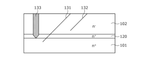
- FIG. 10 is a cross-sectional view showing defect detection in a conventional method for manufacturing a silicon carbide semiconductor device.
- a PL image in the n + type high concentration buffer layer 120 is acquired.
- the PL image of the n + type high concentration buffer layer 120 can be acquired by irradiating excitation light 133 that reaches the inside of the n + type high concentration buffer layer 120.
- the PL image in the n + type high concentration buffer layer 120 can be acquired by setting the wavelength of the excitation light (irradiation light) when acquiring the PL image to 313 nm.
- This PL image can detect defects 131 from the n + type silicon carbide substrate 101 and defects 132 from the n - type silicon carbide epitaxial layer 102.
- the defects 131 from the n + type silicon carbide substrate 101 are killer defects, but the defects 132 from the n - type silicon carbide epitaxial layer 102 are not killer defects.
- the conventional method cannot distinguish between defects 131 from the n + type silicon carbide substrate 101 and defects 132 from the n - type silicon carbide epitaxial layer 102, and also removes chip regions that include only defects 132 from the n - type silicon carbide epitaxial layer 102 as defective chips. This causes a problem of a decrease in the yield rate.
- the present invention aims to provide a silicon carbide semiconductor device and a method for manufacturing a silicon carbide semiconductor device that can remove only chip regions containing defects from a substrate as defective chips in order to solve the problems associated with the conventional techniques described above.
- a silicon carbide semiconductor device has the following features: A vertical silicon carbide semiconductor device having a semiconductor chip formed by epitaxially growing a low-concentration buffer layer and an epitaxial layer having an impurity concentration in the range of 1 ⁇ 10 15 /cm 3 to 1 ⁇ 10 16 /cm 3 on a silicon carbide substrate, the semiconductor chip having electrodes on both main surfaces.
- the low-concentration buffer layer has an impurity concentration higher than that of the epitaxial layer and is 3 ⁇ 10 17 /cm 3 or less, and does not contain defects extending from the silicon carbide substrate to the epitaxial layer.
- the silicon carbide semiconductor device is characterized in that, in the above-mentioned invention, a transition layer is provided between the silicon carbide substrate and the epitaxial layer, the transition layer having an impurity concentration between the impurity concentration of the low-concentration buffer layer and the impurity concentration of the silicon carbide substrate.
- the silicon carbide semiconductor device according to the present invention is also characterized in that, in the above-mentioned invention, the transition layer is thinner than the low-concentration buffer layer.
- the silicon carbide semiconductor device is characterized in that, in the above-mentioned invention, a high-concentration buffer layer having an impurity concentration between the impurity concentration of the transition layer and the impurity concentration of the silicon carbide substrate is provided between the silicon carbide substrate and the epitaxial layer.
- the silicon carbide semiconductor device according to the present invention is characterized in that, in the above-mentioned invention, the high-concentration buffer layer is thicker than the low-concentration buffer layer.
- a silicon carbide semiconductor device has the following features: A vertical silicon carbide semiconductor device is provided with a semiconductor chip on which a low-concentration buffer layer and an epitaxial layer having an impurity concentration in the range of 1 ⁇ 10 15 /cm 3 to 1 ⁇ 10 16 /cm 3 are epitaxially grown on a silicon carbide substrate, the low-concentration buffer layer having an impurity concentration of 3 ⁇ 10 17 /cm 3 or less, and does not contain defects extending from the silicon carbide substrate to the epitaxial layer, but contains defects generated in the epitaxial layer during epitaxial growth.
- the impurity concentration of the low concentration buffer layer is 3 ⁇ 10 17 /cm 3 or less.
- the silicon carbide semiconductor device according to the present invention is characterized in that, in the above-mentioned invention, a transition layer having a higher impurity concentration than the low-concentration buffer layer is provided between the low-concentration buffer layer and the epitaxial layer.
- the method for manufacturing a silicon carbide semiconductor device has the following features.
- This is a method for manufacturing a vertical silicon carbide semiconductor device in which a semiconductor chip in which a low-concentration buffer layer and an epitaxial layer are epitaxially grown on a silicon carbide substrate has electrodes on both main surfaces.
- a pre-process is performed to prepare a semiconductor wafer in which the low-concentration buffer layer and the epitaxial layer are epitaxially grown on the silicon carbide substrate.
- a first detection process is performed to detect defects extending from the silicon carbide substrate to the epitaxial layer and defects generated in the epitaxial layer during the epitaxial growth using a PL image of the low-concentration buffer layer.
- a second detection process is performed to detect defects generated in the epitaxial layer during the epitaxial growth using a PL image of the epitaxial layer.
- a third detection process is performed to detect defects extending from the silicon carbide substrate to the epitaxial layer based on the difference between the detection results of the first detection process and the second detection process.
- a formation process is performed to form a predetermined element structure on the semiconductor wafer.
- a cutting process is performed to dice the semiconductor wafer and separate it into the semiconductor chips.
- a selection process is performed to select the semiconductor chips that do not contain defects extending from the silicon carbide substrate to the epitaxial layer based on the results of the third detection process.
- the method for manufacturing a silicon carbide semiconductor device is characterized in that, in the above-mentioned invention, the first detection step acquires a PL image of the low-concentration buffer layer by positioning the confocal point of the excitation light when acquiring the PL image within the low-concentration buffer layer, and the second detection step acquires a PL image of the epitaxial layer by positioning the confocal point of the excitation light when acquiring the PL image within the epitaxial layer.
- the method for manufacturing a silicon carbide semiconductor device is characterized in that, in the above-mentioned invention, the first detection step acquires a PL image of the low-concentration buffer layer by adjusting the wavelength of the excitation light when acquiring the PL image, and the second detection step acquires a PL image of the epitaxial layer by adjusting the wavelength of the excitation light when acquiring the PL image to be shorter than the wavelength in the first detection step.
- defects inside the low-concentration buffer layer are detected from the difference between the detection results from the PL image of the low-concentration buffer layer and the detection results from the PL image of the epitaxial layer.
- This makes it possible to obtain only the size and position information of the defects from the silicon carbide substrate, which are the killer defects. Therefore, semiconductor chips containing defects from the silicon carbide substrate can be made defective, and semiconductor chips containing only defects from the epitaxial layer can be made good, thereby improving the yield rate.
- the silicon carbide semiconductor device and method of manufacturing the silicon carbide semiconductor device according to the present invention have the advantage that only chip regions containing defects from the substrate can be removed as defective chips.
- FIG. 1 is a plan view showing a layout viewed from the front surface side of a semiconductor wafer on which a silicon carbide semiconductor device according to an embodiment is manufactured (fabricated).
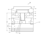
- FIG. 2 is a cross-sectional view showing a structure of a silicon carbide semiconductor device according to an embodiment.
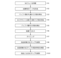
- FIG. 3 is a flowchart showing an outline of a method for manufacturing a silicon carbide semiconductor device according to an embodiment.
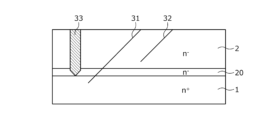
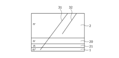
- FIG. 4 is a cross-sectional view showing defect detection from a PL image of n + type buffer layer 20 in the method for manufacturing a silicon carbide semiconductor device according to the embodiment.
- FIG. 1 is a plan view showing a layout viewed from the front surface side of a semiconductor wafer on which a silicon carbide semiconductor device according to an embodiment is manufactured (fabricated).
- FIG. 2 is a cross-sectional view showing a structure of a silicon carbide semiconductor device according to an embodiment.
- FIG. 3 is a flowchart showing an outline of a method for manufacturing a silicon carbide semiconductor device
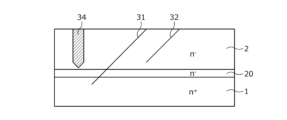
- FIG. 5 is a cross-sectional view showing defect detection from a PL image of an n ⁇ type silicon carbide epitaxial layer in the method for manufacturing a silicon carbide semiconductor device according to the embodiment.
- FIG. 6 is a cross-sectional view showing another structure of the silicon carbide semiconductor device according to the embodiment.
- FIG. 7 is a cross-sectional view showing another structure of the silicon carbide semiconductor device according to the embodiment.
- FIG. 8 is a cross-sectional view showing another structure of the silicon carbide semiconductor device according to the embodiment.
- FIG. 9 is a cross-sectional view showing another structure of the silicon carbide semiconductor device according to the embodiment.
- FIG. 10 is a cross-sectional view showing defect detection in a conventional method for manufacturing a silicon carbide semiconductor device.
- the semiconductor device according to the present invention is configured using a wide band gap semiconductor.
- a trench MOSFET 70 will be described as an example of a silicon carbide semiconductor device fabricated (manufactured) using silicon carbide (SiC) as a wide band gap semiconductor.
- FIG. 1 is a plan view showing the layout, as viewed from the front side, of a semiconductor wafer on which a silicon carbide semiconductor device according to an embodiment is manufactured (created).
- FIG. 2 is a cross-sectional view showing the structure of a silicon carbide semiconductor device according to an embodiment.
- FIG. 2 shows only the active region through which the main current of a trench MOSFET 70 flows.
- the semiconductor wafer 50 may have, for example, an orientation flat (a linear notch provided on part of an edge) 54 or a notch (a V-shaped notch provided on part of an edge: not shown) that indicates the surface orientation.
- Each chip region 51 of the semiconductor wafer 50 is cut (diced) along dicing lines 52 to be singulated into individual semiconductor chips 30.
- All of the semiconductor chips 30 singulated from the same semiconductor wafer 50 have the same silicon carbide semiconductor substrate 18 (see FIG. 2) and the same element structure (here, a trench gate structure: see FIG. 2) formed in the same process.
- the chip regions 51 have a substantially rectangular planar shape, and are arranged in a matrix pattern in the approximate center of the semiconductor wafer 50. Adjacent chip regions 51 are arranged so as to share one side, for example. Dicing lines 52 are formed at the boundaries between adjacent chip regions 51. The dicing lines 52 surround the chip regions 51 in a lattice pattern. The dicing lines 52 are grooves formed in the main surface of the semiconductor wafer 50 (the surface on the silicon carbide semiconductor substrate 18 side in FIG. 2). Within the dicing lines 52, marks (position identification marks: not shown) are formed to identify a position (coordinates) in a direction parallel to the surface of the semiconductor wafer 50.
- the position identification mark is a marker for identifying the position of each chip region 51 and the position of a crystal defect.
- the position identification mark is, for example, a convex or concave portion of a predetermined planar shape (for example, a cross shape) formed by etching within the dicing line 52.
- the position identification mark may be provided in the invalid region 53 of the semiconductor wafer 50.
- the invalid region 53 is a portion between the outermost chip region 51 of the semiconductor wafer 50 and the edge of the semiconductor wafer 50 that is not used as a semiconductor chip 30.
- An alignment mark for aligning each part of the element structure formed in the chip region 51 may be used as the position identification mark.
- the silicon carbide semiconductor device is, for example, an n-channel trench MOSFET 70 having a trench gate structure in an active region on the front surface side of a semiconductor chip 30 made of silicon carbide.
- the active region is a region through which a main current (drift current) flows when the trench MOSFET 70 is in an on-state, and multiple unit cells (functional units of an element) of the trench MOSFET 70 having the same structure are arranged adjacent to each other.
- FIG. 2 shows one unit cell of the trench MOSFET 70.
- the active region is, for example, arranged approximately in the center (chip center) of the semiconductor chip 30, and is surrounded by an edge termination region.
- the edge termination region is the region between the active region and the end (chip end) of the semiconductor chip 30.
- the edge termination region has the function of alleviating the electric field on the front surface side of the semiconductor chip 30 to maintain a breakdown voltage.
- the breakdown voltage is the limit voltage at which the leakage current does not increase excessively and the silicon carbide semiconductor device does not malfunction or break down.
- the silicon carbide semiconductor device is configured using a silicon carbide semiconductor base 18 formed by sequentially stacking an n - type low-concentration buffer layer (buffer layer) 20 , an n - type silicon carbide epitaxial layer (epitaxial layer) 2, and a p-type base layer 6 on a first main surface (front surface), for example a (0001) surface (Si surface), of an n + type silicon carbide substrate (silicon carbide substrate) 1 having an impurity concentration of 5 ⁇ 10 /cm 3 or more.
- the n - type low-concentration buffer layer 20 has an impurity concentration three times or more higher than that of the n - type silicon carbide epitaxial layer 2.
- n-type high concentration region 5 may be provided on the surface of n -type silicon carbide epitaxial layer 2 opposite to n + type silicon carbide substrate 1.
- N-type high concentration region 5 is a high concentration n-type drift layer having an impurity concentration lower than n + type silicon carbide substrate 1 and higher than n -type silicon carbide epitaxial layer 2.
- the impurity concentration of n -type silicon carbide epitaxial layer 2 is within a range of 1 ⁇ 10 15 /cm 3 to 1 ⁇ 10 16 /cm 3 , for example, and the thickness is 10 ⁇ m or more, for example.
- the impurity concentration of the n - type low concentration buffer layer 20 is, for example, 3 ⁇ 10 17 /cm 3 or less, which is in the range of 3 times or more of the impurity concentration of the n - type silicon carbide epitaxial layer 2. If the impurity concentration is higher than 3 ⁇ 10 17 /cm 3 with the excitation light of the PL measurement, triangular polytype stacking faults (hereinafter simply referred to as defects) cannot be detected, so the impurity concentration is set to 3 ⁇ 10 17 /cm 3 or less.
- the thickness of the n - type low concentration buffer layer 20 is preferably, for example, in the range of more than 1 ⁇ m and less than 3 ⁇ m.
- the n-type epitaxial layer 23 includes the n - type silicon carbide epitaxial layer 2 and the n - type low concentration buffer layer 20, and also includes the n-type high concentration region 5 when the n-type high concentration region 5 is provided.
- a back surface electrode 13 serving as a drain electrode is provided on a second main surface (back surface, that is, the back surface of the silicon carbide semiconductor base 18) of the n + type silicon carbide substrate 1.
- a trench structure is formed on the first main surface side (p-type base layer 6 side) of the silicon carbide semiconductor substrate 18. Specifically, the trench 16 penetrates the p-type base layer 6 from the surface of the side opposite to the n + -type silicon carbide substrate 1 side of the p-type base layer 6 (the first main surface side of the silicon carbide semiconductor substrate 18) to the n-type high concentration region 5 (when the n-type high concentration region 5 is not provided, the n - -type silicon carbide epitaxial layer 2, hereinafter simply referred to as (2)).
- a gate insulating film 9 is formed on the bottom and side walls of the trench 16 along the inner wall of the trench 16, and a gate electrode 10 is formed inside the gate insulating film 9 in the trench 16.
- the gate electrode 10 is insulated from the n-type high concentration region 5 (2) and the p-type base layer 6 by the gate insulating film 9. A part of the gate electrode 10 may protrude from the upper side of the trench 16 (the side where the source electrode 12 described later is provided) to the source electrode 12 side.
- a first p + -type base region 3 is provided between the trenches 16 in the surface layer on the opposite side (the first main surface side of the silicon carbide semiconductor base 18) of the n-type high concentration region 5 (2) to the n + -type silicon carbide substrate 1 side.
- a second p + -type base region 4 that contacts the bottom of the trench 16 is provided in the n-type high concentration region 5 (2).
- the second p + -type base region 4 is provided at a position facing the bottom of the trench 16 in the depth direction (the direction from the source electrode 12 to the drain electrode 13).
- the width of the second p + -type base region 4 is the same as or wider than the width of the trench 16.
- the bottom of the trench 16 may reach the second p + -type base region 4, or may be located in the n-type high concentration region 5 (2) sandwiched between the p-type base layer 6 and the second p + -type base region 4.
- n + type region 17 having a peak impurity concentration higher than that of n-type high concentration region 5(2) is provided in n ⁇ type silicon carbide epitaxial layer 2 at a position deeper than first p + type base region 3 between trenches 16. Note that the deeper position refers to a position closer to back surface electrode 13 than first p + type base region 3.
- n + -type source region 7 is selectively provided on the first main surface side of silicon carbide semiconductor substrate 18. Also, p + -type contact region 8 may be selectively provided. Also, n + -type source region 7 and p + -type contact region 8 are in contact with each other.
- the interlayer insulating film 11 is provided on the entire surface of the first main surface side of the silicon carbide semiconductor substrate 18 so as to cover the gate electrode 10 embedded in the trench 16.
- the source electrode 12 contacts the n + type source region 7 and the p type base layer 6 through a contact hole opened in the interlayer insulating film 11.
- the source electrode 12 contacts the n + type source region 7 and the p + type contact region 8.
- the source electrode 12 is electrically insulated from the gate electrode 10 by the interlayer insulating film 11.
- a source electrode pad (not shown) is provided on the source electrode 12.
- a barrier metal 14 made of titanium or titanium nitride that prevents diffusion of metal atoms from the source electrode 12 to the gate electrode 10 may be provided between the source electrode 12 and the interlayer insulating film 11.
- the silicon carbide semiconductor device acquires PL images two or more times to separately detect killer defects, ie, defects 31 extending from the n + type silicon carbide substrate 1 to the n - type silicon carbide epitaxial layer 2 (hereinafter referred to as defects 31 from the n + type silicon carbide substrate 1), and defects 32 generated in the n - type silicon carbide epitaxial layer 2 during epitaxial growth (hereinafter referred to as defects 32 from the n - type silicon carbide epitaxial layer 2), and only the semiconductor chip in which the defect 31 from the n + type silicon carbide substrate 1 exists is made defective.
- defects 31 and 32 see FIG. 4 and FIG. 5.
- the n-type high concentration region 5 there is a defect generated in the n-type high concentration region 5 during epitaxial growth.
- a semiconductor wafer (SiC wafer) 50 using silicon carbide as a semiconductor material is prepared (step S1: pre-process).
- the semiconductor wafer 50 is formed by epitaxially growing an epitaxial layer (corresponding to the n-type epitaxial layer 23 in FIG. 2) on a starting wafer (corresponding to the n + type silicon carbide substrate 1 in FIG. 2) made of silicon carbide.
- a starting wafer made of silicon carbide may be prepared to manufacture the semiconductor wafer 50, or the semiconductor wafer 50 itself may be purchased.
- a position identification mark (not shown) is formed on the main surface (the surface on the n-type epitaxial layer 23 side) of the semiconductor wafer 50 (step S2).
- step S2 position identification marks (not shown) are formed on the main surface of the semiconductor wafer 50 within the dicing lines 52 by photolithography and etching.
- the position identification marks serve as a reference for identifying the positions of crystal defects in the semiconductor wafer 50 (coordinates in a direction parallel to the wafer surface). If the dicing lines 52 are not formed on the semiconductor wafer 50 prepared in the process of step S1, the dicing lines 52 (see FIG. 1) can be formed on the main surface of the semiconductor wafer 50 by photolithography and etching after the process of step S1 and before the process of step S2.
- step S3 first detection step.
- the PL image of the n -type low-concentration buffer layer 20 can be obtained by irradiating it with excitation light 33 that reaches the inside of the n -type low-concentration buffer layer 20, and the size and position information of the defects can be obtained based on the position identification mark.
- step S3 defects from the n -type low-concentration buffer layer 20 to the n -type silicon carbide epitaxial layer 2 are detected using excitation light 33 reaching the inside of the n -type low-concentration buffer layer 20. Therefore, both defects 32 from the n -type silicon carbide epitaxial layer 2 and defects 31 from the n + type silicon carbide substrate 1 are detected.
- step S4 the size (length, surface area, etc.) and position information of defects inside the n -type silicon carbide epitaxial layer 2 are detected from the PL image of the n -type silicon carbide epitaxial layer 2 of the semiconductor wafer 50 taken by the crystal defect inspection device (step S4: second detection step).
- the PL image of the n -type silicon carbide epitaxial layer 2 can be obtained by irradiating the n -type silicon carbide epitaxial layer 2 with excitation light 34 that reaches the inside of the n -type silicon carbide epitaxial layer 2, and the size and position information of the defects can be obtained based on the position specifying mark.
- step S4 defects in the n - type silicon carbide epitaxial layer 2 are detected using excitation light 34 reaching the inside of the n -type silicon carbide epitaxial layer 2. Therefore, defects 32 in the n- type silicon carbide epitaxial layer 2 are detected.
- steps S3 and S4 may be reversed, so that first, the size and position information of defects in n - type silicon carbide epitaxial layer 2 are detected using a PL image of n - type silicon carbide epitaxial layer 2, and then defects from n + type buffer layer 20 to n - type silicon carbide epitaxial layer 2 are detected using a PL image of n + type buffer layer 20.
- PL images are acquired twice, in steps S3 and S4, but PL images may be acquired more than twice. For example, if an epitaxial layer is stacked by multiple epitaxial growths, PL images may be acquired for each epitaxial growth.
- step S5 defects from the n + type silicon carbide substrate 1 and the n - type low concentration buffer layer 20 are detected (step S5: third detection step).
- step S5 a difference is obtained between the size and position information of the defects in the n - type silicon carbide epitaxial layer 2 and the n - type low concentration buffer layer 20 acquired in step S3 and the size and position information of the defects in the n - type silicon carbide epitaxial layer 2 acquired in step S4.
- the size and position information of the defects in the n - type silicon carbide epitaxial layer 2 is deleted, and the size and position information of the defects in the n - type low concentration buffer layer 20 is detected.
- the n -type low-concentration buffer layer 20 is an epitaxial layer, there are also defects from the n -type low-concentration buffer layer 20.
- the n -type low-concentration buffer layer 20 is thinner than the n -type silicon carbide epitaxial layer 2 and the n + type silicon carbide substrate 1, there are few defects from the n -type low-concentration buffer layer 20.
- the defects from the n -type low-concentration buffer layer 20 are treated the same as the defects 31 from the n + type silicon carbide substrate 1. Therefore, only the size and position information of the defects 31 from the n + type silicon carbide substrate 1 is acquired by the process of step S5.
- the PL images in steps S3 and S4 can be acquired as follows.
- the position of the semiconductor layer where defects are detected is changed by adjusting the confocal point without changing the wavelength of the excitation light.
- the position at which the PL image can be acquired is determined by the position of the confocal point of the excitation light.
- the confocal point of the excitation light when acquiring the PL image is set within the n -type low-concentration buffer layer 20, so that the excitation light 33 that reaches the n -type low-concentration buffer layer 20 can be irradiated and the PL image of the n -type low-concentration buffer layer 20 can be acquired.
- step S4 the confocal point of the excitation light when acquiring the PL image is set shallower and within the n -type silicon carbide epitaxial layer 2, so that the excitation light 34 that reaches the inside of the n -type silicon carbide epitaxial layer 2 can be irradiated and the PL image of the n -type silicon carbide epitaxial layer 2 can be acquired.
- the wavelength of the excitation light is changed to change the position of the semiconductor layer where defects are detected.
- the wavelength of the excitation light is increased, a PL image at a deeper position can be acquired. Therefore, in step S3, the wavelength of the excitation light when acquiring the PL image is adjusted to irradiate the excitation light 33 that reaches the n - type low-concentration buffer layer 20, and a PL image of the n - type low-concentration buffer layer 20 can be acquired.
- step S4 the wavelength of the excitation light when acquiring the PL image is adjusted to be shorter to irradiate the excitation light 34 that reaches the inside of the n - type silicon carbide epitaxial layer 2, and a PL image of the n - type silicon carbide epitaxial layer 2 can be acquired.
- defects inside the n - type low-concentration buffer layer 20 are detected by the excitation light 33 with a wavelength of 365 nm
- step S4 defects inside the n - type silicon carbide epitaxial layer 2 are detected by the excitation light 34 with a wavelength of 313 nm.
- Each wavelength varies depending on the impurity concentration and film thickness of n -type low-concentration buffer layer 20 and the impurity concentration and film thickness of n -type silicon carbide epitaxial layer 2.
- the above wavelengths apply when the impurity concentration of n -type low-concentration buffer layer 20 is 3 ⁇ 10 17 /cm 3 or less and is three times or more the impurity concentration of n -type silicon carbide epitaxial layer 2, and the film thickness of n -type silicon carbide epitaxial layer 2 is 70 ⁇ m or less.
- step S6 forming process
- step S8 cutting process
- step S7 cutting process
- step S8 selecting process
- the semiconductor chips 30 that are good candidates are selected based on the information acquired in the processing of step S5 (step S8: selecting process). Specifically, in the processing of step S8, the semiconductor chips 30 that do not include the defects 31 from the n + type silicon carbide substrate 1 are selected as good candidates.
- step S9 inspection process
- various other tests may be performed to confirm or evaluate conditions that do not affect the withstand voltage or reliability. If there is no problem in performing the processing of step S9 or other tests in the state of the semiconductor wafer 50, the processing of step S9 and other tests may be performed after the processing of step S7 and before the processing of step S8.
- the semiconductor chips 30 that are good products are selected based on the results of step S9 (step S10), and the manufacture of the silicon carbide semiconductor device is completed.
- steps S9 and S10 may be omitted, and the semiconductor chip 30 selected in the process of step S8 may be regarded as a non-defective product.
- the n + -type region 17 may be selectively formed in the n -type silicon carbide epitaxial layer 2 by ion implantation, and the n-type epitaxial layer to become the n-type high concentration region 5 may be epitaxially grown, and then the n-type high concentration region 5, the first p + -type base region 3, and the second p + -type base region 4 may be selectively formed in the n-type high concentration region 5 by ion implantation before the p-type epitaxial layer to become the p-type base layer 5 is epitaxially grown.
- a trench MOSFET 70 may have an n-type transition layer 21 between an n - type low-concentration buffer layer 20 and an n - type silicon carbide epitaxial layer 2.
- the n-type transition layer 21 is thinner and has a higher impurity concentration than the n ⁇ -type low-concentration buffer layer 20. Furthermore, the n-type transition layer 21 has a lower impurity concentration than the n + -type silicon carbide substrate 1.
- the film thickness of the n-type transition layer 21 is 0.1 ⁇ m or more and 2 ⁇ m or less, preferably 1 ⁇ m or less, and the impurity concentration of the n-type transition layer 21 is 1 ⁇ 10 18 /cm 3 or more, which is a lower impurity concentration than the n + -type silicon carbide substrate 1.
- the n-type transition layer 21 is a dislocation conversion layer that converts basal plane dislocations (BPDs) into threading edge dislocations (TEDs).
- step S3 the size and position information of defects from the n -type low-concentration buffer layer 20 to the n -type silicon carbide epitaxial layer 2 are detected using the PL image of the n -type low-concentration buffer layer 20, in step S4, the size and position information of defects in the n -type silicon carbide epitaxial layer 2 are detected using the PL image of the n -type silicon carbide epitaxial layer 2, and in step S5, only the size and position information of defects 31 from the n + type silicon carbide substrate 1 is obtained.
- the n - type transition layer 21 is thinner than the n -type silicon carbide epitaxial layer 2 and the n + type silicon carbide substrate 1, and therefore there are few defects originating from the n-type transition layer 21. For this reason, like the defects originating from the n -type low-concentration buffer layer 20, the defects originating from the n-type transition layer 21 are treated the same as the defects 31 originating from the n + type silicon carbide substrate 1.
- Fig. 7 is a partial cross-sectional view of a structure different from the configuration from n + type silicon carbide substrate 1 to n - type silicon carbide epitaxial layer 2 in Fig. 6.
- Fig. 7 differs from Fig. 6 in that an n-type transition layer 21 is formed on n + type silicon carbide substrate 1, an n - type low concentration buffer layer 20 is formed on n type transition layer 21, and an n - type silicon carbide epitaxial layer 2 is formed on n - type low concentration buffer layer 20.
- the impurity concentrations and thicknesses of n + type silicon carbide substrate 1, n type transition layer 21, n - type low concentration buffer layer 20 and n - type silicon carbide epitaxial layer 2 in Fig. 7 may be the same as those in Fig. 6.
- Fig. 8 is a partial cross-sectional view of a structure further different from the configuration from the n + type silicon carbide substrate 1 to the n - type silicon carbide epitaxial layer 2 in Fig. 6 and Fig. 7.
- Fig. 8 differs from Fig. 6 in that an n + type high concentration buffer layer 22 is further formed between the n type transition layer 21 and the n - type silicon carbide epitaxial layer 2.
- the impurity concentrations and thicknesses of the n + type silicon carbide substrate 1, n type transition layer 21, n - type low concentration buffer layer 20 and n - type silicon carbide epitaxial layer 2 in Fig. 8 may be the same as those in Fig. 6.
- the n + type high concentration buffer layer 22 has a function of capturing minority carriers (holes) generated at the interface of the pn junction (pn junctions between the p - type base layer 6 and the first p + type base region 3, and the second p + type base region 4 and the n-type high concentration region 5 and the n - type silicon carbide epitaxial layer 2) that serves as the main junction when a forward current flows, and annihilates them by recombination with majority carriers (electrons), thereby reducing the number of holes that reach the BPDs present on the n + type silicon carbide substrate 1 side of the n + type high concentration buffer layer 22. For this reason, by providing the n + type high concentration buffer layer 22, it is possible to suppress the growth of stacking faults over time due to the use of the SiC-MOSFET.
- n + type high concentration buffer layer 22 is also called a recombination promotion layer, and introduces a lifetime killer into the high doping layer to promote the recombination of holes from n - type silicon carbide epitaxial layer 2, and controls the concentration of holes reaching n + type silicon carbide semiconductor substrate 1, thereby suppressing the occurrence of stacking faults and their area expansion.
- N + type high concentration buffer layer 22 has approximately the same impurity concentration as n + type silicon carbide substrate 1, for example, 3 ⁇ 10 18 /cm 3 or more, and the thickness is preferably 3 ⁇ m to 10 ⁇ m.
- Fig. 9 is a partial cross-sectional view of a structure further different from the configuration from the n + type silicon carbide substrate 1 to the n - type silicon carbide epitaxial layer 2 in Fig. 6, Fig. 7 and Fig. 8.
- Fig. 9 differs from Fig. 8 in that an n type transition layer 21 is formed on the n + type silicon carbide substrate 1, an n - type low concentration buffer layer 20 is formed on the n type transition layer 21, an n + type high concentration buffer layer 22 is formed on the n - type low concentration buffer layer 20, and an n - type silicon carbide epitaxial layer 2 is formed on the n + type high concentration buffer layer 22.
- the impurity concentrations and thicknesses of the n + type silicon carbide substrate 1, the n type transition layer 21, the n - type low concentration buffer layer 20, the n + type high concentration buffer layer 22 and the n - type silicon carbide epitaxial layer 2 in Fig. 9 may be the same as those in Fig. 8.
- the method for manufacturing a silicon carbide semiconductor device described in this embodiment can be realized by executing a previously prepared program on a computer such as a personal computer or a workstation, or on a database server or a web server.
- the size and position information of the crystal defects obtained by this program or the processing of step S3 is recorded on a computer-readable recording medium such as a solid state drive (SSD), a hard disk, a Blu-ray disc (BD: Blu-ray (registered trademark) Disc), a flexible disk, a USB flash memory, a CD-ROM, an MO, or a DVD, and is executed by being read from the recording medium by a computer or a server.
- the program may also be a transmission medium that can be distributed via a network such as the Internet.
- the size and position information of the defect inside the n - type low concentration buffer layer is obtained from the difference between the detection result from the PL image of the n - type low concentration buffer layer and the detection result from the PL image of the n - type silicon carbide epitaxial layer.
- This makes it possible to detect only the size and position information of the defect from the n + type silicon carbide substrate, which is the killer defect. Therefore, it is possible to make the semiconductor chip including the defect from the n + type silicon carbide substrate defective, and to make the semiconductor chip including only the defect from the n - type silicon carbide epitaxial layer good, thereby improving the yield rate.
- each of the above-mentioned embodiments has been described using a trench-gate vertical MOSFET as an example, but it can also be applied to an IGBT (Insulated Gate Bipolar Transistor) or the like.
- each of the embodiments has been described using the first conductivity type as n-type and the second conductivity type as p-type, but the present invention is similarly valid even if the first conductivity type is p-type and the second conductivity type is n-type.
- the silicon carbide semiconductor device and the method for manufacturing the silicon carbide semiconductor device according to the present invention are useful for power semiconductor devices used in power conversion devices such as inverters, power supply devices for various industrial machines, igniters for automobiles, etc.
Landscapes
- Testing Or Measuring Of Semiconductors Or The Like (AREA)
- Recrystallisation Techniques (AREA)
Abstract
Description
本発明にかかる半導体装置は、ワイドバンドギャップ半導体を用いて構成される。実施の形態においては、ワイドバンドギャップ半導体として例えば炭化珪素(SiC)を用いて作製(製造)された炭化珪素半導体装置について、トレンチ型MOSFET70を例に説明する。
次に、実施の形態にかかる炭化珪素半導体装置の製造方法について説明する。図3は、実施の形態にかかる炭化珪素半導体装置の製造方法の概要を示すフローチャートである。
2、102 n-型炭化珪素エピタキシャル層
3 第1p+型ベース領域
4 第2p+型ベース領域
5 n型高濃度領域
6 p型ベース層
7 n+型ソース領域
8 p+型コンタクト領域
9 ゲート絶縁膜
10 ゲート電極
11 層間絶縁膜
12 ソース電極
13 裏面電極
14 バリアメタル
16 トレンチ
17 n+型領域
18 炭化珪素半導体基体
20 n-型低濃度バッファ層
21 n型遷移層
22、120 n+型高濃度バッファ層
23 n型エピタキシャル層
30 半導体チップ
31、131 n+型炭化珪素基板からの欠陥
32、132 n-型エピタキシャル層からの欠陥
33、133 n+型バッファ層に達する励起光
34 エピタキシャル層に達する励起光
50 半導体ウェハ
51 半導体ウェハのチップ領域
52 半導体ウェハのダイシングライン
53 無効領域
54 オリエンテーションフラット
70 トレンチ型MOSFET
Claims (11)
- 炭化珪素基板上に低濃度バッファ層と、不純物濃度が1×10¹⁵/cm3~1×1016/cm3の範囲のエピタキシャル層とをエピタキシャル成長させた半導体チップの両主面にそれぞれ電極を備えた縦型の炭化珪素半導体装置であって、
前記低濃度バッファ層は、前記エピタキシャル層より高不純物濃度でかつ3×10¹⁷/cm3以下の不純物濃度であり、
前記炭化珪素基板から前記エピタキシャル層に延伸した欠陥を含まないことを特徴とする炭化珪素半導体装置。 - 前記炭化珪素基板と前記エピタキシャル層との間に、前記低濃度バッファ層の不純物濃度と前記炭化珪素基板の不純物濃度との間の不純物濃度を有する遷移層を備えることを特徴とする請求項1に記載の炭化珪素半導体装置。
- 前記遷移層は前記低濃度バッファ層より薄いことを特徴とする請求項2に記載の炭化珪素半導体装置。
- 前記炭化珪素基板と前記エピタキシャル層との間に、前記遷移層の不純物濃度と前記炭化珪素基板の不純物濃度との間の不純物濃度を有する高濃度バッファ層を備えることを特徴とする請求項3に記載の炭化珪素半導体装置。
- 前記高濃度バッファ層は前記低濃度バッファ層より厚いことを特徴とする請求項4に記載の炭化珪素半導体装置。
- 炭化珪素基板上に低濃度バッファ層と、不純物濃度が1×10¹⁵/cm3~1×1016/cm3の範囲のエピタキシャル層をエピタキシャル成長させた半導体チップの両主面にそれぞれ電極を備えた縦型の炭化珪素半導体装置であって、
前記低濃度バッファ層は、前記エピタキシャル層より高不純物濃度でかつ3×10¹⁷/cm3以下の不純物濃度であり、
前記炭化珪素基板から前記エピタキシャル層に延伸した欠陥を含まず、
エピタキシャル成長中に前記エピタキシャル層に生成された欠陥を含むことを特徴とする炭化珪素半導体装置。 - 前記低濃度バッファ層の不純物濃度は、3×10¹⁷/cm3以下であることを特徴とする請求項6に記載の炭化珪素半導体装置。
- 前記低濃度バッファ層と前記エピタキシャル層の間に、前記低濃度バッファ層より高不純物濃度である遷移層を備えることを特徴とする請求項6に記載の炭化珪素半導体装置。
- 炭化珪素基板上に低濃度バッファ層とエピタキシャル層をエピタキシャル成長させた半導体チップの両主面にそれぞれ電極を備えた縦型の炭化珪素半導体装置の製造方法であって、
前記炭化珪素基板上に前記低濃度バッファ層と前記エピタキシャル層をエピタキシャル成長させた半導体ウェハを用意する前工程と、
前記低濃度バッファ層のPL像によって、前記炭化珪素基板から前記エピタキシャル層に延伸した欠陥および前記エピタキシャル成長中に前記エピタキシャル層に生成された欠陥を検出する第1検出工程と、
前記エピタキシャル層のPL像によって、前記エピタキシャル成長中に前記エピタキシャル層に生成された欠陥を検出する第2検出工程と、
前記第1検出工程および前記第2検出工程の検出結果の差分より、前記炭化珪素基板から前記エピタキシャル層に延伸した欠陥を検出する第3検出工程と、
前記半導体ウェハに所定の素子構造を形成する形成工程と、
前記形成工程の後、前記半導体ウェハをダイシングして前記半導体チップに個片化する切断工程と、
前記第3検出工程の結果に基づいて、前記炭化珪素基板から前記エピタキシャル層に延伸した欠陥を含まない前記半導体チップを選別する選別工程と、
を含むことを特徴とする炭化珪素半導体装置の製造方法。 - 前記第1検出工程は、PL像を取得の際の励起光の共焦点の位置を前記低濃度バッファ層内にすることで、前記低濃度バッファ層のPL像を取得し、
前記第2検出工程は、PL像を取得の際の励起光の共焦点の位置を前記エピタキシャル層内にすることで、前記エピタキシャル層のPL像を取得することを特徴とする請求項9に記載の炭化珪素半導体装置の製造方法。 - 前記第1検出工程は、PL像を取得の際の励起光の波長を調節することで、前記低濃度バッファ層のPL像を取得し、
前記第2検出工程は、PL像を取得の際の励起光の波長を前記第1検出工程の波長より短く調節することで、前記エピタキシャル層のPL像を取得することを特徴とする請求項9に記載の炭化珪素半導体装置の製造方法。
Priority Applications (4)
| Application Number | Priority Date | Filing Date | Title |
|---|---|---|---|
| JP2024555661A JP7827165B2 (ja) | 2022-10-06 | 2023-08-29 | 炭化珪素半導体装置および炭化珪素半導体装置の製造方法 |
| CN202380029321.1A CN118922947A (zh) | 2022-10-06 | 2023-08-29 | 碳化硅半导体装置及碳化硅半导体装置的制造方法 |
| DE112023000792.6T DE112023000792T5 (de) | 2022-10-06 | 2023-08-29 | Siliziumkarbid-Halbleitervorrichtung und ein Verfahren zum Herstellen einer Siliziumkarbid-Halbleitervorrichtung |
| US18/903,363 US20250022953A1 (en) | 2022-10-06 | 2024-10-01 | Silicon carbide semiconductor device and method of manufacturing silicon carbide semiconductor device |
Applications Claiming Priority (2)
| Application Number | Priority Date | Filing Date | Title |
|---|---|---|---|
| JP2022-161809 | 2022-10-06 | ||
| JP2022161809 | 2022-10-06 |
Related Child Applications (1)
| Application Number | Title | Priority Date | Filing Date |
|---|---|---|---|
| US18/903,363 Continuation US20250022953A1 (en) | 2022-10-06 | 2024-10-01 | Silicon carbide semiconductor device and method of manufacturing silicon carbide semiconductor device |
Publications (1)
| Publication Number | Publication Date |
|---|---|
| WO2024075432A1 true WO2024075432A1 (ja) | 2024-04-11 |
Family
ID=90608004
Family Applications (1)
| Application Number | Title | Priority Date | Filing Date |
|---|---|---|---|
| PCT/JP2023/031087 Ceased WO2024075432A1 (ja) | 2022-10-06 | 2023-08-29 | 炭化珪素半導体装置および炭化珪素半導体装置の製造方法 |
Country Status (5)
| Country | Link |
|---|---|
| US (1) | US20250022953A1 (ja) |
| JP (1) | JP7827165B2 (ja) |
| CN (1) | CN118922947A (ja) |
| DE (1) | DE112023000792T5 (ja) |
| WO (1) | WO2024075432A1 (ja) |
Citations (5)
| Publication number | Priority date | Publication date | Assignee | Title |
|---|---|---|---|---|
| JP2016025241A (ja) * | 2014-07-22 | 2016-02-08 | 住友電気工業株式会社 | 炭化珪素半導体装置の製造方法 |
| WO2017199792A1 (ja) * | 2016-05-20 | 2017-11-23 | 三菱電機株式会社 | 炭化珪素エピタキシャル基板および炭化珪素半導体装置 |
| JP2022016168A (ja) * | 2020-07-10 | 2022-01-21 | 富士電機株式会社 | 半導体装置の製造方法、半導体装置の検査方法および半導体検査装置 |
| JP2022135787A (ja) * | 2021-03-05 | 2022-09-15 | 富士電機株式会社 | 炭化珪素半導体装置および炭化珪素半導体装置の製造方法 |
| WO2022202936A1 (ja) * | 2021-03-24 | 2022-09-29 | 株式会社デンソー | 炭化珪素半導体装置およびそれを用いたインバータ回路、炭化珪素半導体装置の製造方法 |
Family Cites Families (1)
| Publication number | Priority date | Publication date | Assignee | Title |
|---|---|---|---|---|
| JP7175115B2 (ja) | 2018-07-19 | 2022-11-18 | 昭和電工株式会社 | SiCデバイスの製造方法および評価方法 |
-
2023
- 2023-08-29 WO PCT/JP2023/031087 patent/WO2024075432A1/ja not_active Ceased
- 2023-08-29 JP JP2024555661A patent/JP7827165B2/ja active Active
- 2023-08-29 CN CN202380029321.1A patent/CN118922947A/zh active Pending
- 2023-08-29 DE DE112023000792.6T patent/DE112023000792T5/de active Pending
-
2024
- 2024-10-01 US US18/903,363 patent/US20250022953A1/en active Pending
Patent Citations (5)
| Publication number | Priority date | Publication date | Assignee | Title |
|---|---|---|---|---|
| JP2016025241A (ja) * | 2014-07-22 | 2016-02-08 | 住友電気工業株式会社 | 炭化珪素半導体装置の製造方法 |
| WO2017199792A1 (ja) * | 2016-05-20 | 2017-11-23 | 三菱電機株式会社 | 炭化珪素エピタキシャル基板および炭化珪素半導体装置 |
| JP2022016168A (ja) * | 2020-07-10 | 2022-01-21 | 富士電機株式会社 | 半導体装置の製造方法、半導体装置の検査方法および半導体検査装置 |
| JP2022135787A (ja) * | 2021-03-05 | 2022-09-15 | 富士電機株式会社 | 炭化珪素半導体装置および炭化珪素半導体装置の製造方法 |
| WO2022202936A1 (ja) * | 2021-03-24 | 2022-09-29 | 株式会社デンソー | 炭化珪素半導体装置およびそれを用いたインバータ回路、炭化珪素半導体装置の製造方法 |
Also Published As
| Publication number | Publication date |
|---|---|
| US20250022953A1 (en) | 2025-01-16 |
| DE112023000792T5 (de) | 2024-12-19 |
| JPWO2024075432A1 (ja) | 2024-04-11 |
| CN118922947A (zh) | 2024-11-08 |
| JP7827165B2 (ja) | 2026-03-10 |
Similar Documents
| Publication | Publication Date | Title |
|---|---|---|
| US9082845B1 (en) | Super junction field effect transistor | |
| JP5509543B2 (ja) | 半導体装置の製造方法 | |
| US10403554B2 (en) | Method for manufacturing semiconductor device | |
| US12408416B2 (en) | Silicon carbide semiconductor device and method of manufacturing a silicon carbide semiconductor device | |
| US12132084B2 (en) | Silicon carbide semiconductor device and method of manufacturing silicon carbide semiconductor device | |
| US12166120B2 (en) | Silicon carbide semiconductor device and method of manufacturing silicon carbide semiconductor device | |
| US20220367294A1 (en) | Method of manufacturing silicon carbide semiconductor device | |
| CN109390384B (zh) | 碳化硅半导体装置及碳化硅半导体装置的制造方法 | |
| JP7827165B2 (ja) | 炭化珪素半導体装置および炭化珪素半導体装置の製造方法 | |
| JP7537148B2 (ja) | 半導体装置の製造方法、半導体装置の検査方法および半導体検査装置 | |
| JP7669772B2 (ja) | 炭化珪素半導体装置の製造方法 | |
| JP7697262B2 (ja) | 炭化珪素半導体装置の製造方法 | |
| JP6883745B2 (ja) | 半導体装置およびその製造方法 | |
| US9178013B2 (en) | Semiconductor device with edge termination and method for manufacturing a semiconductor device | |
| JP5332376B2 (ja) | 半導体装置とその製造方法 | |
| JP6102171B2 (ja) | 炭化珪素mos型半導体装置の製造方法 | |
| JP7172327B2 (ja) | 炭化珪素半導体装置の製造方法 | |
| JP7601240B2 (ja) | 炭化珪素半導体装置および炭化珪素半導体基板 | |
| US20260101573A1 (en) | Semiconductor device and method of manufacturing semiconductor device | |
| US20250112097A1 (en) | Semiconductor wafer including a test structure | |
| JP2024131769A (ja) | 半導体装置の製造方法 | |
| JP5353036B2 (ja) | 半導体装置の製造方法 |
Legal Events
| Date | Code | Title | Description |
|---|---|---|---|
| 121 | Ep: the epo has been informed by wipo that ep was designated in this application |
Ref document number: 23874564 Country of ref document: EP Kind code of ref document: A1 |
|
| WWE | Wipo information: entry into national phase |
Ref document number: 202380029321.1 Country of ref document: CN |
|
| WWE | Wipo information: entry into national phase |
Ref document number: 112023000792 Country of ref document: DE |
|
| WWE | Wipo information: entry into national phase |
Ref document number: 2024555661 Country of ref document: JP |
|
| 122 | Ep: pct application non-entry in european phase |
Ref document number: 23874564 Country of ref document: EP Kind code of ref document: A1 |