WO2024075428A1 - Condensateur céramique stratifié - Google Patents
Condensateur céramique stratifié Download PDFInfo
- Publication number
- WO2024075428A1 WO2024075428A1 PCT/JP2023/030833 JP2023030833W WO2024075428A1 WO 2024075428 A1 WO2024075428 A1 WO 2024075428A1 JP 2023030833 W JP2023030833 W JP 2023030833W WO 2024075428 A1 WO2024075428 A1 WO 2024075428A1
- Authority
- WO
- WIPO (PCT)
- Prior art keywords
- external electrode
- main surface
- end surface
- ceramic capacitor
- multilayer ceramic
- Prior art date
Links
- 239000003985 ceramic capacitor Substances 0.000 title claims abstract description 99
- 239000000919 ceramic Substances 0.000 claims abstract description 135
- 239000000463 material Substances 0.000 claims description 11
- 239000010409 thin film Substances 0.000 claims description 10
- VNNRSPGTAMTISX-UHFFFAOYSA-N chromium nickel Chemical compound [Cr].[Ni] VNNRSPGTAMTISX-UHFFFAOYSA-N 0.000 claims description 8
- 229910001120 nichrome Inorganic materials 0.000 claims description 8
- 238000005336 cracking Methods 0.000 abstract description 2
- 239000010410 layer Substances 0.000 description 104
- 239000000758 substrate Substances 0.000 description 29
- 238000000034 method Methods 0.000 description 14
- 229910000679 solder Inorganic materials 0.000 description 12
- 238000004519 manufacturing process Methods 0.000 description 8
- 238000007772 electroless plating Methods 0.000 description 6
- 239000003054 catalyst Substances 0.000 description 5
- 229910052751 metal Inorganic materials 0.000 description 5
- 239000002184 metal Substances 0.000 description 5
- 239000011241 protective layer Substances 0.000 description 5
- 239000006071 cream Substances 0.000 description 4
- 230000015572 biosynthetic process Effects 0.000 description 3
- 239000000843 powder Substances 0.000 description 3
- 238000004544 sputter deposition Methods 0.000 description 3
- 239000011230 binding agent Substances 0.000 description 2
- 229910052802 copper Inorganic materials 0.000 description 2
- 238000010586 diagram Methods 0.000 description 2
- 238000004090 dissolution Methods 0.000 description 2
- 230000000694 effects Effects 0.000 description 2
- 229910052737 gold Inorganic materials 0.000 description 2
- 239000011159 matrix material Substances 0.000 description 2
- 150000002739 metals Chemical class 0.000 description 2
- 229910052763 palladium Inorganic materials 0.000 description 2
- 239000011347 resin Substances 0.000 description 2
- 229920005989 resin Polymers 0.000 description 2
- 238000005488 sandblasting Methods 0.000 description 2
- 229910052709 silver Inorganic materials 0.000 description 2
- 239000002002 slurry Substances 0.000 description 2
- 238000005476 soldering Methods 0.000 description 2
- 239000002904 solvent Substances 0.000 description 2
- 229910002367 SrTiO Inorganic materials 0.000 description 1
- 239000003990 capacitor Substances 0.000 description 1
- 239000010408 film Substances 0.000 description 1
- 238000010304 firing Methods 0.000 description 1
- 239000000203 mixture Substances 0.000 description 1
- 238000012986 modification Methods 0.000 description 1
- 230000004048 modification Effects 0.000 description 1
- 229910052759 nickel Inorganic materials 0.000 description 1
Images


Classifications
-
- H—ELECTRICITY
- H01—ELECTRIC ELEMENTS
- H01G—CAPACITORS; CAPACITORS, RECTIFIERS, DETECTORS, SWITCHING DEVICES, LIGHT-SENSITIVE OR TEMPERATURE-SENSITIVE DEVICES OF THE ELECTROLYTIC TYPE
- H01G4/00—Fixed capacitors; Processes of their manufacture
- H01G4/30—Stacked capacitors
Definitions
- the present invention relates to a multilayer ceramic capacitor.
- Multilayer ceramic capacitors are widely used in a variety of devices, including electronic devices and electrical devices (hereinafter referred to as "electronic devices, etc.”).
- electronic devices including electronic devices and electrical devices (hereinafter referred to as "electronic devices, etc.”).
- Patent Document 1 JP 2000-100647 A discloses a multilayer ceramic capacitor with a typical structure.
- circuit boards or circuit board equivalents hereafter both are collectively referred to as "circular boards" using the reflow soldering process described below.
- the substrate on which the capacitor will be mounted is prepared. Electrodes are formed on the main surface of the substrate, and cream solder has already been applied to the surfaces of the electrodes.
- a mounter device equipped with a nozzle is prepared. The top surface (second main surface) of the multilayer ceramic capacitor is then attracted to the nozzle, and the nozzle is then moved to place (place) the bottom surface (first main surface) of the multilayer ceramic capacitor on the pair of electrodes of the substrate on which the cream solder has been applied.
- the substrate on which the multilayer ceramic capacitor is mounted is heated to melt the cream solder, and then the entire substrate is cooled, causing the cream solder to solidify again, and the multilayer ceramic capacitor is mounted to the electrodes of the substrate.
- the present invention aims to provide a multilayer ceramic capacitor that is less likely to cause cracks in the ceramic body even if the ridge line, which is the outer edge of the bottom surface (first main surface) of the ceramic body, collides with the substrate or an electrode formed on the substrate, for example, during mounting.
- a multilayer ceramic capacitor comprises a ceramic body in which a plurality of ceramic layers, a plurality of first internal electrodes, and a plurality of second internal electrodes are stacked in the height direction, the ceramic body having a first main surface and a second main surface opposing each other in the height direction, a first end surface and a second end surface opposing each other in the length direction perpendicular to the height direction, and a first side surface and a second side surface opposing each other in the width direction perpendicular to the height direction and the length direction, and a first external electrode and a second external electrode formed on the outer surface of the ceramic body, the first internal electrode being extended to the first end surface.
- a multilayer ceramic capacitor in which a first external electrode is drawn out to a second end face and electrically connected to the first external electrode, and a second internal electrode is drawn out to a second end face and electrically connected to the second external electrode, and when viewed in a cross section parallel to the first side face and the second side face, the first external electrode is formed in an L-shape on the first end face and the first main face, and the second external electrode is formed in an L-shape on the second end face and the first main face, and the R dimension of the ridge where the first main face meets the first end face, first side face, second end face, and second side face is larger than the R dimension of the ridge where the second main face meets the first end face, first side face, second end face, and second side face.
- the R dimension of the ridges where the first main surface (bottom surface; mounting surface) meets the first end surface, first side surface, second end surface, and second side surface is large, so that even if these ridges collide with the substrate or electrodes formed on the substrate during mounting, cracks are unlikely to occur in the ceramic body.
- FIG. 1 is a perspective view of a multilayer ceramic capacitor 100 according to a first embodiment, showing the multilayer ceramic capacitor 100 from a first main surface 1A side.
- 1 is a perspective view of a multilayer ceramic capacitor 100, showing the multilayer ceramic capacitor 100 from the second main surface 1B side.
- 1A is a cross-sectional view of the multilayer ceramic capacitor 100, showing a cross section of the portion XX indicated by the dashed dotted line arrow in FIG. 1 is a cross-sectional view of a main portion of a multilayer ceramic capacitor 100.
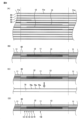
- FIG. 5A to 5D are explanatory views showing steps in an example of a method for manufacturing the multilayer ceramic capacitor 100.
- 6(E) to (J) are continuations of FIG.
- FIG. 4 is a cross-sectional view of a multilayer ceramic capacitor 200 according to a second embodiment.
- 8A to 8D are explanatory diagrams showing steps in an example of a method for manufacturing the multilayer ceramic capacitor 200.
- 9(E) to (J) are continuations of FIG. 8(D), and are explanatory views showing steps in an example of a method for manufacturing the multilayer ceramic capacitor 200.
- each embodiment is an illustrative example of how the present invention can be implemented, and the present invention is not limited to the contents of the embodiment. It is also possible to combine the contents described in different embodiments, and the implementation in such cases is also included in the present invention.
- the drawings are intended to aid in understanding the specification, and may be drawn diagrammatically, and the dimensional ratios of the depicted components or between the components may not match the dimensional ratios of those components described in the specification. Components described in the specification may be omitted in the drawings, or the number of components may be omitted when drawn.
- Figures 1, 2, 3, and 4 each show a multilayer ceramic capacitor 100 according to the first embodiment.
- Figure 1 is a perspective view of the multilayer ceramic capacitor 100, showing the multilayer ceramic capacitor 100 from the first main surface 1A side.
- Figure 2 is also a perspective view of the multilayer ceramic capacitor 100, showing the multilayer ceramic capacitor 100 from the second main surface 1B side.
- Figure 3 is a cross-sectional view of the multilayer ceramic capacitor 100, showing a cross section of the X-X portion indicated by the dashed dotted line arrow in Figure 1(A).
- Figure 4 is a cross-sectional view of a main portion of the multilayer ceramic capacitor 100.
- the drawings show the height direction T, length direction L, and width direction W of the multilayer ceramic capacitor 100, and these directions may be referred to in the following description.
- the stacking direction of the ceramic layers 1a which will be described later, is the height direction T of the multilayer ceramic capacitor 100.
- the multilayer ceramic capacitor 100 includes a ceramic body 1.
- the ceramic body 1 is a rectangular parallelepiped and has a first main surface 1A and a second main surface 1B that face each other in the height direction T, a first end surface 1C and a second end surface 1D that face each other in the length direction L, and a first side surface 1E and a second side surface 1F that face each other in the width direction W.
- the dimensions of the ceramic body 1 are arbitrary, but for example, it is also preferable that one of the dimensions in the length direction L and the width direction W is 1.0 mm or less and the other is 0.5 mm or less. It is also preferable that the dimension in the height direction T is 0.1 mm or less.
- the R dimension of the ridges where the first main surface 1A, which is the mounting surface, meets the first end surface 1C, the first side surface 1E, the second end surface 1D, and the second side surface 1F is large, so that even if the first main surface of the ceramic body collides with the substrate or an electrode formed on the substrate during mounting, the occurrence of cracks in the ceramic body 1 is suppressed.
- the ceramic body 1 is composed of a laminate of a ceramic layer 1a, a first internal electrode 2, a second internal electrode 3, and a dummy internal electrode 4.
- the ceramic layer 1a, the first internal electrode 2, the second internal electrode 3, and the dummy internal electrode 4 are laminated in the height direction T of the ceramic body 1.
- the dummy internal electrode 4 is an electrode that is provided not primarily to form capacitance, but as an underlying external electrode for the first external electrode 5 and the second external electrode 6.
- the ceramic body 1 may be made of any material, and may be, for example, a dielectric ceramic containing BaTiO 3 as a main component. However, instead of BaTiO 3 , a dielectric ceramic containing another material as a main component, such as CaTiO 3 , SrTiO 3 , or CaZrO 3 , may be used.
- the thickness of the ceramic layer 1a is arbitrary, but for example, it can be about 0.3 ⁇ m to 2.0 ⁇ m in the effective capacitance formation area where the first internal electrode 2 and the second internal electrode 3 are formed.
- the number of ceramic layers 1a is arbitrary, but for example, in the effective capacitance formation region where the first internal electrode 2 and the second internal electrode 3 are formed, it can be about 1 to 6000 layers.
- a protective layer (outer layer) is provided that does not have the first internal electrode 2 and the second internal electrode 3 and is composed only of the ceramic layer 1a.
- a dummy internal electrode 4 is formed in the protective layer.
- the thickness of the protective layer is arbitrary, but can be, for example, about 5 ⁇ m to 150 ⁇ m.
- the thickness of the ceramic layer 1a of the protective layer may be greater than the thickness of the ceramic layer 1a in the effective region of capacitance formation where the first internal electrode 2 and the second internal electrode 3 are formed.
- the material of the ceramic layer 1a of the protective layer may be different from the material of the ceramic layer 1a in the effective region.
- the first internal electrode 2 extends in the length direction L of the ceramic body 1, with one end extending to a first end face 1C of the ceramic body 1.
- the second internal electrode 3 extends in the length direction L of the ceramic body 1, with one end extending to a second end face 1D of the ceramic body 1.
- the dummy internal electrode 4 provided as an underlying external electrode for the first external electrode 5 and the second external electrode 6 has a smaller dimension in the length direction L than the first internal electrode 2 and the second internal electrode 3.
- One end of the dummy internal electrode 4 is extended to either the first end face 1C or the second end face 1D of the ceramic body 1.
- the dummy internal electrode 4 disposed closest to the first main surface 1A of the ceramic body 1 is exposed to the first main surface 1A of the ceramic body 1.
- At least the dummy internal electrodes 4 are arranged in the first external electrode 5 and the second external electrode 6 closest to the first main surface 1A of the ceramic body 1, and there should be one layer exposed on the first main surface of the ceramic body 1.
- the main components (metal components) of the first internal electrode 2, second internal electrode 3, and dummy internal electrode 4 may be made of any material, but in this embodiment, Ni is used. However, other metals such as Cu, Ag, Pd, and Au may be used instead of Ni. Furthermore, Ni, Cu, Ag, Pd, and Au may be alloyed with other metals.
- the first internal electrode 2, second internal electrode 3, and dummy internal electrode 4 may contain other components such as ceramics in addition to the metal components.
- the thickness of the first internal electrode 2, the second internal electrode 3, and the dummy internal electrode 4 is arbitrary, but can be, for example, about 0.3 ⁇ m to 1.5 ⁇ m.
- a first external electrode 5 and a second external electrode 6 are formed on the outer surface of the ceramic body 1.
- the first external electrode 5 is formed in an L-shape on the first end surface 1C and the first main surface 1A
- the second external electrode 6 is formed in an L-shape on the second end surface 1D and the first main surface 1A.
- the first external electrode 5 is electrically connected to the first internal electrode 2 at the first end surface 1C.
- the second external electrode 6 is electrically connected to the second internal electrode 3 at the second end surface 1D.
- the first external electrode 5 and the second external electrode 6 have the same multi-layer structure.
- the first external electrode 5 and the second external electrode 6 have, in order from the bottom, a base external electrode, a Cu-plated external electrode layer 7 formed on the outside of the base external electrode, a Ni-plated external electrode layer 8 formed on the outside of the Cu-plated external electrode layer 7, and an Au-plated external electrode layer 9 formed on the outside of the Ni-plated external electrode layer 8.
- the structure and materials of the first external electrode 5 and the second external electrode 6 are arbitrary and are not limited to these structures and materials.
- the dimensions such as thickness, width, and length of the first external electrode 5 and the second external electrode 6 are also arbitrary and can be freely set. In particular, various variations can be adopted for the number of layers, materials, dimensions, etc. of the plated external electrode layers.
- the base external electrode is an electrode that serves as a base when forming a plated external electrode layer on its outside.
- the base external electrode of the first external electrode 5 is composed of the ends of the first internal electrode 2 and dummy internal electrode 4 drawn out to the first end surface 1C, and the main surface of the dummy internal electrode 4 exposed to the first main surface 1A.
- FIG. 3 illustrates a structure in which the first external electrode 5 has four layers of dummy internal electrodes 4 as base external electrodes, the upper main surface of the dummy internal electrode 4 arranged closest to the first main surface 1A is exposed to the first main surface 1A, and the ends of the remaining three layers of dummy internal electrodes 4 are drawn out to the first end surface 1C.
- the number of layers of the dummy internal electrodes 4 of the first external electrode 5 is arbitrary, and it is sufficient that the first external electrode 5 has at least one layer arranged closest to the first main surface 1A of the ceramic body 1 and whose upper main surface is exposed to the outside from the first main surface 1A of the ceramic body 1.
- the base external electrode of the second external electrode 6 is composed of the ends of the second internal electrode 3 and the dummy internal electrode 4 drawn out to the second end surface 1D, and the main surface of the dummy internal electrode 4 exposed to the first main surface 1A.
- the second external electrode 6 has four layers of dummy internal electrodes 4 as base external electrodes, the upper main surface of the dummy internal electrode 4 arranged closest to the first main surface 1A is exposed to the first main surface 1A, and the ends of the remaining three layers of dummy internal electrodes 4 are drawn out to the second end surface 1D.
- the number of layers of the dummy internal electrodes 4 of the second external electrode 6 is arbitrary, and it is sufficient that the second external electrode 6 has at least one layer arranged closest to the first main surface 1A of the ceramic body 1 and whose upper main surface is exposed to the outside from the first main surface 1A of the ceramic body 1.
- the end of the first internal electrode 2 extended to the first end face 1C of the ceramic body 1 and the end of the second internal electrode 3 extended to the second end face 1D of the ceramic body 1 are also part of the underlying external electrodes of the first external electrode 5 and the second external electrode 6.
- the end of the first internal electrode 2 and the end of the second internal electrode 3 are not shown as part of the first external electrode 5 and the second external electrode 6 to avoid complicating the drawings (the leading lines from the reference numeral "5" indicating the first external electrode 5 and the reference numeral "6" indicating the second external electrode 6 have been omitted).
- the base external electrodes of the first external electrode 5 and the second external electrode 6 function as a base for forming a Cu-plated external electrode layer 7 on the outside thereof.
- the end of the first internal electrode 2 extended to the first end face 1C, the end of the dummy internal electrode 4, the end of the second internal electrode 3 extended to the second end face 1D, and the end of the dummy internal electrode 4 are also part of the base external electrodes of the first external electrode 5 and the second external electrode 6.
- the ends of the multiple linear first internal electrodes 2 and the ends of the dummy internal electrodes 4 extending in the width direction W are exposed, and on the second end face 1D, the ends of the multiple linear second internal electrodes 3 and the ends of the dummy internal electrodes 4 extending in the width direction W are exposed at intervals (with the ends of the linear ceramic layers 1a extending in the width direction W sandwiched between them).
- the ends of the first internal electrodes 2, the ends of the second internal electrodes 3, and the ends of the dummy internal electrodes 4 are spaced apart, they function as a base when forming the plated external electrode layer.
- the first external electrode 5 and the second external electrode 6 each have a Cu-plated external electrode layer 7 on the outside of the base external electrode.
- the Cu-plated external electrode layer 7 mainly functions to improve moisture resistance. It is also preferable that the Cu-plated external electrode layer 7 contains Ni. In this case, dissolution of the external electrode layer into the solder can be suppressed.
- the first external electrode 5 and the second external electrode 6 each have a Ni-plated external electrode layer 8 on the outside of the Cu-plated external electrode layer 7.
- the Ni-plated external electrode layer 8 mainly functions to improve solder heat resistance and bondability. It is also preferable that the Ni-plated external electrode layer 8 contains P. In this case, the mechanical strength of the external electrode layer can be improved.
- the first external electrode 5 and the second external electrode 6 have an Au-plated external electrode layer 9 on the outside of the Ni-plated external electrode layer 8.
- the Au-plated external electrode layer 9 mainly serves the function of improving the wettability of the external electrode layer to the solder.
- the R dimensions of the ridgeline E11 where the first main surface 1A and the first end surface 1C meet, the ridgeline E12 where the first main surface 1A and the first side surface 1E meet, the ridgeline E13 where the first main surface 1A and the second end surface 1D meet, and the ridgeline E14 where the first main surface 1A and the second side surface 1F meet are larger than the R dimensions of the ridgeline E21 where the second main surface 1B and the first end surface 1C meet, the ridgeline E22 where the second main surface 1B and the first side surface 1E meet, the ridgeline E23 where the second main surface 1B and the second end surface 1D meet, and the ridgeline E24 where the second main surface 1B and the second side surface 1F meet.
- the manufacturing process includes a separate step of increasing the R dimension for ridgeline E11 where first main surface 1A meets first end surface 1C, ridgeline E12 where first main surface 1A meets first side surface 1E, ridgeline E13 where first main surface 1A meets second end surface 1D, and ridgeline E14 where first main surface 1A meets second side surface 1F.
- the manufacturing process does not include a step of increasing the R dimension for ridgeline E21 where second main surface 1B meets first end surface 1C, ridgeline E22 where second main surface 1B meets first side surface 1E, ridgeline E23 where second main surface 1B meets second end surface 1D, and ridgeline E24 where second main surface 1B meets second side surface 1F.
- the first main surface 1A of the ceramic body 1, which is provided with the first external electrode 5 and the second external electrode 6, is the mounting surface for the substrate (as described above, “substrate” includes “substrate-like objects”).
- the multilayer ceramic capacitor 100 has a large R dimension (large roundness) for the ridgeline E11 where the first main surface 1A and the first end surface 1C meet, the ridgeline E12 where the first main surface 1A and the first side surface 1E meet, the ridgeline E13 where the first main surface 1A and the second end surface 1D meet, and the ridgeline E14 where the first main surface 1A and the second side surface 1F meet, which are provided on the mounting surface side.
- the multilayer ceramic capacitor 100 is placed (placed) on a substrate for mounting, even if these ridgelines collide with the substrate or electrodes formed on the substrate, the impact is mitigated, and the occurrence of cracks in the ceramic body 1 is suppressed.
- each of the R dimensions of the ridgeline E11 where the first main surface 1A and the first end surface 1C meet, the ridgeline E12 where the first main surface 1A and the first side surface 1E meet, the ridgeline E13 where the first main surface 1A and the second end surface 1D meet, and the ridgeline E14 where the first main surface 1A and the second side surface 1F meet is, for example, about 1 ⁇ m or more and 10 ⁇ m or less. This is because if it is less than 1 ⁇ m, the effect of suppressing the occurrence of cracks and the like in the ceramic body 1 is small.
- the process of increasing the R dimensions of each of these ridgelines takes time, reducing the productivity of the multilayer ceramic capacitor.
- the R dimensions of the ridgeline E21 where the second main surface 1B and the first end surface 1C meet, the ridgeline E22 where the second main surface 1B and the first side surface 1E meet, the ridgeline E23 where the second main surface 1B and the second end surface 1D meet, and the ridgeline E24 where the second main surface 1B and the second side surface 1F meet are each less than about 1 ⁇ m, for example. In this case, there is no need to provide a separate process for increasing the R dimensions of these ridgelines.
- the multilayer ceramic capacitor 100 of this embodiment has a corner C11 where the first main surface 1A, the first end surface 1C, and the first side surface 1E meet, a corner C12 where the first main surface 1A, the first side surface 1E, and the second end surface 1D meet, a corner C13 where the first main surface 1A, the second end surface 1D, and the second side surface 1F meet, a corner C14 where the first main surface 1A, the second side surface 1F, and the first end surface 1C meet, and a corner C15 where the first main surface 1A, the second end surface 1D, and the second side surface 1F meet.
- the R dimension of corner C14 where surface 1C meets is larger than the R dimensions of corner C21 where second main surface 1B, first end surface 1C and first side surface 1E meet, corner C22 where second main surface 1B, first side surface 1E and second end surface 1D meet, corner C23 where second main surface 1B, second end surface 1D and second side surface 1F meet, and corner C24 where second main surface 1B, second side surface 1F and first end surface 1C meet.
- the R dimensions of the ridgeline E11 where the first main surface 1A and the first end surface 1C meet, the ridgeline E12 where the first main surface 1A and the first side surface 1E meet, the ridgeline E13 where the first main surface 1A and the second end surface 1D meet, and the ridgeline E14 where the first main surface 1A and the second side surface 1F meet are larger than the R dimensions of the ridgeline E21 where the second main surface 1B and the first end surface 1C meet, the ridgeline E22 where the second main surface 1B and the first side surface 1E meet, the ridgeline E23 where the second main surface 1B and the second end surface 1D meet, and the ridgeline E24 where the second main surface 1B and the second side surface 1F meet.
- the R dimension of the corner where two ridgelines with a large R dimension intersect is larger than the R dimension of the corner where two ridgelines with a small R dimension intersect.
- the laminated ceramic capacitor 100 has corners C11 on the mounting surface where the first main surface 1A, first end surface 1C, and first side surface 1E meet, corner C12 where the first main surface 1A, first side surface 1E, and second end surface 1D meet, corner C13 where the first main surface 1A, second end surface 1D, and second side surface 1F meet, and corner C14 where the first main surface 1A, second side surface 1F, and first end surface 1C meet.
- the multilayer ceramic capacitor 100 of this embodiment has a plurality of embossed holes 10 formed on the second main surface 1B of the ceramic body 1.
- a plurality of embossed holes 10 of the same shape and dimensions are formed on the second main surface 1B of the ceramic body 1 in a state aligned in the length direction L and width direction W.
- an embossed hole refers to a bottomed hole with a concave surface.
- the concave surface may be hemispherical or non-hemispherical.
- the method of forming the embossed holes 10 is also arbitrary. Whether or not embossed holes 10 are formed in the second main surface 1B can be easily confirmed by comparing with other surfaces of the ceramic body 1 (such as the first main surface 1A).
- the second main surface 1B of the ceramic body 1 is the surface that is sucked by, for example, the nozzle of a mounter device during mounting, and is the surface that may be subjected to impact by the nozzle.
- the multilayer ceramic capacitor 100 of this embodiment since a plurality of embossed holes 10 are formed in the second main surface 1B of the ceramic body 1, even if an impact is applied by a nozzle or the like, the multilayer ceramic capacitor 100 is resistant to the impact, and the occurrence of cracks in the ceramic body 1 is suppressed. Note that if the embossed holes 10 are minute and the depth is contained within one to several tens of ceramic layers 1a, the impact resistance of the ceramic body 1 can be improved satisfactorily. However, if the depth of the embossed holes 10 is too large, it may conversely reduce the overall strength of the ceramic body 1, so it is necessary that the depth of the embossed holes 10 is not too large.
- the multilayer ceramic capacitor 100 of this embodiment can be manufactured, for example, by the method shown in Figures 5(A) to 6(J).
- a ceramic green sheet 11a is prepared for producing the ceramic layer 1a of the ceramic body 1, as shown in FIG. 5(A).
- the ceramic green sheet 11a is prepared as a mother ceramic green sheet 50 in which a large number of ceramic green sheets 11a are arranged in a matrix in order to manufacture a large number of multilayer ceramic capacitors 100 at once.
- dielectric ceramic powder, binder resin, solvent, etc. are prepared and then wet-mixed to create ceramic slurry.
- the ceramic slurry is applied in sheet form onto the carrier film using a die coater, gravure coater, microgravure coater, etc., and dried to produce the mother ceramic green sheet 50.
- a conductive paste 12 for forming the first internal electrode 2, a conductive paste 13 for forming the second internal electrode 3, and a conductive paste 14 for forming the dummy internal electrode 4, which have been prepared in advance, are applied (e.g., printed) in a desired pattern shape to the main surface of a predetermined ceramic green sheet 11a in the mother ceramic green sheet 50.
- the conductive paste may be, for example, a mixture of a solvent, a binder resin, a metal powder (e.g., Ni powder), etc.
- the mother ceramic green sheets 50 are stacked in a predetermined order and pressed together to produce a mother unsintered ceramic body 60 in which numerous unsintered ceramic bodies 11 are arranged in a matrix.
- a jig 70 is prepared with multiple protrusions 70a formed on its upper main surface.
- the lower main surface of the mother unsintered ceramic body 60 is then pressed against the protrusions 70a of the jig 70.
- multiple embossed holes 10 are formed in the second main surface 1B of each unsintered ceramic body 11 of the mother unsintered ceramic body 60.
- the mother unsintered ceramic body 60 is cut into individual unsintered ceramic bodies 11.
- the unsintered ceramic body 11 is fired with a predetermined profile to produce the ceramic body 1 shown in FIG. 6(F).
- a conductive paste 12 is fired at the same time to form a first internal electrode 2
- a conductive paste 13 is fired at the same time to form a second internal electrode 3
- a conductive paste 14 is fired at the same time to form a dummy internal electrode 4.
- a jig 80 is prepared.
- the second main surface 1B of the ceramic body 1 is fixed to the upper main surface of the jig 80.
- the first main surface 1A of the ceramic body 1 is scraped off, for example by sandblasting, so that the upper main surface of the dummy internal electrode 4 that is disposed closest to the first main surface 1A of the ceramic body 1 is exposed to the first main surface 1A of the ceramic body 1.
- the ridgeline E11 where the first main surface 1A and the first end surface 1C meet, the ridgeline E12 where the first main surface 1A and the first side surface 1E meet, the ridgeline E13 where the first main surface 1A and the second end surface 1D meet, and the ridgeline E14 where the first main surface 1A and the second side surface 1F meet are each cut away, and the ridgeline E11 where the first main surface 1A and the first end surface 1C meet, the ridgeline E12 where the first main surface 1A and the first side surface 1E meet, and the ridgeline E14 where the first main surface 1A and the first
- the R dimensions of the ridgeline E13 where the first main surface 1A and the second end surface 1D meet, and the ridgeline E14 where the first main surface 1A and the second side surface 1F meet are larger (more rounded) than the R dimensions of the ridgeline E21 where the second main surface 1B and the first end surface 1C meet, the ridgeline E22 where the second main surface 1
- the ends of the first internal electrode 2, the second internal electrode 3, and the dummy internal electrode 4 extended to the first end face 1C and the second end face 1D, and the upper main surface of the dummy internal electrode 4 exposed to the first main surface 1A are used as base external electrodes, and a predetermined catalyst is applied to the surfaces of these base external electrodes as necessary, followed by electroless plating to form a Cu-plated external electrode layer 7.
- a specific catalyst is applied to the outside of the Cu-plated external electrode layer 7 as necessary, and then electroless plating is performed to form the Ni-plated external electrode layer 8.
- the first external electrode 5 is formed in an L-shape on the first end face 1C and first main face 1A of the ceramic body 1
- the second external electrode 6 is formed in an L-shape on the second end face 1D and first main face 1A of the ceramic body 1, completing the multilayer ceramic capacitor 100 according to the first embodiment.
- FIG. 7 shows a multilayer ceramic capacitor 200 according to the second embodiment. Note that FIG. 7 is a cross-sectional view of the multilayer ceramic capacitor 200.
- the multilayer ceramic capacitor 200 according to the second embodiment is a modified version of the multilayer ceramic capacitor 100 according to the first embodiment described above.
- a dummy internal electrode 4 was used as part of the underlying external electrodes for the first external electrode 5 and the second external electrode 6.
- the multilayer ceramic capacitor 200 changes this by omitting the dummy internal electrode 4.
- a NiCr thin film layer 27 is formed by sputtering as the underlying external electrode for the first external electrode 25 and the second external electrode 26.
- the NiCr thin film layer 27 has high adhesion to the ceramic body 1, and serves as an excellent underlying external electrode for the first external electrode 25 and the second external electrode 26.
- the plated external electrode layers of the first external electrode 5 and the second external electrode 6 were provided in the order of Cu-plated external electrode layer 7, Ni-plated external electrode layer 8, and Au-plated external electrode layer 9 on the outside of the base external electrode.
- the other configurations of the multilayer ceramic capacitor 200 are the same as those of the multilayer ceramic capacitor 100.
- the R dimensions of the ridgeline E11 where the first main surface 1A and the first end surface 1C meet, the ridgeline E12 where the first main surface 1A and the first side surface 1E meet, the ridgeline E13 where the first main surface 1A and the second end surface 1D meet, and the ridgeline E14 where the first main surface 1A and the second side surface 1F meet are larger than the R dimensions of the ridgeline E21 where the second main surface 1B and the first end surface 1C meet, the ridgeline E22 where the second main surface 1B and the first side surface 1E meet, the ridgeline E23 where the second main surface 1B and the second end surface 1D meet, and the ridgeline E24 where the second main surface 1B and the second side surface 1F meet. Therefore, even if these ridges collide with the substrate or electrodes formed on the substrate when the multilayer ceramic capacitor 200 is placed on a substrate for mounting, the impact is mitigated, preventing cracks from occurring in the
- the multilayer ceramic capacitor 200 of this embodiment can be manufactured, for example, by the method shown in Figures 8(A) to 9(J).
- a ceramic green sheet 11a is prepared for producing the ceramic layer 1a of the ceramic body 1, as shown in FIG. 8(A).
- the ceramic green sheet 11a is prepared as a mother ceramic green sheet 50 for manufacturing a large number of multilayer ceramic capacitors 100 at once.
- a conductive paste 12 for forming the first internal electrode 2 and a conductive paste 13 for forming the second internal electrode 3, which have been prepared in advance, are applied in a desired pattern shape to the main surface of a predetermined ceramic green sheet 11a in the mother ceramic green sheet 50. Note that since the multilayer ceramic capacitor 200 does not have a dummy internal electrode, no conductive paste for forming a dummy internal electrode is applied.
- the mother ceramic green sheets 50 are stacked in a predetermined order and pressed together to produce the mother unsintered ceramic body 60.
- the lower main surface of the mother unsintered ceramic body 60 is pressed against a jig 70 having multiple protrusions 70a formed on its upper main surface, and as shown in FIG. 8(D), multiple embossed holes 10 are formed in the second main surface 1B of each unsintered ceramic body 11.
- the mother unsintered ceramic body 60 is cut into individual unsintered ceramic bodies 11.
- the unsintered ceramic body 11 is fired with a predetermined profile to produce the ceramic body 1 shown in Figure 9 (F).
- a jig 80 is prepared.
- the second main surface 1B of the ceramic body 1 is fixed to the upper main surface of the jig 80.
- sandblasting is performed to remove the ridgeline E11 where the first main surface 1A and the first end surface 1C meet, the ridgeline E12 where the first main surface 1A and the first side surface 1E meet, the ridgeline E13 where the first main surface 1A and the second end surface 1D meet, and the ridgeline E14 where the first main surface 1A and the second side surface 1F meet, thereby increasing their R dimensions.
- a NiCr thin film layer 27 is formed by sputtering as an underlying external electrode for the first external electrode 25 and the second external electrode 26.
- a specified catalyst is applied to the outside of the NiCr thin film layer 27, which is the base external electrode of the first external electrode 25 and the second external electrode 26, if necessary, and then electroless plating is performed to form the Ni-plated external electrode layer 28.
- a predetermined catalyst is applied to the outside of the Ni-plated external electrode layer 28 if necessary, and then electroless plating is performed to form an Au-plated external electrode layer 29.
- an L-shaped first external electrode 25 is formed on the first end face 1C and first main surface 1A of the ceramic body 1
- an L-shaped second external electrode 26 is formed on the second end face 1D and first main surface 1A of the ceramic body 1, completing the multilayer ceramic capacitor 200 according to the second embodiment.
- a process was provided for increasing the R dimensions of ridgeline E11 where the first main surface 1A and the first end surface 1C meet, ridgeline E12 where the first main surface 1A and the first side surface 1E meet, ridgeline E13 where the first main surface 1A and the second end surface 1D meet, and ridgeline E14 where the first main surface 1A and the second side surface 1F meet, but a process was not provided for increasing the R dimensions of ridgeline E21 where the second main surface 1B and the first end surface 1C meet, ridgeline E22 where the second main surface 1B and the first side surface 1E meet, ridgeline E23 where the second main surface 1B and the second end surface 1D meet, and ridgeline E24 where the second main surface 1B and the second side surface 1F meet.
- the R dimensions of the ridgeline E12 where the surface 1A meets the first side surface 1E, the ridgeline E13 where the first main surface 1A meets the second end surface 1D, and the ridgeline E14 where the first main surface 1A meets the second side surface 1F may be larger than the R dimensions of the ridgeline E21 where the second main surface 1B meets the first end surface 1C, the ridgeline E22 where the second main surface 1B meets the first side surface 1E, the ridgeline E23 where the second main surface 1B meets the second end surface 1D, and the ridgeline E24 where the second main surface 1B meets the second side surface 1F.
- the embossed holes 10 are formed in the second main surface 1B of the ceramic body 1, but in the multilayer ceramic capacitor of the present invention, the embossed holes 10 are not an essential component and can be omitted.
- the multilayer ceramic capacitor according to one embodiment of the present invention is as described in the "Means for solving the problems" section.
- the R dimension of the ridges where the first main surface meets the first end face, the second end face, the first side face, and the second side face is 1 ⁇ m or more and 10 ⁇ m or less. If it is less than 1 ⁇ m, the effect of suppressing the occurrence of cracks in the ceramic body when these ridges collide with a substrate or the like is small. Also, if it exceeds 10 ⁇ m, the process of increasing the R dimension of each of these ridges takes time, reducing the productivity of the multilayer ceramic capacitor.
- the R dimension of the corner where the first main surface, the first end face and the first side surface meet, the corner where the first main surface, the first side surface and the second end face meet, the corner where the first main surface, the second end face and the second side surface meet, and the corner where the first main surface, the second side surface and the first end face meet is larger than the R dimension of the corner where the second main surface, the first end face and the first side surface meet, the corner where the second main surface, the first side surface and the second end face meet, the corner where the second main surface, the second end face and the second side surface meet, and the corner where the second main surface, the second side surface and the first end face meet.
- the corners on the mounting surface where the first main surface, the first end surface, and the first side surface meet, the corners where the first main surface, the first side surface, and the second end surface meet, the corners where the first main surface, the second end surface, and the second side surface meet, and the corners where the first main surface, the second side surface, and the first end surface meet have large R dimensions. Therefore, even if these corners collide with the substrate or an electrode formed on the substrate when the multilayer ceramic capacitor is placed on a substrate or the like for mounting, the impact is mitigated, and the occurrence of cracks in the ceramic body is suppressed.
- a plurality of embossed holes are formed on the second main surface of the ceramic body.
- the ceramic body is resistant to the impact and the occurrence of cracks or the like in the ceramic body is suppressed.
- the first external electrode and the second external electrode each include a base external electrode and at least one plated external electrode layer formed on the outside of the base external electrode.
- the plated external electrode layer can be easily formed on the outside of the base external electrode by, for example, electroless plating.
- the base external electrode includes a dummy internal electrode that is smaller in length than the first internal electrode and the second internal electrode and is exposed on the first main surface of the ceramic body. In this case, it is possible to easily form the first external electrode and the second external electrode that have a relatively large area on the first main surface of the ceramic body.
- the dummy internal electrode, the first internal electrode, and the second external electrode are formed from the same material. In this case, there is no need to prepare a separate material to form the dummy internal electrode, which is the base external electrode, improving the productivity of the multilayer ceramic capacitor.
- the dummy internal electrode is mainly composed of Ni.
- the ceramic body, the first internal electrode, the second external electrode, and the dummy internal electrode can be easily produced by so-called simultaneous firing.
- the base external electrode is a thin film.
- the base external electrode can be easily formed, for example, by sputtering.
- the thin film is mainly composed of NiCr. In this case, it has high adhesion to the ceramic body and serves as an excellent base external electrode for the first and second external electrodes.
- the plated external electrode layer includes at least one selected from a Cu-plated external electrode layer, a Ni-plated external electrode layer, and an Au-plated external electrode layer.
- various functions are exerted in each plated external electrode layer, and excellent first and second external electrodes can be formed.
- the plated external electrode layer includes a Ni-plated external electrode layer formed on the outside of the base external electrode, and an Au-plated external electrode layer formed on the outside of the Ni-plated external electrode layer.
- the Ni-plated external electrode layer can mainly function to improve the solder heat resistance and bondability
- the Au-plated external electrode layer 9 can mainly function to improve the wettability of the external electrode layer to the solder.
- the plated external electrode layer includes a Cu-plated external electrode layer formed on the outside of the base external electrode, a Ni-plated external electrode layer formed on the outside of the Cu-plated external electrode layer, and an Au-plated external electrode layer formed on the outside of the Ni-plated external electrode layer.
- the Cu-plated external electrode layer 7 can mainly function to improve moisture resistance
- the Ni-plated external electrode layer can mainly function to improve solder heat resistance and bondability
- the Au-plated external electrode layer 9 can mainly function to improve the wettability of the external electrode layer to solder.
- the Ni-plated external electrode layer contains P. In this case, the mechanical strength of the external electrode layer is improved.
- the Cu-plated external electrode layer contains Ni. In this case, dissolution of the external electrode layer into the solder can be suppressed.
- one of the lengthwise dimension and widthwise dimension is 1.0 mm or less, and the other is 0.5 mm or less. It is also preferable that the heightwise dimension is 0.1 mm or less. Even when the present invention is applied to a multilayer ceramic capacitor that is miniaturized and thinned in this way, the R dimension of the ridges where the first main surface, which is the mounting surface, meets the first end face, first side face, second end face, and second side face is large, so that even if these ridges collide with the substrate or electrodes formed on the substrate during mounting, the occurrence of cracks in the ceramic body is suppressed.
- Ceramic body 1a Ceramic layer 1A: First main surface 1B: Second main surface 1C: First end surface 1D: Second end surface 1E: First side surface 1F: Second side surface 2: First internal electrode 3: Second internal electrode 4: Dummy internal electrode 5: First external electrode 6: Second external electrode 7: Cu-plated external electrode layer 8, 28: Ni-plated external electrode layer 9, 29: Au-plated external electrode layer 27: NiCr thin film layer (base external electrode) 10: Embossed hole
Landscapes
- Engineering & Computer Science (AREA)
- Power Engineering (AREA)
- Manufacturing & Machinery (AREA)
- Microelectronics & Electronic Packaging (AREA)
- Fixed Capacitors And Capacitor Manufacturing Machines (AREA)
- Ceramic Capacitors (AREA)
Abstract
L'invention concerne un condensateur céramique stratifié grâce auquel la fissuration ou similaire est moins susceptible de se produire dans un corps en céramique. L'invention concerne un condensateur céramique stratifié comprenant : un corps en céramique, dans lequel une pluralité de couches de céramique, une pluralité de premières électrodes internes et une pluralité de secondes électrodes internes sont stratifiées dans la direction de la hauteur, et qui possède une première surface principale et une seconde surface principale qui se font face dans la direction de la hauteur, une première surface d'extrémité et une seconde surface d'extrémité qui se font face dans la direction de la longueur orthogonale à la direction de la hauteur, et une première surface latérale et une seconde surface latérale qui se font face dans la direction de la largeur orthogonale à la direction de la hauteur et à la direction de la longueur ; et une première électrode externe et une seconde électrode externe qui sont formées sur une surface externe du corps en céramique. Les premières électrodes internes sont tirées vers la première surface d'extrémité et connectées électriquement à la première électrode externe ; et les secondes électrodes internes sont tirées vers la seconde surface d'extrémité et connectées électriquement à la seconde électrode externe. Lorsqu'une section transversale parallèle à la première surface latérale et à la seconde surface latérale est vue, la première électrode externe est formée en forme de L sur la première surface d'extrémité et la première surface principale, et la seconde électrode externe est formée en forme de L sur la seconde surface d'extrémité et la première surface principale ; et une dimension R d'une ligne de crête où la première surface principale et la première surface d'extrémité, la première surface latérale, la seconde surface d'extrémité et la seconde surface latérale sont en contact est supérieure à une dimension R d'une ligne de crête où la seconde surface principale et la première surface d'extrémité, la première surface latérale, la seconde surface d'extrémité et la seconde surface latérale sont en contact.
Applications Claiming Priority (2)
| Application Number | Priority Date | Filing Date | Title |
|---|---|---|---|
| JP2022-160614 | 2022-10-04 | ||
| JP2022160614 | 2022-10-04 |
Publications (1)
| Publication Number | Publication Date |
|---|---|
| WO2024075428A1 true WO2024075428A1 (fr) | 2024-04-11 |
Family
ID=90607992
Family Applications (1)
| Application Number | Title | Priority Date | Filing Date |
|---|---|---|---|
| PCT/JP2023/030833 WO2024075428A1 (fr) | 2022-10-04 | 2023-08-27 | Condensateur céramique stratifié |
Country Status (1)
| Country | Link |
|---|---|
| WO (1) | WO2024075428A1 (fr) |
Citations (12)
| Publication number | Priority date | Publication date | Assignee | Title |
|---|---|---|---|---|
| JPH0270402U (fr) * | 1988-11-17 | 1990-05-29 | ||
| JP2004153098A (ja) * | 2002-10-31 | 2004-05-27 | Nec Tokin Corp | 積層セラミックコンデンサおよびその製造方法 |
| JP2012043841A (ja) * | 2010-08-13 | 2012-03-01 | Murata Mfg Co Ltd | 積層型セラミック電子部品およびその製造方法 |
| JP2012164966A (ja) * | 2011-01-21 | 2012-08-30 | Murata Mfg Co Ltd | セラミック電子部品 |
| JP2016072279A (ja) * | 2014-09-26 | 2016-05-09 | 株式会社村田製作所 | 積層セラミックコンデンサ、これを含む積層セラミックコンデンサ連、および、積層セラミックコンデンサの実装体 |
| CN205248112U (zh) * | 2015-12-04 | 2016-05-18 | 东莞市平尚电子科技有限公司 | 贴片高压电容 |
| JP2019062100A (ja) * | 2017-09-27 | 2019-04-18 | 太陽誘電株式会社 | セラミック電子部品およびその製造方法 |
| JP2020167231A (ja) * | 2019-03-28 | 2020-10-08 | 株式会社村田製作所 | 積層セラミックコンデンサおよび積層セラミックコンデンサの製造方法 |
| JP2021120977A (ja) * | 2020-01-30 | 2021-08-19 | 株式会社村田製作所 | 積層セラミック電子部品及び積層セラミック電子部品の実装構造 |
| JP2022085195A (ja) * | 2020-11-27 | 2022-06-08 | 太陽誘電株式会社 | セラミック電子部品、実装基板およびセラミック電子部品の製造方法 |
| JP2022090195A (ja) * | 2020-12-07 | 2022-06-17 | 太陽誘電株式会社 | セラミック電子部品、実装基板およびセラミック電子部品の製造方法 |
| JP2022142240A (ja) * | 2021-03-16 | 2022-09-30 | 株式会社村田製作所 | 積層セラミックコンデンサ |
-
2023
- 2023-08-27 WO PCT/JP2023/030833 patent/WO2024075428A1/fr unknown
Patent Citations (12)
| Publication number | Priority date | Publication date | Assignee | Title |
|---|---|---|---|---|
| JPH0270402U (fr) * | 1988-11-17 | 1990-05-29 | ||
| JP2004153098A (ja) * | 2002-10-31 | 2004-05-27 | Nec Tokin Corp | 積層セラミックコンデンサおよびその製造方法 |
| JP2012043841A (ja) * | 2010-08-13 | 2012-03-01 | Murata Mfg Co Ltd | 積層型セラミック電子部品およびその製造方法 |
| JP2012164966A (ja) * | 2011-01-21 | 2012-08-30 | Murata Mfg Co Ltd | セラミック電子部品 |
| JP2016072279A (ja) * | 2014-09-26 | 2016-05-09 | 株式会社村田製作所 | 積層セラミックコンデンサ、これを含む積層セラミックコンデンサ連、および、積層セラミックコンデンサの実装体 |
| CN205248112U (zh) * | 2015-12-04 | 2016-05-18 | 东莞市平尚电子科技有限公司 | 贴片高压电容 |
| JP2019062100A (ja) * | 2017-09-27 | 2019-04-18 | 太陽誘電株式会社 | セラミック電子部品およびその製造方法 |
| JP2020167231A (ja) * | 2019-03-28 | 2020-10-08 | 株式会社村田製作所 | 積層セラミックコンデンサおよび積層セラミックコンデンサの製造方法 |
| JP2021120977A (ja) * | 2020-01-30 | 2021-08-19 | 株式会社村田製作所 | 積層セラミック電子部品及び積層セラミック電子部品の実装構造 |
| JP2022085195A (ja) * | 2020-11-27 | 2022-06-08 | 太陽誘電株式会社 | セラミック電子部品、実装基板およびセラミック電子部品の製造方法 |
| JP2022090195A (ja) * | 2020-12-07 | 2022-06-17 | 太陽誘電株式会社 | セラミック電子部品、実装基板およびセラミック電子部品の製造方法 |
| JP2022142240A (ja) * | 2021-03-16 | 2022-09-30 | 株式会社村田製作所 | 積層セラミックコンデンサ |
Similar Documents
| Publication | Publication Date | Title |
|---|---|---|
| KR101525676B1 (ko) | 기판 내장용 적층 세라믹 전자부품, 그 제조방법 및 적층 세라믹 전자부품 내장형 인쇄회로기판 | |
| KR101762032B1 (ko) | 적층 세라믹 전자부품 및 그 제조 방법 | |
| US10418183B2 (en) | Composite electronic component and resistor device | |
| KR20180027253A (ko) | 적층형 커패시터 및 그 실장 기판 | |
| JP7207837B2 (ja) | 積層セラミック電子部品の製造方法及び積層セラミック電子部品 | |
| JP7275951B2 (ja) | 積層セラミックコンデンサ | |
| US11145464B2 (en) | Multilayer ceramic capacitor and method of manufacturing the same | |
| JP2014187216A (ja) | 積層セラミックコンデンサの製造方法 | |
| US11670456B2 (en) | Multilayer ceramic capacitor and method of manufacturing the same | |
| KR101823249B1 (ko) | 적층 세라믹 전자 부품 및 적층 세라믹 전자 부품의 실장 기판 | |
| JP2014216643A (ja) | 積層セラミック電子部品及びその実装基板 | |
| US10319531B2 (en) | Composite electronic component and resistor device | |
| JP2004235377A (ja) | セラミック電子部品 | |
| JP5725678B2 (ja) | 積層セラミック電子部品、その製造方法及びその実装基板 | |
| WO2024075428A1 (fr) | Condensateur céramique stratifié | |
| US20160126012A1 (en) | Multilayer ceramic capacitor and method of manufacturing the same | |
| WO2024075427A1 (fr) | Condensateur céramique multicouche | |
| JP2023079986A (ja) | セラミック電子部品 | |
| KR20170065444A (ko) | 적층 세라믹 전자부품 | |
| JP4646779B2 (ja) | 積層コンデンサ、積層コンデンサの実装構造および積層コンデンサの製造方法 | |
| WO2024075470A1 (fr) | Condensateur céramique multicouche et son procédé de production | |
| JP7459812B2 (ja) | 積層セラミックコンデンサおよび積層セラミックコンデンサの製造方法 | |
| KR102514236B1 (ko) | 커패시터 및 그의 제조방법 | |
| KR102004809B1 (ko) | 적층 세라믹 커패시터, 및 그 제조방법 | |
| JP2006041319A (ja) | 表面実装型多連コンデンサ及びその実装構造 |
Legal Events
| Date | Code | Title | Description |
|---|---|---|---|
| 121 | Ep: the epo has been informed by wipo that ep was designated in this application |
Ref document number: 23874560 Country of ref document: EP Kind code of ref document: A1 |