WO2024075428A1 - Laminated ceramic capacitor - Google Patents
Laminated ceramic capacitor Download PDFInfo
- Publication number
- WO2024075428A1 WO2024075428A1 PCT/JP2023/030833 JP2023030833W WO2024075428A1 WO 2024075428 A1 WO2024075428 A1 WO 2024075428A1 JP 2023030833 W JP2023030833 W JP 2023030833W WO 2024075428 A1 WO2024075428 A1 WO 2024075428A1
- Authority
- WO
- WIPO (PCT)
- Prior art keywords
- external electrode
- main surface
- end surface
- ceramic capacitor
- multilayer ceramic
- Prior art date
Links
- 239000003985 ceramic capacitor Substances 0.000 title claims abstract description 99
- 239000000919 ceramic Substances 0.000 claims abstract description 135
- 239000000463 material Substances 0.000 claims description 11
- 239000010409 thin film Substances 0.000 claims description 10
- VNNRSPGTAMTISX-UHFFFAOYSA-N chromium nickel Chemical compound [Cr].[Ni] VNNRSPGTAMTISX-UHFFFAOYSA-N 0.000 claims description 8
- 229910001120 nichrome Inorganic materials 0.000 claims description 8
- 238000005336 cracking Methods 0.000 abstract description 2
- 239000010410 layer Substances 0.000 description 104
- 239000000758 substrate Substances 0.000 description 29
- 238000000034 method Methods 0.000 description 14
- 229910000679 solder Inorganic materials 0.000 description 12
- 238000004519 manufacturing process Methods 0.000 description 8
- 238000007772 electroless plating Methods 0.000 description 6
- 239000003054 catalyst Substances 0.000 description 5
- 229910052751 metal Inorganic materials 0.000 description 5
- 239000002184 metal Substances 0.000 description 5
- 239000011241 protective layer Substances 0.000 description 5
- 239000006071 cream Substances 0.000 description 4
- 230000015572 biosynthetic process Effects 0.000 description 3
- 239000000843 powder Substances 0.000 description 3
- 238000004544 sputter deposition Methods 0.000 description 3
- 239000011230 binding agent Substances 0.000 description 2
- 229910052802 copper Inorganic materials 0.000 description 2
- 238000010586 diagram Methods 0.000 description 2
- 238000004090 dissolution Methods 0.000 description 2
- 230000000694 effects Effects 0.000 description 2
- 229910052737 gold Inorganic materials 0.000 description 2
- 239000011159 matrix material Substances 0.000 description 2
- 150000002739 metals Chemical class 0.000 description 2
- 229910052763 palladium Inorganic materials 0.000 description 2
- 239000011347 resin Substances 0.000 description 2
- 229920005989 resin Polymers 0.000 description 2
- 238000005488 sandblasting Methods 0.000 description 2
- 229910052709 silver Inorganic materials 0.000 description 2
- 239000002002 slurry Substances 0.000 description 2
- 238000005476 soldering Methods 0.000 description 2
- 239000002904 solvent Substances 0.000 description 2
- 229910002367 SrTiO Inorganic materials 0.000 description 1
- 239000003990 capacitor Substances 0.000 description 1
- 239000010408 film Substances 0.000 description 1
- 238000010304 firing Methods 0.000 description 1
- 239000000203 mixture Substances 0.000 description 1
- 238000012986 modification Methods 0.000 description 1
- 230000004048 modification Effects 0.000 description 1
- 229910052759 nickel Inorganic materials 0.000 description 1
Images


Definitions
- the present invention relates to a multilayer ceramic capacitor.
- Multilayer ceramic capacitors are widely used in a variety of devices, including electronic devices and electrical devices (hereinafter referred to as "electronic devices, etc.”).
- electronic devices including electronic devices and electrical devices (hereinafter referred to as "electronic devices, etc.”).
- Patent Document 1 JP 2000-100647 A discloses a multilayer ceramic capacitor with a typical structure.
- circuit boards or circuit board equivalents hereafter both are collectively referred to as "circular boards" using the reflow soldering process described below.
- the substrate on which the capacitor will be mounted is prepared. Electrodes are formed on the main surface of the substrate, and cream solder has already been applied to the surfaces of the electrodes.
- a mounter device equipped with a nozzle is prepared. The top surface (second main surface) of the multilayer ceramic capacitor is then attracted to the nozzle, and the nozzle is then moved to place (place) the bottom surface (first main surface) of the multilayer ceramic capacitor on the pair of electrodes of the substrate on which the cream solder has been applied.
- the substrate on which the multilayer ceramic capacitor is mounted is heated to melt the cream solder, and then the entire substrate is cooled, causing the cream solder to solidify again, and the multilayer ceramic capacitor is mounted to the electrodes of the substrate.
- the present invention aims to provide a multilayer ceramic capacitor that is less likely to cause cracks in the ceramic body even if the ridge line, which is the outer edge of the bottom surface (first main surface) of the ceramic body, collides with the substrate or an electrode formed on the substrate, for example, during mounting.
- a multilayer ceramic capacitor comprises a ceramic body in which a plurality of ceramic layers, a plurality of first internal electrodes, and a plurality of second internal electrodes are stacked in the height direction, the ceramic body having a first main surface and a second main surface opposing each other in the height direction, a first end surface and a second end surface opposing each other in the length direction perpendicular to the height direction, and a first side surface and a second side surface opposing each other in the width direction perpendicular to the height direction and the length direction, and a first external electrode and a second external electrode formed on the outer surface of the ceramic body, the first internal electrode being extended to the first end surface.
- a multilayer ceramic capacitor in which a first external electrode is drawn out to a second end face and electrically connected to the first external electrode, and a second internal electrode is drawn out to a second end face and electrically connected to the second external electrode, and when viewed in a cross section parallel to the first side face and the second side face, the first external electrode is formed in an L-shape on the first end face and the first main face, and the second external electrode is formed in an L-shape on the second end face and the first main face, and the R dimension of the ridge where the first main face meets the first end face, first side face, second end face, and second side face is larger than the R dimension of the ridge where the second main face meets the first end face, first side face, second end face, and second side face.
- the R dimension of the ridges where the first main surface (bottom surface; mounting surface) meets the first end surface, first side surface, second end surface, and second side surface is large, so that even if these ridges collide with the substrate or electrodes formed on the substrate during mounting, cracks are unlikely to occur in the ceramic body.
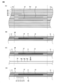
- FIG. 1 is a perspective view of a multilayer ceramic capacitor 100 according to a first embodiment, showing the multilayer ceramic capacitor 100 from a first main surface 1A side.
- 1 is a perspective view of a multilayer ceramic capacitor 100, showing the multilayer ceramic capacitor 100 from the second main surface 1B side.
- 1A is a cross-sectional view of the multilayer ceramic capacitor 100, showing a cross section of the portion XX indicated by the dashed dotted line arrow in FIG. 1 is a cross-sectional view of a main portion of a multilayer ceramic capacitor 100.
- FIG. 5A to 5D are explanatory views showing steps in an example of a method for manufacturing the multilayer ceramic capacitor 100.
- 6(E) to (J) are continuations of FIG.
- FIG. 4 is a cross-sectional view of a multilayer ceramic capacitor 200 according to a second embodiment.
- 8A to 8D are explanatory diagrams showing steps in an example of a method for manufacturing the multilayer ceramic capacitor 200.
- 9(E) to (J) are continuations of FIG. 8(D), and are explanatory views showing steps in an example of a method for manufacturing the multilayer ceramic capacitor 200.
- each embodiment is an illustrative example of how the present invention can be implemented, and the present invention is not limited to the contents of the embodiment. It is also possible to combine the contents described in different embodiments, and the implementation in such cases is also included in the present invention.
- the drawings are intended to aid in understanding the specification, and may be drawn diagrammatically, and the dimensional ratios of the depicted components or between the components may not match the dimensional ratios of those components described in the specification. Components described in the specification may be omitted in the drawings, or the number of components may be omitted when drawn.
- Figures 1, 2, 3, and 4 each show a multilayer ceramic capacitor 100 according to the first embodiment.
- Figure 1 is a perspective view of the multilayer ceramic capacitor 100, showing the multilayer ceramic capacitor 100 from the first main surface 1A side.
- Figure 2 is also a perspective view of the multilayer ceramic capacitor 100, showing the multilayer ceramic capacitor 100 from the second main surface 1B side.
- Figure 3 is a cross-sectional view of the multilayer ceramic capacitor 100, showing a cross section of the X-X portion indicated by the dashed dotted line arrow in Figure 1(A).
- Figure 4 is a cross-sectional view of a main portion of the multilayer ceramic capacitor 100.
- the drawings show the height direction T, length direction L, and width direction W of the multilayer ceramic capacitor 100, and these directions may be referred to in the following description.
- the stacking direction of the ceramic layers 1a which will be described later, is the height direction T of the multilayer ceramic capacitor 100.
- the multilayer ceramic capacitor 100 includes a ceramic body 1.
- the ceramic body 1 is a rectangular parallelepiped and has a first main surface 1A and a second main surface 1B that face each other in the height direction T, a first end surface 1C and a second end surface 1D that face each other in the length direction L, and a first side surface 1E and a second side surface 1F that face each other in the width direction W.
- the dimensions of the ceramic body 1 are arbitrary, but for example, it is also preferable that one of the dimensions in the length direction L and the width direction W is 1.0 mm or less and the other is 0.5 mm or less. It is also preferable that the dimension in the height direction T is 0.1 mm or less.
- the R dimension of the ridges where the first main surface 1A, which is the mounting surface, meets the first end surface 1C, the first side surface 1E, the second end surface 1D, and the second side surface 1F is large, so that even if the first main surface of the ceramic body collides with the substrate or an electrode formed on the substrate during mounting, the occurrence of cracks in the ceramic body 1 is suppressed.
- the ceramic body 1 is composed of a laminate of a ceramic layer 1a, a first internal electrode 2, a second internal electrode 3, and a dummy internal electrode 4.
- the ceramic layer 1a, the first internal electrode 2, the second internal electrode 3, and the dummy internal electrode 4 are laminated in the height direction T of the ceramic body 1.
- the dummy internal electrode 4 is an electrode that is provided not primarily to form capacitance, but as an underlying external electrode for the first external electrode 5 and the second external electrode 6.
- the ceramic body 1 may be made of any material, and may be, for example, a dielectric ceramic containing BaTiO 3 as a main component. However, instead of BaTiO 3 , a dielectric ceramic containing another material as a main component, such as CaTiO 3 , SrTiO 3 , or CaZrO 3 , may be used.
- the thickness of the ceramic layer 1a is arbitrary, but for example, it can be about 0.3 ⁇ m to 2.0 ⁇ m in the effective capacitance formation area where the first internal electrode 2 and the second internal electrode 3 are formed.
- the number of ceramic layers 1a is arbitrary, but for example, in the effective capacitance formation region where the first internal electrode 2 and the second internal electrode 3 are formed, it can be about 1 to 6000 layers.
- a protective layer (outer layer) is provided that does not have the first internal electrode 2 and the second internal electrode 3 and is composed only of the ceramic layer 1a.
- a dummy internal electrode 4 is formed in the protective layer.
- the thickness of the protective layer is arbitrary, but can be, for example, about 5 ⁇ m to 150 ⁇ m.
- the thickness of the ceramic layer 1a of the protective layer may be greater than the thickness of the ceramic layer 1a in the effective region of capacitance formation where the first internal electrode 2 and the second internal electrode 3 are formed.
- the material of the ceramic layer 1a of the protective layer may be different from the material of the ceramic layer 1a in the effective region.
- the first internal electrode 2 extends in the length direction L of the ceramic body 1, with one end extending to a first end face 1C of the ceramic body 1.
- the second internal electrode 3 extends in the length direction L of the ceramic body 1, with one end extending to a second end face 1D of the ceramic body 1.
- the dummy internal electrode 4 provided as an underlying external electrode for the first external electrode 5 and the second external electrode 6 has a smaller dimension in the length direction L than the first internal electrode 2 and the second internal electrode 3.
- One end of the dummy internal electrode 4 is extended to either the first end face 1C or the second end face 1D of the ceramic body 1.
- the dummy internal electrode 4 disposed closest to the first main surface 1A of the ceramic body 1 is exposed to the first main surface 1A of the ceramic body 1.
- At least the dummy internal electrodes 4 are arranged in the first external electrode 5 and the second external electrode 6 closest to the first main surface 1A of the ceramic body 1, and there should be one layer exposed on the first main surface of the ceramic body 1.
- the main components (metal components) of the first internal electrode 2, second internal electrode 3, and dummy internal electrode 4 may be made of any material, but in this embodiment, Ni is used. However, other metals such as Cu, Ag, Pd, and Au may be used instead of Ni. Furthermore, Ni, Cu, Ag, Pd, and Au may be alloyed with other metals.
- the first internal electrode 2, second internal electrode 3, and dummy internal electrode 4 may contain other components such as ceramics in addition to the metal components.
- the thickness of the first internal electrode 2, the second internal electrode 3, and the dummy internal electrode 4 is arbitrary, but can be, for example, about 0.3 ⁇ m to 1.5 ⁇ m.
- a first external electrode 5 and a second external electrode 6 are formed on the outer surface of the ceramic body 1.
- the first external electrode 5 is formed in an L-shape on the first end surface 1C and the first main surface 1A
- the second external electrode 6 is formed in an L-shape on the second end surface 1D and the first main surface 1A.
- the first external electrode 5 is electrically connected to the first internal electrode 2 at the first end surface 1C.
- the second external electrode 6 is electrically connected to the second internal electrode 3 at the second end surface 1D.
- the first external electrode 5 and the second external electrode 6 have the same multi-layer structure.
- the first external electrode 5 and the second external electrode 6 have, in order from the bottom, a base external electrode, a Cu-plated external electrode layer 7 formed on the outside of the base external electrode, a Ni-plated external electrode layer 8 formed on the outside of the Cu-plated external electrode layer 7, and an Au-plated external electrode layer 9 formed on the outside of the Ni-plated external electrode layer 8.
- the structure and materials of the first external electrode 5 and the second external electrode 6 are arbitrary and are not limited to these structures and materials.
- the dimensions such as thickness, width, and length of the first external electrode 5 and the second external electrode 6 are also arbitrary and can be freely set. In particular, various variations can be adopted for the number of layers, materials, dimensions, etc. of the plated external electrode layers.
- the base external electrode is an electrode that serves as a base when forming a plated external electrode layer on its outside.
- the base external electrode of the first external electrode 5 is composed of the ends of the first internal electrode 2 and dummy internal electrode 4 drawn out to the first end surface 1C, and the main surface of the dummy internal electrode 4 exposed to the first main surface 1A.
- FIG. 3 illustrates a structure in which the first external electrode 5 has four layers of dummy internal electrodes 4 as base external electrodes, the upper main surface of the dummy internal electrode 4 arranged closest to the first main surface 1A is exposed to the first main surface 1A, and the ends of the remaining three layers of dummy internal electrodes 4 are drawn out to the first end surface 1C.
- the number of layers of the dummy internal electrodes 4 of the first external electrode 5 is arbitrary, and it is sufficient that the first external electrode 5 has at least one layer arranged closest to the first main surface 1A of the ceramic body 1 and whose upper main surface is exposed to the outside from the first main surface 1A of the ceramic body 1.
- the base external electrode of the second external electrode 6 is composed of the ends of the second internal electrode 3 and the dummy internal electrode 4 drawn out to the second end surface 1D, and the main surface of the dummy internal electrode 4 exposed to the first main surface 1A.
- the second external electrode 6 has four layers of dummy internal electrodes 4 as base external electrodes, the upper main surface of the dummy internal electrode 4 arranged closest to the first main surface 1A is exposed to the first main surface 1A, and the ends of the remaining three layers of dummy internal electrodes 4 are drawn out to the second end surface 1D.
- the number of layers of the dummy internal electrodes 4 of the second external electrode 6 is arbitrary, and it is sufficient that the second external electrode 6 has at least one layer arranged closest to the first main surface 1A of the ceramic body 1 and whose upper main surface is exposed to the outside from the first main surface 1A of the ceramic body 1.
- the end of the first internal electrode 2 extended to the first end face 1C of the ceramic body 1 and the end of the second internal electrode 3 extended to the second end face 1D of the ceramic body 1 are also part of the underlying external electrodes of the first external electrode 5 and the second external electrode 6.
- the end of the first internal electrode 2 and the end of the second internal electrode 3 are not shown as part of the first external electrode 5 and the second external electrode 6 to avoid complicating the drawings (the leading lines from the reference numeral "5" indicating the first external electrode 5 and the reference numeral "6" indicating the second external electrode 6 have been omitted).
- the base external electrodes of the first external electrode 5 and the second external electrode 6 function as a base for forming a Cu-plated external electrode layer 7 on the outside thereof.
- the end of the first internal electrode 2 extended to the first end face 1C, the end of the dummy internal electrode 4, the end of the second internal electrode 3 extended to the second end face 1D, and the end of the dummy internal electrode 4 are also part of the base external electrodes of the first external electrode 5 and the second external electrode 6.
- the ends of the multiple linear first internal electrodes 2 and the ends of the dummy internal electrodes 4 extending in the width direction W are exposed, and on the second end face 1D, the ends of the multiple linear second internal electrodes 3 and the ends of the dummy internal electrodes 4 extending in the width direction W are exposed at intervals (with the ends of the linear ceramic layers 1a extending in the width direction W sandwiched between them).
- the ends of the first internal electrodes 2, the ends of the second internal electrodes 3, and the ends of the dummy internal electrodes 4 are spaced apart, they function as a base when forming the plated external electrode layer.
- the first external electrode 5 and the second external electrode 6 each have a Cu-plated external electrode layer 7 on the outside of the base external electrode.
- the Cu-plated external electrode layer 7 mainly functions to improve moisture resistance. It is also preferable that the Cu-plated external electrode layer 7 contains Ni. In this case, dissolution of the external electrode layer into the solder can be suppressed.
- the first external electrode 5 and the second external electrode 6 each have a Ni-plated external electrode layer 8 on the outside of the Cu-plated external electrode layer 7.
- the Ni-plated external electrode layer 8 mainly functions to improve solder heat resistance and bondability. It is also preferable that the Ni-plated external electrode layer 8 contains P. In this case, the mechanical strength of the external electrode layer can be improved.
- the first external electrode 5 and the second external electrode 6 have an Au-plated external electrode layer 9 on the outside of the Ni-plated external electrode layer 8.
- the Au-plated external electrode layer 9 mainly serves the function of improving the wettability of the external electrode layer to the solder.
- the R dimensions of the ridgeline E11 where the first main surface 1A and the first end surface 1C meet, the ridgeline E12 where the first main surface 1A and the first side surface 1E meet, the ridgeline E13 where the first main surface 1A and the second end surface 1D meet, and the ridgeline E14 where the first main surface 1A and the second side surface 1F meet are larger than the R dimensions of the ridgeline E21 where the second main surface 1B and the first end surface 1C meet, the ridgeline E22 where the second main surface 1B and the first side surface 1E meet, the ridgeline E23 where the second main surface 1B and the second end surface 1D meet, and the ridgeline E24 where the second main surface 1B and the second side surface 1F meet.
- the manufacturing process includes a separate step of increasing the R dimension for ridgeline E11 where first main surface 1A meets first end surface 1C, ridgeline E12 where first main surface 1A meets first side surface 1E, ridgeline E13 where first main surface 1A meets second end surface 1D, and ridgeline E14 where first main surface 1A meets second side surface 1F.
- the manufacturing process does not include a step of increasing the R dimension for ridgeline E21 where second main surface 1B meets first end surface 1C, ridgeline E22 where second main surface 1B meets first side surface 1E, ridgeline E23 where second main surface 1B meets second end surface 1D, and ridgeline E24 where second main surface 1B meets second side surface 1F.
- the first main surface 1A of the ceramic body 1, which is provided with the first external electrode 5 and the second external electrode 6, is the mounting surface for the substrate (as described above, “substrate” includes “substrate-like objects”).
- the multilayer ceramic capacitor 100 has a large R dimension (large roundness) for the ridgeline E11 where the first main surface 1A and the first end surface 1C meet, the ridgeline E12 where the first main surface 1A and the first side surface 1E meet, the ridgeline E13 where the first main surface 1A and the second end surface 1D meet, and the ridgeline E14 where the first main surface 1A and the second side surface 1F meet, which are provided on the mounting surface side.
- the multilayer ceramic capacitor 100 is placed (placed) on a substrate for mounting, even if these ridgelines collide with the substrate or electrodes formed on the substrate, the impact is mitigated, and the occurrence of cracks in the ceramic body 1 is suppressed.
- each of the R dimensions of the ridgeline E11 where the first main surface 1A and the first end surface 1C meet, the ridgeline E12 where the first main surface 1A and the first side surface 1E meet, the ridgeline E13 where the first main surface 1A and the second end surface 1D meet, and the ridgeline E14 where the first main surface 1A and the second side surface 1F meet is, for example, about 1 ⁇ m or more and 10 ⁇ m or less. This is because if it is less than 1 ⁇ m, the effect of suppressing the occurrence of cracks and the like in the ceramic body 1 is small.
- the process of increasing the R dimensions of each of these ridgelines takes time, reducing the productivity of the multilayer ceramic capacitor.
- the R dimensions of the ridgeline E21 where the second main surface 1B and the first end surface 1C meet, the ridgeline E22 where the second main surface 1B and the first side surface 1E meet, the ridgeline E23 where the second main surface 1B and the second end surface 1D meet, and the ridgeline E24 where the second main surface 1B and the second side surface 1F meet are each less than about 1 ⁇ m, for example. In this case, there is no need to provide a separate process for increasing the R dimensions of these ridgelines.
- the multilayer ceramic capacitor 100 of this embodiment has a corner C11 where the first main surface 1A, the first end surface 1C, and the first side surface 1E meet, a corner C12 where the first main surface 1A, the first side surface 1E, and the second end surface 1D meet, a corner C13 where the first main surface 1A, the second end surface 1D, and the second side surface 1F meet, a corner C14 where the first main surface 1A, the second side surface 1F, and the first end surface 1C meet, and a corner C15 where the first main surface 1A, the second end surface 1D, and the second side surface 1F meet.
- the R dimension of corner C14 where surface 1C meets is larger than the R dimensions of corner C21 where second main surface 1B, first end surface 1C and first side surface 1E meet, corner C22 where second main surface 1B, first side surface 1E and second end surface 1D meet, corner C23 where second main surface 1B, second end surface 1D and second side surface 1F meet, and corner C24 where second main surface 1B, second side surface 1F and first end surface 1C meet.
- the R dimensions of the ridgeline E11 where the first main surface 1A and the first end surface 1C meet, the ridgeline E12 where the first main surface 1A and the first side surface 1E meet, the ridgeline E13 where the first main surface 1A and the second end surface 1D meet, and the ridgeline E14 where the first main surface 1A and the second side surface 1F meet are larger than the R dimensions of the ridgeline E21 where the second main surface 1B and the first end surface 1C meet, the ridgeline E22 where the second main surface 1B and the first side surface 1E meet, the ridgeline E23 where the second main surface 1B and the second end surface 1D meet, and the ridgeline E24 where the second main surface 1B and the second side surface 1F meet.
- the R dimension of the corner where two ridgelines with a large R dimension intersect is larger than the R dimension of the corner where two ridgelines with a small R dimension intersect.
- the laminated ceramic capacitor 100 has corners C11 on the mounting surface where the first main surface 1A, first end surface 1C, and first side surface 1E meet, corner C12 where the first main surface 1A, first side surface 1E, and second end surface 1D meet, corner C13 where the first main surface 1A, second end surface 1D, and second side surface 1F meet, and corner C14 where the first main surface 1A, second side surface 1F, and first end surface 1C meet.
- the multilayer ceramic capacitor 100 of this embodiment has a plurality of embossed holes 10 formed on the second main surface 1B of the ceramic body 1.
- a plurality of embossed holes 10 of the same shape and dimensions are formed on the second main surface 1B of the ceramic body 1 in a state aligned in the length direction L and width direction W.
- an embossed hole refers to a bottomed hole with a concave surface.
- the concave surface may be hemispherical or non-hemispherical.
- the method of forming the embossed holes 10 is also arbitrary. Whether or not embossed holes 10 are formed in the second main surface 1B can be easily confirmed by comparing with other surfaces of the ceramic body 1 (such as the first main surface 1A).
- the second main surface 1B of the ceramic body 1 is the surface that is sucked by, for example, the nozzle of a mounter device during mounting, and is the surface that may be subjected to impact by the nozzle.
- the multilayer ceramic capacitor 100 of this embodiment since a plurality of embossed holes 10 are formed in the second main surface 1B of the ceramic body 1, even if an impact is applied by a nozzle or the like, the multilayer ceramic capacitor 100 is resistant to the impact, and the occurrence of cracks in the ceramic body 1 is suppressed. Note that if the embossed holes 10 are minute and the depth is contained within one to several tens of ceramic layers 1a, the impact resistance of the ceramic body 1 can be improved satisfactorily. However, if the depth of the embossed holes 10 is too large, it may conversely reduce the overall strength of the ceramic body 1, so it is necessary that the depth of the embossed holes 10 is not too large.
- the multilayer ceramic capacitor 100 of this embodiment can be manufactured, for example, by the method shown in Figures 5(A) to 6(J).
- a ceramic green sheet 11a is prepared for producing the ceramic layer 1a of the ceramic body 1, as shown in FIG. 5(A).
- the ceramic green sheet 11a is prepared as a mother ceramic green sheet 50 in which a large number of ceramic green sheets 11a are arranged in a matrix in order to manufacture a large number of multilayer ceramic capacitors 100 at once.
- dielectric ceramic powder, binder resin, solvent, etc. are prepared and then wet-mixed to create ceramic slurry.
- the ceramic slurry is applied in sheet form onto the carrier film using a die coater, gravure coater, microgravure coater, etc., and dried to produce the mother ceramic green sheet 50.
- a conductive paste 12 for forming the first internal electrode 2, a conductive paste 13 for forming the second internal electrode 3, and a conductive paste 14 for forming the dummy internal electrode 4, which have been prepared in advance, are applied (e.g., printed) in a desired pattern shape to the main surface of a predetermined ceramic green sheet 11a in the mother ceramic green sheet 50.
- the conductive paste may be, for example, a mixture of a solvent, a binder resin, a metal powder (e.g., Ni powder), etc.
- the mother ceramic green sheets 50 are stacked in a predetermined order and pressed together to produce a mother unsintered ceramic body 60 in which numerous unsintered ceramic bodies 11 are arranged in a matrix.
- a jig 70 is prepared with multiple protrusions 70a formed on its upper main surface.
- the lower main surface of the mother unsintered ceramic body 60 is then pressed against the protrusions 70a of the jig 70.
- multiple embossed holes 10 are formed in the second main surface 1B of each unsintered ceramic body 11 of the mother unsintered ceramic body 60.
- the mother unsintered ceramic body 60 is cut into individual unsintered ceramic bodies 11.
- the unsintered ceramic body 11 is fired with a predetermined profile to produce the ceramic body 1 shown in FIG. 6(F).
- a conductive paste 12 is fired at the same time to form a first internal electrode 2
- a conductive paste 13 is fired at the same time to form a second internal electrode 3
- a conductive paste 14 is fired at the same time to form a dummy internal electrode 4.
- a jig 80 is prepared.
- the second main surface 1B of the ceramic body 1 is fixed to the upper main surface of the jig 80.
- the first main surface 1A of the ceramic body 1 is scraped off, for example by sandblasting, so that the upper main surface of the dummy internal electrode 4 that is disposed closest to the first main surface 1A of the ceramic body 1 is exposed to the first main surface 1A of the ceramic body 1.
- the ridgeline E11 where the first main surface 1A and the first end surface 1C meet, the ridgeline E12 where the first main surface 1A and the first side surface 1E meet, the ridgeline E13 where the first main surface 1A and the second end surface 1D meet, and the ridgeline E14 where the first main surface 1A and the second side surface 1F meet are each cut away, and the ridgeline E11 where the first main surface 1A and the first end surface 1C meet, the ridgeline E12 where the first main surface 1A and the first side surface 1E meet, and the ridgeline E14 where the first main surface 1A and the first
- the R dimensions of the ridgeline E13 where the first main surface 1A and the second end surface 1D meet, and the ridgeline E14 where the first main surface 1A and the second side surface 1F meet are larger (more rounded) than the R dimensions of the ridgeline E21 where the second main surface 1B and the first end surface 1C meet, the ridgeline E22 where the second main surface 1
- the ends of the first internal electrode 2, the second internal electrode 3, and the dummy internal electrode 4 extended to the first end face 1C and the second end face 1D, and the upper main surface of the dummy internal electrode 4 exposed to the first main surface 1A are used as base external electrodes, and a predetermined catalyst is applied to the surfaces of these base external electrodes as necessary, followed by electroless plating to form a Cu-plated external electrode layer 7.
- a specific catalyst is applied to the outside of the Cu-plated external electrode layer 7 as necessary, and then electroless plating is performed to form the Ni-plated external electrode layer 8.
- the first external electrode 5 is formed in an L-shape on the first end face 1C and first main face 1A of the ceramic body 1
- the second external electrode 6 is formed in an L-shape on the second end face 1D and first main face 1A of the ceramic body 1, completing the multilayer ceramic capacitor 100 according to the first embodiment.
- FIG. 7 shows a multilayer ceramic capacitor 200 according to the second embodiment. Note that FIG. 7 is a cross-sectional view of the multilayer ceramic capacitor 200.
- the multilayer ceramic capacitor 200 according to the second embodiment is a modified version of the multilayer ceramic capacitor 100 according to the first embodiment described above.
- a dummy internal electrode 4 was used as part of the underlying external electrodes for the first external electrode 5 and the second external electrode 6.
- the multilayer ceramic capacitor 200 changes this by omitting the dummy internal electrode 4.
- a NiCr thin film layer 27 is formed by sputtering as the underlying external electrode for the first external electrode 25 and the second external electrode 26.
- the NiCr thin film layer 27 has high adhesion to the ceramic body 1, and serves as an excellent underlying external electrode for the first external electrode 25 and the second external electrode 26.
- the plated external electrode layers of the first external electrode 5 and the second external electrode 6 were provided in the order of Cu-plated external electrode layer 7, Ni-plated external electrode layer 8, and Au-plated external electrode layer 9 on the outside of the base external electrode.
- the other configurations of the multilayer ceramic capacitor 200 are the same as those of the multilayer ceramic capacitor 100.
- the R dimensions of the ridgeline E11 where the first main surface 1A and the first end surface 1C meet, the ridgeline E12 where the first main surface 1A and the first side surface 1E meet, the ridgeline E13 where the first main surface 1A and the second end surface 1D meet, and the ridgeline E14 where the first main surface 1A and the second side surface 1F meet are larger than the R dimensions of the ridgeline E21 where the second main surface 1B and the first end surface 1C meet, the ridgeline E22 where the second main surface 1B and the first side surface 1E meet, the ridgeline E23 where the second main surface 1B and the second end surface 1D meet, and the ridgeline E24 where the second main surface 1B and the second side surface 1F meet. Therefore, even if these ridges collide with the substrate or electrodes formed on the substrate when the multilayer ceramic capacitor 200 is placed on a substrate for mounting, the impact is mitigated, preventing cracks from occurring in the
- the multilayer ceramic capacitor 200 of this embodiment can be manufactured, for example, by the method shown in Figures 8(A) to 9(J).
- a ceramic green sheet 11a is prepared for producing the ceramic layer 1a of the ceramic body 1, as shown in FIG. 8(A).
- the ceramic green sheet 11a is prepared as a mother ceramic green sheet 50 for manufacturing a large number of multilayer ceramic capacitors 100 at once.
- a conductive paste 12 for forming the first internal electrode 2 and a conductive paste 13 for forming the second internal electrode 3, which have been prepared in advance, are applied in a desired pattern shape to the main surface of a predetermined ceramic green sheet 11a in the mother ceramic green sheet 50. Note that since the multilayer ceramic capacitor 200 does not have a dummy internal electrode, no conductive paste for forming a dummy internal electrode is applied.
- the mother ceramic green sheets 50 are stacked in a predetermined order and pressed together to produce the mother unsintered ceramic body 60.
- the lower main surface of the mother unsintered ceramic body 60 is pressed against a jig 70 having multiple protrusions 70a formed on its upper main surface, and as shown in FIG. 8(D), multiple embossed holes 10 are formed in the second main surface 1B of each unsintered ceramic body 11.
- the mother unsintered ceramic body 60 is cut into individual unsintered ceramic bodies 11.
- the unsintered ceramic body 11 is fired with a predetermined profile to produce the ceramic body 1 shown in Figure 9 (F).
- a jig 80 is prepared.
- the second main surface 1B of the ceramic body 1 is fixed to the upper main surface of the jig 80.
- sandblasting is performed to remove the ridgeline E11 where the first main surface 1A and the first end surface 1C meet, the ridgeline E12 where the first main surface 1A and the first side surface 1E meet, the ridgeline E13 where the first main surface 1A and the second end surface 1D meet, and the ridgeline E14 where the first main surface 1A and the second side surface 1F meet, thereby increasing their R dimensions.
- a NiCr thin film layer 27 is formed by sputtering as an underlying external electrode for the first external electrode 25 and the second external electrode 26.
- a specified catalyst is applied to the outside of the NiCr thin film layer 27, which is the base external electrode of the first external electrode 25 and the second external electrode 26, if necessary, and then electroless plating is performed to form the Ni-plated external electrode layer 28.
- a predetermined catalyst is applied to the outside of the Ni-plated external electrode layer 28 if necessary, and then electroless plating is performed to form an Au-plated external electrode layer 29.
- an L-shaped first external electrode 25 is formed on the first end face 1C and first main surface 1A of the ceramic body 1
- an L-shaped second external electrode 26 is formed on the second end face 1D and first main surface 1A of the ceramic body 1, completing the multilayer ceramic capacitor 200 according to the second embodiment.
- a process was provided for increasing the R dimensions of ridgeline E11 where the first main surface 1A and the first end surface 1C meet, ridgeline E12 where the first main surface 1A and the first side surface 1E meet, ridgeline E13 where the first main surface 1A and the second end surface 1D meet, and ridgeline E14 where the first main surface 1A and the second side surface 1F meet, but a process was not provided for increasing the R dimensions of ridgeline E21 where the second main surface 1B and the first end surface 1C meet, ridgeline E22 where the second main surface 1B and the first side surface 1E meet, ridgeline E23 where the second main surface 1B and the second end surface 1D meet, and ridgeline E24 where the second main surface 1B and the second side surface 1F meet.
- the R dimensions of the ridgeline E12 where the surface 1A meets the first side surface 1E, the ridgeline E13 where the first main surface 1A meets the second end surface 1D, and the ridgeline E14 where the first main surface 1A meets the second side surface 1F may be larger than the R dimensions of the ridgeline E21 where the second main surface 1B meets the first end surface 1C, the ridgeline E22 where the second main surface 1B meets the first side surface 1E, the ridgeline E23 where the second main surface 1B meets the second end surface 1D, and the ridgeline E24 where the second main surface 1B meets the second side surface 1F.
- the embossed holes 10 are formed in the second main surface 1B of the ceramic body 1, but in the multilayer ceramic capacitor of the present invention, the embossed holes 10 are not an essential component and can be omitted.
- the multilayer ceramic capacitor according to one embodiment of the present invention is as described in the "Means for solving the problems" section.
- the R dimension of the ridges where the first main surface meets the first end face, the second end face, the first side face, and the second side face is 1 ⁇ m or more and 10 ⁇ m or less. If it is less than 1 ⁇ m, the effect of suppressing the occurrence of cracks in the ceramic body when these ridges collide with a substrate or the like is small. Also, if it exceeds 10 ⁇ m, the process of increasing the R dimension of each of these ridges takes time, reducing the productivity of the multilayer ceramic capacitor.
- the R dimension of the corner where the first main surface, the first end face and the first side surface meet, the corner where the first main surface, the first side surface and the second end face meet, the corner where the first main surface, the second end face and the second side surface meet, and the corner where the first main surface, the second side surface and the first end face meet is larger than the R dimension of the corner where the second main surface, the first end face and the first side surface meet, the corner where the second main surface, the first side surface and the second end face meet, the corner where the second main surface, the second end face and the second side surface meet, and the corner where the second main surface, the second side surface and the first end face meet.
- the corners on the mounting surface where the first main surface, the first end surface, and the first side surface meet, the corners where the first main surface, the first side surface, and the second end surface meet, the corners where the first main surface, the second end surface, and the second side surface meet, and the corners where the first main surface, the second side surface, and the first end surface meet have large R dimensions. Therefore, even if these corners collide with the substrate or an electrode formed on the substrate when the multilayer ceramic capacitor is placed on a substrate or the like for mounting, the impact is mitigated, and the occurrence of cracks in the ceramic body is suppressed.
- a plurality of embossed holes are formed on the second main surface of the ceramic body.
- the ceramic body is resistant to the impact and the occurrence of cracks or the like in the ceramic body is suppressed.
- the first external electrode and the second external electrode each include a base external electrode and at least one plated external electrode layer formed on the outside of the base external electrode.
- the plated external electrode layer can be easily formed on the outside of the base external electrode by, for example, electroless plating.
- the base external electrode includes a dummy internal electrode that is smaller in length than the first internal electrode and the second internal electrode and is exposed on the first main surface of the ceramic body. In this case, it is possible to easily form the first external electrode and the second external electrode that have a relatively large area on the first main surface of the ceramic body.
- the dummy internal electrode, the first internal electrode, and the second external electrode are formed from the same material. In this case, there is no need to prepare a separate material to form the dummy internal electrode, which is the base external electrode, improving the productivity of the multilayer ceramic capacitor.
- the dummy internal electrode is mainly composed of Ni.
- the ceramic body, the first internal electrode, the second external electrode, and the dummy internal electrode can be easily produced by so-called simultaneous firing.
- the base external electrode is a thin film.
- the base external electrode can be easily formed, for example, by sputtering.
- the thin film is mainly composed of NiCr. In this case, it has high adhesion to the ceramic body and serves as an excellent base external electrode for the first and second external electrodes.
- the plated external electrode layer includes at least one selected from a Cu-plated external electrode layer, a Ni-plated external electrode layer, and an Au-plated external electrode layer.
- various functions are exerted in each plated external electrode layer, and excellent first and second external electrodes can be formed.
- the plated external electrode layer includes a Ni-plated external electrode layer formed on the outside of the base external electrode, and an Au-plated external electrode layer formed on the outside of the Ni-plated external electrode layer.
- the Ni-plated external electrode layer can mainly function to improve the solder heat resistance and bondability
- the Au-plated external electrode layer 9 can mainly function to improve the wettability of the external electrode layer to the solder.
- the plated external electrode layer includes a Cu-plated external electrode layer formed on the outside of the base external electrode, a Ni-plated external electrode layer formed on the outside of the Cu-plated external electrode layer, and an Au-plated external electrode layer formed on the outside of the Ni-plated external electrode layer.
- the Cu-plated external electrode layer 7 can mainly function to improve moisture resistance
- the Ni-plated external electrode layer can mainly function to improve solder heat resistance and bondability
- the Au-plated external electrode layer 9 can mainly function to improve the wettability of the external electrode layer to solder.
- the Ni-plated external electrode layer contains P. In this case, the mechanical strength of the external electrode layer is improved.
- the Cu-plated external electrode layer contains Ni. In this case, dissolution of the external electrode layer into the solder can be suppressed.
- one of the lengthwise dimension and widthwise dimension is 1.0 mm or less, and the other is 0.5 mm or less. It is also preferable that the heightwise dimension is 0.1 mm or less. Even when the present invention is applied to a multilayer ceramic capacitor that is miniaturized and thinned in this way, the R dimension of the ridges where the first main surface, which is the mounting surface, meets the first end face, first side face, second end face, and second side face is large, so that even if these ridges collide with the substrate or electrodes formed on the substrate during mounting, the occurrence of cracks in the ceramic body is suppressed.
- Ceramic body 1a Ceramic layer 1A: First main surface 1B: Second main surface 1C: First end surface 1D: Second end surface 1E: First side surface 1F: Second side surface 2: First internal electrode 3: Second internal electrode 4: Dummy internal electrode 5: First external electrode 6: Second external electrode 7: Cu-plated external electrode layer 8, 28: Ni-plated external electrode layer 9, 29: Au-plated external electrode layer 27: NiCr thin film layer (base external electrode) 10: Embossed hole
Abstract
Provided is a laminated ceramic capacitor whereby cracking or the like is less likely to occur in a ceramic body. Provided is a laminated ceramic capacitor comprising: a ceramic body, in which a plurality of ceramic layers, a plurality of first internal electrodes, and a plurality of second internal electrodes are laminated in the height direction, and which has a first principal surface and a second principal surface that face one another in the height direction, a first end surface and a second end surface that face one another in the length direction orthogonal to the height direction, and a first side surface and a second side surface that face one another in the width direction orthogonal to the height direction and to the length direction; and a first external electrode and a second external electrode that are formed on an outer surface of the ceramic body. The first internal electrodes are drawn out to the first end surface and electrically connected with the first external electrode; and the second internal electrodes are drawn out to the second end surface and electrically connected with the second external electrode. When a cross-section parallel to the first side surface and the second side surface is viewed, the first external electrode is formed in an L-shape on the first end surface and the first principal surface, and the second external electrode is formed in an L-shape on the second end surface and the first principal surface; and an R-dimension of a ridge line where the first principal surface and the first end surface, the first side surface, the second end surface, and the second side surface are in contact is greater than an R-dimension of a ridge line where the second principal surface and the first end surface, the first side surface, the second end surface, and the second side surface are in contact.
Description
本発明は、積層セラミックコンデンサに関する。
The present invention relates to a multilayer ceramic capacitor.
積層セラミックコンデンサが、電子機器、電気機器をはじめとする種々の機器(以下「電子機器等」という)に、広く使用されている。たとえば、特許文献1(特開2000-100647号公報)に、典型的な構造の積層セラミックコンデンサが開示されている。
Multilayer ceramic capacitors are widely used in a variety of devices, including electronic devices and electrical devices (hereinafter referred to as "electronic devices, etc."). For example, Patent Document 1 (JP 2000-100647 A) discloses a multilayer ceramic capacitor with a typical structure.
近時、電子機器等の小型化や高機能化が、急速に進んでいる。電子機器等の小型化によって、電子部品によって構成される電子回路を収納する電子機器等の内部容積(空間容積)が極めて小さくなってきている。また、電子機器等の高機能化によって、電子回路を構成するのに必要な電子部品の個数が急増している。
In recent years, electronic devices have become smaller and more functional. As a result of the miniaturization of electronic devices, the internal volume (spatial volume) of electronic devices that houses electronic circuits made up of electronic components has become extremely small. Furthermore, as electronic devices become more functional, the number of electronic components required to make up an electronic circuit is rapidly increasing.
そのため、電子機器等の小型化や高機能化にともない、電子回路を構成する電子部品に対しても、小型化が求められている。たとえば、積層セラミックコンデンサでは、セラミック素体が数十μmの厚さからなる、極めて薄型化された製品が実用化されている。
As electronic devices become smaller and more functional, there is a demand for smaller electronic components that make up electronic circuits. For example, extremely thin multilayer ceramic capacitors with ceramic bodies just a few tens of micrometers thick are now in practical use.
上述したように、電子機器等の小型化や高機能化にともない、電子部品の小型化、特に薄型化が求められているが、積層セラミックコンデンサの場合、薄型化にともない、外力に対する機械的強度の低下が問題となっている。
As mentioned above, as electronic devices become smaller and more functional, there is a demand for smaller electronic components, particularly thinner ones. However, in the case of multilayer ceramic capacitors, the thinner they are, the lower their mechanical strength against external forces becomes an issue.
一方、積層セラミックコンデンサは、たとえば、次に示すリフローはんだ工程によって、基板や、基板に準ずるもの(以下においては両者を合わせて「基板」という)に実装されることが多い。
On the other hand, multilayer ceramic capacitors are often mounted on circuit boards or circuit board equivalents (hereafter both are collectively referred to as "circular boards") using the reflow soldering process described below.
まず、実装の相手先である基板を用意する。基板の主面には電極が形成されており、電極の表面には、予めクリームはんだが塗布されている。次に、ノズルを備えたマウンター装置を用意する。そして、ノズルで積層セラミックコンデンサの天面(第2主面)を吸着したうえで、ノズルを移動させることによって、積層セラミックコンデンサの底面(第1主面)を、基板のクリームはんだが塗布された1対の電極上に配置(プレーシング)する。次に、積層セラミックコンデンサが配置された基板を加熱し、クリームはんだを溶融させ、続いて全体を冷却し、クリームはんだを再び固化させて、積層セラミックコンデンサを基板の電極に実装する。
First, the substrate on which the capacitor will be mounted is prepared. Electrodes are formed on the main surface of the substrate, and cream solder has already been applied to the surfaces of the electrodes. Next, a mounter device equipped with a nozzle is prepared. The top surface (second main surface) of the multilayer ceramic capacitor is then attracted to the nozzle, and the nozzle is then moved to place (place) the bottom surface (first main surface) of the multilayer ceramic capacitor on the pair of electrodes of the substrate on which the cream solder has been applied. Next, the substrate on which the multilayer ceramic capacitor is mounted is heated to melt the cream solder, and then the entire substrate is cooled, causing the cream solder to solidify again, and the multilayer ceramic capacitor is mounted to the electrodes of the substrate.
このリフローはんだ工程において、ノズルで積層セラミックコンデンサを基板の電極上に配置するときに、セラミック素体の底面(第1主面)の外縁である稜線が、基板や、基板に形成された電極に衝突し、セラミック素体に、クラックなど(以下において、「ひび」、「割れ」、「欠け」などを総称して「クラックなど」という)が発生することが問題になっている。特に、薄型化され、外力に対する機械的強度の低下した積層セラミックコンデンサにおいて、実装のときなどに発生する、セラミック素体のクラックなどが極めて重大な問題になっている。
In this reflow soldering process, when the multilayer ceramic capacitor is placed on the electrode of the board with a nozzle, the ridge that forms the outer edge of the bottom surface (first main surface) of the ceramic element collides with the board or the electrode formed on the board, causing cracks and other problems in the ceramic element (hereinafter, "cracks and other problems" are collectively referred to as "cracking"). In particular, in multilayer ceramic capacitors that have been made thinner and have reduced mechanical strength against external forces, cracks in the ceramic element that occur during mounting and other such problems are an extremely serious issue.
そこで、本発明は、たとえば実装のときなどに、セラミック素体の底面(第1主面)の外縁である稜線が、基板や、基板に形成された電極などに衝突しても、セラミック素体にクラックなどが発生しにくい積層セラミックコンデンサを提供することを目的とする。
The present invention aims to provide a multilayer ceramic capacitor that is less likely to cause cracks in the ceramic body even if the ridge line, which is the outer edge of the bottom surface (first main surface) of the ceramic body, collides with the substrate or an electrode formed on the substrate, for example, during mounting.
上述した従来の課題を解決するために、本発明の一実施態様にかかる積層セラミックコンデンサは、複数のセラミック層と、複数の第1内部電極と、複数の第2内部電極とが高さ方向に積層され、高さ方向に対向する第1主面および第2主面と、高さ方向に直行する長さ方向に対向する第1端面および第2端面と、高さ方向および長さ方向に直行する幅方向に対向する第1側面および第2側面とを有するセラミック素体と、セラミック素体の外表面に形成された、第1外部電極および第2外部電極と、を備え、第1内部電極が、第1端面に引き出され、第1外部電極と電気的に接続され、第2内部電極が、第2端面に引き出され、第2外部電極と電気的に接続された積層セラミックコンデンサであって、第1側面および第2側面と平行な断面を見たとき、第1外部電極が、第1端面および第1主面に、L字形状に形成され、第2外部電極が、第2端面および第1主面に、L字形状に形成され、第1主面と、第1端面、第1側面、第2端面、第2側面とが接する稜線のR寸法が、第2主面と、第1端面、第1側面、第2端面、第2側面とが接する稜線のR寸法よりも、大きいものとする。
In order to solve the above-mentioned problems of the related art, a multilayer ceramic capacitor according to one embodiment of the present invention comprises a ceramic body in which a plurality of ceramic layers, a plurality of first internal electrodes, and a plurality of second internal electrodes are stacked in the height direction, the ceramic body having a first main surface and a second main surface opposing each other in the height direction, a first end surface and a second end surface opposing each other in the length direction perpendicular to the height direction, and a first side surface and a second side surface opposing each other in the width direction perpendicular to the height direction and the length direction, and a first external electrode and a second external electrode formed on the outer surface of the ceramic body, the first internal electrode being extended to the first end surface. A multilayer ceramic capacitor in which a first external electrode is drawn out to a second end face and electrically connected to the first external electrode, and a second internal electrode is drawn out to a second end face and electrically connected to the second external electrode, and when viewed in a cross section parallel to the first side face and the second side face, the first external electrode is formed in an L-shape on the first end face and the first main face, and the second external electrode is formed in an L-shape on the second end face and the first main face, and the R dimension of the ridge where the first main face meets the first end face, first side face, second end face, and second side face is larger than the R dimension of the ridge where the second main face meets the first end face, first side face, second end face, and second side face.
本発明の一実施態様にかかる積層セラミックコンデンサは、第1主面(底面;実装面)と、第1端面、第1側面、第2端面、第2側面とが接する稜線のR寸法が大きいため、実装のときに、これらの稜線が、基板や、基板に形成された電極などに衝突しても、セラミック素体にクラックなどが発生しにくい。
In one embodiment of the multilayer ceramic capacitor of the present invention, the R dimension of the ridges where the first main surface (bottom surface; mounting surface) meets the first end surface, first side surface, second end surface, and second side surface is large, so that even if these ridges collide with the substrate or electrodes formed on the substrate during mounting, cracks are unlikely to occur in the ceramic body.
以下、図面とともに、本発明を実施するための形態について説明する。
Below, we will explain the form for implementing the present invention with reference to the drawings.
なお、各実施形態は、本発明の実施の形態を例示的に示したものであり、本発明が実施形態の内容に限定されることはない。また、異なる実施形態に記載された内容を組合せて実施することも可能であり、その場合の実施内容も本発明に含まれる。また、図面は、明細書の理解を助けるためのものであって、模式的に描画されている場合があり、描画された構成要素または構成要素間の寸法の比率が、明細書に記載されたそれらの寸法の比率と一致していない場合がある。また、明細書に記載されている構成要素が、図面において省略されている場合や、個数を省略して描画されている場合などがある。
Note that each embodiment is an illustrative example of how the present invention can be implemented, and the present invention is not limited to the contents of the embodiment. It is also possible to combine the contents described in different embodiments, and the implementation in such cases is also included in the present invention. The drawings are intended to aid in understanding the specification, and may be drawn diagrammatically, and the dimensional ratios of the depicted components or between the components may not match the dimensional ratios of those components described in the specification. Components described in the specification may be omitted in the drawings, or the number of components may be omitted when drawn.
[第1実施形態]
図1、図2、図3、図4に、それぞれ、第1実施形態にかかる積層セラミックコンデンサ100を示す。ただし、図1は、積層セラミックコンデンサ100の斜視図であり、第1主面1A側から積層セラミックコンデンサ100を示している。図2も、積層セラミックコンデンサ100の斜視図であり、第2主面1B側から積層セラミックコンデンサ100を示している。図3は、積層セラミックコンデンサ100の断面図であり、図1(A)に一点鎖線矢印で示したX-X部分の断面を示している。図4は、積層セラミックコンデンサ100の要部断面図である。 [First embodiment]
Figures 1, 2, 3, and 4 each show a multilayerceramic capacitor 100 according to the first embodiment. However, Figure 1 is a perspective view of the multilayer ceramic capacitor 100, showing the multilayer ceramic capacitor 100 from the first main surface 1A side. Figure 2 is also a perspective view of the multilayer ceramic capacitor 100, showing the multilayer ceramic capacitor 100 from the second main surface 1B side. Figure 3 is a cross-sectional view of the multilayer ceramic capacitor 100, showing a cross section of the X-X portion indicated by the dashed dotted line arrow in Figure 1(A). Figure 4 is a cross-sectional view of a main portion of the multilayer ceramic capacitor 100.
図1、図2、図3、図4に、それぞれ、第1実施形態にかかる積層セラミックコンデンサ100を示す。ただし、図1は、積層セラミックコンデンサ100の斜視図であり、第1主面1A側から積層セラミックコンデンサ100を示している。図2も、積層セラミックコンデンサ100の斜視図であり、第2主面1B側から積層セラミックコンデンサ100を示している。図3は、積層セラミックコンデンサ100の断面図であり、図1(A)に一点鎖線矢印で示したX-X部分の断面を示している。図4は、積層セラミックコンデンサ100の要部断面図である。 [First embodiment]
Figures 1, 2, 3, and 4 each show a multilayer
なお、図面には、積層セラミックコンデンサ100の高さ方向T、長さ方向L、幅方向Wを示しており、以下の説明において、これらの方向に言及する場合がある。本実施形態においては、後述するセラミック層1aの積層方向を、積層セラミックコンデンサ100の高さ方向Tとしている。
The drawings show the height direction T, length direction L, and width direction W of the multilayer ceramic capacitor 100, and these directions may be referred to in the following description. In this embodiment, the stacking direction of the ceramic layers 1a, which will be described later, is the height direction T of the multilayer ceramic capacitor 100.
積層セラミックコンデンサ100は、セラミック素体1を備えている。セラミック素体1は、直方体からなり、高さ方向Tに対向する第1主面1Aおよび第2主面1Bと、長さ方向Lに対向する第1端面1Cおよび第2端面1Dと、幅方向Wに対向する第1側面1Eおよび第2側面1Fとを有している。
The multilayer ceramic capacitor 100 includes a ceramic body 1. The ceramic body 1 is a rectangular parallelepiped and has a first main surface 1A and a second main surface 1B that face each other in the height direction T, a first end surface 1C and a second end surface 1D that face each other in the length direction L, and a first side surface 1E and a second side surface 1F that face each other in the width direction W.
セラミック素体1の寸法は任意であるが、たとえば、長さ方向Lの寸法および幅方向Wの寸法の一方が1.0mm以下であり、他方が0.5mm以下であることも好ましい。また、高さ方向Tの寸法が、0.1mm以下であることも好ましい。本発明を実施した場合、このように、小型化され、薄層化された積層セラミックコンデンサ100においても、後述するように、実装面である第1主面1Aと、第1端面1C、第1側面1E、第2端面1D、第2側面1Fとが接する稜線のR寸法が大きいため、実装のときに、これらの稜線が、セラミック素体の第1主面が、基板や、基板に形成された電極などに衝突しても、セラミック素体1にクラックなどが発生することが抑制される。
The dimensions of the ceramic body 1 are arbitrary, but for example, it is also preferable that one of the dimensions in the length direction L and the width direction W is 1.0 mm or less and the other is 0.5 mm or less. It is also preferable that the dimension in the height direction T is 0.1 mm or less. When the present invention is implemented, even in such a miniaturized and thin-layered multilayer ceramic capacitor 100, as described below, the R dimension of the ridges where the first main surface 1A, which is the mounting surface, meets the first end surface 1C, the first side surface 1E, the second end surface 1D, and the second side surface 1F is large, so that even if the first main surface of the ceramic body collides with the substrate or an electrode formed on the substrate during mounting, the occurrence of cracks in the ceramic body 1 is suppressed.
セラミック素体1は、セラミック層1aと、第1内部電極2と、第2内部電極3と、ダミー内部電極4とが積層されたものからなる。セラミック層1a、第1内部電極2、第2内部電極3、ダミー内部電極4は、セラミック素体1の高さ方向Tに積層されている。
The ceramic body 1 is composed of a laminate of a ceramic layer 1a, a first internal electrode 2, a second internal electrode 3, and a dummy internal electrode 4. The ceramic layer 1a, the first internal electrode 2, the second internal electrode 3, and the dummy internal electrode 4 are laminated in the height direction T of the ceramic body 1.
なお、ダミー内部電極4は、後述するように、主に、容量を形成するためではなく、第1外部電極5および第2外部電極6の下地外部電極として設けられた電極である。
As will be described later, the dummy internal electrode 4 is an electrode that is provided not primarily to form capacitance, but as an underlying external electrode for the first external electrode 5 and the second external electrode 6.
セラミック素体1(セラミック層1a)の材質は任意であるが、たとえば、BaTiO3を主成分とする誘電体セラミックスを使用することができる。ただし、BaTiO3に代えて、CaTiO3、SrTiO3、CaZrO3など、他の材質を主成分とする誘電体セラミックスを使用してもよい。
The ceramic body 1 (ceramic layer 1a) may be made of any material, and may be, for example, a dielectric ceramic containing BaTiO 3 as a main component. However, instead of BaTiO 3 , a dielectric ceramic containing another material as a main component, such as CaTiO 3 , SrTiO 3 , or CaZrO 3 , may be used.
セラミック層1aの厚みは任意であるが、たとえば、第1内部電極2、第2内部電極3が形成された容量形成の実効領域において、0.3μm~2.0μm程度とすることができる。
The thickness of the ceramic layer 1a is arbitrary, but for example, it can be about 0.3 μm to 2.0 μm in the effective capacitance formation area where the first internal electrode 2 and the second internal electrode 3 are formed.
セラミック層1aの層数は任意であるが、たとえば、第1内部電極2、第2内部電極3が形成された容量形成の実効領域において、1層~6000層程度とすることができる。
The number of ceramic layers 1a is arbitrary, but for example, in the effective capacitance formation region where the first internal electrode 2 and the second internal electrode 3 are formed, it can be about 1 to 6000 layers.
セラミック素体1の上下両側に、第1内部電極2、第2内部電極3が形成されず、セラミック層1aのみで構成された保護層(外層)が設けられている。ただし、本実施形態においては、保護層に、ダミー内部電極4が形成されている。保護層の厚みは任意であるが、たとえば、5μm~150μm程度とすることができる。なお、保護層のセラミック層1aの厚みは、第1内部電極2、第2内部電極3が形成されている容量形成の実効領域のセラミック層1aの厚みよりも大きくしてもよい。また、保護層のセラミック層1aの材質は、実効領域のセラミック層1aの材質と異なっていてもよい。
On both the top and bottom of the ceramic body 1, a protective layer (outer layer) is provided that does not have the first internal electrode 2 and the second internal electrode 3 and is composed only of the ceramic layer 1a. In this embodiment, however, a dummy internal electrode 4 is formed in the protective layer. The thickness of the protective layer is arbitrary, but can be, for example, about 5 μm to 150 μm. The thickness of the ceramic layer 1a of the protective layer may be greater than the thickness of the ceramic layer 1a in the effective region of capacitance formation where the first internal electrode 2 and the second internal electrode 3 are formed. The material of the ceramic layer 1a of the protective layer may be different from the material of the ceramic layer 1a in the effective region.
図3から分かるように、第1内部電極2は、セラミック素体1の長さ方向Lに伸び、一方の端部がセラミック素体1の第1端面1Cに引出されている。第2内部電極3は、セラミック素体1の長さ方向Lに伸び、一方の端部がセラミック素体1の第2端面1Dに引出されている。なお、第1内部電極2と第2内部電極3とは、原則として交互に積層されることが好ましい。
As can be seen from FIG. 3, the first internal electrode 2 extends in the length direction L of the ceramic body 1, with one end extending to a first end face 1C of the ceramic body 1. The second internal electrode 3 extends in the length direction L of the ceramic body 1, with one end extending to a second end face 1D of the ceramic body 1. In principle, it is preferable that the first internal electrodes 2 and the second internal electrodes 3 are stacked alternately.
第1外部電極5および第2外部電極6の下地外部電極として設けられたダミー内部電極4は、第1内部電極2および第2内部電極3よりも、長さ方向Lの寸法が小さい。ダミー内部電極4の一方の端部は、セラミック素体1の第1端面1Cまたは第2端面1Dのいずれかに引き出されている。また、セラミック素体1の最も第1主面1A側に配置されたダミー内部電極4は、セラミック素体1の第1主面1Aに露出されている。
The dummy internal electrode 4 provided as an underlying external electrode for the first external electrode 5 and the second external electrode 6 has a smaller dimension in the length direction L than the first internal electrode 2 and the second internal electrode 3. One end of the dummy internal electrode 4 is extended to either the first end face 1C or the second end face 1D of the ceramic body 1. In addition, the dummy internal electrode 4 disposed closest to the first main surface 1A of the ceramic body 1 is exposed to the first main surface 1A of the ceramic body 1.
なお、ダミー内部電極4は、少なくとも、第1外部電極5および第2外部電極6において、それぞれ、セラミック素体1の最も第1主面1A側に配置され、セラミック素体1の第1主面に露出されたものが1層あればよい。
In addition, at least the dummy internal electrodes 4 are arranged in the first external electrode 5 and the second external electrode 6 closest to the first main surface 1A of the ceramic body 1, and there should be one layer exposed on the first main surface of the ceramic body 1.
第1内部電極2、第2内部電極3、ダミー内部電極4の主成分(金属成分)の材質は任意であるが、本実施形態においては、Niを使用した。ただし、Niに代えて、Cu、Ag、Pd、Auなど、他の金属を使用してもよい。また、NiやCu、Ag、Pd、Auなどは、他の金属との合金であってもよい。第1内部電極2、第2内部電極3、ダミー内部電極4は、金属成分の外に、セラミックなどの他の成分を含んでいてもよい。
The main components (metal components) of the first internal electrode 2, second internal electrode 3, and dummy internal electrode 4 may be made of any material, but in this embodiment, Ni is used. However, other metals such as Cu, Ag, Pd, and Au may be used instead of Ni. Furthermore, Ni, Cu, Ag, Pd, and Au may be alloyed with other metals. The first internal electrode 2, second internal electrode 3, and dummy internal electrode 4 may contain other components such as ceramics in addition to the metal components.
第1内部電極2、第2内部電極3、ダミー内部電極4の厚みは任意であるが、たとえば、0.3μm~1.5μm程度とすることができる。
The thickness of the first internal electrode 2, the second internal electrode 3, and the dummy internal electrode 4 is arbitrary, but can be, for example, about 0.3 μm to 1.5 μm.
セラミック素体1の外表面に、第1外部電極5と第2外部電極6とが形成されている。第1側面1E、第2側面1Fと平行な断面を見たとき、第1外部電極5は、第1端面1Cおよび第1主面1AにL字形状に形成され、第2外部電極6は、第2端面1Dおよび第1主面1AにL字形状に形成されている。第1外部電極5は、第1端面1Cにおいて、第1内部電極2と電気的に接続されている。第2外部電極6は、第2端面1Dにおいて、第2内部電極3と電気的に接続されている。
A first external electrode 5 and a second external electrode 6 are formed on the outer surface of the ceramic body 1. When viewed in a cross section parallel to the first side surface 1E and the second side surface 1F, the first external electrode 5 is formed in an L-shape on the first end surface 1C and the first main surface 1A, and the second external electrode 6 is formed in an L-shape on the second end surface 1D and the first main surface 1A. The first external electrode 5 is electrically connected to the first internal electrode 2 at the first end surface 1C. The second external electrode 6 is electrically connected to the second internal electrode 3 at the second end surface 1D.
第1外部電極5と第2外部電極6とは、同じ多層構造を備えている。本実施形態においては、第1外部電極5、第2外部電極6は、下から順番に、下地外部電極と、下地外部電極の外側に形成されたCuめっき外部電極層7と、Cuめっき外部電極層7の外側に形成されたNiめっき外部電極層8と、Niめっき外部電極層8の外側に形成されたAuめっき外部電極層9とを備えている。ただし、第1外部電極5、第2外部電極6の構造、材質などは任意であり、この構造、材質には限られない。また、第1外部電極5、第2外部電極6の厚さ、幅、長さなどの寸法も任意であり、自由に設定することができる。特に、めっき外部電極層の層数、材質、寸法などについては、種々のバリエーションを採用することができる。
The first external electrode 5 and the second external electrode 6 have the same multi-layer structure. In this embodiment, the first external electrode 5 and the second external electrode 6 have, in order from the bottom, a base external electrode, a Cu-plated external electrode layer 7 formed on the outside of the base external electrode, a Ni-plated external electrode layer 8 formed on the outside of the Cu-plated external electrode layer 7, and an Au-plated external electrode layer 9 formed on the outside of the Ni-plated external electrode layer 8. However, the structure and materials of the first external electrode 5 and the second external electrode 6 are arbitrary and are not limited to these structures and materials. In addition, the dimensions such as thickness, width, and length of the first external electrode 5 and the second external electrode 6 are also arbitrary and can be freely set. In particular, various variations can be adopted for the number of layers, materials, dimensions, etc. of the plated external electrode layers.
次に、第1外部電極5、第2外部電極6の下地外部電極について説明する。下地外部電極とは、その外側にめっき外部電極層を形成するときに、下地となる電極である。
Next, we will explain the base external electrodes of the first external electrode 5 and the second external electrode 6. The base external electrode is an electrode that serves as a base when forming a plated external electrode layer on its outside.
第1外部電極5の下地外部電極は、第1端面1Cに引き出された第1内部電極2、ダミー内部電極4の端部と、第1主面1Aに露出されたダミー内部電極4の主面とで構成されている。図3には、第1外部電極5が、下地外部電極として、4層のダミー内部電極4を備え、そのうち最も第1主面1A側に配置されたダミー内部電極4の上側の主面が第1主面1Aに露出され、残りの3層のダミー内部電極4の端部が第1端面1Cに引き出された構造が例示されている。ただし、第1外部電極5のダミー内部電極4の層数は任意であり、少なくとも、セラミック素体1の最も第1主面1A側に配置され、上側の主面がセラミック素体1の第1主面1Aから外部に露出された1層を備えていればよい。
The base external electrode of the first external electrode 5 is composed of the ends of the first internal electrode 2 and dummy internal electrode 4 drawn out to the first end surface 1C, and the main surface of the dummy internal electrode 4 exposed to the first main surface 1A. FIG. 3 illustrates a structure in which the first external electrode 5 has four layers of dummy internal electrodes 4 as base external electrodes, the upper main surface of the dummy internal electrode 4 arranged closest to the first main surface 1A is exposed to the first main surface 1A, and the ends of the remaining three layers of dummy internal electrodes 4 are drawn out to the first end surface 1C. However, the number of layers of the dummy internal electrodes 4 of the first external electrode 5 is arbitrary, and it is sufficient that the first external electrode 5 has at least one layer arranged closest to the first main surface 1A of the ceramic body 1 and whose upper main surface is exposed to the outside from the first main surface 1A of the ceramic body 1.
同様に、第2外部電極6の下地外部電極は、第2端面1Dに引き出された第2内部電極3、ダミー内部電極4の端部と、第1主面1Aに露出されたダミー内部電極4の主面とで構成されている。図3、図4には、第2外部電極6が、下地外部電極として、4層のダミー内部電極4を備え、そのうち最も第1主面1A側に配置されたダミー内部電極4の上側の主面が第1主面1Aに露出され、残りの3層のダミー内部電極4の端部が第2端面1Dに引き出された構造が例示されている。ただし、第2外部電極6のダミー内部電極4の層数は任意であり、少なくとも、セラミック素体1の最も第1主面1A側に配置され、上側の主面がセラミック素体1の第1主面1Aから外部に露出された1層を備えていればよい。
Similarly, the base external electrode of the second external electrode 6 is composed of the ends of the second internal electrode 3 and the dummy internal electrode 4 drawn out to the second end surface 1D, and the main surface of the dummy internal electrode 4 exposed to the first main surface 1A. In Figs. 3 and 4, the second external electrode 6 has four layers of dummy internal electrodes 4 as base external electrodes, the upper main surface of the dummy internal electrode 4 arranged closest to the first main surface 1A is exposed to the first main surface 1A, and the ends of the remaining three layers of dummy internal electrodes 4 are drawn out to the second end surface 1D. However, the number of layers of the dummy internal electrodes 4 of the second external electrode 6 is arbitrary, and it is sufficient that the second external electrode 6 has at least one layer arranged closest to the first main surface 1A of the ceramic body 1 and whose upper main surface is exposed to the outside from the first main surface 1A of the ceramic body 1.
上述のとおり、セラミック素体1の第1端面1Cに引き出された第1内部電極2の端部、セラミック素体1の第2端面1Dに引き出された第2内部電極3の端部も、第1外部電極5、第2外部電極6の下地外部電極の一部分である。図3、図4においては、図面が煩雑になるため、第1内部電極2の端部、第2内部電極3の端部を、第1外部電極5、第2外部電極6の一部分としては示していない(第1外部電極5を示す図中の符号「5」、第2外部電極6を示す図中の符号「6」からの引き出し線を省略している)。
As described above, the end of the first internal electrode 2 extended to the first end face 1C of the ceramic body 1 and the end of the second internal electrode 3 extended to the second end face 1D of the ceramic body 1 are also part of the underlying external electrodes of the first external electrode 5 and the second external electrode 6. In Figs. 3 and 4, the end of the first internal electrode 2 and the end of the second internal electrode 3 are not shown as part of the first external electrode 5 and the second external electrode 6 to avoid complicating the drawings (the leading lines from the reference numeral "5" indicating the first external electrode 5 and the reference numeral "6" indicating the second external electrode 6 have been omitted).
第1外部電極5、第2外部電極6の下地外部電極は、その外側に、Cuめっき外部電極層7を形成するための下地としての機能を果たしている。なお、上述したとおり、本実施形態においては、第1端面1Cに引き出された第1内部電極2の端部、ダミー内部電極4の端部、第2端面1Dに引き出された第2内部電極3の端部、ダミー内部電極4の端部も、第1外部電極5、第2外部電極6の下地外部電極の一部分である。第1端面1Cには、幅方向Wに延びる複数の線状の第1内部電極2の端部、ダミー内部電極4の端部が、第2端面1Dには、幅方向Wに延びる複数の線状の第2内部電極3の端部、ダミー内部電極4の端部が、それぞれ、間隔を空けて(間に幅方向Wに延びる線状のセラミック層1aの端部を挟んで)露出されているが、第1内部電極2の端部、第2内部電極3の端部、ダミー内部電極4の端部は、間隔を空けて配置されていても、めっき外部電極層を形成するときに、下地として機能する。
The base external electrodes of the first external electrode 5 and the second external electrode 6 function as a base for forming a Cu-plated external electrode layer 7 on the outside thereof. As described above, in this embodiment, the end of the first internal electrode 2 extended to the first end face 1C, the end of the dummy internal electrode 4, the end of the second internal electrode 3 extended to the second end face 1D, and the end of the dummy internal electrode 4 are also part of the base external electrodes of the first external electrode 5 and the second external electrode 6. On the first end face 1C, the ends of the multiple linear first internal electrodes 2 and the ends of the dummy internal electrodes 4 extending in the width direction W are exposed, and on the second end face 1D, the ends of the multiple linear second internal electrodes 3 and the ends of the dummy internal electrodes 4 extending in the width direction W are exposed at intervals (with the ends of the linear ceramic layers 1a extending in the width direction W sandwiched between them). However, even though the ends of the first internal electrodes 2, the ends of the second internal electrodes 3, and the ends of the dummy internal electrodes 4 are spaced apart, they function as a base when forming the plated external electrode layer.
第1外部電極5、第2外部電極6は、下地外部電極の外側に、Cuめっき外部電極層7を備えている。Cuめっき外部電極層7は、主に、耐湿性を向上させる機能を果たしている。なお、Cuめっき外部電極層7がNiを含むことも好ましい。この場合には、外部電極層のはんだへの溶解を抑制することができる。
The first external electrode 5 and the second external electrode 6 each have a Cu-plated external electrode layer 7 on the outside of the base external electrode. The Cu-plated external electrode layer 7 mainly functions to improve moisture resistance. It is also preferable that the Cu-plated external electrode layer 7 contains Ni. In this case, dissolution of the external electrode layer into the solder can be suppressed.
第1外部電極5、第2外部電極6は、Cuめっき外部電極層7の外側に、Niめっき外部電極層8を備えている。Niめっき外部電極層8は、主に、はんだ耐熱性を向上させるとともに、接合性を向上させる機能を果たしている。なお、Niめっき外部電極層8がPを含むことも好ましい。この場合には、外部電極層の機械的強度を向上させることができる。
The first external electrode 5 and the second external electrode 6 each have a Ni-plated external electrode layer 8 on the outside of the Cu-plated external electrode layer 7. The Ni-plated external electrode layer 8 mainly functions to improve solder heat resistance and bondability. It is also preferable that the Ni-plated external electrode layer 8 contains P. In this case, the mechanical strength of the external electrode layer can be improved.
第1外部電極5、第2外部電極6は、Niめっき外部電極層8の外側に、Auめっき外部電極層9を備えている。Auめっき外部電極層9は、主に、外部電極層のはんだへの濡れ性を向上させる機能を果たしている。
The first external electrode 5 and the second external electrode 6 have an Au-plated external electrode layer 9 on the outside of the Ni-plated external electrode layer 8. The Au-plated external electrode layer 9 mainly serves the function of improving the wettability of the external electrode layer to the solder.
図1、図2から分かるように、本実施形態の積層セラミックコンデンサ100は、第1主面1Aと第1端面1Cとが接する稜線E11、第1主面1Aと第1側面1Eとが接する稜線E12、第1主面1Aと第2端面1Dとが接する稜線E13、第1主面1Aと第2側面1Fとが接する稜線E14の各R寸法が、第2主面1Bと第1端面1Cとが接する稜線E21、第2主面1Bと第1側面1Eとが接する稜線E22、第2主面1Bと第2端面1Dとが接する稜線E23、第2主面1Bと第2側面1Fとが接する稜線E24の各R寸法よりも、大きい。
As can be seen from Figures 1 and 2, in the multilayer ceramic capacitor 100 of this embodiment, the R dimensions of the ridgeline E11 where the first main surface 1A and the first end surface 1C meet, the ridgeline E12 where the first main surface 1A and the first side surface 1E meet, the ridgeline E13 where the first main surface 1A and the second end surface 1D meet, and the ridgeline E14 where the first main surface 1A and the second side surface 1F meet are larger than the R dimensions of the ridgeline E21 where the second main surface 1B and the first end surface 1C meet, the ridgeline E22 where the second main surface 1B and the first side surface 1E meet, the ridgeline E23 where the second main surface 1B and the second end surface 1D meet, and the ridgeline E24 where the second main surface 1B and the second side surface 1F meet.
本実施形態においては、製造工程に、第1主面1Aと第1端面1Cとが接する稜線E11、第1主面1Aと第1側面1Eとが接する稜線E12、第1主面1Aと第2端面1Dとが接する稜線E13、第1主面1Aと第2側面1Fとが接する稜線E14に対し、R寸法を大きくする工程を、別途、設けている。一方、第2主面1Bと第1端面1Cとが接する稜線E21、第2主面1Bと第1側面1Eとが接する稜線E22、第2主面1Bと第2端面1Dとが接する稜線E23、第2主面1Bと第2側面1Fとが接する稜線E24に対しては、製造工程に、R寸法を大きくする工程を設けていない。
In this embodiment, the manufacturing process includes a separate step of increasing the R dimension for ridgeline E11 where first main surface 1A meets first end surface 1C, ridgeline E12 where first main surface 1A meets first side surface 1E, ridgeline E13 where first main surface 1A meets second end surface 1D, and ridgeline E14 where first main surface 1A meets second side surface 1F. On the other hand, the manufacturing process does not include a step of increasing the R dimension for ridgeline E21 where second main surface 1B meets first end surface 1C, ridgeline E22 where second main surface 1B meets first side surface 1E, ridgeline E23 where second main surface 1B meets second end surface 1D, and ridgeline E24 where second main surface 1B meets second side surface 1F.
積層セラミックコンデンサ100においては、第1外部電極5、第2外部電極6を備えた、セラミック素体1の第1主面1Aが、基板(上述したとおり「基板」には「基板に準ずるもの」を含む)への実装面である。積層セラミックコンデンサ100は、実装面側に設けられた、第1主面1Aと第1端面1Cとが接する稜線E11、第1主面1Aと第1側面1Eとが接する稜線E12、第1主面1Aと第2端面1Dとが接する稜線E13、第1主面1Aと第2側面1Fとが接する稜線E14の各R寸法が大きいため(丸みが大きいため)、積層セラミックコンデンサ100を実装のために基板などに配置(プレーシング)するときに、これらの稜線が、基板や、基板に形成された電極に衝突しても、衝撃が緩和されるため、セラミック素体1にクラックなどが発生することが抑制される。
In the multilayer ceramic capacitor 100, the first main surface 1A of the ceramic body 1, which is provided with the first external electrode 5 and the second external electrode 6, is the mounting surface for the substrate (as described above, "substrate" includes "substrate-like objects"). The multilayer ceramic capacitor 100 has a large R dimension (large roundness) for the ridgeline E11 where the first main surface 1A and the first end surface 1C meet, the ridgeline E12 where the first main surface 1A and the first side surface 1E meet, the ridgeline E13 where the first main surface 1A and the second end surface 1D meet, and the ridgeline E14 where the first main surface 1A and the second side surface 1F meet, which are provided on the mounting surface side. Therefore, when the multilayer ceramic capacitor 100 is placed (placed) on a substrate for mounting, even if these ridgelines collide with the substrate or electrodes formed on the substrate, the impact is mitigated, and the occurrence of cracks in the ceramic body 1 is suppressed.
なお、第1主面1Aと第1端面1Cとが接する稜線E11、第1主面1Aと第1側面1Eとが接する稜線E12、第1主面1Aと第2端面1Dとが接する稜線E13、第1主面1Aと第2側面1Fとが接する稜線E14の各R寸法は、たとえば、1μm以上、10μm以下程度とすることが好ましい。1μm未満であると、セラミック素体1にクラックなどが発生することを抑制する効果が小さいからである。また、10μmを超えると、これらの稜線の各R寸法を大きくする工程に時間が掛かり、積層セラミックコンデンサの生産性が低下するからである。一方、第2主面1Bと第1端面1Cとが接する稜線E21、第2主面1Bと第1側面1Eとが接する稜線E22、第2主面1Bと第2端面1Dとが接する稜線E23、第2主面1Bと第2側面1Fとが接する稜線E24の各R寸法は、たとえば、1μm未満程度とすることが好ましい。この場合には、これらの稜線の各R寸法を大きくする工程を、別途、設ける必要がないからである。
Note that it is preferable that each of the R dimensions of the ridgeline E11 where the first main surface 1A and the first end surface 1C meet, the ridgeline E12 where the first main surface 1A and the first side surface 1E meet, the ridgeline E13 where the first main surface 1A and the second end surface 1D meet, and the ridgeline E14 where the first main surface 1A and the second side surface 1F meet is, for example, about 1 μm or more and 10 μm or less. This is because if it is less than 1 μm, the effect of suppressing the occurrence of cracks and the like in the ceramic body 1 is small. Also, if it exceeds 10 μm, the process of increasing the R dimensions of each of these ridgelines takes time, reducing the productivity of the multilayer ceramic capacitor. On the other hand, it is preferable that the R dimensions of the ridgeline E21 where the second main surface 1B and the first end surface 1C meet, the ridgeline E22 where the second main surface 1B and the first side surface 1E meet, the ridgeline E23 where the second main surface 1B and the second end surface 1D meet, and the ridgeline E24 where the second main surface 1B and the second side surface 1F meet are each less than about 1 μm, for example. In this case, there is no need to provide a separate process for increasing the R dimensions of these ridgelines.
また、図1、図2から分かるように、本実施形態の積層セラミックコンデンサ100は、第1主面1Aと第1端面1Cと第1側面1Eとが接する角C11、第1主面1Aと第1側面1Eと第2端面1Dとが接する角C12、第1主面1Aと第2端面1Dと第2側面1Fとが接する角C13、第1主面1Aと第2側面1Fと第1端面1Cとが接する角C14のR寸法が、第2主面1Bと第1端面1Cと第1側面1Eとが接する角C21、第2主面1Bと第1側面1Eと第2端面1Dとが接する角C22、第2主面1Bと第2端面1Dと第2側面1Fとが接する角C23、第2主面1Bと第2側面1Fと第1端面1Cとが接する角C24のR寸法よりも、大きい。これは、第1主面1Aと第1端面1Cとが接する稜線E11、第1主面1Aと第1側面1Eとが接する稜線E12、第1主面1Aと第2端面1Dとが接する稜線E13、第1主面1Aと第2側面1Fとが接する稜線E14の各R寸法が、第2主面1Bと第1端面1Cとが接する稜線E21、第2主面1Bと第1側面1Eとが接する稜線E22、第2主面1Bと第2端面1Dとが接する稜線E23、第2主面1Bと第2側面1Fとが接する稜線E24の各R寸法よりも大きいことに起因している。すなわち、R寸法の大きい2つの稜線が交わる角は、R寸法の小さい2つの稜線が交わる角よりも、R寸法が大きくなる。
1 and 2, the multilayer ceramic capacitor 100 of this embodiment has a corner C11 where the first main surface 1A, the first end surface 1C, and the first side surface 1E meet, a corner C12 where the first main surface 1A, the first side surface 1E, and the second end surface 1D meet, a corner C13 where the first main surface 1A, the second end surface 1D, and the second side surface 1F meet, a corner C14 where the first main surface 1A, the second side surface 1F, and the first end surface 1C meet, and a corner C15 where the first main surface 1A, the second end surface 1D, and the second side surface 1F meet. The R dimension of corner C14 where surface 1C meets is larger than the R dimensions of corner C21 where second main surface 1B, first end surface 1C and first side surface 1E meet, corner C22 where second main surface 1B, first side surface 1E and second end surface 1D meet, corner C23 where second main surface 1B, second end surface 1D and second side surface 1F meet, and corner C24 where second main surface 1B, second side surface 1F and first end surface 1C meet. This is because the R dimensions of the ridgeline E11 where the first main surface 1A and the first end surface 1C meet, the ridgeline E12 where the first main surface 1A and the first side surface 1E meet, the ridgeline E13 where the first main surface 1A and the second end surface 1D meet, and the ridgeline E14 where the first main surface 1A and the second side surface 1F meet are larger than the R dimensions of the ridgeline E21 where the second main surface 1B and the first end surface 1C meet, the ridgeline E22 where the second main surface 1B and the first side surface 1E meet, the ridgeline E23 where the second main surface 1B and the second end surface 1D meet, and the ridgeline E24 where the second main surface 1B and the second side surface 1F meet. In other words, the R dimension of the corner where two ridgelines with a large R dimension intersect is larger than the R dimension of the corner where two ridgelines with a small R dimension intersect.
積層セラミックコンデンサ100は、実装面側に設けられた、第1主面1Aと第1端面1Cと第1側面1Eとが接する角C11、第1主面1Aと第1側面1Eと第2端面1Dとが接する角C12、第1主面1Aと第2端面1Dと第2側面1Fとが接する角C13、第1主面1Aと第2側面1Fと第1端面1Cとが接する角C14のR寸法が大きいため、積層セラミックコンデンサ100を実装のために基板などに配置するときに、これらの角が、基板や、基板に形成された電極に衝突しても、衝撃が緩和されるため、セラミック素体1にクラックなどが発生することが抑制される。
The laminated ceramic capacitor 100 has corners C11 on the mounting surface where the first main surface 1A, first end surface 1C, and first side surface 1E meet, corner C12 where the first main surface 1A, first side surface 1E, and second end surface 1D meet, corner C13 where the first main surface 1A, second end surface 1D, and second side surface 1F meet, and corner C14 where the first main surface 1A, second side surface 1F, and first end surface 1C meet. As a result, when the laminated ceramic capacitor 100 is placed on a substrate or the like for mounting, even if these corners collide with the substrate or an electrode formed on the substrate, the impact is mitigated, and the occurrence of cracks in the ceramic body 1 is suppressed.
本実施形態の積層セラミックコンデンサ100は、セラミック素体1の第2主面1Bに、複数のエンボス孔10が形成されている。本実施形態においては、同じ形状、同じ寸法の複数のエンボス孔10が、セラミック素体1の第2主面1Bに、長さ方向Lおよび幅方向Wに整列した状態で形成されている。
The multilayer ceramic capacitor 100 of this embodiment has a plurality of embossed holes 10 formed on the second main surface 1B of the ceramic body 1. In this embodiment, a plurality of embossed holes 10 of the same shape and dimensions are formed on the second main surface 1B of the ceramic body 1 in a state aligned in the length direction L and width direction W.
本件出願書類において、エンボス孔とは、凹面状の有底孔をいう。凹面は、半球状であってもよいし、非半球状であってもよい。エンボス孔10の寸法、個数、配列、間隔、形成される領域などは任意であり、適宜、設定することができる。エンボス孔10の形成方法も任意である。なお、第2主面1Bにエンボス孔10が形成されているか否かの確認は、セラミック素体1の他の面(たとえば第1主面1Aなど)と比較することによって、容易におこなうことができる。
In the present application documents, an embossed hole refers to a bottomed hole with a concave surface. The concave surface may be hemispherical or non-hemispherical. The dimensions, number, arrangement, spacing, and area in which the embossed holes 10 are arbitrary and can be set as appropriate. The method of forming the embossed holes 10 is also arbitrary. Whether or not embossed holes 10 are formed in the second main surface 1B can be easily confirmed by comparing with other surfaces of the ceramic body 1 (such as the first main surface 1A).
積層セラミックコンデンサ100において、セラミック素体1の第2主面1Bは、実装のとき、たとえばマウンター装置のノズルで吸着する面であり、ノズルによって衝撃が加わる虞のある面である。本実施形態の積層セラミックコンデンサ100は、セラミック素体1の第2主面1Bに、複数のエンボス孔10が形成されているため、ノズルなどによって衝撃が加えられても、衝撃に強く、セラミック素体1にクラックなどが発生することが抑制されている。なお、エンボス孔10は、深さが、1層から数十層程度のセラミック層1aに収まる微細なものであれば、良好にセラミック素体1の耐衝撃性を向上させることができる。ただし、エンボス孔10の深さが大きくなり過ぎると、逆にセラミック素体1の全体としての強度を低下させる場合があるので、エンボス孔10の深さは、大きくし過ぎないことが必要である。
In the multilayer ceramic capacitor 100, the second main surface 1B of the ceramic body 1 is the surface that is sucked by, for example, the nozzle of a mounter device during mounting, and is the surface that may be subjected to impact by the nozzle. In the multilayer ceramic capacitor 100 of this embodiment, since a plurality of embossed holes 10 are formed in the second main surface 1B of the ceramic body 1, even if an impact is applied by a nozzle or the like, the multilayer ceramic capacitor 100 is resistant to the impact, and the occurrence of cracks in the ceramic body 1 is suppressed. Note that if the embossed holes 10 are minute and the depth is contained within one to several tens of ceramic layers 1a, the impact resistance of the ceramic body 1 can be improved satisfactorily. However, if the depth of the embossed holes 10 is too large, it may conversely reduce the overall strength of the ceramic body 1, so it is necessary that the depth of the embossed holes 10 is not too large.
本実施形態の積層セラミックコンデンサ100は、たとえば、図5(A)~図6(J)に示す方法で製造することができる。
The multilayer ceramic capacitor 100 of this embodiment can be manufactured, for example, by the method shown in Figures 5(A) to 6(J).
まず、図5(A)に示す、セラミック素体1のセラミック層1aを作製するためのセラミックグリーンシート11aを準備する。なお、セラミックグリーンシート11aは、多数の積層セラミックコンデンサ100を一括して製造するために、多数のセラミックグリーンシート11aがマトリックス状に配置された、マザーセラミックグリーンシート50として準備する。
First, a ceramic green sheet 11a is prepared for producing the ceramic layer 1a of the ceramic body 1, as shown in FIG. 5(A). The ceramic green sheet 11a is prepared as a mother ceramic green sheet 50 in which a large number of ceramic green sheets 11a are arranged in a matrix in order to manufacture a large number of multilayer ceramic capacitors 100 at once.
図示は省略するが、まず、誘電体セラミックスの粉末、バインダー樹脂、溶剤などを用意し、これらを湿式混合してセラミックスラリーを作製する。
Although not shown in the diagram, first, dielectric ceramic powder, binder resin, solvent, etc. are prepared and then wet-mixed to create ceramic slurry.
次に、キャリアフィルム上に、セラミックスラリーをダイコータ、グラビアコーター、マイクログラビアコーターなどを用いてシート状に塗布し、乾燥させて、マザーセラミックグリーンシート50を作製する。
Then, the ceramic slurry is applied in sheet form onto the carrier film using a die coater, gravure coater, microgravure coater, etc., and dried to produce the mother ceramic green sheet 50.
次に、同じく図5(A)に示すように、マザーセラミックグリーンシート50における所定のセラミックグリーンシート11aの主面に、予め用意した、第1内部電極2を形成するための導電性ペースト12、第2内部電極3を形成するための導電性ペースト13、ダミー内部電極4を形成するための導電性ペースト14を、所望のパターン形状に塗布(たとえば印刷)する。導電性ペーストには、たとえば、溶剤、バインダー樹脂、金属粉末(たとえばNi粉末)などを混合したものを使用することができる。
Next, as also shown in FIG. 5(A), a conductive paste 12 for forming the first internal electrode 2, a conductive paste 13 for forming the second internal electrode 3, and a conductive paste 14 for forming the dummy internal electrode 4, which have been prepared in advance, are applied (e.g., printed) in a desired pattern shape to the main surface of a predetermined ceramic green sheet 11a in the mother ceramic green sheet 50. The conductive paste may be, for example, a mixture of a solvent, a binder resin, a metal powder (e.g., Ni powder), etc.
次に、図5(B)に示すように、マザーセラミックグリーンシート50を所定の順番に積層し、圧着させて、多数の未焼成セラミック素体11がマトリックス状に配置された、マザー未焼成セラミック素体60を作製する。
Next, as shown in FIG. 5(B), the mother ceramic green sheets 50 are stacked in a predetermined order and pressed together to produce a mother unsintered ceramic body 60 in which numerous unsintered ceramic bodies 11 are arranged in a matrix.
次に、図5(C)に示すように、上側の主面に複数の凸部70aが形成された治具70を用意する。続いて、マザー未焼成セラミック素体60の下側主面を、治具70の凸部70aに押し当てる。この結果、図4(D)に示すように、マザー未焼成セラミック素体60の各未焼成セラミック素体11の第2主面1Bに、複数のエンボス孔10が形成される。
Next, as shown in FIG. 5(C), a jig 70 is prepared with multiple protrusions 70a formed on its upper main surface. The lower main surface of the mother unsintered ceramic body 60 is then pressed against the protrusions 70a of the jig 70. As a result, as shown in FIG. 4(D), multiple embossed holes 10 are formed in the second main surface 1B of each unsintered ceramic body 11 of the mother unsintered ceramic body 60.
次に、図6(E)に示すように、マザー未焼成セラミック素体60を、個々の未焼成セラミック素体11にカットする。
Next, as shown in FIG. 6(E), the mother unsintered ceramic body 60 is cut into individual unsintered ceramic bodies 11.
次に、未焼成セラミック素体11を所定のプロファイルで焼成して、図6(F)に示す、セラミック素体1を作製する。このとき、セラミック素体1の内部に、導電性ペースト12が同時に焼成されて第1内部電極2が形成され、導電性ペースト13が同時に焼成されて第2内部電極3が形成され、導電性ペースト14が同時に焼成されてダミー内部電極4が形成される。
Next, the unsintered ceramic body 11 is fired with a predetermined profile to produce the ceramic body 1 shown in FIG. 6(F). At this time, inside the ceramic body 1, a conductive paste 12 is fired at the same time to form a first internal electrode 2, a conductive paste 13 is fired at the same time to form a second internal electrode 3, and a conductive paste 14 is fired at the same time to form a dummy internal electrode 4.
次に、図6(G)に示すように、治具80を用意する。そして、治具80の上側の主面に、セラミック素体1の第2主面1Bを固定する。続いて、たとえばサンドブラストを施し、セラミック素体1の第1主面1Aを削り、セラミック素体1の最も第1主面1A側に配置されているダミー内部電極4の上側の主面を、セラミック素体1の第1主面1Aに露出させる。
Next, as shown in FIG. 6(G), a jig 80 is prepared. The second main surface 1B of the ceramic body 1 is fixed to the upper main surface of the jig 80. Next, the first main surface 1A of the ceramic body 1 is scraped off, for example by sandblasting, so that the upper main surface of the dummy internal electrode 4 that is disposed closest to the first main surface 1A of the ceramic body 1 is exposed to the first main surface 1A of the ceramic body 1.
このとき、同時に、第1主面1Aと第1端面1Cとが接する稜線E11、第1主面1Aと第1側面1Eとが接する稜線E12、第1主面1Aと第2端面1Dとが接する稜線E13、第1主面1Aと第2側面1Fとが接する稜線E14各稜線が、それぞれ削られ、第1主面1Aと第1端面1Cとが接する稜線E11、第1主面1Aと第1側面1Eとが接する稜線E12、第1主面1Aと第2端面1Dとが接する稜線E13、第1主面1Aと第2側面1Fとが接する稜線E14の各R寸法が、第2主面1Bと第1端面1Cとが接する稜線E21、第2主面1Bと第1側面1Eとが接する稜線E22、第2主面1Bと第2端面1Dとが接する稜線E23、第2主面1Bと第2側面1Fとが接する稜線E24の各R寸法よりも、大きくなる(丸みが大きくなる)。
At the same time, the ridgeline E11 where the first main surface 1A and the first end surface 1C meet, the ridgeline E12 where the first main surface 1A and the first side surface 1E meet, the ridgeline E13 where the first main surface 1A and the second end surface 1D meet, and the ridgeline E14 where the first main surface 1A and the second side surface 1F meet are each cut away, and the ridgeline E11 where the first main surface 1A and the first end surface 1C meet, the ridgeline E12 where the first main surface 1A and the first side surface 1E meet, and the ridgeline E14 where the first main surface 1A and the first The R dimensions of the ridgeline E13 where the first main surface 1A and the second end surface 1D meet, and the ridgeline E14 where the first main surface 1A and the second side surface 1F meet, are larger (more rounded) than the R dimensions of the ridgeline E21 where the second main surface 1B and the first end surface 1C meet, the ridgeline E22 where the second main surface 1B and the first side surface 1E meet, the ridgeline E23 where the second main surface 1B and the second end surface 1D meet, and the ridgeline E24 where the second main surface 1B and the second side surface 1F meet.
次に、図6(H)に示すように、第1端面1C、第2端面1Dに引き出された第1内部電極2、第2内部電極3、ダミー内部電極4の端部、および、第1主面1Aに露出されたダミー内部電極4の上側の主面を下地外部電極とし、これらの下地外部電極の表面に、必要に応じて所定の触媒を施したうえで、無電解めっきを施し、Cuめっき外部電極層7を形成する。
Next, as shown in FIG. 6(H), the ends of the first internal electrode 2, the second internal electrode 3, and the dummy internal electrode 4 extended to the first end face 1C and the second end face 1D, and the upper main surface of the dummy internal electrode 4 exposed to the first main surface 1A are used as base external electrodes, and a predetermined catalyst is applied to the surfaces of these base external electrodes as necessary, followed by electroless plating to form a Cu-plated external electrode layer 7.
次に、図6(I)に示すように、Cuめっき外部電極層7の外側に、必要に応じて所定の触媒を施したうえで、無電解めっきを施し、Niめっき外部電極層8を形成する。
Next, as shown in FIG. 6(I), a specific catalyst is applied to the outside of the Cu-plated external electrode layer 7 as necessary, and then electroless plating is performed to form the Ni-plated external electrode layer 8.
次に、図6(J)に示すように、Niめっき外部電極層8の外側に、必要に応じて所定の触媒を施したうえで、無電解めっきを施し、Auめっき外部電極層9を形成する。以上により、セラミック素体1の第1端面1Cおよび第1主面1AにL字形状に第1外部電極5が形成され、セラミック素体1の第2端面1Dおよび第1主面1AにL字形状に第2外部電極6が形成され、第1実施形態にかかる積層セラミックコンデンサ100が完成する。
Next, as shown in FIG. 6(J), a predetermined catalyst is applied to the outside of the Ni-plated external electrode layer 8 if necessary, and then electroless plating is performed to form the Au-plated external electrode layer 9. As a result, the first external electrode 5 is formed in an L-shape on the first end face 1C and first main face 1A of the ceramic body 1, and the second external electrode 6 is formed in an L-shape on the second end face 1D and first main face 1A of the ceramic body 1, completing the multilayer ceramic capacitor 100 according to the first embodiment.
[第2実施形態]
図7に、第2実施形態にかかる積層セラミックコンデンサ200を示す。ただし、図7は、積層セラミックコンデンサ200の断面図である。 [Second embodiment]
7 shows a multilayerceramic capacitor 200 according to the second embodiment. Note that FIG. 7 is a cross-sectional view of the multilayer ceramic capacitor 200.
図7に、第2実施形態にかかる積層セラミックコンデンサ200を示す。ただし、図7は、積層セラミックコンデンサ200の断面図である。 [Second embodiment]
7 shows a multilayer
第2実施形態にかかる積層セラミックコンデンサ200は、上述した第1実施形態にかかる積層セラミックコンデンサ100の構成の一部に変更を加えた。
The multilayer ceramic capacitor 200 according to the second embodiment is a modified version of the multilayer ceramic capacitor 100 according to the first embodiment described above.
具体的には、積層セラミックコンデンサ100では、第1外部電極5、第2外部電極6の下地外部電極の一部として、ダミー内部電極4を使用していた。積層セラミックコンデンサ200は、これを変更し、ダミー内部電極4を省略した。そして、積層セラミックコンデンサ200は、この代わりに、第1外部電極25、第2外部電極26の下地外部電極として、スパッタリングによってNiCr薄膜層27を形成した。NiCr薄膜層27は、セラミック素体1との密着性が高く、第1外部電極25、第2外部電極26の優れた下地外部電極になる。
Specifically, in the multilayer ceramic capacitor 100, a dummy internal electrode 4 was used as part of the underlying external electrodes for the first external electrode 5 and the second external electrode 6. The multilayer ceramic capacitor 200 changes this by omitting the dummy internal electrode 4. Instead, in the multilayer ceramic capacitor 200, a NiCr thin film layer 27 is formed by sputtering as the underlying external electrode for the first external electrode 25 and the second external electrode 26. The NiCr thin film layer 27 has high adhesion to the ceramic body 1, and serves as an excellent underlying external electrode for the first external electrode 25 and the second external electrode 26.
また、積層セラミックコンデンサ100では、第1外部電極5、第2外部電極6のめっき外部電極層として、下地外部電極の外側に、Cuめっき外部電極層7、Niめっき外部電極層8、Auめっき外部電極層9を順に備えていた。積層セラミックコンデンサ200は、これを変更し、第1外部電極25、第2外部電極26のめっき外部電極層として、下地外部電極であるNiCr薄膜層27の外側に、Niめっき外部電極層28、Auめっき外部電極層29を順に形成した。
In addition, in the multilayer ceramic capacitor 100, the plated external electrode layers of the first external electrode 5 and the second external electrode 6 were provided in the order of Cu-plated external electrode layer 7, Ni-plated external electrode layer 8, and Au-plated external electrode layer 9 on the outside of the base external electrode. This has been changed in the multilayer ceramic capacitor 200, and the plated external electrode layers of the first external electrode 25 and the second external electrode 26 were provided in the order of Ni-plated external electrode layer 28 and Au-plated external electrode layer 29 on the outside of the NiCr thin film layer 27, which is the base external electrode.
積層セラミックコンデンサ200の他の構成は、積層セラミックコンデンサ100と同じにした。
The other configurations of the multilayer ceramic capacitor 200 are the same as those of the multilayer ceramic capacitor 100.
積層セラミックコンデンサ200も、積層セラミックコンデンサ100と同様に、第1主面1Aと第1端面1Cとが接する稜線E11、第1主面1Aと第1側面1Eとが接する稜線E12、第1主面1Aと第2端面1Dとが接する稜線E13、第1主面1Aと第2側面1Fとが接する稜線E14の各R寸法が、第2主面1Bと第1端面1Cとが接する稜線E21、第2主面1Bと第1側面1Eとが接する稜線E22、第2主面1Bと第2端面1Dとが接する稜線E23、第2主面1Bと第2側面1Fとが接する稜線E24の各R寸法よりも大きい。したがって、積層セラミックコンデンサ200も、実装のために基板などに配置するときに、これらの稜線が、基板や、基板に形成された電極に衝突しても、衝撃が緩和されるため、セラミック素体1にクラックなどが発生することが抑制されている。
In the multilayer ceramic capacitor 200, like the multilayer ceramic capacitor 100, the R dimensions of the ridgeline E11 where the first main surface 1A and the first end surface 1C meet, the ridgeline E12 where the first main surface 1A and the first side surface 1E meet, the ridgeline E13 where the first main surface 1A and the second end surface 1D meet, and the ridgeline E14 where the first main surface 1A and the second side surface 1F meet are larger than the R dimensions of the ridgeline E21 where the second main surface 1B and the first end surface 1C meet, the ridgeline E22 where the second main surface 1B and the first side surface 1E meet, the ridgeline E23 where the second main surface 1B and the second end surface 1D meet, and the ridgeline E24 where the second main surface 1B and the second side surface 1F meet. Therefore, even if these ridges collide with the substrate or electrodes formed on the substrate when the multilayer ceramic capacitor 200 is placed on a substrate for mounting, the impact is mitigated, preventing cracks from occurring in the ceramic body 1.
本実施形態の積層セラミックコンデンサ200は、たとえば、図8(A)~図9(J)に示す方法で製造することができる。
The multilayer ceramic capacitor 200 of this embodiment can be manufactured, for example, by the method shown in Figures 8(A) to 9(J).
まず、図8(A)に示す、セラミック素体1のセラミック層1aを作製するためのセラミックグリーンシート11aを準備する。セラミックグリーンシート11aは、多数の積層セラミックコンデンサ100を一括して製造するために、マザーセラミックグリーンシート50として準備する。
First, a ceramic green sheet 11a is prepared for producing the ceramic layer 1a of the ceramic body 1, as shown in FIG. 8(A). The ceramic green sheet 11a is prepared as a mother ceramic green sheet 50 for manufacturing a large number of multilayer ceramic capacitors 100 at once.
次に、同じく図8(A)に示すように、マザーセラミックグリーンシート50における所定のセラミックグリーンシート11aの主面に、予め用意した、第1内部電極2を形成するための導電性ペースト12、第2内部電極3を形成するための導電性ペースト13を、所望のパターン形状に塗布する。なお、積層セラミックコンデンサ200は、ダミー内部電極を備えていないため、ダミー内部電極を形成するための導電性ペーストを塗布することはない。
Next, as also shown in FIG. 8(A), a conductive paste 12 for forming the first internal electrode 2 and a conductive paste 13 for forming the second internal electrode 3, which have been prepared in advance, are applied in a desired pattern shape to the main surface of a predetermined ceramic green sheet 11a in the mother ceramic green sheet 50. Note that since the multilayer ceramic capacitor 200 does not have a dummy internal electrode, no conductive paste for forming a dummy internal electrode is applied.
次に、図8(B)に示すように、マザーセラミックグリーンシート50を所定の順番に積層し、圧着させて、マザー未焼成セラミック素体60を作製する。
Next, as shown in FIG. 8(B), the mother ceramic green sheets 50 are stacked in a predetermined order and pressed together to produce the mother unsintered ceramic body 60.
次に、図8(C)に示すように、マザー未焼成セラミック素体60の下側主面を、上側の主面に複数の凸部70aが形成された治具70に押し当て、図8(D)に示すように、各未焼成セラミック素体11の第2主面1Bに、複数のエンボス孔10を形成する。
Next, as shown in FIG. 8(C), the lower main surface of the mother unsintered ceramic body 60 is pressed against a jig 70 having multiple protrusions 70a formed on its upper main surface, and as shown in FIG. 8(D), multiple embossed holes 10 are formed in the second main surface 1B of each unsintered ceramic body 11.
次に、図9(E)に示すように、マザー未焼成セラミック素体60を、個々の未焼成セラミック素体11にカットする。
Next, as shown in FIG. 9(E), the mother unsintered ceramic body 60 is cut into individual unsintered ceramic bodies 11.
次に、未焼成セラミック素体11を所定のプロファイルで焼成して、図9(F)に示す、セラミック素体1を作製する。
Then, the unsintered ceramic body 11 is fired with a predetermined profile to produce the ceramic body 1 shown in Figure 9 (F).
次に、図9(G)に示すように、治具80を用意する。そして、治具80の上側の主面に、セラミック素体1の第2主面1Bを固定する。続いて、たとえばサンドブラストを施し、第1主面1Aと第1端面1Cとが接する稜線E11、第1主面1Aと第1側面1Eとが接する稜線E12、第1主面1Aと第2端面1Dとが接する稜線E13、第1主面1Aと第2側面1Fとが接する稜線E14を、それぞれ削り、これらのR寸法を大きくする。
Next, as shown in FIG. 9(G), a jig 80 is prepared. The second main surface 1B of the ceramic body 1 is fixed to the upper main surface of the jig 80. Next, for example, sandblasting is performed to remove the ridgeline E11 where the first main surface 1A and the first end surface 1C meet, the ridgeline E12 where the first main surface 1A and the first side surface 1E meet, the ridgeline E13 where the first main surface 1A and the second end surface 1D meet, and the ridgeline E14 where the first main surface 1A and the second side surface 1F meet, thereby increasing their R dimensions.
次に、図9(H)に示すように、第1外部電極25、第2外部電極26の下地外部電極として、スパッタリングによって、NiCr薄膜層27を形成する。
Next, as shown in FIG. 9(H), a NiCr thin film layer 27 is formed by sputtering as an underlying external electrode for the first external electrode 25 and the second external electrode 26.
次に、図9(I)に示すように、第1外部電極25、第2外部電極26の下地外部電極であるNiCr薄膜層27の外側に、必要に応じて所定の触媒を施したうえで、無電解めっきを施し、Niめっき外部電極層28を形成する。
Next, as shown in FIG. 9(I), a specified catalyst is applied to the outside of the NiCr thin film layer 27, which is the base external electrode of the first external electrode 25 and the second external electrode 26, if necessary, and then electroless plating is performed to form the Ni-plated external electrode layer 28.
次に、図9(J)に示すように、Niめっき外部電極層28の外側に、必要に応じて所定の触媒を施したうえで、無電解めっきを施し、Auめっき外部電極層29を形成する。以上により、セラミック素体1の第1端面1Cおよび第1主面1AにL字形状に第1外部電極25が形成され、セラミック素体1の第2端面1Dおよび第1主面1AにL字形状に第2外部電極26が形成され、第2実施形態にかかる積層セラミックコンデンサ200が完成する。
Next, as shown in FIG. 9(J), a predetermined catalyst is applied to the outside of the Ni-plated external electrode layer 28 if necessary, and then electroless plating is performed to form an Au-plated external electrode layer 29. As a result, an L-shaped first external electrode 25 is formed on the first end face 1C and first main surface 1A of the ceramic body 1, and an L-shaped second external electrode 26 is formed on the second end face 1D and first main surface 1A of the ceramic body 1, completing the multilayer ceramic capacitor 200 according to the second embodiment.
以上、実施形態にかかる積層セラミックコンデンサ100、200について説明した。しかしながら、本発明が上述した内容に限定されることはなく、発明の趣旨に沿って種々の変更を加えることができる。
The above describes the multilayer ceramic capacitors 100 and 200 according to the embodiments. However, the present invention is not limited to the above, and various modifications can be made in accordance with the spirit of the invention.
たとえば、上記実施形態においては、第1主面1Aと第1端面1Cとが接する稜線E11、第1主面1Aと第1側面1Eとが接する稜線E12、第1主面1Aと第2端面1Dとが接する稜線E13、第1主面1Aと第2側面1Fとが接する稜線E14の各R寸法を大きくする工程を備えたが、第2主面1Bと第1端面1Cとが接する稜線E21、第2主面1Bと第1側面1Eとが接する稜線E22、第2主面1Bと第2端面1Dとが接する稜線E23、第2主面1Bと第2側面1Fとが接する稜線E24の各R寸法を大きくする工程を備えなかった。しかしながら、これを変更し、第2主面1Bと第1端面1Cとが接する稜線E21、第2主面1Bと第1側面1Eとが接する稜線E22、第2主面1Bと第2端面1Dとが接する稜線E23、第2主面1Bと第2側面1Fとが接する稜線E24の各R寸法を大きくする工程を追加し、2つの工程においてR寸法を大きくする程度に強弱を付けることによって、第1主面1Aと第1端面1Cとが接する稜線E11、第1主面1Aと第1側面1Eとが接する稜線E12、第1主面1Aと第2端面1Dとが接する稜線E13、第1主面1Aと第2側面1Fとが接する稜線E14の各R寸法を、第2主面1Bと第1端面1Cとが接する稜線E21、第2主面1Bと第1側面1Eとが接する稜線E22、第2主面1Bと第2端面1Dとが接する稜線E23、第2主面1Bと第2側面1Fとが接する稜線E24の各R寸法よりも、大きくしてもよい。
For example, in the above embodiment, a process was provided for increasing the R dimensions of ridgeline E11 where the first main surface 1A and the first end surface 1C meet, ridgeline E12 where the first main surface 1A and the first side surface 1E meet, ridgeline E13 where the first main surface 1A and the second end surface 1D meet, and ridgeline E14 where the first main surface 1A and the second side surface 1F meet, but a process was not provided for increasing the R dimensions of ridgeline E21 where the second main surface 1B and the first end surface 1C meet, ridgeline E22 where the second main surface 1B and the first side surface 1E meet, ridgeline E23 where the second main surface 1B and the second end surface 1D meet, and ridgeline E24 where the second main surface 1B and the second side surface 1F meet. However, this has been modified by adding a step of increasing the R dimensions of each of the ridge lines E21 where the second main surface 1B and the first end surface 1C meet, the ridge line E22 where the second main surface 1B and the first side surface 1E meet, the ridge line E23 where the second main surface 1B and the second end surface 1D meet, and the ridge line E24 where the second main surface 1B and the second side surface 1F meet. By varying the degree to which the R dimensions are increased in the two steps, The R dimensions of the ridgeline E12 where the surface 1A meets the first side surface 1E, the ridgeline E13 where the first main surface 1A meets the second end surface 1D, and the ridgeline E14 where the first main surface 1A meets the second side surface 1F may be larger than the R dimensions of the ridgeline E21 where the second main surface 1B meets the first end surface 1C, the ridgeline E22 where the second main surface 1B meets the first side surface 1E, the ridgeline E23 where the second main surface 1B meets the second end surface 1D, and the ridgeline E24 where the second main surface 1B meets the second side surface 1F.
また、上記実施形態においては、セラミック素体1の第2主面1Bにエンボス孔10が形成されていたが、本発明の積層セラミックコンデンサにおいて、エンボス孔10は必須の構成要素ではなく、省略することも可能である。
In addition, in the above embodiment, the embossed holes 10 are formed in the second main surface 1B of the ceramic body 1, but in the multilayer ceramic capacitor of the present invention, the embossed holes 10 are not an essential component and can be omitted.
本発明の一実施態様にかかる積層セラミックコンデンサは、「課題を解決するための手段」の欄に記載したとおりである。
The multilayer ceramic capacitor according to one embodiment of the present invention is as described in the "Means for solving the problems" section.
この積層セラミックコンデンサにおいて、第1主面と、第1端面、第2端面、第1側面、第2側面とが接する稜線のR寸法が、1μm以上、10μm以下であることも好ましい。1μm未満であると、これらの稜線が基板などに衝突したときに、セラミック素体にクラックなどが発生することを抑制する効果が小さいからである。また、10μmを超えると、これらの稜線の各R寸法を大きくする工程に時間が掛かり、積層セラミックコンデンサの生産性が低下するからである。
In this multilayer ceramic capacitor, it is also preferable that the R dimension of the ridges where the first main surface meets the first end face, the second end face, the first side face, and the second side face is 1 μm or more and 10 μm or less. If it is less than 1 μm, the effect of suppressing the occurrence of cracks in the ceramic body when these ridges collide with a substrate or the like is small. Also, if it exceeds 10 μm, the process of increasing the R dimension of each of these ridges takes time, reducing the productivity of the multilayer ceramic capacitor.
また、第1主面と第1端面と第1側面とが接する角、第1主面と第1側面と第2端面とが接する角、第1主面と第2端面と第2側面とが接する角、第1主面と第2側面と第1端面とが接する角のR寸法が、第2主面と第1端面と第1側面とが接する角、第2主面と第1側面と第2端面とが接する角、第2主面と第2端面と第2側面とが接する角、第2主面と第2側面と第1端面とが接する角のR寸法よりも、大きいことも好ましい。この場合には、実装面側に設けられた、第1主面と第1端面と第1側面とが接する角、第1主面と第1側面と第2端面とが接する角、第1主面と第2端面と第2側面とが接する角、第1主面と第2側面と第1端面とが接する角のR寸法が大きいため、積層セラミックコンデンサを実装のために基板などに配置するときに、これらの角が、基板や、基板に形成された電極に衝突しても、衝撃が緩和されるため、セラミック素体にクラックなどが発生することが抑制される。
It is also preferable that the R dimension of the corner where the first main surface, the first end face and the first side surface meet, the corner where the first main surface, the first side surface and the second end face meet, the corner where the first main surface, the second end face and the second side surface meet, and the corner where the first main surface, the second side surface and the first end face meet is larger than the R dimension of the corner where the second main surface, the first end face and the first side surface meet, the corner where the second main surface, the first side surface and the second end face meet, the corner where the second main surface, the second end face and the second side surface meet, and the corner where the second main surface, the second side surface and the first end face meet. In this case, the corners on the mounting surface where the first main surface, the first end surface, and the first side surface meet, the corners where the first main surface, the first side surface, and the second end surface meet, the corners where the first main surface, the second end surface, and the second side surface meet, and the corners where the first main surface, the second side surface, and the first end surface meet have large R dimensions. Therefore, even if these corners collide with the substrate or an electrode formed on the substrate when the multilayer ceramic capacitor is placed on a substrate or the like for mounting, the impact is mitigated, and the occurrence of cracks in the ceramic body is suppressed.
また、セラミック素体の第2主面に、複数のエンボス孔が形成されることも好ましい。この場合には、たとえばマウンター装置のノズルで第2主面を吸着するときに、ノズルによって衝撃が加わっても、衝撃に強く、セラミック素体にクラックなどが発生することが抑制される。
It is also preferable that a plurality of embossed holes are formed on the second main surface of the ceramic body. In this case, for example, even if an impact is applied by the nozzle of a mounter device when the second main surface is sucked with the nozzle, the ceramic body is resistant to the impact and the occurrence of cracks or the like in the ceramic body is suppressed.
第1外部電極および第2外部電極が、それぞれ、下地外部電極と、下地外部電極の外側に形成された、少なくとも1層のめっき外部電極層と、を含むことも好ましい。この場合には、下地外部電極を下地として、その外側に、たとえば無電解めっきなどによって、めっき外部電極層を容易に形成することができる。
It is also preferable that the first external electrode and the second external electrode each include a base external electrode and at least one plated external electrode layer formed on the outside of the base external electrode. In this case, the plated external electrode layer can be easily formed on the outside of the base external electrode by, for example, electroless plating.
また、下地外部電極が、第1内部電極および第2内部電極よりも長さ方向の寸法が小さく、セラミック素体の第1主面に露出されたダミー内部電極を含むことも好ましい。この場合には、セラミック素体の第1主面における面積が比較的大きな第1外部電極、第2外部電極を、容易に形成することができる。
It is also preferable that the base external electrode includes a dummy internal electrode that is smaller in length than the first internal electrode and the second internal electrode and is exposed on the first main surface of the ceramic body. In this case, it is possible to easily form the first external electrode and the second external electrode that have a relatively large area on the first main surface of the ceramic body.
ダミー内部電極と、第1内部電極および第2外部電極とが、同じ材質で形成されることも好ましい。この場合には、下地外部電極であるダミー内部電極を形成するために、別途、材料を用意する必要がなく、積層セラミックコンデンサの生産性が向上する。
It is also preferable that the dummy internal electrode, the first internal electrode, and the second external electrode are formed from the same material. In this case, there is no need to prepare a separate material to form the dummy internal electrode, which is the base external electrode, improving the productivity of the multilayer ceramic capacitor.
ダミー内部電極が、Niを主成分とすることも好ましい。この場合には、セラミック素体と、第1内部電極および第2外部電極と、ダミー内部電極とを、いわゆる同時焼成によって、容易に作製することができる。
It is also preferable that the dummy internal electrode is mainly composed of Ni. In this case, the ceramic body, the first internal electrode, the second external electrode, and the dummy internal electrode can be easily produced by so-called simultaneous firing.
下地外部電極が、薄膜であることも好ましい。この場合には、下地外部電極を、たとえばスパッタリングにより、容易に形成することができる。
It is also preferable that the base external electrode is a thin film. In this case, the base external electrode can be easily formed, for example, by sputtering.
この場合において、薄膜がNiCrを主成分とすることも好ましい。この場合には、セラミック素体との密着性が高く、第1外部電極、第2外部電極の優れた下地外部電極になる。
In this case, it is also preferable that the thin film is mainly composed of NiCr. In this case, it has high adhesion to the ceramic body and serves as an excellent base external electrode for the first and second external electrodes.
めっき外部電極層が、Cuめっき外部電極層と、Niめっき外部電極層と、Auめっき外部電極層と、から選ばれる少なくとも1つを含むことも好ましい。この場合には、各めっき外部電極層において、種々の機能が発揮され、優れた第1外部電極、第2外部電極を形成することができる。
It is also preferable that the plated external electrode layer includes at least one selected from a Cu-plated external electrode layer, a Ni-plated external electrode layer, and an Au-plated external electrode layer. In this case, various functions are exerted in each plated external electrode layer, and excellent first and second external electrodes can be formed.
めっき外部電極層が、下地外部電極の外側に形成されたNiめっき外部電極層と、Niめっき外部電極層の外側に形成されたAuめっき外部電極層と、を含むことも好ましい。この場合には、Niめっき外部電極層で、主に、はんだ耐熱性を向上させるとともに、接合性を向上させる機能を果たすことができ、Auめっき外部電極層9で、主に、外部電極層のはんだへの濡れ性を向上させる機能を果たすことができる。
It is also preferable that the plated external electrode layer includes a Ni-plated external electrode layer formed on the outside of the base external electrode, and an Au-plated external electrode layer formed on the outside of the Ni-plated external electrode layer. In this case, the Ni-plated external electrode layer can mainly function to improve the solder heat resistance and bondability, and the Au-plated external electrode layer 9 can mainly function to improve the wettability of the external electrode layer to the solder.
めっき外部電極層が、下地外部電極の外側に形成されたCuめっき外部電極層と、Cuめっき外部電極層の外側に形成されたNiめっき外部電極層と、Niめっき外部電極層の外側に形成されたAuめっき外部電極層と、を含むことも好ましい。この場合には、Cuめっき外部電極層7で、主に、耐湿性を向上させる機能を果たすことができ、Niめっき外部電極層で、主に、はんだ耐熱性を向上させるとともに、接合性を向上させる機能を果たすことができ、Auめっき外部電極層9で、外部電極層のはんだへの濡れ性を向上させる機能を果たすことができる。
It is also preferable that the plated external electrode layer includes a Cu-plated external electrode layer formed on the outside of the base external electrode, a Ni-plated external electrode layer formed on the outside of the Cu-plated external electrode layer, and an Au-plated external electrode layer formed on the outside of the Ni-plated external electrode layer. In this case, the Cu-plated external electrode layer 7 can mainly function to improve moisture resistance, the Ni-plated external electrode layer can mainly function to improve solder heat resistance and bondability, and the Au-plated external electrode layer 9 can mainly function to improve the wettability of the external electrode layer to solder.
Niめっき外部電極層が、Pを含むことも好ましい。この場合には、外部電極層の機械的強度を向上させる。
It is also preferable that the Ni-plated external electrode layer contains P. In this case, the mechanical strength of the external electrode layer is improved.
Cuめっき外部電極層が、Niを含むことも好ましい。この場合には、外部電極層のはんだへの溶解を抑制することができる。
It is also preferable that the Cu-plated external electrode layer contains Ni. In this case, dissolution of the external electrode layer into the solder can be suppressed.
長さ方向の寸法および幅方向の寸法の一方が1.0mm以下であり、他方が0.5mm以下であることも好ましい。また、高さ方向の寸法が0.1mm以下であることも好ましい。本発明は、このように、小型化され、薄層化された積層セラミックコンデンサに適用した場合においても、実装面である第1主面と、第1端面、第1側面、第2端面、第2側面とが接する稜線のR寸法が大きいため、実装のときに、これらの稜線が、基板や、基板に形成された電極などに衝突しても、セラミック素体にクラックなどが発生することが抑制される。
It is also preferable that one of the lengthwise dimension and widthwise dimension is 1.0 mm or less, and the other is 0.5 mm or less. It is also preferable that the heightwise dimension is 0.1 mm or less. Even when the present invention is applied to a multilayer ceramic capacitor that is miniaturized and thinned in this way, the R dimension of the ridges where the first main surface, which is the mounting surface, meets the first end face, first side face, second end face, and second side face is large, so that even if these ridges collide with the substrate or electrodes formed on the substrate during mounting, the occurrence of cracks in the ceramic body is suppressed.
1・・・セラミック素体
1a・・・セラミック層
1A・・・第1主面
1B・・・第2主面
1C・・・第1端面
1D・・・第2端面
1E・・・第1側面
1F・・・第2側面
2・・・第1内部電極
3・・・第2内部電極
4・・・ダミー内部電極
5・・・第1外部電極
6・・・第2外部電極
7・・・Cuめっき外部電極層
8、28・・・Niめっき外部電極層
9、29・・・Auめっき外部電極層
27・・・NiCr薄膜層(下地外部電極)
10・・・エンボス孔 1:Ceramic body 1a: Ceramic layer 1A: First main surface 1B: Second main surface 1C: First end surface 1D: Second end surface 1E: First side surface 1F: Second side surface 2: First internal electrode 3: Second internal electrode 4: Dummy internal electrode 5: First external electrode 6: Second external electrode 7: Cu-plated external electrode layer 8, 28: Ni-plated external electrode layer 9, 29: Au-plated external electrode layer 27: NiCr thin film layer (base external electrode)
10: Embossed hole
1a・・・セラミック層
1A・・・第1主面
1B・・・第2主面
1C・・・第1端面
1D・・・第2端面
1E・・・第1側面
1F・・・第2側面
2・・・第1内部電極
3・・・第2内部電極
4・・・ダミー内部電極
5・・・第1外部電極
6・・・第2外部電極
7・・・Cuめっき外部電極層
8、28・・・Niめっき外部電極層
9、29・・・Auめっき外部電極層
27・・・NiCr薄膜層(下地外部電極)
10・・・エンボス孔 1:
10: Embossed hole
Claims (17)
- 複数のセラミック層と、複数の第1内部電極と、複数の第2内部電極とが高さ方向に積層され、前記高さ方向に対向する第1主面および第2主面と、前記高さ方向に直行する長さ方向に対向する第1端面および第2端面と、前記高さ方向および前記長さ方向に直行する幅方向に対向する第1側面および第2側面とを有するセラミック素体と、
前記セラミック素体の外表面に形成された、第1外部電極および第2外部電極と、を備え、
前記第1内部電極が、前記第1端面に引き出され、前記第1外部電極と電気的に接続され、
前記第2内部電極が、前記第2端面に引き出され、前記第2外部電極と電気的に接続された積層セラミックコンデンサであって、
前記第1側面および前記第2側面と平行な断面を見たとき、
前記第1外部電極が、前記第1端面および前記第1主面に、L字形状に形成され、
前記第2外部電極が、前記第2端面および前記第1主面に、L字形状に形成され、
前記第1主面と、前記第1端面、前記第1側面、前記第2端面、前記第2側面とが接する稜線のR寸法が、
前記第2主面と、前記第1端面、前記第1側面、前記第2端面、前記第2側面とが接する稜線のR寸法よりも、大きい、
積層セラミックコンデンサ。 a ceramic body in which a plurality of ceramic layers, a plurality of first internal electrodes, and a plurality of second internal electrodes are stacked in a height direction, the ceramic body having a first main surface and a second main surface opposed to each other in the height direction, a first end surface and a second end surface opposed to each other in a length direction perpendicular to the height direction, and a first side surface and a second side surface opposed to each other in a width direction perpendicular to the height direction and the length direction;
a first external electrode and a second external electrode formed on an outer surface of the ceramic body,
the first internal electrode is extended to the first end surface and electrically connected to the first external electrode;
the second internal electrode is extended to the second end surface and electrically connected to the second external electrode,
When viewed in a cross section parallel to the first side surface and the second side surface,
the first external electrode is formed in an L-shape on the first end surface and the first main surface;
the second external electrode is formed in an L-shape on the second end surface and the first main surface,
The R dimension of a ridge where the first main surface contacts the first end surface, the first side surface, the second end surface, and the second side surface is
the second main surface is larger than the R dimension of a ridge line where the second main surface is in contact with the first end surface, the first side surface, the second end surface, and the second side surface;
Multilayer ceramic capacitor. - 前記第1主面と、前記第1端面、前記第1側面、前記第2端面、前記第2側面とが接する稜線のR寸法が、
1μm以上、10μm以下である、
請求項1に記載された積層セラミックコンデンサ。 The R dimension of a ridge where the first main surface contacts the first end surface, the first side surface, the second end surface, and the second side surface is
1 μm or more and 10 μm or less,
2. The multilayer ceramic capacitor according to claim 1. - 前記第1主面と前記第1端面と前記第1側面とが接する角、前記第1主面と前記第1側面と前記第2端面とが接する角、前記第1主面と前記第2端面と前記第2側面とが接する角、前記第1主面と前記第2側面と第1端面とが接する角のR寸法が、
前記第2主面と前記第1端面と前記第1側面とが接する角、前記第2主面と前記第1側面と前記第2端面とが接する角、前記第2主面と前記第2端面と前記第2側面とが接する角、前記第2主面と前記第2側面と第1端面とが接する角のR寸法よりも、大きい、
請求項1または2に記載された積層セラミックコンデンサ。 R dimensions of a corner where the first main surface, the first end surface, and the first side surface contact, a corner where the first main surface, the first side surface, and the second end surface contact, a corner where the first main surface, the second end surface, and the second side surface contact, and a corner where the first main surface, the second side surface, and the first end surface contact are
is larger than the R dimensions of a corner where the second main surface, the first end surface, and the first side surface contact, a corner where the second main surface, the first side surface, and the second end surface contact, a corner where the second main surface, the second end surface, and the second side surface contact, and a corner where the second main surface, the second side surface, and the first end surface contact.
3. A multilayer ceramic capacitor according to claim 1 or 2. - 前記第2主面に、複数のエンボス孔が形成された、
請求項1ないし3のいずれか1項に記載された積層セラミックコンデンサ。 A plurality of embossed holes are formed on the second main surface.
4. A multilayer ceramic capacitor according to claim 1. - 前記第1外部電極および前記第2外部電極が、それぞれ、
下地外部電極と、
前記下地外部電極の外側に形成された、少なくとも1層のめっき外部電極層と、を含む、
請求項1ないし4のいずれか1項に記載された積層セラミックコンデンサ。 The first external electrode and the second external electrode each have
A base external electrode;
At least one plated external electrode layer formed on the outside of the base external electrode.
5. A multilayer ceramic capacitor according to claim 1. - 前記下地外部電極が、
前記第1内部電極および前記第2内部電極よりも前記長さ方向の寸法が小さく、前記セラミック素体の前記第1主面に露出されたダミー内部電極を含む、
請求項5に記載された積層セラミックコンデンサ。 The base external electrode is
a dummy internal electrode having a dimension in the longitudinal direction smaller than the first internal electrode and the second internal electrode and exposed to the first main surface of the ceramic body;
6. A multilayer ceramic capacitor according to claim 5. - 前記ダミー内部電極と、前記第1内部電極および前記第2外部電極とが、同じ材質で形成された、
請求項6に記載された積層セラミックコンデンサ。 The dummy internal electrode, the first internal electrode, and the second external electrode are formed of the same material.
7. A multilayer ceramic capacitor according to claim 6. - 前記ダミー内部電極が、Niを主成分とする、
請求項6または7に記載された積層セラミックコンデンサ。 The dummy internal electrode is mainly composed of Ni.
8. A multilayer ceramic capacitor according to claim 6 or 7. - 前記下地外部電極が、薄膜である、
請求項5に記載された積層セラミックコンデンサ。 The base external electrode is a thin film.
6. A multilayer ceramic capacitor according to claim 5. - 前記薄膜が、NiCrを主成分とする、
請求項9に記載された積層セラミックコンデンサ。 The thin film is mainly composed of NiCr.
10. The multilayer ceramic capacitor according to claim 9. - 前記めっき外部電極層が、
Cuめっき外部電極層と、Niめっき外部電極層と、Auめっき外部電極層と、から選ばれる少なくとも1つを含む、
請求項5に記載された積層セラミックコンデンサ。 The plated external electrode layer is
At least one selected from a Cu-plated external electrode layer, a Ni-plated external electrode layer, and an Au-plated external electrode layer is included.
6. A multilayer ceramic capacitor according to claim 5. - 前記めっき外部電極層が、
前記下地外部電極の外側に形成されたNiめっき外部電極層と、
前記Niめっき外部電極層の外側に形成されたAuめっき外部電極層と、を含む、
請求項11に記載された積層セラミックコンデンサ。 The plated external electrode layer is
a Ni-plated external electrode layer formed on the outside of the base external electrode;
and an Au-plated external electrode layer formed on the outside of the Ni-plated external electrode layer.
The multilayer ceramic capacitor according to claim 11. - 前記めっき外部電極層が、
前記下地外部電極の外側に形成されたCuめっき外部電極層と、
前記Cuめっき外部電極層の外側に形成されたNiめっき外部電極層と、
前記Niめっき外部電極層の外側に形成されたAuめっき外部電極層と、を含む、
請求項11に記載された積層セラミックコンデンサ。 The plated external electrode layer is
a Cu-plated external electrode layer formed on the outside of the base external electrode;
a Ni-plated external electrode layer formed on the outside of the Cu-plated external electrode layer;
and an Au-plated external electrode layer formed on the outside of the Ni-plated external electrode layer.
The multilayer ceramic capacitor according to claim 11. - 前記Niめっき外部電極層が、Pを含む、
請求項11に記載された積層セラミックコンデンサ。 The Ni-plated external electrode layer contains P.
The multilayer ceramic capacitor according to claim 11. - 前記Cuめっき外部電極層が、Niを含む、
請求項11に記載された積層セラミックコンデンサ。 The Cu-plated external electrode layer contains Ni.
The multilayer ceramic capacitor according to claim 11. - 前記長さ方向の寸法および前記幅方向の寸法の一方が1.0mm以下であり、他方が0.5mm以下である、
請求項1ないし15のいずれか1項に記載された積層セラミックコンデンサ。 One of the length direction dimension and the width direction dimension is 1.0 mm or less, and the other is 0.5 mm or less.
16. A multilayer ceramic capacitor according to claim 1. - 前記高さ方向の寸法が0.1mm以下である、
請求項1ないし16のいずれか1項に記載された積層セラミックコンデンサ。 The dimension in the height direction is 0.1 mm or less.
17. A multilayer ceramic capacitor according to claim 1.
Applications Claiming Priority (2)
| Application Number | Priority Date | Filing Date | Title |
|---|---|---|---|
| JP2022160614 | 2022-10-04 | ||
| JP2022-160614 | 2022-10-04 |
Publications (1)
| Publication Number | Publication Date |
|---|---|
| WO2024075428A1 true WO2024075428A1 (en) | 2024-04-11 |
Family
ID=90607992
Family Applications (1)
| Application Number | Title | Priority Date | Filing Date |
|---|---|---|---|
| PCT/JP2023/030833 WO2024075428A1 (en) | 2022-10-04 | 2023-08-27 | Laminated ceramic capacitor |
Country Status (1)
| Country | Link |
|---|---|
| WO (1) | WO2024075428A1 (en) |
Citations (12)
| Publication number | Priority date | Publication date | Assignee | Title |
|---|---|---|---|---|
| JPH0270402U (en) * | 1988-11-17 | 1990-05-29 | ||
| JP2004153098A (en) * | 2002-10-31 | 2004-05-27 | Nec Tokin Corp | Laminated ceramic capacitor and its fabricating process |
| JP2012043841A (en) * | 2010-08-13 | 2012-03-01 | Murata Mfg Co Ltd | Laminated ceramic electronic component and method of manufacturing the same |
| JP2012164966A (en) * | 2011-01-21 | 2012-08-30 | Murata Mfg Co Ltd | Ceramic electronic component |
| JP2016072279A (en) * | 2014-09-26 | 2016-05-09 | 株式会社村田製作所 | Multilayer ceramic capacitor, multilayer ceramic capacitor string including the same, and mounting body of multilayer ceramic capacitor |
| CN205248112U (en) * | 2015-12-04 | 2016-05-18 | 东莞市平尚电子科技有限公司 | Paster high pressure electric capacity |
| JP2019062100A (en) * | 2017-09-27 | 2019-04-18 | 太陽誘電株式会社 | Ceramic electronic part and method for manufacturing the same |
| JP2020167231A (en) * | 2019-03-28 | 2020-10-08 | 株式会社村田製作所 | Multilayer ceramic capacitor and manufacturing method of multilayer ceramic capacitor |
| JP2021120977A (en) * | 2020-01-30 | 2021-08-19 | 株式会社村田製作所 | Multilayer ceramic electronic component and mounting structure of multilayer ceramic electronic component |
| JP2022085195A (en) * | 2020-11-27 | 2022-06-08 | 太陽誘電株式会社 | Ceramic electronic component, mounting substrate and method for manufacturing ceramic electronic component |
| JP2022090195A (en) * | 2020-12-07 | 2022-06-17 | 太陽誘電株式会社 | Ceramic electronic component, mounting board and method of manufacturing ceramic electronic component |
| JP2022142240A (en) * | 2021-03-16 | 2022-09-30 | 株式会社村田製作所 | Multilayer ceramic capacitor |
-
2023
- 2023-08-27 WO PCT/JP2023/030833 patent/WO2024075428A1/en unknown
Patent Citations (12)
| Publication number | Priority date | Publication date | Assignee | Title |
|---|---|---|---|---|
| JPH0270402U (en) * | 1988-11-17 | 1990-05-29 | ||
| JP2004153098A (en) * | 2002-10-31 | 2004-05-27 | Nec Tokin Corp | Laminated ceramic capacitor and its fabricating process |
| JP2012043841A (en) * | 2010-08-13 | 2012-03-01 | Murata Mfg Co Ltd | Laminated ceramic electronic component and method of manufacturing the same |
| JP2012164966A (en) * | 2011-01-21 | 2012-08-30 | Murata Mfg Co Ltd | Ceramic electronic component |
| JP2016072279A (en) * | 2014-09-26 | 2016-05-09 | 株式会社村田製作所 | Multilayer ceramic capacitor, multilayer ceramic capacitor string including the same, and mounting body of multilayer ceramic capacitor |
| CN205248112U (en) * | 2015-12-04 | 2016-05-18 | 东莞市平尚电子科技有限公司 | Paster high pressure electric capacity |
| JP2019062100A (en) * | 2017-09-27 | 2019-04-18 | 太陽誘電株式会社 | Ceramic electronic part and method for manufacturing the same |
| JP2020167231A (en) * | 2019-03-28 | 2020-10-08 | 株式会社村田製作所 | Multilayer ceramic capacitor and manufacturing method of multilayer ceramic capacitor |
| JP2021120977A (en) * | 2020-01-30 | 2021-08-19 | 株式会社村田製作所 | Multilayer ceramic electronic component and mounting structure of multilayer ceramic electronic component |
| JP2022085195A (en) * | 2020-11-27 | 2022-06-08 | 太陽誘電株式会社 | Ceramic electronic component, mounting substrate and method for manufacturing ceramic electronic component |
| JP2022090195A (en) * | 2020-12-07 | 2022-06-17 | 太陽誘電株式会社 | Ceramic electronic component, mounting board and method of manufacturing ceramic electronic component |
| JP2022142240A (en) * | 2021-03-16 | 2022-09-30 | 株式会社村田製作所 | Multilayer ceramic capacitor |
Similar Documents
| Publication | Publication Date | Title |
|---|---|---|
| KR101525676B1 (en) | Embedded multilayer ceramic electronic component, manufacturing method thereof and print circuit board having embedded multilayer ceramic electronic component | |
| KR101762032B1 (en) | Multi-layer ceramic electronic part and method for manufacturing the same | |
| US10418183B2 (en) | Composite electronic component and resistor device | |
| KR20180027253A (en) | Multi-layered capacitor and board having the same mounted thereon | |
| JP7207837B2 (en) | Multilayer ceramic electronic component manufacturing method and multilayer ceramic electronic component | |
| JP7275951B2 (en) | Multilayer ceramic capacitor | |
| US11145464B2 (en) | Multilayer ceramic capacitor and method of manufacturing the same | |
| JP2014187216A (en) | Method of manufacturing multilayer ceramic capacitor | |
| US11670456B2 (en) | Multilayer ceramic capacitor and method of manufacturing the same | |
| KR101823249B1 (en) | Multilayer ceramic electronic component and board having the same mounted thereon | |
| JP2014216643A (en) | Multilayer ceramic electronic component and board for mounting the same | |
| US10319531B2 (en) | Composite electronic component and resistor device | |
| JP2004235377A (en) | Ceramic electronic component | |
| JP5725678B2 (en) | Multilayer ceramic electronic component, its manufacturing method and its mounting substrate | |
| WO2024075428A1 (en) | Laminated ceramic capacitor | |
| US20160126012A1 (en) | Multilayer ceramic capacitor and method of manufacturing the same | |
| WO2024075427A1 (en) | Multilayer ceramic capacitor | |
| JP2023079986A (en) | Ceramic electronic component | |
| KR20170065444A (en) | Multilayer ceramic electronic component | |
| JP4646779B2 (en) | Multilayer capacitor, multilayer capacitor mounting structure, and multilayer capacitor manufacturing method | |
| WO2024075470A1 (en) | Multilayer ceramic capacitor and method for producing same | |
| JP7459812B2 (en) | Multilayer ceramic capacitor and method for manufacturing the same | |
| KR102514236B1 (en) | Capacitor and method of fabricating the same | |
| KR102004809B1 (en) | Multi-layered ceramic capacitor, and manufacturing method of the same | |
| JP2006041319A (en) | Surface-mounted multiple capacitor and mounting structure thereof |