WO2024075404A1 - Composant électronique de type puce - Google Patents
Composant électronique de type puce Download PDFInfo
- Publication number
- WO2024075404A1 WO2024075404A1 PCT/JP2023/029583 JP2023029583W WO2024075404A1 WO 2024075404 A1 WO2024075404 A1 WO 2024075404A1 JP 2023029583 W JP2023029583 W JP 2023029583W WO 2024075404 A1 WO2024075404 A1 WO 2024075404A1
- Authority
- WO
- WIPO (PCT)
- Prior art keywords
- spacer
- capacitor
- face
- chip
- type electronic
- Prior art date
Links
- 125000006850 spacer group Chemical group 0.000 claims abstract description 236
- 239000003990 capacitor Substances 0.000 claims abstract description 97
- 239000000758 substrate Substances 0.000 claims abstract description 23
- 239000003985 ceramic capacitor Substances 0.000 claims abstract description 21
- 229910052751 metal Inorganic materials 0.000 claims description 34
- 239000002184 metal Substances 0.000 claims description 34
- 229920005989 resin Polymers 0.000 claims description 28
- 239000011347 resin Substances 0.000 claims description 28
- 238000002844 melting Methods 0.000 claims description 19
- 230000008018 melting Effects 0.000 claims description 19
- 229910000765 intermetallic Inorganic materials 0.000 claims description 15
- 229910052759 nickel Inorganic materials 0.000 claims description 11
- 229910052802 copper Inorganic materials 0.000 claims description 10
- 238000003475 lamination Methods 0.000 claims description 7
- 238000000926 separation method Methods 0.000 abstract 1
- 229910000679 solder Inorganic materials 0.000 description 29
- PXHVJJICTQNCMI-UHFFFAOYSA-N Nickel Chemical compound [Ni] PXHVJJICTQNCMI-UHFFFAOYSA-N 0.000 description 22
- 238000007747 plating Methods 0.000 description 20
- 239000010949 copper Substances 0.000 description 10
- 238000000034 method Methods 0.000 description 8
- 230000000694 effects Effects 0.000 description 7
- 238000004519 manufacturing process Methods 0.000 description 7
- 239000000463 material Substances 0.000 description 7
- 150000001875 compounds Chemical class 0.000 description 6
- PNEYBMLMFCGWSK-UHFFFAOYSA-N aluminium oxide Inorganic materials [O-2].[O-2].[O-2].[Al+3].[Al+3] PNEYBMLMFCGWSK-UHFFFAOYSA-N 0.000 description 5
- 239000000919 ceramic Substances 0.000 description 5
- 239000011521 glass Substances 0.000 description 5
- 239000000843 powder Substances 0.000 description 5
- 229910045601 alloy Inorganic materials 0.000 description 4
- 239000000956 alloy Substances 0.000 description 4
- 239000003822 epoxy resin Substances 0.000 description 4
- KDLHZDBZIXYQEI-UHFFFAOYSA-N palladium Substances [Pd] KDLHZDBZIXYQEI-UHFFFAOYSA-N 0.000 description 4
- 229920000647 polyepoxide Polymers 0.000 description 4
- 229910052709 silver Inorganic materials 0.000 description 4
- 229910001252 Pd alloy Inorganic materials 0.000 description 3
- 230000015572 biosynthetic process Effects 0.000 description 3
- 229910010293 ceramic material Inorganic materials 0.000 description 3
- 239000003795 chemical substances by application Substances 0.000 description 3
- 239000010931 gold Substances 0.000 description 3
- RAXXELZNTBOGNW-UHFFFAOYSA-N imidazole Natural products C1=CNC=N1 RAXXELZNTBOGNW-UHFFFAOYSA-N 0.000 description 3
- 239000000203 mixture Substances 0.000 description 3
- 229910052763 palladium Inorganic materials 0.000 description 3
- 238000005476 soldering Methods 0.000 description 3
- 229920001187 thermosetting polymer Polymers 0.000 description 3
- 239000000853 adhesive Substances 0.000 description 2
- 230000001070 adhesive effect Effects 0.000 description 2
- 239000011248 coating agent Substances 0.000 description 2
- 238000000576 coating method Methods 0.000 description 2
- 239000011231 conductive filler Substances 0.000 description 2
- 239000002245 particle Substances 0.000 description 2
- 239000010944 silver (metal) Substances 0.000 description 2
- RYGMFSIKBFXOCR-UHFFFAOYSA-N Copper Chemical compound [Cu] RYGMFSIKBFXOCR-UHFFFAOYSA-N 0.000 description 1
- 229910002482 Cu–Ni Inorganic materials 0.000 description 1
- 241000238413 Octopus Species 0.000 description 1
- ISWSIDIOOBJBQZ-UHFFFAOYSA-N Phenol Chemical compound OC1=CC=CC=C1 ISWSIDIOOBJBQZ-UHFFFAOYSA-N 0.000 description 1
- BQCADISMDOOEFD-UHFFFAOYSA-N Silver Chemical compound [Ag] BQCADISMDOOEFD-UHFFFAOYSA-N 0.000 description 1
- 150000008065 acid anhydrides Chemical class 0.000 description 1
- 150000001412 amines Chemical class 0.000 description 1
- 229910002113 barium titanate Inorganic materials 0.000 description 1
- 238000006243 chemical reaction Methods 0.000 description 1
- 238000005520 cutting process Methods 0.000 description 1
- 238000010586 diagram Methods 0.000 description 1
- 239000003989 dielectric material Substances 0.000 description 1
- 238000005530 etching Methods 0.000 description 1
- PCHJSUWPFVWCPO-UHFFFAOYSA-N gold Chemical compound [Au] PCHJSUWPFVWCPO-UHFFFAOYSA-N 0.000 description 1
- 229910052737 gold Inorganic materials 0.000 description 1
- 239000007788 liquid Substances 0.000 description 1
- 239000007769 metal material Substances 0.000 description 1
- 150000002739 metals Chemical class 0.000 description 1
- 150000002816 nickel compounds Chemical class 0.000 description 1
- 230000003647 oxidation Effects 0.000 description 1
- 238000007254 oxidation reaction Methods 0.000 description 1
- SWELZOZIOHGSPA-UHFFFAOYSA-N palladium silver Chemical compound [Pd].[Ag] SWELZOZIOHGSPA-UHFFFAOYSA-N 0.000 description 1
- -1 phenol-based Chemical class 0.000 description 1
- 239000005011 phenolic resin Substances 0.000 description 1
- 230000010287 polarization Effects 0.000 description 1
- 229920001721 polyimide Polymers 0.000 description 1
- 239000009719 polyimide resin Substances 0.000 description 1
- 230000002265 prevention Effects 0.000 description 1
- 230000036632 reaction speed Effects 0.000 description 1
- 238000007788 roughening Methods 0.000 description 1
- 238000005488 sandblasting Methods 0.000 description 1
- 229920002050 silicone resin Polymers 0.000 description 1
- 239000004332 silver Substances 0.000 description 1
- 239000002002 slurry Substances 0.000 description 1
- 239000000126 substance Substances 0.000 description 1
- 229920002803 thermoplastic polyurethane Polymers 0.000 description 1
- 229910052718 tin Inorganic materials 0.000 description 1
- 239000011135 tin Substances 0.000 description 1
- 230000003313 weakening effect Effects 0.000 description 1
Images


Classifications
-
- H—ELECTRICITY
- H01—ELECTRIC ELEMENTS
- H01C—RESISTORS
- H01C7/00—Non-adjustable resistors formed as one or more layers or coatings; Non-adjustable resistors made from powdered conducting material or powdered semi-conducting material with or without insulating material
- H01C7/02—Non-adjustable resistors formed as one or more layers or coatings; Non-adjustable resistors made from powdered conducting material or powdered semi-conducting material with or without insulating material having positive temperature coefficient
-
- H—ELECTRICITY
- H01—ELECTRIC ELEMENTS
- H01C—RESISTORS
- H01C7/00—Non-adjustable resistors formed as one or more layers or coatings; Non-adjustable resistors made from powdered conducting material or powdered semi-conducting material with or without insulating material
- H01C7/04—Non-adjustable resistors formed as one or more layers or coatings; Non-adjustable resistors made from powdered conducting material or powdered semi-conducting material with or without insulating material having negative temperature coefficient
-
- H—ELECTRICITY
- H01—ELECTRIC ELEMENTS
- H01C—RESISTORS
- H01C7/00—Non-adjustable resistors formed as one or more layers or coatings; Non-adjustable resistors made from powdered conducting material or powdered semi-conducting material with or without insulating material
- H01C7/10—Non-adjustable resistors formed as one or more layers or coatings; Non-adjustable resistors made from powdered conducting material or powdered semi-conducting material with or without insulating material voltage responsive, i.e. varistors
-
- H—ELECTRICITY
- H01—ELECTRIC ELEMENTS
- H01F—MAGNETS; INDUCTANCES; TRANSFORMERS; SELECTION OF MATERIALS FOR THEIR MAGNETIC PROPERTIES
- H01F17/00—Fixed inductances of the signal type
-
- H—ELECTRICITY
- H01—ELECTRIC ELEMENTS
- H01G—CAPACITORS; CAPACITORS, RECTIFIERS, DETECTORS, SWITCHING DEVICES, LIGHT-SENSITIVE OR TEMPERATURE-SENSITIVE DEVICES OF THE ELECTROLYTIC TYPE
- H01G4/00—Fixed capacitors; Processes of their manufacture
- H01G4/002—Details
- H01G4/228—Terminals
-
- H—ELECTRICITY
- H01—ELECTRIC ELEMENTS
- H01G—CAPACITORS; CAPACITORS, RECTIFIERS, DETECTORS, SWITCHING DEVICES, LIGHT-SENSITIVE OR TEMPERATURE-SENSITIVE DEVICES OF THE ELECTROLYTIC TYPE
- H01G4/00—Fixed capacitors; Processes of their manufacture
- H01G4/30—Stacked capacitors
Definitions
- the present invention relates to chip-type electronic components.
- a multilayer ceramic capacitor has a laminate having an inner layer in which dielectric layers and internal electrodes are alternately stacked, and external electrodes provided on both longitudinal end faces of the laminate.
- the dielectric layers are polarized, and the multilayer ceramic capacitor may vibrate in the polarization direction. This vibration may then be transmitted to the mounting board, potentially causing cracks in the mounting board.
- a spacer is placed on the mounting surface side of the multilayer ceramic capacitor to make it a chip-type electronic component, and the spacer cushions the vibration and suppresses the vibration transmitted to the mounting board (see Patent Document 1).
- the spacer may peel off from the mounting board.
- the objective of the present invention is to provide a chip-type electronic component in which the spacer is less likely to peel off from the mounting substrate.
- the present invention provides a chip-type electronic component comprising: a laminate including a plurality of internal electrode layers and a plurality of internal dielectric layers arranged alternately with each other; a multilayer ceramic capacitor including external electrodes provided on each of the capacitor end faces when two surfaces of the laminate opposing each other in the lamination direction are defined as capacitor main faces, two surfaces opposing each other in a width direction intersecting with the lamination direction are defined as capacitor side faces, and two surfaces opposing each other in a length direction intersecting with the lamination direction and the width direction are defined as capacitor end faces; and a spacer disposed on both sides in the length direction of the capacitor main face on the mounting substrate side of the multilayer ceramic capacitor, wherein a recess is formed on the surface of the spacer main face on the mounting substrate side when the two surfaces of the spacer opposing each other in the lamination direction are defined as spacer main faces.
- the present invention provides a chip-type electronic component in which the spacer is less likely to peel off from the mounting substrate.
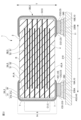
- 1 is a schematic perspective view of a chip-type electronic component 1 according to an embodiment.
- 2 is a partial cross-sectional view of the chip-type electronic component 1 taken along line II-II in FIG. 3 is a cross-sectional view of the chip-type electronic component 1 taken along line III-III in FIG. 1 is a diagram showing the second spacer main surface AS2 of the spacer 10 facing upward.
- 1 is a flowchart illustrating a manufacturing method of the chip-type electronic component 1.
- 2 is a modified partial cross-sectional view of the chip-type electronic component 1.
- Fig. 1 is a schematic perspective view of a chip-type electronic component 1 according to an embodiment.
- Fig. 2 is a partial cross-sectional view of the chip-type electronic component 1 taken along line II-II in Fig. 1.
- Fig. 3 is a cross-sectional view of the chip-type electronic component 1 taken along line III-III in Fig. 1.
- Figs. 1, 2, and 3 show the chip-type electronic component 1 bonded onto a mounting substrate 210.
- the chip-type electronic component 1 comprises a laminated ceramic capacitor 1A having a laminate 2 of a substantially rectangular parallelepiped shape and a pair of external electrodes 3 provided on both ends of the laminate 2, and a spacer 10 attached to the laminated ceramic capacitor 1A.
- the laminate 2 also includes an inner layer 6 including multiple pairs of dielectric layers 4 and internal electrode layers 5.
- the direction in which the pair of external electrodes 3 are provided is referred to as the length direction L
- the direction in which the dielectric layers 4 and the internal electrode layers 5 are stacked is referred to as the stacking direction T.
- the direction that intersects both the length direction L and the stacking direction T is referred to as the width direction W. Note that in this embodiment, the width direction W is perpendicular to both the length direction L and the stacking direction T.
- a pair of outer surfaces facing each other in the stacking direction T are the first capacitor main surface A1 and the second capacitor main surface A2
- a pair of outer surfaces facing each other in the width direction W are the first capacitor side surface B1 and the second capacitor side surface B2
- a pair of outer surfaces facing each other in the length direction L are the first capacitor end surface C1 and the second capacitor end surface C2.
- first capacitor main surface A1 and the second capacitor main surface A2 when there is no need to distinguish between the first capacitor main surface A1 and the second capacitor main surface A2, they will be collectively referred to as the capacitor main surface A, when there is no need to distinguish between the first capacitor side surface B1 and the second capacitor side surface B2, they will be collectively referred to as the capacitor side surface B, and when there is no need to distinguish between the first capacitor end surface C1 and the second capacitor end surface C2, they will be collectively referred to as the capacitor end surface C.
- the laminate 2 includes an inner layer portion 6, an outer layer portion 7 disposed on the capacitor main surface A side of the inner layer portion 6, and a side gap portion 8.
- the laminate 2 preferably has rounded ridge portions R.
- the ridge portions R are portions where two surfaces of the laminate 2, i.e., the capacitor main surface A and the capacitor side surface B, the capacitor main surface A and the capacitor end surface C, or the capacitor side surface B and the capacitor end surface C, intersect, and also include corners where the capacitor main surface A, the capacitor side surface B, and the capacitor end surface C intersect.
- the inner layer portion 6 includes a plurality of pairs of dielectric layers 4 and internal electrode layers 5 alternately stacked along the stacking direction T.
- the dielectric layer 4 is made of a ceramic material.
- a dielectric ceramic containing BaTiO3 as a main component is used as the ceramic material.
- the ceramic material may be one containing at least one of a Mn compound, an Fe compound, a Cr compound, a Co compound, a Nickel compound, or the like, added to the main component.
- the internal electrode layers 5 are preferably made of a metal material typified by, for example, nickel, Cu, Ag, Pd, an Ag-Pd alloy, Au, and the like.
- the internal electrode layer 5 comprises a plurality of first internal electrode layers 5A and a plurality of second internal electrode layers 5B.
- the first internal electrode layers 5A and the second internal electrode layers 5B are arranged alternately. Note that, when there is no need to distinguish between the first internal electrode layers 5A and the second internal electrode layers 5B, they will be collectively referred to as the internal electrode layer 5.
- the internal electrode layer 5 has opposing portions 52 that face each other between the first internal electrode layer 5A and the second internal electrode layer 5B, and lead-out portions 51 that do not face each other between the first internal electrode layer 5A and the second internal electrode layer 5B and are drawn out from the opposing portions 52 to one of the capacitor end faces C.
- the ends of the lead-out portions 51 are exposed to the capacitor end face C and are electrically connected to the external electrode 3.
- the extending directions of the lead-out portions 51 differ between the first internal electrode layer 5A and the second internal electrode layer 5B, and the lead-out portions 51 are drawn out alternately to the first capacitor end face C1 side and the second capacitor end face C2 side.
- An electric charge is accumulated between the opposing portions 52 of the first internal electrode layer 5A and the second internal electrode layer 5B that are adjacent to each other in the stacking direction T, and function as a capacitor.
- outer layer 7 The outer layer portions 7 are disposed on both capacitor main surface A sides of the inner layer portion 6 , and are made of the same material as the dielectric layers 4 of the inner layer portions 6 .
- the side gaps 8 are provided on both capacitor side surfaces B of the inner layer portion 6 in the laminate 2.
- the side gaps 8 are integrally manufactured from the same material as the dielectric layers 4.
- the external electrodes 3 are provided on both capacitor end faces C of the laminate 2. That is, a first external electrode 3A is formed on the first capacitor end face C1, and a second external electrode 3B is formed on the second capacitor end face C2.
- the external electrodes 3 cover not only the capacitor end face C, but also a portion of the capacitor main face A and the capacitor side face B on the capacitor end face C side.
- the external electrodes 3 include a base electrode layer 30 and a plating layer 31 formed on the outer periphery of the base electrode layer 30.
- the base electrode layer 30 is electrically connected to the end of the lead portion 51 of the internal electrode layer 5 exposed on the capacitor end surface C.
- the base electrode layer 30 is a so-called baked electrode obtained by baking a conductive paste containing a conductive metal such as copper, nickel, silver, palladium, a silver-palladium alloy, or gold, and the baked electrode contains a glass component and a metal.
- the glass component contains at least one selected from B, Si, Ba, Mg, Al, Li, and the like.
- the baked electrode is obtained by applying a conductive paste containing glass and a metal to the laminate 2 and baking it, and may be baked simultaneously with the internal electrode layer 5 and the dielectric layer 4, or may be baked after the internal electrode layer 5 is baked.
- a dielectric material instead of the glass component to form the baked electrode.
- the plating layer 31 includes a Ni plating layer 31a disposed around the outer periphery of the base electrode layer 30 so as to cover the base electrode layer 30, and a Sn plating layer 31b disposed around the outer periphery of the Ni plating layer 31a so as to cover the Ni plating layer 31a.
- the Ni plating layer 31a can prevent the base electrode layer 30 from being eroded by solder when mounting a ceramic electronic component, and the Sn plating layer 31b improves the wettability of the solder when mounting the multilayer ceramic capacitor 1A, allowing easy mounting.
- the Ni plating layer 31a is made of nickel or a plating of an alloy containing nickel.
- the Sn plating layer 31b is made of Sn or a plating of an alloy containing Sn.
- the plating layer 31 may contain at least one selected from, for example, Cu, Ni, Sn, Ag, Pd, an Ag-Pd alloy, Au, and the like.
- the spacer 10 includes a pair of two spacers, a first spacer 10A and a second spacer 10B.
- the first spacer 10A is disposed on one side of the second capacitor main surface A2 of the multilayer ceramic capacitor 1A in the length direction L, and the second spacer 10B is disposed on the other side.
- the first spacer 10A and the second spacer 10B have the same shape of a substantially rectangular shape, face each other, and are disposed at a certain distance apart.
- the spacer 10 is a roughly rectangular parallelepiped, and of the six outer surfaces, a pair of outer surfaces that face each other in the stacking direction T are the first spacer main surface AS1 and the second spacer main surface AS2, a pair of outer surfaces that face each other in the width direction W are the first spacer side surface BS1 and the second spacer side surface BS2, and a pair of outer surfaces that face each other in the length direction L are the first spacer end surface CS1 and the second spacer end surface CS2.
- the first spacer main surface AS 1 is the surface on the laminate 2 side
- the second spacer main surface AS 2 is the mounting surface to be mounted on the mounting substrate 210 .
- the first spacer main surface AS1 of the first spacer 10A contacts the second capacitor main surface A2 side of the first external electrode formed on the first capacitor end surface C1
- the first spacer main surface AS1 of the second spacer 10B contacts the second capacitor main surface A2 side of the first external electrode formed on the second capacitor end surface C2.
- the cross-sectional shape of the spacer 10 perpendicular to the stacking direction T is a rectangle whose short sides extend in the length direction L and whose long sides extend in the width direction W.
- the first spacer side surface BS1 and the second spacer side surface BS2 are surfaces along the short sides of the spacer 10
- the first spacer end surface CS1 and the second spacer end surface CS2 are surfaces along the short sides of the spacer 10.
- the first spacer end face CS1 of the first spacer 10A is formed on the first capacitor end face C1 side of the first external electrode 3A
- the second spacer end face CS2 of the second spacer 10B is formed on the second capacitor end face C2 side of the second external electrode 3B.
- first spacer main surface AS1 and the second spacer main surface AS2 when there is no need to distinguish between the first spacer main surface AS1 and the second spacer main surface AS2, they will be collectively referred to as the spacer main surface AS, when there is no need to distinguish between the first spacer side surface BS1 and the second spacer side surface BS2, they will be collectively referred to as the spacer side surface BS, and when there is no need to distinguish between the first spacer end surface CS1 and the second spacer end surface CS2, they will be collectively referred to as the spacer end surface CS.
- the spacer 10 is not limited to a rectangular parallelepiped shape, and may be another hexahedral shape in which the first spacer main surface AS1 has a larger area than the second spacer main surface AS2. Furthermore, the spacer side surface BS and the spacer end surface CS do not have to be arranged perpendicular to the second spacer main surface AS2, which is the mounting surface. Furthermore, for example, the first spacer side surface BS1, the second spacer side surface BS2, the first spacer end surface CS1, and the second spacer end surface CS2, etc. may be curved surfaces.
- the spacer 10 is made of so-called high-temperature solder, whose main component is an intermetallic compound containing a high melting point metal and a low melting point metal.
- main component means that the content is 50% or more.
- the high melting point metal includes at least one of Cu and Ni
- the low melting point metal includes Sn.
- the main component is an intermetallic compound including a high melting point metal including at least one of Cu and Ni, and a low melting point metal including Sn
- the intermetallic compound it has a melting point that does not melt even at the soldering temperature, and it is possible to arrange it while maintaining the desired shape even during soldering.
- the intermetallic compound it is particularly preferable for the intermetallic compound to be an intermetallic compound generated by the reaction of Sn with a Cu-Ni alloy.
- the high melting point metal that constitutes the intermetallic compound may further include Ag.
- the spacer 10 may be made of a conductive resin.
- the conductive resin contains a metal and a thermosetting resin.
- the spacer 10 is more flexible than a conductive layer made of, for example, a plating film or a sintered product of a conductive paste, because the spacer 10 contains resin.
- the metal contained in the conductive resin can be Ag, Cu, or an alloy thereof. Also, a metal powder with Ag coating on the surface can be used. When using a metal powder with Ag coating on the surface, it is preferable to use Cu or Ni as the metal powder. Also, Cu with an oxidation prevention treatment can be used.
- the metal contained in the conductive resin is preferably contained in an amount of 35 vol% or more and 75 vol% or less with respect to the total volume of the conductive resin.
- the metal contained in the conductive resin can be spherical, flat, or the like, but it is preferable to use a mixture of spherical metal powder and flat metal powder.
- the average particle size of the metal contained in the conductive resin is not particularly limited.
- the average particle size of the conductive filler may be, for example, about 0.3 ⁇ m or more and 10 ⁇ m or less.
- the metal contained in the conductive resin mainly carries out the electrical conductivity of the conductive resin. Specifically, the conductive fillers come into contact with each other to form an electrical path inside the conductive resin.
- thermosetting resins such as epoxy resin, phenol resin, urethane resin, silicone resin, polyimide resin, etc.
- epoxy resin which has excellent heat resistance, moisture resistance, adhesion, etc.
- the resin contained in the conductive resin is preferably contained in an amount of 25 vol% or more and 65 vol% or less with respect to the total volume of the conductive resin.
- the conductive resin preferably contains a curing agent together with the thermosetting resin.
- the curing agent when an epoxy resin is used as the base resin, various known compounds such as phenol-based, amine-based, acid anhydride-based, and imidazole-based compounds can be used as the curing agent for the epoxy resin.
- the spacer 10 has recesses 11 formed on the surface of the second spacer main surface AS2, which is the mounting surface. A plurality of recesses 11 are formed.
- Fig. 4 is a view of the spacer 10 with the second spacer main surface AS2 facing up. According to this embodiment, by forming the recesses 11 on the surface on the second spacer main surface AS2 side, when the chip-type electronic component 1 is mounted on the mounting board 210, the solder 240 enters the recesses 11, and the fixing strength between the solder 240 and the spacer 10 can be improved by the anchor effect.
- the total opening area of the recesses 11 is preferably 25% or more and 75% or less of the surface area of the second spacer main surface AS2. The reason is that if the total opening area of the recesses 11 is greater than 75% of the area of the second spacer main surface AS2, much of the solder 240 is trapped in the recesses 11, making it difficult for the solder 240 to reach the spacer end surface CS and spacer side surface BS of the spacer 10, weakening the bonding strength between the spacer 10 and the mounting substrate 210.
- the total opening area of the recesses 11 is less than 25% of the entire area of the second spacer main surface AS2, the bonding area between the solder 240 and the spacer 10 is reduced, and therefore the anchor effect with the solder 240 cannot be obtained sufficiently.
- the total opening area of the recesses 11 of the spacer 10 is the sum of the areas of the openings of the recesses 11 when viewed from the second spacer main surface AS2 side.
- the second spacer main surface AS2 of the spacer 10 is not flat but has projections and recesses.
- the distance in the stacking direction T between the most protruding position on the second spacer main surface AS2 of the spacer 10, i.e., the top of the convex portion, and the first spacer main surface AS1 is defined as the thickness of the spacer 10. If the second spacer main surface AS2 is abutted against a flat surface, the flat surface abuts against the top of the convex portion of the second spacer main surface AS2.
- the portion within 1% of the thickness of the spacer 10 from the position of this flat surface, i.e., the top of the convex portion, toward the first spacer main surface AS1 is considered to be included in the flat surface of the second spacer main surface AS2, and the portion recessed by more than 1% of the thickness of the spacer 10 is defined as the recess 11.
- the opening area of one recess 11 is preferably 0.1% to 70% of the surface area of the second spacer main surface AS2. The reason is that if the opening area of one recess 11 is larger than 70% of the area of the second spacer main surface AS2, too much solder 240 is trapped in the recess 11, making it difficult for the solder 240 to reach the spacer end surface CS and spacer side surface BS of the spacer 10, which may reduce the bonding strength between the spacer 10 and the mounting substrate 210.
- the opening area of one recess 11 is smaller than 0.1% of the area of the second spacer main surface AS2, the solder 240 will not sufficiently enter the recess 11 of the spacer 10, and therefore will not be able to fully benefit from the anchor effect. Furthermore, the opening area of one recess 11 is more preferably 0.5% or more and 65% or less of the area of the second spacer main surface AS2, even more preferably 1% or more and 60% or less, and particularly preferably 5% or more and 50% or less.
- the number of recesses 11 is appropriately selected so as to satisfy the above conditions of the total opening area of the recesses 11 and the opening area of one recess 11 .
- Internal shape of recess 11 There is no particular limitation on the shape of the inside of the recess 11. For example, it may be a tapered shape that becomes narrower from the second spacer main surface AS2 toward the first spacer main surface AS1, or it may be an octopus pot shape in which the inside is larger than the opening.
- the depth of the recess 11 is preferably 1% to 50% of the thickness of the spacer 10 in the stacking direction T.
- the stacking direction T is the direction in which the dielectric layers 4 and the internal electrode layers 5 are stacked in the multilayer ceramic capacitor 1A described above, and in the case of the spacer 10, is the direction connecting the first spacer main surface AS1 and the second spacer main surface AS2.
- the "depth” refers to the length in the stacking direction T from the opening to the bottom of the recess 11.
- the depth of the recess 11 is preferably 1% or more of the thickness of the spacer 10 in the stacking direction T is that if the depth of the recess 11 is less than 1%, the surface will be smooth and it will be difficult to obtain the anchor effect described below.
- the depth of the recess 11 is 50% or less of the thickness of the spacer 10 in the stacking direction T is that if the depth of the recess 11 is greater than 50%, the length of the portion of the spacer 10 where the recess 11 is provided in the stacking direction T will be shortened, which may result in a decrease in the mechanical strength of the spacer 10.
- the recesses 11 are a mixture of recesses 11 of 1% or more and less than 5% and recesses 11 of 5% or more. Furthermore, the average depth of the recesses 11 of 5% or more is more preferably 5% or more and 35% or less, and even more preferably 10% or more and 20% or less, of the thickness of the spacer 10 in the stacking direction T. It is preferable that the recesses 11 are a mixture of recesses 11 of 1% or more and less than 5% and recesses 11 of 5% or more. The recesses 11 may be only recesses 11 of 1% or more and less than 5% or only recesses 11 of 5% or more.
- recesses 11 are formed also on the surfaces of two spacer end faces CS of the spacer 10 that face each other in the length direction L. It is also preferable that recesses 11 are formed also on the surfaces of two spacer side faces BS of the spacer 10 that face each other in the width direction W. In this way, when recesses 11 are arranged on the surface of the spacer end face CS and the surface of the spacer side face BS, the solder 240 wets onto the surface of the spacer end face CS and the spacer side face BS, thereby improving the adhesion between the solder 240 and the external electrode 3.
- the recesses 11 of the spacer 10 are provided on the second spacer main surface AS2, they do not have to be provided on other surfaces. Also, if they are provided on other surfaces, they may be located on some of the surfaces, not all of the surfaces.
- the “some surfaces” may be any surfaces.
- the recess 11 is provided on the second spacer main surface AS2, it may be arranged on both or one of the spacer side surfaces BS, or on both or one of the spacer end surfaces CS.
- the recess 11 is disposed on one side, it is more preferable that the recess 11 is formed on the end face CS1 of the first spacer 10A and the end face CS2 of the second spacer 10B.
- the solder 240 that wets and rises on the first spacer end face CS1 and the second spacer end face CS2 is absorbed by the recess 11 on the end face CS1 of the first spacer 10A and the recess 11 on the end face CS2 of the second spacer 10B, so that excessive fillet formation can be suppressed.
- the recess 11 of the spacer 10 may be disposed on different faces in the first spacer 10A and the second spacer 10B, so long as it is provided on the second spacer main surface AS2.
- a land 230 is arranged on a mounting substrate 210 on which the chip-type electronic component 1 is mounted.
- the land 230 has a first land 230A and a second land 230B.
- the first spacer 10A is connected to the first land 230A
- the second spacer 10B is connected to the second land 230B by solder 240, respectively.
- a recess 11 is formed on the surface on the second spacer main surface AS2 side, and solder 240 fills this recess 11. Therefore, the chip-type electronic component 1 and the mounting substrate 210 are bonded with high adhesion strength due to the anchor effect.
- the manufacturing process of the chip-type electronic component 1 includes a laminate manufacturing step S1, an external electrode forming step S2, a spacer arranging step S3, and a recess forming step S4.
- a material sheet is prepared in which a pattern of the internal electrode layer 5 is printed with a conductive paste on a ceramic green sheet for lamination, which is formed by forming a ceramic slurry into a sheet shape. Then, a plurality of material sheets are stacked so that the internal electrode patterns are shifted by half a pitch between adjacent material sheets in the longitudinal direction. Furthermore, outer layer ceramic green sheets that will become the outer layer parts are stacked on both sides of the plurality of stacked material sheets, and are thermocompression-bonded to form a mother block member. A plurality of laminates 2 are manufactured by dividing the mother block member along a cutting line corresponding to the dimensions of the laminate.
- a base electrode layer 30 is formed by, for example, applying a conductive paste containing a conductive metal and glass to both ends of the laminate 2 and baking it. As shown in Fig. 2, the base electrode layer 30 is formed so as to cover not only the capacitor end faces C on both sides of the laminate 2 but also extend to the capacitor main surface A side and cover a part of the capacitor main surface A on the capacitor end face C side.
- a Ni plating layer 31a is first formed on the outer periphery of the base electrode layer 30 so as to cover the base electrode layer 30.
- a Sn plating layer 31b is formed on the outer periphery of the Ni plating layer 31a so as to cover the Ni plating layer 31a.
- a multilayer ceramic capacitor 1A in which the external electrodes 3 are formed on the laminate 2 is manufactured.
- Spacer placement step S3 In the spacer arranging step S3, an intermetallic compound paste, which is the material of the spacer 10, is arranged on the outer periphery of the external electrode 3 on the second capacitor main surface A2 side of the multilayer ceramic capacitor 1A.
- the intermetallic compound paste is a so-called high temperature solder containing, as a main component, an intermetallic compound containing at least one of Cu and Ni as a high melting point metal and Sn as a low melting point metal.
- Such an intermetallic compound paste is once melted at 200° C. or higher and then placed in a liquid state on the surface of the Sn plating layer 31b.
- High temperature solder has a melting point that does not melt even at ordinary soldering temperatures, and it is possible to arrange the solder while maintaining the desired shape.
- the intermetallic compound paste is bonded to, for example, an alumina plate, which has a desired unevenness and is not to be bonded to the high-temperature solder, from the second main surface side.
- the alumina plate is removed. This allows the recess 11 to be formed on the second spacer main surface AS2 of the spacer 10.
- the recesses 11 on the spacer end faces CS and the spacer side faces BS can be formed by, for example, arranging an alumina plate so as to wrap around the end faces and the side faces.
- a method of abutting an alumina plate is preferable.
- a method of forming the recess 11 by sandblasting or the like is preferable.
- either method may be used to form the recess 11.
- the method for forming the recesses 11 is not limited to this, and other methods may be used.
- the recesses may be formed by roughening the hardened surface with, for example, a file, or by a chemical method such as etching. Through the above steps, the chip-type electronic component 1 is manufactured.
- the recess 11 is formed on the surface on the second spacer main surface AS2 side, so that when the chip-type electronic component 1 is mounted on the mounting substrate 210, the solder 240 enters the recess 11, and the anchor effect improves the adhesive strength between the solder 240 and the spacer 10.
- the solder 240 may not only be disposed between the spacer 10 and the land 230 as shown in FIG. 2, but may also cover the spacer 10 and the side of the external electrode 3 as shown in FIG. 6.
- the spacer 10 of the embodiment has recesses 11 formed on the surfaces of the spacer end faces CS and the spacer side faces BS. Therefore, when the solder 240 covers the spacer 10 and the side of the external electrode 3 as shown in FIG. 6, the solder 240 penetrates into the surface recesses 11 on the surfaces of the spacer end faces CS and the spacer side faces BS, and the stronger anchor effect can further improve the adhesive strength between the solder 240 and the spacer 10.
- a chip-type electronic component comprising: a laminate including a plurality of internal electrode layers and a plurality of internal dielectric layers arranged alternately with each other; a multilayer ceramic capacitor including external electrodes provided on each of the capacitor end faces, when two faces of the laminate opposing each other in a stacking direction are defined as capacitor main faces, two faces opposing each other in a width direction intersecting the stacking direction are defined as capacitor side faces, and two faces opposing each other in a length direction intersecting the stacking direction and the width direction are defined as capacitor end faces; and a spacer arranged on both sides in the length direction of the capacitor main face on a mounting substrate side of the multilayer ceramic capacitor, wherein a recess is formed on a surface of the spacer main face on the mounting substrate side when the two faces of the spacer opposing each other in the stacking direction are defined as spacer main faces.
- ⁇ 2> The chip-type electronic component described in ⁇ 1>, in which the spacer is mainly composed of an intermetallic compound containing a high melting point metal and a low melting point metal.
- ⁇ 3> The chip-type electronic component described in ⁇ 2>, in which the high melting point metal includes at least one of Cu and Ni, and the low melting point metal includes Sn.
- ⁇ 5> A chip-type electronic component according to any one of ⁇ 1> to ⁇ 4>, in which the total opening area of the recesses of the spacer is 25% to 75% of the surface area of the main surface of the spacer on the mounting substrate side.
- ⁇ 6> A chip-type electronic component according to any one of ⁇ 1> to ⁇ 5>, in which the opening area of one of the recesses of the spacer is 0.1% to 70% of the surface area of the main surface of the spacer on the mounting substrate side.
- ⁇ 7> A chip-type electronic component according to any one of ⁇ 1> to ⁇ 6>, in which the depth of the recess in the stacking direction is 1% to 50% of the thickness of the spacer in the stacking direction.
- ⁇ 8> A chip-type electronic component according to any one of ⁇ 1> to ⁇ 7>, in which the spacer has recesses formed on the surfaces of two spacer end faces CS that face each other in the longitudinal direction.
- a chip-type electronic component according to any one of ⁇ 1> to ⁇ 8>, in which the spacer has recesses formed on the surfaces of two spacer side surfaces that face each other in the width direction.
- the chip-type electronic component according to any one of ⁇ 1> to ⁇ 9>, in which one of the two capacitor end faces in the laminate is a first capacitor end face and the other is a second capacitor end face, the face of the two capacitor main faces facing the spacer is a second capacitor main face, and in each of the spacers, when the one of the two spacer end faces facing each other in the length direction is a first spacer end face and the other is a second spacer end face, the spacer has a first spacer that contacts a portion of the first external electrode arranged on the side of the first capacitor end face that extends toward the second capacitor main face, and a second spacer that contacts a portion of the second external electrode arranged on the side of the second capacitor end face that extends toward the second capacitor main face, and a recess is formed in the first spacer end face, which is the face of the first spacer that faces the first capacitor end face, and a recess is formed in the second spacer end face, which is the face of the second spacer that faces
Landscapes
- Engineering & Computer Science (AREA)
- Microelectronics & Electronic Packaging (AREA)
- Power Engineering (AREA)
- Physics & Mathematics (AREA)
- Electromagnetism (AREA)
- Manufacturing & Machinery (AREA)
- Ceramic Engineering (AREA)
- Fixed Capacitors And Capacitor Manufacturing Machines (AREA)
- Ceramic Capacitors (AREA)
Abstract
L'invention fournit un composant électronique de type puce qui est moins susceptible de provoquer la séparation d'un espaceur et d'un substrat de montage. Un composant électronique de type puce 1 de la présente invention comprend un condensateur céramique multicouche 1A et des espaceurs 10. Le condensateur céramique multicouche 1A comprend : un empilement 2 qui comprend des couches d'électrode interne 5 et des couches diélectriques 4 qui sont disposées en alternance ; et des électrodes externes 3. Lorsque les deux surfaces de l'empilement 2 opposées l'une à l'autre dans la direction multicouche sont des surfaces principales de condensateur A, leurs deux surfaces opposées l'une à l'autre dans la direction de la largeur sont des surfaces latérales de condensateur B, et leurs deux surfaces opposées l'une à l'autre dans la direction de la longueur sont des surfaces d'extrémité de condensateur C, les électrodes externes 3 sont respectivement disposées sur les surfaces d'extrémité de condensateur C. Les espaceurs 10 sont disposés des deux côtés dans la direction de la longueur de la surface principale de condensateur A sur le côté substrat de montage du condensateur céramique multicouche 1A. Lorsque les deux surfaces opposées l'une à l'autre dans la direction multicouche de chacun des espaceurs 10 sont des surfaces principales d'espacement AS, un évidement 11 est formé dans la surface de la surface principale d'élément d'espacement AS sur le côté substrat de montage.
Applications Claiming Priority (2)
| Application Number | Priority Date | Filing Date | Title |
|---|---|---|---|
| JP2022159642 | 2022-10-03 | ||
| JP2022-159642 | 2022-10-03 |
Publications (1)
| Publication Number | Publication Date |
|---|---|
| WO2024075404A1 true WO2024075404A1 (fr) | 2024-04-11 |
Family
ID=90607944
Family Applications (1)
| Application Number | Title | Priority Date | Filing Date |
|---|---|---|---|
| PCT/JP2023/029583 WO2024075404A1 (fr) | 2022-10-03 | 2023-08-16 | Composant électronique de type puce |
Country Status (1)
| Country | Link |
|---|---|
| WO (1) | WO2024075404A1 (fr) |
Citations (5)
| Publication number | Priority date | Publication date | Assignee | Title |
|---|---|---|---|---|
| JPH0969401A (ja) * | 1995-08-31 | 1997-03-11 | Oki Electric Ind Co Ltd | 表面実装部品 |
| JP2007081004A (ja) * | 2005-09-13 | 2007-03-29 | Matsushita Electric Ind Co Ltd | 電子部品 |
| WO2018101405A1 (fr) * | 2016-12-01 | 2018-06-07 | 株式会社村田製作所 | Composant électronique de type puce |
| JP2018190952A (ja) * | 2017-05-04 | 2018-11-29 | サムソン エレクトロ−メカニックス カンパニーリミテッド. | 積層型電子部品及びその実装基板 |
| JP2022099069A (ja) * | 2020-12-22 | 2022-07-04 | 株式会社村田製作所 | 積層セラミックコンデンサ及び積層セラミックコンデンサの製造方法 |
-
2023
- 2023-08-16 WO PCT/JP2023/029583 patent/WO2024075404A1/fr unknown
Patent Citations (5)
| Publication number | Priority date | Publication date | Assignee | Title |
|---|---|---|---|---|
| JPH0969401A (ja) * | 1995-08-31 | 1997-03-11 | Oki Electric Ind Co Ltd | 表面実装部品 |
| JP2007081004A (ja) * | 2005-09-13 | 2007-03-29 | Matsushita Electric Ind Co Ltd | 電子部品 |
| WO2018101405A1 (fr) * | 2016-12-01 | 2018-06-07 | 株式会社村田製作所 | Composant électronique de type puce |
| JP2018190952A (ja) * | 2017-05-04 | 2018-11-29 | サムソン エレクトロ−メカニックス カンパニーリミテッド. | 積層型電子部品及びその実装基板 |
| JP2022099069A (ja) * | 2020-12-22 | 2022-07-04 | 株式会社村田製作所 | 積層セラミックコンデンサ及び積層セラミックコンデンサの製造方法 |
Similar Documents
| Publication | Publication Date | Title |
|---|---|---|
| JP2019009359A (ja) | 積層セラミック電子部品及びその実装構造 | |
| JP7444048B2 (ja) | 積層セラミックコンデンサ及び積層セラミックコンデンサの製造方法 | |
| US11657977B2 (en) | Method of manufacturing multilayer ceramic capacitor | |
| US11735370B2 (en) | Multilayer ceramic capacitor | |
| US11749461B2 (en) | Multilayer ceramic capacitor | |
| CN113555215B (zh) | 层叠陶瓷电容器 | |
| US11670458B2 (en) | Multilayer ceramic capacitor | |
| CN109859948B (zh) | 陶瓷电子部件 | |
| US20220108841A1 (en) | Multilayer ceramic capacitor | |
| US10573459B2 (en) | Multilayer ceramic electronic component and mounting structure thereof | |
| KR20210130649A (ko) | 적층 세라믹 콘덴서 | |
| JP6696121B2 (ja) | 複合電子部品および抵抗素子 | |
| US11705284B2 (en) | Multilayer ceramic capacitor | |
| US11756735B2 (en) | Multilayer ceramic capacitor | |
| CN113555220B (zh) | 层叠陶瓷电容器 | |
| US20220108843A1 (en) | Multilayer ceramic capacitor | |
| WO2024075404A1 (fr) | Composant électronique de type puce | |
| CN113555221B (zh) | 层叠陶瓷电容器 | |
| CN113555219B (zh) | 层叠陶瓷电容器 | |
| JP2022177518A (ja) | 積層セラミックコンデンサ | |
| JP2000106322A (ja) | 積層セラミックコンデンサ | |
| CN113555218A (zh) | 层叠陶瓷电容器 | |
| WO2023085263A1 (fr) | Condensateur céramique multicouche et pâte de fabrication de bosse | |
| WO2023085265A1 (fr) | Condensateur céramique stratifié et pâte pour la fabrication de bosses | |
| US20230298814A1 (en) | Mounting structure and mounting method of electronic component |
Legal Events
| Date | Code | Title | Description |
|---|---|---|---|
| 121 | Ep: the epo has been informed by wipo that ep was designated in this application |
Ref document number: 23874537 Country of ref document: EP Kind code of ref document: A1 |