WO2024075404A1 - Chip-type electronic component - Google Patents
Chip-type electronic component Download PDFInfo
- Publication number
- WO2024075404A1 WO2024075404A1 PCT/JP2023/029583 JP2023029583W WO2024075404A1 WO 2024075404 A1 WO2024075404 A1 WO 2024075404A1 JP 2023029583 W JP2023029583 W JP 2023029583W WO 2024075404 A1 WO2024075404 A1 WO 2024075404A1
- Authority
- WO
- WIPO (PCT)
- Prior art keywords
- spacer
- capacitor
- face
- chip
- type electronic
- Prior art date
Links
- 125000006850 spacer group Chemical group 0.000 claims abstract description 236
- 239000003990 capacitor Substances 0.000 claims abstract description 97
- 239000000758 substrate Substances 0.000 claims abstract description 23
- 239000003985 ceramic capacitor Substances 0.000 claims abstract description 21
- 229910052751 metal Inorganic materials 0.000 claims description 34
- 239000002184 metal Substances 0.000 claims description 34
- 229920005989 resin Polymers 0.000 claims description 28
- 239000011347 resin Substances 0.000 claims description 28
- 238000002844 melting Methods 0.000 claims description 19
- 230000008018 melting Effects 0.000 claims description 19
- 229910000765 intermetallic Inorganic materials 0.000 claims description 15
- 229910052759 nickel Inorganic materials 0.000 claims description 11
- 229910052802 copper Inorganic materials 0.000 claims description 10
- 238000003475 lamination Methods 0.000 claims description 7
- 238000000926 separation method Methods 0.000 abstract 1
- 229910000679 solder Inorganic materials 0.000 description 29
- PXHVJJICTQNCMI-UHFFFAOYSA-N Nickel Chemical compound [Ni] PXHVJJICTQNCMI-UHFFFAOYSA-N 0.000 description 22
- 238000007747 plating Methods 0.000 description 20
- 239000010949 copper Substances 0.000 description 10
- 238000000034 method Methods 0.000 description 8
- 230000000694 effects Effects 0.000 description 7
- 238000004519 manufacturing process Methods 0.000 description 7
- 239000000463 material Substances 0.000 description 7
- 150000001875 compounds Chemical class 0.000 description 6
- PNEYBMLMFCGWSK-UHFFFAOYSA-N aluminium oxide Inorganic materials [O-2].[O-2].[O-2].[Al+3].[Al+3] PNEYBMLMFCGWSK-UHFFFAOYSA-N 0.000 description 5
- 239000000919 ceramic Substances 0.000 description 5
- 239000011521 glass Substances 0.000 description 5
- 239000000843 powder Substances 0.000 description 5
- 229910045601 alloy Inorganic materials 0.000 description 4
- 239000000956 alloy Substances 0.000 description 4
- 239000003822 epoxy resin Substances 0.000 description 4
- KDLHZDBZIXYQEI-UHFFFAOYSA-N palladium Substances [Pd] KDLHZDBZIXYQEI-UHFFFAOYSA-N 0.000 description 4
- 229920000647 polyepoxide Polymers 0.000 description 4
- 229910052709 silver Inorganic materials 0.000 description 4
- 229910001252 Pd alloy Inorganic materials 0.000 description 3
- 230000015572 biosynthetic process Effects 0.000 description 3
- 229910010293 ceramic material Inorganic materials 0.000 description 3
- 239000003795 chemical substances by application Substances 0.000 description 3
- 239000010931 gold Substances 0.000 description 3
- RAXXELZNTBOGNW-UHFFFAOYSA-N imidazole Natural products C1=CNC=N1 RAXXELZNTBOGNW-UHFFFAOYSA-N 0.000 description 3
- 239000000203 mixture Substances 0.000 description 3
- 229910052763 palladium Inorganic materials 0.000 description 3
- 238000005476 soldering Methods 0.000 description 3
- 229920001187 thermosetting polymer Polymers 0.000 description 3
- 239000000853 adhesive Substances 0.000 description 2
- 230000001070 adhesive effect Effects 0.000 description 2
- 239000011248 coating agent Substances 0.000 description 2
- 238000000576 coating method Methods 0.000 description 2
- 239000011231 conductive filler Substances 0.000 description 2
- 239000002245 particle Substances 0.000 description 2
- 239000010944 silver (metal) Substances 0.000 description 2
- RYGMFSIKBFXOCR-UHFFFAOYSA-N Copper Chemical compound [Cu] RYGMFSIKBFXOCR-UHFFFAOYSA-N 0.000 description 1
- 229910002482 Cu–Ni Inorganic materials 0.000 description 1
- 241000238413 Octopus Species 0.000 description 1
- ISWSIDIOOBJBQZ-UHFFFAOYSA-N Phenol Chemical compound OC1=CC=CC=C1 ISWSIDIOOBJBQZ-UHFFFAOYSA-N 0.000 description 1
- BQCADISMDOOEFD-UHFFFAOYSA-N Silver Chemical compound [Ag] BQCADISMDOOEFD-UHFFFAOYSA-N 0.000 description 1
- 150000008065 acid anhydrides Chemical class 0.000 description 1
- 150000001412 amines Chemical class 0.000 description 1
- 229910002113 barium titanate Inorganic materials 0.000 description 1
- 238000006243 chemical reaction Methods 0.000 description 1
- 238000005520 cutting process Methods 0.000 description 1
- 238000010586 diagram Methods 0.000 description 1
- 239000003989 dielectric material Substances 0.000 description 1
- 238000005530 etching Methods 0.000 description 1
- PCHJSUWPFVWCPO-UHFFFAOYSA-N gold Chemical compound [Au] PCHJSUWPFVWCPO-UHFFFAOYSA-N 0.000 description 1
- 229910052737 gold Inorganic materials 0.000 description 1
- 239000007788 liquid Substances 0.000 description 1
- 239000007769 metal material Substances 0.000 description 1
- 150000002739 metals Chemical class 0.000 description 1
- 150000002816 nickel compounds Chemical class 0.000 description 1
- 230000003647 oxidation Effects 0.000 description 1
- 238000007254 oxidation reaction Methods 0.000 description 1
- SWELZOZIOHGSPA-UHFFFAOYSA-N palladium silver Chemical compound [Pd].[Ag] SWELZOZIOHGSPA-UHFFFAOYSA-N 0.000 description 1
- -1 phenol-based Chemical class 0.000 description 1
- 239000005011 phenolic resin Substances 0.000 description 1
- 230000010287 polarization Effects 0.000 description 1
- 229920001721 polyimide Polymers 0.000 description 1
- 239000009719 polyimide resin Substances 0.000 description 1
- 230000002265 prevention Effects 0.000 description 1
- 230000036632 reaction speed Effects 0.000 description 1
- 238000007788 roughening Methods 0.000 description 1
- 238000005488 sandblasting Methods 0.000 description 1
- 229920002050 silicone resin Polymers 0.000 description 1
- 239000004332 silver Substances 0.000 description 1
- 239000002002 slurry Substances 0.000 description 1
- 239000000126 substance Substances 0.000 description 1
- 229920002803 thermoplastic polyurethane Polymers 0.000 description 1
- 229910052718 tin Inorganic materials 0.000 description 1
- 239000011135 tin Substances 0.000 description 1
- 230000003313 weakening effect Effects 0.000 description 1
Images


Definitions
- the present invention relates to chip-type electronic components.
- a multilayer ceramic capacitor has a laminate having an inner layer in which dielectric layers and internal electrodes are alternately stacked, and external electrodes provided on both longitudinal end faces of the laminate.
- the dielectric layers are polarized, and the multilayer ceramic capacitor may vibrate in the polarization direction. This vibration may then be transmitted to the mounting board, potentially causing cracks in the mounting board.
- a spacer is placed on the mounting surface side of the multilayer ceramic capacitor to make it a chip-type electronic component, and the spacer cushions the vibration and suppresses the vibration transmitted to the mounting board (see Patent Document 1).
- the spacer may peel off from the mounting board.
- the objective of the present invention is to provide a chip-type electronic component in which the spacer is less likely to peel off from the mounting substrate.
- the present invention provides a chip-type electronic component comprising: a laminate including a plurality of internal electrode layers and a plurality of internal dielectric layers arranged alternately with each other; a multilayer ceramic capacitor including external electrodes provided on each of the capacitor end faces when two surfaces of the laminate opposing each other in the lamination direction are defined as capacitor main faces, two surfaces opposing each other in a width direction intersecting with the lamination direction are defined as capacitor side faces, and two surfaces opposing each other in a length direction intersecting with the lamination direction and the width direction are defined as capacitor end faces; and a spacer disposed on both sides in the length direction of the capacitor main face on the mounting substrate side of the multilayer ceramic capacitor, wherein a recess is formed on the surface of the spacer main face on the mounting substrate side when the two surfaces of the spacer opposing each other in the lamination direction are defined as spacer main faces.
- the present invention provides a chip-type electronic component in which the spacer is less likely to peel off from the mounting substrate.
- 1 is a schematic perspective view of a chip-type electronic component 1 according to an embodiment.
- 2 is a partial cross-sectional view of the chip-type electronic component 1 taken along line II-II in FIG. 3 is a cross-sectional view of the chip-type electronic component 1 taken along line III-III in FIG. 1 is a diagram showing the second spacer main surface AS2 of the spacer 10 facing upward.
- 1 is a flowchart illustrating a manufacturing method of the chip-type electronic component 1.
- 2 is a modified partial cross-sectional view of the chip-type electronic component 1.
- Fig. 1 is a schematic perspective view of a chip-type electronic component 1 according to an embodiment.
- Fig. 2 is a partial cross-sectional view of the chip-type electronic component 1 taken along line II-II in Fig. 1.
- Fig. 3 is a cross-sectional view of the chip-type electronic component 1 taken along line III-III in Fig. 1.
- Figs. 1, 2, and 3 show the chip-type electronic component 1 bonded onto a mounting substrate 210.
- the chip-type electronic component 1 comprises a laminated ceramic capacitor 1A having a laminate 2 of a substantially rectangular parallelepiped shape and a pair of external electrodes 3 provided on both ends of the laminate 2, and a spacer 10 attached to the laminated ceramic capacitor 1A.
- the laminate 2 also includes an inner layer 6 including multiple pairs of dielectric layers 4 and internal electrode layers 5.
- the direction in which the pair of external electrodes 3 are provided is referred to as the length direction L
- the direction in which the dielectric layers 4 and the internal electrode layers 5 are stacked is referred to as the stacking direction T.
- the direction that intersects both the length direction L and the stacking direction T is referred to as the width direction W. Note that in this embodiment, the width direction W is perpendicular to both the length direction L and the stacking direction T.
- a pair of outer surfaces facing each other in the stacking direction T are the first capacitor main surface A1 and the second capacitor main surface A2
- a pair of outer surfaces facing each other in the width direction W are the first capacitor side surface B1 and the second capacitor side surface B2
- a pair of outer surfaces facing each other in the length direction L are the first capacitor end surface C1 and the second capacitor end surface C2.
- first capacitor main surface A1 and the second capacitor main surface A2 when there is no need to distinguish between the first capacitor main surface A1 and the second capacitor main surface A2, they will be collectively referred to as the capacitor main surface A, when there is no need to distinguish between the first capacitor side surface B1 and the second capacitor side surface B2, they will be collectively referred to as the capacitor side surface B, and when there is no need to distinguish between the first capacitor end surface C1 and the second capacitor end surface C2, they will be collectively referred to as the capacitor end surface C.
- the laminate 2 includes an inner layer portion 6, an outer layer portion 7 disposed on the capacitor main surface A side of the inner layer portion 6, and a side gap portion 8.
- the laminate 2 preferably has rounded ridge portions R.
- the ridge portions R are portions where two surfaces of the laminate 2, i.e., the capacitor main surface A and the capacitor side surface B, the capacitor main surface A and the capacitor end surface C, or the capacitor side surface B and the capacitor end surface C, intersect, and also include corners where the capacitor main surface A, the capacitor side surface B, and the capacitor end surface C intersect.
- the inner layer portion 6 includes a plurality of pairs of dielectric layers 4 and internal electrode layers 5 alternately stacked along the stacking direction T.
- the dielectric layer 4 is made of a ceramic material.
- a dielectric ceramic containing BaTiO3 as a main component is used as the ceramic material.
- the ceramic material may be one containing at least one of a Mn compound, an Fe compound, a Cr compound, a Co compound, a Nickel compound, or the like, added to the main component.
- the internal electrode layers 5 are preferably made of a metal material typified by, for example, nickel, Cu, Ag, Pd, an Ag-Pd alloy, Au, and the like.
- the internal electrode layer 5 comprises a plurality of first internal electrode layers 5A and a plurality of second internal electrode layers 5B.
- the first internal electrode layers 5A and the second internal electrode layers 5B are arranged alternately. Note that, when there is no need to distinguish between the first internal electrode layers 5A and the second internal electrode layers 5B, they will be collectively referred to as the internal electrode layer 5.
- the internal electrode layer 5 has opposing portions 52 that face each other between the first internal electrode layer 5A and the second internal electrode layer 5B, and lead-out portions 51 that do not face each other between the first internal electrode layer 5A and the second internal electrode layer 5B and are drawn out from the opposing portions 52 to one of the capacitor end faces C.
- the ends of the lead-out portions 51 are exposed to the capacitor end face C and are electrically connected to the external electrode 3.
- the extending directions of the lead-out portions 51 differ between the first internal electrode layer 5A and the second internal electrode layer 5B, and the lead-out portions 51 are drawn out alternately to the first capacitor end face C1 side and the second capacitor end face C2 side.
- An electric charge is accumulated between the opposing portions 52 of the first internal electrode layer 5A and the second internal electrode layer 5B that are adjacent to each other in the stacking direction T, and function as a capacitor.
- outer layer 7 The outer layer portions 7 are disposed on both capacitor main surface A sides of the inner layer portion 6 , and are made of the same material as the dielectric layers 4 of the inner layer portions 6 .
- the side gaps 8 are provided on both capacitor side surfaces B of the inner layer portion 6 in the laminate 2.
- the side gaps 8 are integrally manufactured from the same material as the dielectric layers 4.
- the external electrodes 3 are provided on both capacitor end faces C of the laminate 2. That is, a first external electrode 3A is formed on the first capacitor end face C1, and a second external electrode 3B is formed on the second capacitor end face C2.
- the external electrodes 3 cover not only the capacitor end face C, but also a portion of the capacitor main face A and the capacitor side face B on the capacitor end face C side.
- the external electrodes 3 include a base electrode layer 30 and a plating layer 31 formed on the outer periphery of the base electrode layer 30.
- the base electrode layer 30 is electrically connected to the end of the lead portion 51 of the internal electrode layer 5 exposed on the capacitor end surface C.
- the base electrode layer 30 is a so-called baked electrode obtained by baking a conductive paste containing a conductive metal such as copper, nickel, silver, palladium, a silver-palladium alloy, or gold, and the baked electrode contains a glass component and a metal.
- the glass component contains at least one selected from B, Si, Ba, Mg, Al, Li, and the like.
- the baked electrode is obtained by applying a conductive paste containing glass and a metal to the laminate 2 and baking it, and may be baked simultaneously with the internal electrode layer 5 and the dielectric layer 4, or may be baked after the internal electrode layer 5 is baked.
- a dielectric material instead of the glass component to form the baked electrode.
- the plating layer 31 includes a Ni plating layer 31a disposed around the outer periphery of the base electrode layer 30 so as to cover the base electrode layer 30, and a Sn plating layer 31b disposed around the outer periphery of the Ni plating layer 31a so as to cover the Ni plating layer 31a.
- the Ni plating layer 31a can prevent the base electrode layer 30 from being eroded by solder when mounting a ceramic electronic component, and the Sn plating layer 31b improves the wettability of the solder when mounting the multilayer ceramic capacitor 1A, allowing easy mounting.
- the Ni plating layer 31a is made of nickel or a plating of an alloy containing nickel.
- the Sn plating layer 31b is made of Sn or a plating of an alloy containing Sn.
- the plating layer 31 may contain at least one selected from, for example, Cu, Ni, Sn, Ag, Pd, an Ag-Pd alloy, Au, and the like.
- the spacer 10 includes a pair of two spacers, a first spacer 10A and a second spacer 10B.
- the first spacer 10A is disposed on one side of the second capacitor main surface A2 of the multilayer ceramic capacitor 1A in the length direction L, and the second spacer 10B is disposed on the other side.
- the first spacer 10A and the second spacer 10B have the same shape of a substantially rectangular shape, face each other, and are disposed at a certain distance apart.
- the spacer 10 is a roughly rectangular parallelepiped, and of the six outer surfaces, a pair of outer surfaces that face each other in the stacking direction T are the first spacer main surface AS1 and the second spacer main surface AS2, a pair of outer surfaces that face each other in the width direction W are the first spacer side surface BS1 and the second spacer side surface BS2, and a pair of outer surfaces that face each other in the length direction L are the first spacer end surface CS1 and the second spacer end surface CS2.
- the first spacer main surface AS 1 is the surface on the laminate 2 side
- the second spacer main surface AS 2 is the mounting surface to be mounted on the mounting substrate 210 .
- the first spacer main surface AS1 of the first spacer 10A contacts the second capacitor main surface A2 side of the first external electrode formed on the first capacitor end surface C1
- the first spacer main surface AS1 of the second spacer 10B contacts the second capacitor main surface A2 side of the first external electrode formed on the second capacitor end surface C2.
- the cross-sectional shape of the spacer 10 perpendicular to the stacking direction T is a rectangle whose short sides extend in the length direction L and whose long sides extend in the width direction W.
- the first spacer side surface BS1 and the second spacer side surface BS2 are surfaces along the short sides of the spacer 10
- the first spacer end surface CS1 and the second spacer end surface CS2 are surfaces along the short sides of the spacer 10.
- the first spacer end face CS1 of the first spacer 10A is formed on the first capacitor end face C1 side of the first external electrode 3A
- the second spacer end face CS2 of the second spacer 10B is formed on the second capacitor end face C2 side of the second external electrode 3B.
- first spacer main surface AS1 and the second spacer main surface AS2 when there is no need to distinguish between the first spacer main surface AS1 and the second spacer main surface AS2, they will be collectively referred to as the spacer main surface AS, when there is no need to distinguish between the first spacer side surface BS1 and the second spacer side surface BS2, they will be collectively referred to as the spacer side surface BS, and when there is no need to distinguish between the first spacer end surface CS1 and the second spacer end surface CS2, they will be collectively referred to as the spacer end surface CS.
- the spacer 10 is not limited to a rectangular parallelepiped shape, and may be another hexahedral shape in which the first spacer main surface AS1 has a larger area than the second spacer main surface AS2. Furthermore, the spacer side surface BS and the spacer end surface CS do not have to be arranged perpendicular to the second spacer main surface AS2, which is the mounting surface. Furthermore, for example, the first spacer side surface BS1, the second spacer side surface BS2, the first spacer end surface CS1, and the second spacer end surface CS2, etc. may be curved surfaces.
- the spacer 10 is made of so-called high-temperature solder, whose main component is an intermetallic compound containing a high melting point metal and a low melting point metal.
- main component means that the content is 50% or more.
- the high melting point metal includes at least one of Cu and Ni
- the low melting point metal includes Sn.
- the main component is an intermetallic compound including a high melting point metal including at least one of Cu and Ni, and a low melting point metal including Sn
- the intermetallic compound it has a melting point that does not melt even at the soldering temperature, and it is possible to arrange it while maintaining the desired shape even during soldering.
- the intermetallic compound it is particularly preferable for the intermetallic compound to be an intermetallic compound generated by the reaction of Sn with a Cu-Ni alloy.
- the high melting point metal that constitutes the intermetallic compound may further include Ag.
- the spacer 10 may be made of a conductive resin.
- the conductive resin contains a metal and a thermosetting resin.
- the spacer 10 is more flexible than a conductive layer made of, for example, a plating film or a sintered product of a conductive paste, because the spacer 10 contains resin.
- the metal contained in the conductive resin can be Ag, Cu, or an alloy thereof. Also, a metal powder with Ag coating on the surface can be used. When using a metal powder with Ag coating on the surface, it is preferable to use Cu or Ni as the metal powder. Also, Cu with an oxidation prevention treatment can be used.
- the metal contained in the conductive resin is preferably contained in an amount of 35 vol% or more and 75 vol% or less with respect to the total volume of the conductive resin.
- the metal contained in the conductive resin can be spherical, flat, or the like, but it is preferable to use a mixture of spherical metal powder and flat metal powder.
- the average particle size of the metal contained in the conductive resin is not particularly limited.
- the average particle size of the conductive filler may be, for example, about 0.3 ⁇ m or more and 10 ⁇ m or less.
- the metal contained in the conductive resin mainly carries out the electrical conductivity of the conductive resin. Specifically, the conductive fillers come into contact with each other to form an electrical path inside the conductive resin.
- thermosetting resins such as epoxy resin, phenol resin, urethane resin, silicone resin, polyimide resin, etc.
- epoxy resin which has excellent heat resistance, moisture resistance, adhesion, etc.
- the resin contained in the conductive resin is preferably contained in an amount of 25 vol% or more and 65 vol% or less with respect to the total volume of the conductive resin.
- the conductive resin preferably contains a curing agent together with the thermosetting resin.
- the curing agent when an epoxy resin is used as the base resin, various known compounds such as phenol-based, amine-based, acid anhydride-based, and imidazole-based compounds can be used as the curing agent for the epoxy resin.
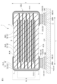
- the spacer 10 has recesses 11 formed on the surface of the second spacer main surface AS2, which is the mounting surface. A plurality of recesses 11 are formed.
- Fig. 4 is a view of the spacer 10 with the second spacer main surface AS2 facing up. According to this embodiment, by forming the recesses 11 on the surface on the second spacer main surface AS2 side, when the chip-type electronic component 1 is mounted on the mounting board 210, the solder 240 enters the recesses 11, and the fixing strength between the solder 240 and the spacer 10 can be improved by the anchor effect.
- the total opening area of the recesses 11 is preferably 25% or more and 75% or less of the surface area of the second spacer main surface AS2. The reason is that if the total opening area of the recesses 11 is greater than 75% of the area of the second spacer main surface AS2, much of the solder 240 is trapped in the recesses 11, making it difficult for the solder 240 to reach the spacer end surface CS and spacer side surface BS of the spacer 10, weakening the bonding strength between the spacer 10 and the mounting substrate 210.
- the total opening area of the recesses 11 is less than 25% of the entire area of the second spacer main surface AS2, the bonding area between the solder 240 and the spacer 10 is reduced, and therefore the anchor effect with the solder 240 cannot be obtained sufficiently.
- the total opening area of the recesses 11 of the spacer 10 is the sum of the areas of the openings of the recesses 11 when viewed from the second spacer main surface AS2 side.
- the second spacer main surface AS2 of the spacer 10 is not flat but has projections and recesses.
- the distance in the stacking direction T between the most protruding position on the second spacer main surface AS2 of the spacer 10, i.e., the top of the convex portion, and the first spacer main surface AS1 is defined as the thickness of the spacer 10. If the second spacer main surface AS2 is abutted against a flat surface, the flat surface abuts against the top of the convex portion of the second spacer main surface AS2.
- the portion within 1% of the thickness of the spacer 10 from the position of this flat surface, i.e., the top of the convex portion, toward the first spacer main surface AS1 is considered to be included in the flat surface of the second spacer main surface AS2, and the portion recessed by more than 1% of the thickness of the spacer 10 is defined as the recess 11.
- the opening area of one recess 11 is preferably 0.1% to 70% of the surface area of the second spacer main surface AS2. The reason is that if the opening area of one recess 11 is larger than 70% of the area of the second spacer main surface AS2, too much solder 240 is trapped in the recess 11, making it difficult for the solder 240 to reach the spacer end surface CS and spacer side surface BS of the spacer 10, which may reduce the bonding strength between the spacer 10 and the mounting substrate 210.
- the opening area of one recess 11 is smaller than 0.1% of the area of the second spacer main surface AS2, the solder 240 will not sufficiently enter the recess 11 of the spacer 10, and therefore will not be able to fully benefit from the anchor effect. Furthermore, the opening area of one recess 11 is more preferably 0.5% or more and 65% or less of the area of the second spacer main surface AS2, even more preferably 1% or more and 60% or less, and particularly preferably 5% or more and 50% or less.
- the number of recesses 11 is appropriately selected so as to satisfy the above conditions of the total opening area of the recesses 11 and the opening area of one recess 11 .
- Internal shape of recess 11 There is no particular limitation on the shape of the inside of the recess 11. For example, it may be a tapered shape that becomes narrower from the second spacer main surface AS2 toward the first spacer main surface AS1, or it may be an octopus pot shape in which the inside is larger than the opening.
- the depth of the recess 11 is preferably 1% to 50% of the thickness of the spacer 10 in the stacking direction T.
- the stacking direction T is the direction in which the dielectric layers 4 and the internal electrode layers 5 are stacked in the multilayer ceramic capacitor 1A described above, and in the case of the spacer 10, is the direction connecting the first spacer main surface AS1 and the second spacer main surface AS2.
- the "depth” refers to the length in the stacking direction T from the opening to the bottom of the recess 11.
- the depth of the recess 11 is preferably 1% or more of the thickness of the spacer 10 in the stacking direction T is that if the depth of the recess 11 is less than 1%, the surface will be smooth and it will be difficult to obtain the anchor effect described below.
- the depth of the recess 11 is 50% or less of the thickness of the spacer 10 in the stacking direction T is that if the depth of the recess 11 is greater than 50%, the length of the portion of the spacer 10 where the recess 11 is provided in the stacking direction T will be shortened, which may result in a decrease in the mechanical strength of the spacer 10.
- the recesses 11 are a mixture of recesses 11 of 1% or more and less than 5% and recesses 11 of 5% or more. Furthermore, the average depth of the recesses 11 of 5% or more is more preferably 5% or more and 35% or less, and even more preferably 10% or more and 20% or less, of the thickness of the spacer 10 in the stacking direction T. It is preferable that the recesses 11 are a mixture of recesses 11 of 1% or more and less than 5% and recesses 11 of 5% or more. The recesses 11 may be only recesses 11 of 1% or more and less than 5% or only recesses 11 of 5% or more.
- recesses 11 are formed also on the surfaces of two spacer end faces CS of the spacer 10 that face each other in the length direction L. It is also preferable that recesses 11 are formed also on the surfaces of two spacer side faces BS of the spacer 10 that face each other in the width direction W. In this way, when recesses 11 are arranged on the surface of the spacer end face CS and the surface of the spacer side face BS, the solder 240 wets onto the surface of the spacer end face CS and the spacer side face BS, thereby improving the adhesion between the solder 240 and the external electrode 3.
- the recesses 11 of the spacer 10 are provided on the second spacer main surface AS2, they do not have to be provided on other surfaces. Also, if they are provided on other surfaces, they may be located on some of the surfaces, not all of the surfaces.
- the “some surfaces” may be any surfaces.
- the recess 11 is provided on the second spacer main surface AS2, it may be arranged on both or one of the spacer side surfaces BS, or on both or one of the spacer end surfaces CS.
- the recess 11 is disposed on one side, it is more preferable that the recess 11 is formed on the end face CS1 of the first spacer 10A and the end face CS2 of the second spacer 10B.
- the solder 240 that wets and rises on the first spacer end face CS1 and the second spacer end face CS2 is absorbed by the recess 11 on the end face CS1 of the first spacer 10A and the recess 11 on the end face CS2 of the second spacer 10B, so that excessive fillet formation can be suppressed.
- the recess 11 of the spacer 10 may be disposed on different faces in the first spacer 10A and the second spacer 10B, so long as it is provided on the second spacer main surface AS2.
- a land 230 is arranged on a mounting substrate 210 on which the chip-type electronic component 1 is mounted.
- the land 230 has a first land 230A and a second land 230B.
- the first spacer 10A is connected to the first land 230A
- the second spacer 10B is connected to the second land 230B by solder 240, respectively.
- a recess 11 is formed on the surface on the second spacer main surface AS2 side, and solder 240 fills this recess 11. Therefore, the chip-type electronic component 1 and the mounting substrate 210 are bonded with high adhesion strength due to the anchor effect.
- the manufacturing process of the chip-type electronic component 1 includes a laminate manufacturing step S1, an external electrode forming step S2, a spacer arranging step S3, and a recess forming step S4.
- a material sheet is prepared in which a pattern of the internal electrode layer 5 is printed with a conductive paste on a ceramic green sheet for lamination, which is formed by forming a ceramic slurry into a sheet shape. Then, a plurality of material sheets are stacked so that the internal electrode patterns are shifted by half a pitch between adjacent material sheets in the longitudinal direction. Furthermore, outer layer ceramic green sheets that will become the outer layer parts are stacked on both sides of the plurality of stacked material sheets, and are thermocompression-bonded to form a mother block member. A plurality of laminates 2 are manufactured by dividing the mother block member along a cutting line corresponding to the dimensions of the laminate.
- a base electrode layer 30 is formed by, for example, applying a conductive paste containing a conductive metal and glass to both ends of the laminate 2 and baking it. As shown in Fig. 2, the base electrode layer 30 is formed so as to cover not only the capacitor end faces C on both sides of the laminate 2 but also extend to the capacitor main surface A side and cover a part of the capacitor main surface A on the capacitor end face C side.
- a Ni plating layer 31a is first formed on the outer periphery of the base electrode layer 30 so as to cover the base electrode layer 30.
- a Sn plating layer 31b is formed on the outer periphery of the Ni plating layer 31a so as to cover the Ni plating layer 31a.
- a multilayer ceramic capacitor 1A in which the external electrodes 3 are formed on the laminate 2 is manufactured.
- Spacer placement step S3 In the spacer arranging step S3, an intermetallic compound paste, which is the material of the spacer 10, is arranged on the outer periphery of the external electrode 3 on the second capacitor main surface A2 side of the multilayer ceramic capacitor 1A.
- the intermetallic compound paste is a so-called high temperature solder containing, as a main component, an intermetallic compound containing at least one of Cu and Ni as a high melting point metal and Sn as a low melting point metal.
- Such an intermetallic compound paste is once melted at 200° C. or higher and then placed in a liquid state on the surface of the Sn plating layer 31b.
- High temperature solder has a melting point that does not melt even at ordinary soldering temperatures, and it is possible to arrange the solder while maintaining the desired shape.
- the intermetallic compound paste is bonded to, for example, an alumina plate, which has a desired unevenness and is not to be bonded to the high-temperature solder, from the second main surface side.
- the alumina plate is removed. This allows the recess 11 to be formed on the second spacer main surface AS2 of the spacer 10.
- the recesses 11 on the spacer end faces CS and the spacer side faces BS can be formed by, for example, arranging an alumina plate so as to wrap around the end faces and the side faces.
- a method of abutting an alumina plate is preferable.
- a method of forming the recess 11 by sandblasting or the like is preferable.
- either method may be used to form the recess 11.
- the method for forming the recesses 11 is not limited to this, and other methods may be used.
- the recesses may be formed by roughening the hardened surface with, for example, a file, or by a chemical method such as etching. Through the above steps, the chip-type electronic component 1 is manufactured.
- the recess 11 is formed on the surface on the second spacer main surface AS2 side, so that when the chip-type electronic component 1 is mounted on the mounting substrate 210, the solder 240 enters the recess 11, and the anchor effect improves the adhesive strength between the solder 240 and the spacer 10.
- the solder 240 may not only be disposed between the spacer 10 and the land 230 as shown in FIG. 2, but may also cover the spacer 10 and the side of the external electrode 3 as shown in FIG. 6.
- the spacer 10 of the embodiment has recesses 11 formed on the surfaces of the spacer end faces CS and the spacer side faces BS. Therefore, when the solder 240 covers the spacer 10 and the side of the external electrode 3 as shown in FIG. 6, the solder 240 penetrates into the surface recesses 11 on the surfaces of the spacer end faces CS and the spacer side faces BS, and the stronger anchor effect can further improve the adhesive strength between the solder 240 and the spacer 10.
- a chip-type electronic component comprising: a laminate including a plurality of internal electrode layers and a plurality of internal dielectric layers arranged alternately with each other; a multilayer ceramic capacitor including external electrodes provided on each of the capacitor end faces, when two faces of the laminate opposing each other in a stacking direction are defined as capacitor main faces, two faces opposing each other in a width direction intersecting the stacking direction are defined as capacitor side faces, and two faces opposing each other in a length direction intersecting the stacking direction and the width direction are defined as capacitor end faces; and a spacer arranged on both sides in the length direction of the capacitor main face on a mounting substrate side of the multilayer ceramic capacitor, wherein a recess is formed on a surface of the spacer main face on the mounting substrate side when the two faces of the spacer opposing each other in the stacking direction are defined as spacer main faces.
- ⁇ 2> The chip-type electronic component described in ⁇ 1>, in which the spacer is mainly composed of an intermetallic compound containing a high melting point metal and a low melting point metal.
- ⁇ 3> The chip-type electronic component described in ⁇ 2>, in which the high melting point metal includes at least one of Cu and Ni, and the low melting point metal includes Sn.
- ⁇ 5> A chip-type electronic component according to any one of ⁇ 1> to ⁇ 4>, in which the total opening area of the recesses of the spacer is 25% to 75% of the surface area of the main surface of the spacer on the mounting substrate side.
- ⁇ 6> A chip-type electronic component according to any one of ⁇ 1> to ⁇ 5>, in which the opening area of one of the recesses of the spacer is 0.1% to 70% of the surface area of the main surface of the spacer on the mounting substrate side.
- ⁇ 7> A chip-type electronic component according to any one of ⁇ 1> to ⁇ 6>, in which the depth of the recess in the stacking direction is 1% to 50% of the thickness of the spacer in the stacking direction.
- ⁇ 8> A chip-type electronic component according to any one of ⁇ 1> to ⁇ 7>, in which the spacer has recesses formed on the surfaces of two spacer end faces CS that face each other in the longitudinal direction.
- a chip-type electronic component according to any one of ⁇ 1> to ⁇ 8>, in which the spacer has recesses formed on the surfaces of two spacer side surfaces that face each other in the width direction.
- the chip-type electronic component according to any one of ⁇ 1> to ⁇ 9>, in which one of the two capacitor end faces in the laminate is a first capacitor end face and the other is a second capacitor end face, the face of the two capacitor main faces facing the spacer is a second capacitor main face, and in each of the spacers, when the one of the two spacer end faces facing each other in the length direction is a first spacer end face and the other is a second spacer end face, the spacer has a first spacer that contacts a portion of the first external electrode arranged on the side of the first capacitor end face that extends toward the second capacitor main face, and a second spacer that contacts a portion of the second external electrode arranged on the side of the second capacitor end face that extends toward the second capacitor main face, and a recess is formed in the first spacer end face, which is the face of the first spacer that faces the first capacitor end face, and a recess is formed in the second spacer end face, which is the face of the second spacer that faces
Abstract
Provided is a chip-type electronic component that is less likely to cause separation of a spacer and a mounting substrate. A chip-type electronic component 1 of the present invention comprises a multilayered ceramic capacitor 1A and spacers 10. The multilayered ceramic capacitor 1A comprises: a stack 2 that includes internal electrode layers 5 and dielectric layers 4 that are alternately disposed; and external electrodes 3. When the two surfaces of the stack 2 opposing each other in the multilayered direction are capacitor main surfaces A, the two surfaces thereof opposing each other in the width direction are capacitor side surfaces B, and the two surfaces thereof opposing each other in the length direction are capacitor end surfaces C, the external electrodes 3 are respectively provided on the capacitor end surfaces C. The spacers 10 are disposed on both sides in the length direction of the capacitor main surface A on the mounting substrate side of the multilayered ceramic capacitor 1A. When the two surfaces opposing each other in the multilayered direction of each of the spacers 10 are spacer main surfaces AS, a recess 11 is formed in the surface of the spacer main surface AS on the mounting substrate side.
Description
本発明は、チップ型電子部品に関する。
The present invention relates to chip-type electronic components.
積層セラミックコンデンサは、誘電体層と内部電極とが交互に積み重ねられた内層部を有する積層体と、積層体の長手方向の両端面に設けられた外部電極とを有する。ここで、積層セラミックコンデンサに電圧を印加すると、誘電体層が分極し、積層セラミックコンデンサが分極方向に振動する場合がある。そうすると、この振動が実装基板に伝わり、実装基板にクラックが発生してしまう可能性がある。このため、従来、積層セラミックコンデンサの実装面側にスペーサを配置してチップ型電子部品とし、スペーサによって振動を緩衝し、実装基板に伝わる振動を抑える技術がある(特許文献1参照)。
A multilayer ceramic capacitor has a laminate having an inner layer in which dielectric layers and internal electrodes are alternately stacked, and external electrodes provided on both longitudinal end faces of the laminate. When a voltage is applied to the multilayer ceramic capacitor, the dielectric layers are polarized, and the multilayer ceramic capacitor may vibrate in the polarization direction. This vibration may then be transmitted to the mounting board, potentially causing cracks in the mounting board. For this reason, there is a conventional technology in which a spacer is placed on the mounting surface side of the multilayer ceramic capacitor to make it a chip-type electronic component, and the spacer cushions the vibration and suppresses the vibration transmitted to the mounting board (see Patent Document 1).
しかし、例えば誘電体層の成分として高誘電率なものを使用すると、振動が大きくなる。このため、実装基板とスペーサとの間の接合力が弱いと、スペーサが実装基板から剥離する可能性がある。
However, for example, if a component with a high dielectric constant is used as the dielectric layer component, vibrations will increase. Therefore, if the bonding strength between the mounting board and the spacer is weak, the spacer may peel off from the mounting board.
本発明の課題は、スペーサと実装基板とが剥離しにくいチップ型電子部品を提供することである。
The objective of the present invention is to provide a chip-type electronic component in which the spacer is less likely to peel off from the mounting substrate.
上記課題を解決するために、本発明は、互いに交互に配置された複数の内部電極層と複数の内部誘電体層とを含む積層体、及び、前記積層体の、積層方向において互いに対向する2つの面をコンデンサ主面、前記積層方向と交差する幅方向において互いに対向する2つの面をコンデンサ側面、前記積層方向と前記幅方向とに交差する長さ方向において互いに対向する2つの面をコンデンサ端面、としたときに、前記コンデンサ端面のそれぞれ設けられた外部電極、を備える積層セラミックコンデンサと、前記積層セラミックコンデンサの実装基板側の前記コンデンサ主面における、前記長さ方向の両側に配置されたスペーサと、を備えるチップ型電子部品であって、前記スペーサにおける、前記積層方向において互いに対向する2つの面をスペーサ主面としたときに、実装基板側の前記スペーサ主面の表面に、凹部が形成されている、チップ型電子部品を提供する。
In order to solve the above problems, the present invention provides a chip-type electronic component comprising: a laminate including a plurality of internal electrode layers and a plurality of internal dielectric layers arranged alternately with each other; a multilayer ceramic capacitor including external electrodes provided on each of the capacitor end faces when two surfaces of the laminate opposing each other in the lamination direction are defined as capacitor main faces, two surfaces opposing each other in a width direction intersecting with the lamination direction are defined as capacitor side faces, and two surfaces opposing each other in a length direction intersecting with the lamination direction and the width direction are defined as capacitor end faces; and a spacer disposed on both sides in the length direction of the capacitor main face on the mounting substrate side of the multilayer ceramic capacitor, wherein a recess is formed on the surface of the spacer main face on the mounting substrate side when the two surfaces of the spacer opposing each other in the lamination direction are defined as spacer main faces.
本発明によれば、スペーサと実装基板とが剥離しにくいチップ型電子部品を提供することができる。
The present invention provides a chip-type electronic component in which the spacer is less likely to peel off from the mounting substrate.
以下、本発明の実施形態について説明する。図1は、実施形態に係るチップ型電子部品1の概略斜視図である。図2は、チップ型電子部品1の図1におけるII-II線に沿った部分断面図である。図3は、チップ型電子部品1の図1におけるIII-III線に沿った断面図である。図1、図2及び図3は、実装基板210上に接合された状態を示す。
The following describes an embodiment of the present invention. Fig. 1 is a schematic perspective view of a chip-type electronic component 1 according to an embodiment. Fig. 2 is a partial cross-sectional view of the chip-type electronic component 1 taken along line II-II in Fig. 1. Fig. 3 is a cross-sectional view of the chip-type electronic component 1 taken along line III-III in Fig. 1. Figs. 1, 2, and 3 show the chip-type electronic component 1 bonded onto a mounting substrate 210.
チップ型電子部品1は、略直方体形状の積層体2と、積層体2の両端に設けられた一対の外部電極3とを備える積層セラミックコンデンサ1A、及び、積層セラミックコンデンサ1Aに取り付けられたスペーサ10を備える。また、積層体2は、誘電体層4と内部電極層5とを複数組含む内層部6を含む。
The chip-type electronic component 1 comprises a laminated ceramic capacitor 1A having a laminate 2 of a substantially rectangular parallelepiped shape and a pair of external electrodes 3 provided on both ends of the laminate 2, and a spacer 10 attached to the laminated ceramic capacitor 1A. The laminate 2 also includes an inner layer 6 including multiple pairs of dielectric layers 4 and internal electrode layers 5.
以下の説明において、チップ型電子部品1の向きを表わす用語として、一対の外部電極3が設けられている方向を長さ方向Lとする。誘電体層4と内部電極層5とが積層されている方向を積層方向Tとする。長さ方向L及び積層方向Tのいずれにも交差する方向を幅方向Wとする。なお、実施形態においては、幅方向Wは長さ方向L及び積層方向Tのいずれにも直交している。
In the following description, the direction in which the pair of external electrodes 3 are provided is referred to as the length direction L, and the direction in which the dielectric layers 4 and the internal electrode layers 5 are stacked is referred to as the stacking direction T. The direction that intersects both the length direction L and the stacking direction T is referred to as the width direction W. Note that in this embodiment, the width direction W is perpendicular to both the length direction L and the stacking direction T.
また、積層体2の6つの外表面のうち、積層方向Tに相対する一対の外表面を第1コンデンサ主面A1と第2コンデンサ主面A2とし、幅方向Wに相対する一対の外表面を第1コンデンサ側面B1と第2コンデンサ側面B2とし、長さ方向Lに相対する一対の外表面を第1コンデンサ端面C1と第2コンデンサ端面C2とする。
Furthermore, of the six outer surfaces of the laminate 2, a pair of outer surfaces facing each other in the stacking direction T are the first capacitor main surface A1 and the second capacitor main surface A2, a pair of outer surfaces facing each other in the width direction W are the first capacitor side surface B1 and the second capacitor side surface B2, and a pair of outer surfaces facing each other in the length direction L are the first capacitor end surface C1 and the second capacitor end surface C2.
なお、第1コンデンサ主面A1と第2コンデンサ主面A2とを特に区別して説明する必要のない場合、まとめてコンデンサ主面Aとし、第1コンデンサ側面B1と第2コンデンサ側面B2とを特に区別して説明する必要のない場合、まとめてコンデンサ側面Bとし、第1コンデンサ端面C1と第2コンデンサ端面C2とを特に区別して説明する必要のない場合、まとめてコンデンサ端面Cとして説明する。
Note that when there is no need to distinguish between the first capacitor main surface A1 and the second capacitor main surface A2, they will be collectively referred to as the capacitor main surface A, when there is no need to distinguish between the first capacitor side surface B1 and the second capacitor side surface B2, they will be collectively referred to as the capacitor side surface B, and when there is no need to distinguish between the first capacitor end surface C1 and the second capacitor end surface C2, they will be collectively referred to as the capacitor end surface C.
(積層体2)
積層体2は、内層部6と、内層部6のコンデンサ主面A側に配置される外層部7と、サイドギャップ部8と、を備える。積層体2は、稜線部Rに丸みがつけられていることが好ましい。稜線部Rは、積層体2の2面、すなわちコンデンサ主面Aとコンデンサ側面B、コンデンサ主面Aとコンデンサ端面C、又は、コンデンサ側面Bとコンデンサ端面Cが交わる部分であり、コンデンサ主面Aとコンデンサ側面Bとコンデンサ端面Cとが交わる角部も含む。 (Laminate 2)
Thelaminate 2 includes an inner layer portion 6, an outer layer portion 7 disposed on the capacitor main surface A side of the inner layer portion 6, and a side gap portion 8. The laminate 2 preferably has rounded ridge portions R. The ridge portions R are portions where two surfaces of the laminate 2, i.e., the capacitor main surface A and the capacitor side surface B, the capacitor main surface A and the capacitor end surface C, or the capacitor side surface B and the capacitor end surface C, intersect, and also include corners where the capacitor main surface A, the capacitor side surface B, and the capacitor end surface C intersect.
積層体2は、内層部6と、内層部6のコンデンサ主面A側に配置される外層部7と、サイドギャップ部8と、を備える。積層体2は、稜線部Rに丸みがつけられていることが好ましい。稜線部Rは、積層体2の2面、すなわちコンデンサ主面Aとコンデンサ側面B、コンデンサ主面Aとコンデンサ端面C、又は、コンデンサ側面Bとコンデンサ端面Cが交わる部分であり、コンデンサ主面Aとコンデンサ側面Bとコンデンサ端面Cとが交わる角部も含む。 (Laminate 2)
The
(内層部6)
内層部6は、積層方向Tに沿って交互に積層された誘電体層4と内部電極層5とを複数組含む。 (Inner layer 6)
Theinner layer portion 6 includes a plurality of pairs of dielectric layers 4 and internal electrode layers 5 alternately stacked along the stacking direction T.
内層部6は、積層方向Tに沿って交互に積層された誘電体層4と内部電極層5とを複数組含む。 (Inner layer 6)
The
(誘電体層4)
誘電体層4は、セラミック材料で製造されている。セラミック材料としては、例えば、BaTiO3を主成分とする誘電体セラミックが用いられる。また、セラミック材料として、これらの主成分にMn化合物、Fe化合物、Cr化合物、Co化合物、ニッケル化合物等の副成分のうちの少なくとも1つを添加したものを用いてもよい。 (Dielectric layer 4)
Thedielectric layer 4 is made of a ceramic material. For example, a dielectric ceramic containing BaTiO3 as a main component is used as the ceramic material. Alternatively, the ceramic material may be one containing at least one of a Mn compound, an Fe compound, a Cr compound, a Co compound, a Nickel compound, or the like, added to the main component.
誘電体層4は、セラミック材料で製造されている。セラミック材料としては、例えば、BaTiO3を主成分とする誘電体セラミックが用いられる。また、セラミック材料として、これらの主成分にMn化合物、Fe化合物、Cr化合物、Co化合物、ニッケル化合物等の副成分のうちの少なくとも1つを添加したものを用いてもよい。 (Dielectric layer 4)
The
(内部電極層5)
内部電極層5は、例えばニッケル、Cu、Ag、Pd、Ag-Pd合金、Au等に代表される金属材料により形成されていることが好ましい。 (Internal electrode layer 5)
Theinternal electrode layers 5 are preferably made of a metal material typified by, for example, nickel, Cu, Ag, Pd, an Ag-Pd alloy, Au, and the like.
内部電極層5は、例えばニッケル、Cu、Ag、Pd、Ag-Pd合金、Au等に代表される金属材料により形成されていることが好ましい。 (Internal electrode layer 5)
The
内部電極層5は、複数の第1内部電極層5Aと、複数の第2内部電極層5Bとを備える。第1内部電極層5Aと第2内部電極層5Bとは、交互に配置されている。なお、第1内部電極層5Aと第2内部電極層5Bとを特に区別して説明する必要のない場合、まとめて内部電極層5として説明する。
The internal electrode layer 5 comprises a plurality of first internal electrode layers 5A and a plurality of second internal electrode layers 5B. The first internal electrode layers 5A and the second internal electrode layers 5B are arranged alternately. Note that, when there is no need to distinguish between the first internal electrode layers 5A and the second internal electrode layers 5B, they will be collectively referred to as the internal electrode layer 5.
内部電極層5は、第1内部電極層5Aと第2内部電極層5Bとの間で互いに対向する対向部52と、第1内部電極層5Aと第2内部電極層5Bとの間で互いに対向せず、対向部52から一方のコンデンサ端面C側に引き出された引出部51とを備える。引出部51の端部は、コンデンサ端面Cに露出し、外部電極3に電気的に接続されている。引出部51が延びる方向は、第1内部電極層5Aと第2内部電極層5Bとで異なり、第1コンデンサ端面C1側と第2コンデンサ端面C2側とに交互に引き出される。そして、積層方向Tに隣り合う第1内部電極層5Aと第2内部電極層5Bとの対向部52間に電荷が蓄積され、コンデンサとして機能する。
The internal electrode layer 5 has opposing portions 52 that face each other between the first internal electrode layer 5A and the second internal electrode layer 5B, and lead-out portions 51 that do not face each other between the first internal electrode layer 5A and the second internal electrode layer 5B and are drawn out from the opposing portions 52 to one of the capacitor end faces C. The ends of the lead-out portions 51 are exposed to the capacitor end face C and are electrically connected to the external electrode 3. The extending directions of the lead-out portions 51 differ between the first internal electrode layer 5A and the second internal electrode layer 5B, and the lead-out portions 51 are drawn out alternately to the first capacitor end face C1 side and the second capacitor end face C2 side. An electric charge is accumulated between the opposing portions 52 of the first internal electrode layer 5A and the second internal electrode layer 5B that are adjacent to each other in the stacking direction T, and function as a capacitor.
(外層部7)
外層部7は、内層部6の両コンデンサ主面A側にそれぞれ配置され、内層部6の誘電体層4と同じ材料で製造されている。 (Outer layer 7)
Theouter layer portions 7 are disposed on both capacitor main surface A sides of the inner layer portion 6 , and are made of the same material as the dielectric layers 4 of the inner layer portions 6 .
外層部7は、内層部6の両コンデンサ主面A側にそれぞれ配置され、内層部6の誘電体層4と同じ材料で製造されている。 (Outer layer 7)
The
(サイドギャップ部8)
サイドギャップ部8は、積層体2における内層部6の両コンデンサ側面B側に設けられている。サイドギャップ部8は、誘電体層4と同じ材料で一体的に製造されている。 (Side gap portion 8)
Theside gaps 8 are provided on both capacitor side surfaces B of the inner layer portion 6 in the laminate 2. The side gaps 8 are integrally manufactured from the same material as the dielectric layers 4.
サイドギャップ部8は、積層体2における内層部6の両コンデンサ側面B側に設けられている。サイドギャップ部8は、誘電体層4と同じ材料で一体的に製造されている。 (Side gap portion 8)
The
(外部電極3)
外部電極3は、積層体2の両コンデンサ端面Cに設けられている。つまり、第1コンデンサ端面C1には第1外部電極3Aが形成され、第2コンデンサ端面C2には第2外部電極3Bが形成されている。外部電極3は、コンデンサ端面Cだけでなく、コンデンサ主面A及びコンデンサ側面Bのコンデンサ端面C側の一部も覆っている。外部電極3は、下地電極層30と、下地電極層30の外周に形成されためっき層31とを含む。 (External electrode 3)
Theexternal electrodes 3 are provided on both capacitor end faces C of the laminate 2. That is, a first external electrode 3A is formed on the first capacitor end face C1, and a second external electrode 3B is formed on the second capacitor end face C2. The external electrodes 3 cover not only the capacitor end face C, but also a portion of the capacitor main face A and the capacitor side face B on the capacitor end face C side. The external electrodes 3 include a base electrode layer 30 and a plating layer 31 formed on the outer periphery of the base electrode layer 30.
外部電極3は、積層体2の両コンデンサ端面Cに設けられている。つまり、第1コンデンサ端面C1には第1外部電極3Aが形成され、第2コンデンサ端面C2には第2外部電極3Bが形成されている。外部電極3は、コンデンサ端面Cだけでなく、コンデンサ主面A及びコンデンサ側面Bのコンデンサ端面C側の一部も覆っている。外部電極3は、下地電極層30と、下地電極層30の外周に形成されためっき層31とを含む。 (External electrode 3)
The
(下地電極層30)
下地電極層30は、コンデンサ端面Cに露出した内部電極層5の引出部51の端部に電気的に接続されている。実施形態で下地電極層30は、例えば、銅、ニッケル、銀、パラジウム、銀-パラジウム合金、金等の導電性金属を含む導電性ペーストを焼成した、いわゆる焼き付け電極であり、焼き付け電極はガラス成分と金属とを含む。ガラス成分は、B、Si、Ba、Mg、Al、Li等から選ばれる少なくとも1つを含む。焼き付け電極は、ガラスおよび金属を含む導電性ペーストを積層体2に塗布して焼き付けたものであり、内部電極層5および誘電体層4と同時焼成したものでもよく、内部電極層5を焼成した後に焼き付けてもよい。なお、内部電極層5および誘電体層4と同時に焼成する場合には、ガラス成分の代わりに誘電体材料を添加して焼き付け電極を形成することが好ましい。 (Underlying electrode layer 30)
Thebase electrode layer 30 is electrically connected to the end of the lead portion 51 of the internal electrode layer 5 exposed on the capacitor end surface C. In the embodiment, the base electrode layer 30 is a so-called baked electrode obtained by baking a conductive paste containing a conductive metal such as copper, nickel, silver, palladium, a silver-palladium alloy, or gold, and the baked electrode contains a glass component and a metal. The glass component contains at least one selected from B, Si, Ba, Mg, Al, Li, and the like. The baked electrode is obtained by applying a conductive paste containing glass and a metal to the laminate 2 and baking it, and may be baked simultaneously with the internal electrode layer 5 and the dielectric layer 4, or may be baked after the internal electrode layer 5 is baked. When the internal electrode layer 5 and the dielectric layer 4 are baked simultaneously, it is preferable to add a dielectric material instead of the glass component to form the baked electrode.
下地電極層30は、コンデンサ端面Cに露出した内部電極層5の引出部51の端部に電気的に接続されている。実施形態で下地電極層30は、例えば、銅、ニッケル、銀、パラジウム、銀-パラジウム合金、金等の導電性金属を含む導電性ペーストを焼成した、いわゆる焼き付け電極であり、焼き付け電極はガラス成分と金属とを含む。ガラス成分は、B、Si、Ba、Mg、Al、Li等から選ばれる少なくとも1つを含む。焼き付け電極は、ガラスおよび金属を含む導電性ペーストを積層体2に塗布して焼き付けたものであり、内部電極層5および誘電体層4と同時焼成したものでもよく、内部電極層5を焼成した後に焼き付けてもよい。なお、内部電極層5および誘電体層4と同時に焼成する場合には、ガラス成分の代わりに誘電体材料を添加して焼き付け電極を形成することが好ましい。 (Underlying electrode layer 30)
The
(めっき層31)
めっき層31は、下地電極層30の外周に、下地電極層30を覆うように配置されているNiめっき層31aと、Niめっき層31aの外周に、Niめっき層31aを覆うように配置されているSnめっき層31bとを含む。Niめっき層31aは、下地電極層30がセラミック電子部品を実装する際の半田によって侵食されることを防止することができ、Snめっき層31bは、積層セラミックコンデンサ1Aを実装する際の半田の濡れ性を向上させ、容易に実装することができる。Niめっき層31aは、ニッケル又はニッケルを含む合金のめっきからなる。Snめっき層31bはSn又はSnを含む合金のめっきからなる。めっき層31は上記金属以外に、例えば、Cu、Ni、Sn、Ag、Pd、Ag-Pd合金、Au等から選ばれる少なくとも1つを含んでいてもよい。 (Plating layer 31)
Theplating layer 31 includes a Ni plating layer 31a disposed around the outer periphery of the base electrode layer 30 so as to cover the base electrode layer 30, and a Sn plating layer 31b disposed around the outer periphery of the Ni plating layer 31a so as to cover the Ni plating layer 31a. The Ni plating layer 31a can prevent the base electrode layer 30 from being eroded by solder when mounting a ceramic electronic component, and the Sn plating layer 31b improves the wettability of the solder when mounting the multilayer ceramic capacitor 1A, allowing easy mounting. The Ni plating layer 31a is made of nickel or a plating of an alloy containing nickel. The Sn plating layer 31b is made of Sn or a plating of an alloy containing Sn. In addition to the above metals, the plating layer 31 may contain at least one selected from, for example, Cu, Ni, Sn, Ag, Pd, an Ag-Pd alloy, Au, and the like.
めっき層31は、下地電極層30の外周に、下地電極層30を覆うように配置されているNiめっき層31aと、Niめっき層31aの外周に、Niめっき層31aを覆うように配置されているSnめっき層31bとを含む。Niめっき層31aは、下地電極層30がセラミック電子部品を実装する際の半田によって侵食されることを防止することができ、Snめっき層31bは、積層セラミックコンデンサ1Aを実装する際の半田の濡れ性を向上させ、容易に実装することができる。Niめっき層31aは、ニッケル又はニッケルを含む合金のめっきからなる。Snめっき層31bはSn又はSnを含む合金のめっきからなる。めっき層31は上記金属以外に、例えば、Cu、Ni、Sn、Ag、Pd、Ag-Pd合金、Au等から選ばれる少なくとも1つを含んでいてもよい。 (Plating layer 31)
The
(スペーサ10)
スペーサ10は、一対の2つのスペーサである第1スペーサ10Aと第2スペーサ10Bとを備える。以下、第1スペーサ10Aと、第2スペーサ10Bとを区別して説明する必要のない場合、スペーサ10として説明する。積層セラミックコンデンサ1Aの第2コンデンサ主面A2側における、長さ方向Lの一方に第1スペーサ10Aが配置され、他方に第2スペーサ10Bが配置されている。第1スペーサ10Aと第2スペーサ10Bとは互いに略矩形の同形であって対向し、一定の距離、離間して配置されている。 (Spacer 10)
Thespacer 10 includes a pair of two spacers, a first spacer 10A and a second spacer 10B. Hereinafter, when there is no need to distinguish between the first spacer 10A and the second spacer 10B, they will be described as the spacer 10. The first spacer 10A is disposed on one side of the second capacitor main surface A2 of the multilayer ceramic capacitor 1A in the length direction L, and the second spacer 10B is disposed on the other side. The first spacer 10A and the second spacer 10B have the same shape of a substantially rectangular shape, face each other, and are disposed at a certain distance apart.
スペーサ10は、一対の2つのスペーサである第1スペーサ10Aと第2スペーサ10Bとを備える。以下、第1スペーサ10Aと、第2スペーサ10Bとを区別して説明する必要のない場合、スペーサ10として説明する。積層セラミックコンデンサ1Aの第2コンデンサ主面A2側における、長さ方向Lの一方に第1スペーサ10Aが配置され、他方に第2スペーサ10Bが配置されている。第1スペーサ10Aと第2スペーサ10Bとは互いに略矩形の同形であって対向し、一定の距離、離間して配置されている。 (Spacer 10)
The
スペーサ10は、略直方体でで、6つの外表面のうち、積層方向Tに相対する一対の外表面を第1スペーサ主面AS1と第2スペーサ主面AS2とし、幅方向Wに相対する一対の外表面を第1スペーサ側面BS1と第2スペーサ側面BS2とし、長さ方向Lに相対する一対の外表面を第1スペーサ端面CS1と第2スペーサ端面CS2とする。
The spacer 10 is a roughly rectangular parallelepiped, and of the six outer surfaces, a pair of outer surfaces that face each other in the stacking direction T are the first spacer main surface AS1 and the second spacer main surface AS2, a pair of outer surfaces that face each other in the width direction W are the first spacer side surface BS1 and the second spacer side surface BS2, and a pair of outer surfaces that face each other in the length direction L are the first spacer end surface CS1 and the second spacer end surface CS2.
第1スペーサ主面AS1は、積層体2側の面であり、第2スペーサ主面AS2は、実装基板210に実装される実装面である。
第1スペーサ10Aの第1スペーサ主面AS1は、第1コンデンサ端面C1に形成された第1の外部電極の第2コンデンサ主面A2側と接し、第2スペーサ10Bの第1スペーサ主面AS1は、第2コンデンサ端面C2に形成された第1の外部電極の第2コンデンサ主面A2側と接している。 The first spacer main surface AS 1 is the surface on thelaminate 2 side, and the second spacer main surface AS 2 is the mounting surface to be mounted on the mounting substrate 210 .
The first spacer main surface AS1 of thefirst spacer 10A contacts the second capacitor main surface A2 side of the first external electrode formed on the first capacitor end surface C1, and the first spacer main surface AS1 of the second spacer 10B contacts the second capacitor main surface A2 side of the first external electrode formed on the second capacitor end surface C2.
第1スペーサ10Aの第1スペーサ主面AS1は、第1コンデンサ端面C1に形成された第1の外部電極の第2コンデンサ主面A2側と接し、第2スペーサ10Bの第1スペーサ主面AS1は、第2コンデンサ端面C2に形成された第1の外部電極の第2コンデンサ主面A2側と接している。 The first spacer main surface AS 1 is the surface on the
The first spacer main surface AS1 of the
スペーサ10の積層方向Tと直交する断面形状は、長さ方向Lに延びる辺が短辺で、幅方向Wに延びる辺が長辺となる長方形である。第1スペーサ側面BS1及び第2スペーサ側面BS2は、スペーサ10の短辺に沿った面であり、第1スペーサ端面CS1及び第2スペーサ端面CS2は、スペーサ10の短辺に沿った面である。
第1スペーサ10Aの第1スペーサ端面CS1は、第1外部電極3Aの第1コンデンサ端面C1側に形成され、第2スペーサ10Bの第2スペーサ端面CS2は、第2外部電極3Bの第2コンデンサ端面C2側に形成されている。 The cross-sectional shape of thespacer 10 perpendicular to the stacking direction T is a rectangle whose short sides extend in the length direction L and whose long sides extend in the width direction W. The first spacer side surface BS1 and the second spacer side surface BS2 are surfaces along the short sides of the spacer 10, and the first spacer end surface CS1 and the second spacer end surface CS2 are surfaces along the short sides of the spacer 10.
The first spacer end face CS1 of thefirst spacer 10A is formed on the first capacitor end face C1 side of the first external electrode 3A, and the second spacer end face CS2 of the second spacer 10B is formed on the second capacitor end face C2 side of the second external electrode 3B.
第1スペーサ10Aの第1スペーサ端面CS1は、第1外部電極3Aの第1コンデンサ端面C1側に形成され、第2スペーサ10Bの第2スペーサ端面CS2は、第2外部電極3Bの第2コンデンサ端面C2側に形成されている。 The cross-sectional shape of the
The first spacer end face CS1 of the
なお、第1スペーサ主面AS1と第2スペーサ主面AS2とを特に区別して説明する必要のない場合、まとめてスペーサ主面ASとし、第1スペーサ側面BS1と第2スペーサ側面BS2とを特に区別して説明する必要のない場合、まとめてスペーサ側面BSとし、第1スペーサ端面CS1と第2スペーサ端面CS2とを特に区別して説明する必要のない場合、まとめてスペーサ端面CSとして説明する。
Note that when there is no need to distinguish between the first spacer main surface AS1 and the second spacer main surface AS2, they will be collectively referred to as the spacer main surface AS, when there is no need to distinguish between the first spacer side surface BS1 and the second spacer side surface BS2, they will be collectively referred to as the spacer side surface BS, and when there is no need to distinguish between the first spacer end surface CS1 and the second spacer end surface CS2, they will be collectively referred to as the spacer end surface CS.
スペーサ10は、直方体形状に限らず、第1スペーサ主面AS1が第2スペーサ主面AS2より面積が大きい他の六面体形状であってもよい。また、スペーサ側面BS及びスペーサ端面CSは、実装面である第2スペーサ主面AS2に対して垂直に配置されていなくてもよい。さらに、例えば第1スペーサ側面BS1、第2スペーサ側面BS2、第1スペーサ端面CS1及び第2スペーサ端面CS2等は、湾曲面であってもよい。
The spacer 10 is not limited to a rectangular parallelepiped shape, and may be another hexahedral shape in which the first spacer main surface AS1 has a larger area than the second spacer main surface AS2. Furthermore, the spacer side surface BS and the spacer end surface CS do not have to be arranged perpendicular to the second spacer main surface AS2, which is the mounting surface. Furthermore, for example, the first spacer side surface BS1, the second spacer side surface BS2, the first spacer end surface CS1, and the second spacer end surface CS2, etc. may be curved surfaces.
スペーサ10は、高融点金属と、低融点金属とを含む金属間化合物を主成分とする、いわゆる高温半田で製造されている。本明細書において、主成分とするとは、含有率が50%以上であることをいう。金属間化合物を主成分とすると、反応速度が速く、形状の変化が少ない。
The spacer 10 is made of so-called high-temperature solder, whose main component is an intermetallic compound containing a high melting point metal and a low melting point metal. In this specification, "main component" means that the content is 50% or more. When the main component is an intermetallic compound, the reaction speed is fast and there is little change in shape.
高融点金属は、Cu又はNiのうちの少なくとも一種を含み、低融点金属は、Snを含む。このようにCu又はNiのうちの少なくとも一種を含む高融点金属と、Snを含む低融点金属と、を含む金属間化合物を主成分とした場合、半田付けの温度でも溶融しない融点を持ち、半田付けの際にも所望の形態を保ったまま配置することが可能である。さらに、金属間化合物としては、特に、SnとCu-Ni合金との反応により生成された金属間化合物であることが好ましい。また、金属間化合物を構成する高融点金属として、Agをさらに含んでいてもよい。
The high melting point metal includes at least one of Cu and Ni, and the low melting point metal includes Sn. In this way, when the main component is an intermetallic compound including a high melting point metal including at least one of Cu and Ni, and a low melting point metal including Sn, it has a melting point that does not melt even at the soldering temperature, and it is possible to arrange it while maintaining the desired shape even during soldering. Furthermore, it is particularly preferable for the intermetallic compound to be an intermetallic compound generated by the reaction of Sn with a Cu-Ni alloy. Furthermore, the high melting point metal that constitutes the intermetallic compound may further include Ag.
(導電性樹脂)
また、スペーサ10は、導電性樹脂で製造されていてもよい。導電性樹脂は、金属と熱硬化性の樹脂とを含む。スペーサ10を導電性樹脂で製造した場合、樹脂を含むため、例えばめっき膜や導電性ペーストの焼成物からなる導電層よりも柔軟性に富んでいる。 (Conductive resin)
Thespacer 10 may be made of a conductive resin. The conductive resin contains a metal and a thermosetting resin. When the spacer 10 is made of a conductive resin, the spacer 10 is more flexible than a conductive layer made of, for example, a plating film or a sintered product of a conductive paste, because the spacer 10 contains resin.
また、スペーサ10は、導電性樹脂で製造されていてもよい。導電性樹脂は、金属と熱硬化性の樹脂とを含む。スペーサ10を導電性樹脂で製造した場合、樹脂を含むため、例えばめっき膜や導電性ペーストの焼成物からなる導電層よりも柔軟性に富んでいる。 (Conductive resin)
The
(導電性樹脂の金属)
導電性樹脂に含まれる金属としては、Ag、Cu、又はそれらの合金を使用することができる。また、金属粉の表面にAgコーティングされたものを使用することができる。金属粉の表面にAgコーティングされたものを使用する際には金属粉としてCuやNiを用いることが好ましい。またCuに酸化防止処理を施したものを使用することもできる。導電性樹脂に含まれる金属は、導電性樹脂全体の体積に対して、35vol%以上75vol%以下で含まれていることが好ましい。導電性樹脂に含まれる金属は、球形状、扁平状等のものを用いることができるが、球形状金属粉と扁平状金属粉とを混合して用いるのが好ましい。導電性樹脂に含まれる金属の平均粒径は、特に限定されない。導電性フィラーの平均粒径は、例えば、0.3μm以上10μm以下程度であってもよい。導電性樹脂に含まれる金属は、主に導電性樹脂の通電性を担う。具体的には、導電性フィラー同士が接触することにより、導電性樹脂内部に通電経路が形成される。 (Conductive resin metal)
The metal contained in the conductive resin can be Ag, Cu, or an alloy thereof. Also, a metal powder with Ag coating on the surface can be used. When using a metal powder with Ag coating on the surface, it is preferable to use Cu or Ni as the metal powder. Also, Cu with an oxidation prevention treatment can be used. The metal contained in the conductive resin is preferably contained in an amount of 35 vol% or more and 75 vol% or less with respect to the total volume of the conductive resin. The metal contained in the conductive resin can be spherical, flat, or the like, but it is preferable to use a mixture of spherical metal powder and flat metal powder. The average particle size of the metal contained in the conductive resin is not particularly limited. The average particle size of the conductive filler may be, for example, about 0.3 μm or more and 10 μm or less. The metal contained in the conductive resin mainly carries out the electrical conductivity of the conductive resin. Specifically, the conductive fillers come into contact with each other to form an electrical path inside the conductive resin.
(導電性樹脂の樹脂)
導電性樹脂に含まれる樹脂としては、例えば、エポキシ樹脂、フェノール樹脂、ウレタン樹脂、シリコーン樹脂、ポリイミド樹脂等の公知の種々の熱硬化性樹脂を使用することができる。その中でも、耐熱性、耐湿性、密着性等に優れたエポキシ樹脂は最も適切な樹脂の1つである。導電性樹脂に含まれる樹脂は、導電性樹脂全体の体積に対して、25vol%以上65vol%以下で含まれていることが好ましい。また、導電性樹脂には、熱硬化性樹脂とともに、硬化剤を含むことが好ましい。硬化剤としては、ベース樹脂としてエポキシ樹脂を用いる場合、エポキシ樹脂の硬化剤としては、フェノール系、アミン系、酸無水物系、イミダゾール系等公知の種々の化合物を使用することができる。 (Conductive resin)
As the resin contained in the conductive resin, various known thermosetting resins such as epoxy resin, phenol resin, urethane resin, silicone resin, polyimide resin, etc. can be used. Among them, epoxy resin, which has excellent heat resistance, moisture resistance, adhesion, etc., is one of the most suitable resins. The resin contained in the conductive resin is preferably contained in an amount of 25 vol% or more and 65 vol% or less with respect to the total volume of the conductive resin. In addition, the conductive resin preferably contains a curing agent together with the thermosetting resin. As the curing agent, when an epoxy resin is used as the base resin, various known compounds such as phenol-based, amine-based, acid anhydride-based, and imidazole-based compounds can be used as the curing agent for the epoxy resin.
(表面形状)
スペーサ10は、実装面である第2スペーサ主面AS2の表面に、凹部11が形成されている。凹部11は複数個形成されている。図4は、スペーサ10の第2スペーサ主面AS2を上にした図である。本実施形態によると、第2スペーサ主面AS2側の表面に凹部11が形成されていることで、チップ型電子部品1を実装基板210に実装する際、半田240が凹部11に入り込み、アンカー効果によって半田240とスペーサ10との固着力を向上させることができる。 (Surface shape)
Thespacer 10 has recesses 11 formed on the surface of the second spacer main surface AS2, which is the mounting surface. A plurality of recesses 11 are formed. Fig. 4 is a view of the spacer 10 with the second spacer main surface AS2 facing up. According to this embodiment, by forming the recesses 11 on the surface on the second spacer main surface AS2 side, when the chip-type electronic component 1 is mounted on the mounting board 210, the solder 240 enters the recesses 11, and the fixing strength between the solder 240 and the spacer 10 can be improved by the anchor effect.
スペーサ10は、実装面である第2スペーサ主面AS2の表面に、凹部11が形成されている。凹部11は複数個形成されている。図4は、スペーサ10の第2スペーサ主面AS2を上にした図である。本実施形態によると、第2スペーサ主面AS2側の表面に凹部11が形成されていることで、チップ型電子部品1を実装基板210に実装する際、半田240が凹部11に入り込み、アンカー効果によって半田240とスペーサ10との固着力を向上させることができる。 (Surface shape)
The
(凹部11の総開口面積)
凹部11の総開口面積は、第2スペーサ主面AS2の表面積の25%以上75%以下であることが好ましい。
その理由は、凹部11の総開口面積が第2スペーサ主面AS2の面積に対して75%より大きいと、半田240の多くが凹部11にトラップされ、半田240がスペーサ10のスペーサ端面CS及びスペーサ側面BSにまで回り込みにくくなるため、スペーサ10と実装基板210との接合強度が弱くなる。凹部11の総開口面積が第2スペーサ主面AS2全体の面積に対して25%より少ないと、半田240とスペーサ10との接合面積が減るため、半田240とのアンカー効果が十分に得られないからである。
なお、スペーサ10の凹部11の総開口面積とは、第2スペーサ主面AS2側から見たときの、凹部11の開口部の面積の総和である。 (Total opening area of recess 11)
The total opening area of therecesses 11 is preferably 25% or more and 75% or less of the surface area of the second spacer main surface AS2.
The reason is that if the total opening area of therecesses 11 is greater than 75% of the area of the second spacer main surface AS2, much of the solder 240 is trapped in the recesses 11, making it difficult for the solder 240 to reach the spacer end surface CS and spacer side surface BS of the spacer 10, weakening the bonding strength between the spacer 10 and the mounting substrate 210. If the total opening area of the recesses 11 is less than 25% of the entire area of the second spacer main surface AS2, the bonding area between the solder 240 and the spacer 10 is reduced, and therefore the anchor effect with the solder 240 cannot be obtained sufficiently.
The total opening area of therecesses 11 of the spacer 10 is the sum of the areas of the openings of the recesses 11 when viewed from the second spacer main surface AS2 side.
凹部11の総開口面積は、第2スペーサ主面AS2の表面積の25%以上75%以下であることが好ましい。
その理由は、凹部11の総開口面積が第2スペーサ主面AS2の面積に対して75%より大きいと、半田240の多くが凹部11にトラップされ、半田240がスペーサ10のスペーサ端面CS及びスペーサ側面BSにまで回り込みにくくなるため、スペーサ10と実装基板210との接合強度が弱くなる。凹部11の総開口面積が第2スペーサ主面AS2全体の面積に対して25%より少ないと、半田240とスペーサ10との接合面積が減るため、半田240とのアンカー効果が十分に得られないからである。
なお、スペーサ10の凹部11の総開口面積とは、第2スペーサ主面AS2側から見たときの、凹部11の開口部の面積の総和である。 (Total opening area of recess 11)
The total opening area of the
The reason is that if the total opening area of the
The total opening area of the
(凹部11の定義)
スペーサ10の第2スペーサ主面AS2は平坦ではなく凹凸が設けられている。ここで、スペーサ10の第2スペーサ主面AS2上の最も突出した位置、すなわち凸部の頂部と、第1スペーサ主面AS1との間の積層方向Tの距離を、スペーサ10の厚みとする。そして、第2スペーサ主面AS2を平坦面と当接させたとすると、平坦面は第2スペーサ主面AS2の凸部の頂部と当接する。この平坦面の位置、すなわち凸部の頂部から、第1スペーサ主面AS1に向かって、スペーサ10の厚みの1%以内の部分は、第2スペーサ主面AS2の平坦面に含まれると考え、スペーサ10の厚みの1%よりも窪んでいる部分を、凹部11と定義する。 (Definition of the recess 11)
The second spacer main surface AS2 of thespacer 10 is not flat but has projections and recesses. Here, the distance in the stacking direction T between the most protruding position on the second spacer main surface AS2 of the spacer 10, i.e., the top of the convex portion, and the first spacer main surface AS1 is defined as the thickness of the spacer 10. If the second spacer main surface AS2 is abutted against a flat surface, the flat surface abuts against the top of the convex portion of the second spacer main surface AS2. The portion within 1% of the thickness of the spacer 10 from the position of this flat surface, i.e., the top of the convex portion, toward the first spacer main surface AS1 is considered to be included in the flat surface of the second spacer main surface AS2, and the portion recessed by more than 1% of the thickness of the spacer 10 is defined as the recess 11.
スペーサ10の第2スペーサ主面AS2は平坦ではなく凹凸が設けられている。ここで、スペーサ10の第2スペーサ主面AS2上の最も突出した位置、すなわち凸部の頂部と、第1スペーサ主面AS1との間の積層方向Tの距離を、スペーサ10の厚みとする。そして、第2スペーサ主面AS2を平坦面と当接させたとすると、平坦面は第2スペーサ主面AS2の凸部の頂部と当接する。この平坦面の位置、すなわち凸部の頂部から、第1スペーサ主面AS1に向かって、スペーサ10の厚みの1%以内の部分は、第2スペーサ主面AS2の平坦面に含まれると考え、スペーサ10の厚みの1%よりも窪んでいる部分を、凹部11と定義する。 (Definition of the recess 11)
The second spacer main surface AS2 of the
(1つの凹部11の開口面積)
1つの凹部11の開口面積は、第2スペーサ主面AS2の表面積の0.1%以上70%以下であることが好ましい。
その理由は、1つの凹部11の開口面積が第2スペーサ主面AS2の面積の70%より大きいと、凹部11に半田240がトラップされすぎてしまい、半田240がスペーサ10のスペーサ端面CS及びスペーサ側面BSにまで回り込むことが難しくなるため、スペーサ10と実装基板210との接合強度が低くなってしまう可能性がある。1つの凹部11の開口面積が第2スペーサ主面AS2の面積の0.1%より小さいと、半田240がスペーサ10の凹部11に十分に入り込まなくなるため、アンカー効果の影響を十分に受けることができないからである。
なお、1つの凹部11の開口面積は、第2スペーサ主面AS2の面積に対して、0.5%以上65%以下であることがより好ましく、1%以上60%以下であることがさらに好ましく、5%以上50%以下であることが、特に好ましい。 (Opening area of one recess 11)
The opening area of onerecess 11 is preferably 0.1% to 70% of the surface area of the second spacer main surface AS2.
The reason is that if the opening area of onerecess 11 is larger than 70% of the area of the second spacer main surface AS2, too much solder 240 is trapped in the recess 11, making it difficult for the solder 240 to reach the spacer end surface CS and spacer side surface BS of the spacer 10, which may reduce the bonding strength between the spacer 10 and the mounting substrate 210. If the opening area of one recess 11 is smaller than 0.1% of the area of the second spacer main surface AS2, the solder 240 will not sufficiently enter the recess 11 of the spacer 10, and therefore will not be able to fully benefit from the anchor effect.
Furthermore, the opening area of onerecess 11 is more preferably 0.5% or more and 65% or less of the area of the second spacer main surface AS2, even more preferably 1% or more and 60% or less, and particularly preferably 5% or more and 50% or less.
1つの凹部11の開口面積は、第2スペーサ主面AS2の表面積の0.1%以上70%以下であることが好ましい。
その理由は、1つの凹部11の開口面積が第2スペーサ主面AS2の面積の70%より大きいと、凹部11に半田240がトラップされすぎてしまい、半田240がスペーサ10のスペーサ端面CS及びスペーサ側面BSにまで回り込むことが難しくなるため、スペーサ10と実装基板210との接合強度が低くなってしまう可能性がある。1つの凹部11の開口面積が第2スペーサ主面AS2の面積の0.1%より小さいと、半田240がスペーサ10の凹部11に十分に入り込まなくなるため、アンカー効果の影響を十分に受けることができないからである。
なお、1つの凹部11の開口面積は、第2スペーサ主面AS2の面積に対して、0.5%以上65%以下であることがより好ましく、1%以上60%以下であることがさらに好ましく、5%以上50%以下であることが、特に好ましい。 (Opening area of one recess 11)
The opening area of one
The reason is that if the opening area of one
Furthermore, the opening area of one
(凹部11の数)
凹部11の数は、上記の凹部11の総開口面積及び1つの凹部11の開口面積の条件に当てはまるようにして適宜選択される。 (Number of recesses 11)
The number ofrecesses 11 is appropriately selected so as to satisfy the above conditions of the total opening area of the recesses 11 and the opening area of one recess 11 .
凹部11の数は、上記の凹部11の総開口面積及び1つの凹部11の開口面積の条件に当てはまるようにして適宜選択される。 (Number of recesses 11)
The number of
(凹部11の内部形状)
凹部11の内部の形状は特に限定されない。例えば、第2スペーサ主面AS2から第1スペーサ主面AS1に近づくにつれて細くなる先細り形状でもよいし、開口部よりも内部の方が大きい蛸壺形状であってもよい。 (Internal shape of recess 11)
There is no particular limitation on the shape of the inside of therecess 11. For example, it may be a tapered shape that becomes narrower from the second spacer main surface AS2 toward the first spacer main surface AS1, or it may be an octopus pot shape in which the inside is larger than the opening.
凹部11の内部の形状は特に限定されない。例えば、第2スペーサ主面AS2から第1スペーサ主面AS1に近づくにつれて細くなる先細り形状でもよいし、開口部よりも内部の方が大きい蛸壺形状であってもよい。 (Internal shape of recess 11)
There is no particular limitation on the shape of the inside of the
(凹部11の深さ)
凹部11の深さは、スペーサ10の積層方向Tの厚みの、1%以上50%以下であることが好ましい。なお、積層方向Tとは、上述した積層セラミックコンデンサ1Aにおける誘電体層4と内部電極層5との積層されている方向であり、スペーサ10の場合は、第1スペーサ主面AS1と第2スペーサ主面AS2とを結ぶ方向である。
なお、「深さ」とは、凹部11の開口部から底部までの、積層方向Tの方向の長さである。 (Depth of recess 11)
The depth of therecess 11 is preferably 1% to 50% of the thickness of the spacer 10 in the stacking direction T. The stacking direction T is the direction in which the dielectric layers 4 and the internal electrode layers 5 are stacked in the multilayer ceramic capacitor 1A described above, and in the case of the spacer 10, is the direction connecting the first spacer main surface AS1 and the second spacer main surface AS2.
The "depth" refers to the length in the stacking direction T from the opening to the bottom of therecess 11.
凹部11の深さは、スペーサ10の積層方向Tの厚みの、1%以上50%以下であることが好ましい。なお、積層方向Tとは、上述した積層セラミックコンデンサ1Aにおける誘電体層4と内部電極層5との積層されている方向であり、スペーサ10の場合は、第1スペーサ主面AS1と第2スペーサ主面AS2とを結ぶ方向である。
なお、「深さ」とは、凹部11の開口部から底部までの、積層方向Tの方向の長さである。 (Depth of recess 11)
The depth of the
The "depth" refers to the length in the stacking direction T from the opening to the bottom of the
凹部11の深さが、スペーサ10の積層方向Tの厚みの1%以上であることが好ましい理由は、凹部11の深さが1%よりも小さいと、表面が滑らかになるので後述のアンカー効果が得られにくいからである。
The reason why the depth of the recess 11 is preferably 1% or more of the thickness of the spacer 10 in the stacking direction T is that if the depth of the recess 11 is less than 1%, the surface will be smooth and it will be difficult to obtain the anchor effect described below.
凹部11の深さが、スペーサ10の積層方向Tの厚みの50%以下であることが好ましい理由は、凹部11の深さが50%よりも大きいと、スペーサ10における凹部11が設けられている部分の積層方向Tの長さが短くなるため、スペーサ10としての機械強度が低くなってしまう可能性があるからである。
The reason why it is preferable that the depth of the recess 11 is 50% or less of the thickness of the spacer 10 in the stacking direction T is that if the depth of the recess 11 is greater than 50%, the length of the portion of the spacer 10 where the recess 11 is provided in the stacking direction T will be shortened, which may result in a decrease in the mechanical strength of the spacer 10.
実施形態において凹部11は、1%以上5%未満の凹部11と、5%以上の凹部11とが混在している。また、5%以上の凹部11の深さの平均は、スペーサ10の積層方向Tの厚みの5%以上35%以下であることがより好ましく、10%以上20%以下であることがさらに好ましい。凹部11は、1%以上5%未満の凹部11と5%以上の凹部11が混在していることが好ましい。凹部11は、1%以上5%未満の凹部11だけであってもよいし、5%以上の凹部11だけであってもよい。
In the embodiment, the recesses 11 are a mixture of recesses 11 of 1% or more and less than 5% and recesses 11 of 5% or more. Furthermore, the average depth of the recesses 11 of 5% or more is more preferably 5% or more and 35% or less, and even more preferably 10% or more and 20% or less, of the thickness of the spacer 10 in the stacking direction T. It is preferable that the recesses 11 are a mixture of recesses 11 of 1% or more and less than 5% and recesses 11 of 5% or more. The recesses 11 may be only recesses 11 of 1% or more and less than 5% or only recesses 11 of 5% or more.
(側面及び端面)
スペーサ10における、長さ方向Lにおいて互いに対向する2つのスペーサ端面CSの表面にも、凹部11が形成されていることが好ましい。またスペーサ10における、幅方向Wにおいて互いに対向する2つのスペーサ側面BSの表面にも、凹部11が形成されていることが好ましい。
このように、スペーサ端面CSの表面及びスペーサ側面BSの表面にも凹部11が配置されると、半田240がスペーサ端面CSの表面及びスペーサ側面BSに濡れあがるため、半田240と外部電極3との固着力を向上させることができる。 (Side and end faces)
It is preferable that recesses 11 are formed also on the surfaces of two spacer end faces CS of thespacer 10 that face each other in the length direction L. It is also preferable that recesses 11 are formed also on the surfaces of two spacer side faces BS of the spacer 10 that face each other in the width direction W.
In this way, when recesses 11 are arranged on the surface of the spacer end face CS and the surface of the spacer side face BS, thesolder 240 wets onto the surface of the spacer end face CS and the spacer side face BS, thereby improving the adhesion between the solder 240 and the external electrode 3.
スペーサ10における、長さ方向Lにおいて互いに対向する2つのスペーサ端面CSの表面にも、凹部11が形成されていることが好ましい。またスペーサ10における、幅方向Wにおいて互いに対向する2つのスペーサ側面BSの表面にも、凹部11が形成されていることが好ましい。
このように、スペーサ端面CSの表面及びスペーサ側面BSの表面にも凹部11が配置されると、半田240がスペーサ端面CSの表面及びスペーサ側面BSに濡れあがるため、半田240と外部電極3との固着力を向上させることができる。 (Side and end faces)
It is preferable that recesses 11 are formed also on the surfaces of two spacer end faces CS of the
In this way, when recesses 11 are arranged on the surface of the spacer end face CS and the surface of the spacer side face BS, the
ただし、スペーサ10の凹部11は、第2スペーサ主面AS2上に設けられていれば、他の面に設けられていなくてもよい。また他の面に設けられている場合、全ての面でなく、一部の面に配置されていてもよい。一部の面はどの面であってもよい。
例えば凹部11は、第2スペーサ主面AS2上に設けられていれば、スペーサ側面BSの両方に配置されていても、一方に配置されていてもよく、スペーサ端面CSの両方に配置されていても、一方に配置されていてもよい。
一方に配置される場合、凹部11は、第1スペーサ10Aの端面CS1と第2スペーサ10Bの端面CS2に形成されることがより好ましい。第1スペーサ端面CS1および第2スペーサ端面CS2を濡れ上がろうとする半田240が、第1スペーサ10Aの端面CS1の凹部11と第2スペーサ10Bの端面CS2の凹部11とに吸収されることから、過度なフィレット形成を抑制することができる。また、スペーサ10の凹部11は、第2スペーサ主面AS2上に設けられていれば、第1スペーサ10Aと第2スペーサ10Bとにおいて、異なる面に配置されていてもよい。 However, as long as therecesses 11 of the spacer 10 are provided on the second spacer main surface AS2, they do not have to be provided on other surfaces. Also, if they are provided on other surfaces, they may be located on some of the surfaces, not all of the surfaces. The "some surfaces" may be any surfaces.
For example, as long as therecess 11 is provided on the second spacer main surface AS2, it may be arranged on both or one of the spacer side surfaces BS, or on both or one of the spacer end surfaces CS.
When therecess 11 is disposed on one side, it is more preferable that the recess 11 is formed on the end face CS1 of the first spacer 10A and the end face CS2 of the second spacer 10B. The solder 240 that wets and rises on the first spacer end face CS1 and the second spacer end face CS2 is absorbed by the recess 11 on the end face CS1 of the first spacer 10A and the recess 11 on the end face CS2 of the second spacer 10B, so that excessive fillet formation can be suppressed. In addition, the recess 11 of the spacer 10 may be disposed on different faces in the first spacer 10A and the second spacer 10B, so long as it is provided on the second spacer main surface AS2.
例えば凹部11は、第2スペーサ主面AS2上に設けられていれば、スペーサ側面BSの両方に配置されていても、一方に配置されていてもよく、スペーサ端面CSの両方に配置されていても、一方に配置されていてもよい。
一方に配置される場合、凹部11は、第1スペーサ10Aの端面CS1と第2スペーサ10Bの端面CS2に形成されることがより好ましい。第1スペーサ端面CS1および第2スペーサ端面CS2を濡れ上がろうとする半田240が、第1スペーサ10Aの端面CS1の凹部11と第2スペーサ10Bの端面CS2の凹部11とに吸収されることから、過度なフィレット形成を抑制することができる。また、スペーサ10の凹部11は、第2スペーサ主面AS2上に設けられていれば、第1スペーサ10Aと第2スペーサ10Bとにおいて、異なる面に配置されていてもよい。 However, as long as the
For example, as long as the
When the
(実装基板210)
チップ型電子部品1が実装される実装基板210には、ランド230が配置されている。ランド230は、第1ランド230A及び第2ランド230Bを有する。第1ランド230Aに第1スペーサ10A、第2ランド230Bに第2スペーサ10Bがそれぞれ半田240によって接続されている。 (Mounting Board 210)
A land 230 is arranged on a mountingsubstrate 210 on which the chip-type electronic component 1 is mounted. The land 230 has a first land 230A and a second land 230B. The first spacer 10A is connected to the first land 230A, and the second spacer 10B is connected to the second land 230B by solder 240, respectively.
チップ型電子部品1が実装される実装基板210には、ランド230が配置されている。ランド230は、第1ランド230A及び第2ランド230Bを有する。第1ランド230Aに第1スペーサ10A、第2ランド230Bに第2スペーサ10Bがそれぞれ半田240によって接続されている。 (Mounting Board 210)
A land 230 is arranged on a mounting
ここで、第2スペーサ主面AS2側の表面に凹部11が形成され、この凹部11に半田240が入り込んでいる。したがって、アンカー効果によってチップ型電子部品1と実装基板210との間が、高い固着力で接合されている。
Here, a recess 11 is formed on the surface on the second spacer main surface AS2 side, and solder 240 fills this recess 11. Therefore, the chip-type electronic component 1 and the mounting substrate 210 are bonded with high adhesion strength due to the anchor effect.
(チップ型電子部品1の製造方法)
次に、実施形態に係るチップ型電子部品1の製造方法について説明する。図5は、チップ型電子部品1の製造方法を説明するフローチャートである。
チップ型電子部品1の製造工程は、積層体製造工程S1と、外部電極形成工程S2と、スペーサ配置工程S3と、凹部形成工程S4と、を備える。 (Method of Manufacturing Chip-Type Electronic Component 1)
Next, a method for manufacturing the chip-typeelectronic component 1 according to the embodiment will be described with reference to a flowchart shown in FIG.
The manufacturing process of the chip-typeelectronic component 1 includes a laminate manufacturing step S1, an external electrode forming step S2, a spacer arranging step S3, and a recess forming step S4.
次に、実施形態に係るチップ型電子部品1の製造方法について説明する。図5は、チップ型電子部品1の製造方法を説明するフローチャートである。
チップ型電子部品1の製造工程は、積層体製造工程S1と、外部電極形成工程S2と、スペーサ配置工程S3と、凹部形成工程S4と、を備える。 (Method of Manufacturing Chip-Type Electronic Component 1)
Next, a method for manufacturing the chip-type
The manufacturing process of the chip-type
(積層体製造工程S1)
まず、積層体製造工程S1において、セラミックスラリーがシート状に成形された積層用セラミックグリーンシートに導電体ペーストで内部電極層5のパターンが印刷された素材シートが用意される。そして、内部電極パターンが隣り合う素材シート間において長さ方向において半ピッチずつずれた状態になるように、複数の素材シートが積み重ねられる。さらに、複数枚積層された素材シートの両側に、それぞれ外層部となる外層部用セラミックグリーンシートが積み重ねられ、熱圧着されることによりマザーブロック部材が形成される。マザーブロック部材を、積層体の寸法に対応した切断線に沿って分割することで、複数の積層体2が製造される。 (Laminate manufacturing process S1)
First, in the laminate manufacturing process S1, a material sheet is prepared in which a pattern of theinternal electrode layer 5 is printed with a conductive paste on a ceramic green sheet for lamination, which is formed by forming a ceramic slurry into a sheet shape. Then, a plurality of material sheets are stacked so that the internal electrode patterns are shifted by half a pitch between adjacent material sheets in the longitudinal direction. Furthermore, outer layer ceramic green sheets that will become the outer layer parts are stacked on both sides of the plurality of stacked material sheets, and are thermocompression-bonded to form a mother block member. A plurality of laminates 2 are manufactured by dividing the mother block member along a cutting line corresponding to the dimensions of the laminate.
まず、積層体製造工程S1において、セラミックスラリーがシート状に成形された積層用セラミックグリーンシートに導電体ペーストで内部電極層5のパターンが印刷された素材シートが用意される。そして、内部電極パターンが隣り合う素材シート間において長さ方向において半ピッチずつずれた状態になるように、複数の素材シートが積み重ねられる。さらに、複数枚積層された素材シートの両側に、それぞれ外層部となる外層部用セラミックグリーンシートが積み重ねられ、熱圧着されることによりマザーブロック部材が形成される。マザーブロック部材を、積層体の寸法に対応した切断線に沿って分割することで、複数の積層体2が製造される。 (Laminate manufacturing process S1)
First, in the laminate manufacturing process S1, a material sheet is prepared in which a pattern of the
(外部電極形成工程S2)
次に、外部電極形成工程S2において、積層体2の両端部に、外部電極3が形成される。まず、下地電極層30が、例えば、導電性金属とガラスとを含む導電性ペーストを、積層体2の両端部に塗布して焼き付けることにより形成される。下地電極層30は、図2に示すように、積層体2両側のコンデンサ端面Cのみならず、コンデンサ主面A側まで延びて、コンデンサ主面Aのコンデンサ端面C側の一部も覆うように形成する。
次いで、下地電極層30の外周に下地電極層30を覆うように、まず、Niめっき層31aを形成する。次いでNiめっき層31aの外周に、Niめっき層31aを覆うように、Snめっき層31bを形成する。以上の工程により、外部電極3が積層体2に形成された積層セラミックコンデンサ1Aが製造される。 (External electrode forming step S2)
Next, in the external electrode formation process S2,external electrodes 3 are formed on both ends of the laminate 2. First, a base electrode layer 30 is formed by, for example, applying a conductive paste containing a conductive metal and glass to both ends of the laminate 2 and baking it. As shown in Fig. 2, the base electrode layer 30 is formed so as to cover not only the capacitor end faces C on both sides of the laminate 2 but also extend to the capacitor main surface A side and cover a part of the capacitor main surface A on the capacitor end face C side.
Next, aNi plating layer 31a is first formed on the outer periphery of the base electrode layer 30 so as to cover the base electrode layer 30. Next, a Sn plating layer 31b is formed on the outer periphery of the Ni plating layer 31a so as to cover the Ni plating layer 31a. Through the above steps, a multilayer ceramic capacitor 1A in which the external electrodes 3 are formed on the laminate 2 is manufactured.
次に、外部電極形成工程S2において、積層体2の両端部に、外部電極3が形成される。まず、下地電極層30が、例えば、導電性金属とガラスとを含む導電性ペーストを、積層体2の両端部に塗布して焼き付けることにより形成される。下地電極層30は、図2に示すように、積層体2両側のコンデンサ端面Cのみならず、コンデンサ主面A側まで延びて、コンデンサ主面Aのコンデンサ端面C側の一部も覆うように形成する。
次いで、下地電極層30の外周に下地電極層30を覆うように、まず、Niめっき層31aを形成する。次いでNiめっき層31aの外周に、Niめっき層31aを覆うように、Snめっき層31bを形成する。以上の工程により、外部電極3が積層体2に形成された積層セラミックコンデンサ1Aが製造される。 (External electrode forming step S2)
Next, in the external electrode formation process S2,
Next, a
(スペーサ配置工程S3)
スペーサ配置工程S3において、積層セラミックコンデンサ1Aにおける、第2コンデンサ主面A2側の外部電極3の外周に、スペーサ10の材料である金属間化合物ペーストを配置する。 (Spacer placement step S3)
In the spacer arranging step S3, an intermetallic compound paste, which is the material of thespacer 10, is arranged on the outer periphery of the external electrode 3 on the second capacitor main surface A2 side of the multilayer ceramic capacitor 1A.
スペーサ配置工程S3において、積層セラミックコンデンサ1Aにおける、第2コンデンサ主面A2側の外部電極3の外周に、スペーサ10の材料である金属間化合物ペーストを配置する。 (Spacer placement step S3)
In the spacer arranging step S3, an intermetallic compound paste, which is the material of the
金属間化合物ペーストは、高融点金属としてCu又はNiのうちの少なくとも一種を含み、低融点金属としてSnを含む金属間化合物を主成分としたいわゆる高温半田である。
このような金属間化合物ペーストは、200℃以上で一旦溶融した液体の状態でSnめっき層31bの表面に配置される。
高温半田は、一般的な半田付けの温度でも溶融しない融点を持ち、半田付けの際にも所望の形態を保ったまま配置することが可能である。 The intermetallic compound paste is a so-called high temperature solder containing, as a main component, an intermetallic compound containing at least one of Cu and Ni as a high melting point metal and Sn as a low melting point metal.
Such an intermetallic compound paste is once melted at 200° C. or higher and then placed in a liquid state on the surface of theSn plating layer 31b.
High temperature solder has a melting point that does not melt even at ordinary soldering temperatures, and it is possible to arrange the solder while maintaining the desired shape.
このような金属間化合物ペーストは、200℃以上で一旦溶融した液体の状態でSnめっき層31bの表面に配置される。
高温半田は、一般的な半田付けの温度でも溶融しない融点を持ち、半田付けの際にも所望の形態を保ったまま配置することが可能である。 The intermetallic compound paste is a so-called high temperature solder containing, as a main component, an intermetallic compound containing at least one of Cu and Ni as a high melting point metal and Sn as a low melting point metal.
Such an intermetallic compound paste is once melted at 200° C. or higher and then placed in a liquid state on the surface of the
High temperature solder has a melting point that does not melt even at ordinary soldering temperatures, and it is possible to arrange the solder while maintaining the desired shape.
(凹部形成工程S4)
高温半田が硬化する前に、金属間化合物ペーストを第2主面側から所望の凹凸を有した高温半田と接合されない板として、例えばアルミナ板と接合させる。金属間化合物ペーストが固まった後、アルミナ板を外す。これにより、スペーサ10の第2スペーサ主面AS2上に凹部11を形成することができる。
スペーサ端面CS及びスペーサ側面BSの凹部11は、アルミナ板を端面及び側面に回り込むように配置する等することで、形成することができる。
アルミナ板に形成された凹凸の面積や高さ深さを調整することで、凹部11の面積や深さを調整することができる。 (Recess formation step S4)
Before the high-temperature solder hardens, the intermetallic compound paste is bonded to, for example, an alumina plate, which has a desired unevenness and is not to be bonded to the high-temperature solder, from the second main surface side. After the intermetallic compound paste hardens, the alumina plate is removed. This allows therecess 11 to be formed on the second spacer main surface AS2 of the spacer 10.
Therecesses 11 on the spacer end faces CS and the spacer side faces BS can be formed by, for example, arranging an alumina plate so as to wrap around the end faces and the side faces.
By adjusting the area and height and depth of the projections and recesses formed on the alumina plate, the area and depth of therecesses 11 can be adjusted.
高温半田が硬化する前に、金属間化合物ペーストを第2主面側から所望の凹凸を有した高温半田と接合されない板として、例えばアルミナ板と接合させる。金属間化合物ペーストが固まった後、アルミナ板を外す。これにより、スペーサ10の第2スペーサ主面AS2上に凹部11を形成することができる。
スペーサ端面CS及びスペーサ側面BSの凹部11は、アルミナ板を端面及び側面に回り込むように配置する等することで、形成することができる。
アルミナ板に形成された凹凸の面積や高さ深さを調整することで、凹部11の面積や深さを調整することができる。 (Recess formation step S4)
Before the high-temperature solder hardens, the intermetallic compound paste is bonded to, for example, an alumina plate, which has a desired unevenness and is not to be bonded to the high-temperature solder, from the second main surface side. After the intermetallic compound paste hardens, the alumina plate is removed. This allows the
The
By adjusting the area and height and depth of the projections and recesses formed on the alumina plate, the area and depth of the
なお、スペーサ10の積層方向Tの厚みの5%以上の深さの凹部11を形成する場合は、このようなアルミナ板を当接させる方法が好適である。また、凹部11の深さが、スペーサ10の積層方向Tの厚みの1%以上5%未満の場合、凹部11はサンドブラスト等で形成する方法が好適である。ただし、凹部11の深さによらず、いずれの方法で凹部11を形成してもよい。
When forming a recess 11 with a depth of 5% or more of the thickness of the spacer 10 in the stacking direction T, such a method of abutting an alumina plate is preferable. Also, when the depth of the recess 11 is 1% or more and less than 5% of the thickness of the spacer 10 in the stacking direction T, a method of forming the recess 11 by sandblasting or the like is preferable. However, regardless of the depth of the recess 11, either method may be used to form the recess 11.
なお、凹部11の形成方法は、これに限定されず、他の方法であってもよい。例えば金属間化合物ペーストが硬化した後に、硬化した表面を、例えば、やすり等で粗くすることにより凹部を形成してもよいし、エッチング等の化学的方法で凹部を形成してもよい。
以上の工程により、チップ型電子部品1が製造される。 The method for forming therecesses 11 is not limited to this, and other methods may be used. For example, after the intermetallic compound paste is hardened, the recesses may be formed by roughening the hardened surface with, for example, a file, or by a chemical method such as etching.
Through the above steps, the chip-typeelectronic component 1 is manufactured.
以上の工程により、チップ型電子部品1が製造される。 The method for forming the
Through the above steps, the chip-type
以上、本実施形態のチップ型電子部品1によると、第2スペーサ主面AS2側の表面に凹部11が形成されているので、チップ型電子部品1を実装基板210に実装する際、半田240が凹部11に入り込み、アンカー効果によって半田240とスペーサ10との固着力を向上させることができる。
As described above, according to the chip-type electronic component 1 of this embodiment, the recess 11 is formed on the surface on the second spacer main surface AS2 side, so that when the chip-type electronic component 1 is mounted on the mounting substrate 210, the solder 240 enters the recess 11, and the anchor effect improves the adhesive strength between the solder 240 and the spacer 10.
なお、半田240は図2に示すようにスペーサ10とランド230との間に配置されている場合だけでなく、図6に示すように半田240がスペーサ10を覆って外部電極3の側面まで覆う場合もある。実施形態のスペーサ10は、スペーサ端面CSの表面やスペーサ側面BSの表面にも凹部11が形成されているので、図6に示すように半田240がスペーサ10を覆って外部電極3の側面まで覆う場合、半田240がスペーサ端面CSの表面やスペーサ側面BSの表面凹部11に入り込むので、より強いアンカー効果によって半田240とスペーサ10との固着力をさらに向上させることができる。
The solder 240 may not only be disposed between the spacer 10 and the land 230 as shown in FIG. 2, but may also cover the spacer 10 and the side of the external electrode 3 as shown in FIG. 6. The spacer 10 of the embodiment has recesses 11 formed on the surfaces of the spacer end faces CS and the spacer side faces BS. Therefore, when the solder 240 covers the spacer 10 and the side of the external electrode 3 as shown in FIG. 6, the solder 240 penetrates into the surface recesses 11 on the surfaces of the spacer end faces CS and the spacer side faces BS, and the stronger anchor effect can further improve the adhesive strength between the solder 240 and the spacer 10.
以上、本発明の好適な実施形態について説明したが、本発明は以下の組み合わせを含む。
<1>互いに交互に配置された複数の内部電極層と複数の内部誘電体層とを含む積層体、及び、前記積層体の、積層方向において互いに対向する2つの面をコンデンサ主面、前記積層方向と交差する幅方向において互いに対向する2つの面をコンデンサ側面、前記積層方向と前記幅方向とに交差する長さ方向において互いに対向する2つの面をコンデンサ端面、としたときに、前記コンデンサ端面のそれぞれ設けられた外部電極、を備える積層セラミックコンデンサと、前記積層セラミックコンデンサの実装基板側の前記コンデンサ主面における、前記長さ方向の両側に配置されたスペーサと、を備えるチップ型電子部品であって、前記スペーサにおける、前記積層方向において互いに対向する2つの面をスペーサ主面としたときに、実装基板側の前記スペーサ主面の表面に、凹部が形成されている、チップ型電子部品。 Although the preferred embodiments of the present invention have been described above, the present invention also includes the following combinations.
<1> A chip-type electronic component comprising: a laminate including a plurality of internal electrode layers and a plurality of internal dielectric layers arranged alternately with each other; a multilayer ceramic capacitor including external electrodes provided on each of the capacitor end faces, when two faces of the laminate opposing each other in a stacking direction are defined as capacitor main faces, two faces opposing each other in a width direction intersecting the stacking direction are defined as capacitor side faces, and two faces opposing each other in a length direction intersecting the stacking direction and the width direction are defined as capacitor end faces; and a spacer arranged on both sides in the length direction of the capacitor main face on a mounting substrate side of the multilayer ceramic capacitor, wherein a recess is formed on a surface of the spacer main face on the mounting substrate side when the two faces of the spacer opposing each other in the stacking direction are defined as spacer main faces.
<2>前記スペーサは、高融点金属と、低融点金属とを含む金属間化合物を主成分とする、<1>に記載のチップ型電子部品。
<2> The chip-type electronic component described in <1>, in which the spacer is mainly composed of an intermetallic compound containing a high melting point metal and a low melting point metal.
<3>前記高融点金属は、Cu又はNiのうちの少なくとも一種を含み、前記低融点金属は、Snを含む、<2>に記載のチップ型電子部品。
<3> The chip-type electronic component described in <2>, in which the high melting point metal includes at least one of Cu and Ni, and the low melting point metal includes Sn.
<4>前記スペーサは、導電性樹脂で製造されている、<1>に記載のチップ型電子部品。
<4> The chip-type electronic component described in <1>, in which the spacer is made of conductive resin.
<5>前記スペーサの前記凹部の総開口面積は、前記実装基板側の前記スペーサ主面の表面積の25%以上75%以下である、<1>から<4>のいずれかに記載のチップ型電子部品。
<5> A chip-type electronic component according to any one of <1> to <4>, in which the total opening area of the recesses of the spacer is 25% to 75% of the surface area of the main surface of the spacer on the mounting substrate side.
<6>前記スペーサの1つの前記凹部の開口面積は、前記実装基板側の前記スペーサ主面の表面積の0.1%以上70%以下である、<1>から<5>のいずれかに記載のチップ型電子部品。
<6> A chip-type electronic component according to any one of <1> to <5>, in which the opening area of one of the recesses of the spacer is 0.1% to 70% of the surface area of the main surface of the spacer on the mounting substrate side.
<7>前記凹部の前記積層方向の深さは、前記スペーサの前記積層方向の厚みの1%以上50%以下である、<1>から<6>のいずれかに記載のチップ型電子部品。
<7> A chip-type electronic component according to any one of <1> to <6>, in which the depth of the recess in the stacking direction is 1% to 50% of the thickness of the spacer in the stacking direction.
<8>前記スペーサは、前記長さ方向において互いに対向する2つのスペーサ端面CSの表面に、凹部が形成されている、<1>から<7>のいずれかに記載のチップ型電子部品。
<8> A chip-type electronic component according to any one of <1> to <7>, in which the spacer has recesses formed on the surfaces of two spacer end faces CS that face each other in the longitudinal direction.
<9>前記スペーサは、前記幅方向において互いに対向する2つのスペーサ側面の表面に、凹部が形成されている、<1>から<8>のいずれかに記載のチップ型電子部品。
<9> A chip-type electronic component according to any one of <1> to <8>, in which the spacer has recesses formed on the surfaces of two spacer side surfaces that face each other in the width direction.
前記積層体における、2つの前記コンデンサ端面の一方を第1コンデンサ端面、他方を第2コンデンサ端面とし、2つの前記コンデンサ主面のうちの前記スペーサの側の面を第2コンデンサ主面とし、前記スペーサのそれぞれにおける、前記長さ方向において互いに対向する2つのスペーサ端面のうちの前記一方を第1スペーサ端面、前記他方を第2スペーサ端面としたときに、前記スペーサは、前記外部電極のうちの、前記第1コンデンサ端面の側に配置された第1外部電極の、前記第2コンデンサ主面の側に延びる部分と接する第1スペーサと、前記外部電極のうちの、前記第2コンデンサ端面の側に配置された第2外部電極の、前記第2コンデンサ主面の側に延びる部分と接する第2スペーサとを有し、前記第1スペーサの、前記第1コンデンサ端面の側の面である第1スペーサ端面に凹部が形成され、前記第2スペーサの、前記第2コンデンサ端面の側の面である第2スペーサ端面に凹部が形成されている、<1>から<9>のいずれかにに記載のチップ型電子部品。
The chip-type electronic component according to any one of <1> to <9>, in which one of the two capacitor end faces in the laminate is a first capacitor end face and the other is a second capacitor end face, the face of the two capacitor main faces facing the spacer is a second capacitor main face, and in each of the spacers, when the one of the two spacer end faces facing each other in the length direction is a first spacer end face and the other is a second spacer end face, the spacer has a first spacer that contacts a portion of the first external electrode arranged on the side of the first capacitor end face that extends toward the second capacitor main face, and a second spacer that contacts a portion of the second external electrode arranged on the side of the second capacitor end face that extends toward the second capacitor main face, and a recess is formed in the first spacer end face, which is the face of the first spacer that faces the first capacitor end face, and a recess is formed in the second spacer end face, which is the face of the second spacer that faces the second capacitor end face.
A コンデンサ主面
B コンデンサ側面
C コンデンサ端面
AS スペーサ主面
AS1 第1スペーサ主面
AS2 第2スペーサ主面
BS スペーサ側面
CS スペーサ端面
1 チップ型電子部品
1A 積層セラミックコンデンサ
2 積層体
3 外部電極
4 誘電体層
5 内部電極層
10 スペーサ
10A 第1スペーサ
10B 第2スペーサ
11 凹部
210 実装基板
230 ランド
230A 第1ランド
230B 第2ランド
240 半田 A Capacitor main surface B Capacitor side surface C Capacitor end surface AS Spacer main surface AS1 First spacer main surface AS2 Second spacer main surface BS Spacer side surface CSSpacer end surface 1 Chip-type electronic component 1A Multilayer ceramic capacitor 2 Multilayer body 3 External electrode 4 Dielectric layer 5 Internal electrode layer 10 Spacer 10A First spacer 10B Second spacer 11 Recess 210 Mounting substrate 230 Land 230A First land 230B Second land 240 Solder
B コンデンサ側面
C コンデンサ端面
AS スペーサ主面
AS1 第1スペーサ主面
AS2 第2スペーサ主面
BS スペーサ側面
CS スペーサ端面
1 チップ型電子部品
1A 積層セラミックコンデンサ
2 積層体
3 外部電極
4 誘電体層
5 内部電極層
10 スペーサ
10A 第1スペーサ
10B 第2スペーサ
11 凹部
210 実装基板
230 ランド
230A 第1ランド
230B 第2ランド
240 半田 A Capacitor main surface B Capacitor side surface C Capacitor end surface AS Spacer main surface AS1 First spacer main surface AS2 Second spacer main surface BS Spacer side surface CS
Claims (10)
- 互いに交互に配置された複数の内部電極層と複数の内部誘電体層とを含む積層体、及び、
前記積層体の、
積層方向において互いに対向する2つの面をコンデンサ主面、
前記積層方向と交差する幅方向において互いに対向する2つの面をコンデンサ側面、
前記積層方向と前記幅方向とに交差する長さ方向において互いに対向する2つの面をコンデンサ端面、としたときに、前記コンデンサ端面のそれぞれに設けられた外部電極、を備える積層セラミックコンデンサと、
前記積層セラミックコンデンサの実装基板側の前記コンデンサ主面における、前記長さ方向の両側に配置されたスペーサと、を備えるチップ型電子部品であって、
前記スペーサにおける、前記積層方向において互いに対向する2つの面をスペーサ主面としたときに、実装基板側の前記スペーサ主面の表面に、凹部が形成されている、
チップ型電子部品。 A laminate including a plurality of internal electrode layers and a plurality of internal dielectric layers arranged alternately with one another; and
Of the laminate,
The two surfaces facing each other in the stacking direction are called the capacitor main surfaces.
Two surfaces facing each other in a width direction intersecting with the lamination direction are called capacitor side surfaces.
a multilayer ceramic capacitor including: two surfaces facing each other in a length direction intersecting the lamination direction and the width direction are defined as capacitor end surfaces; and an external electrode is provided on each of the capacitor end surfaces;
spacers arranged on both sides in the longitudinal direction of the capacitor main surface of the multilayer ceramic capacitor on a mounting substrate side,
When two surfaces of the spacer that face each other in the stacking direction are spacer main surfaces, a recess is formed on a surface of the spacer main surface that faces a mounting substrate.
Chip-type electronic components. - 前記スペーサは、高融点金属と、低融点金属とを含む金属間化合物を主成分とする、
請求項1に記載のチップ型電子部品。 The spacer is mainly composed of an intermetallic compound containing a high melting point metal and a low melting point metal.
The chip-type electronic component according to claim 1 . - 前記高融点金属は、Cu又はNiのうちの少なくとも一種を含み、
前記低融点金属は、Snを含む、
請求項2に記載のチップ型電子部品。 The high melting point metal includes at least one of Cu and Ni,
The low melting point metal includes Sn.
The chip-type electronic component according to claim 2 . - 前記スペーサは、導電性樹脂で製造されている、
請求項1に記載のチップ型電子部品。 The spacer is made of a conductive resin.
The chip-type electronic component according to claim 1 . - 前記スペーサの前記凹部の総開口面積は、前記実装基板側の前記スペーサ主面の表面積の25%以上75%以下である、
請求項1に記載のチップ型電子部品。 a total opening area of the recesses of the spacer is 25% to 75% of a surface area of the main surface of the spacer on the mounting substrate side;
The chip-type electronic component according to claim 1 . - 前記スペーサの1つの前記凹部の開口面積は、前記実装基板側の前記スペーサ主面の表面積の0.1%以上70%以下である、
請求項1に記載のチップ型電子部品。 an opening area of one of the recesses of the spacer is 0.1% to 70% of a surface area of the main surface of the spacer on the mounting substrate side;
The chip-type electronic component according to claim 1 . - 前記凹部の前記積層方向の深さは、前記スペーサの前記積層方向の厚みの1%以上50%以下である、
請求項1に記載のチップ型電子部品。 a depth of the recess in the stacking direction is 1% to 50% of a thickness of the spacer in the stacking direction;
The chip-type electronic component according to claim 1 . - 前記スペーサは、前記長さ方向において互いに対向する2つのスペーサ端面の表面に、凹部が形成されている、
請求項1に記載のチップ型電子部品。 The spacer has two spacer end faces facing each other in the longitudinal direction, each of which has a recess formed on its surface.
The chip-type electronic component according to claim 1 . - 前記スペーサは、前記幅方向において互いに対向する2つのスペーサ側面の表面に、凹部が形成されている、
請求項1に記載のチップ型電子部品。 The spacer has recesses formed on the surfaces of two spacer side surfaces facing each other in the width direction.
The chip-type electronic component according to claim 1 . - 前記積層体における、2つの前記コンデンサ端面の一方を第1コンデンサ端面、他方を第2コンデンサ端面とし、2つの前記コンデンサ主面のうちの前記スペーサの側の面を第2コンデンサ主面とし、
前記スペーサのそれぞれにおける、前記長さ方向において互いに対向する2つのスペーサ端面のうちの前記一方を第1スペーサ端面、前記他方を第2スペーサ端面としたときに、
前記スペーサは、
前記外部電極のうちの、前記第1コンデンサ端面の側に配置された第1外部電極の、前記第2コンデンサ主面の側に延びる部分と接する第1スペーサと、
前記外部電極のうちの、前記第2コンデンサ端面の側に配置された第2外部電極の、前記第2コンデンサ主面の側に延びる部分と接する第2スペーサとを有し、
前記第1スペーサの、前記第1コンデンサ端面の側の面である第1スペーサ端面に凹部が形成され、
前記第2スペーサの、前記第2コンデンサ端面の側の面である第2スペーサ端面に凹部が形成されている、
請求項1に記載のチップ型電子部品。 one of the two capacitor end faces of the laminate is designated as a first capacitor end face and the other is designated as a second capacitor end face, and one of the two capacitor main faces that is on the spacer side is designated as a second capacitor main face,
When one of two spacer end faces opposing each other in the longitudinal direction in each of the spacers is defined as a first spacer end face and the other is defined as a second spacer end face,
The spacer is
a first spacer in contact with a portion of a first external electrode disposed on the first capacitor end face side, the first external electrode extending toward the second capacitor main surface;
a second spacer in contact with a portion of a second external electrode disposed on the second capacitor end face side, the second external electrode extending toward the second capacitor main surface,
a recess is formed in a first spacer end face, which is a face of the first spacer on the side of the first capacitor end face;
a recess is formed in a second spacer end face, which is a face of the second spacer on the second capacitor end face side;
The chip-type electronic component according to claim 1 .
Applications Claiming Priority (2)
| Application Number | Priority Date | Filing Date | Title |
|---|---|---|---|
| JP2022159642 | 2022-10-03 | ||
| JP2022-159642 | 2022-10-03 |
Publications (1)
| Publication Number | Publication Date |
|---|---|
| WO2024075404A1 true WO2024075404A1 (en) | 2024-04-11 |
Family
ID=90607944
Family Applications (1)
| Application Number | Title | Priority Date | Filing Date |
|---|---|---|---|
| PCT/JP2023/029583 WO2024075404A1 (en) | 2022-10-03 | 2023-08-16 | Chip-type electronic component |
Country Status (1)
| Country | Link |
|---|---|
| WO (1) | WO2024075404A1 (en) |
Citations (5)
| Publication number | Priority date | Publication date | Assignee | Title |
|---|---|---|---|---|
| JPH0969401A (en) * | 1995-08-31 | 1997-03-11 | Oki Electric Ind Co Ltd | Surface mounting component |
| JP2007081004A (en) * | 2005-09-13 | 2007-03-29 | Matsushita Electric Ind Co Ltd | Electronic component |
| WO2018101405A1 (en) * | 2016-12-01 | 2018-06-07 | 株式会社村田製作所 | Chip-type electronic component |
| JP2018190952A (en) * | 2017-05-04 | 2018-11-29 | サムソン エレクトロ−メカニックス カンパニーリミテッド. | Multilayer electronic component and mounting board thereof |
| JP2022099069A (en) * | 2020-12-22 | 2022-07-04 | 株式会社村田製作所 | Multilayer ceramic capacitor and manufacturing method thereof |
-
2023
- 2023-08-16 WO PCT/JP2023/029583 patent/WO2024075404A1/en unknown
Patent Citations (5)
| Publication number | Priority date | Publication date | Assignee | Title |
|---|---|---|---|---|
| JPH0969401A (en) * | 1995-08-31 | 1997-03-11 | Oki Electric Ind Co Ltd | Surface mounting component |
| JP2007081004A (en) * | 2005-09-13 | 2007-03-29 | Matsushita Electric Ind Co Ltd | Electronic component |
| WO2018101405A1 (en) * | 2016-12-01 | 2018-06-07 | 株式会社村田製作所 | Chip-type electronic component |
| JP2018190952A (en) * | 2017-05-04 | 2018-11-29 | サムソン エレクトロ−メカニックス カンパニーリミテッド. | Multilayer electronic component and mounting board thereof |
| JP2022099069A (en) * | 2020-12-22 | 2022-07-04 | 株式会社村田製作所 | Multilayer ceramic capacitor and manufacturing method thereof |
Similar Documents
| Publication | Publication Date | Title |
|---|---|---|
| JP2019009359A (en) | Multilayer ceramic electronic component and mounting structure thereof | |
| JP7444048B2 (en) | Multilayer ceramic capacitor and method for manufacturing multilayer ceramic capacitor | |
| US11657977B2 (en) | Method of manufacturing multilayer ceramic capacitor | |
| US11735370B2 (en) | Multilayer ceramic capacitor | |
| US11749461B2 (en) | Multilayer ceramic capacitor | |
| CN113555215B (en) | Multilayer ceramic capacitor | |
| US11670458B2 (en) | Multilayer ceramic capacitor | |
| US20220108841A1 (en) | Multilayer ceramic capacitor | |
| US10573459B2 (en) | Multilayer ceramic electronic component and mounting structure thereof | |
| KR20210130649A (en) | Multilayer ceramic capacitor | |
| JP6696121B2 (en) | Composite electronic components and resistance elements | |
| US11705284B2 (en) | Multilayer ceramic capacitor | |
| US11756735B2 (en) | Multilayer ceramic capacitor | |
| CN109859948B (en) | Ceramic electronic component | |
| CN113555220B (en) | Laminated ceramic capacitor | |
| US20220108843A1 (en) | Multilayer ceramic capacitor | |
| WO2024075404A1 (en) | Chip-type electronic component | |
| CN113555221B (en) | Laminated ceramic capacitor | |
| CN113555219B (en) | Multilayer ceramic capacitor | |
| JP2022177518A (en) | Multilayer ceramic capacitor | |
| JP2000106322A (en) | Laminated ceramic capacitor | |
| CN113555218A (en) | Multilayer ceramic capacitor | |
| WO2023085263A1 (en) | Multilayered ceramic capacitor and bump manufacturing paste | |
| WO2023085265A1 (en) | Laminated ceramic capacitor and paste for bump manufacturing | |
| US20230298814A1 (en) | Mounting structure and mounting method of electronic component |