WO2024075325A1 - Rfタグ用アンテナ及びrfタグ - Google Patents
Rfタグ用アンテナ及びrfタグ Download PDFInfo
- Publication number
- WO2024075325A1 WO2024075325A1 PCT/JP2023/014141 JP2023014141W WO2024075325A1 WO 2024075325 A1 WO2024075325 A1 WO 2024075325A1 JP 2023014141 W JP2023014141 W JP 2023014141W WO 2024075325 A1 WO2024075325 A1 WO 2024075325A1
- Authority
- WO
- WIPO (PCT)
- Prior art keywords
- waveguide element
- tag
- antenna
- frequency adjustment
- capacitor
- Prior art date
Links
- 239000003990 capacitor Substances 0.000 claims abstract description 87
- 239000000758 substrate Substances 0.000 claims abstract description 46
- 239000011247 coating layer Substances 0.000 claims abstract description 39
- 239000011810 insulating material Substances 0.000 claims abstract description 12
- 239000010410 layer Substances 0.000 claims description 35
- 239000012790 adhesive layer Substances 0.000 claims description 9
- 230000007423 decrease Effects 0.000 abstract description 4
- 239000004020 conductor Substances 0.000 description 22
- 238000010586 diagram Methods 0.000 description 7
- 239000012212 insulator Substances 0.000 description 6
- 229910052751 metal Inorganic materials 0.000 description 6
- 239000002184 metal Substances 0.000 description 6
- 238000000034 method Methods 0.000 description 5
- 229910052782 aluminium Inorganic materials 0.000 description 4
- XAGFODPZIPBFFR-UHFFFAOYSA-N aluminium Chemical compound [Al] XAGFODPZIPBFFR-UHFFFAOYSA-N 0.000 description 4
- 238000005530 etching Methods 0.000 description 4
- 230000001965 increasing effect Effects 0.000 description 4
- 238000007639 printing Methods 0.000 description 4
- 230000005855 radiation Effects 0.000 description 4
- 238000004891 communication Methods 0.000 description 3
- 230000001939 inductive effect Effects 0.000 description 3
- 239000004642 Polyimide Substances 0.000 description 2
- 230000005540 biological transmission Effects 0.000 description 2
- 230000008878 coupling Effects 0.000 description 2
- 230000001808 coupling effect Effects 0.000 description 2
- 238000010168 coupling process Methods 0.000 description 2
- 238000005859 coupling reaction Methods 0.000 description 2
- 230000009977 dual effect Effects 0.000 description 2
- 230000006870 function Effects 0.000 description 2
- 239000000463 material Substances 0.000 description 2
- 229920001721 polyimide Polymers 0.000 description 2
- 244000025254 Cannabis sativa Species 0.000 description 1
- 239000004698 Polyethylene Substances 0.000 description 1
- 239000000919 ceramic Substances 0.000 description 1
- 238000005253 cladding Methods 0.000 description 1
- 239000003989 dielectric material Substances 0.000 description 1
- 238000005516 engineering process Methods 0.000 description 1
- 238000004519 manufacturing process Methods 0.000 description 1
- 239000000123 paper Substances 0.000 description 1
- -1 polyethylene Polymers 0.000 description 1
- 229920000573 polyethylene Polymers 0.000 description 1
- 229920000139 polyethylene terephthalate Polymers 0.000 description 1
- 229920006327 polystyrene foam Polymers 0.000 description 1
- 239000011347 resin Substances 0.000 description 1
- 229920005989 resin Polymers 0.000 description 1
- 125000000391 vinyl group Chemical group [H]C([*])=C([H])[H] 0.000 description 1
- 229920002554 vinyl polymer Polymers 0.000 description 1
- XLYOFNOQVPJJNP-UHFFFAOYSA-N water Substances O XLYOFNOQVPJJNP-UHFFFAOYSA-N 0.000 description 1
Images


Classifications
-
- G—PHYSICS
- G06—COMPUTING; CALCULATING OR COUNTING
- G06K—GRAPHICAL DATA READING; PRESENTATION OF DATA; RECORD CARRIERS; HANDLING RECORD CARRIERS
- G06K19/00—Record carriers for use with machines and with at least a part designed to carry digital markings
- G06K19/06—Record carriers for use with machines and with at least a part designed to carry digital markings characterised by the kind of the digital marking, e.g. shape, nature, code
- G06K19/067—Record carriers with conductive marks, printed circuits or semiconductor circuit elements, e.g. credit or identity cards also with resonating or responding marks without active components
- G06K19/07—Record carriers with conductive marks, printed circuits or semiconductor circuit elements, e.g. credit or identity cards also with resonating or responding marks without active components with integrated circuit chips
- G06K19/077—Constructional details, e.g. mounting of circuits in the carrier
-
- H—ELECTRICITY
- H01—ELECTRIC ELEMENTS
- H01Q—ANTENNAS, i.e. RADIO AERIALS
- H01Q1/00—Details of, or arrangements associated with, antennas
- H01Q1/36—Structural form of radiating elements, e.g. cone, spiral, umbrella; Particular materials used therewith
- H01Q1/38—Structural form of radiating elements, e.g. cone, spiral, umbrella; Particular materials used therewith formed by a conductive layer on an insulating support
-
- H—ELECTRICITY
- H01—ELECTRIC ELEMENTS
- H01Q—ANTENNAS, i.e. RADIO AERIALS
- H01Q23/00—Antennas with active circuits or circuit elements integrated within them or attached to them
Definitions
- the present invention relates to an antenna for an RF tag and an RF tag that operate over a wide frequency band.
- the RF tags used in RFID (Radio Frequency Identification) systems contain an antenna and an RF chip (IC chip), which receives the carrier waves sent from the antenna of the reader/writer and transmits the identification data recorded on the RF chip on reflected waves back to the reader/writer, allowing for contactless communication.
- RFID Radio Frequency Identification
- the dual RF tag in Patent Document 1 has a low-band radiating element section, a high-band radiating element section, an inductor pattern section, a balance coil section, and an IC chip on the front surface, a ground element section on the back surface, and an insulating substrate between the front and back surfaces, providing electrical conductivity between the ground element section and the balance coil section.
- the low-band radiation element is connected to one end of the primary coil of the balance coil section
- the high-band radiation element is connected to the other end
- a ground element is connected to the midpoint of the primary coil.
- the primary coil has a two-coil configuration in which the first coil extends from one end to the midpoint, and the second coil extends from the other end to the midpoint.
- the low-band radiation element functions as an antenna for low frequencies
- the high-band radiation element functions as an antenna for high frequencies, allowing operation in two frequency bands without the need to switch between low and high bands using a switch mechanism.
- the dual RF tag of Patent Document 2 constitutes a plate-shaped inverted-F antenna with an insulating substrate, a primary waveguide element, a secondary waveguide element, a ground plate, a power supply section, and a short circuit section.
- Patent Document 1 has a two-coil configuration of a first coil and a second coil as the primary coil, but compared to a case where the primary coil is configured as a single coil from one end to the other end, the transmission and reception power between the balance coil and the secondary coil is halved in the case of the configuration of Patent Document 1.
- the transmission and reception power is reduced to halve, resulting in a problem of a shorter communication distance.
- the technique of Patent Document 2 requires changing the position of the sub-wavedirection element to switch between the low frequency side and the high frequency side, which causes problems in that the changeover work is time-consuming and increases the manufacturing cost.
- the present invention aims to provide an antenna for RF tags and an RF tag that operate over a wide frequency band.
- the antenna for an RF tag of the present invention comprises an insulating substrate, a primary waveguide element, a ground plate electrically connected to the primary waveguide element, a secondary waveguide element connected to the primary waveguide element via an IC chip, and a frequency adjustment capacitor, wherein the primary waveguide element is provided on the front surface of the insulating substrate and the ground plate is provided on the back surface of the insulating substrate, and at least a portion of the secondary waveguide element overlaps with the ground plate via a coating layer made of an insulating material, thereby forming a capacitor with the secondary waveguide element, the coating layer and the ground plate, and the primary waveguide element, the ground plate and the secondary waveguide element surround the insulating substrate in a ring shape, and the frequency adjustment capacitor is provided between the primary waveguide element and the secondary waveguide element.
- the frequency adjustment capacitor is also characterized in that it is composed of a frequency adjustment element consisting of an insulating layer and a conductive layer, the insulating layer is disposed between the main waveguide element and the secondary waveguide element, and the conductive layer is disposed on the insulating layer.
- the frequency adjustment capacitor is further characterized in that it is composed of a first extension piece extending from an end of the main waveguide element toward the secondary waveguide element, a second extension piece opposing the first extension piece and extending from the end of the secondary waveguide element toward the main waveguide element, and a gap formed between the tip of the first extension piece and the tip of the second extension piece.
- the frequency adjustment capacitor is also characterized in that it is composed of an island-shaped piece arranged in an island shape between the main waveguide element and the secondary waveguide element, and gaps formed between the island-shaped piece and the main waveguide element and between the island-shaped piece and the secondary waveguide element.
- the insulating substrate further comprises an insulating base, a primary waveguide element, a ground plate electrically connected to the primary waveguide element, a secondary waveguide element connected to the ground plate via an IC chip, and a frequency adjustment capacitor, the primary waveguide element being provided on the front surface of the insulating substrate, the ground plate being provided on the back surface of the insulating substrate, at least a portion of the secondary waveguide element overlaps with the primary waveguide element via a coating layer made of an insulating material, thereby forming a capacitor with the secondary waveguide element, the coating layer and the primary waveguide element, and the insulating substrate is surrounded by the primary waveguide element, the ground plate and the secondary waveguide element in a ring shape, and the frequency adjustment capacitor being provided between the ground plate and the secondary waveguide element.
- the frequency adjustment capacitor is also characterized in that it is composed of a frequency adjustment element consisting of an insulating layer and a conductive layer, the insulating layer is stretched between the ground plate and the secondary waveguide element, and the conductive layer is disposed on top of the insulating layer.
- the frequency adjustment capacitor is further characterized in that it is composed of a first extension piece extending from an end of the ground plane toward the secondary waveguide element, a second extension piece extending from an end of the secondary waveguide element toward the primary waveguide element opposite the first extension piece, and a gap formed between the tip of the first extension piece and the tip of the second extension piece.
- the frequency adjustment capacitor is also characterized in that it is composed of an island-shaped piece arranged in an island shape between the ground plate and the secondary waveguide element, and a gap formed between the island-shaped piece and the ground plate and/or the secondary waveguide element.
- the adhesive layer is also made of an insulating material.
- the main waveguide element may also be provided with a notch on one side thereof.
- the RF tag of the present invention comprises the RF tag antenna, the IC chip, and a resonant circuit that resonates in the frequency band of the radio waves, and the resonant circuit is characterized in that it is composed of an inductor pattern formed by the main wave element and the ground plate, the capacitor, and the IC chip.
- the capacitance of the capacitor can be adjusted, and thus the resonant frequency can be adjusted.
- the RF tag can be attached to the conductor using an adhesive layer made of an insulating material.
- a coupling capacitance capacitor is formed consisting of the ground plate, the sub-direction element, the adhesive layer, and the conductor, so that the conductor can be used as a director due to the capacitive coupling effect.
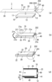
- FIG. 6C is an enlarged front view of a portion circled in FIG. 6B.
- 13A and 13B are equivalent circuit diagrams of an RF tag according to a second embodiment of the present invention
- 9(a) is a plan view showing the structure of an RF tag antenna according to a third embodiment
- FIG. 9(b) is an enlarged plan view of a portion circled in FIG. 9(a)
- 10(a) is a plan view showing the structure of an RF tag antenna according to a fourth embodiment
- FIG. 10(b) is an enlarged plan view of a portion circled in FIG.
- the RF tag antenna 1 includes an insulating substrate 10, a main waveguide element 20, a ground plate 30, a sub-waveguide element 40, a coating layer 70 made of an insulating material, and a frequency adjustment capacitor 203.
- the main waveguide element 20, the ground plate 30, and the sub-waveguide element 40 are formed on the surface of the coating layer 70.
- the RF tag 2 is configured by attaching an IC chip 60 to the RF tag antenna 1.
- the insulating substrate 10 has a surface 11, a back surface 12, and a side surface 13.
- the shape of the insulating substrate 10 is, for example, a substantially rectangular parallelepiped, but is not limited thereto and may be, for example, a disk-like or arc-shaped curved shape. It is preferable that the insulating substrate 10 has a shape that corresponds to the surface shape of the object to which the RF tag 2 is to be attached. For example, if the object is cylindrical and the RF tag 2 is to be attached to its curved surface, it is preferable that the shape of the RF tag 2 matches the curvature of the curved surface.
- the insulating substrate 10 may be made of polystyrene foam, polyethylene, polyimide, or the like. Furthermore, the insulating substrate 10 may be made of a dielectric material such as ceramic, paper, or resin.
- the main waveguide element 20 is provided on the surface 11 of the insulating substrate 10.
- the main waveguide element 20 of this embodiment has a rectangular shape, and is formed by a known method such as etching a thin metal film such as aluminum or pattern printing.
- the ground plane 30 is electrically connected to the main waveguide element 20 and is provided on the back surface 12 of the insulating substrate 10.
- the ground plane 30 in this embodiment has a rectangular shape, and is formed on the surface of the coating layer 70 by a known method such as etching a thin metal film of aluminum or the like, or pattern printing, in the same manner as the main waveguide element 20.
- the secondary waveguide element 40 is not directly (physically) connected to the primary waveguide element 20, that is, the edges are cut off.
- a protruding portion 41 is provided on a part of the side of the secondary waveguide element 40, and a protruding portion 23 is provided on a part of the side of the primary waveguide element 20.
- One terminal of the IC chip 60 is connected to the protruding portion 41, and the other terminal is connected to the protruding portion 23 of the primary waveguide element 20, so that the secondary waveguide element 40 and the primary waveguide element 20 are connected via the IC chip 60.
- both terminals of the IC chip 60 may be directly connected to the secondary waveguide element 40 and the primary waveguide element 20 without providing the protruding portions 23 and 41.
- the coating layer 70 is folded at the side of the insulating substrate 10 (see the arrow) and attached to the insulating substrate 10 via an adhesive layer (not shown).
- the auxiliary waveguide element 40 overlaps with the ground plate 30 via the coating layer 70, and the auxiliary waveguide element 40, the coating layer 70, and the ground plate 30 form a capacitor 80 (see FIG. 2).
- the main waveguide element 20, the base plate 30, and the secondary waveguide element 40 are formed on the surface of the coating layer 70, but the coating layer 70 need only be present at least in the portion where the secondary waveguide element 40 and the base plate 30 overlap.
- the resonant frequency can be adjusted by changing the area of the portion where the secondary waveguide element 40 overlaps with the base plate 30 via the coating layer 70.
- the material of the coating layer 70 is not particularly limited as long as it has flexibility and insulating properties, and may be, for example, PET, polyimide, vinyl, etc.
- the thickness of the coating layer 70 is not particularly limited, but is generally about several tens of ⁇ m.
- the main waveguide element 20, the ground plane 30 and the secondary waveguide element 40 surround the insulating substrate 10 in an annular shape.
- the main wave element 20 is preferably designed so that the total length L of its sides 21a to 21i is either ⁇ /4, ⁇ /2, 3 ⁇ /4, or 5 ⁇ /8. ⁇ is the wavelength of the radio waves transmitted from the reading device. In this embodiment, the length of the side is adjusted to be large by providing a notch 22 on the side of the main wave element 20.
- the main wave element 20 may be configured without the notch 22.
- the frequency adjustment capacitor 203 is provided between the primary waveguide element 20 and the secondary waveguide element 40 .
- the frequency adjusting capacitor 203 of this embodiment is composed of a frequency adjusting element 200 having an insulating layer 201 and a conductive layer 202 .
- the insulating layer 201 is made of an insulator and is placed between the main waveguide element 20 and the sub-guiding element 40.
- a conductive layer 202 is placed on the insulating layer 201.
- the conductive layer 202 needs to be long enough to overlap with the main waveguide element 20 and the sub-guiding element 40.
- the upper part of the insulating layer 201 is covered with the conductive layer 202, and a part of the lower part of the insulating layer 201 is covered with the main waveguide element 20 and the sub-guiding element 40, forming a frequency adjustment capacitor 203.
- the IC chip 60 operates based on the radio waves received by the RF tag antenna 1. Specifically, the IC chip 60 rectifies part of the carrier waves transmitted from the reader and generates the power supply voltage required for operation. The IC chip 60 then uses the generated power supply voltage to operate the control logic circuit within the IC chip 60 and the non-volatile memory that stores the product's unique information, and to operate communication circuits for sending and receiving data to and from the reader.
- a resonant circuit is configured to resonate in the frequency band of the received radio waves.
- This resonant circuit is configured with an inductor pattern, a capacitor 80, and an IC chip 60, as shown in the equivalent circuit diagram of Figure 3.
- the inductor pattern is configured with a primary waveguide element 20 and a ground plane 30.
- the primary waveguide element 20 and the secondary waveguide element 40 are connected by the equivalent capacitance of the IC chip 60.
- the capacitor 80 is composed of the sub-waveguide element 40, the coating layer 70 and the ground plane 30 as described above.
- Some IC chips 60 include a capacitor therein, and the IC chips 60 have stray capacitance. For this reason, when setting the resonant frequency of the resonant circuit, it is preferable to take into consideration the equivalent capacitance inside the IC chip 60. In other words, it is preferable for the resonant circuit to have a resonant frequency that is set in consideration of the inductance of the inductor pattern L, the capacitance of the capacitor 80, and the equivalent capacitance inside the IC chip 60.
- the resonant frequency f 0 [Hz] of this series resonant circuit is given by the following formula (1):
- the value of the resonant frequency f 0 is preferably set to be approximately the center value of the frequency bandwidth of the multiple radio waves transmitted from the reader.
- La is the inductance of the inductor pattern
- Ca is the capacitance of the capacitor 80
- Cb is the equivalent capacitance inside the IC chip 60. Note that, for example, a capacitance value published as one of the specifications of the IC chip 60 to be used can be used as Cb.
- the resonant frequency f0 of the resonant circuit can be set accurately to the frequency band of the radio wave.
- the reading performance of the RF tag 2 can be improved.
- the power supply voltage generated by the IC chip 60 can be increased.
- 3(b) shows a case where the area of the portion where the auxiliary waveguide element 40 overlaps with the ground plane 30 via the coating layer 70 is relatively large (see the circled area in FIG. 3(b)). In this way, by changing the area of the portion where the auxiliary waveguide element 40 overlaps with the ground plane 30 via the coating layer 70, it is possible to adjust Ca and thereby adjust the resonant frequency f0 .
- the inductance La can be increased by annularly surrounding the insulating substrate 10 with the primary waveguide element 20, the ground plate 30, and the secondary waveguide element 40.
- the resistance value increases, and the Q value of the series resonant circuit decreases based on the resistance value, resulting in a wider bandwidth and an RF tag antenna and an RF tag that can operate over a wide frequency band.
- the impedance becomes higher and the resonant frequency becomes lower. As a result, it becomes difficult to tune to the target resonant frequency f 0.
- the RF tag antenna 1 of the present invention is characterized in that it includes a frequency adjustment capacitor 203 (frequency adjustment element 200).
- a frequency adjustment capacitor 203 frequency adjustment element 200
- the main waveguide element 20 and the ground plane 30 constituting the inductor pattern L are also reduced in size.
- the frequency f0 in the above formula (1) becomes high, and there is a risk of it being outside the desired frequency band. Therefore, by providing a frequency adjustment capacitor 203 in a position parallel to the IC chip 60, the resonance frequency f 0 [Hz] is given by equation (2), and f 0 can be adjusted to a low value.
- La is the inductance of the inductor pattern L
- Ca is the capacitance of the capacitor 80
- Cb is the equivalent capacitance inside the IC chip 60
- Cc is the capacitance of the frequency adjustment capacitor 203.
- both ends of the short circuit are electrically connected to the first and second waveguide elements to form a planar inverted-F antenna (see FIG. 4C of Patent No. 6705116).
- an insulator layer 201 is placed across the primary waveguide element 20 and the secondary waveguide element 40, and a conductor layer 202 is placed on top of that.
- the conductor layer 202 is not electrically connected to the primary waveguide element 20 and the secondary waveguide element 40, and that the RF tag antenna 5 does not form a planar inverted-F antenna.
- Figure 4 is a graph showing the radio wave frequency (horizontal axis) and reading distance (vertical axis) of the RF tag antenna 1.
- the radio wave frequency horizontal axis
- reading distance vertical axis
- one RF tag 2 can be used for two frequency bands: the low frequency side (around 860 MHz) used mainly in Europe, and the high frequency side (around 920 MHz) used mainly in Japan.
- the RF tag 2 attached to the conductor 100 will be described with reference to FIGS.
- the RF tag 2 of the present invention can be used as it is, or can be used by contacting it with a conductor 100 .
- the back side of the RF tag 2 can be attached to the conductor 100 using an adhesive layer 101 made of an insulating material.
- the term "conductor” is a general term for a material with a relatively high electrical conductivity, similar to the general dictionary meaning, with metal being a typical example.
- the "conductor” is not limited to metal, and may be, for example, the human body, grass, trees, water, the ground, etc.
- a capacitor 81 with a coupling capacitance C is formed consisting of the ground plate 30, the sub-wave director element 40, the adhesive layer 101, and the conductor 100, so that the conductor 100 can be used as a director due to the capacitive coupling effect.
- the RF tag 2 can receive not only radio waves that reach the front side of the conductor 100, but also radio waves that reach the back side of the conductor 100.
- the "Conductor front” line in FIG. 4 shows the case where radio waves that reach the front side of the conductor 100 are read, and the "Conductor back” line shows the case where radio waves that reach the back side of the conductor 100 are read.
- the RF tag antenna 3 of this embodiment connects the secondary waveguide element 40 and the ground plate 30 via an IC chip 60. It is characterized in that at least a part of the secondary waveguide element 40 overlaps with the primary waveguide element 20 via a coating layer 70, so that a capacitor 82 is formed by the secondary waveguide element 40, the coating layer 70 and the primary waveguide element 20.
- the main waveguide element 20, the ground plane 30 and the secondary waveguide element 40 surround the insulating substrate 10 in an annular shape.
- the frequency adjustment capacitor 203 is provided between the ground plane 30 and the secondary director element 40. The resonant frequency can be adjusted by changing the area of the portion where the secondary director element 40 overlaps with the primary director element 20 via the coating layer 70.
- a resonant circuit is configured to resonate in the frequency band of the received radio waves.
- This resonant circuit is configured with an inductor pattern, a capacitor 82, a frequency adjustment capacitor 203, and an IC chip 60, as shown in the equivalent circuit diagram of Fig. 8.
- the inductor pattern is configured with a primary waveguide element 20 and a ground plate 30.
- the secondary waveguide element 40 and the ground plate 30 are connected through the equivalent capacitance of the IC chip 60.
- the capacitor 82 is comprised of the secondary waveguide element 40, the cladding layer 70 and the primary waveguide element 20 as described above.
- the inductance La is increased by annularly surrounding the insulating substrate 10 with the primary waveguide element 20, the ground plate 30, and the secondary waveguide element 40.
- the resistance value increases, and the Q value of the series resonant circuit decreases based on the resistance value, resulting in a wider bandwidth and an RF tag antenna 3 and an RF tag 4 that operate over a wide frequency band.
- 8(b) shows a case where the area of the portion where the secondary waveguide element 40 overlaps with the primary waveguide element 20 via the coating layer 70 is relatively large (see the circled area in FIG. 8(b)). In this way, by changing the area of the portion where the secondary waveguide element 40 overlaps with the primary waveguide element 20 via the coating layer 70, it is possible to adjust Ca in the above formula (2) and thereby adjust the resonant frequency f0 .
- FIG. 9 A third embodiment of an antenna for an RF tag and an RF tag according to the present invention will be described with reference to the drawings.
- the same reference numerals will be used to designate parts having the same configuration as those of the above-described embodiments, and the description thereof will be omitted.
- this embodiment is characterized in that the frequency adjustment capacitor 203 is composed of a first extension piece 204 extending from the end of the main waveguide element 20 toward the secondary waveguide element 40, a second extension piece 205 extending from the end of the secondary waveguide element 40 toward the main waveguide element 20 opposite the first extension piece 204, and a gap 206 formed between the tip of the first extension piece and the tip of the second extension piece.
- the first extension piece 204 is T-shaped and is composed of a base portion 204a extending from the end portion of the main waveguide element 20 toward the secondary waveguide element 40, and a tip portion 204b extending from the tip of the base portion 204a in a direction perpendicular to the base portion 204a.
- the second extension piece 205 is also T-shaped and is composed of a base portion 205a extending from the end portion of the secondary waveguide element 40 toward the primary waveguide element 20, and a tip portion 205b extending from the tip of the base portion 205a in a direction perpendicular to the base portion 205a.
- the two tip portions 204b, 205b are arranged in parallel with a gap 206 therebetween.
- the first extension piece and the second extension piece are formed by a known method such as etching a thin metal film such as aluminum or pattern printing.
- a capacitor is formed by the two tip portions 204b, 205b and the gap 206.
- the resonance frequency f 0 [Hz] is given by the above formula (2), and f 0 can be adjusted to a low value.
- the capacitance C C of the frequency adjustment capacitor 203 can be changed, and f 0 can be adjusted.
- the frequency adjustment capacitor is composed of an island piece 207 arranged in an island shape between the main waveguide element 20 and the secondary waveguide element 40, and gaps 208a to 208d formed between the island piece 207 and the main waveguide element 20 and between the island piece 207 and the secondary waveguide element 40.
- the island-like pieces 207 are formed by a known method such as etching a thin metal film such as aluminum or pattern printing.
- two island pieces 207 are arranged on either side of the IC chip 60 to form four gaps 208a to 208d, which results in four capacitors 209a to 209d being configured as frequency adjustment capacitors as shown in FIG. 11.
- the capacitance Cd of the frequency adjustment capacitor is given by equation (3).
- the resonance frequency f0 [Hz] is given by equation (4), and f0 can be adjusted to a low value.
- the capacitance Cd of the frequency adjustment capacitor can be changed to adjust f0 .
- Cd is the capacitance of the frequency adjustment capacitor
- C1 is the capacitance of capacitor 209a
- C2 is the capacitance of capacitor 209b
- C3 is the capacitance of capacitor 209c
- C4 is the capacitance of capacitor 209d.
- La is the inductance of the inductor pattern L
- Ca is the capacitance of the capacitor 80
- Cb is the equivalent capacitance inside the IC chip 60
- Cd is the capacitance of the frequency adjustment capacitor.
- FIG. 12(a) A fourth embodiment of the RF tag antenna and RF tag of the present invention will be described with reference to the drawings.
- the same reference numerals will be used to designate the same components as those of the above-described embodiments, and the description thereof will be omitted.
- an L-shaped slit 42 is provided in a part of the secondary waveguide element 40 to form a tongue-shaped piece 210, and the base of the tongue-shaped piece 210 is bent at the dotted line and joined to the back surface of the primary waveguide element 20 via an insulator to insulate the primary waveguide element 20 from the tongue-shaped piece 210 as shown in FIG. 12(b), to form a frequency adjustment capacitor.
- the frequency adjustment capacitor is composed of a primary waveguide element 20, a secondary waveguide element 40, a coating layer 70 made of an insulating material, and a tongue-shaped piece 210.
- a tongue-shaped piece may be formed by providing a slit in part of the main waveguide element 20, and the base of the tongue-shaped piece may be folded and joined to the back surface of the secondary waveguide element 40 via an insulator to insulate the secondary waveguide element 40 from the tongue-shaped piece, thereby forming a frequency adjustment capacitor.
- a tongue-shaped piece 210 may be formed by providing an L-shaped slit 42 in a part of the secondary waveguide element 40, and the base of the tongue-shaped piece 210 may be folded at the dotted line and joined to the rear surface of the base plate 30 via an insulator to insulate the base plate 30 from the tongue-shaped piece 210 as shown in FIG. 13(b), thereby forming a frequency adjustment capacitor.
- the frequency adjustment capacitor is composed of a ground plane 30, a sub-wave director element 40, a coating layer 70 made of an insulating material, and a tongue-shaped piece 210.
- a tongue-shaped piece may be formed by providing a slit in part of the base plate 30, and the base of the tongue-shaped piece may be bent and joined to the rear surface of the secondary waveguide element 40 to form a frequency adjustment capacitor.
- FIG. 14 shows a comprehensive list of modified examples of the RF tag antenna and RF tag of the present invention.
- FIG. 14( a ) shows a configuration in which the secondary director element 40 , the primary director element 20 , and the ground plane 30 are wrapped around the insulating substrate 10 with the coating layer 70 in contact with the insulating substrate 10 , and the surface of the secondary director element 40 is covered with part of the ground plane 30 .
- FIG. 14(b) shows a configuration in which the secondary waveguide element 40, the ground plane 30, and the main waveguide element 20 are wrapped around the insulating substrate 10 with the coating layer 70 in contact with the insulating substrate 10, and the surface of the secondary waveguide element 40 is covered with part of the main waveguide element 20.
- FIG. 14(c) shows a configuration in which the coating layer 70 is exposed to the outside, that is, turned upside down from the state shown in FIG. 1(a), the main waveguide element 20 and the ground plate 30 are wrapped around the insulating substrate 10, and part of the surface of the ground plate 30 is covered with the sub-guiding element 40.
- the IC chip 60 is not exposed to the outside, so the risk of damage can be reduced.
- FIG. 14( d ) shows a configuration in which the main waveguide element 20 and the ground plane 30 are wrapped around the insulating substrate 10 with the coating layer 70 exposed to the outside, and part of the surface of the main waveguide element 20 is covered with the secondary waveguide element 40 .
- FIG. 14( e ) shows a configuration in which the secondary waveguide element 40, the primary waveguide element 20 and the ground plate 30 are wrapped around an insulating substrate 10 with the coating layer 70 exposed to the outside, and the surface of the secondary waveguide element 40 is covered with part of the ground plate 30 .
- FIG. 14( f ) shows a configuration in which the secondary waveguide element 40, the ground plane 30, and the main waveguide element 20 are wrapped around the insulating substrate 10 with the coating layer 70 exposed to the outside, and the surface of the secondary waveguide element 40 is covered with part of the main waveguide element 20 .
- an RF tag antenna and an RF tag that operate in a wide frequency band can be obtained.
- a frequency adjustment capacitor is provided in any of the configurations shown in Figures 14(a) to (f).
- the present invention is an antenna for RF tags and an RF tag that operate over a wide frequency band, and has industrial applicability.
- RF tag antenna 1.
- RF tag antenna 2.
- RF tag 3. RF tag antenna 4.
- RF Tag 10 Insulating substrate 11 Surface 12 Back 13 Side 20 Main Wave Element 21a to 21i Side 22 Cut 23 Convex 30 Main plate 40
- Sub-waveguide element 41
- Convex 42 Slit 60
- IC chips 70
- Coating Layer 80
- Capacitor 81 Capacitor 82
- Conductor 101 Adhesive layer
- Frequency Adjustment Element 201
- Conductive layer 203
- Frequency adjustment capacitor 204 First extension piece 204a Base 204b Tip 205 2nd extension piece 205a
- Base 205b Tip 206 Gap 207 Island 208a to 208d Gap 209a to 209d
Landscapes
- Engineering & Computer Science (AREA)
- Computer Hardware Design (AREA)
- Microelectronics & Electronic Packaging (AREA)
- Physics & Mathematics (AREA)
- General Physics & Mathematics (AREA)
- Theoretical Computer Science (AREA)
- Waveguide Aerials (AREA)
Abstract
広い周波数帯域で動作するRFタグ用アンテナ及びRFタグを提供する。 本発明のRFタグ用アンテナ1は、絶縁基材10と、主導波素子20と、主導波素子と電気的に接続される地板30と、主導波素子とICチップ60を介して接続される副導波素子40と、周波数調整用コンデンサ203とを備える。副導波素子の少なくとも一部が絶縁材からなる被膜層70を介して地板と重なることにより副導波素子、被膜層及び地板によってコンデンサを形成すると共に、主導波素子、地板及び副導波素子によって絶縁基材を環状に取り囲む。周波数調整用コンデンサは主導波素子と副導波素子の間に設けられる。絶縁基材を環状に取り囲むことでインダクタンスが大きくなり、抵抗値が大きくなり、直列共振回路のQ値が低下する。その結果、帯域幅が広くなり、広い周波数帯域で動作するRFタグ用アンテナ及びRFタグを得られる。
Description
本発明は、広い周波数帯域で動作するRFタグ用アンテナ及びRFタグに関する。
RFID(Radio Frequency Identification)システムで使用するRFタグにはアンテナ及びRFチップ(ICチップ)が格納されており、リーダ・ライタのアンテナから送信された搬送波をアンテナで受信し、RFチップに記録されている識別データ等を反射波に乗せてリーダ・ライタへ返送することにより、非接触で交信する仕組みになっている。
RFタグは広い周波数帯域で動作することが求められる場合がある。
例えば特許文献1のデュアルRFタグは、表面にローバンド放射エレメント部、ハイバンド放射エレメント部、インダクタパターン部、バランスコイル部及びICチップを備えており、裏面にグランドエレメント部を備えており、表面と裏面の間に絶縁基材を備えており、グランドエレメント部とバランスコイル部を電気的に導通させている。
そして、バランスコイル部の一次側コイルの一方の端部にローバンド放射エレメント部、他方の端部にハイバンド放射エレメント部を接続し、一次側コイルの中間点にグランドエレメントを接続している。一次側コイルの中間点にグランドエレメントを接続していることから、一次側コイルの一方の端部から中間点までが第1コイル、一次側コイルの他方の端部から中間点までが第2コイルとなる二つのコイル構成となる。ローバンド放射エレメント部が低周波数用、ハイバンド放射エレメント部が高周波数用のアンテナとして機能することで、ローバンドとハイバンドをスイッチ機構で切り替えることなく、2種類の周波数帯域で動作する。
また、特許文献2のデュアルRFタグは、絶縁基材、主導波素子、副導波素子、地板、給電部及び短絡部により板状逆Fアンテナを構成する。そして、副導波素子の位置を変更して、副導波素子と主導波素子が対向する部分の面積を変更することにより、電波の波長λを低周波数側と高周波数側に切り替えることができる。
上記特許文献1の技術は一次側コイルとして第1コイル及び第2コイルの二つのコイル構成にしているが、仮に一時側コイルとして一方の端部から他方の端部までを一つのコイル構成にする場合と比較すると、特許文献1の構成の場合はバランスコイルの二次側コイルとの送受信電力が1/2になってしまう。このように、ローバンドとハイバンドとを切り替えるためのスイッチ機構を備えずに2種類の周波数帯域で動作させる場合には送受信電力が1/2に減少してしまい、通信距離が短くなるという問題がある。
特許文献2の技術は副導波素子の位置を変更して低周波数側と高周波数側に切り替える必要があるため、変更作業に手間がかかるという問題や製造コストが嵩むという問題がある。
特許文献2の技術は副導波素子の位置を変更して低周波数側と高周波数側に切り替える必要があるため、変更作業に手間がかかるという問題や製造コストが嵩むという問題がある。
本発明はこのような問題を考慮して、広い周波数帯域で動作するRFタグ用アンテナ及びRFタグを提供することを目的とする。
本発明のRFタグ用アンテナは、絶縁基材と、主導波素子と、前記主導波素子と電気的に接続される地板と、前記主導波素子とICチップを介して接続される副導波素子と、周波数調整用コンデンサとを備えており、前記主導波素子は前記絶縁基材の表面に設けられ、前記地板は前記絶縁基材の裏面に設けられるものであり、前記副導波素子の少なくとも一部が絶縁材からなる被膜層を介して前記地板と重なることにより前記副導波素子、前記被膜層及び前記地板によってコンデンサを形成すると共に、前記主導波素子、前記地板及び前記副導波素子によって前記絶縁基材を環状に取り囲むものであり、前記周波数調整用コンデンサは前記主導波素子と前記副導波素子の間に設けられることを特徴とする。
また、前記周波数調整用コンデンサが、絶縁体層と導電体層から成る周波数調整用エレメントで構成され、前記絶縁体層は前記主導波素子と前記副導波素子との間に掛け渡され、前記絶縁体層の上に前記導電体層が配置されることを特徴とする。
また、前記周波数調整用コンデンサが、絶縁体層と導電体層から成る周波数調整用エレメントで構成され、前記絶縁体層は前記主導波素子と前記副導波素子との間に掛け渡され、前記絶縁体層の上に前記導電体層が配置されることを特徴とする。
また、前記周波数調整用コンデンサが、前記主導波素子の端部から前記副導波素子側にのびる第1延長片と、前記第1延長片に対向して前記副導波素子の端部から前記主導波素子側にのびる第2延長片と、前記第1延長片の先端と前記第2延長片の先端の間に形成される隙間で構成されることを特徴とする。
また、前記周波数調整用コンデンサが、前記主導波素子と前記副導波素子との間に島状に配置される島状片と、前記島状片と前記主導波素子及び前記副導波素子の間に形成される隙間で構成されることを特徴とする。
また、前記周波数調整用コンデンサが、前記主導波素子と前記副導波素子との間に島状に配置される島状片と、前記島状片と前記主導波素子及び前記副導波素子の間に形成される隙間で構成されることを特徴とする。
また、絶縁基材と、主導波素子と、前記主導波素子と電気的に接続される地板と、前記地板とICチップを介して接続される副導波素子と、周波数調整用コンデンサとを備えており、前記主導波素子は前記絶縁基材の表面に設けられ、前記地板は前記絶縁基材の裏面に設けられるものであり、前記副導波素子の少なくとも一部が絶縁材からなる被膜層を介して前記主導波素子と重なることにより前記副導波素子、前記被膜層及び前記主導波素子によってコンデンサを形成すると共に、前記主導波素子、前記地板及び前記副導波素子によって前記絶縁基材を環状に取り囲むものであり、前記周波数調整用コンデンサは前記地板と前記副導波素子の間に設けられることを特徴とする。
また、前記周波数調整用コンデンサが、絶縁体層と導電体層から成る周波数調整用エレメントで構成され、前記絶縁体層は前記地板と前記副導波素子との間に掛け渡され、前記絶縁体層の上に前記導電体層が配置されることを特徴とする。
また、前記周波数調整用コンデンサが、絶縁体層と導電体層から成る周波数調整用エレメントで構成され、前記絶縁体層は前記地板と前記副導波素子との間に掛け渡され、前記絶縁体層の上に前記導電体層が配置されることを特徴とする。
また、前記周波数調整用コンデンサが、前記地板の端部から前記副導波素子側にのびる第1延長片と、前記第1延長片に対向して前記副導波素子の端部から前記主導波素子側にのびる第2延長片と、前記第1延長片の先端と前記第2延長片の先端の間に形成される隙間で構成されることを特徴とする。
また、前記周波数調整用コンデンサが、前記地板と前記副導波素子との間に島状に配置される島状片と、前記島状片と前記地板及び/又は前記副導波素子の間に形成される隙間で構成されることを特徴とする。
また、絶縁材からなる粘着層を備えることを特徴とする。
また、前記主導波素子の側辺に切り込みを備えることを特徴とする。
また、前記周波数調整用コンデンサが、前記地板と前記副導波素子との間に島状に配置される島状片と、前記島状片と前記地板及び/又は前記副導波素子の間に形成される隙間で構成されることを特徴とする。
また、絶縁材からなる粘着層を備えることを特徴とする。
また、前記主導波素子の側辺に切り込みを備えることを特徴とする。
本発明のRFタグは、上記RFタグ用アンテナと、前記ICチップと、前記電波の周波数帯域で共振する共振回路を備えており、前記共振回路は前記主導波素子及び前記地板により構成されるインダクタパターン、前記コンデンサ及び前記ICチップにより構成されることを特徴とする。
本発明では主導波素子、地板及び副導波素子によって絶縁基材を環状に取り囲むことでインダクタンスLaを大きくする。誘導性リアクタンスXL=2πfLaの式において抵抗値が大きくなるので、抵抗値に基づいて直列共振回路のQ値が低下する結果、帯域幅が広くなり、広い周波数帯域で動作するRFタグ用アンテナ及びRFタグを得られる。
また、周波数調整用コンデンサをICチップと平行する位置に設けることでf0を低い値に調節することができる。
また、周波数調整用コンデンサをICチップと平行する位置に設けることでf0を低い値に調節することができる。
また、副導波素子が被膜層を介して地板と重なっている部分の面積を変えることでコンデンサの静電容量を調節して共振周波数を調節することができる。
絶縁材からなる粘着層を用いてRFタグを導体に貼り付けることができる。この場合、地板及び副導波素子、粘着層、導体からなる結合容量コンデンサが形成されるので、静電容量結合効果により導体を導波器として利用することができる。
主導波素子の側縁に切り込みを設けることで読取装置から送信されて主導波素子で受信する電波の波長を調節できる。
絶縁材からなる粘着層を用いてRFタグを導体に貼り付けることができる。この場合、地板及び副導波素子、粘着層、導体からなる結合容量コンデンサが形成されるので、静電容量結合効果により導体を導波器として利用することができる。
主導波素子の側縁に切り込みを設けることで読取装置から送信されて主導波素子で受信する電波の波長を調節できる。
[第1の実施の形態]
本発明のRFタグ用アンテナ及びRFタグの第1の実施の形態について図面を用いて説明する。
図1及び図2に示すようにRFタグ用アンテナ1は絶縁基材10、主導波素子20、地板30、副導波素子40、絶縁材からなる被膜層70、周波数調整用コンデンサ203を備えている。主導波素子20、地板30及び副導波素子40は被膜層70の表面に形成される。RFタグ2はRFタグ用アンテナ1にICチップ60を取り付けて構成される。
本発明のRFタグ用アンテナ及びRFタグの第1の実施の形態について図面を用いて説明する。
図1及び図2に示すようにRFタグ用アンテナ1は絶縁基材10、主導波素子20、地板30、副導波素子40、絶縁材からなる被膜層70、周波数調整用コンデンサ203を備えている。主導波素子20、地板30及び副導波素子40は被膜層70の表面に形成される。RFタグ2はRFタグ用アンテナ1にICチップ60を取り付けて構成される。
絶縁基材10は表面11、裏面12及び側面13を有する。絶縁基材10の形状は例えば略直方体であるが、これに限らず例えば円盤状や円弧状に湾曲したものであってもよい。絶縁基材10はRFタグ2が取り付けられる被取付物の表面形状に応じた形状を有するのが好ましい。例えば被取付物が円筒形状であってその湾曲面にRFタグ2を取り付ける場合には、RFタグ2の形状を湾曲面の曲率に合わせるのが好ましい。絶縁基材10としては発泡スチロール、ポリエチレン、ポリイミド等を用いればよい。また、絶縁基材10としてセラミック、紙、樹脂等の誘電体を用いてもよい。
主導波素子20は絶縁基材10の表面11に設けられる。本実施の形態の主導波素子20は長方形状であり、アルミ等の金属薄膜のエッチングやパターン印刷等の周知の手法によって形成される。
地板30は主導波素子20と電気的に接続されており、絶縁基材10の裏面12に設けられる。本実施の形態の地板30は長方形状であり、主導波素子20と同様にアルミ等の金属薄膜のエッチングやパターン印刷等の周知の手法によって被膜層70の表面に形成される。
地板30は主導波素子20と電気的に接続されており、絶縁基材10の裏面12に設けられる。本実施の形態の地板30は長方形状であり、主導波素子20と同様にアルミ等の金属薄膜のエッチングやパターン印刷等の周知の手法によって被膜層70の表面に形成される。
図1(a)及び(d)に示すように副導波素子40は主導波素子20と直接的(物理的)に繋がっていない、つまり縁が切れた状態である。副導波素子40の側辺の一部に凸部41を設け、主導波素子20の側辺の一部に凸部23を設けてある。ICチップ60の一方の端子を凸部41に接続し、他方の端子を主導波素子20の凸部23に接続することで副導波素子40と主導波素子20とはICチップ60を介して接続される。なお、凸部23,41を設けずにICチップ60の両端子を直接副導波素子40及び主導波素子20に接続してもよい。
図1(b)に示すように被膜層70を絶縁基材10の辺の部分で折り曲げて(矢印参照)、図示しない粘着層を介して絶縁基材10に貼り付けている。これにより図1(c)及び(d)に示すように副導波素子40は少なくともその一部が被膜層70を介して地板30と重なることになり、副導波素子40、被膜層70及び地板30によってコンデンサ80(図2参照)が形成される。
図1(b)に示すように被膜層70を絶縁基材10の辺の部分で折り曲げて(矢印参照)、図示しない粘着層を介して絶縁基材10に貼り付けている。これにより図1(c)及び(d)に示すように副導波素子40は少なくともその一部が被膜層70を介して地板30と重なることになり、副導波素子40、被膜層70及び地板30によってコンデンサ80(図2参照)が形成される。
本実施の形態では被膜層70の表面に主導波素子20、地板30及び副導波素子40を形成しているが、被膜層70は少なくとも副導波素子40と地板30とが重なっている部分に存在すればよい。詳しい説明は後述するが、副導波素子40が被膜層70を介して地板30と重なっている部分の面積を変えることで共振周波数を調節することができる。
被膜層70の材料としては可撓性及び絶縁性を備えていれば特に限定されないが、例えばPET、ポリイミド、ビニールなどを用いればよい。被膜層70の厚さは特に限定されるものではないが一般的には数十μm程度である。
主導波素子20、地板30及び副導波素子40によって絶縁基材10を環状に取り囲んでいる。
被膜層70の材料としては可撓性及び絶縁性を備えていれば特に限定されないが、例えばPET、ポリイミド、ビニールなどを用いればよい。被膜層70の厚さは特に限定されるものではないが一般的には数十μm程度である。
主導波素子20、地板30及び副導波素子40によって絶縁基材10を環状に取り囲んでいる。
主導波素子20はその側辺21a~21iの長さの合計Lがλ/4、λ/2、3λ/4、5λ/8のいずれかになるように設計するのが好ましい。λは読取装置から送信される電波の波長である。本実施の形態では主導波素子20の側辺に切り込み22を設けることで側辺の長さが大きくなるように調節している。主導波素子20が切り込み22を備えない構成でも良い。
周波数調整用コンデンサ203は主導波素子20と副導波素子40の間に設けられる。
本実施の形態の周波数調整用コンデンサ203は絶縁体層201と導電体層202を備える周波数調整用エレメント200で構成される。
絶縁体層201は絶縁体から成り、主導波素子20と副導波素子40との間に掛け渡される。絶縁体層201の上に導電体層202が配置される。導電体層202は主導波素子20及び副導波素子40と重なる程度の長さにする必要がある。これにより、絶縁体層201の上部を導電体層202で覆い、絶縁体層201の下部の一部を主導波素子20及び副導波素子40で覆うことになり、周波数調整用コンデンサ203が形成される。
本実施の形態の周波数調整用コンデンサ203は絶縁体層201と導電体層202を備える周波数調整用エレメント200で構成される。
絶縁体層201は絶縁体から成り、主導波素子20と副導波素子40との間に掛け渡される。絶縁体層201の上に導電体層202が配置される。導電体層202は主導波素子20及び副導波素子40と重なる程度の長さにする必要がある。これにより、絶縁体層201の上部を導電体層202で覆い、絶縁体層201の下部の一部を主導波素子20及び副導波素子40で覆うことになり、周波数調整用コンデンサ203が形成される。
ICチップ60はRFタグ用アンテナ1が受信した電波に基づいて動作する。具体的にはICチップ60は読取装置から送信される搬送波の一部を整流し、動作に必要な電源電圧を生成する。そしてICチップ60は生成した電源電圧によって、ICチップ60内の制御用の論理回路や商品の固有情報等が格納された不揮発性メモリを動作させ、読取装置との間でデータの送受信を行うための通信回路等を動作させる。
次に、周波数調整用コンデンサ203を備えない場合のRFタグ用アンテナの構成、つまり図1の構成から周波数調整用コンデンサ203を削除したRFタグ用アンテナの構成について説明する。
周波数調整用コンデンサ203を備えないRFタグ用アンテナでは受信する電波の周波数帯域で共振するように共振回路を構成する。この共振回路は図3の等価回路図に示すようにインダクタパターン、コンデンサ80及びICチップ60により構成される。インダクタパターンは主導波素子20及び地板30で構成される。主導波素子20と副導波素子40とはICチップ60の等価容量で接続されることになる。
コンデンサ80は上述の通り副導波素子40、被膜層70及び地板30により構成される。
周波数調整用コンデンサ203を備えないRFタグ用アンテナでは受信する電波の周波数帯域で共振するように共振回路を構成する。この共振回路は図3の等価回路図に示すようにインダクタパターン、コンデンサ80及びICチップ60により構成される。インダクタパターンは主導波素子20及び地板30で構成される。主導波素子20と副導波素子40とはICチップ60の等価容量で接続されることになる。
コンデンサ80は上述の通り副導波素子40、被膜層70及び地板30により構成される。
ICチップ60には内部にコンデンサを含むものがあり、また、ICチップ60は浮遊容量を有する。このため、共振回路の共振周波数を設定する際、ICチップ60内部の等価容量を考慮することが好ましい。換言すれば、共振回路はインダクタパターンLのインダクタンス、コンデンサ80の静電容量及びICチップ60内部の等価容量を考慮して設定された共振周波数を有することが好ましい。
この直列共振回路の共振周波数f0[Hz]は、式(1)により与えられる。共振周波数f0の値は、読取装置から送信される複数の電波の周波数帯域幅のほぼ中心値になるように設定するのが好ましい。

ここで、La:インダクタパターンのインダクタンス、Ca: コンデンサ80の静電容量、Cb:ICチップ60内部の等価容量である。なお、Cbとしては例えば使用するICチップ60の仕様諸元の一つとして公表されている静電容量値を用いることができる。
この直列共振回路の共振周波数f0[Hz]は、式(1)により与えられる。共振周波数f0の値は、読取装置から送信される複数の電波の周波数帯域幅のほぼ中心値になるように設定するのが好ましい。
このようにICチップ60内部の等価容量を考慮することで、共振回路の共振周波数f0を電波の周波数帯域に精度良く設定することができる。その結果、RFタグ2の読み取り性能を向上させることができる。また、ICチップ60が生成する電源電圧を高くすることができる。
図3(a)と比較して図3(b)は副導波素子40が被膜層70を介して地板30と重なっている部分の面積が相対的に大きい場合を示している(図3(b)中の丸で囲んだ箇所を参照)。このように副導波素子40が被膜層70を介して地板30と重なっている部分の面積を変えることでCaを調節して共振周波数f0を調節することができる。
図3(a)と比較して図3(b)は副導波素子40が被膜層70を介して地板30と重なっている部分の面積が相対的に大きい場合を示している(図3(b)中の丸で囲んだ箇所を参照)。このように副導波素子40が被膜層70を介して地板30と重なっている部分の面積を変えることでCaを調節して共振周波数f0を調節することができる。
また、周波数調整用コンデンサ203を備えないRFタグ用アンテナでは主導波素子20、地板30及び副導波素子40によって絶縁基材10を環状に取り囲むことでインダクタンスLaを大きくできる。誘導性リアクタンスXL=2πfLaの式において抵抗値が大きくなり、抵抗値に基づいて直列共振回路のQ値が低下する結果、帯域幅が広くなり、広い周波数帯域で動作するRFタグ用アンテナ及びRFタグを得られる。
なお、インダクタンスLaを大きくしたことでインピーダンスが高くなり、共振周波数は低くなる。その結果、目標とする共振周波数f0に同調させるのが難しくなる。しかし、コンデンサ80の静電容量CaとICチップ60内の等価容量Cbとを結合した容量Cを設定することで、C=1/Ca + 1/Cbになるのでキャパシタンス容量が小さくなり、目標とする共振周波数f0に同調させることが可能になる。
なお、インダクタンスLaを大きくしたことでインピーダンスが高くなり、共振周波数は低くなる。その結果、目標とする共振周波数f0に同調させるのが難しくなる。しかし、コンデンサ80の静電容量CaとICチップ60内の等価容量Cbとを結合した容量Cを設定することで、C=1/Ca + 1/Cbになるのでキャパシタンス容量が小さくなり、目標とする共振周波数f0に同調させることが可能になる。
そして、図1及び図2に示すように本発明のRFタグ用アンテナ1は周波数調整用コンデンサ203(周波数調整用エレメント200)を備える点が特徴である。
RFタグを小型化するべく絶縁基材10の寸法を小さくする場合、インダクタパターンLを構成する主導波素子20及び地板30も小さくなる。その結果、上記式(1)において周波数f0が高くなってしまい、希望する周波数帯域から外れてしまうおそれがある。
そこで、ICチップ60と平行する位置に周波数調整用コンデンサ203を設けることで共振周波数f0[Hz]は式(2)により与えられることになり、f0を低い値に調節することができる。

ここで、La: インダクタパターンLのインダクタンス、Ca: コンデンサ80の静電容量、Cb:ICチップ60内部の等価容量、Cc:周波数調整用コンデンサ203の静電容量である。
RFタグを小型化するべく絶縁基材10の寸法を小さくする場合、インダクタパターンLを構成する主導波素子20及び地板30も小さくなる。その結果、上記式(1)において周波数f0が高くなってしまい、希望する周波数帯域から外れてしまうおそれがある。
そこで、ICチップ60と平行する位置に周波数調整用コンデンサ203を設けることで共振周波数f0[Hz]は式(2)により与えられることになり、f0を低い値に調節することができる。
なお、本願出願人の特許第6705116号では短絡部の両端を第1導波素子と第2導波素子に電気的に接続することで板状逆Fアンテナを構成している(特許第6705116号の図4C参照)。一方、本実施の形態のRFタグ用アンテナ5では主導波素子20と副導波素子40に絶縁体層201を掛け渡しておき、その上に導電体層202を配置している。つまり、導電体層202を主導波素子20と副導波素子40に電気的に接続しているわけではなく、RFタグ用アンテナ5は板状逆Fアンテナを構成していない点に注意を要する。
図4はRFタグ用アンテナ1の電波の周波数(横軸)と読取距離(縦軸)を示すグラフであり、Q値を低下させて帯域幅を広げた結果、主にヨーロッパで使用する低周波数側(860MHz付近)と主に日本で使用する高周波数側(920MHz付近)の2種類の周波数帯域に1つのRFタグ2で対応できているのが分かる。
図5及び図6を参照して導体100に設置したRFタグ2について説明する。
本発明のRFタグ2はそのまま使用できるし、導体100に接触させても使用できる。
具体的には、RFタグ2の裏面側を絶縁材からなる粘着層101を用いて導体100に貼り付けることができる。本願において「導体」とは、一般的な辞書的意味と同様に「電気の伝導率が比較的大きな物質の総称」であり、金属が典型的な例である。ただし、「導体」は金属に限定されるものではなく、例えば人体、草、木、水、地面などであってもよい。
本発明のRFタグ2はそのまま使用できるし、導体100に接触させても使用できる。
具体的には、RFタグ2の裏面側を絶縁材からなる粘着層101を用いて導体100に貼り付けることができる。本願において「導体」とは、一般的な辞書的意味と同様に「電気の伝導率が比較的大きな物質の総称」であり、金属が典型的な例である。ただし、「導体」は金属に限定されるものではなく、例えば人体、草、木、水、地面などであってもよい。
RFタグ2を粘着層101を用いて導体100に貼り付けることにより、地板30及び副導波素子40、粘着層101、導体100からなる結合容量Cのコンデンサ81が形成されるので、静電容量結合効果により導体100を導波器として利用することができる。この場合、図5に示すように導体100の表面側に到達した電波のみならず、導体100の裏面側に到達した電波もRFタグ2で受信することができる。図4中の「導体表」のラインは導体100の表面側に到達した電波を読み取った場合であり、「導体裏」のラインは導体100の裏面側に到達した電波を読み取った場合を示している。
[第2の実施の形態]
本発明のRFタグ用アンテナ及びRFタグの第2の実施の形態について図面を用いて説明するが、上記第1の実施の形態と同一の構成になる箇所については同一の符号を付してその説明を省略する。
図7及び図8に示すように本実施の形態のRFタグ用アンテナ3はICチップ60を介して副導波素子40と地板30とを接続するものである。副導波素子40の少なくとも一部が被膜層70を介して主導波素子20と重なることにより副導波素子40、被膜層70及び主導波素子20によってコンデンサ82を形成する点に特徴を有する。
主導波素子20、地板30及び副導波素子40によって絶縁基材10を環状に取り囲んでいる。
周波数調整用コンデンサ203は地板30と副導波素子40の間に設けられる
副導波素子40が被膜層70を介して主導波素子20と重なっている部分の面積を変えることで共振周波数を調節することができる。
RFタグ用アンテナ3では受信する電波の周波数帯域で共振するように共振回路を構成する。この共振回路は図8の等価回路図に示すようにインダクタパターン、コンデンサ82、周波数調整用コンデンサ203及びICチップ60により構成される。インダクタパターンは主導波素子20及び地板30で構成される。副導波素子40と地板30とはICチップ60の等価容量で接続されることになる。
コンデンサ82は上述の通り副導波素子40、被膜層70及び主導波素子20により構成される。
コンデンサ82は上述の通り副導波素子40、被膜層70及び主導波素子20により構成される。
本発明では主導波素子20、地板30及び副導波素子40によって絶縁基材10を環状に取り囲むことでインダクタンスLaを大きくしている。誘導性リアクタンスXL=2πfLaの式において抵抗値が大きくなり、抵抗値に基づいて直列共振回路のQ値が低下する結果、帯域幅が広くなり、広い周波数帯域で動作するRFタグ用アンテナ3及びRFタグ4を得られる。
図8(a)と比較して図8(b)は副導波素子40が被膜層70を介して主導波素子20と重なっている部分の面積が相対的に大きい場合を示している(図8(b)中の丸で囲んだ箇所を参照)。このように副導波素子40が被膜層70を介して主導波素子20と重なっている部分の面積を変えることで上記式(2)におけるCaを調節して共振周波数f0を調節することができる。
図8(a)と比較して図8(b)は副導波素子40が被膜層70を介して主導波素子20と重なっている部分の面積が相対的に大きい場合を示している(図8(b)中の丸で囲んだ箇所を参照)。このように副導波素子40が被膜層70を介して主導波素子20と重なっている部分の面積を変えることで上記式(2)におけるCaを調節して共振周波数f0を調節することができる。
[第3の実施の形態]
本発明のRFタグ用アンテナ及びRFタグの第3の実施の形態について図面を用いて説明するが、上記各実施の形態と同一の構成になる箇所については同一の符号を付してその説明を省略する。
図9に示すように本実施の形態では周波数調整用コンデンサ203が、主導波素子20の端部から副導波素子40側にのびる第1延長片204と、第1延長片204に対向して副導波素子40の端部から主導波素子20側にのびる第2延長片205と、第1延長片の先端と第2延長片の先端の間に形成される隙間206で構成される点が特徴である。
本発明のRFタグ用アンテナ及びRFタグの第3の実施の形態について図面を用いて説明するが、上記各実施の形態と同一の構成になる箇所については同一の符号を付してその説明を省略する。
図9に示すように本実施の形態では周波数調整用コンデンサ203が、主導波素子20の端部から副導波素子40側にのびる第1延長片204と、第1延長片204に対向して副導波素子40の端部から主導波素子20側にのびる第2延長片205と、第1延長片の先端と第2延長片の先端の間に形成される隙間206で構成される点が特徴である。
具体的には第1延長片204はT次状であり、主導波素子20の端部から副導波素子40側にのびる基部204aと、基部204aの先端から基部204aと直交する方向にのびる先端部204bで構成される。
第2延長片205もT次状であり、副導波素子40の端部から主導波素子20側にのびる基部205aと、基部205aの先端から基部205aと直交する方向にのびる先端部205bで構成される。2つの先端部204b,205bは隙間206を空けて平行に配置される。
第1延長片及び第2延長片はアルミ等の金属薄膜のエッチングやパターン印刷等の周知の手法によって形成される。
2つの先端部204b,205bと隙間206によってコンデンサが構成される。ICチップ60と平行する位置に周波数調整用コンデンサを設けることで共振周波数f0[Hz]は上記式(2)により与えられることになり、f0を低い値に調節することができる。また、先端部204b,205bの長さ及び隙間206の幅を変えることで周波数調整用コンデンサ203の静電容量CCを変化させてf0を調節することができる。
[第4の実施の形態]
本発明のRFタグ用アンテナ及びRFタグの第4の実施の形態について図面を用いて説明するが、上記各実施の形態と同一の構成になる箇所については同一の符号を付してその説明を省略する。
図10に示すように本実施の形態では周波数調整用コンデンサが、主導波素子20と副導波素子40との間に島状に配置される島状片207と、島状片207と主導波素子20及び副導波素子40の間に形成される隙間208a~208dで構成される点が特徴である。
島状片207はアルミ等の金属薄膜のエッチングやパターン印刷等の周知の手法によって形成される。
本発明のRFタグ用アンテナ及びRFタグの第4の実施の形態について図面を用いて説明するが、上記各実施の形態と同一の構成になる箇所については同一の符号を付してその説明を省略する。
図10に示すように本実施の形態では周波数調整用コンデンサが、主導波素子20と副導波素子40との間に島状に配置される島状片207と、島状片207と主導波素子20及び副導波素子40の間に形成される隙間208a~208dで構成される点が特徴である。
島状片207はアルミ等の金属薄膜のエッチングやパターン印刷等の周知の手法によって形成される。
本実施の形態ではICチップ60を挟んで2つの島状片207を配置することにより4つの隙間208a~208dを形成しており、これにより図11に示すように周波数調整用コンデンサとして4つのコンデンサ209a~209dが構成される。この場合、周波数調整用コンデンサの静電容量Cdは式(3)により与えられる。ICチップ60と平行する位置に周波数調整用コンデンサを設けることで共振周波数f0[Hz]は式(4)により与えられることになり、f0を低い値に調節することができる。また、島状片207の長さ及び幅、隙間208a~208dの幅を変えることで周波数調整用コンデンサの静電容量Cdを変化させてf0を調節することができる。
なお、島状片207を1つだけ配置してもよく、或いは3つ以上配置してもよい。

ここで、Cd:周波数調整用コンデンサの静電容量、C1:コンデンサ209aの静電容量、C2:コンデンサ209bの静電容量、C3:コンデンサ209cの静電容量、C4:コンデンサ209dの静電容量である。

ここで、La:インダクタパターンLのインダクタンス、Ca:コンデンサ80の静電容量、Cb:ICチップ60内部の等価容量、Cd:周波数調整用コンデンサの静電容量である。
なお、島状片207を1つだけ配置してもよく、或いは3つ以上配置してもよい。
[第5の実施の形態]
本発明のRFタグ用アンテナ及びRFタグの第4の実施の形態について図面を用いて説明するが、上記各実施の形態と同一の構成になる箇所については同一の符号を付してその説明を省略する。
図12(a)に示すように本実施の形態では副導波素子40の一部にL字状のスリット42を設けることで舌状片210を形成し、舌状片210の基部を点線箇所で折り曲げて図12(b)に示すように主導波素子20の裏面に、主導波素子20と舌状片210を絶縁するための絶縁体を介して接合することで周波数調整用コンデンサとする。
周波数調整用コンデンサは主導波素子20、副導波素子40、絶縁材からなる被膜層70、舌状片210で構成される。
本発明のRFタグ用アンテナ及びRFタグの第4の実施の形態について図面を用いて説明するが、上記各実施の形態と同一の構成になる箇所については同一の符号を付してその説明を省略する。
図12(a)に示すように本実施の形態では副導波素子40の一部にL字状のスリット42を設けることで舌状片210を形成し、舌状片210の基部を点線箇所で折り曲げて図12(b)に示すように主導波素子20の裏面に、主導波素子20と舌状片210を絶縁するための絶縁体を介して接合することで周波数調整用コンデンサとする。
周波数調整用コンデンサは主導波素子20、副導波素子40、絶縁材からなる被膜層70、舌状片210で構成される。
また、図示は省略するが主導波素子20の一部にスリットを設けることで舌状片を形成し、舌状片の基部を折り曲げて副導波素子40の裏面に、副導波素子40と舌状片を絶縁するための絶縁体を介して接合することで周波数調整用コンデンサとしてもよい。
また、図13(a)に示すように副導波素子40の一部にL字状のスリット42を設けることで舌状片210を形成し、舌状片210の基部を点線箇所で折り曲げて図13(b)に示すように地板30の裏面に、地板30と舌状片210を絶縁するための絶縁体を介して接合することで周波数調整用コンデンサとしてもよい。
周波数調整用コンデンサは地板30、副導波素子40、絶縁材からなる被膜層70、舌状片210で構成される。
また、地板30の一部にスリットを設けることで舌状片を形成し、舌状片の基部を折り曲げて副導波素子40の裏面に接合することで周波数調整用コンデンサとしてもよい。
また、図13(a)に示すように副導波素子40の一部にL字状のスリット42を設けることで舌状片210を形成し、舌状片210の基部を点線箇所で折り曲げて図13(b)に示すように地板30の裏面に、地板30と舌状片210を絶縁するための絶縁体を介して接合することで周波数調整用コンデンサとしてもよい。
周波数調整用コンデンサは地板30、副導波素子40、絶縁材からなる被膜層70、舌状片210で構成される。
また、地板30の一部にスリットを設けることで舌状片を形成し、舌状片の基部を折り曲げて副導波素子40の裏面に接合することで周波数調整用コンデンサとしてもよい。
[第4の実施の形態]
図14に本発明のRFタグ用アンテナ及びRFタグの変形例を網羅的に示す。
図14(a)は被膜層70を絶縁基材10に接触させた状態で副導波素子40、主導波素子20、地板30を絶縁基材10に巻き付け、副導波素子40の表面を地板30の一部で覆う構成である。
図14(b)は被膜層70を絶縁基材10に接触させた状態で副導波素子40、地板30、主導波素子20を絶縁基材10に巻き付け、副導波素子40の表面を主導波素子20の一部で覆う構成である。
図14(c)は被膜層70を外側に露出させた状態、つまり図1(a)に示した状態から天地を返した状態で、主導波素子20及び地板30を絶縁基材10に巻き付け、地板30の表面の一部を副導波素子40で覆う構成である。この構成の場合、ICチップ60が外部に露出しないので破損のリスクを抑えることができる。
図14(d)は被膜層70を外側に露出させた状態で、主導波素子20及び地板30を絶縁基材10に巻き付け、主導波素子20の表面の一部を副導波素子40で覆う構成である。
図14(e)は被膜層70を外側に露出させた状態で、副導波素子40、主導波素子20及び地板30を絶縁基材10に巻き付け、副導波素子40の表面を地板30の一部で覆う構成である。
図14(f)は被膜層70を外側に露出させた状態で、副導波素子40、地板30、主導波素子20を絶縁基材10に巻き付け、副導波素子40の表面を主導波素子20の一部で覆う構成である。
図14(a)~(f)のいずれの構成でも広い周波数帯域で動作するRFタグ用アンテナ及びRFタグを得られる。なお、図14(a)~(f)のいずれの構成にも周波数調整用コンデンサを設けている。
本発明は、広い周波数帯域で動作するRFタグ用アンテナ及びRFタグであり、産業上の利用可能性を有する。
1 RFタグ用アンテナ
2 RFタグ
3 RFタグ用アンテナ
4 RFタグ
5 RFタグ用アンテナ
6 RFタグ
10 絶縁基材
11 表面
12 裏面
13 側面
20 主導波素子
21a~21i 側辺
22 切り込み
23 凸部
30 地板
40 副導波素子
41 凸部
42 スリット
60 ICチップ
70 被膜層
80 コンデンサ
81 コンデンサ
82 コンデンサ
100 導体
101 粘着層
200 周波数調整用エレメント
201絶縁体層
202 導電体層
203 周波数調整用コンデンサ
204 第1延長片
204a 基部
204b 先端部
205 第2延長片
205a 基部
205b 先端部
206 隙間
207 島状片
208a~208d 隙間
209a~209d コンデンサ
210 舌状片
Claims (11)
- 絶縁基材と、主導波素子と、前記主導波素子と電気的に接続される地板と、前記主導波素子とICチップを介して接続される副導波素子と、周波数調整用コンデンサとを備えており、
前記主導波素子は前記絶縁基材の表面に設けられ、前記地板は前記絶縁基材の裏面に設けられるものであり、
前記副導波素子の少なくとも一部が絶縁材からなる被膜層を介して前記地板と重なることにより前記副導波素子、前記被膜層及び前記地板によってコンデンサを形成すると共に、前記主導波素子、前記地板及び前記副導波素子によって前記絶縁基材を環状に取り囲むものであり、
前記周波数調整用コンデンサは前記主導波素子と前記副導波素子の間に設けられることを特徴とするRFタグ用アンテナ。
- 前記周波数調整用コンデンサが、絶縁体層と導電体層から成る周波数調整用エレメントで構成され、
前記絶縁体層は前記主導波素子と前記副導波素子との間に掛け渡され、
前記絶縁体層の上に前記導電体層が配置されることを特徴とする請求項1に記載のRFタグ用アンテナ。
- 前記周波数調整用コンデンサが、前記主導波素子の端部から前記副導波素子側にのびる第1延長片と、前記第1延長片に対向して前記副導波素子の端部から前記主導波素子側にのびる第2延長片と、前記第1延長片の先端と前記第2延長片の先端の間に形成される隙間で構成されることを特徴とする請求項1に記載のRFタグ用アンテナ。
- 前記周波数調整用コンデンサが、前記主導波素子と前記副導波素子との間に島状に配置される島状片と、前記島状片と前記主導波素子及び前記副導波素子の間に形成される隙間で構成されることを特徴とする請求項1に記載のRFタグ用アンテナ。
- 絶縁基材と、主導波素子と、前記主導波素子と電気的に接続される地板と、前記地板とICチップを介して接続される副導波素子と、周波数調整用コンデンサとを備えており、
前記主導波素子は前記絶縁基材の表面に設けられ、前記地板は前記絶縁基材の裏面に設けられるものであり、
前記副導波素子の少なくとも一部が絶縁材からなる被膜層を介して前記主導波素子と重なることにより前記副導波素子、前記被膜層及び前記主導波素子によってコンデンサを形成すると共に、前記主導波素子、前記地板及び前記副導波素子によって前記絶縁基材を環状に取り囲むものであり、
前記周波数調整用コンデンサは前記地板と前記副導波素子の間に設けられることを特徴とするRFタグ用アンテナ。
- 前記周波数調整用コンデンサが、絶縁体層と導電体層から成る周波数調整用エレメントで構成され、
前記絶縁体層は前記地板と前記副導波素子との間に掛け渡され、
前記絶縁体層の上に前記導電体層が配置されることを特徴とする請求項5に記載のRFタグ用アンテナ。
- 前記周波数調整用コンデンサが、前記地板の端部から前記副導波素子側にのびる第1延長片と、前記第1延長片に対向して前記副導波素子の端部から前記主導波素子側にのびる第2延長片と、前記第1延長片の先端と前記第2延長片の先端の間に形成される隙間で構成されることを特徴とする請求項5に記載のRFタグ用アンテナ。
- 前記周波数調整用コンデンサが、前記地板と前記副導波素子との間に島状に配置される島状片と、前記島状片と前記地板及び/又は前記副導波素子の間に形成される隙間で構成されることを特徴とする請求項5に記載のRFタグ用アンテナ。
- 絶縁材からなる粘着層を備えることを特徴とする請求項1又は5に記載のRFタグ用アンテナ。
- 前記主導波素子の側辺に切り込みを備えることを特徴とする請求項1又は5に記載のRFタグ用アンテナ。
- 請求項1又は5に記載のRFタグ用アンテナと、前記ICチップと、前記電波の周波数帯域で共振する共振回路を備えており、
前記共振回路は前記主導波素子及び前記地板により構成されるインダクタパターン、前記コンデンサ及び前記ICチップにより構成されることを特徴とするRFタグ。
Applications Claiming Priority (2)
| Application Number | Priority Date | Filing Date | Title |
|---|---|---|---|
| JP2022159493 | 2022-10-03 | ||
| JP2022-159493 | 2022-10-03 |
Publications (1)
| Publication Number | Publication Date |
|---|---|
| WO2024075325A1 true WO2024075325A1 (ja) | 2024-04-11 |
Family
ID=90608202
Family Applications (1)
| Application Number | Title | Priority Date | Filing Date |
|---|---|---|---|
| PCT/JP2023/014141 WO2024075325A1 (ja) | 2022-10-03 | 2023-04-05 | Rfタグ用アンテナ及びrfタグ |
Country Status (1)
| Country | Link |
|---|---|
| WO (1) | WO2024075325A1 (ja) |
Citations (6)
| Publication number | Priority date | Publication date | Assignee | Title |
|---|---|---|---|---|
| JPS62123342A (ja) * | 1985-08-23 | 1987-06-04 | Jeol Ltd | 電子スピン共鳴装置のル−プギヤツプ共振器 |
| JP2011109552A (ja) * | 2009-11-20 | 2011-06-02 | Fujitsu Ltd | 無線タグ |
| WO2011155402A1 (ja) * | 2010-06-09 | 2011-12-15 | 株式会社村田製作所 | アンテナの製造方法、アンテナ及び無線icデバイスの製造方法 |
| US20140284388A1 (en) * | 2011-11-25 | 2014-09-25 | Zhijia Liu | Production Process of Tag Antenna |
| WO2015015604A1 (ja) * | 2013-07-31 | 2015-02-05 | 富士通株式会社 | Rfidタグ、及び、rfidシステム |
| US20220069435A1 (en) * | 2020-08-28 | 2022-03-03 | Securitag Assembly Group Co., Ltd. | Antenna structure and device for metal environment |
-
2023
- 2023-04-05 WO PCT/JP2023/014141 patent/WO2024075325A1/ja unknown
Patent Citations (6)
| Publication number | Priority date | Publication date | Assignee | Title |
|---|---|---|---|---|
| JPS62123342A (ja) * | 1985-08-23 | 1987-06-04 | Jeol Ltd | 電子スピン共鳴装置のル−プギヤツプ共振器 |
| JP2011109552A (ja) * | 2009-11-20 | 2011-06-02 | Fujitsu Ltd | 無線タグ |
| WO2011155402A1 (ja) * | 2010-06-09 | 2011-12-15 | 株式会社村田製作所 | アンテナの製造方法、アンテナ及び無線icデバイスの製造方法 |
| US20140284388A1 (en) * | 2011-11-25 | 2014-09-25 | Zhijia Liu | Production Process of Tag Antenna |
| WO2015015604A1 (ja) * | 2013-07-31 | 2015-02-05 | 富士通株式会社 | Rfidタグ、及び、rfidシステム |
| US20220069435A1 (en) * | 2020-08-28 | 2022-03-03 | Securitag Assembly Group Co., Ltd. | Antenna structure and device for metal environment |
Similar Documents
| Publication | Publication Date | Title |
|---|---|---|
| JP4186149B2 (ja) | Icカード用の補助アンテナ | |
| KR100781933B1 (ko) | 단일 급전 단층 2 중 대역 원편파 안테나 | |
| JP4393228B2 (ja) | 小型アンテナ及びそれを備えた無線タグ | |
| JP4333821B2 (ja) | 無線icデバイス | |
| KR100970072B1 (ko) | 태그 안테나, 및 태그 | |
| US8174454B2 (en) | Dual-band antenna | |
| US8678295B2 (en) | Miniaturized radio-frequency identification tag and microstrip patch antenna thereof | |
| EP1653396B1 (en) | RFID tag | |
| US8196829B2 (en) | Chip module, sim card, wireless device and wireless communication method | |
| US20060145927A1 (en) | PIFA and RFID tag using the same | |
| JP5265411B2 (ja) | アンテナ装置及び電子機器 | |
| CN109219906B (zh) | 天线装置 | |
| US20080122628A1 (en) | RFID tag antenna and RFID tag | |
| KR20100021665A (ko) | 안테나 및 비접촉형 태그 | |
| KR100756410B1 (ko) | Rfid 트랜스폰더에 사용되는 소형 렉테나 | |
| US7375697B2 (en) | Meandered slit antenna | |
| WO2024075325A1 (ja) | Rfタグ用アンテナ及びrfタグ | |
| CN114861850B (zh) | 一种电子标签 | |
| KR100767720B1 (ko) | 이중대역 도체스트립 개방루프 안테나 및 이를 이용한휴대용 전자태그 리더 | |
| WO2022118595A1 (ja) | デュアルrfタグ用アンテナ及びデュアルrfタグ | |
| KR100968711B1 (ko) | Rfid태그 안테나 | |
| JP2024033152A (ja) | 導波機能付きrfid用カバー及びrfidタグセット | |
| JP3427750B2 (ja) | 表面実装型アンテナおよびそれを用いた通信機 | |
| JP5328803B2 (ja) | 無線通信装置 | |
| WO2019225526A1 (ja) | Rfタグアンテナ、rfタグおよび導電体付きrfタグ |
Legal Events
| Date | Code | Title | Description |
|---|---|---|---|
| 121 | Ep: the epo has been informed by wipo that ep was designated in this application |
Ref document number: 23874461 Country of ref document: EP Kind code of ref document: A1 |