WO2024075325A1 - Antenne pour étiquettes rf et étiquette rf - Google Patents
Antenne pour étiquettes rf et étiquette rf Download PDFInfo
- Publication number
- WO2024075325A1 WO2024075325A1 PCT/JP2023/014141 JP2023014141W WO2024075325A1 WO 2024075325 A1 WO2024075325 A1 WO 2024075325A1 JP 2023014141 W JP2023014141 W JP 2023014141W WO 2024075325 A1 WO2024075325 A1 WO 2024075325A1
- Authority
- WO
- WIPO (PCT)
- Prior art keywords
- waveguide element
- tag
- antenna
- frequency adjustment
- capacitor
- Prior art date
Links
- 239000003990 capacitor Substances 0.000 claims abstract description 87
- 239000000758 substrate Substances 0.000 claims abstract description 46
- 239000011247 coating layer Substances 0.000 claims abstract description 39
- 239000011810 insulating material Substances 0.000 claims abstract description 12
- 239000010410 layer Substances 0.000 claims description 35
- 239000012790 adhesive layer Substances 0.000 claims description 9
- 230000007423 decrease Effects 0.000 abstract description 4
- 239000004020 conductor Substances 0.000 description 22
- 238000010586 diagram Methods 0.000 description 7
- 239000012212 insulator Substances 0.000 description 6
- 229910052751 metal Inorganic materials 0.000 description 6
- 239000002184 metal Substances 0.000 description 6
- 238000000034 method Methods 0.000 description 5
- 229910052782 aluminium Inorganic materials 0.000 description 4
- XAGFODPZIPBFFR-UHFFFAOYSA-N aluminium Chemical compound [Al] XAGFODPZIPBFFR-UHFFFAOYSA-N 0.000 description 4
- 238000005530 etching Methods 0.000 description 4
- 230000001965 increasing effect Effects 0.000 description 4
- 238000007639 printing Methods 0.000 description 4
- 230000005855 radiation Effects 0.000 description 4
- 238000004891 communication Methods 0.000 description 3
- 230000001939 inductive effect Effects 0.000 description 3
- 239000004642 Polyimide Substances 0.000 description 2
- 230000005540 biological transmission Effects 0.000 description 2
- 230000008878 coupling Effects 0.000 description 2
- 230000001808 coupling effect Effects 0.000 description 2
- 238000010168 coupling process Methods 0.000 description 2
- 238000005859 coupling reaction Methods 0.000 description 2
- 230000009977 dual effect Effects 0.000 description 2
- 230000006870 function Effects 0.000 description 2
- 239000000463 material Substances 0.000 description 2
- 229920001721 polyimide Polymers 0.000 description 2
- 244000025254 Cannabis sativa Species 0.000 description 1
- 239000004698 Polyethylene Substances 0.000 description 1
- 239000000919 ceramic Substances 0.000 description 1
- 238000005253 cladding Methods 0.000 description 1
- 239000003989 dielectric material Substances 0.000 description 1
- 238000005516 engineering process Methods 0.000 description 1
- 238000004519 manufacturing process Methods 0.000 description 1
- 239000000123 paper Substances 0.000 description 1
- -1 polyethylene Polymers 0.000 description 1
- 229920000573 polyethylene Polymers 0.000 description 1
- 229920000139 polyethylene terephthalate Polymers 0.000 description 1
- 229920006327 polystyrene foam Polymers 0.000 description 1
- 239000011347 resin Substances 0.000 description 1
- 229920005989 resin Polymers 0.000 description 1
- 125000000391 vinyl group Chemical group [H]C([*])=C([H])[H] 0.000 description 1
- 229920002554 vinyl polymer Polymers 0.000 description 1
- XLYOFNOQVPJJNP-UHFFFAOYSA-N water Substances O XLYOFNOQVPJJNP-UHFFFAOYSA-N 0.000 description 1
Images


Classifications
-
- G—PHYSICS
- G06—COMPUTING; CALCULATING OR COUNTING
- G06K—GRAPHICAL DATA READING; PRESENTATION OF DATA; RECORD CARRIERS; HANDLING RECORD CARRIERS
- G06K19/00—Record carriers for use with machines and with at least a part designed to carry digital markings
- G06K19/06—Record carriers for use with machines and with at least a part designed to carry digital markings characterised by the kind of the digital marking, e.g. shape, nature, code
- G06K19/067—Record carriers with conductive marks, printed circuits or semiconductor circuit elements, e.g. credit or identity cards also with resonating or responding marks without active components
- G06K19/07—Record carriers with conductive marks, printed circuits or semiconductor circuit elements, e.g. credit or identity cards also with resonating or responding marks without active components with integrated circuit chips
- G06K19/077—Constructional details, e.g. mounting of circuits in the carrier
-
- H—ELECTRICITY
- H01—ELECTRIC ELEMENTS
- H01Q—ANTENNAS, i.e. RADIO AERIALS
- H01Q1/00—Details of, or arrangements associated with, antennas
- H01Q1/36—Structural form of radiating elements, e.g. cone, spiral, umbrella; Particular materials used therewith
- H01Q1/38—Structural form of radiating elements, e.g. cone, spiral, umbrella; Particular materials used therewith formed by a conductive layer on an insulating support
-
- H—ELECTRICITY
- H01—ELECTRIC ELEMENTS
- H01Q—ANTENNAS, i.e. RADIO AERIALS
- H01Q23/00—Antennas with active circuits or circuit elements integrated within them or attached to them
Definitions
- the present invention relates to an antenna for an RF tag and an RF tag that operate over a wide frequency band.
- the RF tags used in RFID (Radio Frequency Identification) systems contain an antenna and an RF chip (IC chip), which receives the carrier waves sent from the antenna of the reader/writer and transmits the identification data recorded on the RF chip on reflected waves back to the reader/writer, allowing for contactless communication.
- RFID Radio Frequency Identification
- the dual RF tag in Patent Document 1 has a low-band radiating element section, a high-band radiating element section, an inductor pattern section, a balance coil section, and an IC chip on the front surface, a ground element section on the back surface, and an insulating substrate between the front and back surfaces, providing electrical conductivity between the ground element section and the balance coil section.
- the low-band radiation element is connected to one end of the primary coil of the balance coil section
- the high-band radiation element is connected to the other end
- a ground element is connected to the midpoint of the primary coil.
- the primary coil has a two-coil configuration in which the first coil extends from one end to the midpoint, and the second coil extends from the other end to the midpoint.
- the low-band radiation element functions as an antenna for low frequencies
- the high-band radiation element functions as an antenna for high frequencies, allowing operation in two frequency bands without the need to switch between low and high bands using a switch mechanism.
- the dual RF tag of Patent Document 2 constitutes a plate-shaped inverted-F antenna with an insulating substrate, a primary waveguide element, a secondary waveguide element, a ground plate, a power supply section, and a short circuit section.
- Patent Document 1 has a two-coil configuration of a first coil and a second coil as the primary coil, but compared to a case where the primary coil is configured as a single coil from one end to the other end, the transmission and reception power between the balance coil and the secondary coil is halved in the case of the configuration of Patent Document 1.
- the transmission and reception power is reduced to halve, resulting in a problem of a shorter communication distance.
- the technique of Patent Document 2 requires changing the position of the sub-wavedirection element to switch between the low frequency side and the high frequency side, which causes problems in that the changeover work is time-consuming and increases the manufacturing cost.
- the present invention aims to provide an antenna for RF tags and an RF tag that operate over a wide frequency band.
- the antenna for an RF tag of the present invention comprises an insulating substrate, a primary waveguide element, a ground plate electrically connected to the primary waveguide element, a secondary waveguide element connected to the primary waveguide element via an IC chip, and a frequency adjustment capacitor, wherein the primary waveguide element is provided on the front surface of the insulating substrate and the ground plate is provided on the back surface of the insulating substrate, and at least a portion of the secondary waveguide element overlaps with the ground plate via a coating layer made of an insulating material, thereby forming a capacitor with the secondary waveguide element, the coating layer and the ground plate, and the primary waveguide element, the ground plate and the secondary waveguide element surround the insulating substrate in a ring shape, and the frequency adjustment capacitor is provided between the primary waveguide element and the secondary waveguide element.
- the frequency adjustment capacitor is also characterized in that it is composed of a frequency adjustment element consisting of an insulating layer and a conductive layer, the insulating layer is disposed between the main waveguide element and the secondary waveguide element, and the conductive layer is disposed on the insulating layer.
- the frequency adjustment capacitor is further characterized in that it is composed of a first extension piece extending from an end of the main waveguide element toward the secondary waveguide element, a second extension piece opposing the first extension piece and extending from the end of the secondary waveguide element toward the main waveguide element, and a gap formed between the tip of the first extension piece and the tip of the second extension piece.
- the frequency adjustment capacitor is also characterized in that it is composed of an island-shaped piece arranged in an island shape between the main waveguide element and the secondary waveguide element, and gaps formed between the island-shaped piece and the main waveguide element and between the island-shaped piece and the secondary waveguide element.
- the insulating substrate further comprises an insulating base, a primary waveguide element, a ground plate electrically connected to the primary waveguide element, a secondary waveguide element connected to the ground plate via an IC chip, and a frequency adjustment capacitor, the primary waveguide element being provided on the front surface of the insulating substrate, the ground plate being provided on the back surface of the insulating substrate, at least a portion of the secondary waveguide element overlaps with the primary waveguide element via a coating layer made of an insulating material, thereby forming a capacitor with the secondary waveguide element, the coating layer and the primary waveguide element, and the insulating substrate is surrounded by the primary waveguide element, the ground plate and the secondary waveguide element in a ring shape, and the frequency adjustment capacitor being provided between the ground plate and the secondary waveguide element.
- the frequency adjustment capacitor is also characterized in that it is composed of a frequency adjustment element consisting of an insulating layer and a conductive layer, the insulating layer is stretched between the ground plate and the secondary waveguide element, and the conductive layer is disposed on top of the insulating layer.
- the frequency adjustment capacitor is further characterized in that it is composed of a first extension piece extending from an end of the ground plane toward the secondary waveguide element, a second extension piece extending from an end of the secondary waveguide element toward the primary waveguide element opposite the first extension piece, and a gap formed between the tip of the first extension piece and the tip of the second extension piece.
- the frequency adjustment capacitor is also characterized in that it is composed of an island-shaped piece arranged in an island shape between the ground plate and the secondary waveguide element, and a gap formed between the island-shaped piece and the ground plate and/or the secondary waveguide element.
- the adhesive layer is also made of an insulating material.
- the main waveguide element may also be provided with a notch on one side thereof.
- the RF tag of the present invention comprises the RF tag antenna, the IC chip, and a resonant circuit that resonates in the frequency band of the radio waves, and the resonant circuit is characterized in that it is composed of an inductor pattern formed by the main wave element and the ground plate, the capacitor, and the IC chip.
- the capacitance of the capacitor can be adjusted, and thus the resonant frequency can be adjusted.
- the RF tag can be attached to the conductor using an adhesive layer made of an insulating material.
- a coupling capacitance capacitor is formed consisting of the ground plate, the sub-direction element, the adhesive layer, and the conductor, so that the conductor can be used as a director due to the capacitive coupling effect.
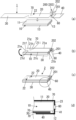
- FIG. 6C is an enlarged front view of a portion circled in FIG. 6B.
- 13A and 13B are equivalent circuit diagrams of an RF tag according to a second embodiment of the present invention
- 9(a) is a plan view showing the structure of an RF tag antenna according to a third embodiment
- FIG. 9(b) is an enlarged plan view of a portion circled in FIG. 9(a)
- 10(a) is a plan view showing the structure of an RF tag antenna according to a fourth embodiment
- FIG. 10(b) is an enlarged plan view of a portion circled in FIG.
- the RF tag antenna 1 includes an insulating substrate 10, a main waveguide element 20, a ground plate 30, a sub-waveguide element 40, a coating layer 70 made of an insulating material, and a frequency adjustment capacitor 203.
- the main waveguide element 20, the ground plate 30, and the sub-waveguide element 40 are formed on the surface of the coating layer 70.
- the RF tag 2 is configured by attaching an IC chip 60 to the RF tag antenna 1.
- the insulating substrate 10 has a surface 11, a back surface 12, and a side surface 13.
- the shape of the insulating substrate 10 is, for example, a substantially rectangular parallelepiped, but is not limited thereto and may be, for example, a disk-like or arc-shaped curved shape. It is preferable that the insulating substrate 10 has a shape that corresponds to the surface shape of the object to which the RF tag 2 is to be attached. For example, if the object is cylindrical and the RF tag 2 is to be attached to its curved surface, it is preferable that the shape of the RF tag 2 matches the curvature of the curved surface.
- the insulating substrate 10 may be made of polystyrene foam, polyethylene, polyimide, or the like. Furthermore, the insulating substrate 10 may be made of a dielectric material such as ceramic, paper, or resin.
- the main waveguide element 20 is provided on the surface 11 of the insulating substrate 10.
- the main waveguide element 20 of this embodiment has a rectangular shape, and is formed by a known method such as etching a thin metal film such as aluminum or pattern printing.
- the ground plane 30 is electrically connected to the main waveguide element 20 and is provided on the back surface 12 of the insulating substrate 10.
- the ground plane 30 in this embodiment has a rectangular shape, and is formed on the surface of the coating layer 70 by a known method such as etching a thin metal film of aluminum or the like, or pattern printing, in the same manner as the main waveguide element 20.
- the secondary waveguide element 40 is not directly (physically) connected to the primary waveguide element 20, that is, the edges are cut off.
- a protruding portion 41 is provided on a part of the side of the secondary waveguide element 40, and a protruding portion 23 is provided on a part of the side of the primary waveguide element 20.
- One terminal of the IC chip 60 is connected to the protruding portion 41, and the other terminal is connected to the protruding portion 23 of the primary waveguide element 20, so that the secondary waveguide element 40 and the primary waveguide element 20 are connected via the IC chip 60.
- both terminals of the IC chip 60 may be directly connected to the secondary waveguide element 40 and the primary waveguide element 20 without providing the protruding portions 23 and 41.
- the coating layer 70 is folded at the side of the insulating substrate 10 (see the arrow) and attached to the insulating substrate 10 via an adhesive layer (not shown).
- the auxiliary waveguide element 40 overlaps with the ground plate 30 via the coating layer 70, and the auxiliary waveguide element 40, the coating layer 70, and the ground plate 30 form a capacitor 80 (see FIG. 2).
- the main waveguide element 20, the base plate 30, and the secondary waveguide element 40 are formed on the surface of the coating layer 70, but the coating layer 70 need only be present at least in the portion where the secondary waveguide element 40 and the base plate 30 overlap.
- the resonant frequency can be adjusted by changing the area of the portion where the secondary waveguide element 40 overlaps with the base plate 30 via the coating layer 70.
- the material of the coating layer 70 is not particularly limited as long as it has flexibility and insulating properties, and may be, for example, PET, polyimide, vinyl, etc.
- the thickness of the coating layer 70 is not particularly limited, but is generally about several tens of ⁇ m.
- the main waveguide element 20, the ground plane 30 and the secondary waveguide element 40 surround the insulating substrate 10 in an annular shape.
- the main wave element 20 is preferably designed so that the total length L of its sides 21a to 21i is either ⁇ /4, ⁇ /2, 3 ⁇ /4, or 5 ⁇ /8. ⁇ is the wavelength of the radio waves transmitted from the reading device. In this embodiment, the length of the side is adjusted to be large by providing a notch 22 on the side of the main wave element 20.
- the main wave element 20 may be configured without the notch 22.
- the frequency adjustment capacitor 203 is provided between the primary waveguide element 20 and the secondary waveguide element 40 .
- the frequency adjusting capacitor 203 of this embodiment is composed of a frequency adjusting element 200 having an insulating layer 201 and a conductive layer 202 .
- the insulating layer 201 is made of an insulator and is placed between the main waveguide element 20 and the sub-guiding element 40.
- a conductive layer 202 is placed on the insulating layer 201.
- the conductive layer 202 needs to be long enough to overlap with the main waveguide element 20 and the sub-guiding element 40.
- the upper part of the insulating layer 201 is covered with the conductive layer 202, and a part of the lower part of the insulating layer 201 is covered with the main waveguide element 20 and the sub-guiding element 40, forming a frequency adjustment capacitor 203.
- the IC chip 60 operates based on the radio waves received by the RF tag antenna 1. Specifically, the IC chip 60 rectifies part of the carrier waves transmitted from the reader and generates the power supply voltage required for operation. The IC chip 60 then uses the generated power supply voltage to operate the control logic circuit within the IC chip 60 and the non-volatile memory that stores the product's unique information, and to operate communication circuits for sending and receiving data to and from the reader.
- a resonant circuit is configured to resonate in the frequency band of the received radio waves.
- This resonant circuit is configured with an inductor pattern, a capacitor 80, and an IC chip 60, as shown in the equivalent circuit diagram of Figure 3.
- the inductor pattern is configured with a primary waveguide element 20 and a ground plane 30.
- the primary waveguide element 20 and the secondary waveguide element 40 are connected by the equivalent capacitance of the IC chip 60.
- the capacitor 80 is composed of the sub-waveguide element 40, the coating layer 70 and the ground plane 30 as described above.
- Some IC chips 60 include a capacitor therein, and the IC chips 60 have stray capacitance. For this reason, when setting the resonant frequency of the resonant circuit, it is preferable to take into consideration the equivalent capacitance inside the IC chip 60. In other words, it is preferable for the resonant circuit to have a resonant frequency that is set in consideration of the inductance of the inductor pattern L, the capacitance of the capacitor 80, and the equivalent capacitance inside the IC chip 60.
- the resonant frequency f 0 [Hz] of this series resonant circuit is given by the following formula (1):
- the value of the resonant frequency f 0 is preferably set to be approximately the center value of the frequency bandwidth of the multiple radio waves transmitted from the reader.
- La is the inductance of the inductor pattern
- Ca is the capacitance of the capacitor 80
- Cb is the equivalent capacitance inside the IC chip 60. Note that, for example, a capacitance value published as one of the specifications of the IC chip 60 to be used can be used as Cb.
- the resonant frequency f0 of the resonant circuit can be set accurately to the frequency band of the radio wave.
- the reading performance of the RF tag 2 can be improved.
- the power supply voltage generated by the IC chip 60 can be increased.
- 3(b) shows a case where the area of the portion where the auxiliary waveguide element 40 overlaps with the ground plane 30 via the coating layer 70 is relatively large (see the circled area in FIG. 3(b)). In this way, by changing the area of the portion where the auxiliary waveguide element 40 overlaps with the ground plane 30 via the coating layer 70, it is possible to adjust Ca and thereby adjust the resonant frequency f0 .
- the inductance La can be increased by annularly surrounding the insulating substrate 10 with the primary waveguide element 20, the ground plate 30, and the secondary waveguide element 40.
- the resistance value increases, and the Q value of the series resonant circuit decreases based on the resistance value, resulting in a wider bandwidth and an RF tag antenna and an RF tag that can operate over a wide frequency band.
- the impedance becomes higher and the resonant frequency becomes lower. As a result, it becomes difficult to tune to the target resonant frequency f 0.
- the RF tag antenna 1 of the present invention is characterized in that it includes a frequency adjustment capacitor 203 (frequency adjustment element 200).
- a frequency adjustment capacitor 203 frequency adjustment element 200
- the main waveguide element 20 and the ground plane 30 constituting the inductor pattern L are also reduced in size.
- the frequency f0 in the above formula (1) becomes high, and there is a risk of it being outside the desired frequency band. Therefore, by providing a frequency adjustment capacitor 203 in a position parallel to the IC chip 60, the resonance frequency f 0 [Hz] is given by equation (2), and f 0 can be adjusted to a low value.
- La is the inductance of the inductor pattern L
- Ca is the capacitance of the capacitor 80
- Cb is the equivalent capacitance inside the IC chip 60
- Cc is the capacitance of the frequency adjustment capacitor 203.
- both ends of the short circuit are electrically connected to the first and second waveguide elements to form a planar inverted-F antenna (see FIG. 4C of Patent No. 6705116).
- an insulator layer 201 is placed across the primary waveguide element 20 and the secondary waveguide element 40, and a conductor layer 202 is placed on top of that.
- the conductor layer 202 is not electrically connected to the primary waveguide element 20 and the secondary waveguide element 40, and that the RF tag antenna 5 does not form a planar inverted-F antenna.
- Figure 4 is a graph showing the radio wave frequency (horizontal axis) and reading distance (vertical axis) of the RF tag antenna 1.
- the radio wave frequency horizontal axis
- reading distance vertical axis
- one RF tag 2 can be used for two frequency bands: the low frequency side (around 860 MHz) used mainly in Europe, and the high frequency side (around 920 MHz) used mainly in Japan.
- the RF tag 2 attached to the conductor 100 will be described with reference to FIGS.
- the RF tag 2 of the present invention can be used as it is, or can be used by contacting it with a conductor 100 .
- the back side of the RF tag 2 can be attached to the conductor 100 using an adhesive layer 101 made of an insulating material.
- the term "conductor” is a general term for a material with a relatively high electrical conductivity, similar to the general dictionary meaning, with metal being a typical example.
- the "conductor” is not limited to metal, and may be, for example, the human body, grass, trees, water, the ground, etc.
- a capacitor 81 with a coupling capacitance C is formed consisting of the ground plate 30, the sub-wave director element 40, the adhesive layer 101, and the conductor 100, so that the conductor 100 can be used as a director due to the capacitive coupling effect.
- the RF tag 2 can receive not only radio waves that reach the front side of the conductor 100, but also radio waves that reach the back side of the conductor 100.
- the "Conductor front” line in FIG. 4 shows the case where radio waves that reach the front side of the conductor 100 are read, and the "Conductor back” line shows the case where radio waves that reach the back side of the conductor 100 are read.
- the RF tag antenna 3 of this embodiment connects the secondary waveguide element 40 and the ground plate 30 via an IC chip 60. It is characterized in that at least a part of the secondary waveguide element 40 overlaps with the primary waveguide element 20 via a coating layer 70, so that a capacitor 82 is formed by the secondary waveguide element 40, the coating layer 70 and the primary waveguide element 20.
- the main waveguide element 20, the ground plane 30 and the secondary waveguide element 40 surround the insulating substrate 10 in an annular shape.
- the frequency adjustment capacitor 203 is provided between the ground plane 30 and the secondary director element 40. The resonant frequency can be adjusted by changing the area of the portion where the secondary director element 40 overlaps with the primary director element 20 via the coating layer 70.
- a resonant circuit is configured to resonate in the frequency band of the received radio waves.
- This resonant circuit is configured with an inductor pattern, a capacitor 82, a frequency adjustment capacitor 203, and an IC chip 60, as shown in the equivalent circuit diagram of Fig. 8.
- the inductor pattern is configured with a primary waveguide element 20 and a ground plate 30.
- the secondary waveguide element 40 and the ground plate 30 are connected through the equivalent capacitance of the IC chip 60.
- the capacitor 82 is comprised of the secondary waveguide element 40, the cladding layer 70 and the primary waveguide element 20 as described above.
- the inductance La is increased by annularly surrounding the insulating substrate 10 with the primary waveguide element 20, the ground plate 30, and the secondary waveguide element 40.
- the resistance value increases, and the Q value of the series resonant circuit decreases based on the resistance value, resulting in a wider bandwidth and an RF tag antenna 3 and an RF tag 4 that operate over a wide frequency band.
- 8(b) shows a case where the area of the portion where the secondary waveguide element 40 overlaps with the primary waveguide element 20 via the coating layer 70 is relatively large (see the circled area in FIG. 8(b)). In this way, by changing the area of the portion where the secondary waveguide element 40 overlaps with the primary waveguide element 20 via the coating layer 70, it is possible to adjust Ca in the above formula (2) and thereby adjust the resonant frequency f0 .
- FIG. 9 A third embodiment of an antenna for an RF tag and an RF tag according to the present invention will be described with reference to the drawings.
- the same reference numerals will be used to designate parts having the same configuration as those of the above-described embodiments, and the description thereof will be omitted.
- this embodiment is characterized in that the frequency adjustment capacitor 203 is composed of a first extension piece 204 extending from the end of the main waveguide element 20 toward the secondary waveguide element 40, a second extension piece 205 extending from the end of the secondary waveguide element 40 toward the main waveguide element 20 opposite the first extension piece 204, and a gap 206 formed between the tip of the first extension piece and the tip of the second extension piece.
- the first extension piece 204 is T-shaped and is composed of a base portion 204a extending from the end portion of the main waveguide element 20 toward the secondary waveguide element 40, and a tip portion 204b extending from the tip of the base portion 204a in a direction perpendicular to the base portion 204a.
- the second extension piece 205 is also T-shaped and is composed of a base portion 205a extending from the end portion of the secondary waveguide element 40 toward the primary waveguide element 20, and a tip portion 205b extending from the tip of the base portion 205a in a direction perpendicular to the base portion 205a.
- the two tip portions 204b, 205b are arranged in parallel with a gap 206 therebetween.
- the first extension piece and the second extension piece are formed by a known method such as etching a thin metal film such as aluminum or pattern printing.
- a capacitor is formed by the two tip portions 204b, 205b and the gap 206.
- the resonance frequency f 0 [Hz] is given by the above formula (2), and f 0 can be adjusted to a low value.
- the capacitance C C of the frequency adjustment capacitor 203 can be changed, and f 0 can be adjusted.
- the frequency adjustment capacitor is composed of an island piece 207 arranged in an island shape between the main waveguide element 20 and the secondary waveguide element 40, and gaps 208a to 208d formed between the island piece 207 and the main waveguide element 20 and between the island piece 207 and the secondary waveguide element 40.
- the island-like pieces 207 are formed by a known method such as etching a thin metal film such as aluminum or pattern printing.
- two island pieces 207 are arranged on either side of the IC chip 60 to form four gaps 208a to 208d, which results in four capacitors 209a to 209d being configured as frequency adjustment capacitors as shown in FIG. 11.
- the capacitance Cd of the frequency adjustment capacitor is given by equation (3).
- the resonance frequency f0 [Hz] is given by equation (4), and f0 can be adjusted to a low value.
- the capacitance Cd of the frequency adjustment capacitor can be changed to adjust f0 .
- Cd is the capacitance of the frequency adjustment capacitor
- C1 is the capacitance of capacitor 209a
- C2 is the capacitance of capacitor 209b
- C3 is the capacitance of capacitor 209c
- C4 is the capacitance of capacitor 209d.
- La is the inductance of the inductor pattern L
- Ca is the capacitance of the capacitor 80
- Cb is the equivalent capacitance inside the IC chip 60
- Cd is the capacitance of the frequency adjustment capacitor.
- FIG. 12(a) A fourth embodiment of the RF tag antenna and RF tag of the present invention will be described with reference to the drawings.
- the same reference numerals will be used to designate the same components as those of the above-described embodiments, and the description thereof will be omitted.
- an L-shaped slit 42 is provided in a part of the secondary waveguide element 40 to form a tongue-shaped piece 210, and the base of the tongue-shaped piece 210 is bent at the dotted line and joined to the back surface of the primary waveguide element 20 via an insulator to insulate the primary waveguide element 20 from the tongue-shaped piece 210 as shown in FIG. 12(b), to form a frequency adjustment capacitor.
- the frequency adjustment capacitor is composed of a primary waveguide element 20, a secondary waveguide element 40, a coating layer 70 made of an insulating material, and a tongue-shaped piece 210.
- a tongue-shaped piece may be formed by providing a slit in part of the main waveguide element 20, and the base of the tongue-shaped piece may be folded and joined to the back surface of the secondary waveguide element 40 via an insulator to insulate the secondary waveguide element 40 from the tongue-shaped piece, thereby forming a frequency adjustment capacitor.
- a tongue-shaped piece 210 may be formed by providing an L-shaped slit 42 in a part of the secondary waveguide element 40, and the base of the tongue-shaped piece 210 may be folded at the dotted line and joined to the rear surface of the base plate 30 via an insulator to insulate the base plate 30 from the tongue-shaped piece 210 as shown in FIG. 13(b), thereby forming a frequency adjustment capacitor.
- the frequency adjustment capacitor is composed of a ground plane 30, a sub-wave director element 40, a coating layer 70 made of an insulating material, and a tongue-shaped piece 210.
- a tongue-shaped piece may be formed by providing a slit in part of the base plate 30, and the base of the tongue-shaped piece may be bent and joined to the rear surface of the secondary waveguide element 40 to form a frequency adjustment capacitor.
- FIG. 14 shows a comprehensive list of modified examples of the RF tag antenna and RF tag of the present invention.
- FIG. 14( a ) shows a configuration in which the secondary director element 40 , the primary director element 20 , and the ground plane 30 are wrapped around the insulating substrate 10 with the coating layer 70 in contact with the insulating substrate 10 , and the surface of the secondary director element 40 is covered with part of the ground plane 30 .
- FIG. 14(b) shows a configuration in which the secondary waveguide element 40, the ground plane 30, and the main waveguide element 20 are wrapped around the insulating substrate 10 with the coating layer 70 in contact with the insulating substrate 10, and the surface of the secondary waveguide element 40 is covered with part of the main waveguide element 20.
- FIG. 14(c) shows a configuration in which the coating layer 70 is exposed to the outside, that is, turned upside down from the state shown in FIG. 1(a), the main waveguide element 20 and the ground plate 30 are wrapped around the insulating substrate 10, and part of the surface of the ground plate 30 is covered with the sub-guiding element 40.
- the IC chip 60 is not exposed to the outside, so the risk of damage can be reduced.
- FIG. 14( d ) shows a configuration in which the main waveguide element 20 and the ground plane 30 are wrapped around the insulating substrate 10 with the coating layer 70 exposed to the outside, and part of the surface of the main waveguide element 20 is covered with the secondary waveguide element 40 .
- FIG. 14( e ) shows a configuration in which the secondary waveguide element 40, the primary waveguide element 20 and the ground plate 30 are wrapped around an insulating substrate 10 with the coating layer 70 exposed to the outside, and the surface of the secondary waveguide element 40 is covered with part of the ground plate 30 .
- FIG. 14( f ) shows a configuration in which the secondary waveguide element 40, the ground plane 30, and the main waveguide element 20 are wrapped around the insulating substrate 10 with the coating layer 70 exposed to the outside, and the surface of the secondary waveguide element 40 is covered with part of the main waveguide element 20 .
- an RF tag antenna and an RF tag that operate in a wide frequency band can be obtained.
- a frequency adjustment capacitor is provided in any of the configurations shown in Figures 14(a) to (f).
- the present invention is an antenna for RF tags and an RF tag that operate over a wide frequency band, and has industrial applicability.
- RF tag antenna 1.
- RF tag antenna 2.
- RF tag 3. RF tag antenna 4.
- RF Tag 10 Insulating substrate 11 Surface 12 Back 13 Side 20 Main Wave Element 21a to 21i Side 22 Cut 23 Convex 30 Main plate 40
- Sub-waveguide element 41
- Convex 42 Slit 60
- IC chips 70
- Coating Layer 80
- Capacitor 81 Capacitor 82
- Conductor 101 Adhesive layer
- Frequency Adjustment Element 201
- Conductive layer 203
- Frequency adjustment capacitor 204 First extension piece 204a Base 204b Tip 205 2nd extension piece 205a
- Base 205b Tip 206 Gap 207 Island 208a to 208d Gap 209a to 209d
Landscapes
- Engineering & Computer Science (AREA)
- Computer Hardware Design (AREA)
- Microelectronics & Electronic Packaging (AREA)
- Physics & Mathematics (AREA)
- General Physics & Mathematics (AREA)
- Theoretical Computer Science (AREA)
- Waveguide Aerials (AREA)
Abstract
L'invention concerne une antenne pour étiquettes RF qui fonctionne dans une large bande de fréquences, et une étiquette RF. Une antenne (1) pour étiquettes RF selon la présente invention comprend un substrat isolant (10), un élément de guide d'ondes principal (20), une plaque de base (30) qui est électriquement connectée à l'élément de guide d'ondes principal, un élément de guide d'ondes auxiliaire (40) qui est connecté à l'élément de guide d'ondes principal par l'intermédiaire d'une puce IC (60), et un condensateur (203) pour un réglage de fréquence. Au moins une partie de l'élément de guide d'ondes auxiliaire chevauche la plaque de base avec une couche de revêtement (70) composée d'un matériau isolant interposé entre celles-ci, moyennant quoi un condensateur est formé par l'élément de guide d'ondes auxiliaire, la couche de revêtement et la plaque de base. Le substrat isolant est enfermé sous forme d'anneau par l'élément de guide d'ondes principal, la plaque de base et l'élément de guide d'ondes auxiliaire. Le condensateur pour le réglage de fréquence est disposé entre l'élément de guide d'ondes principal et l'élément de guide d'ondes auxiliaire. En raison du fait que le substrat isolant est enfermé sous forme d'anneau, l'inductance augmente, une valeur de résistance augmente, et la valeur Q d'un circuit de résonance en série diminue. Par conséquent, une largeur de bande augmente, ce qui permet d'obtenir une antenne pour des étiquettes RF qui fonctionne dans une large bande de fréquences et une étiquette RF.
Applications Claiming Priority (2)
| Application Number | Priority Date | Filing Date | Title |
|---|---|---|---|
| JP2022159493 | 2022-10-03 | ||
| JP2022-159493 | 2022-10-03 |
Publications (1)
| Publication Number | Publication Date |
|---|---|
| WO2024075325A1 true WO2024075325A1 (fr) | 2024-04-11 |
Family
ID=90608202
Family Applications (1)
| Application Number | Title | Priority Date | Filing Date |
|---|---|---|---|
| PCT/JP2023/014141 WO2024075325A1 (fr) | 2022-10-03 | 2023-04-05 | Antenne pour étiquettes rf et étiquette rf |
Country Status (1)
| Country | Link |
|---|---|
| WO (1) | WO2024075325A1 (fr) |
Citations (6)
| Publication number | Priority date | Publication date | Assignee | Title |
|---|---|---|---|---|
| JPS62123342A (ja) * | 1985-08-23 | 1987-06-04 | Jeol Ltd | 電子スピン共鳴装置のル−プギヤツプ共振器 |
| JP2011109552A (ja) * | 2009-11-20 | 2011-06-02 | Fujitsu Ltd | 無線タグ |
| WO2011155402A1 (fr) * | 2010-06-09 | 2011-12-15 | 株式会社村田製作所 | Procédé de fabrication d'antenne, antenne, et procédé de fabrication de dispositif à circuit intégré sans fil |
| US20140284388A1 (en) * | 2011-11-25 | 2014-09-25 | Zhijia Liu | Production Process of Tag Antenna |
| WO2015015604A1 (fr) * | 2013-07-31 | 2015-02-05 | 富士通株式会社 | Etiquette rfid et système rfid |
| US20220069435A1 (en) * | 2020-08-28 | 2022-03-03 | Securitag Assembly Group Co., Ltd. | Antenna structure and device for metal environment |
-
2023
- 2023-04-05 WO PCT/JP2023/014141 patent/WO2024075325A1/fr unknown
Patent Citations (6)
| Publication number | Priority date | Publication date | Assignee | Title |
|---|---|---|---|---|
| JPS62123342A (ja) * | 1985-08-23 | 1987-06-04 | Jeol Ltd | 電子スピン共鳴装置のル−プギヤツプ共振器 |
| JP2011109552A (ja) * | 2009-11-20 | 2011-06-02 | Fujitsu Ltd | 無線タグ |
| WO2011155402A1 (fr) * | 2010-06-09 | 2011-12-15 | 株式会社村田製作所 | Procédé de fabrication d'antenne, antenne, et procédé de fabrication de dispositif à circuit intégré sans fil |
| US20140284388A1 (en) * | 2011-11-25 | 2014-09-25 | Zhijia Liu | Production Process of Tag Antenna |
| WO2015015604A1 (fr) * | 2013-07-31 | 2015-02-05 | 富士通株式会社 | Etiquette rfid et système rfid |
| US20220069435A1 (en) * | 2020-08-28 | 2022-03-03 | Securitag Assembly Group Co., Ltd. | Antenna structure and device for metal environment |
Similar Documents
| Publication | Publication Date | Title |
|---|---|---|
| JP4186149B2 (ja) | Icカード用の補助アンテナ | |
| KR100781933B1 (ko) | 단일 급전 단층 2 중 대역 원편파 안테나 | |
| JP4393228B2 (ja) | 小型アンテナ及びそれを備えた無線タグ | |
| US7504998B2 (en) | PIFA and RFID tag using the same | |
| JP4333821B2 (ja) | 無線icデバイス | |
| KR100970072B1 (ko) | 태그 안테나, 및 태그 | |
| US8174454B2 (en) | Dual-band antenna | |
| US8678295B2 (en) | Miniaturized radio-frequency identification tag and microstrip patch antenna thereof | |
| EP1653396B1 (fr) | Etiquette RFID | |
| US8196829B2 (en) | Chip module, sim card, wireless device and wireless communication method | |
| JP5265411B2 (ja) | アンテナ装置及び電子機器 | |
| CN109219906B (zh) | 天线装置 | |
| US20080122628A1 (en) | RFID tag antenna and RFID tag | |
| KR20100021665A (ko) | 안테나 및 비접촉형 태그 | |
| KR100756410B1 (ko) | Rfid 트랜스폰더에 사용되는 소형 렉테나 | |
| US7375697B2 (en) | Meandered slit antenna | |
| WO2024075325A1 (fr) | Antenne pour étiquettes rf et étiquette rf | |
| CN114861850B (zh) | 一种电子标签 | |
| KR100767720B1 (ko) | 이중대역 도체스트립 개방루프 안테나 및 이를 이용한휴대용 전자태그 리더 | |
| WO2022118595A1 (fr) | Antenne à étiquette double radiofréquence (rf) et étiquette double rf | |
| KR100968711B1 (ko) | Rfid태그 안테나 | |
| JP2024033152A (ja) | 導波機能付きrfid用カバー及びrfidタグセット | |
| JP5328803B2 (ja) | 無線通信装置 | |
| WO2019225526A1 (fr) | Antenne d'étiquette rf, étiquette rf et étiquette rf avec conducteur | |
| JP2007336156A (ja) | ループアンテナ |
Legal Events
| Date | Code | Title | Description |
|---|---|---|---|
| 121 | Ep: the epo has been informed by wipo that ep was designated in this application |
Ref document number: 23874461 Country of ref document: EP Kind code of ref document: A1 |