WO2024075267A1 - ノイズフィルタ、電力変換システム及び管理システム - Google Patents
ノイズフィルタ、電力変換システム及び管理システム Download PDFInfo
- Publication number
- WO2024075267A1 WO2024075267A1 PCT/JP2022/037561 JP2022037561W WO2024075267A1 WO 2024075267 A1 WO2024075267 A1 WO 2024075267A1 JP 2022037561 W JP2022037561 W JP 2022037561W WO 2024075267 A1 WO2024075267 A1 WO 2024075267A1
- Authority
- WO
- WIPO (PCT)
- Prior art keywords
- cancellation signal
- noise filter
- power conversion
- unit
- noise
- Prior art date
- Legal status (The legal status is an assumption and is not a legal conclusion. Google has not performed a legal analysis and makes no representation as to the accuracy of the status listed.)
- Ceased
Links
Images














Classifications
-
- H—ELECTRICITY
- H02—GENERATION; CONVERSION OR DISTRIBUTION OF ELECTRIC POWER
- H02M—APPARATUS FOR CONVERSION BETWEEN AC AND AC, BETWEEN AC AND DC, OR BETWEEN DC AND DC, AND FOR USE WITH MAINS OR SIMILAR POWER SUPPLY SYSTEMS; CONVERSION OF DC OR AC INPUT POWER INTO SURGE OUTPUT POWER; CONTROL OR REGULATION THEREOF
- H02M1/00—Details of apparatus for conversion
Definitions
- This disclosure relates to noise filters, power conversion systems, and management systems.
- Power conversion devices are known that convert input power from a power source into any DC or AC power and supply it to a load. Such power conversion devices perform power conversion by opening and closing multiple bridge-connected switching elements, but high-frequency noise is generated as the switching elements operate. This high-frequency noise passes through parasitic capacitance and other factors to the ground potential, causing common-mode noise to flow to the power source or load. Therefore, in order to suppress such common-mode noise, a configuration is known in which a noise filter is installed in the electrical path between the power source and the power conversion device, or in the electrical path between the power conversion device and the load.
- the active noise filter described in Patent Document 1 detects the common mode voltage via a grounded capacitor connected to the electrical path between the AC power supply and the rectifier, generates a cancellation voltage of the same magnitude and opposite polarity as the common mode voltage detected by a cancellation voltage source, and superimposes the cancellation voltage between the connection point of the AC power supply and the grounded capacitor in the electrical path.
- the active noise filter described in Patent Document 1 injects a cancellation voltage that cancels out the common mode voltage, which is common mode noise, into the electrical path as a noise cancellation signal (hereinafter referred to as a cancellation signal).
- control characteristics of the active noise filter may change due to environmental factors or factors that have passed over time.
- an abnormal cancellation signal such as the cancellation signal injected into the electrical circuit oscillating due to a loss of control margin (gain margin and phase margin) or the amount of compensation in noise cancellation becoming excessive.
- This disclosure has been made to solve the problems described above, and aims to provide a noise filter, power conversion system, and management system that can achieve high reliability.
- the noise filter disclosed in the present application comprises: A noise filter provided in either an electric path connecting an AC or DC power source and a power conversion device that converts power output from the AC or DC power source into AC or DC power, or an electric path connecting the power conversion device and a load, A noise detection unit that detects common mode noise generated during operation of the power conversion device; a cancellation signal generating unit that generates a cancellation signal that cancels the common mode noise; a cancellation signal injection unit that injects the cancellation signal into the electrical path; an abnormality detection unit that outputs an abnormality detection signal when detecting that the cancellation signal is abnormal; The abnormality processing sequence is executed based on the abnormality detection signal.
- the power conversion system disclosed in the present application comprises: a power conversion device that converts power output from an AC or DC power source into AC or DC power; The noise filter described above.
- the management system disclosed in the present application comprises: a power conversion device that converts power output from an AC or DC power source into AC or DC power;
- the noise filter further includes a communication unit connected to a cancellation signal output unit constituting the noise filter and configured to transmit data to an outside.
- a management device having a database for storing the data transmitted from the communication unit and a data analysis unit for analyzing the data.
- the noise filter and power conversion system disclosed in this application have the effect of providing high reliability by operating stably even when an abnormality occurs in the cancellation signal.
- the management system disclosed in this application has a management device that performs data analysis using data transmitted from the power conversion system, making it possible to quickly address the cause of an abnormality, which has the effect of further improving the reliability of the power conversion system and also has the effect of improving the maintainability of the power conversion system, such as management and maintenance.
- FIG. 1 is a system configuration diagram illustrating a power conversion system according to a first embodiment.
- 1 is a circuit configuration diagram illustrating a power conversion device constituting a part of a power conversion system according to a first embodiment.
- 4A to 4C are diagrams illustrating common mode noise generated in the power conversion system according to the first embodiment.
- 1 is a configuration diagram illustrating a noise filter and a power conversion system according to a first embodiment.
- 2 is a configuration diagram illustrating an example of a noise detection unit in the noise filter according to the first embodiment.
- FIG. 2 is a configuration diagram illustrating an example of a noise detection unit in the noise filter according to the first embodiment.
- FIG. 4 is a configuration diagram illustrating an example of a cancellation signal generating section in the noise filter according to the first embodiment.
- FIG. 2 is a configuration diagram illustrating an example of an abnormality detection unit in the noise filter according to the first embodiment.
- FIG. 2 is a configuration diagram illustrating an example of a feature detection unit in the noise filter according to the first embodiment.
- FIG. 4 is a configuration diagram illustrating an example of a feature comparison unit in the noise filter according to the first embodiment.
- FIG. 2 is a configuration diagram illustrating a cancellation signal injection section in the noise filter according to the first embodiment.
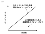
- FIG. 4 is a diagram illustrating the relationship between the impedance and frequency of an injection transformer during normal operation in the noise filter according to the first embodiment.
- FIG. 5A and 5B are diagrams for explaining behavior during a protective operation of an injection transformer in the noise filter according to the first embodiment.
- 5 is a diagram illustrating the relationship between impedance and frequency during a protective operation of an injection transformer in the noise filter according to the first embodiment.
- FIG. 2 is a configuration diagram illustrating an example of a protection circuit in the noise filter according to the first embodiment.
- FIG. FIG. 11 is a configuration diagram illustrating a noise filter according to a second embodiment.
- FIG. 11 is a configuration diagram illustrating another configuration example of the noise filter according to the second embodiment.
- FIG. 10A and 10B are diagrams illustrating an example of processing of an abnormality detection signal in a cancellation signal output unit in the noise filter according to the second embodiment.
- FIG. 11 is a configuration diagram illustrating a power conversion system according to a third embodiment.
- 13A and 13B are diagrams illustrating common mode noise generated in a power conversion system according to a third embodiment.
- FIG. 11 is a configuration diagram illustrating a noise filter according to a third embodiment.
- FIG. 21A is a diagram showing the control response when there is no filter portion
- FIG. 21B is a diagram showing the pass characteristics of the filter portion
- FIG. 21C is a diagram showing the control response when there is a filter portion.
- FIG. 21A is a diagram showing the control response when there is no filter portion
- FIG. 21B is a diagram showing the pass characteristics of the filter portion
- FIG. 21C is a diagram showing the control response when there is a filter portion.
- FIG. 21A is a diagram showing the control response when there is no filter
- FIG. 22A is a graph showing the gain characteristic
- FIG. 22B is a graph showing the phase characteristic.
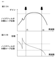
- FIG. 23A is a graph showing the change in gain characteristics when a change occurs in the control characteristics due to the occurrence of an abnormality
- FIG. 23B is a graph showing the change in phase characteristics when a change occurs in the control characteristics due to the occurrence of an abnormality.
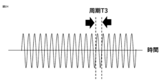
- 11 is a diagram illustrating an abnormal output waveform of a cancellation signal output section of a noise filter.
- 25A is a diagram showing the waveform of a common mode voltage under normal conditions
- FIG. 25B is a diagram showing the waveform of a common mode current under normal conditions
- FIG. 25A is a diagram showing the waveform of a common mode voltage under normal conditions
- FIG. 25B is a diagram showing the waveform of a common mode current under normal conditions
- FIG. 25C is a diagram showing the waveform of an output voltage of a cancellation signal in a noise filter under normal conditions
- FIG. 25D is a diagram showing the waveform of an output current of a cancellation signal in a noise filter under normal conditions.
- FIG. 26A is a diagram showing the waveform of a common mode voltage during an abnormality
- FIG. 26B is a diagram showing the waveform of a common mode current during an abnormality
- FIG. 26C is a diagram showing the waveform of an output voltage of a cancellation signal during an abnormality
- FIG. 26D is a diagram showing the waveform of an output current of a cancellation signal during an abnormality.
- FIG. 11 is a configuration diagram illustrating a noise filter and a power conversion system according to a fourth embodiment.
- FIG. 11 is a configuration diagram illustrating a noise filter and a power conversion system according to a fourth embodiment.
- FIG. 13 is a configuration diagram showing a management system according to a fifth embodiment.
- FIG. 13 is a configuration diagram illustrating a noise filter and a power conversion system according to a fifth embodiment.
- FIG. 13 is a configuration diagram illustrating a noise filter and a power conversion system according to a sixth embodiment.
- Embodiment 1 A noise filter 100 and a power conversion system 500 according to the first embodiment will be described with reference to Fig. 1 to Fig. 11.
- Fig. 1 is a system configuration diagram showing the power conversion system 500 according to the first embodiment
- Fig. 2 is a circuit configuration diagram showing a power conversion device 80 constituting a part of the power conversion system 500 according to the first embodiment.
- the power conversion system 500 is arranged between an AC power source 1 and a load 90, and is composed of a power conversion device 80 that converts input power from the AC power source 1 into any DC power or AC power, the load 90 to which any DC power or AC power is supplied from the power conversion device 80, and a noise filter 100 provided on an electric circuit 11 that connects the power conversion device 80 and the load 90.
- the input power from the AC power source 1 is input to the power conversion device 80 via an electric circuit 2.
- the AC power source 1 is merely one example of a power source, and a DC power source may be used instead of the AC power source 1, and similarly, a DC power source may be used instead of the AC power source 1 in each of the embodiments described below.
- the power conversion device 80 converts the input power input from the AC power source 1 into the power required to drive the load 90 and outputs it.
- the noise filter 100 is disposed between the power conversion device 80 and the load 90, but it may also be provided in the electrical path 2 that connects the AC power source 1 and the power conversion device 80.
- the power conversion device 80 is, for example, a two-level three-phase inverter as shown in FIG. 2. That is, one upper and lower arm 82 is formed by two semiconductor switches 82a, 82b connected in series. Furthermore, one upper and lower arm 83 is formed by two semiconductor switches 83a, 83b connected in series. Furthermore, one upper and lower arm 84 is formed by two semiconductor switches 84a, 84b connected in series. A DC power supply 81 is connected to these three upper and lower arms 82, 83, 84.
- the DC power supply 81 is composed of a converter that converts the AC input power input from the AC power supply 1 into DC.
- the midpoints of the three upper and lower arms 82, 83, and 84 are connected to the inverter output terminal 85.
- These six semiconductor switches 82a, 82b, 83a, 83b, 84a, and 84b perform switching operations, outputting AC power to the inverter output terminal 85.
- the output potential of the inverter output terminal 85 becomes either the positive voltage or the negative voltage of the DC power supply 81. Therefore, the common mode voltage of the power conversion device 80 becomes a constant voltage that is not zero.
- FIG. 3 is a diagram explaining the common mode noise generated in the power conversion system 500 according to the first embodiment, and shows a common mode equivalent circuit.
- the AC power source 1 and the load 90 are connected on the ground side by a ground wire 3, separate from the above-mentioned electric circuit 11.
- the noise filter 100 is provided with a ground capacitor 15 (not shown) having one end connected to the ground line 3.
- Parasitic capacitance 86 and parasitic capacitance 91 exist between the power conversion device 80 and the ground line 3, and between the load 90 and the ground line 3, respectively.
- a common mode voltage Vcn generated in the power conversion device 80 is applied to the common mode loop via the parasitic capacitances 86, 91 and the ground line 3, so that a common mode current (common mode noise CN) flows in the direction shown by the arrow in FIG. 3.
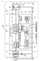
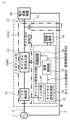
- FIG. 4 is a configuration diagram showing a noise filter 100 and a power conversion system 500 according to the first embodiment.
- the noise filter 100 is inserted between the power conversion device 80 and the load 90.
- the noise filter 100 is provided in an electrical path 11 that connects the power conversion device 80 and the load 90.
- the noise filter 100 comprises a noise detection unit 12 connected to the electrical circuit 2, a cancellation signal output unit 13 which generates and outputs a cancellation signal CS from common mode noise CN (not shown in FIG. 4) detected by the noise detection unit 12, a cancellation signal injection unit 14 which is provided on the electrical circuit 11 closer to the output end than the noise detection unit 12, i.e., on the load 90 side, and which injects the cancellation signal CS output from the cancellation signal output unit 13 into the electrical circuit 11, and a control power supply 19 which supplies power to the cancellation signal output unit 13 for generating and injecting the cancellation signal CS.
- the cancellation signal output unit 13 includes a cancellation signal generation unit 16 that amplifies the noise detection signal DS output from the noise detection unit 12, and an abnormality detection unit 17 that transmits the output from the cancellation signal generation unit 16 to the cancellation signal injection unit 14 as a cancellation signal CS and can output an abnormality detection signal AS based on the output voltage of the cancellation signal generation unit 16.
- the cancellation signal output unit 13 further includes a protection circuit 18, which is an example of a connection cut-off means that is inserted between the abnormality detection unit 17 and the cancellation signal injection unit 14 and can cut off the injection of the cancellation signal.
- the noise filter 100 according to the first embodiment includes a connection cut-off means that cuts off the connection between the cancellation signal output unit 13 and the cancellation signal injection unit 14, as a protection means for preventing the injection of an abnormal cancellation signal CS into the electrical circuit 11.
- the protection circuit 18 is used as one form of connection cut-off means.
- the abnormality detection unit 17 is composed of elements and circuits that have almost no effect on the output characteristics, so the output of the cancellation signal generation unit 16 is almost the same as the cancellation signal CS. Therefore, in the following explanation, unless otherwise specified, the output of the cancellation signal generation unit 16 will be referred to as the cancellation signal CS.
- a filter section capable of adjusting the characteristics of the cancellation signal CS may be provided between the noise detection section 12 and the cancellation signal generation section 16, or between the cancellation signal generation section 16 and the abnormality detection section 17.
- the cancellation signal generation section 16 will amplify the noise detection signal DS adjusted by the filter section to generate the cancellation signal CS. Even in this case, the characteristics of the cancellation signal CS will be adjusted by adjusting the noise detection signal DS.
- the above-mentioned filter section may be an input filter circuit that adjusts the attenuation characteristics of the noise filter 100, such as by reducing the gain of a specific band.
- an analog filter such as a high-pass filter, low-pass filter, or notch filter made up of resistors and capacitors may be used.
- a grounded capacitor 15 (not shown) is provided between the electric circuit 11 and the grounded wire 3.
- the noise detection unit 12, the cancellation signal injection unit 14, and the grounded capacitor 15 constitute the main circuit unit 101 of the noise filter 100.
- the control characteristics of the noise filter 100 are largely dependent on the main circuit unit 101.
- the inductance value of the main circuit unit 101 is the sum of the inductance value of the common mode transformer constituting the noise detection unit 12 and the inductance value of the common mode transformer constituting the cancellation signal injection unit 14.
- the capacitance value of the main circuit unit 101 is the capacitance value of the grounded capacitor 15.
- the power conversion system 500 includes a load 90, but the present invention is not limited to such a configuration.
- the main circuit unit 101 is constituted using a parasitic capacitance 91 that functions as the common mode impedance of the load 90.
- the control characteristics of the main circuit section 101 will be described in detail later.
- FIGS. 5A and 5B are configuration diagrams showing an example of the noise detection unit 12 in the noise filter 100 according to the first embodiment.
- the noise detection unit 12 is composed of a capacitor network.
- the multiple capacitors that make up the noise detection unit 12 are hereinafter referred to as the detection capacitor network 12n.
- the detection capacitor network 12n includes a detection capacitor 12a connected to the U-phase power line, a detection capacitor 12b connected to the V-phase power line, a detection capacitor 12c connected to the W-phase power line, and a detection capacitor 12e provided between the star connection point 12f connected to the other terminal of the detection capacitors 12a, 12b, and 12c that is not the power line and the ground wire 3 in the electric circuit 11 connecting the power conversion device 80 and the load 90.
- the detection capacitor network 12n operates as a noise detector that divides and detects the common mode voltage.
- the detection ratio of the common mode voltage in the detection capacitor network 12n is determined by the ratio between the parallel impedance of the detection capacitors 12a, 12b, and 12c and the impedance of the detection capacitor 12e. Therefore, in the noise detection unit 12, a noise detection signal DS is generated at both ends of the T-phase winding 12d due to the common mode noise CN applied to the detection capacitor network 12n.
- Both ends of the T-phase winding 12d are connected to the cancellation signal generating unit 16.
- the noise detection signal DS generated at both ends of the T-phase winding 12d is sent to the cancellation signal generating unit 16.
- the detection capacitor network 12n has an impedance that is sufficiently higher than the parasitic capacitance 86 of the inverter and the parasitic capacitance 91 of the load 90 in the common mode equivalent circuit shown in Figure 3, and therefore has a relatively high impedance to ground and does not adversely affect the leakage current of the power conversion device 80.
- FIG. 6 is a configuration diagram showing an example of the cancellation signal generating unit 16 in the noise filter 100 according to the first embodiment.
- the cancellation signal generating unit 16 includes an input resistor 16a, an operational amplifier 16b, and a feedback resistor 16c.
- the inverting input terminal of the operational amplifier 16b is connected to the input terminal side of the cancellation signal generating unit 16 (the left side in FIG. 6) via the input resistor 16a.
- the inverting input terminal of the operational amplifier 16b is connected to the output terminal of the operational amplifier 16b via the feedback resistor 16c.
- the non-inverting input terminal of the operational amplifier 16b is grounded.
- the cancellation signal generating unit 16 shown in FIG. 6 is an inverting amplifier circuit using the operational amplifier 16b, but it may also be a non-inverting amplifier circuit.
- the cancellation signal generating unit 16 amplifies the noise detection signal DS with an amplification factor given by the ratio between the resistance value of the input resistor 16a and the resistance value of the feedback resistor 16c to generate the cancellation signal CS, and outputs the cancellation signal CS.
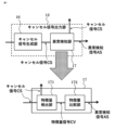
- FIG. 7 is a configuration diagram showing an example of the anomaly detection unit 17 in the noise filter 100 according to the first embodiment.
- the anomaly detection unit 17 is composed of a feature detection unit 171 that outputs a feature signal CV for detecting an anomaly using the output voltage of the cancellation signal CS, and a feature comparison unit 172 that generates and outputs an anomaly detection signal AS by performing a predetermined calculation on the feature signal CV.
- the anomaly detection signal AS is output as an on-output
- the anomaly detection signal AS is output as an off-output.
- FIG. 8 is a configuration diagram showing an example of a feature detection unit 171 that is part of the anomaly detection unit 17 in the noise filter 100 according to the first embodiment.
- the feature detection unit 171 generates and outputs a feature signal CV based on the voltage value of the output voltage as the cancellation signal CS.
- the feature signal CV is a signal that represents a feature used for anomaly detection. Various values can be assumed to be used as the feature.
- An example of the feature detection unit 171 shown in FIG. 8 is a configuration of the feature detection unit 171 when the voltage average value of the output voltage as the cancellation signal CS is used as the feature.
- the feature detection unit 171 is configured by connecting a low-pass filter formed by a capacitor 171k and a resistor 171l to the output side of an absolute value detection circuit formed by operational amplifiers 171a and 171b, resistors 171c, 171d, 171e, 171h, 171i, 171j, and 171m, and diodes 171f and 171g.
- an input terminal (not shown) is connected to the output terminal (not shown) of the cancellation signal generation unit 16, and the output voltage as the cancellation signal CS output by the cancellation signal generation unit 16 is input as an input signal to the feature detection unit 171.
- the absolute value detection circuit outputs the absolute value of the voltage value of the output voltage as the cancellation signal CS.
- the output of the absolute value detection circuit is averaged by the low-pass filter, so that the above-mentioned low-pass filter outputs the average voltage value of the output voltage as the cancellation signal CS.
- the output of the feature detection unit 171 is the average voltage value of the output voltage as the cancellation signal CS.
- the output of the feature detection unit 171 is output to the feature comparison unit 172 as the feature signal CV. Note that the circuit of the feature detection unit 171 is not limited to the example shown in FIG. 8, and can be freely configured within the scope of the present application.
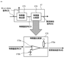
- FIG. 9 is a configuration diagram showing an example of the feature comparison unit 172, which is part of the anomaly detection unit 17 in the noise filter 100 according to the first embodiment.
- the feature comparison unit 172 generates an anomaly detection signal AS by performing a predetermined calculation on the feature signal CV output by the feature detection unit 171, and outputs the generated anomaly detection signal AS.
- FIG. 9 shows an example of the noise filter 100 according to the first embodiment, in which the feature comparison unit 172 is configured using a comparator circuit that compares the feature signal CV with a preset threshold voltage.
- the feature comparison unit 172 includes a comparator 172a, a DC voltage source 172b, and a pull-up resistor 172c.
- the inverting input terminal of the comparator 172a is connected to the input terminal side of the feature comparison unit 172 (left side of FIG. 9).
- the non-inverting input terminal of the comparator 172a is connected to the positive electrode of the DC voltage source 172b.
- the negative electrode of the DC voltage source 172b is grounded.
- the output terminal of the comparator 172a is connected to the output terminal side of the feature comparison unit 172.
- the pull-up resistor 172c is connected between the output terminal of the comparator 172a and the output terminal of the feature comparison unit 172.
- the voltage of the feature signal CV is compared with the voltage of the DC voltage source 172b, and an abnormality detection signal AS is output according to the result of the comparison. Specifically, for example, if the voltage of the feature signal CV is greater than the voltage of the DC voltage source 172b, an abnormality is detected and the abnormality detection signal AS is output as an ON signal. In this case, the voltage value of the DC voltage source 172b becomes the threshold voltage for determining whether or not an abnormality exists.
- the circuit that constitutes the feature comparison unit 172 is not limited to the example shown in FIG. 9, and can be freely configured within the scope of the present application.
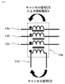
- FIG. 10 is a configuration diagram showing the cancellation signal injection unit 14 in the noise filter 100 according to the first embodiment.
- the cancellation signal injection unit 14 is composed of a common mode transformer.
- the common mode transformer constituting the cancellation signal injection unit 14 is hereinafter referred to as the injection transformer 14g.
- the injection transformer 14g includes an R-phase winding 14a wound around the R-phase power line, an S-phase winding 14b wound around the S-phase power line, a T-phase winding 14c wound around the T-phase power line, and an injection winding 14d.
- the R-phase winding 14a, the S-phase winding 14b, and the T-phase winding 14c are wound in the same phase.
- the injection transformer 14g configured as described above has a high inductance value only for the common mode and functions as a common mode choke coil.
- the cancellation signal injection unit 14 which is composed of the injection transformer 14g as described above, when the cancellation signal CS is input to both ends of the injection winding 14d, an induced voltage V that cancels the common mode noise CN is induced in the R-phase winding 14a, the S-phase winding 14b, and the T-phase winding 14c by the cancellation signal CS input to the injection winding 14d.
- the hardware configuration for realizing the control system according to the first embodiment may be configured with analog circuits as shown in Figures 8 and 9, but here we will explain an example that is different from analog circuits.
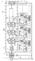
- FIG. 11 is an example of a hardware configuration diagram realizing the control system of the noise filter 100 according to the first embodiment.
- the "control system” here refers to the overall control of the noise filter 100, particularly including the control power supply 19.
- the control system of the noise filter 100 according to the first embodiment is mainly composed of a processor 71, a memory 72 as a main storage device, an auxiliary storage device 73, and an interface 74.
- the processor 71 is composed of, for example, a CPU (Central Processing Unit), an ASIC (Application Specific Integrated Circuit), a DSP (Digital Signal Processor), an FPGA (Field Programmable Gate Array), etc.
- a CPU Central Processing Unit
- ASIC Application Specific Integrated Circuit
- DSP Digital Signal Processor
- FPGA Field Programmable Gate Array
- Memory 72 is composed of a volatile storage device such as a random access memory, and auxiliary storage device 73 is composed of a non-volatile storage device such as a flash memory or a hard disk.
- a specific program executed by processor 71 is stored in auxiliary storage device 73.
- Processor 71 reads and executes this program as appropriate to perform various arithmetic processing. At this time, the above-mentioned specific program is temporarily saved from auxiliary storage device 73 to memory 72, and processor 71 reads the program from memory 72.
- the various types of arithmetic processing of the control system of the noise filter 100 and power conversion system 500 according to the first embodiment are realized by the processor 71 executing a predetermined program as described above.
- the results of the arithmetic processing by the processor 71 are temporarily stored in the memory 72, and are then stored in the auxiliary storage device 73 according to the purpose of the executed arithmetic processing.
- the control system may be realized by using either analog circuits or digital circuits.
- the following describes problems that may occur when an abnormality occurs in the control device of the noise filter 100, such as a temporary command value abnormality in the power conversion device 80 (the controlled device), an abnormality in the winding of the injection coil, or a component failure such as the transistor of the control circuit or the power supply capacitor.
- an abnormality occurs in the control device of the noise filter 100, such as a temporary command value abnormality in the power conversion device 80 (the controlled device), an abnormality in the winding of the injection coil, or a component failure such as the transistor of the control circuit or the power supply capacitor.
- the injection transformer 14g behaves as a common mode choke coil with the same number of turns in the main winding, and has a large inductance component.
- the resonant frequency between the injection transformer 14g and the load common mode capacitance fluctuates.
- the resonant frequency between the injection transformer 14g and the load common mode capacitance fluctuates, the resonant frequency of the fluctuated common mode path overlaps with the switching frequency of the power conversion device 80 and the band of its harmonic frequencies, which may instead cause a sudden increase in common mode noise CN.
- common mode noise CN it is necessary to increase the inductance component of the injection transformer 14g during protective operation by selecting a large number of turns for the injection transformer 14g so that the resonant frequency during protective operation is already lower than the switching frequency.
- increasing the number of turns for the injection transformer 14g undesirably increases the size of the noise filter 100.
- the common mode voltage share on the load side as viewed from the power conversion device 80, which is the noise source, is shared by the impedance ratio of the main circuit unit 101 shown in Fig. 4.
- the connection between the cancellation signal generation unit 16 and the cancellation signal injection unit 14 is cut off, the low output impedance of the cancellation signal generation unit 16 is no longer connected to the auxiliary winding connected to the control circuit side of the injection transformer 14g, and so the insertion impedance of the injection transformer 14g that constitutes the cancellation signal injection unit 14, which is part of the main circuit unit 101, increases significantly.
- the common mode voltage that the injection transformer 14g passively bears of the common mode noise CN shown in FIG. 3 increases significantly, which may cause magnetic saturation in the core. Magnetic saturation can cause problems such as heat generation, noise, and vibration, so it is necessary to avoid magnetic saturation, but an increase in the size of the core undesirably leads to an increase in the size of the noise filter 100.
- Figure 12A is a diagram explaining the behavior of the injection transformer 14g in the noise filter 100 according to embodiment 1 during normal operation
- Figure 12B is a diagram showing the relationship between the impedance and frequency during normal operation of the injection transformer 14g in the noise filter 100 according to embodiment 1.
- a cancellation signal generating unit 16 with low output impedance is connected to the injection winding 14d of the injection transformer 14g, and the cancellation signal injection unit 14 injects the cancellation signal CS into the electrical circuit 11.
- the insertion impedance in the common mode path of the injection transformer 14g is suppressed to a low value corresponding to the impedance of the amplifier circuit. Therefore, in the frequency band in which common mode noise CN occurs, there is no effect on the resonant frequency of the common mode path, and since the voltage sharing due to the common mode voltage is also low, magnetic saturation of the injection transformer 14g due to voltage sharing due to passive impedance does not occur.
- Figure 13A is a diagram explaining the behavior of the injection transformer 14g during protection operation in the noise filter 100 according to embodiment 1
- Figure 13B is a diagram showing the relationship between impedance and frequency during protection operation of the injection transformer 14g in the noise filter 100 according to embodiment 1.
- the injection winding 14d is open during protection operation. In other words, a high open impedance is connected to the injection winding 14d.
- the injection transformer 14g has an inductance component as a common mode choke coil corresponding to the core permeability, magnetic path length, cross-sectional area, and number of turns of the injection transformer 14g, and therefore behaves as an inductive impedance due to the inductance component, which greatly affects the resonance frequency of the common mode path. Furthermore, the voltage distribution resulting from the common mode voltage also increases significantly in the band where the common mode noise CN occurs, and as described above, there is a risk of magnetic saturation of the injection transformer 14g.
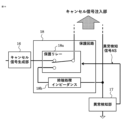
- FIG. 14 is a configuration diagram showing the protection circuit 18 of the noise filter 100 according to the first embodiment.
- the protection relay 18a constituting the protection circuit 18 can switch between two states by switching the relay contacts based on the abnormality detection signal AS: a noise cancellation operation state in which the cancellation signal injection unit 14 and the cancellation signal generation unit 16 are connected, and a noise cancellation stop state in which the cancellation signal injection unit 14 and the cancellation signal generation unit 16 are disconnected and the cancellation signal injection unit 14 is connected to the termination processing impedance 18b.
- the protective relay 18a is shown as a single C-contact relay, but it may be configured by combining different A-contact and B-contact relays, and may be configured as semiconductor relays as well as mechanical relays.
- the logic of the connected protective relay 18a may be such that a normally open contact is connected to the cancellation signal generating unit 16 and a normally closed contact is connected to the termination processing impedance 18b, or vice versa.
- the feature detection unit 171 outputs the effective voltage value of the output voltage of the cancellation signal CS as the feature signal CV. Furthermore, the DC voltage source 172b of the feature comparison unit 172 uses the output voltage value of the cancellation signal CS as the threshold voltage when determining whether or not there is an abnormality. In other words, the output voltage value of the DC voltage source 172b is the threshold voltage Vth of the effective voltage value. As a result, the feature comparison unit 172 compares the effective voltage value of the output voltage of the cancellation signal CS with the threshold voltage Vth of the effective voltage value.
- the output of the comparator 172a becomes high, and the feature comparison unit 172 outputs the abnormality detection signal AS as ON.
- the output of the comparator 172a becomes low, and the feature comparison unit 172 outputs the abnormality detection signal AS as OFF.
- the abnormality detection signal AS output from the feature comparison unit 172 is input to the protection circuit 18.
- the protection circuit 18 is typically configured with a control relay of a contact C. Based on the abnormality detection signal AS, the protection circuit 18 disconnects the control power supply 19 from the cancellation signal output unit 13, cuts off the connection between the cancellation signal output unit 13 and the cancellation signal injection unit 14, and connects the cancellation signal injection unit 14 to the termination impedance 18b.
- This operation of the cancellation signal output unit 13 cuts off the injection of the cancellation signal CS into the electric circuit 11, so that the injection of the cancellation signal CS having an abnormal output waveform into the electric circuit 11 can be prevented, and the resonance frequency fluctuation of the common mode path due to the insertion impedance fluctuation of the injection transformer 14g constituting the cancellation signal injection unit 14 and the occurrence of core magnetic saturation of the injection transformer 14g are suppressed.
- the abnormality detection unit 17 detects an abnormality and causes the protection circuit 18 to perform a cutoff operation
- the feature comparison unit 172 outputs an off-output of the abnormality detection signal AS
- the cutoff operation of the protection circuit 18 will be reset and the generation and injection of the cancellation signal CS will be restored.
- a delay circuit or counter circuit may be used to perform the recovery operation after a preset time has elapsed.
- an example of a circuit using operational amplifier 16b as the configuration of cancellation signal generation unit 16 is shown, but the configuration of cancellation signal generation unit 16 may be, for example, another inverting amplifier circuit or a non-inverting amplifier circuit.
- protection circuit 18 performs a cut-off operation in response to abnormality detection signal AS, but it is also possible to perform operations other than a simple cut-off operation by combining it with a logic circuit, such as latching the cut-off operation or being able to release the cut-off operation by combining it with a reset circuit.
- a circuit using an operational amplifier as the configuration of the feature detection unit 171
- it may be a circuit of another configuration that achieves the same purpose, for example.
- an example of using an effective voltage value as the detection quantity used by the feature detection unit 171 has been shown
- the feature detection unit 171 may be configured to detect a different value, such as an instantaneous value or an average value, as the feature.
- a circuit using a comparator 172a as the configuration of the feature comparison unit 172 it may be a different circuit that achieves the same purpose, for example.
- noise filter 100 in addition to the noise detection unit 12 and the cancellation signal injection unit 14, another common mode choke coil may be connected to the electrical path 11. Also, the noise detection unit 12 may be configured using a capacitor instead of a common mode transformer.
- the noise filter 100 is characterized in that it executes a process when an abnormality occurs in the cancellation signal CS, that is, an abnormality processing sequence.
- the abnormality processing sequence refers to the following sequence. (1) A sequence in which the protection circuit 18 is operated based on the abnormality detection signal AS, the injection of the cancellation signal CS into the electric circuit is cut off, and both ends of the cancellation signal injection unit 14 are connected to the termination impedance 18b. (2) A sequence in which the power conversion device 80 judges an abnormality based on the abnormality detection signal AS, and varies the switching frequency based on the resonance frequency predicted by the prediction calculation unit provided in the power conversion device 80.
- the abnormality processing sequence is, for example, any one of the above sequences (1) to (3). Details of the sequences (2) and (3) will be described in the sixth embodiment described later. It should be noted that the sequences listed above are merely examples of abnormality processing sequences, and needless to say, other processing that is effective in the event of an abnormality is also included.
- the noise filter 100 and power conversion system 500 according to the first embodiment operate stably even when an abnormality occurs in the cancellation signal, thereby achieving high reliability.
- an abnormality detection unit that detects abnormalities in the noise filter and power conversion device based on the output voltage or output current of the cancellation signal and outputs an abnormality detection signal
- a protection circuit that cuts off the connection between the cancellation signal injection unit and the cancellation signal output unit based on the abnormality detection signal and connects the cancellation signal injection unit to the termination processing impedance
- the abnormality is detected from a change in the output voltage or output current of the cancellation signal caused by the abnormal state, and the output of the cancellation signal from the cancellation signal output unit to the cancellation signal injection unit is suppressed, preventing the injection of the abnormal cancellation signal into the electrical circuit, and by connecting the termination impedance to the auxiliary winding of the injection transformer that constitutes the cancellation signal injection unit, an increase in common mode noise due to unintended resonance caused by fluctuations in the resonance frequency of the common mode path, or magnetic saturation due to an unintended increase in the insertion impedance of the injection transformer, can be prevented, thereby achieving a highly reliable noise
- FIG. 15 is a configuration diagram showing a noise filter 100a according to the second embodiment. Differences from the first embodiment will be mainly described.
- the cancellation signal injection unit 14 that injects the cancellation signal CS output from the cancellation signal output unit 13 into the electric circuit 11
- a plurality of cancellation signal injection units are provided and connected in series and parallel. This is because, when the noise filter 100a is provided between a large-capacity power conversion device and a load, in particular, it may be advantageous to configure the cancellation signal injection unit 14 in a divided manner due to problems with core implementation.
- FIG. 15 shows a configuration in which the cancellation signal injection section has three in series and two in parallel.
- the cancellation signal injection section 14 is composed of cancellation signal injection sections 14A1, 14A2, and 14A3 provided on one of the parallel electric paths 11A, and cancellation signal injection sections 14B1, 14B2, and 14B3 provided on the other parallel electric path 11B.
- the cancellation signal output unit 13 includes a control power supply 19 that supplies the cancellation signal output unit 13 with power for generating and injecting the cancellation signal CS, and a protection circuit 18 that is inserted between the control power supply 19 and the cancellation signal output unit 13 and that suppresses the injection of the cancellation signal CS into the electrical circuits 11A, 11B during protection operation and can be connected to the termination impedance 18b.
- the cancellation signal output unit 13 is provided for each unit of the number of cancellation signal injection units 14 in series.
- the noise filter 100a includes the same number of cancellation signal output units 13 as the number of cancellation signal injection units 14 in series.
- the noise filter 100a is configured with multiple cancellation signal injection sections, with the multiple cancellation signal injection sections arranged in series further arranged in parallel with respect to the electrical path, with the number of multiple cancellation signal injection sections being the same between the parallel sections.
- noise filter 100a configured as shown in FIG. 15, when a protection operation occurs in cancellation signal output unit 13, the protection operation is performed on cancellation signal injection units 14A1 and 14B1, and they are connected to the termination impedances 18b provided in each. In this case, the number of cancellation signal injection units 14 inserted between electrical paths 11A and 11B is maintained the same.
- FIG. 16 is a configuration diagram showing a noise filter 100b, which is another example of a noise filter according to embodiment 2. The differences from embodiment 1 and noise filter 100a according to embodiment 2 shown in FIG. 15 will be mainly described.
- the cancellation signal injection unit 14 that injects the cancellation signal CS output from the cancellation signal output unit 13 into the electrical circuit 11 is provided with a plurality of cancellation signal injection units that are connected in series and parallel.
- the cancellation signal injection unit 14 of the noise filter 100b has a configuration in which the number of series is N and the number of parallel connections is 2, similar to the configuration shown in FIG. 15.
- the noise filter 100b is composed of cancellation signal injection units 14A1, 14A2, 14A3, ... 14AN provided on one of the parallel electric paths 11A, and cancellation signal injection units 14B1, 14B2, 14B3, ... 14BN provided on the other parallel electric path 11B.
- the number of series, N may be determined appropriately based on the characteristics required for the noise filter 100b and the characteristics required for the power conversion system.
- the cancellation signal output unit 13 has a control power supply 19 that supplies the cancellation signal output unit 13 with power for generating and injecting the cancellation signal CS, and a protection circuit 18 that is inserted between the control power supply 19 and the cancellation signal output unit 13 and that suppresses the injection of the cancellation signal CS during protection operation and can be connected to a termination impedance 18b.
- N cancellation signal output units 13 are provided, which is the same number as the number of cancellation signal injection units 14 in series.
- the abnormality detection signal AS from the abnormality detection unit 17 in the cancellation signal output unit 13 connected to the cancellation signal injection unit 14A1 of one of the parallel electric circuits 11A is also input to the cancellation signal injection unit 14B1.
- the abnormality detection signal AS from the abnormality detection unit 17 in the cancellation signal output unit 13 connected to the cancellation signal injection unit 14B1 of the other parallel electric circuit 11B is also input to the cancellation signal injection unit 14A1.
- a similar configuration is arranged up to the combination of the cancellation signal injection unit 14AN and the cancellation signal injection unit 14BN.
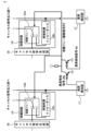
- FIG. 17 shows an example of the configuration of the exchange of the abnormality detection signal AS between the cancellation signal output units 13 in the noise filter 100a shown in FIG. 15 and the noise filter 100b shown in FIG. 16.
- the abnormality detection signal AS output from the abnormality detection unit 17 is input to a wired-OR connected transistor circuit, for example, via a base resistor, and bundled into a single protection relay drive signal RY, which simultaneously switches the protection relays 18a of the two cancellation signal output units.
- the cancellation signal injection section is configured to be divided into a plurality of sections, so that an effect is achieved in that high reliability can be achieved even when the noise filter is provided between a large-capacity power conversion device and a load.
- Embodiment 3 A noise filter 100d and a power conversion system 500d according to the third embodiment will be described with reference to FIGS. 18 is an overall configuration diagram showing a power conversion system 500d according to embodiment 3.
- the power conversion system 500d includes a power conversion device 80 that is disposed between an AC power source 1 and a load 90 and converts input power from the AC power source 1 into any DC power or AC power, and a noise filter 100d inserted between the AC power source 1 and the power conversion device 80.
- the AC power source 1 and the noise filter 100d are connected by an electric path 2, and the noise filter 100d, the power conversion device 80, and the load 90 are connected by an electric path 11.
- the electric circuit 11 is connected to the electric circuit 2 of the AC power source 1, and the input power from the AC power source 1 is input to the power conversion device 80 via the electric circuit 2.
- the power conversion device 80 converts the power input from the AC power source 1 into power required to drive the load 90 and outputs it.
- the noise filter 100d is disposed between the AC power source 1 and the power conversion device 80, but it may be disposed between the power conversion device 80 and the load 90.
- FIG. 19 is a diagram for explaining common mode noise CN generated in a power conversion system 500d according to the third embodiment, showing a common mode equivalent circuit.
- the AC power source 1 and the load 90 are connected on the ground side by a ground wire 3 in addition to the above-mentioned electric circuit 11.
- the noise filter 100d is provided with a ground capacitor 15, one end of which is connected to the ground wire 3.
- a parasitic capacitance 86 and a parasitic capacitance 91 exist between the power conversion device 80 and the ground wire 3, and between the load 90 and the ground wire 3, respectively.
- a common mode voltage Vcn of the power conversion device 80 is applied to the common mode loop via the parasitic capacitances 86, 91, and the ground wire 3, and a common mode current (common mode noise CN) flows as shown by the arrow in FIG. 19.
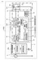
- FIG. 20 is a configuration diagram showing a noise filter 100d according to the third embodiment.
- the noise filter 100d is inserted between the AC power supply 1 and the power conversion device 80.
- the noise filter 100d includes a noise detection unit 12 provided on the electric circuit 11 connected to the electric circuit 2, a cancellation signal output unit 13 that generates and outputs a cancellation signal CS from the common mode noise CN (not shown in FIG.
- a cancellation signal injection unit 14 that is provided on the electric circuit 11 closer to the output end than the noise detection unit 12, i.e., on the power conversion device 80 side, and injects the cancellation signal CS output from the cancellation signal output unit 13 into the electric circuit 11, a control power supply 19 that supplies power to the cancellation signal output unit 13 for generating and injecting the cancellation signal CS, and a protection circuit 18 that is inserted between the control power supply 19 and the cancellation signal output unit 13 and can cut off the supply of power from the control power supply 19.
- the noise filter 100d includes a protection circuit 18 that can cut off the connection between the cancellation signal output unit 13 and the cancellation signal injection unit 14 as a protection means for preventing an abnormal cancellation signal CS from being injected into the electrical circuit 11.
- the noise filter 100d according to the third embodiment differs from the noise filters according to the first and second embodiments in that it constitutes a feedback control system.
- a feedback control system has the advantage of being more robust against impedance errors in the controlled object than a feedforward system.
- a ground capacitor 15 connected between the electric circuit 11 and the ground wire 3 is provided, and the noise detection unit 12, the cancellation signal injection unit 14, and the ground capacitor 15 constitute a main circuit unit 101d in the power conversion system 500d.
- a filter unit 20 is provided between the noise detection unit 12 and the cancellation signal generation unit 16. The filter unit 20 adjusts the characteristics of the cancellation signal CS by adjusting the noise detection signal DS.
- the control characteristics of the noise filter 100d depend heavily on the main circuit section 101d.
- the inductance value of the main circuit section 101d is the sum of the inductance value of the common mode transformer that constitutes the noise detection section 12 and the inductance value of the injection transformer 14g that constitutes the cancellation signal injection section 14.
- the capacitance value of the main circuit section 101d is the capacitance value of the ground capacitor 15. The control characteristics of the main circuit section 101d will be described in detail later.
- Figures 21A, 21B, and 21C are diagrams showing the control response of the main circuit section 101d of the noise filter 100d according to embodiment 3.
- Figure 21A is a diagram showing the control response when there is no filter section 20
- Figure 21B is a diagram showing the pass characteristics of the filter section 20
- Figure 21C is a diagram showing the control response when there is a filter section 20.
- the horizontal axis is frequency and the vertical axis is gain.
- control response refers to the open-loop response in the path that starts from the output of the noise detection unit 12, passes through the cancellation signal output unit 13 and the cancellation signal injection unit 14, and returns to the noise detection unit 12.
- the control stability of the noise filter 100d depends on the values of the gain margin and phase margin of the open-loop response.
- the noise filter in the open loop response of the noise filter without the filter unit 20, a large resonance peak occurs at the resonance frequency f1 of the main circuit unit 101d, and the gain increases rapidly. Although not shown in FIG. 21A, phase rotation also occurs at the resonance frequency f1. In this way, without the filter unit 20, the noise filter has an unstable control response at the resonance frequency f1. If the common mode noise CN detected by the noise detection unit 12 contains a component of the resonance frequency f1, the cancellation signal CS may also become unstable.
- L1 is the inductance value of the main circuit unit 101d
- C1 is the capacitance value of the main circuit unit 101d.
- a filter section 20 having the filter pass characteristic shown in FIG. 21B is provided between the noise detection section 12 and the cancellation signal generation section 16.
- the filter section 20 is configured so that its reject frequency matches the resonance frequency f1 of the main circuit section 101d.
- Such a filter section 20 can be realized, for example, by a notch filter.
- the filter section 20 when the filter section 20 is provided between the noise detection section 12 and the cancellation signal generation section 16, even if the common mode noise CN detected by the noise detection section 12 contains a component of the resonance frequency f1, it is possible to generate a cancellation signal CS in which the resonance peak is attenuated. As a result, the noise filter 100d can exert a stable noise suppression effect.
- FIG. 22A and 22B are diagrams showing the control response of the noise filter 100d according to embodiment 3, with FIG. 22A showing the gain characteristic and FIG. 22B showing the phase characteristic.
- the control response characteristic (control characteristic) of the noise filter 100d the phase rotates due to the phase delay of the main circuit section 101d, the cancellation signal generating section 16, and the filter section 20.
- a notch filter and a low-pass filter are combined as the filter section 20 of the noise filter 100d to suppress the resonance peak at the resonance frequency f1 as described above, and the gain margin G2 at the phase inversion frequency f2 in the low frequency band and the gain margin G3 at the phase inversion frequency f3 in the high frequency band are set to values that ensure control stability.
- the gain margins G2 and G3 are indicated by upward arrows when they have positive values and by downward arrows when they have negative values.
- the value that ensures control stability is, for example, 6 dB.
- FIGS. 23A and 23B are diagrams showing the control response when a change in the control characteristics occurs due to the occurrence of an abnormality in the noise filter 100d according to embodiment 3, with FIG. 23A showing the change in gain characteristics and FIG. 23B showing the change in phase characteristics. Note that, in order to compare normal and abnormal conditions, the gain and phase characteristics in normal conditions are shown by solid lines, and the gain and phase characteristics in abnormal conditions are shown by dashed lines. Here, an example is shown as an "abnormality" in which the phase inversion frequency f3 in the high frequency band has changed to frequency f3*.
- a typical example of such an abnormality is when a component failure or other factor causes the low-pass filter to lose its function, resulting in a change in the characteristics of the filter section.
- the value of the gain margin G3 at the phase inversion frequency f3 in the high-frequency band fluctuates and may deviate from a value that ensures control stability.
- the gain margin at the high-frequency phase inversion frequency f3 fluctuates to a negative gain margin G3*. This indicates that the control response of the noise filter 100d is unstable.
- the cancellation signal CS output from the cancellation signal output unit 13 also becomes an unstable signal with an abnormal output waveform, and an abnormal and unstable cancellation signal CS is injected into the electrical circuit 11.
- FIG. 24 is a diagram showing an abnormal output waveform of the cancellation signal output unit 13 according to embodiment 3, showing an example of the waveform of the cancellation signal CS when an abnormality occurs.
- the horizontal axis represents time. Because the gain margin at the phase inversion frequency f3 is a negative value, the frequency component of the phase inversion frequency f3 continues to be amplified as shown in FIG. 24, causing oscillation. Note that the section between the arrow and the dashed line in FIG. 24 indicates the period T3 of the cancellation signal CS when an abnormality occurs. Period T3 is equal to the reciprocal of the phase inversion frequency f3.
- the noise source of the common mode noise CN also appears in the noise filter 100d.
- the load 90, the system, and the power conversion device 80 share the noise source voltage according to their respective impedance ratios.
- the cancellation signal injection unit 14 of the noise filter 100d according to the third embodiment is composed of an injection transformer 14g.
- the injection transformer 14g constituting the cancellation signal injection unit 14 is an inductive load with an inductive impedance for the cancellation signal output unit 13, and therefore has a high impedance in the high frequency band.
- the cancellation signal output unit 13 does not immediately produce phenomena that would affect the specifications of the circuit components, such as overvoltage or overcurrent. This means that since it is not possible to detect an abnormality in the noise filter, even if the noise filter is equipped with an overvoltage protection circuit or overcurrent protection circuit, the protection function will not stop the noise filter.
- the abnormality detection unit 17 detects an abnormality, and when an abnormality is detected, the protection circuit 18 is operated to stop the injection of the cancellation signal CS and connect the termination impedance 18b to the cancellation signal injection unit 14, thereby simultaneously solving the problem of constructing a feedback control system.
- the protection circuit 18 is operated to stop the injection of the cancellation signal CS and connect the termination impedance 18b to the cancellation signal injection unit 14, thereby simultaneously solving the problem of constructing a feedback control system.
- FIG. 25A shows the waveform of the common mode voltage under normal conditions
- FIG. 25B shows the waveform of the common mode current under normal conditions
- FIG. 25C shows the waveform of the output voltage of the cancellation signal CS under normal conditions for the noise filter 100d according to embodiment 3
- FIG. 25D shows the waveform of the output current of the cancellation signal CS under normal conditions.
- the horizontal axis represents time.
- the common mode voltage is the voltage of the common mode noise CN.
- the common mode current is the current that flows in the electrical circuit 11 due to the common mode voltage.
- the common mode current is the current that flows in the electrical circuit 11 when a common mode voltage is input to the common mode equivalent circuit shown in FIG. 19 and when it is assumed that the noise filter 100d is not present.
- the common mode voltage is generated by the switching operation of each semiconductor switch that constitutes the power conversion device 80 shown in FIG. 2, and has a rectangular waveform as shown in FIG. 25A.
- the common mode current has a spike-like waveform as shown in FIG. 25B, and causes noise problems at various points along the path.
- the noise detection unit 12 of the noise filter 100d detects the common mode current and transmits a noise detection signal DS to the cancellation signal output unit 13, which generates a cancellation signal CS from the noise detection signal DS.
- the cancellation signal CS is injected into the electrical circuit 11 via the cancellation signal injection unit 14.
- the output voltage of the cancellation signal CS under normal conditions has a spike-like waveform as shown in Figure 25C.
- the output current of the cancellation signal CS generated by the output voltage of the cancellation signal CS also has a spike-like waveform as shown in Figure 25D.
- the output current of the cancellation signal CS is a current that cancels out the common mode current, and so, like the common mode current, it has the characteristic of having a waveform whose effective value is extremely smaller than the peak value.
- the noise current flowing out from the power conversion device 80 which is the noise source of the common mode noise CN, passes through the cancellation signal injection unit 14, causing a disturbance component to be superimposed on the output current of the cancellation signal CS, and the disturbance component is also superimposed on the output voltage of the cancellation signal CS due to the product of the output impedance and current of the cancellation signal CS.
- the superimposition of disturbance components as described above is ignored in Figures 25C and 25D.
- FIG. 26A shows the waveform of the common mode voltage when an abnormality occurs
- FIG. 26B shows the waveform of the common mode current when an abnormality occurs
- FIG. 26C shows the waveform of the output voltage of the cancellation signal CS when an abnormality occurs in the noise filter 100d according to embodiment 3
- FIG. 26D shows the waveform of the output current of the cancellation signal CS when an abnormality occurs.
- the horizontal axis represents time.
- An abnormal output waveform does not have the characteristic of a normal waveform, that is, the characteristic of the effective value being extremely smaller than the peak value.
- the effective voltage value of the output voltage of the cancellation signal CS is 1/ ⁇ 2 times the voltage peak value, and there is no large difference between the peak value and the effective value.
- the effective current value of the output current of the cancellation signal CS is 1/ ⁇ 2 times the current peak value, and there is no significant difference between the peak value and the effective value. This is also true when the output voltage of the operational amplifier becomes saturated due to high-gain oscillation operation, causing the output voltage waveform of the cancellation signal CS to become rectangular.
- the effective voltage value of the output voltage of the cancellation signal CS and the effective current value of the output current are larger than in a normal state.
- the effective voltage value of the output voltage of the cancellation signal CS can be used as the criterion for determining an abnormality.
- an appropriate threshold voltage or threshold current can be set, and by comparing the actual effective voltage value with the threshold voltage or the actual effective current value with the threshold current, it can be determined whether the noise filter 100d is operating normally, i.e., whether the noise filter 100d is able to cancel the common mode current, or whether it has fallen into an abnormal operation for some reason.
- the threshold voltage of the effective voltage value for determining whether or not there is an abnormality is Vth
- the effective voltage value during abnormal operation is V2
- the presence or absence of an abnormality can be determined by selecting the threshold voltage Vth for the effective voltage value such that V1 ⁇ Vth ⁇ V2.
- the effective current value of the output current of the cancel signal CS is used to determine whether or not there is an abnormality.
- the noise filter according to the third embodiment has an effect of achieving high reliability even when the noise filter constitutes a feedback control system.
- the abnormality when an abnormality occurs in the noise filter that requires protection, the abnormality is detected from a change in the output voltage or output current of the cancellation signal CS due to the abnormality, and the output of the noise cancellation signal from the cancellation signal output unit to the cancellation signal injection unit is suppressed, preventing the injection of the abnormal cancellation signal into the electrical circuit.
- a termination impedance to the auxiliary winding of the injection transformer that constitutes the cancellation signal injection unit, an increase in common mode noise CN due to unintended resonance caused by fluctuations in the resonance frequency of the common mode path, or magnetic saturation due to an unintended increase in the insertion impedance of the injection transformer, is prevented, thereby achieving high reliability.
- an abnormality in the noise filter is detected based on the output voltage or output current of the cancellation signal CS, an abnormality in the noise filter in the high frequency band can be reliably detected even if the cancellation signal injection section of the cancellation signal CS is configured with an inductance load such as a common mode transformer (injection transformer).
- an inductance load such as a common mode transformer (injection transformer).
- the generation and injection of the cancellation signal CS is stopped by the protection circuit when an abnormality is detected, stable operation can be achieved while setting the gain margin and phase margin for suppressing controlled oscillation in the feedback control system lower than before.
- the ability to set the gain margin and phase margin lower than before means that the control gain of the noise filter can be improved, which has the effect of improving the amount of noise suppression.
- FIG. 27 is a configuration diagram showing a noise filter 100e and a power conversion system 500e according to a fourth embodiment.
- the noise filters according to the first, second, and third embodiments all include a protection circuit 18 that performs an operation of disconnecting the cancellation signal injection unit 14 from the cancellation signal output unit and connecting the cancellation signal injection unit 14 to the termination processing impedance 18b in response to an abnormality detection signal AS.
- the noise filter 100e according to the fourth embodiment has a function of notifying the power conversion device 80, which is the noise source, of an abnormality in the noise filter 100e, instead of the above-mentioned protection circuit 18. Therefore, the protection circuit 18 is not an essential component of the noise filter 100e according to the fourth embodiment.
- an abnormal state signal output unit 21 is provided in the cancellation signal output unit 13, and the abnormality detection signal AS output by the abnormality detection unit 17 is input to the abnormal state signal output unit 21.
- the noise filter 100e according to the fourth embodiment has the abnormal state signal output unit 21 as a protection means for preventing an abnormal cancellation signal CS from being injected into the electric circuit 11.
- the abnormal state signal output unit 21 has an output circuit capable of outputting a signal to the power conversion device 80, and when the abnormality detection signal AS is input, it outputs an abnormal state signal AS2 to the power conversion device 80.
- the abnormal state signal AS2 is typically a differential signal that is resistant to external disturbances or a low-impedance current signal, and is generated based on the abnormality detection signal AS. Furthermore, the abnormal state signal AS2 is isolated from the control potential of the noise filter 100e as necessary.
- the power conversion device 80 which receives the abnormal state signal AS2, recognizes that the noise filter 100e is in an abnormal state.
- the power conversion device 80 which recognizes that the noise filter 100e is in an abnormal state, takes measures such as stopping operation depending on the nature of the abnormality, for example using a predictive calculation unit (not shown).
- a control circuit that stops the power conversion device 80 based on the abnormal state signal AS2 may be provided outside or inside the power conversion device 80. Such a control circuit receives the abnormal state signal AS2 and transmits a stop command to the power conversion device 80 as necessary.
- the noise filter according to the fourth embodiment is provided with the abnormal state signal output section, and therefore has the effect of providing a highly reliable noise filter.
- the noise filter according to the fourth embodiment differs from the first, second, and third embodiments in that it does not directly address problems such as fluctuations in the common mode resonant frequency due to fluctuations in the insertion impedance of the injection transformer 14g during protective operation and core magnetic saturation of the injection transformer 14g.
- the abnormal state signal is used to make the power conversion device, which is the noise source of the common mode noise CN, aware of an abnormality in the noise filter.
- the power conversion device takes measures such as stopping operation as necessary, so that stopping the noise source of the common mode noise CN has the effect of preventing an abnormal cancellation signal from being generated and injected into the electrical circuit, or an increase in the common mode noise CN due to an unintended common mode resonant frequency.
- the noise filter according to the fourth embodiment has the effect of realizing high reliability as a noise filter by indirectly preventing an abnormal cancellation signal CS from being injected into the electrical circuit or an unintended increase in common mode noise CN by making the power conversion device 80, which is the noise source, aware of an abnormality in the noise filter.
- the noise filter 100e according to the fourth embodiment may be combined with the protection circuit 18 of the noise filter according to the first, second, and third embodiments. Since the noise filter 100e according to the fourth embodiment outputs the abnormal state signal AS2 to the noise source of the common mode noise CN, if there is another controlled device that is a noise source of the common mode noise CN, the noise filter 100e may be configured to output the abnormal state signal AS2 to the other controlled device as well.
- Embodiment 5. 28 is a configuration diagram showing a management system 1000 according to embodiment 5.
- the management system 1000 includes a power conversion system 500f and a management device 200.
- the power conversion system 500f is composed of a power conversion device 80 that is disposed between an AC power source 1 and a load 90 and converts input power from the AC power source 1 into any DC power or AC power, a load 90 to which any DC power or AC power is supplied from the power conversion device 80, and a noise filter 100f having a communication function that is provided on an electric circuit 11 that connects the power conversion device 80 and the load 90.
- the noise filter 100f may also be provided on an electric circuit 2 that connects the AC power source 1 and the power conversion device 80.
- a DC power source may be used instead of the AC power source 1.
- FIG. 29 is a configuration diagram showing a noise filter 100f with a communication function, which is applied to a power conversion system 500f according to embodiment 5.
- the power conversion system 500f according to embodiment 5 differs in configuration from the noise filter 100 according to embodiment 1 in that the noise filter 100f includes a communication unit 24 connected to the cancellation signal output unit 13.
- the communication unit 24 which is part of the configuration of the noise filter 100f, converts various signals generated inside the cancellation signal output unit 13, such as the cancellation signal CS and the abnormality detection signal AS, into digital data and transmits the data to the outside of the power conversion system 500f.
- the Internet may be used for transmission.
- the management device 200 constituting the management system 1000 includes a receiving unit 201, a database 202, a data analysis unit 203, and a transmitting unit 204, as shown in FIG. 28.
- the receiving unit 201 receives data transmitted to the outside of the power conversion system 500f via the communication unit 24 of the noise filter 100f, and stores the data in the database 202.
- the receiving unit 201 can also simultaneously receive data transmitted from each of the power conversion systems 500f owned by multiple clients.
- the database 202 sequentially stores the data transmitted from the power conversion system 500f. Note that data transmitted separately from multiple power conversion systems 500f for different clients may be stored separately in areas in the database 202 designated for each client.
- the data analysis unit 203 performs various analyses of the tendency, frequency, and cause of abnormalities that occur in the power conversion system 500f based on the data stored in the database 202.
- One example of the analysis is to diagnose each part of the power conversion device 80, such as determining whether it is better to replace it since the power conversion device 80 has a high failure frequency.
- the transmission unit 204 transmits the analysis results of the data analysis unit 203 to an external device outside the management system 1000, for example, via the Internet.
- Examples of the transmission destination include the management system of a client that operates the power conversion system 500f.
- the abnormality detection unit 17 transmits an abnormality detection signal AS, and the protection circuit 18 operates to perform a protective operation by cutting off the connection between the cancellation signal generation unit 16 and the cancellation signal injection unit 14, thereby achieving high reliability in the power conversion system 500f.
- the management system 1000 according to the fifth embodiment is applied, the data transmitted from the power conversion system 500f to the management device 200 is analyzed by the data analysis unit 203, and it becomes possible to, for example, determine the cause of the abnormality and propose a method of dealing with the abnormality to resolve it, thereby eliminating the cause of the abnormality at an early stage, and thus the reliability of the power conversion system 500f is further improved.
- the management system 1000 it becomes possible to grasp the operating status of the power conversion system 500f remotely, which facilitates management and maintenance of the power conversion system 500f. Furthermore, for the client who operates the power conversion system 500f, the analysis results and countermeasures for abnormalities by the management device 200 can be easily obtained, for example, via the Internet, so that maintenance and inspection of the power conversion system 500f can be performed at the appropriate time, or the number of maintenance and inspections can be reduced, thereby simultaneously realizing labor savings.
- the management system 1000 has the management device 200 that performs data analysis using data transmitted from the power conversion system 500f. This makes it possible to quickly address the cause of an abnormality, thereby achieving the effect of further improving the reliability of the power conversion system 500. Furthermore, this also has the effect of improving the maintainability, such as the management and maintenance of the power conversion system.
- FIG. 30 is a configuration diagram showing the power conversion system 500g according to the sixth embodiment.
- the power conversion system 500g according to the sixth embodiment differs from the power conversion system 500 according to the first embodiment in that a power conversion device 80a includes a prediction calculation unit 181 and an abnormality estimation unit 182.
- the configuration of the noise filter 100 is the same as that of the first embodiment.
- the prediction calculation unit 181 of the power conversion device 80a recognizes that the noise filter 100 is in an abnormal state and outputs a resonant frequency prediction value based on the abnormality detection signal AS.
- the prediction calculation unit 181 can also take measures to vary the switching frequency based on the resonant frequency prediction value.
- the abnormality estimation unit 182 of the power conversion device 80a outputs an abnormality continuation judgment value if the abnormality detection signal AS continues for a preset period or longer. Furthermore, it is also possible to stop the operation of the power conversion device 80a based on the abnormality continuation judgment value.
- a prediction calculation unit and an abnormality estimation unit are provided inside the power conversion device, so that it is possible to respond to abnormal conditions on the power conversion device side as well, thereby achieving the effect of providing a highly reliable power conversion system.
Landscapes
- Engineering & Computer Science (AREA)
- Power Engineering (AREA)
- Inverter Devices (AREA)
- Power Conversion In General (AREA)
Priority Applications (3)
| Application Number | Priority Date | Filing Date | Title |
|---|---|---|---|
| CN202280100471.2A CN119968766A (zh) | 2022-10-07 | 2022-10-07 | 噪声滤波器、电力变换系统以及管理系统 |
| PCT/JP2022/037561 WO2024075267A1 (ja) | 2022-10-07 | 2022-10-07 | ノイズフィルタ、電力変換システム及び管理システム |
| JP2024555575A JP7814542B2 (ja) | 2022-10-07 | 2022-10-07 | ノイズフィルタ、電力変換システム及び管理システム |
Applications Claiming Priority (1)
| Application Number | Priority Date | Filing Date | Title |
|---|---|---|---|
| PCT/JP2022/037561 WO2024075267A1 (ja) | 2022-10-07 | 2022-10-07 | ノイズフィルタ、電力変換システム及び管理システム |
Publications (1)
| Publication Number | Publication Date |
|---|---|
| WO2024075267A1 true WO2024075267A1 (ja) | 2024-04-11 |
Family
ID=90607952
Family Applications (1)
| Application Number | Title | Priority Date | Filing Date |
|---|---|---|---|
| PCT/JP2022/037561 Ceased WO2024075267A1 (ja) | 2022-10-07 | 2022-10-07 | ノイズフィルタ、電力変換システム及び管理システム |
Country Status (3)
| Country | Link |
|---|---|
| JP (1) | JP7814542B2 (https=) |
| CN (1) | CN119968766A (https=) |
| WO (1) | WO2024075267A1 (https=) |
Families Citing this family (1)
| Publication number | Priority date | Publication date | Assignee | Title |
|---|---|---|---|---|
| CN120956045B (zh) * | 2025-10-14 | 2026-01-23 | 北京七星华创微电子有限责任公司 | 一种实现滤波处理的多路可控电源变换器及滤波处理方法 |
Citations (3)
| Publication number | Priority date | Publication date | Assignee | Title |
|---|---|---|---|---|
| JP2015126593A (ja) * | 2013-12-26 | 2015-07-06 | 株式会社東芝 | 漏れ電流抑制回路、太陽光発電システム及びモータ制御装置 |
| JP2017051085A (ja) * | 2015-09-01 | 2017-03-09 | 富士電機株式会社 | アクティブノイズ抑制装置 |
| WO2021166018A1 (ja) * | 2020-02-17 | 2021-08-26 | 三菱電機株式会社 | ノイズ抑制装置 |
-
2022
- 2022-10-07 JP JP2024555575A patent/JP7814542B2/ja active Active
- 2022-10-07 WO PCT/JP2022/037561 patent/WO2024075267A1/ja not_active Ceased
- 2022-10-07 CN CN202280100471.2A patent/CN119968766A/zh active Pending
Patent Citations (3)
| Publication number | Priority date | Publication date | Assignee | Title |
|---|---|---|---|---|
| JP2015126593A (ja) * | 2013-12-26 | 2015-07-06 | 株式会社東芝 | 漏れ電流抑制回路、太陽光発電システム及びモータ制御装置 |
| JP2017051085A (ja) * | 2015-09-01 | 2017-03-09 | 富士電機株式会社 | アクティブノイズ抑制装置 |
| WO2021166018A1 (ja) * | 2020-02-17 | 2021-08-26 | 三菱電機株式会社 | ノイズ抑制装置 |
Also Published As
| Publication number | Publication date |
|---|---|
| JP7814542B2 (ja) | 2026-02-16 |
| CN119968766A (zh) | 2025-05-09 |
| JPWO2024075267A1 (https=) | 2024-04-11 |
Similar Documents
| Publication | Publication Date | Title |
|---|---|---|
| US7944326B2 (en) | EMC filter | |
| US7659797B2 (en) | Low-leakage EMC filter | |
| US9013840B2 (en) | Adaptive line filter | |
| JP7814542B2 (ja) | ノイズフィルタ、電力変換システム及び管理システム | |
| CN112335163B (zh) | 无源滤波器电路电容器功能确定方法、确定装置和电设备 | |
| WO2023054660A1 (ja) | ノイズ低減回路、電力変換装置及び冷凍装置 | |
| JP7738675B2 (ja) | ノイズフィルタ | |
| JPWO2008001427A1 (ja) | 電力変換装置 | |
| KR101748969B1 (ko) | 전자 어셈블리 보호 장치 | |
| JP6397799B2 (ja) | 補助電源システムおよびその運転方法 | |
| KR102758560B1 (ko) | 플라잉 커패시터 모듈러 멀티레벨 컨버터의 고장진단과 허용제어 장치 및 방법 | |
| JPWO2021024455A1 (ja) | 電力変換システム | |
| US12609632B2 (en) | Filter system and X-capacitor protection method thereof | |
| CN108565835A (zh) | 发电机继电保护方法及电路 | |
| JPWO2023105687A5 (https=) | ||
| JP6299177B2 (ja) | 半導体装置 | |
| US12021512B2 (en) | Electronic switch as a damping element | |
| CN113196636B (zh) | 用于运行供电装置的方法以及供电装置 | |
| WO2010114513A1 (en) | Three phase power supply fault protection | |
| JPH07274525A (ja) | 電源装置 | |
| RU2381615C1 (ru) | Преобразователь электроэнергии | |
| JP2024170948A (ja) | 電力変換器制御装置 | |
| HK40027463B (en) | Isolation capacitor communication circuit and failure protection method thereof | |
| KR20230168997A (ko) | Vscc 능동 emi 필터 | |
| JP2016029870A (ja) | 距離継電器 |
Legal Events
| Date | Code | Title | Description |
|---|---|---|---|
| 121 | Ep: the epo has been informed by wipo that ep was designated in this application |
Ref document number: 22961453 Country of ref document: EP Kind code of ref document: A1 |
|
| WWE | Wipo information: entry into national phase |
Ref document number: 2024555575 Country of ref document: JP |
|
| WWE | Wipo information: entry into national phase |
Ref document number: 202280100471.2 Country of ref document: CN |
|
| NENP | Non-entry into the national phase |
Ref country code: DE |
|
| WWP | Wipo information: published in national office |
Ref document number: 202280100471.2 Country of ref document: CN |
|
| 122 | Ep: pct application non-entry in european phase |
Ref document number: 22961453 Country of ref document: EP Kind code of ref document: A1 |