WO2024075267A1 - Noise filter, power conversion system, and management system - Google Patents
Noise filter, power conversion system, and management system Download PDFInfo
- Publication number
- WO2024075267A1 WO2024075267A1 PCT/JP2022/037561 JP2022037561W WO2024075267A1 WO 2024075267 A1 WO2024075267 A1 WO 2024075267A1 JP 2022037561 W JP2022037561 W JP 2022037561W WO 2024075267 A1 WO2024075267 A1 WO 2024075267A1
- Authority
- WO
- WIPO (PCT)
- Prior art keywords
- cancellation signal
- noise filter
- power conversion
- unit
- noise
- Prior art date
Links
- 238000006243 chemical reaction Methods 0.000 title claims abstract description 169
- 238000002347 injection Methods 0.000 claims abstract description 160
- 239000007924 injection Substances 0.000 claims abstract description 160
- 238000001514 detection method Methods 0.000 claims abstract description 158
- 230000005856 abnormality Effects 0.000 claims abstract description 147
- 230000002159 abnormal effect Effects 0.000 claims abstract description 52
- 230000007274 generation of a signal involved in cell-cell signaling Effects 0.000 claims abstract description 28
- 238000012545 processing Methods 0.000 claims abstract description 22
- 238000004364 calculation method Methods 0.000 claims description 11
- 238000004891 communication Methods 0.000 claims description 10
- 238000007405 data analysis Methods 0.000 claims description 9
- 238000010586 diagram Methods 0.000 description 71
- 239000003990 capacitor Substances 0.000 description 33
- 238000004804 winding Methods 0.000 description 30
- 230000004044 response Effects 0.000 description 23
- 230000000694 effects Effects 0.000 description 21
- 230000008859 change Effects 0.000 description 15
- 230000001681 protective effect Effects 0.000 description 14
- 238000003780 insertion Methods 0.000 description 11
- 230000037431 insertion Effects 0.000 description 11
- 230000003071 parasitic effect Effects 0.000 description 11
- 239000008186 active pharmaceutical agent Substances 0.000 description 10
- 230000006870 function Effects 0.000 description 8
- 239000004065 semiconductor Substances 0.000 description 7
- 230000010355 oscillation Effects 0.000 description 6
- 229910001219 R-phase Inorganic materials 0.000 description 5
- 230000018199 S phase Effects 0.000 description 5
- 238000012423 maintenance Methods 0.000 description 5
- 238000004458 analytical method Methods 0.000 description 4
- 230000006399 behavior Effects 0.000 description 4
- 230000002238 attenuated effect Effects 0.000 description 3
- 230000005540 biological transmission Effects 0.000 description 3
- 230000001965 increasing effect Effects 0.000 description 3
- 230000001939 inductive effect Effects 0.000 description 3
- 230000001629 suppression Effects 0.000 description 3
- 238000007689 inspection Methods 0.000 description 2
- 238000000034 method Methods 0.000 description 2
- 230000002411 adverse Effects 0.000 description 1
- 230000003321 amplification Effects 0.000 description 1
- 230000003466 anti-cipated effect Effects 0.000 description 1
- 230000008901 benefit Effects 0.000 description 1
- 230000001419 dependent effect Effects 0.000 description 1
- 238000013461 design Methods 0.000 description 1
- 238000005516 engineering process Methods 0.000 description 1
- 230000007613 environmental effect Effects 0.000 description 1
- 230000020169 heat generation Effects 0.000 description 1
- 230000007257 malfunction Effects 0.000 description 1
- 238000003199 nucleic acid amplification method Methods 0.000 description 1
- 230000035699 permeability Effects 0.000 description 1
- 230000008569 process Effects 0.000 description 1
- 238000011084 recovery Methods 0.000 description 1
- 229920006395 saturated elastomer Polymers 0.000 description 1
Images


Classifications
-
- H—ELECTRICITY
- H02—GENERATION; CONVERSION OR DISTRIBUTION OF ELECTRIC POWER
- H02M—APPARATUS FOR CONVERSION BETWEEN AC AND AC, BETWEEN AC AND DC, OR BETWEEN DC AND DC, AND FOR USE WITH MAINS OR SIMILAR POWER SUPPLY SYSTEMS; CONVERSION OF DC OR AC INPUT POWER INTO SURGE OUTPUT POWER; CONTROL OR REGULATION THEREOF
- H02M1/00—Details of apparatus for conversion
Definitions
- This disclosure relates to noise filters, power conversion systems, and management systems.
- Power conversion devices are known that convert input power from a power source into any DC or AC power and supply it to a load. Such power conversion devices perform power conversion by opening and closing multiple bridge-connected switching elements, but high-frequency noise is generated as the switching elements operate. This high-frequency noise passes through parasitic capacitance and other factors to the ground potential, causing common-mode noise to flow to the power source or load. Therefore, in order to suppress such common-mode noise, a configuration is known in which a noise filter is installed in the electrical path between the power source and the power conversion device, or in the electrical path between the power conversion device and the load.
- the active noise filter described in Patent Document 1 detects the common mode voltage via a grounded capacitor connected to the electrical path between the AC power supply and the rectifier, generates a cancellation voltage of the same magnitude and opposite polarity as the common mode voltage detected by a cancellation voltage source, and superimposes the cancellation voltage between the connection point of the AC power supply and the grounded capacitor in the electrical path.
- the active noise filter described in Patent Document 1 injects a cancellation voltage that cancels out the common mode voltage, which is common mode noise, into the electrical path as a noise cancellation signal (hereinafter referred to as a cancellation signal).
- control characteristics of the active noise filter may change due to environmental factors or factors that have passed over time.
- an abnormal cancellation signal such as the cancellation signal injected into the electrical circuit oscillating due to a loss of control margin (gain margin and phase margin) or the amount of compensation in noise cancellation becoming excessive.
- This disclosure has been made to solve the problems described above, and aims to provide a noise filter, power conversion system, and management system that can achieve high reliability.
- the noise filter disclosed in the present application comprises: A noise filter provided in either an electric path connecting an AC or DC power source and a power conversion device that converts power output from the AC or DC power source into AC or DC power, or an electric path connecting the power conversion device and a load, A noise detection unit that detects common mode noise generated during operation of the power conversion device; a cancellation signal generating unit that generates a cancellation signal that cancels the common mode noise; a cancellation signal injection unit that injects the cancellation signal into the electrical path; an abnormality detection unit that outputs an abnormality detection signal when detecting that the cancellation signal is abnormal; The abnormality processing sequence is executed based on the abnormality detection signal.
- the power conversion system disclosed in the present application comprises: a power conversion device that converts power output from an AC or DC power source into AC or DC power; The noise filter described above.
- the management system disclosed in the present application comprises: a power conversion device that converts power output from an AC or DC power source into AC or DC power;
- the noise filter further includes a communication unit connected to a cancellation signal output unit constituting the noise filter and configured to transmit data to an outside.
- a management device having a database for storing the data transmitted from the communication unit and a data analysis unit for analyzing the data.
- the noise filter and power conversion system disclosed in this application have the effect of providing high reliability by operating stably even when an abnormality occurs in the cancellation signal.
- the management system disclosed in this application has a management device that performs data analysis using data transmitted from the power conversion system, making it possible to quickly address the cause of an abnormality, which has the effect of further improving the reliability of the power conversion system and also has the effect of improving the maintainability of the power conversion system, such as management and maintenance.
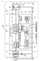
- FIG. 1 is a system configuration diagram illustrating a power conversion system according to a first embodiment.
- 1 is a circuit configuration diagram illustrating a power conversion device constituting a part of a power conversion system according to a first embodiment.
- 4A to 4C are diagrams illustrating common mode noise generated in the power conversion system according to the first embodiment.
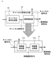
- 1 is a configuration diagram illustrating a noise filter and a power conversion system according to a first embodiment.
- 2 is a configuration diagram illustrating an example of a noise detection unit in the noise filter according to the first embodiment.
- FIG. 2 is a configuration diagram illustrating an example of a noise detection unit in the noise filter according to the first embodiment.
- FIG. 4 is a configuration diagram illustrating an example of a cancellation signal generating section in the noise filter according to the first embodiment.
- FIG. 2 is a configuration diagram illustrating an example of an abnormality detection unit in the noise filter according to the first embodiment.
- FIG. 2 is a configuration diagram illustrating an example of a feature detection unit in the noise filter according to the first embodiment.
- FIG. 4 is a configuration diagram illustrating an example of a feature comparison unit in the noise filter according to the first embodiment.
- FIG. 2 is a configuration diagram illustrating a cancellation signal injection section in the noise filter according to the first embodiment.
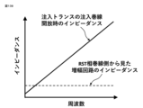
- FIG. 4 is a diagram illustrating the relationship between the impedance and frequency of an injection transformer during normal operation in the noise filter according to the first embodiment.
- FIG. 5A and 5B are diagrams for explaining behavior during a protective operation of an injection transformer in the noise filter according to the first embodiment.
- 5 is a diagram illustrating the relationship between impedance and frequency during a protective operation of an injection transformer in the noise filter according to the first embodiment.
- FIG. 2 is a configuration diagram illustrating an example of a protection circuit in the noise filter according to the first embodiment.
- FIG. FIG. 11 is a configuration diagram illustrating a noise filter according to a second embodiment.
- FIG. 11 is a configuration diagram illustrating another configuration example of the noise filter according to the second embodiment.
- FIG. 10A and 10B are diagrams illustrating an example of processing of an abnormality detection signal in a cancellation signal output unit in the noise filter according to the second embodiment.
- FIG. 11 is a configuration diagram illustrating a power conversion system according to a third embodiment.
- 13A and 13B are diagrams illustrating common mode noise generated in a power conversion system according to a third embodiment.
- FIG. 11 is a configuration diagram illustrating a noise filter according to a third embodiment.
- FIG. 21A is a diagram showing the control response when there is no filter portion
- FIG. 21B is a diagram showing the pass characteristics of the filter portion
- FIG. 21C is a diagram showing the control response when there is a filter portion.
- FIG. 21A is a diagram showing the control response when there is no filter portion
- FIG. 21B is a diagram showing the pass characteristics of the filter portion
- FIG. 21C is a diagram showing the control response when there is a filter portion.
- FIG. 21A is a diagram showing the control response when there is no filter
- FIG. 22A is a graph showing the gain characteristic
- FIG. 22B is a graph showing the phase characteristic.
- FIG. 23A is a graph showing the change in gain characteristics when a change occurs in the control characteristics due to the occurrence of an abnormality
- FIG. 23B is a graph showing the change in phase characteristics when a change occurs in the control characteristics due to the occurrence of an abnormality.
- 11 is a diagram illustrating an abnormal output waveform of a cancellation signal output section of a noise filter.
- 25A is a diagram showing the waveform of a common mode voltage under normal conditions
- FIG. 25B is a diagram showing the waveform of a common mode current under normal conditions
- FIG. 25A is a diagram showing the waveform of a common mode voltage under normal conditions
- FIG. 25B is a diagram showing the waveform of a common mode current under normal conditions
- FIG. 25C is a diagram showing the waveform of an output voltage of a cancellation signal in a noise filter under normal conditions
- FIG. 25D is a diagram showing the waveform of an output current of a cancellation signal in a noise filter under normal conditions.
- FIG. 26A is a diagram showing the waveform of a common mode voltage during an abnormality
- FIG. 26B is a diagram showing the waveform of a common mode current during an abnormality
- FIG. 26C is a diagram showing the waveform of an output voltage of a cancellation signal during an abnormality
- FIG. 26D is a diagram showing the waveform of an output current of a cancellation signal during an abnormality.
- FIG. 11 is a configuration diagram illustrating a noise filter and a power conversion system according to a fourth embodiment.
- FIG. 11 is a configuration diagram illustrating a noise filter and a power conversion system according to a fourth embodiment.
- FIG. 13 is a configuration diagram showing a management system according to a fifth embodiment.
- FIG. 13 is a configuration diagram illustrating a noise filter and a power conversion system according to a fifth embodiment.
- FIG. 13 is a configuration diagram illustrating a noise filter and a power conversion system according to a sixth embodiment.
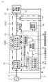
- Embodiment 1 A noise filter 100 and a power conversion system 500 according to the first embodiment will be described with reference to Fig. 1 to Fig. 11.
- Fig. 1 is a system configuration diagram showing the power conversion system 500 according to the first embodiment
- Fig. 2 is a circuit configuration diagram showing a power conversion device 80 constituting a part of the power conversion system 500 according to the first embodiment.
- the power conversion system 500 is arranged between an AC power source 1 and a load 90, and is composed of a power conversion device 80 that converts input power from the AC power source 1 into any DC power or AC power, the load 90 to which any DC power or AC power is supplied from the power conversion device 80, and a noise filter 100 provided on an electric circuit 11 that connects the power conversion device 80 and the load 90.
- the input power from the AC power source 1 is input to the power conversion device 80 via an electric circuit 2.
- the AC power source 1 is merely one example of a power source, and a DC power source may be used instead of the AC power source 1, and similarly, a DC power source may be used instead of the AC power source 1 in each of the embodiments described below.
- the power conversion device 80 converts the input power input from the AC power source 1 into the power required to drive the load 90 and outputs it.
- the noise filter 100 is disposed between the power conversion device 80 and the load 90, but it may also be provided in the electrical path 2 that connects the AC power source 1 and the power conversion device 80.
- the power conversion device 80 is, for example, a two-level three-phase inverter as shown in FIG. 2. That is, one upper and lower arm 82 is formed by two semiconductor switches 82a, 82b connected in series. Furthermore, one upper and lower arm 83 is formed by two semiconductor switches 83a, 83b connected in series. Furthermore, one upper and lower arm 84 is formed by two semiconductor switches 84a, 84b connected in series. A DC power supply 81 is connected to these three upper and lower arms 82, 83, 84.
- the DC power supply 81 is composed of a converter that converts the AC input power input from the AC power supply 1 into DC.
- the midpoints of the three upper and lower arms 82, 83, and 84 are connected to the inverter output terminal 85.
- These six semiconductor switches 82a, 82b, 83a, 83b, 84a, and 84b perform switching operations, outputting AC power to the inverter output terminal 85.
- the output potential of the inverter output terminal 85 becomes either the positive voltage or the negative voltage of the DC power supply 81. Therefore, the common mode voltage of the power conversion device 80 becomes a constant voltage that is not zero.
- FIG. 3 is a diagram explaining the common mode noise generated in the power conversion system 500 according to the first embodiment, and shows a common mode equivalent circuit.
- the AC power source 1 and the load 90 are connected on the ground side by a ground wire 3, separate from the above-mentioned electric circuit 11.
- the noise filter 100 is provided with a ground capacitor 15 (not shown) having one end connected to the ground line 3.
- Parasitic capacitance 86 and parasitic capacitance 91 exist between the power conversion device 80 and the ground line 3, and between the load 90 and the ground line 3, respectively.
- a common mode voltage Vcn generated in the power conversion device 80 is applied to the common mode loop via the parasitic capacitances 86, 91 and the ground line 3, so that a common mode current (common mode noise CN) flows in the direction shown by the arrow in FIG. 3.
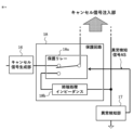
- FIG. 4 is a configuration diagram showing a noise filter 100 and a power conversion system 500 according to the first embodiment.
- the noise filter 100 is inserted between the power conversion device 80 and the load 90.
- the noise filter 100 is provided in an electrical path 11 that connects the power conversion device 80 and the load 90.
- the noise filter 100 comprises a noise detection unit 12 connected to the electrical circuit 2, a cancellation signal output unit 13 which generates and outputs a cancellation signal CS from common mode noise CN (not shown in FIG. 4) detected by the noise detection unit 12, a cancellation signal injection unit 14 which is provided on the electrical circuit 11 closer to the output end than the noise detection unit 12, i.e., on the load 90 side, and which injects the cancellation signal CS output from the cancellation signal output unit 13 into the electrical circuit 11, and a control power supply 19 which supplies power to the cancellation signal output unit 13 for generating and injecting the cancellation signal CS.
- the cancellation signal output unit 13 includes a cancellation signal generation unit 16 that amplifies the noise detection signal DS output from the noise detection unit 12, and an abnormality detection unit 17 that transmits the output from the cancellation signal generation unit 16 to the cancellation signal injection unit 14 as a cancellation signal CS and can output an abnormality detection signal AS based on the output voltage of the cancellation signal generation unit 16.
- the cancellation signal output unit 13 further includes a protection circuit 18, which is an example of a connection cut-off means that is inserted between the abnormality detection unit 17 and the cancellation signal injection unit 14 and can cut off the injection of the cancellation signal.
- the noise filter 100 according to the first embodiment includes a connection cut-off means that cuts off the connection between the cancellation signal output unit 13 and the cancellation signal injection unit 14, as a protection means for preventing the injection of an abnormal cancellation signal CS into the electrical circuit 11.
- the protection circuit 18 is used as one form of connection cut-off means.
- the abnormality detection unit 17 is composed of elements and circuits that have almost no effect on the output characteristics, so the output of the cancellation signal generation unit 16 is almost the same as the cancellation signal CS. Therefore, in the following explanation, unless otherwise specified, the output of the cancellation signal generation unit 16 will be referred to as the cancellation signal CS.
- a filter section capable of adjusting the characteristics of the cancellation signal CS may be provided between the noise detection section 12 and the cancellation signal generation section 16, or between the cancellation signal generation section 16 and the abnormality detection section 17.
- the cancellation signal generation section 16 will amplify the noise detection signal DS adjusted by the filter section to generate the cancellation signal CS. Even in this case, the characteristics of the cancellation signal CS will be adjusted by adjusting the noise detection signal DS.
- the above-mentioned filter section may be an input filter circuit that adjusts the attenuation characteristics of the noise filter 100, such as by reducing the gain of a specific band.
- an analog filter such as a high-pass filter, low-pass filter, or notch filter made up of resistors and capacitors may be used.
- a grounded capacitor 15 (not shown) is provided between the electric circuit 11 and the grounded wire 3.
- the noise detection unit 12, the cancellation signal injection unit 14, and the grounded capacitor 15 constitute the main circuit unit 101 of the noise filter 100.
- the control characteristics of the noise filter 100 are largely dependent on the main circuit unit 101.
- the inductance value of the main circuit unit 101 is the sum of the inductance value of the common mode transformer constituting the noise detection unit 12 and the inductance value of the common mode transformer constituting the cancellation signal injection unit 14.
- the capacitance value of the main circuit unit 101 is the capacitance value of the grounded capacitor 15.
- the power conversion system 500 includes a load 90, but the present invention is not limited to such a configuration.
- the main circuit unit 101 is constituted using a parasitic capacitance 91 that functions as the common mode impedance of the load 90.
- the control characteristics of the main circuit section 101 will be described in detail later.
- FIGS. 5A and 5B are configuration diagrams showing an example of the noise detection unit 12 in the noise filter 100 according to the first embodiment.
- the noise detection unit 12 is composed of a capacitor network.
- the multiple capacitors that make up the noise detection unit 12 are hereinafter referred to as the detection capacitor network 12n.
- the detection capacitor network 12n includes a detection capacitor 12a connected to the U-phase power line, a detection capacitor 12b connected to the V-phase power line, a detection capacitor 12c connected to the W-phase power line, and a detection capacitor 12e provided between the star connection point 12f connected to the other terminal of the detection capacitors 12a, 12b, and 12c that is not the power line and the ground wire 3 in the electric circuit 11 connecting the power conversion device 80 and the load 90.
- the detection capacitor network 12n operates as a noise detector that divides and detects the common mode voltage.
- the detection ratio of the common mode voltage in the detection capacitor network 12n is determined by the ratio between the parallel impedance of the detection capacitors 12a, 12b, and 12c and the impedance of the detection capacitor 12e. Therefore, in the noise detection unit 12, a noise detection signal DS is generated at both ends of the T-phase winding 12d due to the common mode noise CN applied to the detection capacitor network 12n.
- Both ends of the T-phase winding 12d are connected to the cancellation signal generating unit 16.
- the noise detection signal DS generated at both ends of the T-phase winding 12d is sent to the cancellation signal generating unit 16.
- the detection capacitor network 12n has an impedance that is sufficiently higher than the parasitic capacitance 86 of the inverter and the parasitic capacitance 91 of the load 90 in the common mode equivalent circuit shown in Figure 3, and therefore has a relatively high impedance to ground and does not adversely affect the leakage current of the power conversion device 80.
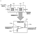
- FIG. 6 is a configuration diagram showing an example of the cancellation signal generating unit 16 in the noise filter 100 according to the first embodiment.
- the cancellation signal generating unit 16 includes an input resistor 16a, an operational amplifier 16b, and a feedback resistor 16c.
- the inverting input terminal of the operational amplifier 16b is connected to the input terminal side of the cancellation signal generating unit 16 (the left side in FIG. 6) via the input resistor 16a.
- the inverting input terminal of the operational amplifier 16b is connected to the output terminal of the operational amplifier 16b via the feedback resistor 16c.
- the non-inverting input terminal of the operational amplifier 16b is grounded.
- the cancellation signal generating unit 16 shown in FIG. 6 is an inverting amplifier circuit using the operational amplifier 16b, but it may also be a non-inverting amplifier circuit.
- the cancellation signal generating unit 16 amplifies the noise detection signal DS with an amplification factor given by the ratio between the resistance value of the input resistor 16a and the resistance value of the feedback resistor 16c to generate the cancellation signal CS, and outputs the cancellation signal CS.
- FIG. 7 is a configuration diagram showing an example of the anomaly detection unit 17 in the noise filter 100 according to the first embodiment.
- the anomaly detection unit 17 is composed of a feature detection unit 171 that outputs a feature signal CV for detecting an anomaly using the output voltage of the cancellation signal CS, and a feature comparison unit 172 that generates and outputs an anomaly detection signal AS by performing a predetermined calculation on the feature signal CV.
- the anomaly detection signal AS is output as an on-output
- the anomaly detection signal AS is output as an off-output.
- FIG. 8 is a configuration diagram showing an example of a feature detection unit 171 that is part of the anomaly detection unit 17 in the noise filter 100 according to the first embodiment.
- the feature detection unit 171 generates and outputs a feature signal CV based on the voltage value of the output voltage as the cancellation signal CS.
- the feature signal CV is a signal that represents a feature used for anomaly detection. Various values can be assumed to be used as the feature.
- An example of the feature detection unit 171 shown in FIG. 8 is a configuration of the feature detection unit 171 when the voltage average value of the output voltage as the cancellation signal CS is used as the feature.
- the feature detection unit 171 is configured by connecting a low-pass filter formed by a capacitor 171k and a resistor 171l to the output side of an absolute value detection circuit formed by operational amplifiers 171a and 171b, resistors 171c, 171d, 171e, 171h, 171i, 171j, and 171m, and diodes 171f and 171g.
- an input terminal (not shown) is connected to the output terminal (not shown) of the cancellation signal generation unit 16, and the output voltage as the cancellation signal CS output by the cancellation signal generation unit 16 is input as an input signal to the feature detection unit 171.
- the absolute value detection circuit outputs the absolute value of the voltage value of the output voltage as the cancellation signal CS.
- the output of the absolute value detection circuit is averaged by the low-pass filter, so that the above-mentioned low-pass filter outputs the average voltage value of the output voltage as the cancellation signal CS.
- the output of the feature detection unit 171 is the average voltage value of the output voltage as the cancellation signal CS.
- the output of the feature detection unit 171 is output to the feature comparison unit 172 as the feature signal CV. Note that the circuit of the feature detection unit 171 is not limited to the example shown in FIG. 8, and can be freely configured within the scope of the present application.
- FIG. 9 is a configuration diagram showing an example of the feature comparison unit 172, which is part of the anomaly detection unit 17 in the noise filter 100 according to the first embodiment.
- the feature comparison unit 172 generates an anomaly detection signal AS by performing a predetermined calculation on the feature signal CV output by the feature detection unit 171, and outputs the generated anomaly detection signal AS.
- FIG. 9 shows an example of the noise filter 100 according to the first embodiment, in which the feature comparison unit 172 is configured using a comparator circuit that compares the feature signal CV with a preset threshold voltage.
- the feature comparison unit 172 includes a comparator 172a, a DC voltage source 172b, and a pull-up resistor 172c.
- the inverting input terminal of the comparator 172a is connected to the input terminal side of the feature comparison unit 172 (left side of FIG. 9).
- the non-inverting input terminal of the comparator 172a is connected to the positive electrode of the DC voltage source 172b.
- the negative electrode of the DC voltage source 172b is grounded.
- the output terminal of the comparator 172a is connected to the output terminal side of the feature comparison unit 172.
- the pull-up resistor 172c is connected between the output terminal of the comparator 172a and the output terminal of the feature comparison unit 172.
- the voltage of the feature signal CV is compared with the voltage of the DC voltage source 172b, and an abnormality detection signal AS is output according to the result of the comparison. Specifically, for example, if the voltage of the feature signal CV is greater than the voltage of the DC voltage source 172b, an abnormality is detected and the abnormality detection signal AS is output as an ON signal. In this case, the voltage value of the DC voltage source 172b becomes the threshold voltage for determining whether or not an abnormality exists.
- the circuit that constitutes the feature comparison unit 172 is not limited to the example shown in FIG. 9, and can be freely configured within the scope of the present application.
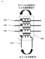
- FIG. 10 is a configuration diagram showing the cancellation signal injection unit 14 in the noise filter 100 according to the first embodiment.
- the cancellation signal injection unit 14 is composed of a common mode transformer.
- the common mode transformer constituting the cancellation signal injection unit 14 is hereinafter referred to as the injection transformer 14g.
- the injection transformer 14g includes an R-phase winding 14a wound around the R-phase power line, an S-phase winding 14b wound around the S-phase power line, a T-phase winding 14c wound around the T-phase power line, and an injection winding 14d.
- the R-phase winding 14a, the S-phase winding 14b, and the T-phase winding 14c are wound in the same phase.
- the injection transformer 14g configured as described above has a high inductance value only for the common mode and functions as a common mode choke coil.
- the cancellation signal injection unit 14 which is composed of the injection transformer 14g as described above, when the cancellation signal CS is input to both ends of the injection winding 14d, an induced voltage V that cancels the common mode noise CN is induced in the R-phase winding 14a, the S-phase winding 14b, and the T-phase winding 14c by the cancellation signal CS input to the injection winding 14d.
- the hardware configuration for realizing the control system according to the first embodiment may be configured with analog circuits as shown in Figures 8 and 9, but here we will explain an example that is different from analog circuits.
- FIG. 11 is an example of a hardware configuration diagram realizing the control system of the noise filter 100 according to the first embodiment.
- the "control system” here refers to the overall control of the noise filter 100, particularly including the control power supply 19.
- the control system of the noise filter 100 according to the first embodiment is mainly composed of a processor 71, a memory 72 as a main storage device, an auxiliary storage device 73, and an interface 74.
- the processor 71 is composed of, for example, a CPU (Central Processing Unit), an ASIC (Application Specific Integrated Circuit), a DSP (Digital Signal Processor), an FPGA (Field Programmable Gate Array), etc.
- a CPU Central Processing Unit
- ASIC Application Specific Integrated Circuit
- DSP Digital Signal Processor
- FPGA Field Programmable Gate Array
- Memory 72 is composed of a volatile storage device such as a random access memory, and auxiliary storage device 73 is composed of a non-volatile storage device such as a flash memory or a hard disk.
- a specific program executed by processor 71 is stored in auxiliary storage device 73.
- Processor 71 reads and executes this program as appropriate to perform various arithmetic processing. At this time, the above-mentioned specific program is temporarily saved from auxiliary storage device 73 to memory 72, and processor 71 reads the program from memory 72.
- the various types of arithmetic processing of the control system of the noise filter 100 and power conversion system 500 according to the first embodiment are realized by the processor 71 executing a predetermined program as described above.
- the results of the arithmetic processing by the processor 71 are temporarily stored in the memory 72, and are then stored in the auxiliary storage device 73 according to the purpose of the executed arithmetic processing.
- the control system may be realized by using either analog circuits or digital circuits.
- the following describes problems that may occur when an abnormality occurs in the control device of the noise filter 100, such as a temporary command value abnormality in the power conversion device 80 (the controlled device), an abnormality in the winding of the injection coil, or a component failure such as the transistor of the control circuit or the power supply capacitor.
- an abnormality occurs in the control device of the noise filter 100, such as a temporary command value abnormality in the power conversion device 80 (the controlled device), an abnormality in the winding of the injection coil, or a component failure such as the transistor of the control circuit or the power supply capacitor.
- the injection transformer 14g behaves as a common mode choke coil with the same number of turns in the main winding, and has a large inductance component.
- the resonant frequency between the injection transformer 14g and the load common mode capacitance fluctuates.
- the resonant frequency between the injection transformer 14g and the load common mode capacitance fluctuates, the resonant frequency of the fluctuated common mode path overlaps with the switching frequency of the power conversion device 80 and the band of its harmonic frequencies, which may instead cause a sudden increase in common mode noise CN.
- common mode noise CN it is necessary to increase the inductance component of the injection transformer 14g during protective operation by selecting a large number of turns for the injection transformer 14g so that the resonant frequency during protective operation is already lower than the switching frequency.
- increasing the number of turns for the injection transformer 14g undesirably increases the size of the noise filter 100.
- the common mode voltage share on the load side as viewed from the power conversion device 80, which is the noise source, is shared by the impedance ratio of the main circuit unit 101 shown in Fig. 4.
- the connection between the cancellation signal generation unit 16 and the cancellation signal injection unit 14 is cut off, the low output impedance of the cancellation signal generation unit 16 is no longer connected to the auxiliary winding connected to the control circuit side of the injection transformer 14g, and so the insertion impedance of the injection transformer 14g that constitutes the cancellation signal injection unit 14, which is part of the main circuit unit 101, increases significantly.
- the common mode voltage that the injection transformer 14g passively bears of the common mode noise CN shown in FIG. 3 increases significantly, which may cause magnetic saturation in the core. Magnetic saturation can cause problems such as heat generation, noise, and vibration, so it is necessary to avoid magnetic saturation, but an increase in the size of the core undesirably leads to an increase in the size of the noise filter 100.
- Figure 12A is a diagram explaining the behavior of the injection transformer 14g in the noise filter 100 according to embodiment 1 during normal operation
- Figure 12B is a diagram showing the relationship between the impedance and frequency during normal operation of the injection transformer 14g in the noise filter 100 according to embodiment 1.
- a cancellation signal generating unit 16 with low output impedance is connected to the injection winding 14d of the injection transformer 14g, and the cancellation signal injection unit 14 injects the cancellation signal CS into the electrical circuit 11.
- the insertion impedance in the common mode path of the injection transformer 14g is suppressed to a low value corresponding to the impedance of the amplifier circuit. Therefore, in the frequency band in which common mode noise CN occurs, there is no effect on the resonant frequency of the common mode path, and since the voltage sharing due to the common mode voltage is also low, magnetic saturation of the injection transformer 14g due to voltage sharing due to passive impedance does not occur.
- Figure 13A is a diagram explaining the behavior of the injection transformer 14g during protection operation in the noise filter 100 according to embodiment 1
- Figure 13B is a diagram showing the relationship between impedance and frequency during protection operation of the injection transformer 14g in the noise filter 100 according to embodiment 1.
- the injection winding 14d is open during protection operation. In other words, a high open impedance is connected to the injection winding 14d.
- the injection transformer 14g has an inductance component as a common mode choke coil corresponding to the core permeability, magnetic path length, cross-sectional area, and number of turns of the injection transformer 14g, and therefore behaves as an inductive impedance due to the inductance component, which greatly affects the resonance frequency of the common mode path. Furthermore, the voltage distribution resulting from the common mode voltage also increases significantly in the band where the common mode noise CN occurs, and as described above, there is a risk of magnetic saturation of the injection transformer 14g.
- FIG. 14 is a configuration diagram showing the protection circuit 18 of the noise filter 100 according to the first embodiment.
- the protection relay 18a constituting the protection circuit 18 can switch between two states by switching the relay contacts based on the abnormality detection signal AS: a noise cancellation operation state in which the cancellation signal injection unit 14 and the cancellation signal generation unit 16 are connected, and a noise cancellation stop state in which the cancellation signal injection unit 14 and the cancellation signal generation unit 16 are disconnected and the cancellation signal injection unit 14 is connected to the termination processing impedance 18b.
- the protective relay 18a is shown as a single C-contact relay, but it may be configured by combining different A-contact and B-contact relays, and may be configured as semiconductor relays as well as mechanical relays.
- the logic of the connected protective relay 18a may be such that a normally open contact is connected to the cancellation signal generating unit 16 and a normally closed contact is connected to the termination processing impedance 18b, or vice versa.
- the feature detection unit 171 outputs the effective voltage value of the output voltage of the cancellation signal CS as the feature signal CV. Furthermore, the DC voltage source 172b of the feature comparison unit 172 uses the output voltage value of the cancellation signal CS as the threshold voltage when determining whether or not there is an abnormality. In other words, the output voltage value of the DC voltage source 172b is the threshold voltage Vth of the effective voltage value. As a result, the feature comparison unit 172 compares the effective voltage value of the output voltage of the cancellation signal CS with the threshold voltage Vth of the effective voltage value.
- the output of the comparator 172a becomes high, and the feature comparison unit 172 outputs the abnormality detection signal AS as ON.
- the output of the comparator 172a becomes low, and the feature comparison unit 172 outputs the abnormality detection signal AS as OFF.
- the abnormality detection signal AS output from the feature comparison unit 172 is input to the protection circuit 18.
- the protection circuit 18 is typically configured with a control relay of a contact C. Based on the abnormality detection signal AS, the protection circuit 18 disconnects the control power supply 19 from the cancellation signal output unit 13, cuts off the connection between the cancellation signal output unit 13 and the cancellation signal injection unit 14, and connects the cancellation signal injection unit 14 to the termination impedance 18b.
- This operation of the cancellation signal output unit 13 cuts off the injection of the cancellation signal CS into the electric circuit 11, so that the injection of the cancellation signal CS having an abnormal output waveform into the electric circuit 11 can be prevented, and the resonance frequency fluctuation of the common mode path due to the insertion impedance fluctuation of the injection transformer 14g constituting the cancellation signal injection unit 14 and the occurrence of core magnetic saturation of the injection transformer 14g are suppressed.
- the abnormality detection unit 17 detects an abnormality and causes the protection circuit 18 to perform a cutoff operation
- the feature comparison unit 172 outputs an off-output of the abnormality detection signal AS
- the cutoff operation of the protection circuit 18 will be reset and the generation and injection of the cancellation signal CS will be restored.
- a delay circuit or counter circuit may be used to perform the recovery operation after a preset time has elapsed.
- an example of a circuit using operational amplifier 16b as the configuration of cancellation signal generation unit 16 is shown, but the configuration of cancellation signal generation unit 16 may be, for example, another inverting amplifier circuit or a non-inverting amplifier circuit.
- protection circuit 18 performs a cut-off operation in response to abnormality detection signal AS, but it is also possible to perform operations other than a simple cut-off operation by combining it with a logic circuit, such as latching the cut-off operation or being able to release the cut-off operation by combining it with a reset circuit.
- a circuit using an operational amplifier as the configuration of the feature detection unit 171
- it may be a circuit of another configuration that achieves the same purpose, for example.
- an example of using an effective voltage value as the detection quantity used by the feature detection unit 171 has been shown
- the feature detection unit 171 may be configured to detect a different value, such as an instantaneous value or an average value, as the feature.
- a circuit using a comparator 172a as the configuration of the feature comparison unit 172 it may be a different circuit that achieves the same purpose, for example.
- noise filter 100 in addition to the noise detection unit 12 and the cancellation signal injection unit 14, another common mode choke coil may be connected to the electrical path 11. Also, the noise detection unit 12 may be configured using a capacitor instead of a common mode transformer.
- the noise filter 100 is characterized in that it executes a process when an abnormality occurs in the cancellation signal CS, that is, an abnormality processing sequence.
- the abnormality processing sequence refers to the following sequence. (1) A sequence in which the protection circuit 18 is operated based on the abnormality detection signal AS, the injection of the cancellation signal CS into the electric circuit is cut off, and both ends of the cancellation signal injection unit 14 are connected to the termination impedance 18b. (2) A sequence in which the power conversion device 80 judges an abnormality based on the abnormality detection signal AS, and varies the switching frequency based on the resonance frequency predicted by the prediction calculation unit provided in the power conversion device 80.
- the abnormality processing sequence is, for example, any one of the above sequences (1) to (3). Details of the sequences (2) and (3) will be described in the sixth embodiment described later. It should be noted that the sequences listed above are merely examples of abnormality processing sequences, and needless to say, other processing that is effective in the event of an abnormality is also included.
- the noise filter 100 and power conversion system 500 according to the first embodiment operate stably even when an abnormality occurs in the cancellation signal, thereby achieving high reliability.
- an abnormality detection unit that detects abnormalities in the noise filter and power conversion device based on the output voltage or output current of the cancellation signal and outputs an abnormality detection signal
- a protection circuit that cuts off the connection between the cancellation signal injection unit and the cancellation signal output unit based on the abnormality detection signal and connects the cancellation signal injection unit to the termination processing impedance
- the abnormality is detected from a change in the output voltage or output current of the cancellation signal caused by the abnormal state, and the output of the cancellation signal from the cancellation signal output unit to the cancellation signal injection unit is suppressed, preventing the injection of the abnormal cancellation signal into the electrical circuit, and by connecting the termination impedance to the auxiliary winding of the injection transformer that constitutes the cancellation signal injection unit, an increase in common mode noise due to unintended resonance caused by fluctuations in the resonance frequency of the common mode path, or magnetic saturation due to an unintended increase in the insertion impedance of the injection transformer, can be prevented, thereby achieving a highly reliable noise
- FIG. 15 is a configuration diagram showing a noise filter 100a according to the second embodiment. Differences from the first embodiment will be mainly described.
- the cancellation signal injection unit 14 that injects the cancellation signal CS output from the cancellation signal output unit 13 into the electric circuit 11
- a plurality of cancellation signal injection units are provided and connected in series and parallel. This is because, when the noise filter 100a is provided between a large-capacity power conversion device and a load, in particular, it may be advantageous to configure the cancellation signal injection unit 14 in a divided manner due to problems with core implementation.
- FIG. 15 shows a configuration in which the cancellation signal injection section has three in series and two in parallel.
- the cancellation signal injection section 14 is composed of cancellation signal injection sections 14A1, 14A2, and 14A3 provided on one of the parallel electric paths 11A, and cancellation signal injection sections 14B1, 14B2, and 14B3 provided on the other parallel electric path 11B.
- the cancellation signal output unit 13 includes a control power supply 19 that supplies the cancellation signal output unit 13 with power for generating and injecting the cancellation signal CS, and a protection circuit 18 that is inserted between the control power supply 19 and the cancellation signal output unit 13 and that suppresses the injection of the cancellation signal CS into the electrical circuits 11A, 11B during protection operation and can be connected to the termination impedance 18b.
- the cancellation signal output unit 13 is provided for each unit of the number of cancellation signal injection units 14 in series.
- the noise filter 100a includes the same number of cancellation signal output units 13 as the number of cancellation signal injection units 14 in series.
- the noise filter 100a is configured with multiple cancellation signal injection sections, with the multiple cancellation signal injection sections arranged in series further arranged in parallel with respect to the electrical path, with the number of multiple cancellation signal injection sections being the same between the parallel sections.
- noise filter 100a configured as shown in FIG. 15, when a protection operation occurs in cancellation signal output unit 13, the protection operation is performed on cancellation signal injection units 14A1 and 14B1, and they are connected to the termination impedances 18b provided in each. In this case, the number of cancellation signal injection units 14 inserted between electrical paths 11A and 11B is maintained the same.
- FIG. 16 is a configuration diagram showing a noise filter 100b, which is another example of a noise filter according to embodiment 2. The differences from embodiment 1 and noise filter 100a according to embodiment 2 shown in FIG. 15 will be mainly described.
- the cancellation signal injection unit 14 that injects the cancellation signal CS output from the cancellation signal output unit 13 into the electrical circuit 11 is provided with a plurality of cancellation signal injection units that are connected in series and parallel.
- the cancellation signal injection unit 14 of the noise filter 100b has a configuration in which the number of series is N and the number of parallel connections is 2, similar to the configuration shown in FIG. 15.
- the noise filter 100b is composed of cancellation signal injection units 14A1, 14A2, 14A3, ... 14AN provided on one of the parallel electric paths 11A, and cancellation signal injection units 14B1, 14B2, 14B3, ... 14BN provided on the other parallel electric path 11B.
- the number of series, N may be determined appropriately based on the characteristics required for the noise filter 100b and the characteristics required for the power conversion system.
- the cancellation signal output unit 13 has a control power supply 19 that supplies the cancellation signal output unit 13 with power for generating and injecting the cancellation signal CS, and a protection circuit 18 that is inserted between the control power supply 19 and the cancellation signal output unit 13 and that suppresses the injection of the cancellation signal CS during protection operation and can be connected to a termination impedance 18b.
- N cancellation signal output units 13 are provided, which is the same number as the number of cancellation signal injection units 14 in series.
- the abnormality detection signal AS from the abnormality detection unit 17 in the cancellation signal output unit 13 connected to the cancellation signal injection unit 14A1 of one of the parallel electric circuits 11A is also input to the cancellation signal injection unit 14B1.
- the abnormality detection signal AS from the abnormality detection unit 17 in the cancellation signal output unit 13 connected to the cancellation signal injection unit 14B1 of the other parallel electric circuit 11B is also input to the cancellation signal injection unit 14A1.
- a similar configuration is arranged up to the combination of the cancellation signal injection unit 14AN and the cancellation signal injection unit 14BN.
- FIG. 17 shows an example of the configuration of the exchange of the abnormality detection signal AS between the cancellation signal output units 13 in the noise filter 100a shown in FIG. 15 and the noise filter 100b shown in FIG. 16.
- the abnormality detection signal AS output from the abnormality detection unit 17 is input to a wired-OR connected transistor circuit, for example, via a base resistor, and bundled into a single protection relay drive signal RY, which simultaneously switches the protection relays 18a of the two cancellation signal output units.
- the cancellation signal injection section is configured to be divided into a plurality of sections, so that an effect is achieved in that high reliability can be achieved even when the noise filter is provided between a large-capacity power conversion device and a load.
- Embodiment 3 A noise filter 100d and a power conversion system 500d according to the third embodiment will be described with reference to FIGS. 18 is an overall configuration diagram showing a power conversion system 500d according to embodiment 3.
- the power conversion system 500d includes a power conversion device 80 that is disposed between an AC power source 1 and a load 90 and converts input power from the AC power source 1 into any DC power or AC power, and a noise filter 100d inserted between the AC power source 1 and the power conversion device 80.
- the AC power source 1 and the noise filter 100d are connected by an electric path 2, and the noise filter 100d, the power conversion device 80, and the load 90 are connected by an electric path 11.
- the electric circuit 11 is connected to the electric circuit 2 of the AC power source 1, and the input power from the AC power source 1 is input to the power conversion device 80 via the electric circuit 2.
- the power conversion device 80 converts the power input from the AC power source 1 into power required to drive the load 90 and outputs it.
- the noise filter 100d is disposed between the AC power source 1 and the power conversion device 80, but it may be disposed between the power conversion device 80 and the load 90.
- FIG. 19 is a diagram for explaining common mode noise CN generated in a power conversion system 500d according to the third embodiment, showing a common mode equivalent circuit.
- the AC power source 1 and the load 90 are connected on the ground side by a ground wire 3 in addition to the above-mentioned electric circuit 11.
- the noise filter 100d is provided with a ground capacitor 15, one end of which is connected to the ground wire 3.
- a parasitic capacitance 86 and a parasitic capacitance 91 exist between the power conversion device 80 and the ground wire 3, and between the load 90 and the ground wire 3, respectively.
- a common mode voltage Vcn of the power conversion device 80 is applied to the common mode loop via the parasitic capacitances 86, 91, and the ground wire 3, and a common mode current (common mode noise CN) flows as shown by the arrow in FIG. 19.
- FIG. 20 is a configuration diagram showing a noise filter 100d according to the third embodiment.
- the noise filter 100d is inserted between the AC power supply 1 and the power conversion device 80.
- the noise filter 100d includes a noise detection unit 12 provided on the electric circuit 11 connected to the electric circuit 2, a cancellation signal output unit 13 that generates and outputs a cancellation signal CS from the common mode noise CN (not shown in FIG.
- a cancellation signal injection unit 14 that is provided on the electric circuit 11 closer to the output end than the noise detection unit 12, i.e., on the power conversion device 80 side, and injects the cancellation signal CS output from the cancellation signal output unit 13 into the electric circuit 11, a control power supply 19 that supplies power to the cancellation signal output unit 13 for generating and injecting the cancellation signal CS, and a protection circuit 18 that is inserted between the control power supply 19 and the cancellation signal output unit 13 and can cut off the supply of power from the control power supply 19.
- the noise filter 100d includes a protection circuit 18 that can cut off the connection between the cancellation signal output unit 13 and the cancellation signal injection unit 14 as a protection means for preventing an abnormal cancellation signal CS from being injected into the electrical circuit 11.
- the noise filter 100d according to the third embodiment differs from the noise filters according to the first and second embodiments in that it constitutes a feedback control system.
- a feedback control system has the advantage of being more robust against impedance errors in the controlled object than a feedforward system.
- a ground capacitor 15 connected between the electric circuit 11 and the ground wire 3 is provided, and the noise detection unit 12, the cancellation signal injection unit 14, and the ground capacitor 15 constitute a main circuit unit 101d in the power conversion system 500d.
- a filter unit 20 is provided between the noise detection unit 12 and the cancellation signal generation unit 16. The filter unit 20 adjusts the characteristics of the cancellation signal CS by adjusting the noise detection signal DS.
- the control characteristics of the noise filter 100d depend heavily on the main circuit section 101d.
- the inductance value of the main circuit section 101d is the sum of the inductance value of the common mode transformer that constitutes the noise detection section 12 and the inductance value of the injection transformer 14g that constitutes the cancellation signal injection section 14.
- the capacitance value of the main circuit section 101d is the capacitance value of the ground capacitor 15. The control characteristics of the main circuit section 101d will be described in detail later.
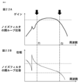
- Figures 21A, 21B, and 21C are diagrams showing the control response of the main circuit section 101d of the noise filter 100d according to embodiment 3.
- Figure 21A is a diagram showing the control response when there is no filter section 20
- Figure 21B is a diagram showing the pass characteristics of the filter section 20
- Figure 21C is a diagram showing the control response when there is a filter section 20.
- the horizontal axis is frequency and the vertical axis is gain.
- control response refers to the open-loop response in the path that starts from the output of the noise detection unit 12, passes through the cancellation signal output unit 13 and the cancellation signal injection unit 14, and returns to the noise detection unit 12.
- the control stability of the noise filter 100d depends on the values of the gain margin and phase margin of the open-loop response.
- the noise filter in the open loop response of the noise filter without the filter unit 20, a large resonance peak occurs at the resonance frequency f1 of the main circuit unit 101d, and the gain increases rapidly. Although not shown in FIG. 21A, phase rotation also occurs at the resonance frequency f1. In this way, without the filter unit 20, the noise filter has an unstable control response at the resonance frequency f1. If the common mode noise CN detected by the noise detection unit 12 contains a component of the resonance frequency f1, the cancellation signal CS may also become unstable.
- L1 is the inductance value of the main circuit unit 101d
- C1 is the capacitance value of the main circuit unit 101d.
- a filter section 20 having the filter pass characteristic shown in FIG. 21B is provided between the noise detection section 12 and the cancellation signal generation section 16.
- the filter section 20 is configured so that its reject frequency matches the resonance frequency f1 of the main circuit section 101d.
- Such a filter section 20 can be realized, for example, by a notch filter.
- the filter section 20 when the filter section 20 is provided between the noise detection section 12 and the cancellation signal generation section 16, even if the common mode noise CN detected by the noise detection section 12 contains a component of the resonance frequency f1, it is possible to generate a cancellation signal CS in which the resonance peak is attenuated. As a result, the noise filter 100d can exert a stable noise suppression effect.
- FIG. 22A and 22B are diagrams showing the control response of the noise filter 100d according to embodiment 3, with FIG. 22A showing the gain characteristic and FIG. 22B showing the phase characteristic.
- the control response characteristic (control characteristic) of the noise filter 100d the phase rotates due to the phase delay of the main circuit section 101d, the cancellation signal generating section 16, and the filter section 20.
- a notch filter and a low-pass filter are combined as the filter section 20 of the noise filter 100d to suppress the resonance peak at the resonance frequency f1 as described above, and the gain margin G2 at the phase inversion frequency f2 in the low frequency band and the gain margin G3 at the phase inversion frequency f3 in the high frequency band are set to values that ensure control stability.
- the gain margins G2 and G3 are indicated by upward arrows when they have positive values and by downward arrows when they have negative values.
- the value that ensures control stability is, for example, 6 dB.
- FIGS. 23A and 23B are diagrams showing the control response when a change in the control characteristics occurs due to the occurrence of an abnormality in the noise filter 100d according to embodiment 3, with FIG. 23A showing the change in gain characteristics and FIG. 23B showing the change in phase characteristics. Note that, in order to compare normal and abnormal conditions, the gain and phase characteristics in normal conditions are shown by solid lines, and the gain and phase characteristics in abnormal conditions are shown by dashed lines. Here, an example is shown as an "abnormality" in which the phase inversion frequency f3 in the high frequency band has changed to frequency f3*.
- a typical example of such an abnormality is when a component failure or other factor causes the low-pass filter to lose its function, resulting in a change in the characteristics of the filter section.
- the value of the gain margin G3 at the phase inversion frequency f3 in the high-frequency band fluctuates and may deviate from a value that ensures control stability.
- the gain margin at the high-frequency phase inversion frequency f3 fluctuates to a negative gain margin G3*. This indicates that the control response of the noise filter 100d is unstable.
- the cancellation signal CS output from the cancellation signal output unit 13 also becomes an unstable signal with an abnormal output waveform, and an abnormal and unstable cancellation signal CS is injected into the electrical circuit 11.
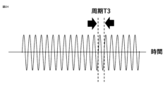
- FIG. 24 is a diagram showing an abnormal output waveform of the cancellation signal output unit 13 according to embodiment 3, showing an example of the waveform of the cancellation signal CS when an abnormality occurs.
- the horizontal axis represents time. Because the gain margin at the phase inversion frequency f3 is a negative value, the frequency component of the phase inversion frequency f3 continues to be amplified as shown in FIG. 24, causing oscillation. Note that the section between the arrow and the dashed line in FIG. 24 indicates the period T3 of the cancellation signal CS when an abnormality occurs. Period T3 is equal to the reciprocal of the phase inversion frequency f3.
- the noise source of the common mode noise CN also appears in the noise filter 100d.
- the load 90, the system, and the power conversion device 80 share the noise source voltage according to their respective impedance ratios.
- the cancellation signal injection unit 14 of the noise filter 100d according to the third embodiment is composed of an injection transformer 14g.
- the injection transformer 14g constituting the cancellation signal injection unit 14 is an inductive load with an inductive impedance for the cancellation signal output unit 13, and therefore has a high impedance in the high frequency band.
- the cancellation signal output unit 13 does not immediately produce phenomena that would affect the specifications of the circuit components, such as overvoltage or overcurrent. This means that since it is not possible to detect an abnormality in the noise filter, even if the noise filter is equipped with an overvoltage protection circuit or overcurrent protection circuit, the protection function will not stop the noise filter.
- the abnormality detection unit 17 detects an abnormality, and when an abnormality is detected, the protection circuit 18 is operated to stop the injection of the cancellation signal CS and connect the termination impedance 18b to the cancellation signal injection unit 14, thereby simultaneously solving the problem of constructing a feedback control system.
- the protection circuit 18 is operated to stop the injection of the cancellation signal CS and connect the termination impedance 18b to the cancellation signal injection unit 14, thereby simultaneously solving the problem of constructing a feedback control system.
- FIG. 25A shows the waveform of the common mode voltage under normal conditions
- FIG. 25B shows the waveform of the common mode current under normal conditions
- FIG. 25C shows the waveform of the output voltage of the cancellation signal CS under normal conditions for the noise filter 100d according to embodiment 3
- FIG. 25D shows the waveform of the output current of the cancellation signal CS under normal conditions.
- the horizontal axis represents time.
- the common mode voltage is the voltage of the common mode noise CN.
- the common mode current is the current that flows in the electrical circuit 11 due to the common mode voltage.
- the common mode current is the current that flows in the electrical circuit 11 when a common mode voltage is input to the common mode equivalent circuit shown in FIG. 19 and when it is assumed that the noise filter 100d is not present.
- the common mode voltage is generated by the switching operation of each semiconductor switch that constitutes the power conversion device 80 shown in FIG. 2, and has a rectangular waveform as shown in FIG. 25A.
- the common mode current has a spike-like waveform as shown in FIG. 25B, and causes noise problems at various points along the path.
- the noise detection unit 12 of the noise filter 100d detects the common mode current and transmits a noise detection signal DS to the cancellation signal output unit 13, which generates a cancellation signal CS from the noise detection signal DS.
- the cancellation signal CS is injected into the electrical circuit 11 via the cancellation signal injection unit 14.
- the output voltage of the cancellation signal CS under normal conditions has a spike-like waveform as shown in Figure 25C.
- the output current of the cancellation signal CS generated by the output voltage of the cancellation signal CS also has a spike-like waveform as shown in Figure 25D.
- the output current of the cancellation signal CS is a current that cancels out the common mode current, and so, like the common mode current, it has the characteristic of having a waveform whose effective value is extremely smaller than the peak value.
- the noise current flowing out from the power conversion device 80 which is the noise source of the common mode noise CN, passes through the cancellation signal injection unit 14, causing a disturbance component to be superimposed on the output current of the cancellation signal CS, and the disturbance component is also superimposed on the output voltage of the cancellation signal CS due to the product of the output impedance and current of the cancellation signal CS.
- the superimposition of disturbance components as described above is ignored in Figures 25C and 25D.
- FIG. 26A shows the waveform of the common mode voltage when an abnormality occurs
- FIG. 26B shows the waveform of the common mode current when an abnormality occurs
- FIG. 26C shows the waveform of the output voltage of the cancellation signal CS when an abnormality occurs in the noise filter 100d according to embodiment 3
- FIG. 26D shows the waveform of the output current of the cancellation signal CS when an abnormality occurs.
- the horizontal axis represents time.
- An abnormal output waveform does not have the characteristic of a normal waveform, that is, the characteristic of the effective value being extremely smaller than the peak value.
- the effective voltage value of the output voltage of the cancellation signal CS is 1/ ⁇ 2 times the voltage peak value, and there is no large difference between the peak value and the effective value.
- the effective current value of the output current of the cancellation signal CS is 1/ ⁇ 2 times the current peak value, and there is no significant difference between the peak value and the effective value. This is also true when the output voltage of the operational amplifier becomes saturated due to high-gain oscillation operation, causing the output voltage waveform of the cancellation signal CS to become rectangular.
- the effective voltage value of the output voltage of the cancellation signal CS and the effective current value of the output current are larger than in a normal state.
- the effective voltage value of the output voltage of the cancellation signal CS can be used as the criterion for determining an abnormality.
- an appropriate threshold voltage or threshold current can be set, and by comparing the actual effective voltage value with the threshold voltage or the actual effective current value with the threshold current, it can be determined whether the noise filter 100d is operating normally, i.e., whether the noise filter 100d is able to cancel the common mode current, or whether it has fallen into an abnormal operation for some reason.
- the threshold voltage of the effective voltage value for determining whether or not there is an abnormality is Vth
- the effective voltage value during abnormal operation is V2
- the presence or absence of an abnormality can be determined by selecting the threshold voltage Vth for the effective voltage value such that V1 ⁇ Vth ⁇ V2.
- the effective current value of the output current of the cancel signal CS is used to determine whether or not there is an abnormality.
- the noise filter according to the third embodiment has an effect of achieving high reliability even when the noise filter constitutes a feedback control system.
- the abnormality when an abnormality occurs in the noise filter that requires protection, the abnormality is detected from a change in the output voltage or output current of the cancellation signal CS due to the abnormality, and the output of the noise cancellation signal from the cancellation signal output unit to the cancellation signal injection unit is suppressed, preventing the injection of the abnormal cancellation signal into the electrical circuit.
- a termination impedance to the auxiliary winding of the injection transformer that constitutes the cancellation signal injection unit, an increase in common mode noise CN due to unintended resonance caused by fluctuations in the resonance frequency of the common mode path, or magnetic saturation due to an unintended increase in the insertion impedance of the injection transformer, is prevented, thereby achieving high reliability.
- an abnormality in the noise filter is detected based on the output voltage or output current of the cancellation signal CS, an abnormality in the noise filter in the high frequency band can be reliably detected even if the cancellation signal injection section of the cancellation signal CS is configured with an inductance load such as a common mode transformer (injection transformer).
- an inductance load such as a common mode transformer (injection transformer).
- the generation and injection of the cancellation signal CS is stopped by the protection circuit when an abnormality is detected, stable operation can be achieved while setting the gain margin and phase margin for suppressing controlled oscillation in the feedback control system lower than before.
- the ability to set the gain margin and phase margin lower than before means that the control gain of the noise filter can be improved, which has the effect of improving the amount of noise suppression.
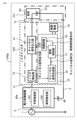
- FIG. 27 is a configuration diagram showing a noise filter 100e and a power conversion system 500e according to a fourth embodiment.
- the noise filters according to the first, second, and third embodiments all include a protection circuit 18 that performs an operation of disconnecting the cancellation signal injection unit 14 from the cancellation signal output unit and connecting the cancellation signal injection unit 14 to the termination processing impedance 18b in response to an abnormality detection signal AS.
- the noise filter 100e according to the fourth embodiment has a function of notifying the power conversion device 80, which is the noise source, of an abnormality in the noise filter 100e, instead of the above-mentioned protection circuit 18. Therefore, the protection circuit 18 is not an essential component of the noise filter 100e according to the fourth embodiment.
- an abnormal state signal output unit 21 is provided in the cancellation signal output unit 13, and the abnormality detection signal AS output by the abnormality detection unit 17 is input to the abnormal state signal output unit 21.
- the noise filter 100e according to the fourth embodiment has the abnormal state signal output unit 21 as a protection means for preventing an abnormal cancellation signal CS from being injected into the electric circuit 11.
- the abnormal state signal output unit 21 has an output circuit capable of outputting a signal to the power conversion device 80, and when the abnormality detection signal AS is input, it outputs an abnormal state signal AS2 to the power conversion device 80.
- the abnormal state signal AS2 is typically a differential signal that is resistant to external disturbances or a low-impedance current signal, and is generated based on the abnormality detection signal AS. Furthermore, the abnormal state signal AS2 is isolated from the control potential of the noise filter 100e as necessary.
- the power conversion device 80 which receives the abnormal state signal AS2, recognizes that the noise filter 100e is in an abnormal state.
- the power conversion device 80 which recognizes that the noise filter 100e is in an abnormal state, takes measures such as stopping operation depending on the nature of the abnormality, for example using a predictive calculation unit (not shown).
- a control circuit that stops the power conversion device 80 based on the abnormal state signal AS2 may be provided outside or inside the power conversion device 80. Such a control circuit receives the abnormal state signal AS2 and transmits a stop command to the power conversion device 80 as necessary.
- the noise filter according to the fourth embodiment is provided with the abnormal state signal output section, and therefore has the effect of providing a highly reliable noise filter.
- the noise filter according to the fourth embodiment differs from the first, second, and third embodiments in that it does not directly address problems such as fluctuations in the common mode resonant frequency due to fluctuations in the insertion impedance of the injection transformer 14g during protective operation and core magnetic saturation of the injection transformer 14g.
- the abnormal state signal is used to make the power conversion device, which is the noise source of the common mode noise CN, aware of an abnormality in the noise filter.
- the power conversion device takes measures such as stopping operation as necessary, so that stopping the noise source of the common mode noise CN has the effect of preventing an abnormal cancellation signal from being generated and injected into the electrical circuit, or an increase in the common mode noise CN due to an unintended common mode resonant frequency.
- the noise filter according to the fourth embodiment has the effect of realizing high reliability as a noise filter by indirectly preventing an abnormal cancellation signal CS from being injected into the electrical circuit or an unintended increase in common mode noise CN by making the power conversion device 80, which is the noise source, aware of an abnormality in the noise filter.
- the noise filter 100e according to the fourth embodiment may be combined with the protection circuit 18 of the noise filter according to the first, second, and third embodiments. Since the noise filter 100e according to the fourth embodiment outputs the abnormal state signal AS2 to the noise source of the common mode noise CN, if there is another controlled device that is a noise source of the common mode noise CN, the noise filter 100e may be configured to output the abnormal state signal AS2 to the other controlled device as well.
- Embodiment 5. 28 is a configuration diagram showing a management system 1000 according to embodiment 5.
- the management system 1000 includes a power conversion system 500f and a management device 200.
- the power conversion system 500f is composed of a power conversion device 80 that is disposed between an AC power source 1 and a load 90 and converts input power from the AC power source 1 into any DC power or AC power, a load 90 to which any DC power or AC power is supplied from the power conversion device 80, and a noise filter 100f having a communication function that is provided on an electric circuit 11 that connects the power conversion device 80 and the load 90.
- the noise filter 100f may also be provided on an electric circuit 2 that connects the AC power source 1 and the power conversion device 80.
- a DC power source may be used instead of the AC power source 1.
- FIG. 29 is a configuration diagram showing a noise filter 100f with a communication function, which is applied to a power conversion system 500f according to embodiment 5.
- the power conversion system 500f according to embodiment 5 differs in configuration from the noise filter 100 according to embodiment 1 in that the noise filter 100f includes a communication unit 24 connected to the cancellation signal output unit 13.
- the communication unit 24 which is part of the configuration of the noise filter 100f, converts various signals generated inside the cancellation signal output unit 13, such as the cancellation signal CS and the abnormality detection signal AS, into digital data and transmits the data to the outside of the power conversion system 500f.
- the Internet may be used for transmission.
- the management device 200 constituting the management system 1000 includes a receiving unit 201, a database 202, a data analysis unit 203, and a transmitting unit 204, as shown in FIG. 28.
- the receiving unit 201 receives data transmitted to the outside of the power conversion system 500f via the communication unit 24 of the noise filter 100f, and stores the data in the database 202.
- the receiving unit 201 can also simultaneously receive data transmitted from each of the power conversion systems 500f owned by multiple clients.
- the database 202 sequentially stores the data transmitted from the power conversion system 500f. Note that data transmitted separately from multiple power conversion systems 500f for different clients may be stored separately in areas in the database 202 designated for each client.
- the data analysis unit 203 performs various analyses of the tendency, frequency, and cause of abnormalities that occur in the power conversion system 500f based on the data stored in the database 202.
- One example of the analysis is to diagnose each part of the power conversion device 80, such as determining whether it is better to replace it since the power conversion device 80 has a high failure frequency.
- the transmission unit 204 transmits the analysis results of the data analysis unit 203 to an external device outside the management system 1000, for example, via the Internet.
- Examples of the transmission destination include the management system of a client that operates the power conversion system 500f.
- the abnormality detection unit 17 transmits an abnormality detection signal AS, and the protection circuit 18 operates to perform a protective operation by cutting off the connection between the cancellation signal generation unit 16 and the cancellation signal injection unit 14, thereby achieving high reliability in the power conversion system 500f.
- the management system 1000 according to the fifth embodiment is applied, the data transmitted from the power conversion system 500f to the management device 200 is analyzed by the data analysis unit 203, and it becomes possible to, for example, determine the cause of the abnormality and propose a method of dealing with the abnormality to resolve it, thereby eliminating the cause of the abnormality at an early stage, and thus the reliability of the power conversion system 500f is further improved.
- the management system 1000 it becomes possible to grasp the operating status of the power conversion system 500f remotely, which facilitates management and maintenance of the power conversion system 500f. Furthermore, for the client who operates the power conversion system 500f, the analysis results and countermeasures for abnormalities by the management device 200 can be easily obtained, for example, via the Internet, so that maintenance and inspection of the power conversion system 500f can be performed at the appropriate time, or the number of maintenance and inspections can be reduced, thereby simultaneously realizing labor savings.
- the management system 1000 has the management device 200 that performs data analysis using data transmitted from the power conversion system 500f. This makes it possible to quickly address the cause of an abnormality, thereby achieving the effect of further improving the reliability of the power conversion system 500. Furthermore, this also has the effect of improving the maintainability, such as the management and maintenance of the power conversion system.
- FIG. 30 is a configuration diagram showing the power conversion system 500g according to the sixth embodiment.
- the power conversion system 500g according to the sixth embodiment differs from the power conversion system 500 according to the first embodiment in that a power conversion device 80a includes a prediction calculation unit 181 and an abnormality estimation unit 182.
- the configuration of the noise filter 100 is the same as that of the first embodiment.
- the prediction calculation unit 181 of the power conversion device 80a recognizes that the noise filter 100 is in an abnormal state and outputs a resonant frequency prediction value based on the abnormality detection signal AS.
- the prediction calculation unit 181 can also take measures to vary the switching frequency based on the resonant frequency prediction value.
- the abnormality estimation unit 182 of the power conversion device 80a outputs an abnormality continuation judgment value if the abnormality detection signal AS continues for a preset period or longer. Furthermore, it is also possible to stop the operation of the power conversion device 80a based on the abnormality continuation judgment value.
- a prediction calculation unit and an abnormality estimation unit are provided inside the power conversion device, so that it is possible to respond to abnormal conditions on the power conversion device side as well, thereby achieving the effect of providing a highly reliable power conversion system.
Landscapes
- Engineering & Computer Science (AREA)
- Power Engineering (AREA)
- Inverter Devices (AREA)
Abstract
A noise filter (100) according to the present disclosure is provided to either a cable run (2) connecting an AC or DC power source (1) and a power conversion device (80) that converts power outputted from the power source (1) into AC or DC power or a cable run (11) connecting the power conversion device (80) and a load. The noise filter comprises: a noise detection unit (12) that detects common-mode noise generated during the operation of the power conversion device (80); a cancellation signal generation unit (16) that generates a cancellation signal which cancels the common-mode noise; a cancellation signal injection unit (14) that injects the cancellation signal into the cable run (2, 11); and an abnormality detection unit (17) that outputs an abnormality detection signal when the cancellation signal is detected to be abnormal. The noise filter (100) executes an abnormality processing sequence on the basis of the abnormality detection signal.
Description
本開示は、ノイズフィルタ、電力変換システム及び管理システムに関する。
This disclosure relates to noise filters, power conversion systems, and management systems.
電源からの入力電力を任意の直流電力または交流電力に変換して負荷に供給する電力変換装置が知られている。このような電力変換装置は、ブリッジ接続された複数のスイッチング素子を開閉させて電力変換を行うが、スイッチング素子の動作に伴い高周波ノイズが発生する。この高周波ノイズは寄生容量などを介して接地電位を経由し、電源または負荷に流れるコモンモードノイズの原因となる。そこで、このようなコモンモードノイズを抑制するために、電源と電力変換装置との間の電路、または電力変換装置と負荷との間の電路にノイズフィルタを設置する構成が知られている。
Power conversion devices are known that convert input power from a power source into any DC or AC power and supply it to a load. Such power conversion devices perform power conversion by opening and closing multiple bridge-connected switching elements, but high-frequency noise is generated as the switching elements operate. This high-frequency noise passes through parasitic capacitance and other factors to the ground potential, causing common-mode noise to flow to the power source or load. Therefore, in order to suppress such common-mode noise, a configuration is known in which a noise filter is installed in the electrical path between the power source and the power conversion device, or in the electrical path between the power conversion device and the load.
ノイズフィルタの一つにアクティブノイズフィルタがある。例えば、特許文献1に記載のアクティブノイズフィルタは、交流電源と整流器の間の電路に接続された接地コンデンサを介してコモンモード電圧を検出し、相殺用電圧源によって検出したコモンモード電圧と同じ大きさで逆極性の相殺用電圧を発生させ、電路における交流電源と接地コンデンサの接続点との間に相殺用電圧を重畳させる。このように、特許文献1に記載のアクティブノイズフィルタは、コモンモードノイズであるコモンモード電圧を相殺する相殺用電圧をノイズキャンセル信号(以下、キャンセル信号と呼ぶ)として電路に注入するものである。
One type of noise filter is the active noise filter. For example, the active noise filter described in Patent Document 1 detects the common mode voltage via a grounded capacitor connected to the electrical path between the AC power supply and the rectifier, generates a cancellation voltage of the same magnitude and opposite polarity as the common mode voltage detected by a cancellation voltage source, and superimposes the cancellation voltage between the connection point of the AC power supply and the grounded capacitor in the electrical path. In this way, the active noise filter described in Patent Document 1 injects a cancellation voltage that cancels out the common mode voltage, which is common mode noise, into the electrical path as a noise cancellation signal (hereinafter referred to as a cancellation signal).
アクティブノイズフィルタの動作中に、環境要因または経時要因などにより、アクティブノイズフィルタの制御特性が変化する場合がある。特許文献1に記載のアクティブノイズフィルタでは、設計当初には想定されていなかったような制御特性の変化が生じた場合、制御余裕(ゲイン余裕および位相余裕)の喪失などにより、電路に注入されるキャンセル信号が発振する、あるいはノイズキャンセルにおける補償量が過大になるといった異常なキャンセル信号が生成されるおそれがある。
During the operation of an active noise filter, the control characteristics of the active noise filter may change due to environmental factors or factors that have passed over time. In the active noise filter described in Patent Document 1, if a change in the control characteristics occurs that was not anticipated at the time of the initial design, there is a risk that an abnormal cancellation signal will be generated, such as the cancellation signal injected into the electrical circuit oscillating due to a loss of control margin (gain margin and phase margin) or the amount of compensation in noise cancellation becoming excessive.
異常なキャンセル信号が電路に注入された場合、コモンモードノイズをキャンセル、つまり相殺できないばかりでなく、キャンセル信号自体が問題を引き起こす可能性もある。
If an abnormal cancellation signal is injected into an electrical circuit, not only will it not be possible to cancel, or offset, the common mode noise, but the cancellation signal itself may cause problems.
本開示は、上述のような課題を解決するためになされたものであり、高い信頼性を実現することができるノイズフィルタ、電力変換システム及び管理システムを提供することを目的とする。
This disclosure has been made to solve the problems described above, and aims to provide a noise filter, power conversion system, and management system that can achieve high reliability.
本願に開示されるノイズフィルタは、
交流または直流電源と前記交流または直流電源から出力された電力を交流または直流電力に変換する電力変換装置とを接続する電路、あるいは、前記電力変換装置と負荷とを接続する電路のいずれか一方の電路に設けられたノイズフィルタであって、
前記電力変換装置の動作時に発生するコモンモードノイズを検出するノイズ検出部と、
前記コモンモードノイズを相殺するキャンセル信号を生成するキャンセル信号生成部と、
前記キャンセル信号を前記電路に注入するキャンセル信号注入部と、
前記キャンセル信号が異常であると検知した場合に異常検知信号を出力する異常検知部と、を備え、
前記異常検知信号に基づき異常処理シーケンスを実行することを特徴とする。 The noise filter disclosed in the present application comprises:
A noise filter provided in either an electric path connecting an AC or DC power source and a power conversion device that converts power output from the AC or DC power source into AC or DC power, or an electric path connecting the power conversion device and a load,
A noise detection unit that detects common mode noise generated during operation of the power conversion device;
a cancellation signal generating unit that generates a cancellation signal that cancels the common mode noise;
a cancellation signal injection unit that injects the cancellation signal into the electrical path;
an abnormality detection unit that outputs an abnormality detection signal when detecting that the cancellation signal is abnormal;
The abnormality processing sequence is executed based on the abnormality detection signal.
本願に開示される電力変換システムは、
交流または直流電源から出力された電力を交流または直流電力に変換する電力変換装置と、
上述のノイズフィルタと、を備える。 The power conversion system disclosed in the present application comprises:
a power conversion device that converts power output from an AC or DC power source into AC or DC power;
The noise filter described above.
交流または直流電源から出力された電力を交流または直流電力に変換する電力変換装置と、
上述のノイズフィルタと、を備える。 The power conversion system disclosed in the present application comprises:
a power conversion device that converts power output from an AC or DC power source into AC or DC power;
The noise filter described above.
本願に開示される管理システムは、
交流または直流電源から出力された電力を交流または直流電力に変換する電力変換装置と、
上述のノイズフィルタを構成するキャンセル信号出力部に接続され、データを外部に送信する通信部をさらに備える前記ノイズフィルタと、
前記通信部から送信された前記データを格納するデータベース及び前記データを分析するデータ分析部を有する管理装置と、を備える。 The management system disclosed in the present application comprises:
a power conversion device that converts power output from an AC or DC power source into AC or DC power;
The noise filter further includes a communication unit connected to a cancellation signal output unit constituting the noise filter and configured to transmit data to an outside.
and a management device having a database for storing the data transmitted from the communication unit and a data analysis unit for analyzing the data.
本願に開示されるノイズフィルタ及び電力変換システムによれば、キャンセル信号に異常が発生した場合においても安定に動作するため、高い信頼性を実現することが可能となるという効果を奏する。
The noise filter and power conversion system disclosed in this application have the effect of providing high reliability by operating stably even when an abnormality occurs in the cancellation signal.
本願に開示される管理システムによれば、電力変換システムから送信されるデータを用いてデータ分析を行う管理装置を有するので、異常となる原因に迅速に対処することが可能となるため、電力変換システムの信頼性が一層向上するという効果を奏し、さらに、電力変換システムの管理、保守といったメンテナンス性が向上するという効果を奏する。
The management system disclosed in this application has a management device that performs data analysis using data transmitted from the power conversion system, making it possible to quickly address the cause of an abnormality, which has the effect of further improving the reliability of the power conversion system and also has the effect of improving the maintainability of the power conversion system, such as management and maintenance.
以下、本願の各実施の形態におけるノイズフィルタについて、図面を参照して詳細に説明する。なお、各図において同一符号は同一もしくは相当部分を示している。
The noise filters in each embodiment of the present application will be described in detail below with reference to the drawings. Note that the same reference numerals in each drawing indicate the same or corresponding parts.
実施の形態1.
実施の形態1に係るノイズフィルタ100及び電力変換システム500を図1から図11に基づいて説明する。図1は、実施の形態1に係る電力変換システム500を示すシステム構成図であり、図2は、実施の形態1に係る電力変換システム500の一部を構成する電力変換装置80を示す回路構成図である。Embodiment 1.
Anoise filter 100 and a power conversion system 500 according to the first embodiment will be described with reference to Fig. 1 to Fig. 11. Fig. 1 is a system configuration diagram showing the power conversion system 500 according to the first embodiment, and Fig. 2 is a circuit configuration diagram showing a power conversion device 80 constituting a part of the power conversion system 500 according to the first embodiment.
実施の形態1に係るノイズフィルタ100及び電力変換システム500を図1から図11に基づいて説明する。図1は、実施の形態1に係る電力変換システム500を示すシステム構成図であり、図2は、実施の形態1に係る電力変換システム500の一部を構成する電力変換装置80を示す回路構成図である。
A
電力変換システム500は、交流電源1と負荷90との間に配置され、交流電源1からの入力電力を任意の直流電力または交流電力に変換する電力変換装置80と、電力変換装置80から任意の直流電力または交流電力を供給される負荷90と、電力変換装置80と負荷90とを接続する電路11に設けられたノイズフィルタ100と、で構成される。交流電源1からの入力電力は、電路2を介して電力変換装置80に入力される。なお、交流電源1は電源の一例に過ぎず、交流電源1の代りに直流電源であってもよく、後述する各実施の形態においても同様に、交流電源1の代りに直流電源を適用してもよい。
The power conversion system 500 is arranged between an AC power source 1 and a load 90, and is composed of a power conversion device 80 that converts input power from the AC power source 1 into any DC power or AC power, the load 90 to which any DC power or AC power is supplied from the power conversion device 80, and a noise filter 100 provided on an electric circuit 11 that connects the power conversion device 80 and the load 90. The input power from the AC power source 1 is input to the power conversion device 80 via an electric circuit 2. Note that the AC power source 1 is merely one example of a power source, and a DC power source may be used instead of the AC power source 1, and similarly, a DC power source may be used instead of the AC power source 1 in each of the embodiments described below.
電力変換装置80は、交流電源1から入力される入力電力を負荷90の駆動に必要な電力に変換して出力する。なお、実施の形態1において、ノイズフィルタ100は電力変換装置80と負荷90との間に配置されているが、交流電源1と電力変換装置80とを接続する電路2に設けられてもよい。
The power conversion device 80 converts the input power input from the AC power source 1 into the power required to drive the load 90 and outputs it. Note that in the first embodiment, the noise filter 100 is disposed between the power conversion device 80 and the load 90, but it may also be provided in the electrical path 2 that connects the AC power source 1 and the power conversion device 80.
電力変換装置80は、例えば、図2に示すような2レベル三相インバータである。すなわち、直列に接続された2つの半導体スイッチ82a、82bによって、1つの上下アーム82が構成されている。また、直列に接続された2つの半導体スイッチ83a、83bによって1つの上下アーム83が構成されている。さらに、直列に接続された2つの半導体スイッチ84a、84bによって1つの上下アーム84が構成されている。この3つの上下アーム82、83、84には直流電源81が接続されている。
The power conversion device 80 is, for example, a two-level three-phase inverter as shown in FIG. 2. That is, one upper and lower arm 82 is formed by two semiconductor switches 82a, 82b connected in series. Furthermore, one upper and lower arm 83 is formed by two semiconductor switches 83a, 83b connected in series. Furthermore, one upper and lower arm 84 is formed by two semiconductor switches 84a, 84b connected in series. A DC power supply 81 is connected to these three upper and lower arms 82, 83, 84.
直流電源81は、交流電源1から入力される交流の入力電力を直流に変換するコンバータなどで構成される。3つの上下アーム82、83、84の中点は、インバータ出力端子85に接続されている。これらの6つの半導体スイッチ82a、82b、83a、83b、84a、84bがスイッチング動作を行うことで、インバータ出力端子85に交流電力が出力される。このとき、インバータ出力端子85の出力電位は、直流電源81の正電圧および負電圧のいずれか一方の電位となる。したがって、電力変換装置80のコモンモード電圧は、ゼロではない一定の電圧となる。
The DC power supply 81 is composed of a converter that converts the AC input power input from the AC power supply 1 into DC. The midpoints of the three upper and lower arms 82, 83, and 84 are connected to the inverter output terminal 85. These six semiconductor switches 82a, 82b, 83a, 83b, 84a, and 84b perform switching operations, outputting AC power to the inverter output terminal 85. At this time, the output potential of the inverter output terminal 85 becomes either the positive voltage or the negative voltage of the DC power supply 81. Therefore, the common mode voltage of the power conversion device 80 becomes a constant voltage that is not zero.
図3は、実施の形態1に係る電力変換システム500に発生するコモンモードノイズを説明する図であり、コモンモード等価回路を示す。電力変換システム500において、交流電源1と負荷90とは、上述した電路11とは別に、接地線3によってグランド側で接続されている。
FIG. 3 is a diagram explaining the common mode noise generated in the power conversion system 500 according to the first embodiment, and shows a common mode equivalent circuit. In the power conversion system 500, the AC power source 1 and the load 90 are connected on the ground side by a ground wire 3, separate from the above-mentioned electric circuit 11.
ノイズフィルタ100には、一方の端部が接地線3に接続される接地コンデンサ15(図示せず)が設けられている。また、電力変換装置80と接地線3との間、および負荷90と接地線3との間には、寄生容量86および寄生容量91がそれぞれ存在する。電力変換システム500では、寄生容量86、91および接地線3を介するコモンモードループに対して、電力変換装置80において発生するコモンモード電圧Vcnが印加されるため、図3において矢印で示す方向に、コモンモード電流(コモンモードノイズCN)が流れる。
The noise filter 100 is provided with a ground capacitor 15 (not shown) having one end connected to the ground line 3. Parasitic capacitance 86 and parasitic capacitance 91 exist between the power conversion device 80 and the ground line 3, and between the load 90 and the ground line 3, respectively. In the power conversion system 500, a common mode voltage Vcn generated in the power conversion device 80 is applied to the common mode loop via the parasitic capacitances 86, 91 and the ground line 3, so that a common mode current (common mode noise CN) flows in the direction shown by the arrow in FIG. 3.
図4は、実施の形態1に係るノイズフィルタ100および電力変換システム500を表す構成図である。ノイズフィルタ100は、電力変換装置80と負荷90の間に挿入されている。すなわち、電力変換装置80と負荷90とを接続する電路11に設けられている。
FIG. 4 is a configuration diagram showing a noise filter 100 and a power conversion system 500 according to the first embodiment. The noise filter 100 is inserted between the power conversion device 80 and the load 90. In other words, the noise filter 100 is provided in an electrical path 11 that connects the power conversion device 80 and the load 90.
ノイズフィルタ100は、電路2に接続するノイズ検出部12と、ノイズ検出部12によって検出されたコモンモードノイズCN(図4では図示せず)からキャンセル信号CSを生成して出力するキャンセル信号出力部13と、ノイズ検出部12よりも出力端側、すなわち負荷90側の電路11に設けられ、キャンセル信号出力部13から出力されたキャンセル信号CSを電路11に注入するキャンセル信号注入部14と、キャンセル信号CSを生成および注入するための電力をキャンセル信号出力部13に供給する制御電源19と、を備える。
The noise filter 100 comprises a noise detection unit 12 connected to the electrical circuit 2, a cancellation signal output unit 13 which generates and outputs a cancellation signal CS from common mode noise CN (not shown in FIG. 4) detected by the noise detection unit 12, a cancellation signal injection unit 14 which is provided on the electrical circuit 11 closer to the output end than the noise detection unit 12, i.e., on the load 90 side, and which injects the cancellation signal CS output from the cancellation signal output unit 13 into the electrical circuit 11, and a control power supply 19 which supplies power to the cancellation signal output unit 13 for generating and injecting the cancellation signal CS.
キャンセル信号出力部13は、ノイズ検出部12から出力されるノイズ検出信号DSを増幅するキャンセル信号生成部16と、キャンセル信号生成部16からの出力をキャンセル信号CSとしてキャンセル信号注入部14に送信するとともにキャンセル信号生成部16の出力電圧に基づいて異常検知信号ASを出力することができる異常検知部17と、を備える。
The cancellation signal output unit 13 includes a cancellation signal generation unit 16 that amplifies the noise detection signal DS output from the noise detection unit 12, and an abnormality detection unit 17 that transmits the output from the cancellation signal generation unit 16 to the cancellation signal injection unit 14 as a cancellation signal CS and can output an abnormality detection signal AS based on the output voltage of the cancellation signal generation unit 16.
キャンセル信号出力部13は、さらに、異常検知部17とキャンセル信号注入部14との間に挿入され、キャンセル信号の注入の遮断することができる接続遮断手段の一例である保護回路18を備える。すなわち、実施の形態1に係るノイズフィルタ100は、異常なキャンセル信号CSが電路11に注入されることを抑制するための保護手段として、キャンセル信号出力部13とキャンセル信号注入部14との間の接続を遮断する接続遮断手段を備える。実施の形態1では、接続遮断手段の一形態として保護回路18を適用している。
The cancellation signal output unit 13 further includes a protection circuit 18, which is an example of a connection cut-off means that is inserted between the abnormality detection unit 17 and the cancellation signal injection unit 14 and can cut off the injection of the cancellation signal. That is, the noise filter 100 according to the first embodiment includes a connection cut-off means that cuts off the connection between the cancellation signal output unit 13 and the cancellation signal injection unit 14, as a protection means for preventing the injection of an abnormal cancellation signal CS into the electrical circuit 11. In the first embodiment, the protection circuit 18 is used as one form of connection cut-off means.
なお、実施の形態1において、異常検知部17は出力特性にほとんど影響を与えない素子および回路で構成されているので、キャンセル信号生成部16の出力はキャンセル信号CSとほぼ同じになる。したがって、以下の説明では特に断りが無い限り、キャンセル信号生成部16の出力をキャンセル信号CSと呼ぶ。
In addition, in the first embodiment, the abnormality detection unit 17 is composed of elements and circuits that have almost no effect on the output characteristics, so the output of the cancellation signal generation unit 16 is almost the same as the cancellation signal CS. Therefore, in the following explanation, unless otherwise specified, the output of the cancellation signal generation unit 16 will be referred to as the cancellation signal CS.
なお、ノイズ検出部12とキャンセル信号生成部16の間、またはキャンセル信号生成部16と異常検知部17との間に、キャンセル信号CSの特性を調整することができるフィルタ部(図示せず)を設けてもよい。ノイズ検出部12とキャンセル信号生成部16の間にフィルタ部が設けられている場合、キャンセル信号生成部16は、フィルタ部によって調整されたノイズ検出信号DSを増幅してキャンセル信号CSを生成することとなる。この場合でも、ノイズ検出信号DSの調整を介してキャンセル信号CSの特性が調整されることとなる。
A filter section (not shown) capable of adjusting the characteristics of the cancellation signal CS may be provided between the noise detection section 12 and the cancellation signal generation section 16, or between the cancellation signal generation section 16 and the abnormality detection section 17. When a filter section is provided between the noise detection section 12 and the cancellation signal generation section 16, the cancellation signal generation section 16 will amplify the noise detection signal DS adjusted by the filter section to generate the cancellation signal CS. Even in this case, the characteristics of the cancellation signal CS will be adjusted by adjusting the noise detection signal DS.
上述のフィルタ部としては、特定帯域のゲインを減少させるなど、ノイズフィルタ100の減衰特性を調整する入力フィルタ回路などが挙げられる。具体的には、例えば、抵抗およびコンデンサで構成されるハイパスフィルタ、ローパスフィルタ、またはノッチフィルタなどのアナログフィルタを適用することが挙げられる。
The above-mentioned filter section may be an input filter circuit that adjusts the attenuation characteristics of the noise filter 100, such as by reducing the gain of a specific band. Specifically, for example, an analog filter such as a high-pass filter, low-pass filter, or notch filter made up of resistors and capacitors may be used.
ノイズフィルタ100では、電路11と接地線3との間に接続された接地コンデンサ15(図示せず)が設けられている。ノイズ検出部12、キャンセル信号注入部14、および接地コンデンサ15は、ノイズフィルタ100の主回路部101を構成する。ノイズフィルタ100の制御特性は、主回路部101に大きく依存する。主回路部101のインダクタンス値は、ノイズ検出部12を構成するコモンモードトランスのインダクタンス値とキャンセル信号注入部14を構成するコモンモードトランスのインダクタンス値との和である。また、主回路部101の容量値は、接地コンデンサ15の容量値である。なお、上述の説明では、電力変換システム500の内部に負荷90を含む場合を記載しているが、かかる構成に限定されない。すなわち、電力変換システム500の外部に負荷90が接続される場合においても、負荷90のコモンモードインピーダンスとして機能する寄生容量91を用いて、主回路部101が構成される。後述の各実施の形態における主回路部についても同様である。主回路部101の制御特性の詳細については後述する。
In the noise filter 100, a grounded capacitor 15 (not shown) is provided between the electric circuit 11 and the grounded wire 3. The noise detection unit 12, the cancellation signal injection unit 14, and the grounded capacitor 15 constitute the main circuit unit 101 of the noise filter 100. The control characteristics of the noise filter 100 are largely dependent on the main circuit unit 101. The inductance value of the main circuit unit 101 is the sum of the inductance value of the common mode transformer constituting the noise detection unit 12 and the inductance value of the common mode transformer constituting the cancellation signal injection unit 14. The capacitance value of the main circuit unit 101 is the capacitance value of the grounded capacitor 15. In the above description, the power conversion system 500 includes a load 90, but the present invention is not limited to such a configuration. That is, even when the load 90 is connected to the outside of the power conversion system 500, the main circuit unit 101 is constituted using a parasitic capacitance 91 that functions as the common mode impedance of the load 90. The same applies to the main circuit unit in each embodiment described below. The control characteristics of the main circuit section 101 will be described in detail later.
図5Aおよび図5Bは、実施の形態1に係るノイズフィルタ100におけるノイズ検出部12の一例を表す構成図である。図5Bに示すように、ノイズ検出部12は、コンデンサネットワークで構成されている。ノイズ検出部12を構成する複数のコンデンサを、以下では、検出用コンデンサネットワーク12nと呼ぶ。
FIGS. 5A and 5B are configuration diagrams showing an example of the noise detection unit 12 in the noise filter 100 according to the first embodiment. As shown in FIG. 5B, the noise detection unit 12 is composed of a capacitor network. The multiple capacitors that make up the noise detection unit 12 are hereinafter referred to as the detection capacitor network 12n.
検出用コンデンサネットワーク12nは、電力変換装置80と負荷90とを接続する電路11において、U相動力線に接続された検出用コンデンサ12aと、V相動力線に接続された検出用コンデンサ12bと、W相動力線に接続された検出用コンデンサ12cと、検出用コンデンサ12a、12b、12cの動力線ではないもう一方の端子に接続されたスター結線点12fと接地線3との間に設けられた検出用コンデンサ12eと、を備える。図5Bに示すように、検出用コンデンサネットワーク12nは、コモンモード電圧を分圧して検出するノイズ検出器として動作する。
The detection capacitor network 12n includes a detection capacitor 12a connected to the U-phase power line, a detection capacitor 12b connected to the V-phase power line, a detection capacitor 12c connected to the W-phase power line, and a detection capacitor 12e provided between the star connection point 12f connected to the other terminal of the detection capacitors 12a, 12b, and 12c that is not the power line and the ground wire 3 in the electric circuit 11 connecting the power conversion device 80 and the load 90. As shown in FIG. 5B, the detection capacitor network 12n operates as a noise detector that divides and detects the common mode voltage.
検出用コンデンサネットワーク12nにおけるコモンモード電圧の検出比は、検出用コンデンサ12a、12b、12cの並列インピーダンスと、検出用コンデンサ12eのインピーダンスとの比率によって決定される。したがって、ノイズ検出部12では、検出用コンデンサネットワーク12nに印加されるコモンモードノイズCNによって、T相巻線12dの両端にノイズ検出信号DSが発生する。
The detection ratio of the common mode voltage in the detection capacitor network 12n is determined by the ratio between the parallel impedance of the detection capacitors 12a, 12b, and 12c and the impedance of the detection capacitor 12e. Therefore, in the noise detection unit 12, a noise detection signal DS is generated at both ends of the T-phase winding 12d due to the common mode noise CN applied to the detection capacitor network 12n.
T相巻線12dの両端はキャンセル信号生成部16に接続されている。つまり、T相巻線12dの両端に発生したノイズ検出信号DSはキャンセル信号生成部16に送信される。検出用コンデンサネットワーク12nは、図3に示したコモンモード等価回路において、インバータの寄生容量86および負荷90の寄生容量91よりも十分に高いインピーダンスを備えているので、相対的に高い対地インピーダンスを有するため、電力変換装置80の漏洩電流に悪影響を及ぼすことは無い。
Both ends of the T-phase winding 12d are connected to the cancellation signal generating unit 16. In other words, the noise detection signal DS generated at both ends of the T-phase winding 12d is sent to the cancellation signal generating unit 16. The detection capacitor network 12n has an impedance that is sufficiently higher than the parasitic capacitance 86 of the inverter and the parasitic capacitance 91 of the load 90 in the common mode equivalent circuit shown in Figure 3, and therefore has a relatively high impedance to ground and does not adversely affect the leakage current of the power conversion device 80.
図6は、実施の形態1に係るノイズフィルタ100におけるキャンセル信号生成部16の一例を示す構成図である。キャンセル信号生成部16は、入力抵抗16aと、オペアンプ16bと、帰還抵抗16cとを備える。オペアンプ16bの反転入力端子は、入力抵抗16aを介してキャンセル信号生成部16の入力端子側(図6の左側)に接続されている。
FIG. 6 is a configuration diagram showing an example of the cancellation signal generating unit 16 in the noise filter 100 according to the first embodiment. The cancellation signal generating unit 16 includes an input resistor 16a, an operational amplifier 16b, and a feedback resistor 16c. The inverting input terminal of the operational amplifier 16b is connected to the input terminal side of the cancellation signal generating unit 16 (the left side in FIG. 6) via the input resistor 16a.
オペアンプ16bの反転入力端子は、帰還抵抗16cを介してオペアンプ16bの出力端子と接続されている。オペアンプ16bの非反転入力端子は接地されている。図6で示したキャンセル信号生成部16はオペアンプ16bを用いた反転増幅回路であるが、非反転増幅回路であってもよい。キャンセル信号生成部16は、入力抵抗16aの抵抗値と帰還抵抗16cの抵抗値との比で与えられる増幅率でノイズ検出信号DSを増幅してキャンセル信号CSを生成し、キャンセル信号CSを出力する。
The inverting input terminal of the operational amplifier 16b is connected to the output terminal of the operational amplifier 16b via the feedback resistor 16c. The non-inverting input terminal of the operational amplifier 16b is grounded. The cancellation signal generating unit 16 shown in FIG. 6 is an inverting amplifier circuit using the operational amplifier 16b, but it may also be a non-inverting amplifier circuit. The cancellation signal generating unit 16 amplifies the noise detection signal DS with an amplification factor given by the ratio between the resistance value of the input resistor 16a and the resistance value of the feedback resistor 16c to generate the cancellation signal CS, and outputs the cancellation signal CS.
図7は、実施の形態1に係るノイズフィルタ100における異常検知部17の一例を表す構成図である。異常検知部17は、キャンセル信号CSの出力電圧を用いて異常を検知するための特徴量信号CVを出力する特徴量検出部171と、特徴量信号CVに対して予め定められた演算を行うことで異常検知信号ASを生成して出力する特徴量比較部172と、で構成される。実施の形態1では、ノイズフィルタ100の異常が検知された場合に、異常検知信号ASがオン出力されるとし、一方、異常が検知されない場合は、異常検知信号ASがオフ出力されるとする。
FIG. 7 is a configuration diagram showing an example of the anomaly detection unit 17 in the noise filter 100 according to the first embodiment. The anomaly detection unit 17 is composed of a feature detection unit 171 that outputs a feature signal CV for detecting an anomaly using the output voltage of the cancellation signal CS, and a feature comparison unit 172 that generates and outputs an anomaly detection signal AS by performing a predetermined calculation on the feature signal CV. In the first embodiment, if an anomaly in the noise filter 100 is detected, the anomaly detection signal AS is output as an on-output, whereas if no anomaly is detected, the anomaly detection signal AS is output as an off-output.
図8は、実施の形態1に係るノイズフィルタ100における異常検知部17の一部である特徴量検出部171の一例を表す構成図である。特徴量検出部171は、キャンセル信号CSとしての出力電圧の電圧値に基づいて特徴量信号CVを生成し、出力する。特徴量信号CVは、異常検知のために用いられる特徴量を表す信号である。どのような値を特徴量として用いるかについては様々なものが想定される。
FIG. 8 is a configuration diagram showing an example of a feature detection unit 171 that is part of the anomaly detection unit 17 in the noise filter 100 according to the first embodiment. The feature detection unit 171 generates and outputs a feature signal CV based on the voltage value of the output voltage as the cancellation signal CS. The feature signal CV is a signal that represents a feature used for anomaly detection. Various values can be assumed to be used as the feature.
図8に示す特徴量検出部171の一例は、キャンセル信号CSとしての出力電圧の電圧平均値を特徴量として用いる場合の特徴量検出部171の構成を挙げている。図8に示すように、特徴量検出部171は、オペアンプ171a、171b、抵抗171c、171d、171e、171h、171i、171j、171m、およびダイオード171f、171gによって構成される絶対値検波回路の出力側に、コンデンサ171kおよび抵抗171lによって構成されるローパスフィルタを接続して構成される。
An example of the feature detection unit 171 shown in FIG. 8 is a configuration of the feature detection unit 171 when the voltage average value of the output voltage as the cancellation signal CS is used as the feature. As shown in FIG. 8, the feature detection unit 171 is configured by connecting a low-pass filter formed by a capacitor 171k and a resistor 171l to the output side of an absolute value detection circuit formed by operational amplifiers 171a and 171b, resistors 171c, 171d, 171e, 171h, 171i, 171j, and 171m, and diodes 171f and 171g.
特徴量検出部171では、入力端子(図示せず)がキャンセル信号生成部16の出力端子(図示せず)に接続され、キャンセル信号生成部16が出力するキャンセル信号CSとしての出力電圧が入力信号として特徴量検出部171に入力される。この入力信号が上述の絶対値検波回路に入力されることで、絶対値検波回路からキャンセル信号CSとしての出力電圧の電圧値の絶対値が出力される。
In the feature detection unit 171, an input terminal (not shown) is connected to the output terminal (not shown) of the cancellation signal generation unit 16, and the output voltage as the cancellation signal CS output by the cancellation signal generation unit 16 is input as an input signal to the feature detection unit 171. When this input signal is input to the above-mentioned absolute value detection circuit, the absolute value detection circuit outputs the absolute value of the voltage value of the output voltage as the cancellation signal CS.
絶対値検波回路の出力はローパスフィルタによって平均化されるので、上述のローパスフィルタからはキャンセル信号CSとしての出力電圧の電圧平均値が出力される。すなわち、特徴量検出部171の出力は、キャンセル信号CSとしての出力電圧の電圧平均値となる。特徴量検出部171の出力は、特徴量信号CVとして特徴量比較部172に出力される。なお、特徴量検出部171の回路は、図8に示した一例に限定されることなく、本願の趣旨を逸脱しない範囲で自由に構成することができる。
The output of the absolute value detection circuit is averaged by the low-pass filter, so that the above-mentioned low-pass filter outputs the average voltage value of the output voltage as the cancellation signal CS. In other words, the output of the feature detection unit 171 is the average voltage value of the output voltage as the cancellation signal CS. The output of the feature detection unit 171 is output to the feature comparison unit 172 as the feature signal CV. Note that the circuit of the feature detection unit 171 is not limited to the example shown in FIG. 8, and can be freely configured within the scope of the present application.
図9は、実施の形態1に係るノイズフィルタ100における異常検知部17の一部である特徴量比較部172の一例を表す構成図である。特徴量比較部172は、特徴量検出部171が出力した特徴量信号CVに対して予め定められた演算を行うことで異常検知信号ASを生成し、生成した異常検知信号ASを出力する。
FIG. 9 is a configuration diagram showing an example of the feature comparison unit 172, which is part of the anomaly detection unit 17 in the noise filter 100 according to the first embodiment. The feature comparison unit 172 generates an anomaly detection signal AS by performing a predetermined calculation on the feature signal CV output by the feature detection unit 171, and outputs the generated anomaly detection signal AS.
実施の形態1に係るノイズフィルタ100として、特徴量信号CVを予め設定された閾値電圧と比較するコンパレータ回路を用いて特徴量比較部172を構成した一例を図9に示している。特徴量比較部172は、コンパレータ172aと、直流電圧源172bと、プルアップ抵抗172cと、を備える。コンパレータ172aの反転入力端子は、特徴量比較部172の入力端子側(図9の左側)に接続されている。コンパレータ172aの非反転入力端子は、直流電圧源172bの正極に接続されている。直流電圧源172bの負極は接地されている。コンパレータ172aの出力端子は特徴量比較部172の出力端子側に接続されている。コンパレータ172aの出力端子と特徴量比較部172の出力端子との間には、プルアップ抵抗172cが接続されている。
FIG. 9 shows an example of the noise filter 100 according to the first embodiment, in which the feature comparison unit 172 is configured using a comparator circuit that compares the feature signal CV with a preset threshold voltage. The feature comparison unit 172 includes a comparator 172a, a DC voltage source 172b, and a pull-up resistor 172c. The inverting input terminal of the comparator 172a is connected to the input terminal side of the feature comparison unit 172 (left side of FIG. 9). The non-inverting input terminal of the comparator 172a is connected to the positive electrode of the DC voltage source 172b. The negative electrode of the DC voltage source 172b is grounded. The output terminal of the comparator 172a is connected to the output terminal side of the feature comparison unit 172. The pull-up resistor 172c is connected between the output terminal of the comparator 172a and the output terminal of the feature comparison unit 172.
特徴量信号CVが入力信号として特徴量比較部172に入力すると、特徴量信号CVの電圧の大きさと直流電圧源172bの電圧の大きさとが比較され、比較の結果に応じて異常検知信号ASが出力される。具体的には、例えば、特徴量信号CVの電圧の方が直流電圧源172bの電圧よりも大きい場合は、異常を検知したとして異常検知信号ASがオン出力される。この場合、直流電圧源172bの電圧値が異常の有無の判断における閾値電圧となる。なお、特徴量比較部172を構成する回路は、図9に示した一例に限定されることなく、本願の趣旨を逸脱しない範囲で自由に構成することができる。
When the feature signal CV is input to the feature comparison unit 172 as an input signal, the voltage of the feature signal CV is compared with the voltage of the DC voltage source 172b, and an abnormality detection signal AS is output according to the result of the comparison. Specifically, for example, if the voltage of the feature signal CV is greater than the voltage of the DC voltage source 172b, an abnormality is detected and the abnormality detection signal AS is output as an ON signal. In this case, the voltage value of the DC voltage source 172b becomes the threshold voltage for determining whether or not an abnormality exists. The circuit that constitutes the feature comparison unit 172 is not limited to the example shown in FIG. 9, and can be freely configured within the scope of the present application.
図10は、実施の形態1に係るノイズフィルタ100におけるキャンセル信号注入部14を示す構成図である。キャンセル信号注入部14は、コモンモードトランスで構成されている。キャンセル信号注入部14を構成するコモンモードトランスを、以下では注入トランス14gと呼ぶ。注入トランス14gは、電路11において、R相動力線に巻かれたR相巻線14aと、S相動力線に巻かれたS相巻線14bと、T相動力線に巻かれたT相巻線14cと、注入巻線14dと、を備えている。R相巻線14a、S相巻線14b、およびT相巻線14cは同相に巻かれている。以上のように構成された注入トランス14gは、コモンモードに対してのみ高いインダクタンス値を備え、コモンモードチョークコイルとして機能する。
FIG. 10 is a configuration diagram showing the cancellation signal injection unit 14 in the noise filter 100 according to the first embodiment. The cancellation signal injection unit 14 is composed of a common mode transformer. The common mode transformer constituting the cancellation signal injection unit 14 is hereinafter referred to as the injection transformer 14g. In the electric circuit 11, the injection transformer 14g includes an R-phase winding 14a wound around the R-phase power line, an S-phase winding 14b wound around the S-phase power line, a T-phase winding 14c wound around the T-phase power line, and an injection winding 14d. The R-phase winding 14a, the S-phase winding 14b, and the T-phase winding 14c are wound in the same phase. The injection transformer 14g configured as described above has a high inductance value only for the common mode and functions as a common mode choke coil.
上述のような注入トランス14gで構成されたキャンセル信号注入部14においては、注入巻線14dの両端にキャンセル信号CSが入力されると、注入巻線14dに入力されたキャンセル信号CSによって、R相巻線14a、S相巻線14b、およびT相巻線14cに対し、コモンモードノイズCNをキャンセルする誘起電圧Vが誘起される。
In the cancellation signal injection unit 14, which is composed of the injection transformer 14g as described above, when the cancellation signal CS is input to both ends of the injection winding 14d, an induced voltage V that cancels the common mode noise CN is induced in the R-phase winding 14a, the S-phase winding 14b, and the T-phase winding 14c by the cancellation signal CS input to the injection winding 14d.
実施の形態1に係る制御系を実現するハードウェア構成は、図8および図9に示すようにアナログ回路で構成してもよいが、ここではアナログ回路とは異なる一例について説明する。
The hardware configuration for realizing the control system according to the first embodiment may be configured with analog circuits as shown in Figures 8 and 9, but here we will explain an example that is different from analog circuits.
図11は、実施の形態1に係るノイズフィルタ100の制御系を実現するハードウェア構成図の一例である。なお、ここで「制御系」とは、特に制御電源19を含む、ノイズフィルタ100の制御全般を指す。実施の形態1に係るノイズフィルタ100の制御系は、主に、プロセッサ71と、主記憶装置としてのメモリ72、補助記憶装置73およびインターフェース74から構成される。
FIG. 11 is an example of a hardware configuration diagram realizing the control system of the noise filter 100 according to the first embodiment. Note that the "control system" here refers to the overall control of the noise filter 100, particularly including the control power supply 19. The control system of the noise filter 100 according to the first embodiment is mainly composed of a processor 71, a memory 72 as a main storage device, an auxiliary storage device 73, and an interface 74.
プロセッサ71は、例えばCPU(Central Processing Unit)、ASIC(Application Specific Integrated Circuit)、DSP(Digital Signal Processor)、FPGA(Field Programmable Gate Array)などで構成される。
The processor 71 is composed of, for example, a CPU (Central Processing Unit), an ASIC (Application Specific Integrated Circuit), a DSP (Digital Signal Processor), an FPGA (Field Programmable Gate Array), etc.
メモリ72はランダムアクセスメモリ等の揮発性記憶装置で構成され、補助記憶装置73はフラッシュメモリ等の不揮発性記憶装置またはハードディスクなどで構成される。補助記憶装置73には、プロセッサ71により実行される所定のプログラムが記憶される。プロセッサ71は、このプログラムを適宜読み出して実行し、各種演算処理を行う。この際、補助記憶装置73からメモリ72に上述の所定のプログラムが一時的に保存され、プロセッサ71はメモリ72からプログラムを読み出す。
Memory 72 is composed of a volatile storage device such as a random access memory, and auxiliary storage device 73 is composed of a non-volatile storage device such as a flash memory or a hard disk. A specific program executed by processor 71 is stored in auxiliary storage device 73. Processor 71 reads and executes this program as appropriate to perform various arithmetic processing. At this time, the above-mentioned specific program is temporarily saved from auxiliary storage device 73 to memory 72, and processor 71 reads the program from memory 72.
実施の形態1に係るノイズフィルタ100および電力変換システム500の制御系の各種演算処理は、上述のようにプロセッサ71が所定のプログラムを実行することで実現される。プロセッサ71による演算処理の結果は、一旦、メモリ72に記憶され、実行された演算処理の目的に応じて補助記憶装置73に記憶される。このように、制御系を実現する手法として、アナログ回路で構成してもよいし、あるいはデジタル回路で構成してもよい。
The various types of arithmetic processing of the control system of the noise filter 100 and power conversion system 500 according to the first embodiment are realized by the processor 71 executing a predetermined program as described above. The results of the arithmetic processing by the processor 71 are temporarily stored in the memory 72, and are then stored in the auxiliary storage device 73 according to the purpose of the executed arithmetic processing. In this way, the control system may be realized by using either analog circuits or digital circuits.
ノイズフィルタ100の制御装置において、被制御装置である電力変換装置80の一時的な指令値異常、注入コイルの巻線異常、制御回路であるトランジスタおよび電源コンデンサ等の部品故障といった異常が生じた場合に生ずる問題について、以下に説明する。
The following describes problems that may occur when an abnormality occurs in the control device of the noise filter 100, such as a temporary command value abnormality in the power conversion device 80 (the controlled device), an abnormality in the winding of the injection coil, or a component failure such as the transistor of the control circuit or the power supply capacitor.
制御装置に関しては、制御装置自身の過電流、あるいは過電圧に対する保護を、被制御装置に関しては、経路ノイズ増大に対する保護を目的として、ノイズキャンセル動作を停止するため、キャンセル信号生成部16とキャンセル信号注入部14との接続を切り離す保護動作を行う必要がある。
In order to protect the control device itself from overcurrent or overvoltage, and in order to protect the controlled device from increased path noise, it is necessary to perform a protective operation to disconnect the cancellation signal generation unit 16 from the cancellation signal injection unit 14 and stop the noise cancellation operation.
保護動作を行う場合、主回路部101の一部であるキャンセル信号注入部14を構成する注入トランス14gの挿入インピーダンスは、キャンセル信号生成部16とキャンセル信号注入部14との接続が切り離されると、キャンセル信号注入部14を構成する注入トランス14gの制御回路側と接続される補助巻線において、キャンセル信号生成部16の低い出力インピーダンスが接続されなくなることから、大幅に増加する。このとき、注入トランス14gは主巻線が同一巻数のコモンモードチョークコイルとして振る舞い、大きなインダクタンス成分を持つ。その結果、注入トランス14gと負荷コモンモード容量との共振周波数が変動してしまう。
When performing a protective operation, the insertion impedance of the injection transformer 14g constituting the cancellation signal injection unit 14, which is part of the main circuit unit 101, increases significantly when the connection between the cancellation signal generation unit 16 and the cancellation signal injection unit 14 is cut off, because the low output impedance of the cancellation signal generation unit 16 is no longer connected to the auxiliary winding connected to the control circuit side of the injection transformer 14g constituting the cancellation signal injection unit 14. At this time, the injection transformer 14g behaves as a common mode choke coil with the same number of turns in the main winding, and has a large inductance component. As a result, the resonant frequency between the injection transformer 14g and the load common mode capacitance fluctuates.
注入トランス14gと負荷コモンモード容量との共振周波数が変動すると、変動したコモンモード経路の共振周波数と、電力変換装置80のスイッチング周波数およびその高調波周波数の帯域が重複し、コモンモードノイズCNをかえって急増させてしまうおそれがある。このコモンモードノイズCNの増加を回避するには、保護動作時の共振周波数がスイッチング周波数よりも予め低くなるように注入トランス14gの巻数を多く選ぶことで、注入トランス14gの保護動作時のインダクタンス成分を高くする必要がある。しかしながら、注入トランス14gの巻数の増加はノイズフィルタ100の大型化を招き、好ましくない。
When the resonant frequency between the injection transformer 14g and the load common mode capacitance fluctuates, the resonant frequency of the fluctuated common mode path overlaps with the switching frequency of the power conversion device 80 and the band of its harmonic frequencies, which may instead cause a sudden increase in common mode noise CN. To avoid this increase in common mode noise CN, it is necessary to increase the inductance component of the injection transformer 14g during protective operation by selecting a large number of turns for the injection transformer 14g so that the resonant frequency during protective operation is already lower than the switching frequency. However, increasing the number of turns for the injection transformer 14g undesirably increases the size of the noise filter 100.
また、電圧分担の観点から、保護動作時に生ずる別の問題を以下に説明する。
ノイズ源である電力変換装置80から見て負荷側のコモンモード電圧分担は、図4に示す主回路部101のインピーダンス比率によって分担される。キャンセル信号生成部16とキャンセル信号注入部14との接続が切り離されると、注入トランス14gの制御回路側と接続される補助巻線においてキャンセル信号生成部16の低い出力インピーダンスが接続されなくなることから、主回路部101の一部であるキャンセル信号注入部14を構成する注入トランス14gの挿入インピーダンスは大幅に増加する。 From the viewpoint of voltage sharing, another problem that occurs during protection operation will be described below.
The common mode voltage share on the load side as viewed from thepower conversion device 80, which is the noise source, is shared by the impedance ratio of the main circuit unit 101 shown in Fig. 4. When the connection between the cancellation signal generation unit 16 and the cancellation signal injection unit 14 is cut off, the low output impedance of the cancellation signal generation unit 16 is no longer connected to the auxiliary winding connected to the control circuit side of the injection transformer 14g, and so the insertion impedance of the injection transformer 14g that constitutes the cancellation signal injection unit 14, which is part of the main circuit unit 101, increases significantly.
ノイズ源である電力変換装置80から見て負荷側のコモンモード電圧分担は、図4に示す主回路部101のインピーダンス比率によって分担される。キャンセル信号生成部16とキャンセル信号注入部14との接続が切り離されると、注入トランス14gの制御回路側と接続される補助巻線においてキャンセル信号生成部16の低い出力インピーダンスが接続されなくなることから、主回路部101の一部であるキャンセル信号注入部14を構成する注入トランス14gの挿入インピーダンスは大幅に増加する。 From the viewpoint of voltage sharing, another problem that occurs during protection operation will be described below.
The common mode voltage share on the load side as viewed from the
注入トランス14gの挿入インピーダンスが大幅に増加する結果、図3に示すコモンモードノイズCNを注入トランス14gが受動的に分担するコモンモード電圧が大幅に増加することによって、コアの磁気飽和を発生させるおそれもある。磁気飽和の発生によって、発熱・騒音・振動などの問題が生じるため、磁気飽和を回避する必要がある一方、コアの大型化によりノイズフィルタ100の大型化を招き、好ましくない。
As a result of a significant increase in the insertion impedance of the injection transformer 14g, the common mode voltage that the injection transformer 14g passively bears of the common mode noise CN shown in FIG. 3 increases significantly, which may cause magnetic saturation in the core. Magnetic saturation can cause problems such as heat generation, noise, and vibration, so it is necessary to avoid magnetic saturation, but an increase in the size of the core undesirably leads to an increase in the size of the noise filter 100.
図12Aおよび図12Bを用いて、通常のノイズキャンセル動作中におけるキャンセル信号注入部14を構成する注入トランス14gの挿入インピーダンスを説明する。図12Aは、実施の形態1に係るノイズフィルタ100における注入トランス14gの通常動作時の挙動を説明する図であり、図12Bは、実施の形態1に係るノイズフィルタ100における注入トランス14gの通常動作時のインピーダンスと周波数の関係を表す図である。
The insertion impedance of the injection transformer 14g constituting the cancellation signal injection unit 14 during normal noise cancellation operation will be described using Figures 12A and 12B. Figure 12A is a diagram explaining the behavior of the injection transformer 14g in the noise filter 100 according to embodiment 1 during normal operation, and Figure 12B is a diagram showing the relationship between the impedance and frequency during normal operation of the injection transformer 14g in the noise filter 100 according to embodiment 1.
図12Aに示すように、通常のノイズキャンセル動作中には、注入トランス14gの注入巻線14dには低い出力インピーダンスであるキャンセル信号生成部16が接続され、キャンセル信号注入部14はキャンセル信号CSを電路11に注入している。この場合、例えば図12Bに示すように、注入トランス14gのコモンモード経路における挿入インピーダンスは、増幅回路のインピーダンスに対応した低い値に抑制される。したがって、コモンモードノイズCNが発生する周波数帯域において、コモンモード経路の共振周波数に影響を及ぼすことはなく、コモンモード電圧に起因する電圧分担も低いため、受動的なインピーダンスによる電圧分担による注入トランス14gの磁気飽和は発生しない。
As shown in FIG. 12A, during normal noise cancellation operation, a cancellation signal generating unit 16 with low output impedance is connected to the injection winding 14d of the injection transformer 14g, and the cancellation signal injection unit 14 injects the cancellation signal CS into the electrical circuit 11. In this case, as shown in FIG. 12B, for example, the insertion impedance in the common mode path of the injection transformer 14g is suppressed to a low value corresponding to the impedance of the amplifier circuit. Therefore, in the frequency band in which common mode noise CN occurs, there is no effect on the resonant frequency of the common mode path, and since the voltage sharing due to the common mode voltage is also low, magnetic saturation of the injection transformer 14g due to voltage sharing due to passive impedance does not occur.
図13Aおよび図13Bを用いて、保護動作中におけるキャンセル信号注入部14を構成する注入トランス14gの挿入インピーダンスを説明する。図13Aは、実施の形態1に係るノイズフィルタ100における注入トランス14gの保護動作時の挙動を説明する図であり、図13Bは、実施の形態1に係るノイズフィルタ100における注入トランス14gの保護動作時のインピーダンスと周波数の関係を表す図である。図13Aに示すように、保護動作中には注入巻線14dは開放されている。換言すると、注入巻線14dには高い開放インピーダンスが接続されている状態である。
The insertion impedance of the injection transformer 14g constituting the cancellation signal injection unit 14 during protection operation will be explained using Figures 13A and 13B. Figure 13A is a diagram explaining the behavior of the injection transformer 14g during protection operation in the noise filter 100 according to embodiment 1, and Figure 13B is a diagram showing the relationship between impedance and frequency during protection operation of the injection transformer 14g in the noise filter 100 according to embodiment 1. As shown in Figure 13A, the injection winding 14d is open during protection operation. In other words, a high open impedance is connected to the injection winding 14d.
この場合、注入トランス14gは、例えば図13Bに示すように、注入トランス14gのコア透磁率、磁路長、断面積、ターン数に対応したコモンモードチョークコイルとしてのインダクタンス成分を持つため、インダクタンス成分による誘導性インピーダンスとして振る舞うので、コモンモード経路の共振周波数に大きく影響を及ぼす。さらに、コモンモードノイズCNの生ずる帯域においてコモンモード電圧に由来する電圧分担も大きく増加し、上述のとおり、注入トランス14gの磁気飽和のおそれが生じる。
In this case, as shown in FIG. 13B, for example, the injection transformer 14g has an inductance component as a common mode choke coil corresponding to the core permeability, magnetic path length, cross-sectional area, and number of turns of the injection transformer 14g, and therefore behaves as an inductive impedance due to the inductance component, which greatly affects the resonance frequency of the common mode path. Furthermore, the voltage distribution resulting from the common mode voltage also increases significantly in the band where the common mode noise CN occurs, and as described above, there is a risk of magnetic saturation of the injection transformer 14g.
キャンセル信号生成部16とキャンセル信号注入部14との間に接続された異常検知部17は、キャンセル信号生成部16からのキャンセル信号CSの電圧および電流のいずれか一方または両方に基づき、異常検知信号ASを出力する。
The abnormality detection unit 17, connected between the cancellation signal generation unit 16 and the cancellation signal injection unit 14, outputs an abnormality detection signal AS based on either or both of the voltage and current of the cancellation signal CS from the cancellation signal generation unit 16.
図14は、実施の形態1に係るノイズフィルタ100の保護回路18を表す構成図である。保護回路18を構成する保護リレー18aは、異常検知信号ASに基づきリレー接点を切り替えることによって、キャンセル信号注入部14とキャンセル信号生成部16が接続されているノイズキャンセル動作状態、キャンセル信号注入部14とキャンセル信号生成部16が切り離され、キャンセル信号注入部14と終端処理インピーダンス18bが接続されているノイズキャンセル停止状態、以上の2つの状態のいずれかに切り替えることができる。
FIG. 14 is a configuration diagram showing the protection circuit 18 of the noise filter 100 according to the first embodiment. The protection relay 18a constituting the protection circuit 18 can switch between two states by switching the relay contacts based on the abnormality detection signal AS: a noise cancellation operation state in which the cancellation signal injection unit 14 and the cancellation signal generation unit 16 are connected, and a noise cancellation stop state in which the cancellation signal injection unit 14 and the cancellation signal generation unit 16 are disconnected and the cancellation signal injection unit 14 is connected to the termination processing impedance 18b.
なお、図14においては保護リレー18aをC接点の単一リレーで記載しているが、異なるA接点B接点のリレーを組み合わせて構成してもよいし、機械式リレーだけでなく半導体式リレーで構成してもよい。接続される保護リレー18aの論理は、キャンセル信号生成部16にノーマリオープン、終端処理インピーダンス18bにノーマリクローズの接点をそれぞれ接続してもよいし、あるいは、その逆でもよい。
In FIG. 14, the protective relay 18a is shown as a single C-contact relay, but it may be configured by combining different A-contact and B-contact relays, and may be configured as semiconductor relays as well as mechanical relays. The logic of the connected protective relay 18a may be such that a normally open contact is connected to the cancellation signal generating unit 16 and a normally closed contact is connected to the termination processing impedance 18b, or vice versa.
図14に示したような保護リレー18aを備え、保護動作が生じた際にキャンセル信号注入部14を構成する注入トランス14gの補助巻線を終端処理インピーダンス18bに適切に接続することによって、上述のコモンモード経路の共振周波数の変動、注入トランス14gのコア磁気飽和等の問題を抑制することができる。
By providing a protective relay 18a as shown in FIG. 14 and appropriately connecting the auxiliary winding of the injection transformer 14g that constitutes the cancellation signal injection unit 14 to the termination impedance 18b when a protective operation occurs, it is possible to suppress problems such as fluctuations in the resonant frequency of the common mode path and core magnetic saturation of the injection transformer 14g.
上述したように、特徴量検出部171は、特徴量信号CVとしてキャンセル信号CSの出力電圧の電圧実効値を出力する。さらに、特徴量比較部172の直流電圧源172bは、キャンセル信号CSの出力電圧値が、異常の有無の判断の際の閾値電圧となる。すなわち、直流電圧源172bの出力電圧値は電圧実効値の閾値電圧Vthとなっている。これにより、キャンセル信号CSの出力電圧の電圧実効値と電圧実効値の閾値電圧Vthとの比較が特徴量比較部172によって行われる。
As described above, the feature detection unit 171 outputs the effective voltage value of the output voltage of the cancellation signal CS as the feature signal CV. Furthermore, the DC voltage source 172b of the feature comparison unit 172 uses the output voltage value of the cancellation signal CS as the threshold voltage when determining whether or not there is an abnormality. In other words, the output voltage value of the DC voltage source 172b is the threshold voltage Vth of the effective voltage value. As a result, the feature comparison unit 172 compares the effective voltage value of the output voltage of the cancellation signal CS with the threshold voltage Vth of the effective voltage value.
キャンセル信号CSの出力電圧の電圧実効値が閾値電圧Vthより大きい場合、コンパレータ172aの出力がハイになり、特徴量比較部172は異常検知信号ASをオン出力する。一方、キャンセル信号CSの出力電圧の電圧実効値が閾値電圧Vth以下である場合、コンパレータ172aの出力はローになり、特徴量比較部172は異常検知信号ASをオフ出力する。
If the effective voltage value of the output voltage of the cancellation signal CS is greater than the threshold voltage Vth, the output of the comparator 172a becomes high, and the feature comparison unit 172 outputs the abnormality detection signal AS as ON. On the other hand, if the effective voltage value of the output voltage of the cancellation signal CS is equal to or less than the threshold voltage Vth, the output of the comparator 172a becomes low, and the feature comparison unit 172 outputs the abnormality detection signal AS as OFF.
実施の形態1に係るノイズフィルタ100において、特徴量比較部172から出力された異常検知信号ASは、保護回路18へと入力される。保護回路18は、図14に示すように、典型的にはC接点の制御リレーで構成されている。保護回路18は、異常検知信号ASに基づいて制御電源19とキャンセル信号出力部13とを切り離し、キャンセル信号出力部13とキャンセル信号注入部14との接続を遮断するとともに、キャンセル信号注入部14と終端処理インピーダンス18bとを接続する。キャンセル信号出力部13のかかる動作によって、キャンセル信号CSの電路11への注入が遮断されるので、異常出力波形を持つキャンセル信号CSの電路11への注入が防止できるとともに、キャンセル信号注入部14を構成する注入トランス14gの挿入インピーダンス変動によるコモンモード経路の共振周波数変動および注入トランス14gのコア磁気飽和の発生が抑制される。
In the noise filter 100 according to the first embodiment, the abnormality detection signal AS output from the feature comparison unit 172 is input to the protection circuit 18. As shown in FIG. 14, the protection circuit 18 is typically configured with a control relay of a contact C. Based on the abnormality detection signal AS, the protection circuit 18 disconnects the control power supply 19 from the cancellation signal output unit 13, cuts off the connection between the cancellation signal output unit 13 and the cancellation signal injection unit 14, and connects the cancellation signal injection unit 14 to the termination impedance 18b. This operation of the cancellation signal output unit 13 cuts off the injection of the cancellation signal CS into the electric circuit 11, so that the injection of the cancellation signal CS having an abnormal output waveform into the electric circuit 11 can be prevented, and the resonance frequency fluctuation of the common mode path due to the insertion impedance fluctuation of the injection transformer 14g constituting the cancellation signal injection unit 14 and the occurrence of core magnetic saturation of the injection transformer 14g are suppressed.
なお、異常検知部17によって異常が検知されて保護回路18による遮断動作を実行させた後は、例えば、特徴量比較部172から異常検知信号ASがオフ出力された場合に保護回路18の遮断動作をリセットし、キャンセル信号CSの生成および注入を復帰させることが想定される。遮断動作が一時的なものであると予め判明している異常モードについては、ディレイ回路またはカウンタ回路を用いることにより、予め設定された時間の経過後に復帰動作を行ってもよい。
After the abnormality detection unit 17 detects an abnormality and causes the protection circuit 18 to perform a cutoff operation, it is assumed that, for example, if the feature comparison unit 172 outputs an off-output of the abnormality detection signal AS, the cutoff operation of the protection circuit 18 will be reset and the generation and injection of the cancellation signal CS will be restored. For abnormal modes in which it is known in advance that the cutoff operation is temporary, a delay circuit or counter circuit may be used to perform the recovery operation after a preset time has elapsed.
なお、実施の形態1において、キャンセル信号生成部16の構成としてオペアンプ16bを用いた回路の一例を示したが、キャンセル信号生成部16の構成としては、例えば他の反転増幅回路、または非反転増幅回路であってもよい。上述の説明では、保護回路18は異常検知信号ASに応じて遮断動作する一例を示したが、さらに遮断動作をラッチさせたり、リセット回路との組み合わせにより遮断動作を解除できるようにしたりするなど、論理回路と組み合わせることによって単純な遮断動作以外の動作を可能にしてもよい。
In the first embodiment, an example of a circuit using operational amplifier 16b as the configuration of cancellation signal generation unit 16 is shown, but the configuration of cancellation signal generation unit 16 may be, for example, another inverting amplifier circuit or a non-inverting amplifier circuit. In the above explanation, an example is shown in which protection circuit 18 performs a cut-off operation in response to abnormality detection signal AS, but it is also possible to perform operations other than a simple cut-off operation by combining it with a logic circuit, such as latching the cut-off operation or being able to release the cut-off operation by combining it with a reset circuit.
特徴量検出部171の構成としてオペアンプを用いた回路の一例を示したが、例えば同一の目的を達成する他の構成の回路であってもよい。特徴量検出部171で用いる検出量として電圧実効値を用いる一例を示したが、瞬時値、平均値など、異なる値を特徴量として検出するように特徴量検出部171を構成してもよい。また、特徴量比較部172の構成としてコンパレータ172aを用いた回路の一例を示したが、例えば同一の目的を達成する別の回路であってもよい。
Although an example of a circuit using an operational amplifier as the configuration of the feature detection unit 171 has been shown, it may be a circuit of another configuration that achieves the same purpose, for example. Although an example of using an effective voltage value as the detection quantity used by the feature detection unit 171 has been shown, the feature detection unit 171 may be configured to detect a different value, such as an instantaneous value or an average value, as the feature. Furthermore, although an example of a circuit using a comparator 172a as the configuration of the feature comparison unit 172 has been shown, it may be a different circuit that achieves the same purpose, for example.
さらに、実施の形態1に係るノイズフィルタ100において、ノイズ検出部12およびキャンセル信号注入部14以外にも、電路11上に他のコモンモードチョークコイルが接続されていてもよい。また、ノイズ検出部12について、コモンモードトランスの代わりにコンデンサを用いて構成してもよい。
Furthermore, in the noise filter 100 according to the first embodiment, in addition to the noise detection unit 12 and the cancellation signal injection unit 14, another common mode choke coil may be connected to the electrical path 11. Also, the noise detection unit 12 may be configured using a capacitor instead of a common mode transformer.
実施の形態1に係るノイズフィルタ100は以上に説明したように、キャンセル信号CSに異常が発生した場合の処理、すなわち、異常処理シーケンスを実行する点に特徴がある。ここで、異常処理シーケンスとは、以下のシーケンスを指す。
(1)異常検知信号ASに基づき保護回路18を動作させ、電路へのキャンセル信号CSの注入を遮断するとともに、キャンセル信号注入部14の両端を終端処理インピーダンス18bに接続するシーケンス
(2)異常検知信号ASに基づき電力変換装置80が異常を判断するとともに、電力変換装置80の備える予測演算部で予測した共振周波数に基づきスイッチング周波数を可変させるシーケンス
(3)異常検知信号ASに基づき電力変換装置80が異常を判断するとともに、電力変換装置80を停止させるシーケンス
異常処理シーケンスは、例えば、上記(1)から(3)のシーケンスの中で、いずれか一つのシーケンスを実行する。なお、(2)および(3)のシーケンスの詳細については、後述の実施の形態6において説明する。
なお、以上に列挙したシーケンスは異常処理シーケンスの例示に過ぎず、異常に際して有効な他の処理も含むことは言うまでもない。
<実施の形態1の効果> As described above, thenoise filter 100 according to the first embodiment is characterized in that it executes a process when an abnormality occurs in the cancellation signal CS, that is, an abnormality processing sequence. Here, the abnormality processing sequence refers to the following sequence.
(1) A sequence in which theprotection circuit 18 is operated based on the abnormality detection signal AS, the injection of the cancellation signal CS into the electric circuit is cut off, and both ends of the cancellation signal injection unit 14 are connected to the termination impedance 18b. (2) A sequence in which the power conversion device 80 judges an abnormality based on the abnormality detection signal AS, and varies the switching frequency based on the resonance frequency predicted by the prediction calculation unit provided in the power conversion device 80. (3) A sequence in which the power conversion device 80 judges an abnormality based on the abnormality detection signal AS, and stops the power conversion device 80. The abnormality processing sequence is, for example, any one of the above sequences (1) to (3). Details of the sequences (2) and (3) will be described in the sixth embodiment described later.
It should be noted that the sequences listed above are merely examples of abnormality processing sequences, and needless to say, other processing that is effective in the event of an abnormality is also included.
<Effects of First Embodiment>
(1)異常検知信号ASに基づき保護回路18を動作させ、電路へのキャンセル信号CSの注入を遮断するとともに、キャンセル信号注入部14の両端を終端処理インピーダンス18bに接続するシーケンス
(2)異常検知信号ASに基づき電力変換装置80が異常を判断するとともに、電力変換装置80の備える予測演算部で予測した共振周波数に基づきスイッチング周波数を可変させるシーケンス
(3)異常検知信号ASに基づき電力変換装置80が異常を判断するとともに、電力変換装置80を停止させるシーケンス
異常処理シーケンスは、例えば、上記(1)から(3)のシーケンスの中で、いずれか一つのシーケンスを実行する。なお、(2)および(3)のシーケンスの詳細については、後述の実施の形態6において説明する。
なお、以上に列挙したシーケンスは異常処理シーケンスの例示に過ぎず、異常に際して有効な他の処理も含むことは言うまでもない。
<実施の形態1の効果> As described above, the
(1) A sequence in which the
It should be noted that the sequences listed above are merely examples of abnormality processing sequences, and needless to say, other processing that is effective in the event of an abnormality is also included.
<Effects of First Embodiment>
以上、実施の形態1に係るノイズフィルタ100および電力変換システム500によれば、キャンセル信号に異常が発生した場合においても安定に動作するため、高い信頼性を実現することができるという効果を奏する。
As described above, the noise filter 100 and power conversion system 500 according to the first embodiment operate stably even when an abnormality occurs in the cancellation signal, thereby achieving high reliability.
より具体的には、キャンセル信号の出力電圧あるいは出力電流に基づいて、ノイズフィルタおよび電力変換装置の異常を検知し異常検知信号を出力する異常検知部と、異常検知信号に基づいて、キャンセル信号注入部とキャンセル信号出力部との接続を遮断し、キャンセル信号注入部と終端処理インピーダンスとを接続する保護回路とを備えることより、ノイズフィルタに保護を要する何らかの異常が生じた場合に、かかる異常な状態によって生じるキャンセル信号の出力電圧あるいは出力電流の変化から異常を検知し、キャンセル信号出力部からキャンセル信号注入部へのキャンセル信号の出力を抑制し、異常なキャンセル信号が電路に注入されることを防止するとともに、キャンセル信号注入部を構成する注入トランスの補助巻線に終端インピーダンスを接続することによって、コモンモード経路の共振周波数変動による意図せぬ共振によるコモンモードノイズの増大、あるいは注入トランスの挿入インピーダンスの意図せぬ増大による磁気飽和の発生を防止することによって、高い信頼性を有するノイズフィルタおよび電圧変換システムを実現できるという効果を奏する。
More specifically, by providing an abnormality detection unit that detects abnormalities in the noise filter and power conversion device based on the output voltage or output current of the cancellation signal and outputs an abnormality detection signal, and a protection circuit that cuts off the connection between the cancellation signal injection unit and the cancellation signal output unit based on the abnormality detection signal and connects the cancellation signal injection unit to the termination processing impedance, when some abnormality requiring protection occurs in the noise filter, the abnormality is detected from a change in the output voltage or output current of the cancellation signal caused by the abnormal state, and the output of the cancellation signal from the cancellation signal output unit to the cancellation signal injection unit is suppressed, preventing the injection of the abnormal cancellation signal into the electrical circuit, and by connecting the termination impedance to the auxiliary winding of the injection transformer that constitutes the cancellation signal injection unit, an increase in common mode noise due to unintended resonance caused by fluctuations in the resonance frequency of the common mode path, or magnetic saturation due to an unintended increase in the insertion impedance of the injection transformer, can be prevented, thereby achieving a highly reliable noise filter and voltage conversion system.
実施の形態2.
実施の形態2に係るノイズフィルタ100aを、図15から図17を用いて説明する。図15は実施の形態2に係るノイズフィルタ100aを表す構成図である。実施の形態1と異なる点について主に説明する。キャンセル信号出力部13から出力されたキャンセル信号CSを電路11に注入するキャンセル信号注入部14において、複数のキャンセル信号注入部が設けられ、直並列接続されている。キャンセル信号注入部14は、特に大容量の電力変換装置および負荷との間にノイズフィルタ100aを設ける場合、コアの実装上の問題から分割して構成した方が有利な場合があるからである。Embodiment 2.
Anoise filter 100a according to a second embodiment will be described with reference to Fig. 15 to Fig. 17. Fig. 15 is a configuration diagram showing a noise filter 100a according to the second embodiment. Differences from the first embodiment will be mainly described. In the cancellation signal injection unit 14 that injects the cancellation signal CS output from the cancellation signal output unit 13 into the electric circuit 11, a plurality of cancellation signal injection units are provided and connected in series and parallel. This is because, when the noise filter 100a is provided between a large-capacity power conversion device and a load, in particular, it may be advantageous to configure the cancellation signal injection unit 14 in a divided manner due to problems with core implementation.
実施の形態2に係るノイズフィルタ100aを、図15から図17を用いて説明する。図15は実施の形態2に係るノイズフィルタ100aを表す構成図である。実施の形態1と異なる点について主に説明する。キャンセル信号出力部13から出力されたキャンセル信号CSを電路11に注入するキャンセル信号注入部14において、複数のキャンセル信号注入部が設けられ、直並列接続されている。キャンセル信号注入部14は、特に大容量の電力変換装置および負荷との間にノイズフィルタ100aを設ける場合、コアの実装上の問題から分割して構成した方が有利な場合があるからである。
A
ノイズフィルタ100aの一例として、キャンセル信号注入部が直列数3、並列数2である構成を、図15に示す。キャンセル信号注入部14は、並列に配置された一方の電路11Aに設けられたキャンセル信号注入部14A1、14A2、14A3と、並列に配置された他方の電路11Bに設けられたキャンセル信号注入部14B1、14B2、14B3と、で構成される。
As an example of the noise filter 100a, FIG. 15 shows a configuration in which the cancellation signal injection section has three in series and two in parallel. The cancellation signal injection section 14 is composed of cancellation signal injection sections 14A1, 14A2, and 14A3 provided on one of the parallel electric paths 11A, and cancellation signal injection sections 14B1, 14B2, and 14B3 provided on the other parallel electric path 11B.
キャンセル信号CSを生成および注入するための電力をキャンセル信号出力部13に供給する制御電源19と、制御電源19とキャンセル信号出力部13との間に挿入され、保護動作時にはキャンセル信号CSの電路11A、11Bへの注入を抑制するとともに終端処理インピーダンス18bに接続することのできる保護回路18と、を備えるキャンセル信号出力部13は、キャンセル信号注入部14の直列数の1単位ごとに設けられる。つまり、ノイズフィルタ100aは、キャンセル信号注入部14の直列数と同じ個数のキャンセル信号出力部13を備える。
The cancellation signal output unit 13 includes a control power supply 19 that supplies the cancellation signal output unit 13 with power for generating and injecting the cancellation signal CS, and a protection circuit 18 that is inserted between the control power supply 19 and the cancellation signal output unit 13 and that suppresses the injection of the cancellation signal CS into the electrical circuits 11A, 11B during protection operation and can be connected to the termination impedance 18b. The cancellation signal output unit 13 is provided for each unit of the number of cancellation signal injection units 14 in series. In other words, the noise filter 100a includes the same number of cancellation signal output units 13 as the number of cancellation signal injection units 14 in series.
すなわち、ノイズフィルタ100aは、キャンセル信号注入部が複数設けられ、直列に配置された複数のキャンセル信号注入部がさらに電路に対して並列に配置され、並列間で複数のキャンセル信号注入部は同一数である、という構成となる。
In other words, the noise filter 100a is configured with multiple cancellation signal injection sections, with the multiple cancellation signal injection sections arranged in series further arranged in parallel with respect to the electrical path, with the number of multiple cancellation signal injection sections being the same between the parallel sections.
ノイズフィルタ100aにおける保護動作時の各保護回路の動作について説明する。図15に示すように構成されたノイズフィルタ100aにおいて、キャンセル信号出力部13で保護動作が生じると、キャンセル信号注入部14A1、14B1に対して保護動作が働き、それぞれに備えられた終端処理インピーダンス18bに接続される。この場合、電路11Aと電路11Bとの間で、挿入されたキャンセル信号注入部14の個数は同一に保持される。
The operation of each protection circuit during protection operation in noise filter 100a will be described. In noise filter 100a configured as shown in FIG. 15, when a protection operation occurs in cancellation signal output unit 13, the protection operation is performed on cancellation signal injection units 14A1 and 14B1, and they are connected to the termination impedances 18b provided in each. In this case, the number of cancellation signal injection units 14 inserted between electrical paths 11A and 11B is maintained the same.
図16は、実施の形態2に係るノイズフィルタの別の一例であるノイズフィルタ100bを表す構成図である。実施の形態1および図15に示す実施の形態2に係るノイズフィルタ100aとは異なる点を主に説明する。
FIG. 16 is a configuration diagram showing a noise filter 100b, which is another example of a noise filter according to embodiment 2. The differences from embodiment 1 and noise filter 100a according to embodiment 2 shown in FIG. 15 will be mainly described.
実施の形態2に係るノイズフィルタ100bでは、キャンセル信号出力部13から出力されたキャンセル信号CSを電路11に注入するキャンセル信号注入部14について、複数のキャンセル信号注入部が設けられ、直並列接続されている。ノイズフィルタ100bのキャンセル信号注入部14は、図15に示す構成と同様に、構成の一例として直列数がN、並列数2の構成となる。
In the noise filter 100b according to the second embodiment, the cancellation signal injection unit 14 that injects the cancellation signal CS output from the cancellation signal output unit 13 into the electrical circuit 11 is provided with a plurality of cancellation signal injection units that are connected in series and parallel. As an example of the configuration, the cancellation signal injection unit 14 of the noise filter 100b has a configuration in which the number of series is N and the number of parallel connections is 2, similar to the configuration shown in FIG. 15.
すなわち、ノイズフィルタ100bは、並列に配置された一方の電路11Aに設けられたキャンセル信号注入部14A1、14A2、14A3、・・・14AN、と、並列に配置された他方の電路11Bに設けられたキャンセル信号注入部14B1、14B2、14B3、・・・14BNと、で構成される。直列数であるNは、ノイズフィルタ100bに要求される特性、電力変換システムに要求される特性に基づき、適宜、決定すればよい。
In other words, the noise filter 100b is composed of cancellation signal injection units 14A1, 14A2, 14A3, ... 14AN provided on one of the parallel electric paths 11A, and cancellation signal injection units 14B1, 14B2, 14B3, ... 14BN provided on the other parallel electric path 11B. The number of series, N, may be determined appropriately based on the characteristics required for the noise filter 100b and the characteristics required for the power conversion system.
キャンセル信号CSを生成および注入するための電力をキャンセル信号出力部13に供給する制御電源19と、制御電源19とキャンセル信号出力部13との間に挿入され保護動作時にはキャンセル信号CSの注入を抑制するとともに終端処理インピーダンス18bに接続することのできる保護回路18と、を有するキャンセル信号出力部13は、キャンセル信号注入部14の直列数と同一数であるN個が設けられている。
The cancellation signal output unit 13 has a control power supply 19 that supplies the cancellation signal output unit 13 with power for generating and injecting the cancellation signal CS, and a protection circuit 18 that is inserted between the control power supply 19 and the cancellation signal output unit 13 and that suppresses the injection of the cancellation signal CS during protection operation and can be connected to a termination impedance 18b. N cancellation signal output units 13 are provided, which is the same number as the number of cancellation signal injection units 14 in series.
並列に配置された一方の電路11Aのキャンセル信号注入部14A1と接続されるキャンセル信号出力部13における異常検知部17からの異常検知信号ASは、キャンセル信号注入部14B1にも入力されている。また、並列に配置された他方の電路11Bのキャンセル信号注入部14B1と接続されるキャンセル信号出力部13における異常検知部17からの異常検知信号ASは、キャンセル信号注入部14A1にも入力されている。以下、キャンセル信号注入部14ANとキャンセル信号注入部14BNの組み合わせに至るまで、同様な構成が配列される。
The abnormality detection signal AS from the abnormality detection unit 17 in the cancellation signal output unit 13 connected to the cancellation signal injection unit 14A1 of one of the parallel electric circuits 11A is also input to the cancellation signal injection unit 14B1. The abnormality detection signal AS from the abnormality detection unit 17 in the cancellation signal output unit 13 connected to the cancellation signal injection unit 14B1 of the other parallel electric circuit 11B is also input to the cancellation signal injection unit 14A1. Below, a similar configuration is arranged up to the combination of the cancellation signal injection unit 14AN and the cancellation signal injection unit 14BN.
図17に、図15に示すノイズフィルタ100aおよび図16に示すノイズフィルタ100bにおける異常検知信号ASのキャンセル信号出力部13の間でのやり取りの構成の一例を示す。異常検知部17から出力される異常検知信号ASは、たとえばベース抵抗を介してワイヤードOR接続されたトランジスタ回路に入力され、1つの保護リレー駆動信号RYに束ねられ、2つのキャンセル信号出力部の保護リレー18aを同時に切り替える。
FIG. 17 shows an example of the configuration of the exchange of the abnormality detection signal AS between the cancellation signal output units 13 in the noise filter 100a shown in FIG. 15 and the noise filter 100b shown in FIG. 16. The abnormality detection signal AS output from the abnormality detection unit 17 is input to a wired-OR connected transistor circuit, for example, via a base resistor, and bundled into a single protection relay drive signal RY, which simultaneously switches the protection relays 18a of the two cancellation signal output units.
<実施の形態2の効果>
以上、実施の形態2に係るノイズフィルタによれば、上述のように、キャンセル信号注入部が複数個に分割されて構成されるため、ノイズフィルタが大容量の電力変換装置および負荷との間に設けられた場合であっても、高い信頼性を実現できるという効果を奏する。 <Effects of the Second Embodiment>
As described above, according to the noise filter of the second embodiment, the cancellation signal injection section is configured to be divided into a plurality of sections, so that an effect is achieved in that high reliability can be achieved even when the noise filter is provided between a large-capacity power conversion device and a load.
より具体的には、保護動作時においても、電路11Aと電路11Bとの間でキャンセル信号注入部14の個数が同一に保持されることにより、並列された一方の電路11Aと他方の電路11Bとの間に生じる補償電圧の不揃いと、補償電圧の不揃いによる大きな循環電流の発生を抑制することができる。
More specifically, by maintaining the same number of cancellation signal injection units 14 between electric circuits 11A and 11B even during protective operation, it is possible to suppress uneven compensation voltages that occur between one electric circuit 11A and the other electric circuit 11B that are connected in parallel, and the occurrence of large circulating currents due to uneven compensation voltages.
したがって、並列間の補償電圧不揃いによる循環電流の発生を抑制しながら、実施の形態1と同様に、コモンモード経路の共振周波数変動による意図せぬ共振によるコモンモードノイズの増大、あるいは注入トランス14gの挿入インピーダンスの意図せぬ増大による磁気飽和の発生を有効に防止することができるため、ノイズフィルタが大容量の電力変換装置および負荷との間に設けられた場合であっても、高い信頼性を有するノイズフィルタを実現できるという効果を奏する。
Therefore, while suppressing the occurrence of circulating currents due to uneven compensation voltages between parallel circuits, similar to embodiment 1, it is possible to effectively prevent an increase in common mode noise due to unintended resonance caused by fluctuations in the resonance frequency of the common mode path, or magnetic saturation due to an unintended increase in the insertion impedance of the injection transformer 14g. This has the effect of realizing a highly reliable noise filter, even when the noise filter is provided between a large-capacity power conversion device and a load.
実施の形態3.
実施の形態3に係るノイズフィルタ100dおよび電力変換システム500dを、図18から図26を用いて説明する。
図18は、実施の形態3に係る電力変換システム500dを示す全体構成図である。電力変換システム500dは、交流電源1と負荷90との間に配置され、交流電源1からの入力電力を任意の直流電力または交流電力に変換する電力変換装置80と、交流電源1と電力変換装置80との間に挿入されたノイズフィルタ100dと、を備える。交流電源1とノイズフィルタ100dは電路2によって、ノイズフィルタ100d、電力変換装置80、および負荷90は、電路11によってそれぞれ接続されている。Embodiment 3.
Anoise filter 100d and a power conversion system 500d according to the third embodiment will be described with reference to FIGS.
18 is an overall configuration diagram showing apower conversion system 500d according to embodiment 3. The power conversion system 500d includes a power conversion device 80 that is disposed between an AC power source 1 and a load 90 and converts input power from the AC power source 1 into any DC power or AC power, and a noise filter 100d inserted between the AC power source 1 and the power conversion device 80. The AC power source 1 and the noise filter 100d are connected by an electric path 2, and the noise filter 100d, the power conversion device 80, and the load 90 are connected by an electric path 11.
実施の形態3に係るノイズフィルタ100dおよび電力変換システム500dを、図18から図26を用いて説明する。
図18は、実施の形態3に係る電力変換システム500dを示す全体構成図である。電力変換システム500dは、交流電源1と負荷90との間に配置され、交流電源1からの入力電力を任意の直流電力または交流電力に変換する電力変換装置80と、交流電源1と電力変換装置80との間に挿入されたノイズフィルタ100dと、を備える。交流電源1とノイズフィルタ100dは電路2によって、ノイズフィルタ100d、電力変換装置80、および負荷90は、電路11によってそれぞれ接続されている。
A
18 is an overall configuration diagram showing a
電路11は、交流電源1の電路2に接続され、交流電源1からの入力電力は、電路2を介して電力変換装置80に入力される。電力変換装置80は、交流電源1から入力される電力を負荷90の駆動に必要な電力に変換して出力する。なお、実施の形態3において、ノイズフィルタ100dは交流電源1と電力変換装置80との間に配置されているが、電力変換装置80と負荷90との間に配置されていてもよい。
The electric circuit 11 is connected to the electric circuit 2 of the AC power source 1, and the input power from the AC power source 1 is input to the power conversion device 80 via the electric circuit 2. The power conversion device 80 converts the power input from the AC power source 1 into power required to drive the load 90 and outputs it. Note that in the third embodiment, the noise filter 100d is disposed between the AC power source 1 and the power conversion device 80, but it may be disposed between the power conversion device 80 and the load 90.
図19は、実施の形態3に係る電力変換システム500dに発生するコモンモードノイズCNを説明する図であり、コモンモード等価回路を示す。電力変換システム500dにおいて、交流電源1と負荷90とは、上述した電路11以外にも、接地線3によってグランド側で接続されている。ノイズフィルタ100dには、一方の端部が接地線3に接続される接地コンデンサ15が設けられている。また、電力変換装置80と接地線3との間、および負荷90と接地線3との間には、寄生容量86および寄生容量91がそれぞれ存在する。電力変換システム500dには、寄生容量86、91、および接地線3を介するコモンモードループに対して、電力変換装置80のコモンモード電圧Vcnが印加され、図19において矢印で示すように、コモンモード電流(コモンモードノイズCN)が流れる。
19 is a diagram for explaining common mode noise CN generated in a power conversion system 500d according to the third embodiment, showing a common mode equivalent circuit. In the power conversion system 500d, the AC power source 1 and the load 90 are connected on the ground side by a ground wire 3 in addition to the above-mentioned electric circuit 11. The noise filter 100d is provided with a ground capacitor 15, one end of which is connected to the ground wire 3. In addition, a parasitic capacitance 86 and a parasitic capacitance 91 exist between the power conversion device 80 and the ground wire 3, and between the load 90 and the ground wire 3, respectively. In the power conversion system 500d, a common mode voltage Vcn of the power conversion device 80 is applied to the common mode loop via the parasitic capacitances 86, 91, and the ground wire 3, and a common mode current (common mode noise CN) flows as shown by the arrow in FIG. 19.
図20は、実施の形態3に係るノイズフィルタ100dを示す構成図である。ノイズフィルタ100dは、交流電源1と電力変換装置80との間に挿入されている。ノイズフィルタ100dは、電路2に接続される電路11に設けられたノイズ検出部12と、ノイズ検出部12で検出されたコモンモードノイズCN(図20では図示せず)からキャンセル信号CSを生成して出力するキャンセル信号出力部13と、ノイズ検出部12よりも出力端側、すなわち電力変換装置80側の電路11に設けられ、キャンセル信号出力部13から出力されたキャンセル信号CSを電路11に注入するキャンセル信号注入部14と、キャンセル信号CSを生成および注入するための電力をキャンセル信号出力部13に供給する制御電源19と、制御電源19とキャンセル信号出力部13との間に挿入され、制御電源19からの電力の供給を遮断することができる保護回路18と、を備える。
FIG. 20 is a configuration diagram showing a noise filter 100d according to the third embodiment. The noise filter 100d is inserted between the AC power supply 1 and the power conversion device 80. The noise filter 100d includes a noise detection unit 12 provided on the electric circuit 11 connected to the electric circuit 2, a cancellation signal output unit 13 that generates and outputs a cancellation signal CS from the common mode noise CN (not shown in FIG. 20) detected by the noise detection unit 12, a cancellation signal injection unit 14 that is provided on the electric circuit 11 closer to the output end than the noise detection unit 12, i.e., on the power conversion device 80 side, and injects the cancellation signal CS output from the cancellation signal output unit 13 into the electric circuit 11, a control power supply 19 that supplies power to the cancellation signal output unit 13 for generating and injecting the cancellation signal CS, and a protection circuit 18 that is inserted between the control power supply 19 and the cancellation signal output unit 13 and can cut off the supply of power from the control power supply 19.
実施の形態3に係るノイズフィルタ100dでは、異常なキャンセル信号CSが電路11に注入されることを抑制する保護手段として、キャンセル信号出力部13とキャンセル信号注入部14との接続を遮断することのできる保護回路18を備える。
The noise filter 100d according to the third embodiment includes a protection circuit 18 that can cut off the connection between the cancellation signal output unit 13 and the cancellation signal injection unit 14 as a protection means for preventing an abnormal cancellation signal CS from being injected into the electrical circuit 11.
実施の形態3に係るノイズフィルタ100dは、実施の形態1および2に係るノイズフィルタとは異なり、フィードバック制御系を構成している。フィードバック制御系はフィードフォワードと比べて制御対象のインピーダンス誤差に対してロバストであるというメリットがある。ノイズフィルタ100dでは、電路11と接地線3との間に接続された接地コンデンサ15が設けられ、ノイズ検出部12、キャンセル信号注入部14、および接地コンデンサ15は、電力変換システム500dにおける主回路部101dを構成する。また、ノイズ検出部12とキャンセル信号生成部16の間にフィルタ部20が設けられている。フィルタ部20はノイズ検出信号DSの調整を介してキャンセル信号CSの特性を調整する。
The noise filter 100d according to the third embodiment differs from the noise filters according to the first and second embodiments in that it constitutes a feedback control system. A feedback control system has the advantage of being more robust against impedance errors in the controlled object than a feedforward system. In the noise filter 100d, a ground capacitor 15 connected between the electric circuit 11 and the ground wire 3 is provided, and the noise detection unit 12, the cancellation signal injection unit 14, and the ground capacitor 15 constitute a main circuit unit 101d in the power conversion system 500d. In addition, a filter unit 20 is provided between the noise detection unit 12 and the cancellation signal generation unit 16. The filter unit 20 adjusts the characteristics of the cancellation signal CS by adjusting the noise detection signal DS.
ノイズフィルタ100dの制御特性は、主回路部101dに大きく依存する。主回路部101dのインダクタンス値は、ノイズ検出部12を構成するコモンモードトランスのインダクタンス値とキャンセル信号注入部14を構成する注入トランス14gのインダクタンス値との和である。また、主回路部101dの容量値は、接地コンデンサ15の容量値である。主回路部101dの制御特性の詳細については後述する。
The control characteristics of the noise filter 100d depend heavily on the main circuit section 101d. The inductance value of the main circuit section 101d is the sum of the inductance value of the common mode transformer that constitutes the noise detection section 12 and the inductance value of the injection transformer 14g that constitutes the cancellation signal injection section 14. The capacitance value of the main circuit section 101d is the capacitance value of the ground capacitor 15. The control characteristics of the main circuit section 101d will be described in detail later.
ノイズフィルタ100dがフィードバック制御系を構成する場合の問題について、以下に説明する。まず、ノイズフィルタ100dの主回路部101dの制御応答について説明する。図21A、図21B、および図21Cは、実施の形態3に係るノイズフィルタ100dの主回路部101dの制御応答を示す図である。図21Aはフィルタ部20がない場合の制御応答を示す図、図21Bはフィルタ部20の通過特性を示す図、図21Cはフィルタ部20がある場合の制御応答を示す図である。図21A、図21B、および図21Cにおいて、横軸は周波数、縦軸はゲインである。
The problems that arise when the noise filter 100d forms a feedback control system will be described below. First, the control response of the main circuit section 101d of the noise filter 100d will be described. Figures 21A, 21B, and 21C are diagrams showing the control response of the main circuit section 101d of the noise filter 100d according to embodiment 3. Figure 21A is a diagram showing the control response when there is no filter section 20, Figure 21B is a diagram showing the pass characteristics of the filter section 20, and Figure 21C is a diagram showing the control response when there is a filter section 20. In Figures 21A, 21B, and 21C, the horizontal axis is frequency and the vertical axis is gain.
ここで制御応答とは、ノイズ検出部12の出力から始まり、キャンセル信号出力部13およびキャンセル信号注入部14を経由してノイズ検出部12に帰還する経路における開ループ応答を表すものとする。ノイズフィルタ100dの制御安定性は、上記開ループ応答のゲイン余裕および位相余裕の値に依存する。
Here, the control response refers to the open-loop response in the path that starts from the output of the noise detection unit 12, passes through the cancellation signal output unit 13 and the cancellation signal injection unit 14, and returns to the noise detection unit 12. The control stability of the noise filter 100d depends on the values of the gain margin and phase margin of the open-loop response.
図21Aに示すように、フィルタ部20がない場合のノイズフィルタの開ループ応答では、主回路部101dの共振周波数f1において、大きな共振ピークが発生し、ゲインが急増している。また、図21Aには示していないが、共振周波数f1では位相回転も発生する。このように、フィルタ部20がない場合、ノイズフィルタは、共振周波数f1において制御応答が不安定になる。ノイズ検出部12で検出されるコモンモードノイズCNに共振周波数f1の成分が含まれている場合、キャンセル信号CSも不安定になる可能性がある。なお、共振周波数f1は、f1=1/{2π√(L1×C1)}で与えられる。ここで、L1は主回路部101dのインダクタンス値、C1は主回路部101dの容量値である。
As shown in FIG. 21A, in the open loop response of the noise filter without the filter unit 20, a large resonance peak occurs at the resonance frequency f1 of the main circuit unit 101d, and the gain increases rapidly. Although not shown in FIG. 21A, phase rotation also occurs at the resonance frequency f1. In this way, without the filter unit 20, the noise filter has an unstable control response at the resonance frequency f1. If the common mode noise CN detected by the noise detection unit 12 contains a component of the resonance frequency f1, the cancellation signal CS may also become unstable. The resonance frequency f1 is given by f1=1/{2π√(L1×C1)}. Here, L1 is the inductance value of the main circuit unit 101d, and C1 is the capacitance value of the main circuit unit 101d.
上述のように、フィルタ部20がない場合、ノイズフィルタ100dは共振周波数f1において制御応答が不安定になる。この対策として、図21Bに示すフィルタ通過特性を持つフィルタ部20を、ノイズ検出部12とキャンセル信号生成部16の間に設けている。フィルタ部20は、リジェクト周波数が主回路部101dの共振周波数f1に一致するように構成されている。このようなフィルタ部20は、例えば、ノッチフィルタにより実現できる。上述のようにフィルタ部20を構成することで、図21Bに示すように、共振周波数f1においてゲインを大きく減少させるフィルタ通過特性が得られる。したがって、フィルタ部20がある場合のノイズフィルタ100dの開ループ応答では、図21Cに示すように、共振周波数f1における大きな共振ピークがフィルタ部20のフィルタ通過特性によって減衰される。
As described above, without the filter section 20, the noise filter 100d has an unstable control response at the resonance frequency f1. To address this issue, a filter section 20 having the filter pass characteristic shown in FIG. 21B is provided between the noise detection section 12 and the cancellation signal generation section 16. The filter section 20 is configured so that its reject frequency matches the resonance frequency f1 of the main circuit section 101d. Such a filter section 20 can be realized, for example, by a notch filter. By configuring the filter section 20 as described above, a filter pass characteristic that greatly reduces the gain at the resonance frequency f1 can be obtained, as shown in FIG. 21B. Therefore, in the open loop response of the noise filter 100d when the filter section 20 is present, the large resonance peak at the resonance frequency f1 is attenuated by the filter pass characteristic of the filter section 20, as shown in FIG. 21C.
上述のように、ノイズ検出部12とキャンセル信号生成部16との間にフィルタ部20を設ける場合、ノイズ検出部12によって検出されるコモンモードノイズCNに共振周波数f1の成分が含まれている場合であっても、共振ピークを減衰させたキャンセル信号CSを生成することができる。この結果、ノイズフィルタ100dは安定したノイズ抑制効果を発揮することができる。
As described above, when the filter section 20 is provided between the noise detection section 12 and the cancellation signal generation section 16, even if the common mode noise CN detected by the noise detection section 12 contains a component of the resonance frequency f1, it is possible to generate a cancellation signal CS in which the resonance peak is attenuated. As a result, the noise filter 100d can exert a stable noise suppression effect.
図22Aおよび図22Bは、実施の形態3に係るノイズフィルタ100dの制御応答を示す図であり、図22Aはゲイン特性を示す図、図22Bは位相特性を示す図である。ノイズフィルタ100dの制御応答の特性(制御特性)においては、主回路部101d、キャンセル信号生成部16、およびフィルタ部20の位相遅れにより、位相が回転していく。
22A and 22B are diagrams showing the control response of the noise filter 100d according to embodiment 3, with FIG. 22A showing the gain characteristic and FIG. 22B showing the phase characteristic. In the control response characteristic (control characteristic) of the noise filter 100d, the phase rotates due to the phase delay of the main circuit section 101d, the cancellation signal generating section 16, and the filter section 20.
図22Aおよび図22Bに示す一例では、ノイズフィルタ100dのフィルタ部20として、いずれも図示しないノッチフィルタ、ローパスフィルタを組み合わせ、上述したような共振周波数f1における共振ピークを抑制するとともに、低周波帯域の位相反転周波数f2におけるゲイン余裕G2および高周波帯域の位相反転周波数f3におけるゲイン余裕G3が、制御安定性を確保可能な値に設定されている。ここで、ゲイン余裕G2、G3は、正の値を持つ場合は上向きの矢印で示し、負の値を持つ場合は下向きの矢印で示す。また、制御安定性を確保可能な値とは、例えば6dBである。
In the example shown in Figures 22A and 22B, a notch filter and a low-pass filter (neither of which are shown) are combined as the filter section 20 of the noise filter 100d to suppress the resonance peak at the resonance frequency f1 as described above, and the gain margin G2 at the phase inversion frequency f2 in the low frequency band and the gain margin G3 at the phase inversion frequency f3 in the high frequency band are set to values that ensure control stability. Here, the gain margins G2 and G3 are indicated by upward arrows when they have positive values and by downward arrows when they have negative values. The value that ensures control stability is, for example, 6 dB.
図22Aおよび図22Bに示す一例のように、共振ピークの減衰させるともに、位相反転周波数におけるゲイン余裕G2、G3を、それぞれ制御安定性を確保可能な値に設定しているノイズフィルタ100dにおいて、何らかの異常の発生によりノイズフィルタ100dの制御特性が変化してしまう状況について、以下に説明する。
As shown in the example of Figures 22A and 22B, in a noise filter 100d in which the resonant peak is attenuated and the gain margins G2 and G3 at the phase inversion frequency are set to values that ensure control stability, a situation in which the control characteristics of the noise filter 100d change due to the occurrence of some kind of abnormality is described below.
図23Aおよび図23Bは、実施の形態3に係るノイズフィルタ100dの異常発生により制御特性に変化が生じている場合における制御応答を示す図であり、図23Aはゲイン特性の変化を示す図、図23Bは位相特性の変化を示す図である。なお、正常時と異常時の比較のため、正常時のゲイン特性および位相特性は実線で表し、異常時のゲイン特性および位相特性は破線で表している。ここでは「異常」として、高周波帯域の位相反転周波数f3が周波数f3*に変動した一例を示す。
FIGS. 23A and 23B are diagrams showing the control response when a change in the control characteristics occurs due to the occurrence of an abnormality in the noise filter 100d according to embodiment 3, with FIG. 23A showing the change in gain characteristics and FIG. 23B showing the change in phase characteristics. Note that, in order to compare normal and abnormal conditions, the gain and phase characteristics in normal conditions are shown by solid lines, and the gain and phase characteristics in abnormal conditions are shown by dashed lines. Here, an example is shown as an "abnormality" in which the phase inversion frequency f3 in the high frequency band has changed to frequency f3*.
このような異常の典型的な例としては、部品故障等によりローパスフィルタの機能が喪失し、これにともないフィルタ部の特性が変化した場合が挙げられる。このような場合、高周波帯域の位相反転周波数f3におけるゲイン余裕G3の値が変動し、制御安定性を確保可能な値から乖離してしまうことがある。
A typical example of such an abnormality is when a component failure or other factor causes the low-pass filter to lose its function, resulting in a change in the characteristics of the filter section. In such a case, the value of the gain margin G3 at the phase inversion frequency f3 in the high-frequency band fluctuates and may deviate from a value that ensures control stability.
図23Aに示すように、高域の位相反転周波数f3におけるゲイン余裕は、負の値を持つゲイン余裕G3*に変動している。このことから、ノイズフィルタ100dの制御応答が不安定となっていることが分かる。制御応答が不安定である場合は、キャンセル信号出力部13から出力されるキャンセル信号CSも異常出力波形を持つ不安定な信号となり、電路11には異常、かつ不安定なキャンセル信号CSが注入されることとなる。
As shown in FIG. 23A, the gain margin at the high-frequency phase inversion frequency f3 fluctuates to a negative gain margin G3*. This indicates that the control response of the noise filter 100d is unstable. When the control response is unstable, the cancellation signal CS output from the cancellation signal output unit 13 also becomes an unstable signal with an abnormal output waveform, and an abnormal and unstable cancellation signal CS is injected into the electrical circuit 11.
図24は、実施の形態3に係るキャンセル信号出力部13の異常出力波形を示す図であり、異常時のキャンセル信号CSの波形の例を示している。図24において、横軸は時間である。位相反転周波数f3におけるゲイン余裕が負の値となってしまっているため、図24に示すように位相反転周波数f3の周波数成分を増幅し続け、発振を起こしてしまう。なお、図24において矢印および破線で挟まれた区間は、異常時のキャンセル信号CSの周期T3を示す。周期T3は位相反転周波数f3の逆数と等しい。
FIG. 24 is a diagram showing an abnormal output waveform of the cancellation signal output unit 13 according to embodiment 3, showing an example of the waveform of the cancellation signal CS when an abnormality occurs. In FIG. 24, the horizontal axis represents time. Because the gain margin at the phase inversion frequency f3 is a negative value, the frequency component of the phase inversion frequency f3 continues to be amplified as shown in FIG. 24, causing oscillation. Note that the section between the arrow and the dashed line in FIG. 24 indicates the period T3 of the cancellation signal CS when an abnormality occurs. Period T3 is equal to the reciprocal of the phase inversion frequency f3.
キャンセル信号CSが発振を起こした場合、図19に示したようなコモンモード等価回路において、コモンモードノイズCNのノイズ源がノイズフィルタ100dにも生じた形となる。コモンモード等価回路においては、負荷90、系統、および電力変換装置80がそれぞれのインピーダンス比に従ってノイズ源電圧を分担する。
When the cancellation signal CS oscillates, in the common mode equivalent circuit shown in FIG. 19, the noise source of the common mode noise CN also appears in the noise filter 100d. In the common mode equivalent circuit, the load 90, the system, and the power conversion device 80 share the noise source voltage according to their respective impedance ratios.
系統側では、ノイズフィルタ100dが正常に動作せず通常の減衰量を得られないだけにとどまらず、ノイズフィルタ100d自身の発振動作に由来する伝導ノイズが電路11を介して系統に流出するという問題も生じる。負荷90側では、例えばモータの軸電圧を増加させるおそれがある。また、電力変換装置80においては、自らが発生させたコモンモードノイズCNにより誤動作が引き起こされるという問題が生じる。
On the system side, not only does the noise filter 100d not operate normally and normal attenuation cannot be obtained, but there is also a problem that conductive noise resulting from the oscillation of the noise filter 100d itself leaks into the system via the electric circuit 11. On the load 90 side, for example, there is a risk of the shaft voltage of the motor increasing. Also, in the power conversion device 80, there is a problem that the common mode noise CN generated by the power conversion device 80 itself causes malfunction.
以上のように、実施の形態3に係るノイズフィルタ100dのようなフィードバック制御系を構成するアクティブノイズフィルタを用いる場合、部品故障などによる特性変化が起因となり生じうる、制御発振に代表される異常出力動作を放置することは望ましくない。
As described above, when using an active noise filter that constitutes a feedback control system such as the noise filter 100d according to embodiment 3, it is undesirable to ignore abnormal output operations, such as controlled oscillations, that may occur due to changes in characteristics caused by component failures, etc.
上述のとおり、実施の形態3に係るノイズフィルタ100dのキャンセル信号注入部14は、注入トランス14gで構成されている。キャンセル信号注入部14を構成する注入トランス14gは、キャンセル信号出力部13にとって誘導性のインピーダンスを持つインダクタンス負荷となるので、高周波帯域ではインピーダンスが高い。
As described above, the cancellation signal injection unit 14 of the noise filter 100d according to the third embodiment is composed of an injection transformer 14g. The injection transformer 14g constituting the cancellation signal injection unit 14 is an inductive load with an inductive impedance for the cancellation signal output unit 13, and therefore has a high impedance in the high frequency band.
したがって、図24に示すような異常な高周波発振動作をキャンセル信号出力部13が継続し、ノイズフィルタが正常なノイズ抑制動作を行えていない状態であっても、キャンセル信号出力部13においては、過電圧または過電流など、回路部品の規格に影響を及ぼすような現象が直ちに生じるわけではない。このことは、ノイズフィルタの異常を検知することができない以上、たとえノイズフィルタに過電圧保護回路または過電流保護回路を設けたとしても、保護機能によるノイズフィルタの停止が行われないことを意味する。
Therefore, even if the cancellation signal output unit 13 continues to perform abnormal high-frequency oscillation operation as shown in Figure 24 and the noise filter is unable to perform normal noise suppression operation, the cancellation signal output unit 13 does not immediately produce phenomena that would affect the specifications of the circuit components, such as overvoltage or overcurrent. This means that since it is not possible to detect an abnormality in the noise filter, even if the noise filter is equipped with an overvoltage protection circuit or overcurrent protection circuit, the protection function will not stop the noise filter.
そこで、実施の形態3に係るノイズフィルタ100dでは、異常検知部17による異常検知を行い、異常が検知された場合には保護回路18を動作させることで、キャンセル信号CSの注入の停止およびキャンセル信号注入部14への終端処理インピーダンス18bの接続を行うことによって、フィードバック制御系を構築する場合の問題についても同時に解決することができる。以下、正常時のキャンセル信号CSと異常時のキャンセル信号CSとを比較しつつ、具体的に説明する。
In the noise filter 100d according to the third embodiment, the abnormality detection unit 17 detects an abnormality, and when an abnormality is detected, the protection circuit 18 is operated to stop the injection of the cancellation signal CS and connect the termination impedance 18b to the cancellation signal injection unit 14, thereby simultaneously solving the problem of constructing a feedback control system. Below, a specific explanation is given, comparing the cancellation signal CS in a normal state with the cancellation signal CS in an abnormal state.
図25Aは正常時におけるコモンモード電圧の波形を示す図、図25Bは正常時におけるコモンモード電流の波形を示す図である。また、図25Cは実施の形態3に係るノイズフィルタ100dの正常時におけるキャンセル信号CSの出力電圧の波形を示す図であり、図25Dは正常時におけるキャンセル信号CSの出力電流の波形を示す図である。図25Aから図25Dにおいて、横軸は時間である。
FIG. 25A shows the waveform of the common mode voltage under normal conditions, and FIG. 25B shows the waveform of the common mode current under normal conditions. Also, FIG. 25C shows the waveform of the output voltage of the cancellation signal CS under normal conditions for the noise filter 100d according to embodiment 3, and FIG. 25D shows the waveform of the output current of the cancellation signal CS under normal conditions. In FIGS. 25A to 25D, the horizontal axis represents time.
図25Aにおいてコモンモード電圧とは、コモンモードノイズCNの電圧である。また、図25Bにおいてコモンモード電流とは、コモンモード電圧によって電路11に流れる電流である。すなわち、コモンモード電流とは、図19に示したコモンモード等価回路にコモンモード電圧が入力された場合であって、かつ、ノイズフィルタ100dが無いと仮定した場合に電路11を流れる電流である。
In FIG. 25A, the common mode voltage is the voltage of the common mode noise CN. In FIG. 25B, the common mode current is the current that flows in the electrical circuit 11 due to the common mode voltage. In other words, the common mode current is the current that flows in the electrical circuit 11 when a common mode voltage is input to the common mode equivalent circuit shown in FIG. 19 and when it is assumed that the noise filter 100d is not present.
コモンモード電圧は、図2に示した電力変換装置80を構成する各半導体スイッチのスイッチング動作にともなって生じ、図25Aに示すような矩形状の波形を持つ。コモンモード電流は、図25Bに示すようにスパイク状の波形を持ち、経路上の様々な場所でノイズ問題を引き起こす。
The common mode voltage is generated by the switching operation of each semiconductor switch that constitutes the power conversion device 80 shown in FIG. 2, and has a rectangular waveform as shown in FIG. 25A. The common mode current has a spike-like waveform as shown in FIG. 25B, and causes noise problems at various points along the path.
ノイズフィルタ100dのノイズ検出部12は、コモンモード電流を検出してノイズ検出信号DSをキャンセル信号出力部13に送信し、キャンセル信号出力部13は、ノイズ検出信号DSからキャンセル信号CSを生成する。キャンセル信号CSは、キャンセル信号注入部14を介して電路11に注入される。
The noise detection unit 12 of the noise filter 100d detects the common mode current and transmits a noise detection signal DS to the cancellation signal output unit 13, which generates a cancellation signal CS from the noise detection signal DS. The cancellation signal CS is injected into the electrical circuit 11 via the cancellation signal injection unit 14.
正常時におけるキャンセル信号CSの出力電圧は、図25Cに示すようにスパイク状の波形を持つ。また、キャンセル信号CSの出力電圧によって生じるキャンセル信号CSの出力電流も、図25Dに示すようにスパイク状の波形を持つ。キャンセル信号CSの出力電流は、コモンモード電流を相殺する電流であるため、コモンモード電流と同様に、ピーク値よりも実効値が極端に小さい波形になるという特徴がある。
The output voltage of the cancellation signal CS under normal conditions has a spike-like waveform as shown in Figure 25C. The output current of the cancellation signal CS generated by the output voltage of the cancellation signal CS also has a spike-like waveform as shown in Figure 25D. The output current of the cancellation signal CS is a current that cancels out the common mode current, and so, like the common mode current, it has the characteristic of having a waveform whose effective value is extremely smaller than the peak value.
なお、実際には、コモンモードノイズCNのノイズ源である電力変換装置80から流出するノイズ電流がキャンセル信号注入部14を通過することによって、キャンセル信号CSの出力電流に外乱成分が重畳し、また、キャンセル信号CSの出力インピーダンスと電流の積によってキャンセル信号CSの出力電圧にも外乱成分が重畳する。ただし、本開示の趣旨を分かりやすくするため、図25Cおよび図25Dにおいては、上記のような外乱成分の重畳については無視している。
In reality, the noise current flowing out from the power conversion device 80, which is the noise source of the common mode noise CN, passes through the cancellation signal injection unit 14, causing a disturbance component to be superimposed on the output current of the cancellation signal CS, and the disturbance component is also superimposed on the output voltage of the cancellation signal CS due to the product of the output impedance and current of the cancellation signal CS. However, to make the gist of this disclosure easier to understand, the superimposition of disturbance components as described above is ignored in Figures 25C and 25D.
図26Aは、異常時におけるコモンモード電圧の波形を示す図であり、図26Bは、異常時におけるコモンモード電流の波形を示す図である。また、図26Cは、実施の形態3に係るノイズフィルタ100dにおける異常時でのキャンセル信号CSの出力電圧の波形を示す図であり、図26Dは、キャンセル信号CSの異常時での出力電流の波形を示す図である。図26Aから図26Dにおいて、横軸は時間である。
FIG. 26A shows the waveform of the common mode voltage when an abnormality occurs, and FIG. 26B shows the waveform of the common mode current when an abnormality occurs. Also, FIG. 26C shows the waveform of the output voltage of the cancellation signal CS when an abnormality occurs in the noise filter 100d according to embodiment 3, and FIG. 26D shows the waveform of the output current of the cancellation signal CS when an abnormality occurs. In FIGS. 26A to 26D, the horizontal axis represents time.
図26Aおよび図26Bに示すように、異常時であってもコモンモード電圧およびコモンモード電流は変わらない。一方、異常時ではノイズフィルタ100dにおいて制御特性の変化が生じ、キャンセル信号CSが発振を起こす。このため、図26Cおよび図26Dに示すように、キャンセル信号CSの出力電圧および出力電流の波形は、図24で示したような異常出力波形となる。
As shown in Figures 26A and 26B, the common mode voltage and common mode current do not change even when an abnormality occurs. On the other hand, when an abnormality occurs, a change in the control characteristics occurs in noise filter 100d, causing the cancellation signal CS to oscillate. For this reason, as shown in Figures 26C and 26D, the waveforms of the output voltage and output current of the cancellation signal CS become abnormal output waveforms such as those shown in Figure 24.
異常出力波形では、正常時の波形にあったような特徴、すなわち、ピーク値よりも実効値が極端に小さいという特徴がない。具体的には、図26Cおよび図26Dに示す異常時の波形では、キャンセル信号CSの出力電圧の電圧実効値が電圧ピーク値の1/√2倍となり、ピーク値と実効値との間に大きな差はない。
An abnormal output waveform does not have the characteristic of a normal waveform, that is, the characteristic of the effective value being extremely smaller than the peak value. Specifically, in the abnormal waveforms shown in Figures 26C and 26D, the effective voltage value of the output voltage of the cancellation signal CS is 1/√2 times the voltage peak value, and there is no large difference between the peak value and the effective value.
また、キャンセル信号CSの出力電流の電流実効値は電流ピーク値の1/√2倍であり、ピーク値と実効値との間に大きな差はない。このことは、高ゲインの発振動作によってオペアンプの出力電圧が飽和して、キャンセル信号CSの出力電圧の波形が矩形波状になった場合でも同様である。
In addition, the effective current value of the output current of the cancellation signal CS is 1/√2 times the current peak value, and there is no significant difference between the peak value and the effective value. This is also true when the output voltage of the operational amplifier becomes saturated due to high-gain oscillation operation, causing the output voltage waveform of the cancellation signal CS to become rectangular.
上述のように、異常時においては、キャンセル信号CSの出力電圧の電圧実効値および出力電流の電流実効値が正常時と比べて大きくなっていることが分かる。つまり、異常時には、キャンセル信号CSの出力電圧の電圧実効値を異常に関する判定基準とすることができる。この判定基準を適用すれば、適切な閾値電圧あるいは閾値電流を設け、実際の電圧実効値と上記閾値電圧、あるいは、実際の電流実効値と上記閾値電流とを比較することで、ノイズフィルタ100dが正常に動作しているのか、すなわち、ノイズフィルタ100dがコモンモード電流をキャンセルできているのか、あるいは、何らかの理由で異常動作に陥ってしまっているのかを判定することができる。
As described above, it can be seen that in an abnormal state, the effective voltage value of the output voltage of the cancellation signal CS and the effective current value of the output current are larger than in a normal state. In other words, in an abnormal state, the effective voltage value of the output voltage of the cancellation signal CS can be used as the criterion for determining an abnormality. By applying this criterion, an appropriate threshold voltage or threshold current can be set, and by comparing the actual effective voltage value with the threshold voltage or the actual effective current value with the threshold current, it can be determined whether the noise filter 100d is operating normally, i.e., whether the noise filter 100d is able to cancel the common mode current, or whether it has fallen into an abnormal operation for some reason.
典型的には、正常時におけるキャンセル信号CSの出力電圧の電圧実効値をV1、異常の有無を判定するための電圧実効値の閾値電圧をVth、異常動作時の電圧実効値をV2とすると、V1<Vth<V2となるように電圧実効値の閾値電圧Vthを選ぶことで、異常の有無を判定できる。異常の有無の判定にキャンセル信号CSの出力電流の電流実効値を用いる場合も同様である。
Typically, if the effective voltage value of the output voltage of the cancel signal CS under normal conditions is V1, the threshold voltage of the effective voltage value for determining whether or not there is an abnormality is Vth, and the effective voltage value during abnormal operation is V2, then the presence or absence of an abnormality can be determined by selecting the threshold voltage Vth for the effective voltage value such that V1 < Vth < V2. The same applies when the effective current value of the output current of the cancel signal CS is used to determine whether or not there is an abnormality.
<実施の形態3の効果>
以上、実施の形態3に係るノイズフィルタによれば、ノイズフィルタがフィードバック制御系を構成している場合においても、高い信頼性を実現できるという効果を奏する。 <Effects of Third Embodiment>
As described above, the noise filter according to the third embodiment has an effect of achieving high reliability even when the noise filter constitutes a feedback control system.
以上、実施の形態3に係るノイズフィルタによれば、ノイズフィルタがフィードバック制御系を構成している場合においても、高い信頼性を実現できるという効果を奏する。 <Effects of Third Embodiment>
As described above, the noise filter according to the third embodiment has an effect of achieving high reliability even when the noise filter constitutes a feedback control system.
より具体的には、ノイズフィルタに保護を要する異常が生じた場合に異常によるキャンセル信号CSの出力電圧あるいは出力電流の変化から異常を検知し、キャンセル信号出力部からキャンセル信号注入部へのノイズキャンセル信号の出力を抑制し、異常なキャンセル信号が電路に注入されることを防止するとともに、キャンセル信号注入部を構成する注入トランスの補助巻線に終端インピーダンスを接続することによって、コモンモード経路の共振周波数変動による意図せぬ共振によるコモンモードノイズCNの増大、あるいは注入トランスの挿入インピーダンスの意図せぬ増大による磁気飽和の発生を防止することによって、高い信頼性を実現できるという効果を奏する。
More specifically, when an abnormality occurs in the noise filter that requires protection, the abnormality is detected from a change in the output voltage or output current of the cancellation signal CS due to the abnormality, and the output of the noise cancellation signal from the cancellation signal output unit to the cancellation signal injection unit is suppressed, preventing the injection of the abnormal cancellation signal into the electrical circuit. In addition, by connecting a termination impedance to the auxiliary winding of the injection transformer that constitutes the cancellation signal injection unit, an increase in common mode noise CN due to unintended resonance caused by fluctuations in the resonance frequency of the common mode path, or magnetic saturation due to an unintended increase in the insertion impedance of the injection transformer, is prevented, thereby achieving high reliability.
また、キャンセル信号CSの出力電圧あるいは出力電流に基づいてノイズフィルタの異常を検知するため、キャンセル信号CSのキャンセル信号注入部をコモンモードトランス(注入トランス)などのインダクタンス負荷で構成しても高周波帯域におけるノイズフィルタの異常を確実に検知できるという効果を奏する。
In addition, because an abnormality in the noise filter is detected based on the output voltage or output current of the cancellation signal CS, an abnormality in the noise filter in the high frequency band can be reliably detected even if the cancellation signal injection section of the cancellation signal CS is configured with an inductance load such as a common mode transformer (injection transformer).
さらに、異常検知時には保護回路によりキャンセル信号CSの生成および注入が停止されることから、フィードバック制御系における制御発振抑制のためのゲイン余裕および位相余裕を従来よりも低く設定しながら、安定的な動作を行うことができる。ゲイン余裕および位相余裕を従来よりも低く設定できるということは、ノイズフィルタの制御ゲインを向上させることを意味するので、ノイズ抑制量も向上させることができるという効果を奏する。
Furthermore, since the generation and injection of the cancellation signal CS is stopped by the protection circuit when an abnormality is detected, stable operation can be achieved while setting the gain margin and phase margin for suppressing controlled oscillation in the feedback control system lower than before. The ability to set the gain margin and phase margin lower than before means that the control gain of the noise filter can be improved, which has the effect of improving the amount of noise suppression.
実施の形態4.
実施の形態4に係るノイズフィルタ100e及び電力変換システム500eを、図27を用いて説明する。なお、図1から図26と同一または相当部分については同一符号を付し、その説明を省略する。図27は、実施の形態4に係るノイズフィルタ100e及び電力変換システム500eを表す構成図である。実施の形態1、2、および3に係るノイズフィルタは、いずれも異常検知信号ASによってキャンセル信号注入部14とキャンセル信号出力部との遮断およびキャンセル信号注入部14と終端処理インピーダンス18bとを接続する動作を行う保護回路18を備える。 Embodiment 4.
Anoise filter 100e and a power conversion system 500e according to a fourth embodiment will be described with reference to Fig. 27. Note that the same or corresponding parts as those in Figs. 1 to 26 are denoted by the same reference numerals, and their description will be omitted. Fig. 27 is a configuration diagram showing a noise filter 100e and a power conversion system 500e according to a fourth embodiment. The noise filters according to the first, second, and third embodiments all include a protection circuit 18 that performs an operation of disconnecting the cancellation signal injection unit 14 from the cancellation signal output unit and connecting the cancellation signal injection unit 14 to the termination processing impedance 18b in response to an abnormality detection signal AS.
実施の形態4に係るノイズフィルタ100e及び電力変換システム500eを、図27を用いて説明する。なお、図1から図26と同一または相当部分については同一符号を付し、その説明を省略する。図27は、実施の形態4に係るノイズフィルタ100e及び電力変換システム500eを表す構成図である。実施の形態1、2、および3に係るノイズフィルタは、いずれも異常検知信号ASによってキャンセル信号注入部14とキャンセル信号出力部との遮断およびキャンセル信号注入部14と終端処理インピーダンス18bとを接続する動作を行う保護回路18を備える。 Embodiment 4.
A
一方、実施の形態4に係るノイズフィルタ100eは、上述の保護回路18の代わりに、ノイズフィルタ100eの異常をノイズ源である電力変換装置80に通知する機能を有する。したがって、実施の形態4に係るノイズフィルタ100eでは、保護回路18は必須の構成要素ではない。ノイズフィルタ100eは、キャンセル信号出力部13に異常状態信号出力部21が設けられ、異常検知部17が出力した異常検知信号ASは、異常状態信号出力部21に入力される。実施の形態4に係るノイズフィルタ100eでは、異常なキャンセル信号CSが電路11に注入されることを抑制する保護手段として、異常状態信号出力部21を備える。
On the other hand, the noise filter 100e according to the fourth embodiment has a function of notifying the power conversion device 80, which is the noise source, of an abnormality in the noise filter 100e, instead of the above-mentioned protection circuit 18. Therefore, the protection circuit 18 is not an essential component of the noise filter 100e according to the fourth embodiment. In the noise filter 100e, an abnormal state signal output unit 21 is provided in the cancellation signal output unit 13, and the abnormality detection signal AS output by the abnormality detection unit 17 is input to the abnormal state signal output unit 21. The noise filter 100e according to the fourth embodiment has the abnormal state signal output unit 21 as a protection means for preventing an abnormal cancellation signal CS from being injected into the electric circuit 11.
異常状態信号出力部21は、電力変換装置80に信号を出力可能な出力回路を有し、異常検知信号ASが入力された場合は、異常状態信号AS2を電力変換装置80に出力する。異常状態信号AS2は、典型的には、外乱に強い差動信号またはローインピーダンスの電流信号などであり、異常検知信号ASに基づいて生成される。また、異常状態信号AS2は、必要に応じて、ノイズフィルタ100eの制御電位に対してアイソレートされる。異常状態信号AS2を受信した電力変換装置80は、ノイズフィルタ100eが異常状態であることを認識する。
The abnormal state signal output unit 21 has an output circuit capable of outputting a signal to the power conversion device 80, and when the abnormality detection signal AS is input, it outputs an abnormal state signal AS2 to the power conversion device 80. The abnormal state signal AS2 is typically a differential signal that is resistant to external disturbances or a low-impedance current signal, and is generated based on the abnormality detection signal AS. Furthermore, the abnormal state signal AS2 is isolated from the control potential of the noise filter 100e as necessary. The power conversion device 80, which receives the abnormal state signal AS2, recognizes that the noise filter 100e is in an abnormal state.
ノイズフィルタ100eが異常状態であることを認識した電力変換装置80は、例えば予測演算部(図示せず)を用いて、異常の内容に応じて動作を停止するなどの処置を実施する。異常状態信号AS2に基づいて電力変換装置80を停止させる制御回路を電力変換装置80の外部または内部に設けてもよい。このような制御回路は、異常状態信号AS2を受信し、必要に応じて停止命令を電力変換装置80に送信する。
The power conversion device 80, which recognizes that the noise filter 100e is in an abnormal state, takes measures such as stopping operation depending on the nature of the abnormality, for example using a predictive calculation unit (not shown). A control circuit that stops the power conversion device 80 based on the abnormal state signal AS2 may be provided outside or inside the power conversion device 80. Such a control circuit receives the abnormal state signal AS2 and transmits a stop command to the power conversion device 80 as necessary.
<実施の形態4の効果>
以上、実施の形態4に係るノイズフィルタによれば、異常状態信号出力部を設けたので、高い信頼性を持つノイズフィルタを提供できるという効果を奏する。 <Effects of Fourth Embodiment>
As described above, the noise filter according to the fourth embodiment is provided with the abnormal state signal output section, and therefore has the effect of providing a highly reliable noise filter.
実施の形態4に係るノイズフィルタは、実施の形態1、2、および3とは異なり、保護動作時の注入トランス14gの挿入インピーダンス変動によるコモンモード共振周波数の変動ならびに注入トランス14gのコア磁気飽和などの問題に対して、直接的に対処するものではない。しかしながら、異常状態信号により、コモンモードノイズCNのノイズ源である電力変換装置に対してノイズフィルタの異常を認識させる。この場合、電力変換装置は必要に応じて動作を停止するなどの措置を取るので、コモンモードノイズCNのノイズ源を止めることで異常なキャンセル信号が生成されて電路へ注入されること、あるいは意図しないコモンモード共振周波数によりコモンモードノイズCNが増大されることなどを防止できるという効果を奏する。
The noise filter according to the fourth embodiment differs from the first, second, and third embodiments in that it does not directly address problems such as fluctuations in the common mode resonant frequency due to fluctuations in the insertion impedance of the injection transformer 14g during protective operation and core magnetic saturation of the injection transformer 14g. However, the abnormal state signal is used to make the power conversion device, which is the noise source of the common mode noise CN, aware of an abnormality in the noise filter. In this case, the power conversion device takes measures such as stopping operation as necessary, so that stopping the noise source of the common mode noise CN has the effect of preventing an abnormal cancellation signal from being generated and injected into the electrical circuit, or an increase in the common mode noise CN due to an unintended common mode resonant frequency.
このように、実施の形態4に係るノイズフィルタによれば、ノイズ源である電力変換装置80に対してノイズフィルタの異常を認識させることにより、異常なキャンセル信号CSが電路に注入されること、あるいは意図しないコモンモードノイズCNの増大を間接的に防止することで、ノイズフィルタとしての高い信頼性を実現するという効果を奏する。
In this way, the noise filter according to the fourth embodiment has the effect of realizing high reliability as a noise filter by indirectly preventing an abnormal cancellation signal CS from being injected into the electrical circuit or an unintended increase in common mode noise CN by making the power conversion device 80, which is the noise source, aware of an abnormality in the noise filter.
なお、実施の形態4に係るノイズフィルタ100eに、実施の形態1、2、および3に係るノイズフィルタの保護回路18を組み合わせてもよい。また、実施の形態4に係るノイズフィルタ100eは、コモンモードノイズCNのノイズ源に対して異常状態信号AS2を出力するものであるので、コモンモードノイズCNのノイズ源となっている他の被制御機器がある場合は、上述の他の被制御機器にも異常状態信号AS2を出力する構成にしてもよい。
The noise filter 100e according to the fourth embodiment may be combined with the protection circuit 18 of the noise filter according to the first, second, and third embodiments. Since the noise filter 100e according to the fourth embodiment outputs the abnormal state signal AS2 to the noise source of the common mode noise CN, if there is another controlled device that is a noise source of the common mode noise CN, the noise filter 100e may be configured to output the abnormal state signal AS2 to the other controlled device as well.
実施の形態5.
図28は、実施の形態5に係る管理システム1000を表す構成図である。管理システム1000は、電力変換システム500fと、管理装置200と、で構成される。 Embodiment 5.
28 is a configuration diagram showing amanagement system 1000 according to embodiment 5. The management system 1000 includes a power conversion system 500f and a management device 200.
図28は、実施の形態5に係る管理システム1000を表す構成図である。管理システム1000は、電力変換システム500fと、管理装置200と、で構成される。 Embodiment 5.
28 is a configuration diagram showing a
電力変換システム500fは、交流電源1と負荷90との間に配置され、交流電源1からの入力電力を任意の直流電力または交流電力に変換する電力変換装置80と、電力変換装置80から任意の直流電力または交流電力を供給される負荷90と、電力変換装置80と負荷90とを接続する電路11に設けられ、通信機能を有するノイズフィルタ100fと、で構成される。なお、ノイズフィルタ100fは、交流電源1と電力変換装置80とを接続する電路2に設けられてもよい。また、前述したように、交流電源1の代りに直流電源を適用してもよい。
The power conversion system 500f is composed of a power conversion device 80 that is disposed between an AC power source 1 and a load 90 and converts input power from the AC power source 1 into any DC power or AC power, a load 90 to which any DC power or AC power is supplied from the power conversion device 80, and a noise filter 100f having a communication function that is provided on an electric circuit 11 that connects the power conversion device 80 and the load 90. The noise filter 100f may also be provided on an electric circuit 2 that connects the AC power source 1 and the power conversion device 80. Also, as described above, a DC power source may be used instead of the AC power source 1.
図29は、実施の形態5に係る電力変換システム500fに適用される、通信機能を有するノイズフィルタ100fを表す構成図である。実施の形態5に係る電力変換システム500fが実施の形態1に係るノイズフィルタ100と構成において異なる点は、ノイズフィルタ100fは、キャンセル信号出力部13に接続された通信部24を備える点である。
FIG. 29 is a configuration diagram showing a noise filter 100f with a communication function, which is applied to a power conversion system 500f according to embodiment 5. The power conversion system 500f according to embodiment 5 differs in configuration from the noise filter 100 according to embodiment 1 in that the noise filter 100f includes a communication unit 24 connected to the cancellation signal output unit 13.
ノイズフィルタ100fの構成の一部である通信部24は、キャンセル信号出力部13の内部で発生するキャンセル信号CS、異常検知信号ASなどの各種信号をデータ化して、電力変換システム500fの外部に送信する。送信に際しては、インターネットを適用してもよい。
The communication unit 24, which is part of the configuration of the noise filter 100f, converts various signals generated inside the cancellation signal output unit 13, such as the cancellation signal CS and the abnormality detection signal AS, into digital data and transmits the data to the outside of the power conversion system 500f. The Internet may be used for transmission.
管理システム1000を構成する管理装置200は、図28に示すように、受信部201と、データベース202と、データ分析部203と、送信部204と、を備える。
The management device 200 constituting the management system 1000 includes a receiving unit 201, a database 202, a data analysis unit 203, and a transmitting unit 204, as shown in FIG. 28.
受信部201は、ノイズフィルタ100fの通信部24を介して、電力変換システム500fの外部に送信されるデータを受信して、データをデータベース202に格納する。なお、受信部201は、複数のクライアントがそれぞれ所有する各電力変換システム500fからのデータ送信を同時に受信することも可能である。
The receiving unit 201 receives data transmitted to the outside of the power conversion system 500f via the communication unit 24 of the noise filter 100f, and stores the data in the database 202. The receiving unit 201 can also simultaneously receive data transmitted from each of the power conversion systems 500f owned by multiple clients.
データベース202は、電力変換システム500fから送信されるデータを逐次、格納する。なお、クライアントが異なる複数の電力変換システム500fから別個に送信されるデータを、データベース202内でクライアント毎に指定された領域に分離して格納してもよい。
The database 202 sequentially stores the data transmitted from the power conversion system 500f. Note that data transmitted separately from multiple power conversion systems 500f for different clients may be stored separately in areas in the database 202 designated for each client.
データ分析部203は、データベース202に蓄積されたデータに基づき、電力変換システム500fにおいて発生した異常の傾向、頻度、原因などの各種分析を実施する。分析の一例として、電力変換装置80は故障頻度が高いので、交換した方が良いなどの部品毎の診断を行うことが挙げられる。
The data analysis unit 203 performs various analyses of the tendency, frequency, and cause of abnormalities that occur in the power conversion system 500f based on the data stored in the database 202. One example of the analysis is to diagnose each part of the power conversion device 80, such as determining whether it is better to replace it since the power conversion device 80 has a high failure frequency.
送信部204は、データ分析部203の分析結果を、管理システム1000の外部に、例えば、インターネットを介して送信する。送信先としては、電力変換システム500fを運用するクライアントの管理システムなどが挙げられる。
The transmission unit 204 transmits the analysis results of the data analysis unit 203 to an external device outside the management system 1000, for example, via the Internet. Examples of the transmission destination include the management system of a client that operates the power conversion system 500f.
電力変換システム500fを構成するノイズフィルタ100fにおいては、上述したように、異常を検知した場合は異常検知部17が異常検知信号ASを送信し、保護回路18が作動して、キャンセル信号生成部16とキャンセル信号注入部14との接続を遮断するという保護動作を行うことにより、電力変換システム500fにおける高い信頼性を実現している。
As described above, in the noise filter 100f that constitutes the power conversion system 500f, when an abnormality is detected, the abnormality detection unit 17 transmits an abnormality detection signal AS, and the protection circuit 18 operates to perform a protective operation by cutting off the connection between the cancellation signal generation unit 16 and the cancellation signal injection unit 14, thereby achieving high reliability in the power conversion system 500f.
しかしながら、上述の保護動作が頻発するような状況では、異常の原因を見出し、原因に対応した対策を講じることが不可欠であり、また、電力変換システムの信頼性の向上にとっても重要である。実施の形態5に係る管理システム1000を適用すると、電力変換システム500fから管理装置200に送信されたデータを、データ分析部203によって分析することにより、例えば、異常の原因を究明し、異常を解決できるような対処方法を提案することにより、異常となる原因を早い段階で取り除くことも可能となるので、電力変換システム500fの信頼性が一段と向上する。
However, in situations where the above-mentioned protective operations occur frequently, it is essential to find the cause of the abnormality and take measures corresponding to the cause, and it is also important for improving the reliability of the power conversion system. When the management system 1000 according to the fifth embodiment is applied, the data transmitted from the power conversion system 500f to the management device 200 is analyzed by the data analysis unit 203, and it becomes possible to, for example, determine the cause of the abnormality and propose a method of dealing with the abnormality to resolve it, thereby eliminating the cause of the abnormality at an early stage, and thus the reliability of the power conversion system 500f is further improved.
また、実施の形態5に係る管理システム1000を用いることにより、遠隔から電力変換システム500fの稼働状態を把握することが可能となるので、電力変換システム500fの管理、保守が容易になる。さらに、電力変換システム500fを運用するクライアントにとっては、管理装置200による異常に対する分析結果及び対処方法を、例えばインターネットを介して容易に入手可能となるので、電力変換システム500fのメンテンナンス、点検などを適切な時期に実行することが可能になる、あるいは、メンテナンス、点検などの回数を減らせることができるなど、省力化も同時に実現できる。
Furthermore, by using the management system 1000 according to the fifth embodiment, it becomes possible to grasp the operating status of the power conversion system 500f remotely, which facilitates management and maintenance of the power conversion system 500f. Furthermore, for the client who operates the power conversion system 500f, the analysis results and countermeasures for abnormalities by the management device 200 can be easily obtained, for example, via the Internet, so that maintenance and inspection of the power conversion system 500f can be performed at the appropriate time, or the number of maintenance and inspections can be reduced, thereby simultaneously realizing labor savings.
<実施の形態5の効果>
以上、実施の形態5に係る管理システム1000によれば、電力変換システム500fから送信されるデータを用いてデータ分析を行う管理装置200を有するので、異常となる原因に迅速に対処することが可能となるため、電力変換システム500の信頼性が一層向上する効果を奏し、さらに、電力変換システムの管理、保守といったメンテナンス性も向上するという効果も併せて奏する。 <Effects of the Fifth Embodiment>
As described above, themanagement system 1000 according to the fifth embodiment has the management device 200 that performs data analysis using data transmitted from the power conversion system 500f. This makes it possible to quickly address the cause of an abnormality, thereby achieving the effect of further improving the reliability of the power conversion system 500. Furthermore, this also has the effect of improving the maintainability, such as the management and maintenance of the power conversion system.
以上、実施の形態5に係る管理システム1000によれば、電力変換システム500fから送信されるデータを用いてデータ分析を行う管理装置200を有するので、異常となる原因に迅速に対処することが可能となるため、電力変換システム500の信頼性が一層向上する効果を奏し、さらに、電力変換システムの管理、保守といったメンテナンス性も向上するという効果も併せて奏する。 <Effects of the Fifth Embodiment>
As described above, the
実施の形態6.
実施の形態6に係る電力変換システム500gを、図30を用いて説明する。図30は、実施の形態6に係る電力変換システム500gを表す構成図である。実施の形態6に係る電力変換システム500gでは、電力変換装置80aが予測演算部181と、異常推定部182とを備える点が、実施の形態1に係る電力変換システム500とは相違する。なお、ノイズフィルタ100の構成は、実施の形態1と同一である。 Embodiment 6.
Apower conversion system 500g according to the sixth embodiment will be described with reference to Fig. 30. Fig. 30 is a configuration diagram showing the power conversion system 500g according to the sixth embodiment. The power conversion system 500g according to the sixth embodiment differs from the power conversion system 500 according to the first embodiment in that a power conversion device 80a includes a prediction calculation unit 181 and an abnormality estimation unit 182. The configuration of the noise filter 100 is the same as that of the first embodiment.
実施の形態6に係る電力変換システム500gを、図30を用いて説明する。図30は、実施の形態6に係る電力変換システム500gを表す構成図である。実施の形態6に係る電力変換システム500gでは、電力変換装置80aが予測演算部181と、異常推定部182とを備える点が、実施の形態1に係る電力変換システム500とは相違する。なお、ノイズフィルタ100の構成は、実施の形態1と同一である。 Embodiment 6.
A
電力変換装置80aの予測演算部181は、ノイズフィルタ100が異常状態に陥った場合、つまり、ノイズフィルタ100の異常検知部17が異常検知信号ASを送信するような状態の場合、ノイズフィルタ100が異常状態であることを認識し、異常検知信号ASに基づき共振周波数予測値を出力する。予測演算部181は、さらに、共振周波数予測値に基づきスイッチング周波数を可変とする対応を実行することも可能である。
When the noise filter 100 falls into an abnormal state, that is, when the noise filter 100 is in a state in which the abnormality detection unit 17 of the noise filter 100 transmits an abnormality detection signal AS, the prediction calculation unit 181 of the power conversion device 80a recognizes that the noise filter 100 is in an abnormal state and outputs a resonant frequency prediction value based on the abnormality detection signal AS. The prediction calculation unit 181 can also take measures to vary the switching frequency based on the resonant frequency prediction value.
電力変換装置80aの異常推定部182は、異常検知信号ASが予め設定された期間以上継続する場合は、異常継続判定値を出力する。さらに、異常継続判定値に基づき電力変換装置80aの動作を停止することも可能である。
The abnormality estimation unit 182 of the power conversion device 80a outputs an abnormality continuation judgment value if the abnormality detection signal AS continues for a preset period or longer. Furthermore, it is also possible to stop the operation of the power conversion device 80a based on the abnormality continuation judgment value.
<実施の形態6の効果>
以上、実施の形態6に係る電力変換システムによれば、電力変換装置の内部に予測演算部と異常推定部を設けたので、電力変換装置側でも異常状態に対応することが可能となるため、高い信頼性を持つ電力変換システムを提供できるという効果を奏する。 <Effects of Sixth Embodiment>
As described above, according to the power conversion system of embodiment 6, a prediction calculation unit and an abnormality estimation unit are provided inside the power conversion device, so that it is possible to respond to abnormal conditions on the power conversion device side as well, thereby achieving the effect of providing a highly reliable power conversion system.
本開示は、様々な例示的な実施の形態及び実施例が記載されているが、1つ、または複数の実施の形態に記載された様々な特徴、態様、及び機能は特定の実施の形態の適用に限られるのではなく、単独で、または様々な組み合わせで実施の形態に適用可能である。
Although this disclosure describes various exemplary embodiments and examples, the various features, aspects, and functions described in one or more embodiments are not limited to application to a particular embodiment, but may be applied to the embodiments alone or in various combinations.
従って、例示されていない無数の変形例が、本願明細書に開示される技術の範囲内において想定される。例えば、少なくとも1つの構成要素を変形する場合、追加する場合または省略する場合、さらには、少なくとも1つの構成要素を抽出し、他の実施の形態の構成要素と組み合わせる場合が含まれるものとする。
Therefore, countless variations not illustrated are contemplated within the scope of the technology disclosed in this specification. For example, this includes cases in which at least one component is modified, added, or omitted, and even cases in which at least one component is extracted and combined with a component of another embodiment.
1 交流電源、2、11、11A、11B 電路、3 接地線、12 ノイズ検出部、12a、12b、12c、12e 検出用コンデンサ、12d T相巻線、12f スター結線点、12n 検出用コンデンサネットワーク、13 キャンセル信号出力部、14、14A1、14A2、14A3、14B1、14B2、14B3 キャンセル信号注入部、14a R相巻線、14b S相巻線、14c T相巻線、14d 注入巻線、14g 注入トランス、15 接地コンデンサ、16 キャンセル信号生成部、16a 入力抵抗、16b オペアンプ、16c 帰還抵抗、17 異常検知部、18 保護回路、18a 保護リレー、18b 終端処理インピーダンス、19 制御電源、20 フィルタ部、21 異常状態信号出力部、24 通信部、71 プロセッサ、72 メモリ、73 補助記憶装置、74 インターフェース、80、80a 電力変換装置、81 直流電源、82、83、84 上下アーム、82a、82b、83a、83b、84a、84b 半導体スイッチ、85 インバータ出力端子、86、91 寄生容量、90 負荷、100、100a、100b、100d、100e、100f ノイズフィルタ、101、101d 主回路部、171 特徴量検出部、171a、171b オペアンプ、171c、171d、171e、171h、171i、171j、171m、171l 抵抗、171f、171g ダイオード、171k コンデンサ、172 特徴量比較部、172a コンパレータ、172b 直流電圧源、172c プルアップ抵抗、181 予測演算部、182 異常推定部、200 管理装置、201 受信部、202 データベース、203 データ分析部、204 送信部、500、500d、500e、500f、500g 電力変換システム、1000 管理システム、AS 異常検知信号、AS2 異常状態信号、CN コモンモードノイズ、CS キャンセル信号、CV 特徴量信号、DS ノイズ検出信号
1 AC power supply, 2, 11, 11A, 11B circuit, 3 ground wire, 12 noise detection section, 12a, 12b, 12c, 12e detection capacitor, 12d T-phase winding, 12f star connection point, 12n detection capacitor network, 13 cancellation signal output section, 14, 14A1, 14A2, 14A3, 14B1, 14B2, 14B3 cancellation signal injection section, 14a R-phase winding, 14b S-phase winding, 14c T-phase winding, 14d injection winding, 14g injection transformer, 15 Grounding capacitor, 16 cancellation signal generating unit, 16a input resistor, 16b operational amplifier, 16c feedback resistor, 17 abnormality detection unit, 18 protection circuit, 18a protection relay, 18b termination impedance, 19 control power supply, 20 filter unit, 21 abnormal state signal output unit, 24 communication unit, 71 processor, 72 memory, 73 auxiliary storage device, 74 interface, 80, 80a power conversion device, 81 DC power supply, 82, 83, 84 upper and lower arms, 82a, 82b, 83a, 83b, 84a, 84b semiconductor switch, 85 inverter output terminal, 86, 91 parasitic capacitance, 90 load, 100, 100a, 100b, 100d, 100e, 100f noise filter, 101, 101d main circuit section, 171 feature detection section, 171a, 171b operational amplifier, 171c, 171d, 171e, 171h, 171i, 171j, 171m, 171l resistor, 171f, 171g diode, 171k capacitor, 172 feature comparison section, 172a Comparator, 172b DC voltage source, 172c Pull-up resistor, 181 Prediction calculation unit, 182 Abnormality estimation unit, 200 Management device, 201 Receiving unit, 202 Database, 203 Data analysis unit, 204 Transmitting unit, 500, 500d, 500e, 500f, 500g Power conversion system, 1000 Management system, AS Abnormality detection signal, AS2 Abnormal state signal, CN Common mode noise, CS Cancellation signal, CV Feature quantity signal, DS Noise detection signal
Claims (17)
- 交流または直流電源と前記交流または直流電源から出力された電力を交流または直流電力に変換する電力変換装置とを接続する電路、あるいは、前記電力変換装置と負荷とを接続する電路のいずれか一方の電路に設けられたノイズフィルタであって、
前記電力変換装置の動作時に発生するコモンモードノイズを検出するノイズ検出部と、
前記コモンモードノイズを相殺するキャンセル信号を生成するキャンセル信号生成部と、
前記キャンセル信号を前記電路に注入するキャンセル信号注入部と、
前記キャンセル信号が異常であると検知した場合に異常検知信号を出力する異常検知部と、を備え、
前記異常検知信号に基づき異常処理シーケンスを実行することを特徴とするノイズフィルタ。 A noise filter provided in either an electric path connecting an AC or DC power source and a power conversion device that converts power output from the AC or DC power source into AC or DC power, or an electric path connecting the power conversion device and a load,
A noise detection unit that detects common mode noise generated during operation of the power conversion device;
a cancellation signal generating unit that generates a cancellation signal that cancels the common mode noise;
a cancellation signal injection unit that injects the cancellation signal into the electrical path;
an abnormality detection unit that outputs an abnormality detection signal when detecting that the cancellation signal is abnormal;
The noise filter executes an abnormality processing sequence based on the abnormality detection signal. - 前記異常検知信号に基づき前記キャンセル信号の前記電路への注入を制御する保護回路をさらに備える請求項1に記載のノイズフィルタ。 The noise filter according to claim 1, further comprising a protection circuit that controls the injection of the cancellation signal into the electrical circuit based on the abnormality detection signal.
- 前記保護回路は、保護リレー及び前記保護リレーに一端が接続された終端処理インピーダンスを有することを特徴とする請求項2に記載のノイズフィルタ。 The noise filter according to claim 2, characterized in that the protection circuit has a protection relay and a terminating impedance having one end connected to the protection relay.
- 前記終端処理インピーダンスは、前記保護回路が動作する場合に、前記キャンセル信号注入部を構成する注入トランスの磁気飽和を防止するインピーダンス値に設定されていることを特徴とする請求項3に記載のノイズフィルタ。 The noise filter according to claim 3, characterized in that the termination impedance is set to an impedance value that prevents magnetic saturation of the injection transformer that constitutes the cancellation signal injection section when the protection circuit operates.
- 前記異常検知部は、前記キャンセル信号の出力電圧が予め設定された閾値電圧よりも高い場合、または、前記キャンセル信号の出力電流が予め設定された閾値電流よりも高い場合に異常であるとして、前記異常検知信号を出力することを特徴とする請求項1から4のいずれか1項に記載のノイズフィルタ。 The noise filter according to any one of claims 1 to 4, characterized in that the abnormality detection unit outputs the abnormality detection signal when an output voltage of the cancellation signal is higher than a preset threshold voltage or when an output current of the cancellation signal is higher than a preset threshold current, indicating that an abnormality has occurred.
- 前記異常処理シーケンスは、前記異常検知信号に基づき前記保護回路を動作させ、前記電路へのキャンセル信号の注入を遮断するとともに、前記キャンセル信号注入部の両端を前記終端処理インピーダンスに接続するシーケンスであることを特徴とする請求項3または4に記載のノイズフィルタ。 The noise filter according to claim 3 or 4, characterized in that the abnormality processing sequence is a sequence in which the protection circuit is operated based on the abnormality detection signal, the injection of the cancellation signal into the electrical path is cut off, and both ends of the cancellation signal injection section are connected to the termination processing impedance.
- 前記異常処理シーケンスは、異常検知信号に基づき前記電力変換装置が異常を判断するとともに、前記電力変換装置が備える予測演算部において予測した共振周波数に基づきスイッチング周波数を可変させるシーケンスであることを特徴とする請求項1から5のいずれか1項に記載のノイズフィルタ。 The noise filter according to any one of claims 1 to 5, characterized in that the abnormality processing sequence is a sequence in which the power conversion device judges an abnormality based on an abnormality detection signal, and varies the switching frequency based on a resonant frequency predicted by a prediction calculation unit provided in the power conversion device.
- 前記異常処理シーケンスは、異常検知信号に基づき前記電力変換装置が異常を判断するとともに、前記電力変換装置を停止させるシーケンスであることを特徴とする請求項1から5のいずれか1項に記載のノイズフィルタ。 The noise filter according to any one of claims 1 to 5, characterized in that the abnormality processing sequence is a sequence in which the power conversion device determines an abnormality based on an abnormality detection signal and stops the power conversion device.
- 前記キャンセル信号注入部が複数設けられ、前記複数のキャンセル信号注入部は前記電路に対して直列または並列に配置されていることを特徴とする請求項1から8のいずれか1項に記載のノイズフィルタ。 The noise filter according to any one of claims 1 to 8, characterized in that a plurality of the cancellation signal injection sections are provided, and the plurality of cancellation signal injection sections are arranged in series or in parallel with respect to the electrical path.
- 前記キャンセル信号注入部が複数設けられ、直列に配置された複数の前記キャンセル信号注入部がさらに前記電路に対して並列に配置され、並列間で複数の前記キャンセル信号注入部は同一数であることを特徴とする請求項1から8のいずれか1項に記載のノイズフィルタ。 The noise filter according to any one of claims 1 to 8, characterized in that a plurality of the cancellation signal injection parts are provided, the plurality of the cancellation signal injection parts arranged in series are further arranged in parallel with respect to the electric path, and the number of the plurality of cancellation signal injection parts in parallel is the same.
- 前記ノイズフィルタは、前記電力変換装置の出力側の前記電路に設けられることを特徴とする請求項1から10のいずれか1項に記載のノイズフィルタ。 The noise filter according to any one of claims 1 to 10, characterized in that the noise filter is provided in the electrical path on the output side of the power conversion device.
- 前記ノイズフィルタは、前記電力変換装置の入力側の前記電路に設けられることを特徴とする請求項1から10のいずれか1項に記載のノイズフィルタ。 The noise filter according to any one of claims 1 to 10, characterized in that the noise filter is provided in the electrical path on the input side of the power conversion device.
- 前記ノイズ検出部と前記キャンセル信号生成部との間にフィルタ部が設けられていることを特徴とする請求項11に記載のノイズフィルタ。 The noise filter according to claim 11, characterized in that a filter section is provided between the noise detection section and the cancellation signal generation section.
- 交流または直流電源から出力された電力を交流または直流電力に変換する電力変換装置と、
請求項1から13のいずれか1項に記載されたノイズフィルタと、
を備える電力変換システム。 a power conversion device that converts power output from an AC or DC power source into AC or DC power;
A noise filter according to any one of claims 1 to 13;
A power conversion system comprising: - 前記電力変換装置は、前記異常検知信号に基づき共振周波数予測値を出力する予測演算部を備え、前記共振周波数予測値に基づきスイッチング周波数を可変とすることを特徴とする請求項14に記載の電力変換システム。 The power conversion system according to claim 14, characterized in that the power conversion device includes a prediction calculation unit that outputs a resonant frequency prediction value based on the abnormality detection signal, and varies the switching frequency based on the resonant frequency prediction value.
- 前記電力変換装置は、前記異常検知信号が予め設定された期間以上継続するか否かを判定し、前記異常検知信号が予め設定された期間以上継続する場合は、異常継続判定値を出力する異常推定部を備え、前記異常継続判定値に基づき前記電力変換装置の動作を停止することを特徴とする請求項14または15に記載の電力変換システム。 The power conversion system according to claim 14 or 15, characterized in that the power conversion device includes an abnormality estimation unit that determines whether the abnormality detection signal continues for a predetermined period or more, and outputs an abnormality continuation determination value if the abnormality detection signal continues for a predetermined period or more, and stops operation of the power conversion device based on the abnormality continuation determination value.
- 交流または直流電源から出力された電力を交流または直流電力に変換する電力変換装置と、
請求項1から13のいずれか1項に記載された前記ノイズフィルタを構成するキャンセル信号出力部に接続され、データを外部に送信する通信部をさらに備える前記ノイズフィルタと、
前記通信部から送信された前記データを格納するデータベース及び前記データを分析するデータ分析部を有する管理装置と、
を備える管理システム。 a power conversion device that converts power output from an AC or DC power source into AC or DC power;
The noise filter according to any one of claims 1 to 13, further comprising a communication unit connected to a cancellation signal output unit and configured to transmit data to an external device;
a management device having a database for storing the data transmitted from the communication unit and a data analysis unit for analyzing the data;
A management system comprising:
Priority Applications (1)
| Application Number | Priority Date | Filing Date | Title |
|---|---|---|---|
| PCT/JP2022/037561 WO2024075267A1 (en) | 2022-10-07 | 2022-10-07 | Noise filter, power conversion system, and management system |
Applications Claiming Priority (1)
| Application Number | Priority Date | Filing Date | Title |
|---|---|---|---|
| PCT/JP2022/037561 WO2024075267A1 (en) | 2022-10-07 | 2022-10-07 | Noise filter, power conversion system, and management system |
Publications (1)
| Publication Number | Publication Date |
|---|---|
| WO2024075267A1 true WO2024075267A1 (en) | 2024-04-11 |
Family
ID=90607952
Family Applications (1)
| Application Number | Title | Priority Date | Filing Date |
|---|---|---|---|
| PCT/JP2022/037561 WO2024075267A1 (en) | 2022-10-07 | 2022-10-07 | Noise filter, power conversion system, and management system |
Country Status (1)
| Country | Link |
|---|---|
| WO (1) | WO2024075267A1 (en) |
Citations (3)
| Publication number | Priority date | Publication date | Assignee | Title |
|---|---|---|---|---|
| JP2015126593A (en) * | 2013-12-26 | 2015-07-06 | 株式会社東芝 | Leakage current suppression circuit, photovoltaic power generation system and motor controller |
| JP2017051085A (en) * | 2015-09-01 | 2017-03-09 | 富士電機株式会社 | Active noise suppressing device |
| WO2021166018A1 (en) * | 2020-02-17 | 2021-08-26 | 三菱電機株式会社 | Noise suppression device |
-
2022
- 2022-10-07 WO PCT/JP2022/037561 patent/WO2024075267A1/en unknown
Patent Citations (3)
| Publication number | Priority date | Publication date | Assignee | Title |
|---|---|---|---|---|
| JP2015126593A (en) * | 2013-12-26 | 2015-07-06 | 株式会社東芝 | Leakage current suppression circuit, photovoltaic power generation system and motor controller |
| JP2017051085A (en) * | 2015-09-01 | 2017-03-09 | 富士電機株式会社 | Active noise suppressing device |
| WO2021166018A1 (en) * | 2020-02-17 | 2021-08-26 | 三菱電機株式会社 | Noise suppression device |
Similar Documents
| Publication | Publication Date | Title |
|---|---|---|
| US7944326B2 (en) | EMC filter | |
| US7659797B2 (en) | Low-leakage EMC filter | |
| US9013840B2 (en) | Adaptive line filter | |
| JPWO2008001427A1 (en) | Power converter | |
| US11431164B2 (en) | Circuit arrangement for combined protection of a load from temporary and transient overvoltages | |
| WO2014048471A1 (en) | Power line filter device | |
| WO2024075267A1 (en) | Noise filter, power conversion system, and management system | |
| JP6397799B2 (en) | Auxiliary power supply system and operation method thereof | |
| GB2558655A (en) | Fault-tolerant solid state power controller | |
| JP6299177B2 (en) | Semiconductor device | |
| WO2023105687A1 (en) | Noise filter | |
| CN111245426B (en) | Isolation capacitor communication circuit and failure protection method thereof | |
| US20220045670A1 (en) | Electronic switch as a damping element | |
| JP6793876B1 (en) | Power conversion system | |
| US20240171088A1 (en) | Filter system and x-capacitor protection method thereof | |
| US9830291B2 (en) | Connecting device, method for the operation thereof, and bus communication device | |
| KR102607200B1 (en) | Voltage-Sense Current-Compensation Active Electromagnetic Interference filter | |
| WO2010114513A1 (en) | Three phase power supply fault protection | |
| WO2023054660A1 (en) | Noise reduction circuit, power conversion device and refrigeration device | |
| RU2381615C1 (en) | Power converter | |
| KR101036287B1 (en) | Circuit for detecting phase, and apparatus using for multi-phase | |
| KR102208534B1 (en) | Voltage-Sense Current-Compensation Active Electromagnetic Interference filter | |
| JP2010208750A (en) | Elevator control system | |
| WO2021205801A1 (en) | Dc power distribution system | |
| KR20170123096A (en) | Leakage Current Detector |
Legal Events
| Date | Code | Title | Description |
|---|---|---|---|
| 121 | Ep: the epo has been informed by wipo that ep was designated in this application |
Ref document number: 22961453 Country of ref document: EP Kind code of ref document: A1 |