WO2021166018A1 - Noise suppression device - Google Patents
Noise suppression device Download PDFInfo
- Publication number
- WO2021166018A1 WO2021166018A1 PCT/JP2020/005972 JP2020005972W WO2021166018A1 WO 2021166018 A1 WO2021166018 A1 WO 2021166018A1 JP 2020005972 W JP2020005972 W JP 2020005972W WO 2021166018 A1 WO2021166018 A1 WO 2021166018A1
- Authority
- WO
- WIPO (PCT)
- Prior art keywords
- waveform signal
- gain
- state
- noise suppression
- signal
- Prior art date
Links
Images


Classifications
-
- H—ELECTRICITY
- H02—GENERATION; CONVERSION OR DISTRIBUTION OF ELECTRIC POWER
- H02M—APPARATUS FOR CONVERSION BETWEEN AC AND AC, BETWEEN AC AND DC, OR BETWEEN DC AND DC, AND FOR USE WITH MAINS OR SIMILAR POWER SUPPLY SYSTEMS; CONVERSION OF DC OR AC INPUT POWER INTO SURGE OUTPUT POWER; CONTROL OR REGULATION THEREOF
- H02M1/00—Details of apparatus for conversion
- H02M1/12—Arrangements for reducing harmonics from ac input or output
- H02M1/123—Suppression of common mode voltage or current
-
- H—ELECTRICITY
- H02—GENERATION; CONVERSION OR DISTRIBUTION OF ELECTRIC POWER
- H02M—APPARATUS FOR CONVERSION BETWEEN AC AND AC, BETWEEN AC AND DC, OR BETWEEN DC AND DC, AND FOR USE WITH MAINS OR SIMILAR POWER SUPPLY SYSTEMS; CONVERSION OF DC OR AC INPUT POWER INTO SURGE OUTPUT POWER; CONTROL OR REGULATION THEREOF
- H02M1/00—Details of apparatus for conversion
- H02M1/0064—Magnetic structures combining different functions, e.g. storage, filtering or transformation
-
- H—ELECTRICITY
- H02—GENERATION; CONVERSION OR DISTRIBUTION OF ELECTRIC POWER
- H02M—APPARATUS FOR CONVERSION BETWEEN AC AND AC, BETWEEN AC AND DC, OR BETWEEN DC AND DC, AND FOR USE WITH MAINS OR SIMILAR POWER SUPPLY SYSTEMS; CONVERSION OF DC OR AC INPUT POWER INTO SURGE OUTPUT POWER; CONTROL OR REGULATION THEREOF
- H02M7/00—Conversion of ac power input into dc power output; Conversion of dc power input into ac power output
- H02M7/02—Conversion of ac power input into dc power output without possibility of reversal
- H02M7/04—Conversion of ac power input into dc power output without possibility of reversal by static converters
- H02M7/12—Conversion of ac power input into dc power output without possibility of reversal by static converters using discharge tubes with control electrode or semiconductor devices with control electrode
- H02M7/21—Conversion of ac power input into dc power output without possibility of reversal by static converters using discharge tubes with control electrode or semiconductor devices with control electrode using devices of a triode or transistor type requiring continuous application of a control signal
- H02M7/217—Conversion of ac power input into dc power output without possibility of reversal by static converters using discharge tubes with control electrode or semiconductor devices with control electrode using devices of a triode or transistor type requiring continuous application of a control signal using semiconductor devices only
- H02M7/219—Conversion of ac power input into dc power output without possibility of reversal by static converters using discharge tubes with control electrode or semiconductor devices with control electrode using devices of a triode or transistor type requiring continuous application of a control signal using semiconductor devices only in a bridge configuration
-
- H—ELECTRICITY
- H02—GENERATION; CONVERSION OR DISTRIBUTION OF ELECTRIC POWER
- H02M—APPARATUS FOR CONVERSION BETWEEN AC AND AC, BETWEEN AC AND DC, OR BETWEEN DC AND DC, AND FOR USE WITH MAINS OR SIMILAR POWER SUPPLY SYSTEMS; CONVERSION OF DC OR AC INPUT POWER INTO SURGE OUTPUT POWER; CONTROL OR REGULATION THEREOF
- H02M1/00—Details of apparatus for conversion
- H02M1/12—Arrangements for reducing harmonics from ac input or output
- H02M1/126—Arrangements for reducing harmonics from ac input or output using passive filters
Landscapes
- Engineering & Computer Science (AREA)
- Power Engineering (AREA)
- Inverter Devices (AREA)
- Power Conversion In General (AREA)
Abstract
A noise suppression device (20) disposed between an AC power supply and a device to be controlled and transmitting a signal to the device to be controlled is provided with: a detection circuit (30) for detecting a specific signal; a waveform signal forming circuit (40) for forming a predetermined waveform signal from the specific signal detected by the detection circuit (30); a signal transmitter (50) for transmitting the waveform signal formed by the waveform signal forming circuit (40) to the device to be controlled; a state detector (60) for detecting a state signal indicating the state of the device to be controlled or the waveform signal forming circuit (40); and a gain adjuster (70) built in the waveform signal forming circuit (40) and adjusting the gain of the waveform signal in accordance with any one of the state signals detected by the state detector (60). The waveform signal adjusted by the gain adjuster (70) is transmitted to the device to be controlled.
Description
本願は、ノイズ抑制装置に関するものである。
This application relates to a noise suppression device.
従来のノイズフィルタに代表されるノイズ抑制装置は、インバータ装置と系統との間に配線されている電源線に生じる高周波ノイズを低減するために、ノイズ経路に直列に接続されるチョークコイルと、ノイズ経路に並列に接続されるコンデンサ等の組合せで構成される。
A noise suppression device represented by a conventional noise filter includes a choke coil connected in series with a noise path and noise in order to reduce high-frequency noise generated in a power supply line wired between the inverter device and the system. It is composed of a combination of capacitors and the like connected in parallel to the path.
このノイズ抑制装置については、ノイズ低減効果を高めつつ小型化、あるいは軽量化を図るために、高周波ノイズ検出手段と、検出された高周波ノイズを増幅する高周波増幅手段と、増幅された高周波ノイズを逆位相で電源線に電磁的に注入する補助巻線を設けた注入トランスとにより高周波ノイズを低減させる、アクティブノイズキャンセル技術がある。
Regarding this noise suppression device, in order to reduce the size or weight while enhancing the noise reduction effect, the high frequency noise detecting means, the high frequency amplifying means for amplifying the detected high frequency noise, and the amplified high frequency noise are reversed. There is an active noise canceling technology that reduces high-frequency noise by using an injection transformer provided with an auxiliary winding that electromagnetically injects into the power supply line in phase.
具体的には、三相電源ラインと電力変換装置の間に、コモンモード電流検出手段(例えば零相CT(Current Transformer)等)、補償演算部、電流発生手段、コモンモードトランスを設け、三相電源ラインのコモンモード電流を検出し、補償演算部で演算した相殺電流を、コモンモードトランスの補助巻線に注入しているものがある(例えば、特許文献1参照)。
Specifically, a common mode current detecting means (for example, zero-phase CT (Current Transformer), etc.), a compensation calculation unit, a current generating means, and a common mode transformer are provided between the three-phase power supply line and the power converter, and three phases are provided. In some cases, the common mode current of the power supply line is detected and the canceling current calculated by the compensation calculation unit is injected into the auxiliary winding of the common mode transformer (see, for example, Patent Document 1).
また、三相電源ラインと電力変換装置の間に、コンデンサを用いたコモンモード電圧検出手段、電圧発生手段、コモンモードトランスを設け、電力変換装置のコモンモード電圧を検出し、補償演算部で相殺用の補償電圧を演算し、コモンモードトランスの補助巻線に注入しているものがある(例えば、特許文献2参照)。
Further, a common mode voltage detecting means using a capacitor, a voltage generating means, and a common mode transformer are provided between the three-phase power supply line and the power conversion device, and the common mode voltage of the power conversion device is detected and offset by the compensation calculation unit. In some cases, the compensation voltage for is calculated and injected into the auxiliary winding of the common mode transformer (see, for example, Patent Document 2).
上記特許文献1あるいは特許文献2で説明したコモンモードトランスを介して補償電圧ないしは相殺電流を送信する、能動素子を用いたノイズ抑制装置においては、トランスコアの磁束飽和、あるいはノイズ抑制装置の保護が制約となり、装置の小型化、あるいは低コスト化の妨げとなっていた。
In a noise suppression device using an active element that transmits a compensation voltage or a canceling current via the common mode transformer described in Patent Document 1 or Patent Document 2, the magnetic flux saturation of the transformer core or the protection of the noise suppression device is achieved. It became a limitation and hindered the miniaturization or cost reduction of the device.
具体的には、電力変換装置に瞬時過負荷、あるいは瞬時不平衡が生じた場合において、ノーマルモード電流の一時的な増加により、トランスコア内のノーマル成分磁束が一時的に増加するという問題がある。また、トランスコアの磁気飽和を回避するために、トランスコアが大型化してしまうという問題がある。
Specifically, when an instantaneous overload or an instantaneous imbalance occurs in the power converter, there is a problem that the normal component magnetic flux in the transformer core temporarily increases due to a temporary increase in the normal mode current. .. Further, there is a problem that the transformer core becomes large in size in order to avoid magnetic saturation of the transformer core.
本願は、上記のような課題を解決するための技術を開示するものであり、能動素子を用いたノイズ抑制装置を小型、かつ低コストで実現することを目的としている。
This application discloses a technique for solving the above-mentioned problems, and aims to realize a noise suppression device using an active element in a small size and at low cost.
本願に開示されるノイズ抑制装置は、
交流電源と被制御装置との間に配置され、前記被制御装置に信号を送信するノイズ抑制装置であって、
特定の信号を検出する検出回路と、
この検出回路により検出された特定の信号から所定の波形信号を形成する波形信号形成回路と、
当該波形信号形成回路により形成された波形信号を前記被制御装置に送信する信号送信器と、
前記被制御装置、あるいは前記波形信号形成回路の状態を表す状態信号を検知する状態検知器と、
前記波形信号形成回路に内蔵され、前記状態検知器により検知した前記いずれか一の状態信号に応じて、前記波形信号のゲインを調整するゲイン調整器と、
を備え、
前記ゲイン調整器で調整された波形信号を前記被制御装置に送信することを特徴とするものである。 The noise suppression device disclosed in the present application is
A noise suppression device that is arranged between an AC power supply and a controlled device and transmits a signal to the controlled device.
A detection circuit that detects a specific signal and
A waveform signal forming circuit that forms a predetermined waveform signal from a specific signal detected by this detection circuit, and
A signal transmitter that transmits the waveform signal formed by the waveform signal forming circuit to the controlled device, and
A state detector that detects a state signal representing the state of the controlled device or the waveform signal forming circuit, and
A gain adjuster built in the waveform signal forming circuit and adjusting the gain of the waveform signal according to any one of the state signals detected by the state detector.
With
It is characterized in that a waveform signal adjusted by the gain adjuster is transmitted to the controlled device.
本願に開示されるノイズ抑制装置によれば、能動素子を用いたノイズ抑制装置を小型、かつ低コストで実現することができる。
According to the noise suppression device disclosed in the present application, a noise suppression device using an active element can be realized in a small size and at low cost.
本願は、交流電源に接続され任意の交流電圧を出力する電力変換装置等で発生する高周波ノイズを低減するノイズ抑制装置に関するものであり、以下、このノイズ抑制装置について、図面を参照しながら説明する。
The present application relates to a noise suppression device that reduces high-frequency noise generated in a power conversion device or the like that is connected to an AC power supply and outputs an arbitrary AC voltage. Hereinafter, this noise suppression device will be described with reference to the drawings. ..
また、以下の図面において、同一の符号を付したものは、同一またはこれに相当するものであり、以下に記載する実施の形態の全文において共通することとする。そして、明細書全文に表されている構成要素の形態は、あくまでも例示であって明細書に記載された形態に限定するものではない。特に構成要素の組み合わせは、各実施の形態における組み合わせのみに限定するものではなく、他の実施の形態に記載した構成要素を別の実施の形態に適用することができる。
Further, in the following drawings, those having the same reference numerals are the same or equivalent thereto, and are common to the whole texts of the embodiments described below. The form of the component represented in the full text of the specification is merely an example and is not limited to the form described in the specification. In particular, the combination of components is not limited to the combination in each embodiment, and the components described in other embodiments can be applied to another embodiment.
実施の形態1.
図1は、本願に係るノイズ抑制装置の適用対象である電力変換システム100の回路を示す概要図である。交流電源1と、被制御装置である電力変換装置80と、その負荷90と、交流電源1と電力変換装置80の間を接続する交流電源と電力変換装置間の電源線2と、電力変換装置80の動作により生じ交流電源1へ流出するノイズを抑制するために設けられ交流電源1と電力変換装置80間の電源線に挿入されるノイズフィルタ10と、で構成される、電力変換システム100を示したものである。 Embodiment 1.
FIG. 1 is a schematic diagram showing a circuit of apower conversion system 100 to which the noise suppression device according to the present application is applied. The AC power supply 1, the power conversion device 80 which is a controlled device, the load 90 thereof, the power supply line 2 between the AC power supply and the power conversion device connecting the AC power supply 1 and the power conversion device 80, and the power conversion device. A power conversion system 100 including a noise filter 10 provided to suppress noise generated by the operation of 80 and flowing out to the AC power supply 1 and inserted into a power supply line between the AC power supply 1 and the power conversion device 80. It is shown.
図1は、本願に係るノイズ抑制装置の適用対象である電力変換システム100の回路を示す概要図である。交流電源1と、被制御装置である電力変換装置80と、その負荷90と、交流電源1と電力変換装置80の間を接続する交流電源と電力変換装置間の電源線2と、電力変換装置80の動作により生じ交流電源1へ流出するノイズを抑制するために設けられ交流電源1と電力変換装置80間の電源線に挿入されるノイズフィルタ10と、で構成される、電力変換システム100を示したものである。 Embodiment 1.
FIG. 1 is a schematic diagram showing a circuit of a
電力変換装置80の一例として、図2に典型的な2レベルの三相インバータの回路図を示す。負荷としては、例えば電動機などが接続される。半導体スイッチ82aと半導体スイッチ82bの組合せでU相上下アーム83を構成し、同様に、半導体スイッチ84aと半導体スイッチ84bの組合せでV相上下アーム85を構成し、半導体スイッチ86aと半導体スイッチ86bの組合せでW相上下アーム87を構成している。これら3種類の上下アーム83、85、87がスイッチング動作を行うことにより、インバータ出力端88に交流電力を出力する。このとき、U相V相W相の各アームの出力電位はインバータ直流電源89の正電圧ないしは負電圧のいずれか一方をとるため、インバータのコモンモード電圧Vcmは、ゼロではない一定の値である、(Vu+Vv+Vw)/3で示される。
As an example of the power conversion device 80, FIG. 2 shows a circuit diagram of a typical two-level three-phase inverter. As the load, for example, an electric motor or the like is connected. The combination of the semiconductor switch 82a and the semiconductor switch 82b constitutes the U-phase upper / lower arm 83, and similarly, the combination of the semiconductor switch 84a and the semiconductor switch 84b constitutes the V-phase upper / lower arm 85, and the combination of the semiconductor switch 86a and the semiconductor switch 86b. Consists of the W-phase upper and lower arms 87. These three types of upper and lower arms 83, 85, and 87 perform switching operations to output AC power to the inverter output end 88. At this time, since the output potential of each arm of the U phase, the V phase, and the W phase takes either the positive voltage or the negative voltage of the inverter DC power supply 89, the common mode voltage Vcm of the inverter is a constant value other than zero. , (Vu + Vv + Vw) / 3.
図3は、上述の電力変換システム100の、コモンモード等価回路である。ノイズフィルタ10に含まれる接地コンデンサ11、あるいは電力変換装置80の対地寄生容量81、負荷90の対地寄生容量91、および接地線3を介するコモンモードループに、前記コモンモード電圧が印加され、コモンモード電流が流れる。なお、交流電源1とノイズフィルタ10の間に示した矢印は発生するコモンモードノイズ4を示す。
FIG. 3 is a common mode equivalent circuit of the above-mentioned power conversion system 100. The common mode voltage is applied to the grounded capacitor 11 included in the noise filter 10, the ground parasitic capacitance 81 of the power conversion device 80, the ground parasitic capacitance 91 of the load 90, and the common mode loop via the ground wire 3, and the common mode is applied. Current flows. The arrow shown between the AC power supply 1 and the noise filter 10 indicates the generated common mode noise 4.
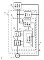
図4は、実施の形態1に係るノイズ抑制装置20の回路である。ノイズ抑制装置20(図の内側の点線の枠を参照)は、かかる電力変換システムのコモンモードノイズを低減させることを目的とし、ノイズフィルタ10(図の外側の点線の枠を参照)の一部ないしは全てを構成する。本実施の形態では、接地コンデンサ11とノイズ抑制装置20によってノイズフィルタ10を構成している。
FIG. 4 is a circuit of the noise suppression device 20 according to the first embodiment. The noise suppression device 20 (see the dotted line frame inside the figure) is a part of the noise filter 10 (see the dotted line frame outside the figure) for the purpose of reducing the common mode noise of the power conversion system. Or make up everything. In the present embodiment, the noise filter 10 is composed of the grounding capacitor 11 and the noise suppression device 20.
このノイズ抑制装置20は、ノイズなどの特定の信号を検出する検出回路30と、この検出回路30から検出された成分をもとに所望の波形信号を形成する波形信号形成回路40と、形成した波形信号をコモンモードへ送信する注入トランス50などで構成される信号送信器と、電力変換装置80、あるいは波形信号形成回路40自身の動作状態を検知する状態検知器60と、検知した信号に応じて所定の量、あるいは所定のタイミングだけゲインを調整するゲイン調整器70で構成される。
The noise suppression device 20 is formed by a detection circuit 30 that detects a specific signal such as noise, and a waveform signal forming circuit 40 that forms a desired waveform signal based on the components detected from the detection circuit 30. A signal transmitter including an injection transformer 50 that transmits a waveform signal to a common mode, a state detector 60 that detects the operating state of the power converter 80 or the waveform signal forming circuit 40 itself, and a state detector 60 that detects the detected signal. It is composed of a gain adjuster 70 that adjusts the gain by a predetermined amount or a predetermined timing.
図5は、実施の形態1、2、3、4、5に係る検出回路30の構成例であり、検出回路をコモンモードトランスで構成した場合を示す。検出トランスは、交流電源1と被制御装置である電力変換装置80間のRST相動力線に挿入され、R相巻線31、S相巻線32、T相巻線33は同相に巻かれている。このとき、ノーマルモードの発生磁束は相殺され、コモンモードの発生磁束は強め合うため、検出コイルは、コモンモードのみ高いインダクタンス値を備え、コモンモードチョークコイルとして働く。さらに、検出トランスを通過するコモンモードノイズ4によって、補助巻線34の両端に、ノイズ検出信号35が生じる。補助巻線の出力両端は、波形信号形成回路40へと接続される。
FIG. 5 is a configuration example of the detection circuit 30 according to the first, second, third, fourth, and fifth embodiments, and shows a case where the detection circuit is configured by a common mode transformer. The detection transformer is inserted into the RST phase power line between the AC power supply 1 and the power conversion device 80 which is the controlled device, and the R phase winding 31, the S phase winding 32, and the T phase winding 33 are wound in the same phase. There is. At this time, since the generated magnetic fluxes in the normal mode cancel each other out and the generated magnetic fluxes in the common mode strengthen each other, the detection coil has a high inductance value only in the common mode and acts as a common mode choke coil. Further, the common mode noise 4 passing through the detection transformer generates a noise detection signal 35 at both ends of the auxiliary winding 34. Both ends of the output of the auxiliary winding are connected to the waveform signal forming circuit 40.
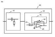
図6は、実施の形態1、2、3、4、5に係る波形信号形成回路の一例であり、帯域制限回路41と高周波増幅回路42で構成した場合を示す。帯域制限回路41はたとえば抵抗とコンデンサで構成されるパッシブフィルタにより、ノイズ補償に不要となる低周波成分を減衰させる。高周波増幅回路42は、たとえばオペアンプ45を用いて反転ないしは非反転増幅回路を形成し、帯域制限回路41によって不要成分をカットされた信号を、入力抵抗43と帰還抵抗44の比に応じて増幅させる。
FIG. 6 is an example of the waveform signal forming circuit according to the first, second, third, fourth, and fifth embodiments, and shows a case where the band limiting circuit 41 and the high frequency amplifier circuit 42 are configured. The band limiting circuit 41 attenuates low frequency components that are unnecessary for noise compensation by, for example, a passive filter composed of a resistor and a capacitor. The high-frequency amplifier circuit 42 forms an inverting or non-inverting amplifier circuit using, for example, an operational amplifier 45, and amplifies a signal whose unnecessary components are cut by the band limiting circuit 41 according to the ratio of the input resistor 43 and the feedback resistor 44. ..
図7は、実施の形態1、2、3、4、5に係る信号送信器の構成例であり、信号送信器をコモンモードトランスで構成した場合を示す。注入トランス50は、検出回路30と電力変換装置80間のRST相動力線に挿入され、R相巻線51、S相巻線52、T相巻線53は同相に巻かれている。ここで補助巻線54にノイズ注入信号55が入力され、R相巻線51、S相巻線52、T相巻線53のコモンモードに対して、(図示しない)コモンモードノイズを相殺するようなコモンモード注入電圧56が入力される。
FIG. 7 is a configuration example of the signal transmitter according to the first, second, third, fourth, and fifth embodiments, and shows a case where the signal transmitter is configured by a common mode transformer. The injection transformer 50 is inserted into the RST phase power line between the detection circuit 30 and the power conversion device 80, and the R phase winding 51, the S phase winding 52, and the T phase winding 53 are wound in the same phase. Here, a noise injection signal 55 is input to the auxiliary winding 54 so as to cancel the common mode noise (not shown) with respect to the common modes of the R-phase winding 51, the S-phase winding 52, and the T-phase winding 53. Common mode injection voltage 56 is input.
ここで、電力変換装置80が負荷急変などにより一時的な過負荷あるいは不平衡状態になる場合、負荷電流値が一時的に上昇するため、信号送信器に生じるノーマル成分の磁束が一時的に上昇する。信号送信器の1つである注入トランス50に生じる磁束は、漏れインダクタンスとノーマル電流の積により発生するノーマル成分の磁束と、ノイズ抑制装置の能動的な動作により生じるコモンモード成分の磁束の和である。このうちノーマル成分の磁束が上昇し、コア内の磁束密度が上昇する。
Here, when the power converter 80 is temporarily overloaded or unbalanced due to a sudden load change or the like, the load current value temporarily rises, so that the magnetic flux of the normal component generated in the signal transmitter temporarily rises. do. The magnetic flux generated in the injection transformer 50, which is one of the signal transmitters, is the sum of the magnetic flux of the normal component generated by the product of the leakage inductance and the normal current and the magnetic flux of the common mode component generated by the active operation of the noise suppression device. be. Of these, the magnetic flux of the normal component rises, and the magnetic flux density in the core rises.
換言すると、コアの磁気飽和を生じさせないためには、一時的な過負荷あるいは不平衡状態のノーマル成分磁束の上昇を考慮してコモンモードトランスのコア磁気設計を行わねばならず、コアのサイズは大きくなり、小型化、あるいは低コスト化の妨げとなる課題があった。
In other words, in order not to cause magnetic saturation of the core, the core magnetic design of the common mode transformer must be performed in consideration of the temporary overload or the rise of the normal component magnetic flux in the unbalanced state, and the core size is large. There was a problem that it became large and hindered miniaturization or cost reduction.
本実施の形態では、ノイズ抑制装置に備えた(図示しない)注入電流センサから出力される、注入電流の電流状態信号68aを状態検知器60に入力し、入力値が所定の閾値を超えた場合(例えば過電流の場合)に、ゲイン調整器70を用いてゲインを所定の時間だけ低下させることができる。これにより、コアに生じる磁束のうち、ノイズ抑制装置の能動的な動作により生じるコモンモード成分の磁束が一時的に減少し、コアの磁気飽和を回避することができる。なお、上記電流状態信号、及び後述する保護状態信号、特定状態信号、動作状態信号を総称して状態信号と呼ぶ。
In the present embodiment, when the current state signal 68a of the injection current output from the injection current sensor (not shown) provided in the noise suppression device is input to the state detector 60 and the input value exceeds a predetermined threshold value. (For example, in the case of overcurrent), the gain adjuster 70 can be used to reduce the gain by a predetermined time. As a result, among the magnetic flux generated in the core, the magnetic flux of the common mode component generated by the active operation of the noise suppression device is temporarily reduced, and the magnetic saturation of the core can be avoided. The current state signal, the protection state signal, the specific state signal, and the operation state signal, which will be described later, are collectively referred to as a state signal.
本願の構成要素を示す図8、および図9に従い、本実施の形態1の動作を説明する。
図8は、実施の形態1、2、3、4、5に係るゲイン調整器70の構成例であり、ゲイン調整器70をアップダウン式のデジタルポテンショメータで構成した場合を示す。ここでは、ゲイン調整器70は、制御IC71とデジタルポテンショメータ72で構成される。 The operation of the first embodiment will be described with reference to FIGS. 8 and 9 showing the components of the present application.
FIG. 8 shows a configuration example of thegain adjuster 70 according to the first, second, third, fourth, and fifth embodiments, and shows a case where the gain adjuster 70 is configured by an up-down type digital potentiometer. Here, the gain adjuster 70 is composed of a control IC 71 and a digital potentiometer 72.
図8は、実施の形態1、2、3、4、5に係るゲイン調整器70の構成例であり、ゲイン調整器70をアップダウン式のデジタルポテンショメータで構成した場合を示す。ここでは、ゲイン調整器70は、制御IC71とデジタルポテンショメータ72で構成される。 The operation of the first embodiment will be described with reference to FIGS. 8 and 9 showing the components of the present application.
FIG. 8 shows a configuration example of the
図9は、実施の形態1、2、3、4、5に係る図8のゲイン調整器70の構成例の動作の一例を示すものである。図8および図9中では状態検知器60が検知する信号の1つである状態検知信号60aを(ローレベルで有効となる)ローアクティブ信号DETECTで表記している。ローアクティブ信号DETECTは、タイミングt1でハイからローになって任意状態を検知し、タイミングt2でローからハイになって任意状態の検知を終了する。
FIG. 9 shows an example of the operation of the configuration example of the gain adjuster 70 of FIG. 8 according to the first, second, third, fourth, and fifth embodiments. In FIGS. 8 and 9, the state detection signal 60a, which is one of the signals detected by the state detector 60, is represented by the low active signal DETECT (which is valid at the low level). The low active signal DETECT changes from high to low at timing t1 to detect an arbitrary state, and changes from low to high at timing t2 to end the detection of the arbitrary state.
ここで、制御IC71は、タイミングt1でデジタルポテンショメータ72のチップセレクト信号73をハイ(抵抗値の切り替え不可状態)からロー(抵抗値の切り替え可能状態)に切り替えて、アップダウン制御入力74をハイ(アップカウント)からロー(ダウンカウント)に切り替える。ここで、制御IC71の3つの信号の論理はすべて負論理であり、ローレベルで有効となる。
Here, the control IC 71 switches the chip select signal 73 of the digital potentiometer 72 from high (a state in which the resistance value cannot be switched) to low (a state in which the resistance value can be switched) at timing t1, and sets the up / down control input 74 to high (a state in which the resistance value can be switched). Switch from (up count) to low (down count). Here, the logic of the three signals of the control IC 71 is all negative logic and is valid at a low level.
このときデジタルポテンショメータ72は、インクリメント制御入力75のハイからローの立下りに同期し、抵抗値76が、アップダウン制御入力74のハイ状態、あるいはロー状態に従って所定の分解能幅で上昇または低下する。
ここではアップダウン制御入力74がロー(ダウンカウント)のため、抵抗値76が低下し、高周波増幅回路42の増幅ゲインは低下する。その後、タイミングt2となり、インクリメント制御入力75がカウント停止しハイとなった後、チップセレクタ信号を所定の復帰時間77だけ遅延させてローからハイへと切り替え、低下した抵抗値76をデジタルポテンショメータの不揮発メモリへ記録することなく、抵抗値76を初期値へと復帰させる動作を行う。この復帰動作により、一時的に増加した増幅ゲインが、過電流状態の解除に伴い、所定の復帰時間後に再び元の値に復帰する。 At this time, thedigital potentiometer 72 synchronizes with the falling edge of the increment control input 75 from high to low, and the resistance value 76 rises or falls with a predetermined resolution width according to the high state or low state of the up / down control input 74.
Here, since the up / downcontrol input 74 is low (down count), the resistance value 76 decreases, and the amplification gain of the high frequency amplifier circuit 42 decreases. After that, at the timing t2, after the increment control input 75 stops counting and becomes high, the chip selector signal is delayed by a predetermined return time 77 to switch from low to high, and the lowered resistance value 76 is converted to the non-volatile value of the digital potentiometer. The operation of returning the resistance value 76 to the initial value is performed without recording in the memory. By this recovery operation, the temporarily increased amplification gain returns to the original value again after a predetermined recovery time as the overcurrent state is released.
ここではアップダウン制御入力74がロー(ダウンカウント)のため、抵抗値76が低下し、高周波増幅回路42の増幅ゲインは低下する。その後、タイミングt2となり、インクリメント制御入力75がカウント停止しハイとなった後、チップセレクタ信号を所定の復帰時間77だけ遅延させてローからハイへと切り替え、低下した抵抗値76をデジタルポテンショメータの不揮発メモリへ記録することなく、抵抗値76を初期値へと復帰させる動作を行う。この復帰動作により、一時的に増加した増幅ゲインが、過電流状態の解除に伴い、所定の復帰時間後に再び元の値に復帰する。 At this time, the
Here, since the up / down
ここで、電力変換装置80において負荷変動などの要因により、一時的な過負荷状態が生じるとき、信号送信器の1つである注入トランス50におけるコア磁束について、ノーマルモード成分の磁束が一時的に増加してしまうため、コアの磁束飽和を避けるためには、一時的な過負荷状態も考慮のうえ、コアの磁束設計をしなければならなかった。
Here, when a temporary overload state occurs in the power converter 80 due to factors such as load fluctuations, the magnetic flux of the normal mode component is temporarily generated with respect to the core magnetic flux in the injection transformer 50, which is one of the signal transmitters. Therefore, in order to avoid the magnetic flux saturation of the core, it was necessary to design the magnetic flux of the core in consideration of the temporary overload state.
本願では、被制御装置である電力変換装置80から得られる電流状態信号68bを状態検知器60に入力し、入力値が所定の閾値を超えた場合に、ゲイン調整器70を用いてゲインを所定の時間低下させ、保護状態が解除されたのちに所定の復帰時間をもって増幅ゲインを再び元の値に戻すことができる。これにより、信号送信器の1つである注入トランス50のコアの磁束設計において、一時的な過負荷状態による設計制約を生じさせず、ノイズ補償動作を実現することができる。
In the present application, the current state signal 68b obtained from the power conversion device 80, which is a controlled device, is input to the state detector 60, and when the input value exceeds a predetermined threshold value, the gain is determined by using the gain adjuster 70. After the protection state is released, the amplification gain can be returned to the original value again with a predetermined recovery time. As a result, in the magnetic flux design of the core of the injection transformer 50, which is one of the signal transmitters, the noise compensation operation can be realized without causing design restrictions due to a temporary overload state.
以上より、電力変換装置80が一時的な過電流になり、コモンモードとノーマルモードの和で示されるコア磁束のうちノーマルモード成分の磁束が一時的に増加した場合、波形信号形成回路によって注入トランスに送信されるコモンモード成分の磁束を一時的に低下させることによってコアの最大磁束密度を低減することで、コアサイズを小型化することができ、ノイズ抑制装置の小型化および低コスト化を実現することができる。
From the above, when the power converter 80 becomes a temporary overcurrent and the magnetic flux of the normal mode component among the core magnetic fluxes represented by the sum of the common mode and the normal mode temporarily increases, the injection transformer is provided by the waveform signal forming circuit. By temporarily reducing the magnetic flux of the common mode component transmitted to the core to reduce the maximum magnetic flux density of the core, the core size can be reduced, and the noise suppression device can be made smaller and the cost can be reduced. can do.
なお、電流センサ出力は、ノイズ抑制装置が備えるものでもよく、直接的な電流の検出量でなく、装置からのI/O信号(たとえば過電流状態通知信号、負荷急変通知信号など)であってもよい。
The current sensor output may be provided in the noise suppression device, and is not a direct current detection amount but an I / O signal (for example, an overcurrent state notification signal, a load sudden change notification signal, etc.) from the device. May be good.
なお、帯域制限回路は低周波を抑制するハイパスフィルタのみならず、高周波を抑制するローパスフィルタ、特定帯域を抑制するノッチフィルタ、特定帯域を通過させるバンドパスフィルタなど、本願の趣旨を逸脱しない範囲で自由に構成することができる。また、高周波増幅回路は、オペアンプをもちいた反転増幅回路、非反転増幅回路など、本願の趣旨を逸脱しない範囲で自由に構成することができる。
The band limiting circuit includes not only a high-pass filter that suppresses low frequencies, but also a low-pass filter that suppresses high frequencies, a notch filter that suppresses a specific band, a band-pass filter that passes a specific band, and the like within a range that does not deviate from the purpose of the present application. It can be configured freely. Further, the high-frequency amplifier circuit can be freely configured within a range that does not deviate from the gist of the present application, such as an inverting amplifier circuit using an operational amplifier and a non-inverting amplifier circuit.
また、本実施の形態の構成は、三相三線式の電力変換システムのみならず、三相四線式の電力変換システムであってもよい。さらに、ゲイン調整器は、制御ICと通信インターフェースを持つデジタルポテンショメータの組合せ、アナログ回路網とアップダウン式デジタルポテンショメータの組合せ、あるいは半導体スイッチを用いた抵抗短絡回路ないしは異なるアナログ制御回路網同士のロードスイッチの切り替えによる抵抗およびコンデンサ容量値の切り替え、抵抗値を可変できる電子抵抗による抵抗値の切り替えなど、本願の趣旨を逸脱しない範囲で自由に構成することができる。
Further, the configuration of the present embodiment may be not only a three-phase three-wire power conversion system but also a three-phase four-wire power conversion system. Further, the gain adjuster is a combination of a control IC and a digital potentiometer having a communication interface, a combination of an analog network and an up-down digital potentiometer, a resistance short circuit using a semiconductor switch, or a load switch between different analog control networks. It can be freely configured within a range that does not deviate from the gist of the present application, such as switching the resistance and capacitor capacitance value by switching between the two, and switching the resistance value by an electronic resistance whose resistance value can be changed.
実施の形態2.
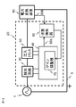
図10は、実施の形態2に係るノイズ抑制装置20の回路である。
実施の形態2に係るノイズ抑制装置20が、実施の形態1に係るノイズ抑制装置20と異なる点は、状態検知器60に入力される信号が、電流状態信号68aの代わりに保護状態信号65となる点である。Embodiment 2.
FIG. 10 is a circuit of thenoise suppression device 20 according to the second embodiment.
The difference between thenoise suppression device 20 according to the second embodiment and the noise suppression device 20 according to the first embodiment is that the signal input to the state detector 60 is a protection state signal 65 instead of the current state signal 68a. It is a point.
図10は、実施の形態2に係るノイズ抑制装置20の回路である。
実施の形態2に係るノイズ抑制装置20が、実施の形態1に係るノイズ抑制装置20と異なる点は、状態検知器60に入力される信号が、電流状態信号68aの代わりに保護状態信号65となる点である。
FIG. 10 is a circuit of the
The difference between the
ここで、波形信号形成回路40において何らかの理由で注入電流が過電流となる場合(たとえば雷サージ等の外来ノイズ侵入によりノイズ注入手段である信号送信器のコモンモードトランスが瞬時磁気飽和を起こした場合)、波形信号形成回路40の回路部品保護のために、装置動作を停止する必要がある。しかし、波形信号形成回路40の回路部品に保護回路内蔵の部品を選定することで、この動作を実現する場合、一般に保護回路内蔵部品は高価であることと、ラインナップ上の制約があり、設計制約が生じてしまう課題があった。
Here, when the injection current becomes an overcurrent in the waveform signal forming circuit 40 for some reason (for example, when the common mode transformer of the signal transmitter which is a noise injection means causes instantaneous magnetic saturation due to the intrusion of external noise such as a lightning surge). ), It is necessary to stop the operation of the device in order to protect the circuit components of the waveform signal forming circuit 40. However, when this operation is realized by selecting a component with a built-in protection circuit as the circuit component of the waveform signal forming circuit 40, the component with a built-in protection circuit is generally expensive and there are restrictions on the lineup, so there are design restrictions. There was a problem that caused.
図11は、実施の形態1、2、3、4、5に係る状態検知器60の構成例であり、状態検知器60を、単体の注入電流の過電流検出回路で構成した場合を示す。ここでは、波形信号形成回路40の出力と信号送信器の1つである注入トランス50の入力に対して、直列に挿入されたシャント抵抗61と、注入電流値に比例してシャント抵抗の両端に生じる注入電流検出電圧を所定の閾値と比較するコンパレータ62と、コンパレータ62に所定の閾値を供給する閾値作成回路63とで構成され、コンパレータ62の出力が注入電流の過電流検出信号となる。
FIG. 11 is a configuration example of the state detector 60 according to the first, second, third, fourth, and fifth embodiments, and shows a case where the state detector 60 is configured by a single injection current overcurrent detection circuit. Here, the shunt resistance 61 inserted in series with respect to the output of the waveform signal forming circuit 40 and the input of the injection transformer 50, which is one of the signal transmitters, and both ends of the shunt resistance in proportion to the injection current value. It is composed of a comparator 62 that compares the generated injection current detection voltage with a predetermined threshold, and a threshold creation circuit 63 that supplies a predetermined threshold to the comparator 62, and the output of the comparator 62 becomes an overcurrent detection signal of the injection current.
この他、状態検知器60には、被制御装置である電力変換装置80から特定の状態を示す特定状態信号66(たとえば装置が過負荷状態であることを示す過負荷状態検出信号)をI/Oポートより受け取るインターフェース回路が追加されていてもよい。さらには、注入回路の発熱部品を冷却するための冷却フィンに具備したサーミスタからの過熱状態検出信号を受け取るインターフェース回路が追加されてもよい。
In addition, the state detector 60 receives a specific state signal 66 (for example, an overload state detection signal indicating that the device is in an overload state) indicating a specific state from the power conversion device 80 which is a controlled device. An interface circuit that receives from the O port may be added. Further, an interface circuit for receiving an overheat state detection signal from the thermistor provided in the cooling fin for cooling the heat generating component of the injection circuit may be added.
本実施の形態のノイズ抑制装置では、波形信号形成回路40に備えた安価なシャント抵抗61などの適宜の手段によって得られる保護状態信号65を状態検知器60に入力し、入力値が所定の閾値を超えた場合に、ゲイン調整器70を用いてゲインを所定の時間低下させ、保護状態が解除されたのちに所定の復帰時間をもって増幅ゲインを再び元の値に戻すことができる。
In the noise suppression device of the present embodiment, the protection state signal 65 obtained by an appropriate means such as an inexpensive shunt resistor 61 provided in the waveform signal forming circuit 40 is input to the state detector 60, and the input value is a predetermined threshold value. When the value exceeds, the gain adjuster 70 can be used to reduce the gain for a predetermined time, and after the protection state is released, the amplification gain can be returned to the original value again with a predetermined recovery time.
これにより、波形信号形成回路40の回路部品の選定において、設計制約を生じさせず、保護動作を実現することができる。
This makes it possible to realize a protective operation without causing design restrictions in the selection of circuit components of the waveform signal forming circuit 40.
以上より、コアの磁気飽和が生じてノイズ補償用の注入電流が過電流になったときに、コモンモード成分とノーマルモード成分の和で示されるコア磁束のうち、コモンモード成分の磁束を一時的に減少させることによってコアの最大磁束密度を低減することで、コアサイズを小型化することができ、ノイズ抑制装置の小型化および低コスト化を実現することができる。
From the above, when the magnetic saturation of the core occurs and the injection current for noise compensation becomes an overcurrent, the magnetic flux of the common mode component among the core magnetic fluxes indicated by the sum of the common mode component and the normal mode component is temporarily used. By reducing the maximum magnetic flux density of the core, the core size can be reduced, and the noise suppression device can be reduced in size and cost.
実施の形態3.
実施の形態3は、図10に示す実施の形態2の変形例である。
実施の形態3に係るノイズ抑制装置20が、実施の形態2に係るノイズ抑制装置20と異なる点は、保護状態信号を検知したのちの、ゲイン調整器70の動作について、所定の復帰時間経過後に、直ちに元の増幅ゲインに復帰させずに、段階的に増幅ゲインを微小値まで下げたのちに、再び上昇させて復帰に至る点である。Embodiment 3.
The third embodiment is a modification of the second embodiment shown in FIG.
The difference between thenoise suppression device 20 according to the third embodiment and the noise suppression device 20 according to the second embodiment is that the operation of the gain adjuster 70 after the detection of the protection state signal is performed after a predetermined recovery time has elapsed. The point is that the amplification gain is gradually lowered to a minute value without immediately returning to the original amplification gain, and then raised again to reach the recovery.
実施の形態3は、図10に示す実施の形態2の変形例である。
実施の形態3に係るノイズ抑制装置20が、実施の形態2に係るノイズ抑制装置20と異なる点は、保護状態信号を検知したのちの、ゲイン調整器70の動作について、所定の復帰時間経過後に、直ちに元の増幅ゲインに復帰させずに、段階的に増幅ゲインを微小値まで下げたのちに、再び上昇させて復帰に至る点である。
The third embodiment is a modification of the second embodiment shown in FIG.
The difference between the
ここで、波形信号形成回路40の何らかの保護動作によりノイズ抑制装置20の出力が遮断された場合を考える。このとき、出力遮断直前のコア磁性材のヒステリシス特性にしたがって、コア内部には残留磁束が生じる。保護動作の働いた原因が取り除かれ、ノイズ抑制装置20が再び出力を始めるとすると、通常のゲインでノイズ抑制装置が動作すると、通常生じる磁束に残留磁束が加わることで、コモンモードトランスコアの磁気飽和の恐れがある。コア磁性材中でも、高い透磁率のコア、たとえばファインメット等の高透磁率のナノ結晶磁性材では、一般的なフェライト材と比べて残留磁束が大きいため、問題となる。
Here, consider a case where the output of the noise suppression device 20 is cut off by some kind of protection operation of the waveform signal forming circuit 40. At this time, a residual magnetic flux is generated inside the core according to the hysteresis characteristic of the core magnetic material immediately before the output is cut off. Assuming that the cause of the protective operation is removed and the noise suppression device 20 starts outputting again, when the noise suppression device operates at a normal gain, the residual magnetic flux is added to the normally generated magnetic flux, so that the magnetism of the common mode transformer core There is a risk of saturation. Among the core magnetic materials, a core having a high magnetic permeability, for example, a nanocrystalline magnetic material having a high magnetic permeability such as Finemet, has a problem because the residual magnetic flux is larger than that of a general ferrite material.
本願では、ノイズ抑制装置20が再始動する際に、波形信号形成回路40の補償ゲインを、保護動作がはたらく以前の値に戻す際に、段階的に増幅ゲインを微小値まで低下させる動作を行うことで残留磁束を消磁することができる。
In the present application, when the noise suppression device 20 is restarted, the compensation gain of the waveform signal forming circuit 40 is returned to the value before the protection operation is activated, and the amplification gain is gradually reduced to a minute value. As a result, the residual magnetic flux can be demagnetized.
これにより、磁気飽和によるラッシュ電流の発生を回避することによって、残留磁束の大きなコア磁性材を適用することができる。また、ノイズ抑制装置20が保護動作による遮断後、再び出力を開始する際に、補償ゲインを所定の時間をかけて段階的に上昇させることで、波形信号形成回路40をソフトスタートさせ、回路消費電流のオーバーシュートを抑制し、回路電源容量の低減を図ることができる。
This makes it possible to apply a core magnetic material having a large residual magnetic flux by avoiding the generation of a rush current due to magnetic saturation. Further, when the noise suppression device 20 starts output again after being cut off by the protection operation, the compensation gain is gradually increased over a predetermined time to soft-start the waveform signal forming circuit 40 and consume the circuit. It is possible to suppress current overshoot and reduce the circuit power supply capacity.
実施の形態4.
図12は、実施の形態4に係るノイズ抑制装置の回路である。
実施の形態4に係るノイズ抑制装置20が、実施の形態2に係るノイズ抑制装置20と異なる点は、状態検知器60に入力される信号が、保護状態信号65の代わりに動作状態信号69aとなる点である。Embodiment 4.
FIG. 12 is a circuit of the noise suppression device according to the fourth embodiment.
The difference between thenoise suppression device 20 according to the fourth embodiment and the noise suppression device 20 according to the second embodiment is that the signal input to the state detector 60 is an operating state signal 69a instead of the protection state signal 65. It is a point.
図12は、実施の形態4に係るノイズ抑制装置の回路である。
実施の形態4に係るノイズ抑制装置20が、実施の形態2に係るノイズ抑制装置20と異なる点は、状態検知器60に入力される信号が、保護状態信号65の代わりに動作状態信号69aとなる点である。
FIG. 12 is a circuit of the noise suppression device according to the fourth embodiment.
The difference between the
ここで、電力変換装置80が複数の運転モードを持っている場合、装置の運転モードが切り替わると、半導体スイッチのスイッチングパターンが変化することにより、一般にノイズの振幅と発生周波数が変化し、ノイズ規格を満たすためにノイズ抑制装置20に必要となる減衰量、あるいは周波数特性が変化してしまう。
Here, when the power conversion device 80 has a plurality of operation modes, when the operation modes of the devices are switched, the switching pattern of the semiconductor switch changes, so that the amplitude of noise and the generated frequency generally change, and the noise standard. The amount of attenuation required for the noise suppression device 20 or the frequency characteristic changes in order to satisfy the above conditions.
このため、すべての運転モードに対応したノイズ抑制装置20の設計を行うことは難しく、ノイズ抑制装置20の回路部品定格ならびに回路電源容量の低減、あるいはノイズ抑制効果の最大化の妨げとなっていた。
Therefore, it is difficult to design the noise suppression device 20 corresponding to all operation modes, which hinders the reduction of the circuit component rating and the circuit power supply capacity of the noise suppression device 20 or the maximization of the noise suppression effect. ..
本実施の形態では、電力変換装置80から得られる動作状態信号69bを状態検知器60に入力し、ゲイン調整器70を用いて、波形信号形成回路40の増幅ゲインを動作状態信号69bの値に応じた所定の増幅ゲインに変化させることができる。
In the present embodiment, the operating state signal 69b obtained from the power converter 80 is input to the state detector 60, and the gain adjuster 70 is used to set the amplification gain of the waveform signal forming circuit 40 to the value of the operating state signal 69b. It can be changed to a predetermined amplification gain according to the situation.
これにより、波形信号形成回路40および信号送信器の1つである注入トランス50のコアの磁束設計において、運転モードによるノイズ抑制装置20の設計制約を生じさせず、ノイズ補償動作を実現することができる。
As a result, in the magnetic flux design of the core of the waveform signal forming circuit 40 and the injection transformer 50 which is one of the signal transmitters, the noise compensation operation can be realized without causing the design constraint of the noise suppression device 20 depending on the operation mode. can.
以上より、電力変換装置80が異なるノイズ振幅と発生周波数をもつ複数の運転モードを持っている場合に、それぞれのノイズ振幅と発生周波数のパターンに応じて、波形信号形成回路40の増幅ゲインを動作状態信号69aの値に応じた所定の増幅ゲインに変化させることによって、波形信号形成回路40および信号送信器の1つである注入トランス50のコアサイズを小型化することができ、ノイズ抑制装置20の回路部品定格ならびに回路電源容量を低減するとともに、ノイズ抑制効果を最大化することができる。
From the above, when the power converter 80 has a plurality of operation modes having different noise amplitudes and generation frequencies, the amplification gain of the waveform signal forming circuit 40 is operated according to each noise amplitude and generation frequency pattern. By changing the amplification gain to a predetermined value according to the value of the state signal 69a, the core size of the waveform signal forming circuit 40 and the injection transformer 50, which is one of the signal transmitters, can be reduced, and the noise suppression device 20 can be reduced in size. The noise suppression effect can be maximized while reducing the circuit component rating and circuit power supply capacity.
実施の形態5.
実施の形態5は、実施の形態1、2、3、4の変形例である。
ここで、上記の実施の形態1による波形信号形成回路40の保護動作について、典型的には、装置、あるいはトランスの発熱により、ノイズ量ないしはノイズの周波数帯域が異なるものに推移した場合、最適な補償ゲインが変化することで、連続して保護動作が働き続ける恐れがある。 Embodiment 5.
The fifth embodiment is a modification of the first, second, third, and fourth embodiments.
Here, regarding the protection operation of the waveformsignal forming circuit 40 according to the first embodiment, typically, when the amount of noise or the frequency band of noise changes due to heat generation of the device or a transformer, it is optimal. As the compensation gain changes, the protection operation may continue to work.
実施の形態5は、実施の形態1、2、3、4の変形例である。
ここで、上記の実施の形態1による波形信号形成回路40の保護動作について、典型的には、装置、あるいはトランスの発熱により、ノイズ量ないしはノイズの周波数帯域が異なるものに推移した場合、最適な補償ゲインが変化することで、連続して保護動作が働き続ける恐れがある。 Embodiment 5.
The fifth embodiment is a modification of the first, second, third, and fourth embodiments.
Here, regarding the protection operation of the waveform
これを回避するためには、典型的には、熱、あるいは電気的条件上のロバスト性も考慮のうえ、ノイズ減衰量、あるいは回路電源容量を設計せねばならず、小型化あるいは低コスト化の妨げとなっていた。
In order to avoid this, it is typically necessary to design the noise attenuation amount or circuit power supply capacity in consideration of robustness under thermal or electrical conditions, resulting in miniaturization or cost reduction. It was a hindrance.
本実施の形態では、所定の時間幅内で所定の回数以上、連続して保護動作が働いた場合に、最適な増幅ゲインが低い値に変化したとみなし、ゲイン調整器70によって所定の幅だけ増幅ゲインを恒久的に低下させる。
In the present embodiment, when the protection operation is continuously performed a predetermined number of times or more within a predetermined time width, it is considered that the optimum amplification gain has changed to a low value, and the gain adjuster 70 determines only the predetermined width. Permanently reduce the amplification gain.
実現手段としては、図10に示した実施形態1の動作例とは異なり、所定の復帰時間の経過後に、インクリメント制御入力75をロー状態ではなくハイ状態のまま、チップセレクト信号73を立ち上げることにより、ゲイン調整器70のデジタルポテンショメータ72(図8参照)の設定抵抗値の設定を不揮発メモリに書き込むことで、恒久的に増幅ゲインを所定の幅だけ低下させる。
As a means for realizing this, unlike the operation example of the first embodiment shown in FIG. 10, after the lapse of a predetermined recovery time, the chip select signal 73 is started up while the increment control input 75 is not in the low state but in the high state. By writing the set resistance value setting of the digital potentiometer 72 (see FIG. 8) of the gain adjuster 70 to the non-volatile memory, the amplification gain is permanently reduced by a predetermined width.
さらには、所定の時間幅内で、保護動作が一切働かない場合に、最適な増幅ゲインがより高い値にあるとみなし、ゲイン調整器によって所定の幅だけ増幅ゲインを恒久的に増加させることもできる。これにより、小型でかつ低コストであり、ロバストなノイズ抑制装置を実現させることができる。
Furthermore, if the protection operation does not work at all within a predetermined time width, the optimum amplification gain is considered to be at a higher value, and the gain adjuster can permanently increase the amplification gain by a predetermined width. can. As a result, a compact, low-cost, and robust noise suppression device can be realized.
なお、本願のノイズ抑制装置の信号処理に係るハードウエア92の一例を図13に示す。この図に示すように、本装置の信号処理に係るハードウエア92(具体的には、図4、図10、図12に示す波形信号形成回路40、あるいは状態検知器60の少なくとも一部が該当する)には、プロセッサ93と記憶装置94が含まれる。記憶装置は図示していないが、ランダムアクセスメモリ等の揮発性記憶装置と、フラッシュメモリ等の不揮発性の補助記憶装置とを具備する。また、フラッシュメモリの代わりにハードディスクの補助記憶装置を具備してもよい。プロセッサ93は、記憶装置94から入力されたプログラムを実行する。この場合、補助記憶装置から揮発性記憶装置を介してプロセッサ93にプログラムが入力される。また、プロセッサ93は、演算結果等のデータを記憶装置94の揮発性記憶装置に出力してもよいし、揮発性記憶装置を介して補助記憶装置にデータを保存してもよい。
FIG. 13 shows an example of the hardware 92 related to the signal processing of the noise suppression device of the present application. As shown in this figure, at least a part of the hardware 92 related to the signal processing of the present apparatus (specifically, the waveform signal forming circuit 40 shown in FIGS. 4, 10 and 12 or the state detector 60 is applicable. Includes a processor 93 and a storage device 94. Although the storage device is not shown, it includes a volatile storage device such as a random access memory and a non-volatile auxiliary storage device such as a flash memory. Further, an auxiliary storage device of a hard disk may be provided instead of the flash memory. The processor 93 executes the program input from the storage device 94. In this case, the program is input from the auxiliary storage device to the processor 93 via the volatile storage device. Further, the processor 93 may output data such as a calculation result to the volatile storage device of the storage device 94, or may store the data in the auxiliary storage device via the volatile storage device.
1 交流電源、2 交流電源と電力変換装置間の電源線、3 接地線、4 コモンモードノイズ、10 ノイズフィルタ、11 接地コンデンサ、20 ノイズ抑制装置、30 検出回路、31、51 R相巻線、32、52 S相巻線、33、53 T相巻線、34、54 補助巻線、35 ノイズ検出信号、40 波形信号形成回路、41 帯域制限回路、42 高周波増幅回路、43 入力抵抗、44 帰還抵抗、45 オペアンプ、50 注入トランス、55 ノイズ注入信号、56 コモンモード注入電圧、60 状態検知器、60a 状態検知信号、61 シャント抵抗(電流検出抵抗)、62 コンパレータ、63 閾値作成回路、65 保護状態信号、66 特定状態信号、68a、68b 電流状態信号、69a、69b 動作状態信号、70 ゲイン調整器、71 制御IC、72 デジタルポテンショメータ、73 チップセレクト信号、74 アップダウン制御入力、75 インクリメント制御入力、76 抵抗値、77 復帰時間、80 電力変換装置、81、91 対地寄生容量、82a、82b、84a、84b、86a、86b 半導体スイッチ、83 U相上下アーム、85 V相上下アーム、87 W相上下アーム、88 インバータ出力端、89 インバータ直流電源、90 負荷、92 ハードウエア、93 プロセッサ、94 記憶装置、100 電力変換システム、Vcm コモンモード電圧
1 AC power supply, 2 Power supply line between AC power supply and power converter, 3 Ground line, 4 Common mode noise, 10 Noise filter, 11 Ground capacitor, 20 Noise suppression device, 30 Detection circuit, 31, 51 R-phase winding, 32, 52 S-phase winding, 33, 53 T-phase winding, 34, 54 auxiliary winding, 35 noise detection signal, 40 waveform signal formation circuit, 41 band limiting circuit, 42 high-voltage amplification circuit, 43 input resistance, 44 feedback Resistance, 45 optotype, 50 injection transformer, 55 noise injection signal, 56 common mode injection voltage, 60 state detector, 60a state detection signal, 61 shunt resistance (current detection resistance), 62 comparator, 63 threshold creation circuit, 65 protection state Signal, 66 specific state signal, 68a, 68b current state signal, 69a, 69b operation state signal, 70 gain adjuster, 71 control IC, 72 digital potential meter, 73 chip select signal, 74 up / down control input, 75 increment control input, 76 resistance value, 77 return time, 80 power converter, 81, 91 ground parasitic capacitance, 82a, 82b, 84a, 84b, 86a, 86b semiconductor switch, 83 U-phase up / down arm, 85 V-phase up / down arm, 87 W-phase up / down Arm, 88 inverter output end, 89 inverter DC power supply, 90 load, 92 hardware, 93 processor, 94 storage device, 100 power conversion system, Vcm common mode voltage
Claims (10)
- 交流電源と被制御装置との間に配置され、前記被制御装置に信号を送信するノイズ抑制装置であって、
特定の信号を検出する検出回路と、
この検出回路により検出された特定の信号から所定の波形信号を形成する波形信号形成回路と、
当該波形信号形成回路により形成された波形信号を前記被制御装置に送信する信号送信器と、
前記被制御装置、あるいは前記波形信号形成回路の状態を表す状態信号を検知する状態検知器と、
前記波形信号形成回路に内蔵され、前記状態検知器により検知した前記状態信号のいずれか一に応じて、前記波形信号のゲインを調整するゲイン調整器と、
を備え、
前記ゲイン調整器で調整された波形信号を前記被制御装置に送信することを特徴とするノイズ抑制装置。 A noise suppression device that is arranged between an AC power supply and a controlled device and transmits a signal to the controlled device.
A detection circuit that detects a specific signal and
A waveform signal forming circuit that forms a predetermined waveform signal from a specific signal detected by this detection circuit, and
A signal transmitter that transmits the waveform signal formed by the waveform signal forming circuit to the controlled device, and
A state detector that detects a state signal representing the state of the controlled device or the waveform signal forming circuit, and
A gain adjuster built in the waveform signal forming circuit and adjusting the gain of the waveform signal according to any one of the state signals detected by the state detector.
With
A noise suppression device characterized in that a waveform signal adjusted by the gain adjuster is transmitted to the controlled device. - 前記状態検知器が波形信号形成回路に過電流が生じたことを検知した場合に、前記過電流の検知時に前記波形信号のゲインを一時的に低下させるとともに、過電流状態が解消された後に前記波形信号のゲインを前記過電流の検知時の大きさに戻すことを特徴とする請求項1に記載のノイズ抑制装置。 When the state detector detects that an overcurrent has occurred in the waveform signal forming circuit, the gain of the waveform signal is temporarily lowered at the time of detecting the overcurrent, and after the overcurrent state is resolved, the above-mentioned The noise suppression device according to claim 1, wherein the gain of the waveform signal is returned to the magnitude at the time of detecting the overcurrent.
- 前記状態検知器は、前記被制御装置に接続された負荷が過負荷状態であることを検知した場合に、前記過負荷状態の検知時に前記波形信号のゲインを一時的に低下させるとともに、前記過負荷状態が解消された後に前記過負荷状態の検知時の前記波形信号のゲインに戻すことを特徴とする請求項1に記載のノイズ抑制装置。 When the state detector detects that the load connected to the controlled device is in an overloaded state, the state detector temporarily reduces the gain of the waveform signal at the time of detecting the overloaded state, and at the same time, the overloaded state is detected. The noise suppression device according to claim 1, wherein the gain of the waveform signal at the time of detecting the overload state is returned after the load state is released.
- 前記被制御装置が一時的に動作を停止、または、前記波形信号形成回路が前記状態検知器から入力される前記波形信号形成回路の保護信号により一時的に動作を停止した後に、停止した前記被制御装置、あるいは停止した前記波形信号形成回路の再起動を行う場合、前記ゲイン調整器にゲインを段階的に低下させる動作を行わせた後、段階的に上昇させる動作を行わせることを特徴とする請求項1に記載のノイズ抑制装置。 The controlled device is temporarily stopped, or the waveform signal forming circuit is temporarily stopped by a protection signal of the waveform signal forming circuit input from the state detector, and then stopped. When restarting the control device or the stopped waveform signal forming circuit, the gain adjuster is made to perform an operation of gradually lowering the gain and then gradually increasing the gain. The noise suppression device according to claim 1.
- 前記被制御装置が複数の運転モードを持つ場合において、前記状態検知器が、前記被制御装置の運転モードが切り替わったことを検知した場合、前記ゲイン調整器が前記波形信号のゲインを各運転モードに応じたゲインに変化させることを特徴とする請求項1に記載のノイズ抑制装置。 When the controlled device has a plurality of operation modes and the state detector detects that the operation mode of the controlled device has been switched, the gain adjuster adjusts the gain of the waveform signal to each operation mode. The noise suppression device according to claim 1, wherein the gain is changed according to the above.
- 前記波形信号形成回路について、設定した時間以内に所定の回数以上の保護信号を検知した場合に、前記ゲイン調整器が前記波形信号のゲインを所定値幅だけ低下させた値に切り替え、所定の時間を超えて保護動作が生じない場合に、ゲイン調整器が前記波形信号のゲインを所定値幅だけ増加させた値に切り替えることを特徴とする請求項1に記載のノイズ抑制装置。 When the waveform signal forming circuit detects a protection signal more than a predetermined number of times within a set time, the gain adjuster switches the gain of the waveform signal to a value reduced by a predetermined value range, and sets the predetermined time. The noise suppression device according to claim 1, wherein the gain adjuster switches the gain of the waveform signal to a value increased by a predetermined value range when the protection operation does not occur beyond the limit.
- 前記検出回路および前記信号送信器は、コモンモードトランスで構成されることを特徴とする請求項1に記載のノイズ抑制装置。 The noise suppression device according to claim 1, wherein the detection circuit and the signal transmitter are composed of a common mode transformer.
- 前記波形信号形成回路は、帯域制限回路と高周波増幅回路で構成されることを特徴とする請求項1に記載のノイズ抑制装置。 The noise suppression device according to claim 1, wherein the waveform signal forming circuit is composed of a band limiting circuit and a high frequency amplifier circuit.
- 前記状態検知器は、前記信号送信器に対して直列に接続されたシャント抵抗と、当該シャント抵抗の両端に生ずる電圧を所定の閾値と比較するコンパレータと、当該コンパレータに前記所定の閾値を与える閾値作成回路と、を備えることを特徴とする請求項1に記載のノイズ抑制装置。 The state detector includes a shunt resistor connected in series with the signal transmitter, a comparator that compares the voltage generated across the shunt resistor with a predetermined threshold value, and a threshold value that gives the comparator the predetermined threshold value. The noise suppression device according to claim 1, further comprising a creation circuit.
- 前記ゲイン調整器は、異なる制御回路網同士を切り替えるロードスイッチ、回路部品を短絡させて定数を変化させる半導体スイッチ、抵抗値を可変できる電子抵抗のいずれかで構成されることを特徴とする請求項1に記載のノイズ抑制装置。 The claim is characterized in that the gain adjuster is composed of any of a load switch for switching between different control networks, a semiconductor switch for short-circuiting circuit components to change a constant, and an electronic resistance whose resistance value can be changed. The noise suppression device according to 1.
Priority Applications (3)
| Application Number | Priority Date | Filing Date | Title |
|---|---|---|---|
| JP2021518024A JP6906731B1 (en) | 2020-02-17 | 2020-02-17 | Noise suppression device |
| DE112020006741.6T DE112020006741T5 (en) | 2020-02-17 | 2020-02-17 | INTERFERENCE SUPPRESSION DEVICE |
| PCT/JP2020/005972 WO2021166018A1 (en) | 2020-02-17 | 2020-02-17 | Noise suppression device |
Applications Claiming Priority (1)
| Application Number | Priority Date | Filing Date | Title |
|---|---|---|---|
| PCT/JP2020/005972 WO2021166018A1 (en) | 2020-02-17 | 2020-02-17 | Noise suppression device |
Publications (1)
| Publication Number | Publication Date |
|---|---|
| WO2021166018A1 true WO2021166018A1 (en) | 2021-08-26 |
Family
ID=76918289
Family Applications (1)
| Application Number | Title | Priority Date | Filing Date |
|---|---|---|---|
| PCT/JP2020/005972 WO2021166018A1 (en) | 2020-02-17 | 2020-02-17 | Noise suppression device |
Country Status (3)
| Country | Link |
|---|---|
| JP (1) | JP6906731B1 (en) |
| DE (1) | DE112020006741T5 (en) |
| WO (1) | WO2021166018A1 (en) |
Cited By (3)
| Publication number | Priority date | Publication date | Assignee | Title |
|---|---|---|---|---|
| WO2023054660A1 (en) * | 2021-09-30 | 2023-04-06 | ダイキン工業株式会社 | Noise reduction circuit, power conversion device and refrigeration device |
| WO2023105687A1 (en) * | 2021-12-08 | 2023-06-15 | 三菱電機株式会社 | Noise filter |
| WO2024075267A1 (en) * | 2022-10-07 | 2024-04-11 | 三菱電機株式会社 | Noise filter, power conversion system, and management system |
Citations (5)
| Publication number | Priority date | Publication date | Assignee | Title |
|---|---|---|---|---|
| JP2004357421A (en) * | 2003-05-29 | 2004-12-16 | Matsushita Electric Ind Co Ltd | Noise suppresser |
| JP2004357447A (en) * | 2003-05-30 | 2004-12-16 | Meidensha Corp | Noise reduction device of power conversion apparatus |
| JP2005204395A (en) * | 2004-01-14 | 2005-07-28 | Sanken Electric Co Ltd | Noise reduction apparatus and power converter |
| JP2010057268A (en) * | 2008-08-28 | 2010-03-11 | Fuji Electric Systems Co Ltd | Conductive noise filter |
| WO2011125944A1 (en) * | 2010-04-05 | 2011-10-13 | 三菱電機株式会社 | Leakage current reducing device |
-
2020
- 2020-02-17 JP JP2021518024A patent/JP6906731B1/en active Active
- 2020-02-17 WO PCT/JP2020/005972 patent/WO2021166018A1/en active Application Filing
- 2020-02-17 DE DE112020006741.6T patent/DE112020006741T5/en active Pending
Patent Citations (5)
| Publication number | Priority date | Publication date | Assignee | Title |
|---|---|---|---|---|
| JP2004357421A (en) * | 2003-05-29 | 2004-12-16 | Matsushita Electric Ind Co Ltd | Noise suppresser |
| JP2004357447A (en) * | 2003-05-30 | 2004-12-16 | Meidensha Corp | Noise reduction device of power conversion apparatus |
| JP2005204395A (en) * | 2004-01-14 | 2005-07-28 | Sanken Electric Co Ltd | Noise reduction apparatus and power converter |
| JP2010057268A (en) * | 2008-08-28 | 2010-03-11 | Fuji Electric Systems Co Ltd | Conductive noise filter |
| WO2011125944A1 (en) * | 2010-04-05 | 2011-10-13 | 三菱電機株式会社 | Leakage current reducing device |
Cited By (5)
| Publication number | Priority date | Publication date | Assignee | Title |
|---|---|---|---|---|
| WO2023054660A1 (en) * | 2021-09-30 | 2023-04-06 | ダイキン工業株式会社 | Noise reduction circuit, power conversion device and refrigeration device |
| JP2023051443A (en) * | 2021-09-30 | 2023-04-11 | ダイキン工業株式会社 | Noise reduction circuit, power conversion device, and freezer |
| JP7288206B2 (en) | 2021-09-30 | 2023-06-07 | ダイキン工業株式会社 | Noise reduction circuit, power conversion device and refrigeration device |
| WO2023105687A1 (en) * | 2021-12-08 | 2023-06-15 | 三菱電機株式会社 | Noise filter |
| WO2024075267A1 (en) * | 2022-10-07 | 2024-04-11 | 三菱電機株式会社 | Noise filter, power conversion system, and management system |
Also Published As
| Publication number | Publication date |
|---|---|
| JPWO2021166018A1 (en) | 2021-08-26 |
| JP6906731B1 (en) | 2021-07-21 |
| DE112020006741T5 (en) | 2022-12-22 |
Similar Documents
| Publication | Publication Date | Title |
|---|---|---|
| WO2021166018A1 (en) | Noise suppression device | |
| US7755869B2 (en) | Ground protection device for electronic stability and personal safety | |
| CA1151728A (en) | Semiconductor switching circuit with clamping and energy recovery features | |
| EP1289108B1 (en) | Apparatus for noise current reduction in power converters | |
| US8354910B2 (en) | Coil block and electronic device using the same | |
| US3836821A (en) | Ground fault protective system | |
| KR20020038789A (en) | Non-saturating magnetic element(s) power converters and surge protection | |
| CA2073011A1 (en) | Protective device for computers and the like, adapted to prevent the pick up, the recording and the unauthorized use of data from the computers during the working thereof, and to protect them against high energy transient disturbances taking place on the main a.c. power line | |
| WO2005018077A1 (en) | Apparatus for noise current reduction in power converters | |
| US6288917B1 (en) | Three stage power conditioning circuit | |
| JP2003087973A (en) | Active filter | |
| US7446436B2 (en) | Waveform correction filters | |
| CN114252741A (en) | Arc fault detection device with broadband sensor | |
| US3646397A (en) | Amplifier protection circuit responsive to temperature and overcurrent | |
| US5313358A (en) | Multiphase common mode transient suppressor | |
| CA1099341A (en) | Circuit arrangement for detecting grounds in a static converter | |
| JP6379476B2 (en) | Semiconductor device | |
| CA1203284A (en) | Hybrid current sensor | |
| JP4715537B2 (en) | Earth leakage breaker | |
| KR102551607B1 (en) | Leakage Current Detector | |
| CA1236525A (en) | Alternating current limiting type semiconductor current circuit breaker | |
| JP2002165454A (en) | Ac voltage regulator | |
| JP3270214B2 (en) | Orthogonal core current limiter | |
| JPH05292668A (en) | Noise filter | |
| TW442946B (en) | Communication interface device |
Legal Events
| Date | Code | Title | Description |
|---|---|---|---|
| ENP | Entry into the national phase |
Ref document number: 2021518024 Country of ref document: JP Kind code of ref document: A |
|
| 121 | Ep: the epo has been informed by wipo that ep was designated in this application |
Ref document number: 20919961 Country of ref document: EP Kind code of ref document: A1 |
|
| 122 | Ep: pct application non-entry in european phase |
Ref document number: 20919961 Country of ref document: EP Kind code of ref document: A1 |