WO2021166018A1 - Dispositif de suppression de bruit - Google Patents
Dispositif de suppression de bruit Download PDFInfo
- Publication number
- WO2021166018A1 WO2021166018A1 PCT/JP2020/005972 JP2020005972W WO2021166018A1 WO 2021166018 A1 WO2021166018 A1 WO 2021166018A1 JP 2020005972 W JP2020005972 W JP 2020005972W WO 2021166018 A1 WO2021166018 A1 WO 2021166018A1
- Authority
- WO
- WIPO (PCT)
- Prior art keywords
- waveform signal
- gain
- state
- noise suppression
- signal
- Prior art date
Links
Images


Classifications
-
- H—ELECTRICITY
- H02—GENERATION; CONVERSION OR DISTRIBUTION OF ELECTRIC POWER
- H02M—APPARATUS FOR CONVERSION BETWEEN AC AND AC, BETWEEN AC AND DC, OR BETWEEN DC AND DC, AND FOR USE WITH MAINS OR SIMILAR POWER SUPPLY SYSTEMS; CONVERSION OF DC OR AC INPUT POWER INTO SURGE OUTPUT POWER; CONTROL OR REGULATION THEREOF
- H02M1/00—Details of apparatus for conversion
- H02M1/12—Arrangements for reducing harmonics from ac input or output
- H02M1/123—Suppression of common mode voltage or current
-
- H—ELECTRICITY
- H02—GENERATION; CONVERSION OR DISTRIBUTION OF ELECTRIC POWER
- H02M—APPARATUS FOR CONVERSION BETWEEN AC AND AC, BETWEEN AC AND DC, OR BETWEEN DC AND DC, AND FOR USE WITH MAINS OR SIMILAR POWER SUPPLY SYSTEMS; CONVERSION OF DC OR AC INPUT POWER INTO SURGE OUTPUT POWER; CONTROL OR REGULATION THEREOF
- H02M1/00—Details of apparatus for conversion
- H02M1/0064—Magnetic structures combining different functions, e.g. storage, filtering or transformation
-
- H—ELECTRICITY
- H02—GENERATION; CONVERSION OR DISTRIBUTION OF ELECTRIC POWER
- H02M—APPARATUS FOR CONVERSION BETWEEN AC AND AC, BETWEEN AC AND DC, OR BETWEEN DC AND DC, AND FOR USE WITH MAINS OR SIMILAR POWER SUPPLY SYSTEMS; CONVERSION OF DC OR AC INPUT POWER INTO SURGE OUTPUT POWER; CONTROL OR REGULATION THEREOF
- H02M7/00—Conversion of ac power input into dc power output; Conversion of dc power input into ac power output
- H02M7/02—Conversion of ac power input into dc power output without possibility of reversal
- H02M7/04—Conversion of ac power input into dc power output without possibility of reversal by static converters
- H02M7/12—Conversion of ac power input into dc power output without possibility of reversal by static converters using discharge tubes with control electrode or semiconductor devices with control electrode
- H02M7/21—Conversion of ac power input into dc power output without possibility of reversal by static converters using discharge tubes with control electrode or semiconductor devices with control electrode using devices of a triode or transistor type requiring continuous application of a control signal
- H02M7/217—Conversion of ac power input into dc power output without possibility of reversal by static converters using discharge tubes with control electrode or semiconductor devices with control electrode using devices of a triode or transistor type requiring continuous application of a control signal using semiconductor devices only
- H02M7/219—Conversion of ac power input into dc power output without possibility of reversal by static converters using discharge tubes with control electrode or semiconductor devices with control electrode using devices of a triode or transistor type requiring continuous application of a control signal using semiconductor devices only in a bridge configuration
-
- H—ELECTRICITY
- H02—GENERATION; CONVERSION OR DISTRIBUTION OF ELECTRIC POWER
- H02M—APPARATUS FOR CONVERSION BETWEEN AC AND AC, BETWEEN AC AND DC, OR BETWEEN DC AND DC, AND FOR USE WITH MAINS OR SIMILAR POWER SUPPLY SYSTEMS; CONVERSION OF DC OR AC INPUT POWER INTO SURGE OUTPUT POWER; CONTROL OR REGULATION THEREOF
- H02M1/00—Details of apparatus for conversion
- H02M1/12—Arrangements for reducing harmonics from ac input or output
- H02M1/126—Arrangements for reducing harmonics from ac input or output using passive filters
Definitions
- This application relates to a noise suppression device.
- a noise suppression device represented by a conventional noise filter includes a choke coil connected in series with a noise path and noise in order to reduce high-frequency noise generated in a power supply line wired between the inverter device and the system. It is composed of a combination of capacitors and the like connected in parallel to the path.
- the high frequency noise detecting means in order to reduce the size or weight while enhancing the noise reduction effect, the high frequency noise detecting means, the high frequency amplifying means for amplifying the detected high frequency noise, and the amplified high frequency noise are reversed.
- There is an active noise canceling technology that reduces high-frequency noise by using an injection transformer provided with an auxiliary winding that electromagnetically injects into the power supply line in phase.
- a common mode current detecting means for example, zero-phase CT (Current Transformer), etc.
- a compensation calculation unit for example, a current generating means, and a common mode transformer are provided between the three-phase power supply line and the power converter, and three phases are provided.
- the common mode current of the power supply line is detected and the canceling current calculated by the compensation calculation unit is injected into the auxiliary winding of the common mode transformer (see, for example, Patent Document 1).
- a common mode voltage detecting means using a capacitor, a voltage generating means, and a common mode transformer are provided between the three-phase power supply line and the power conversion device, and the common mode voltage of the power conversion device is detected and offset by the compensation calculation unit.
- the compensation voltage for is calculated and injected into the auxiliary winding of the common mode transformer (see, for example, Patent Document 2).
- This application discloses a technique for solving the above-mentioned problems, and aims to realize a noise suppression device using an active element in a small size and at low cost.
- the noise suppression device disclosed in the present application is A noise suppression device that is arranged between an AC power supply and a controlled device and transmits a signal to the controlled device.
- a detection circuit that detects a specific signal and A waveform signal forming circuit that forms a predetermined waveform signal from a specific signal detected by this detection circuit, and A signal transmitter that transmits the waveform signal formed by the waveform signal forming circuit to the controlled device, and A state detector that detects a state signal representing the state of the controlled device or the waveform signal forming circuit, and A gain adjuster built in the waveform signal forming circuit and adjusting the gain of the waveform signal according to any one of the state signals detected by the state detector.
- a waveform signal adjusted by the gain adjuster is transmitted to the controlled device.
- a noise suppression device using an active element can be realized in a small size and at low cost.
- FIG. 1 It is a schematic diagram which shows the circuit of the power conversion system to which the noise suppression device which concerns on this application is applied. It is a figure which shows an example of the circuit of a typical two-level three-phase inverter. It is a figure which shows the common mode equivalent circuit of the power conversion system to which the noise suppression device which concerns on this application is applied. It is a figure for demonstrating the circuit of the noise suppression apparatus which concerns on Embodiment 1.
- FIG. It is a figure which shows the structural example of the detection circuit which concerns on Embodiment 1, 2, 3, 4, 5. It is a figure which shows an example of the waveform signal formation circuit which concerns on Embodiment 1, 2, 3, 4, 5. It is a figure which shows the structural example of the signal transmitter which concerns on Embodiment 1, 2, 3, 4, 5.
- FIG. 1 It is a figure which shows the structural example of the gain adjuster which concerns on Embodiment 1, 2, 3, 4, and 5. It is a figure which shows an example of the operation of the structural example of the gain adjuster which concerns on Embodiment 1, 2, 3, 4, and 5. It is a circuit diagram which shows an example of the noise suppression apparatus which concerns on Embodiment 2.
- FIG. It is a figure which shows the structural example of the state detector which concerns on Embodiment 1, 2, 3, 4, and 5.
- FIG. It is a figure which shows an example of the hardware which concerns on the signal processing of the noise suppression apparatus of this application.
- the present application relates to a noise suppression device that reduces high-frequency noise generated in a power conversion device or the like that is connected to an AC power supply and outputs an arbitrary AC voltage.
- this noise suppression device will be described with reference to the drawings. ..
- FIG. 1 is a schematic diagram showing a circuit of a power conversion system 100 to which the noise suppression device according to the present application is applied.
- FIG. 2 shows a circuit diagram of a typical two-level three-phase inverter.
- the load for example, an electric motor or the like is connected.
- the combination of the semiconductor switch 82a and the semiconductor switch 82b constitutes the U-phase upper / lower arm 83, and similarly, the combination of the semiconductor switch 84a and the semiconductor switch 84b constitutes the V-phase upper / lower arm 85, and the combination of the semiconductor switch 86a and the semiconductor switch 86b.
- These three types of upper and lower arms 83, 85, and 87 perform switching operations to output AC power to the inverter output end 88.
- the common mode voltage Vcm of the inverter is a constant value other than zero. , (Vu + Vv + Vw) / 3.
- FIG. 3 is a common mode equivalent circuit of the above-mentioned power conversion system 100.
- the common mode voltage is applied to the grounded capacitor 11 included in the noise filter 10, the ground parasitic capacitance 81 of the power conversion device 80, the ground parasitic capacitance 91 of the load 90, and the common mode loop via the ground wire 3, and the common mode is applied. Current flows.
- the arrow shown between the AC power supply 1 and the noise filter 10 indicates the generated common mode noise 4.
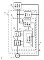
- FIG. 4 is a circuit of the noise suppression device 20 according to the first embodiment.
- the noise suppression device 20 (see the dotted line frame inside the figure) is a part of the noise filter 10 (see the dotted line frame outside the figure) for the purpose of reducing the common mode noise of the power conversion system. Or make up everything.
- the noise filter 10 is composed of the grounding capacitor 11 and the noise suppression device 20.
- the noise suppression device 20 is formed by a detection circuit 30 that detects a specific signal such as noise, and a waveform signal forming circuit 40 that forms a desired waveform signal based on the components detected from the detection circuit 30.
- a signal transmitter including an injection transformer 50 that transmits a waveform signal to a common mode, a state detector 60 that detects the operating state of the power converter 80 or the waveform signal forming circuit 40 itself, and a state detector 60 that detects the detected signal. It is composed of a gain adjuster 70 that adjusts the gain by a predetermined amount or a predetermined timing.
- FIG. 5 is a configuration example of the detection circuit 30 according to the first, second, third, fourth, and fifth embodiments, and shows a case where the detection circuit is configured by a common mode transformer.
- the detection transformer is inserted into the RST phase power line between the AC power supply 1 and the power conversion device 80 which is the controlled device, and the R phase winding 31, the S phase winding 32, and the T phase winding 33 are wound in the same phase. There is.
- the detection coil has a high inductance value only in the common mode and acts as a common mode choke coil.
- the common mode noise 4 passing through the detection transformer generates a noise detection signal 35 at both ends of the auxiliary winding 34. Both ends of the output of the auxiliary winding are connected to the waveform signal forming circuit 40.
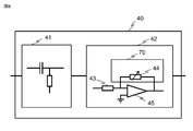
- FIG. 6 is an example of the waveform signal forming circuit according to the first, second, third, fourth, and fifth embodiments, and shows a case where the band limiting circuit 41 and the high frequency amplifier circuit 42 are configured.
- the band limiting circuit 41 attenuates low frequency components that are unnecessary for noise compensation by, for example, a passive filter composed of a resistor and a capacitor.
- the high-frequency amplifier circuit 42 forms an inverting or non-inverting amplifier circuit using, for example, an operational amplifier 45, and amplifies a signal whose unnecessary components are cut by the band limiting circuit 41 according to the ratio of the input resistor 43 and the feedback resistor 44. ..
- FIG. 7 is a configuration example of the signal transmitter according to the first, second, third, fourth, and fifth embodiments, and shows a case where the signal transmitter is configured by a common mode transformer.
- the injection transformer 50 is inserted into the RST phase power line between the detection circuit 30 and the power conversion device 80, and the R phase winding 51, the S phase winding 52, and the T phase winding 53 are wound in the same phase.
- a noise injection signal 55 is input to the auxiliary winding 54 so as to cancel the common mode noise (not shown) with respect to the common modes of the R-phase winding 51, the S-phase winding 52, and the T-phase winding 53.
- Common mode injection voltage 56 is input.
- the magnetic flux generated in the injection transformer 50 which is one of the signal transmitters, is the sum of the magnetic flux of the normal component generated by the product of the leakage inductance and the normal current and the magnetic flux of the common mode component generated by the active operation of the noise suppression device. be. Of these, the magnetic flux of the normal component rises, and the magnetic flux density in the core rises.
- the core magnetic design of the common mode transformer must be performed in consideration of the temporary overload or the rise of the normal component magnetic flux in the unbalanced state, and the core size is large. There was a problem that it became large and hindered miniaturization or cost reduction.
- the gain adjuster 70 can be used to reduce the gain by a predetermined time.
- the current state signal, the protection state signal, the specific state signal, and the operation state signal which will be described later, are collectively referred to as a state signal.
- FIG. 8 shows a configuration example of the gain adjuster 70 according to the first, second, third, fourth, and fifth embodiments, and shows a case where the gain adjuster 70 is configured by an up-down type digital potentiometer.
- the gain adjuster 70 is composed of a control IC 71 and a digital potentiometer 72.
- FIG. 9 shows an example of the operation of the configuration example of the gain adjuster 70 of FIG. 8 according to the first, second, third, fourth, and fifth embodiments.
- the state detection signal 60a which is one of the signals detected by the state detector 60, is represented by the low active signal DETECT (which is valid at the low level).
- the low active signal DETECT changes from high to low at timing t1 to detect an arbitrary state, and changes from low to high at timing t2 to end the detection of the arbitrary state.
- control IC 71 switches the chip select signal 73 of the digital potentiometer 72 from high (a state in which the resistance value cannot be switched) to low (a state in which the resistance value can be switched) at timing t1, and sets the up / down control input 74 to high (a state in which the resistance value can be switched). Switch from (up count) to low (down count).
- the logic of the three signals of the control IC 71 is all negative logic and is valid at a low level.
- the digital potentiometer 72 synchronizes with the falling edge of the increment control input 75 from high to low, and the resistance value 76 rises or falls with a predetermined resolution width according to the high state or low state of the up / down control input 74.
- the up / down control input 74 is low (down count)
- the resistance value 76 decreases, and the amplification gain of the high frequency amplifier circuit 42 decreases.
- the chip selector signal is delayed by a predetermined return time 77 to switch from low to high, and the lowered resistance value 76 is converted to the non-volatile value of the digital potentiometer.
- the operation of returning the resistance value 76 to the initial value is performed without recording in the memory. By this recovery operation, the temporarily increased amplification gain returns to the original value again after a predetermined recovery time as the overcurrent state is released.
- the current state signal 68b obtained from the power conversion device 80, which is a controlled device, is input to the state detector 60, and when the input value exceeds a predetermined threshold value, the gain is determined by using the gain adjuster 70. After the protection state is released, the amplification gain can be returned to the original value again with a predetermined recovery time.
- the noise compensation operation can be realized without causing design restrictions due to a temporary overload state.
- the injection transformer is provided by the waveform signal forming circuit.
- the current sensor output may be provided in the noise suppression device, and is not a direct current detection amount but an I / O signal (for example, an overcurrent state notification signal, a load sudden change notification signal, etc.) from the device. May be good.
- I / O signal for example, an overcurrent state notification signal, a load sudden change notification signal, etc.
- the band limiting circuit includes not only a high-pass filter that suppresses low frequencies, but also a low-pass filter that suppresses high frequencies, a notch filter that suppresses a specific band, a band-pass filter that passes a specific band, and the like within a range that does not deviate from the purpose of the present application. It can be configured freely. Further, the high-frequency amplifier circuit can be freely configured within a range that does not deviate from the gist of the present application, such as an inverting amplifier circuit using an operational amplifier and a non-inverting amplifier circuit.
- the configuration of the present embodiment may be not only a three-phase three-wire power conversion system but also a three-phase four-wire power conversion system.
- the gain adjuster is a combination of a control IC and a digital potentiometer having a communication interface, a combination of an analog network and an up-down digital potentiometer, a resistance short circuit using a semiconductor switch, or a load switch between different analog control networks. It can be freely configured within a range that does not deviate from the gist of the present application, such as switching the resistance and capacitor capacitance value by switching between the two, and switching the resistance value by an electronic resistance whose resistance value can be changed.
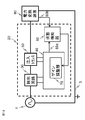
- FIG. 10 is a circuit of the noise suppression device 20 according to the second embodiment.
- the difference between the noise suppression device 20 according to the second embodiment and the noise suppression device 20 according to the first embodiment is that the signal input to the state detector 60 is a protection state signal 65 instead of the current state signal 68a. It is a point.
- the injection current becomes an overcurrent in the waveform signal forming circuit 40 for some reason (for example, when the common mode transformer of the signal transmitter which is a noise injection means causes instantaneous magnetic saturation due to the intrusion of external noise such as a lightning surge). ), It is necessary to stop the operation of the device in order to protect the circuit components of the waveform signal forming circuit 40.
- this operation is realized by selecting a component with a built-in protection circuit as the circuit component of the waveform signal forming circuit 40, the component with a built-in protection circuit is generally expensive and there are restrictions on the lineup, so there are design restrictions. There was a problem that caused.
- FIG. 11 is a configuration example of the state detector 60 according to the first, second, third, fourth, and fifth embodiments, and shows a case where the state detector 60 is configured by a single injection current overcurrent detection circuit.
- the shunt resistance 61 inserted in series with respect to the output of the waveform signal forming circuit 40 and the input of the injection transformer 50, which is one of the signal transmitters, and both ends of the shunt resistance in proportion to the injection current value. It is composed of a comparator 62 that compares the generated injection current detection voltage with a predetermined threshold, and a threshold creation circuit 63 that supplies a predetermined threshold to the comparator 62, and the output of the comparator 62 becomes an overcurrent detection signal of the injection current.
- the state detector 60 receives a specific state signal 66 (for example, an overload state detection signal indicating that the device is in an overload state) indicating a specific state from the power conversion device 80 which is a controlled device.
- a specific state signal 66 for example, an overload state detection signal indicating that the device is in an overload state
- An interface circuit that receives from the O port may be added.
- an interface circuit for receiving an overheat state detection signal from the thermistor provided in the cooling fin for cooling the heat generating component of the injection circuit may be added.
- the protection state signal 65 obtained by an appropriate means such as an inexpensive shunt resistor 61 provided in the waveform signal forming circuit 40 is input to the state detector 60, and the input value is a predetermined threshold value.
- the gain adjuster 70 can be used to reduce the gain for a predetermined time, and after the protection state is released, the amplification gain can be returned to the original value again with a predetermined recovery time.
- the magnetic flux of the common mode component among the core magnetic fluxes indicated by the sum of the common mode component and the normal mode component is temporarily used.
- the core size can be reduced, and the noise suppression device can be reduced in size and cost.
- Embodiment 3 is a modification of the second embodiment shown in FIG.
- the difference between the noise suppression device 20 according to the third embodiment and the noise suppression device 20 according to the second embodiment is that the operation of the gain adjuster 70 after the detection of the protection state signal is performed after a predetermined recovery time has elapsed. The point is that the amplification gain is gradually lowered to a minute value without immediately returning to the original amplification gain, and then raised again to reach the recovery.
- a core having a high magnetic permeability for example, a nanocrystalline magnetic material having a high magnetic permeability such as Finemet, has a problem because the residual magnetic flux is larger than that of a general ferrite material.
- the compensation gain of the waveform signal forming circuit 40 is returned to the value before the protection operation is activated, and the amplification gain is gradually reduced to a minute value. As a result, the residual magnetic flux can be demagnetized.
- the noise suppression device 20 starts output again after being cut off by the protection operation, the compensation gain is gradually increased over a predetermined time to soft-start the waveform signal forming circuit 40 and consume the circuit. It is possible to suppress current overshoot and reduce the circuit power supply capacity.
- FIG. 12 is a circuit of the noise suppression device according to the fourth embodiment.
- the difference between the noise suppression device 20 according to the fourth embodiment and the noise suppression device 20 according to the second embodiment is that the signal input to the state detector 60 is an operating state signal 69a instead of the protection state signal 65. It is a point.
- the power conversion device 80 has a plurality of operation modes
- the switching pattern of the semiconductor switch changes, so that the amplitude of noise and the generated frequency generally change, and the noise standard.
- the amount of attenuation required for the noise suppression device 20 or the frequency characteristic changes in order to satisfy the above conditions.
- the operating state signal 69b obtained from the power converter 80 is input to the state detector 60, and the gain adjuster 70 is used to set the amplification gain of the waveform signal forming circuit 40 to the value of the operating state signal 69b. It can be changed to a predetermined amplification gain according to the situation.
- the noise compensation operation can be realized without causing the design constraint of the noise suppression device 20 depending on the operation mode. can.
- the amplification gain of the waveform signal forming circuit 40 is operated according to each noise amplitude and generation frequency pattern.
- the core size of the waveform signal forming circuit 40 and the injection transformer 50 which is one of the signal transmitters, can be reduced, and the noise suppression device 20 can be reduced in size. The noise suppression effect can be maximized while reducing the circuit component rating and circuit power supply capacity.
- Embodiment 5 is a modification of the first, second, third, and fourth embodiments.
- the protection operation of the waveform signal forming circuit 40 according to the first embodiment typically, when the amount of noise or the frequency band of noise changes due to heat generation of the device or a transformer, it is optimal. As the compensation gain changes, the protection operation may continue to work.
- the gain adjuster 70 determines only the predetermined width. Permanently reduce the amplification gain.
- the chip select signal 73 is started up while the increment control input 75 is not in the low state but in the high state.
- the amplification gain is permanently reduced by a predetermined width.
- the optimum amplification gain is considered to be at a higher value, and the gain adjuster can permanently increase the amplification gain by a predetermined width. can. As a result, a compact, low-cost, and robust noise suppression device can be realized.
- FIG. 13 shows an example of the hardware 92 related to the signal processing of the noise suppression device of the present application.
- the hardware 92 related to the signal processing of the present apparatus includes a processor 93 and a storage device 94.
- the storage device includes a volatile storage device such as a random access memory and a non-volatile auxiliary storage device such as a flash memory. Further, an auxiliary storage device of a hard disk may be provided instead of the flash memory.
- the processor 93 executes the program input from the storage device 94.
- the program is input from the auxiliary storage device to the processor 93 via the volatile storage device.
- the processor 93 may output data such as a calculation result to the volatile storage device of the storage device 94, or may store the data in the auxiliary storage device via the volatile storage device.
Landscapes
- Engineering & Computer Science (AREA)
- Power Engineering (AREA)
- Inverter Devices (AREA)
- Power Conversion In General (AREA)
Abstract
Un dispositif de suppression de bruit (20) disposé entre une alimentation en courant alternatif et un dispositif à commander et émettant un signal au dispositif à commander comprend : un circuit de détection (30) destiné à détecter un signal spécifique ; un circuit de formation de signal de forme d'onde (40) destiné à former un signal de forme d'onde prédéterminé à partir du signal spécifique détecté par le circuit de détection (30) ; un émetteur de signal (50) destiné à émettre le signal de forme d'onde formé par le circuit de formation de signal de forme d'onde (40) vers le dispositif à commander ; un détecteur d'état (60) destiné à détecter un signal d'état indiquant l'état du dispositif à commander ou du circuit de formation de signal de forme d'onde (40) ; et un dispositif de réglage de gain (70) intégré dans le circuit de formation de signal de forme d'onde (40) et réglant le gain du signal de forme d'onde en fonction de l'un quelconque des signaux d'état détectés par le détecteur d'état (60). Le signal de forme d'onde ajusté par le dispositif de réglage de gain (70) est émis vers le dispositif à commander.
Priority Applications (3)
| Application Number | Priority Date | Filing Date | Title |
|---|---|---|---|
| JP2021518024A JP6906731B1 (ja) | 2020-02-17 | 2020-02-17 | ノイズ抑制装置 |
| PCT/JP2020/005972 WO2021166018A1 (fr) | 2020-02-17 | 2020-02-17 | Dispositif de suppression de bruit |
| DE112020006741.6T DE112020006741T5 (de) | 2020-02-17 | 2020-02-17 | Störungsunterdrückungseinrichtung |
Applications Claiming Priority (1)
| Application Number | Priority Date | Filing Date | Title |
|---|---|---|---|
| PCT/JP2020/005972 WO2021166018A1 (fr) | 2020-02-17 | 2020-02-17 | Dispositif de suppression de bruit |
Publications (1)
| Publication Number | Publication Date |
|---|---|
| WO2021166018A1 true WO2021166018A1 (fr) | 2021-08-26 |
Family
ID=76918289
Family Applications (1)
| Application Number | Title | Priority Date | Filing Date |
|---|---|---|---|
| PCT/JP2020/005972 WO2021166018A1 (fr) | 2020-02-17 | 2020-02-17 | Dispositif de suppression de bruit |
Country Status (3)
| Country | Link |
|---|---|
| JP (1) | JP6906731B1 (fr) |
| DE (1) | DE112020006741T5 (fr) |
| WO (1) | WO2021166018A1 (fr) |
Cited By (3)
| Publication number | Priority date | Publication date | Assignee | Title |
|---|---|---|---|---|
| WO2023054660A1 (fr) * | 2021-09-30 | 2023-04-06 | ダイキン工業株式会社 | Circuit de réduction de bruit, dispositif de conversion de puissance et dispositif de réfrigération |
| WO2023105687A1 (fr) * | 2021-12-08 | 2023-06-15 | 三菱電機株式会社 | Filtre de bruit |
| WO2024075267A1 (fr) * | 2022-10-07 | 2024-04-11 | 三菱電機株式会社 | Filtre de bruit, système de conversion de puissance et système de gestion |
Citations (5)
| Publication number | Priority date | Publication date | Assignee | Title |
|---|---|---|---|---|
| JP2004357421A (ja) * | 2003-05-29 | 2004-12-16 | Matsushita Electric Ind Co Ltd | ノイズ抑圧装置 |
| JP2004357447A (ja) * | 2003-05-30 | 2004-12-16 | Meidensha Corp | 電力変換装置のノイズ低減装置 |
| JP2005204395A (ja) * | 2004-01-14 | 2005-07-28 | Sanken Electric Co Ltd | ノイズ低減装置及び電力変換装置 |
| JP2010057268A (ja) * | 2008-08-28 | 2010-03-11 | Fuji Electric Systems Co Ltd | 伝導性ノイズフィルタ |
| WO2011125944A1 (fr) * | 2010-04-05 | 2011-10-13 | 三菱電機株式会社 | Dispositif de réduction de courant de fuite |
-
2020
- 2020-02-17 JP JP2021518024A patent/JP6906731B1/ja active Active
- 2020-02-17 DE DE112020006741.6T patent/DE112020006741T5/de active Pending
- 2020-02-17 WO PCT/JP2020/005972 patent/WO2021166018A1/fr active Application Filing
Patent Citations (5)
| Publication number | Priority date | Publication date | Assignee | Title |
|---|---|---|---|---|
| JP2004357421A (ja) * | 2003-05-29 | 2004-12-16 | Matsushita Electric Ind Co Ltd | ノイズ抑圧装置 |
| JP2004357447A (ja) * | 2003-05-30 | 2004-12-16 | Meidensha Corp | 電力変換装置のノイズ低減装置 |
| JP2005204395A (ja) * | 2004-01-14 | 2005-07-28 | Sanken Electric Co Ltd | ノイズ低減装置及び電力変換装置 |
| JP2010057268A (ja) * | 2008-08-28 | 2010-03-11 | Fuji Electric Systems Co Ltd | 伝導性ノイズフィルタ |
| WO2011125944A1 (fr) * | 2010-04-05 | 2011-10-13 | 三菱電機株式会社 | Dispositif de réduction de courant de fuite |
Cited By (5)
| Publication number | Priority date | Publication date | Assignee | Title |
|---|---|---|---|---|
| WO2023054660A1 (fr) * | 2021-09-30 | 2023-04-06 | ダイキン工業株式会社 | Circuit de réduction de bruit, dispositif de conversion de puissance et dispositif de réfrigération |
| JP2023051443A (ja) * | 2021-09-30 | 2023-04-11 | ダイキン工業株式会社 | ノイズ低減回路、電力変換装置及び冷凍装置 |
| JP7288206B2 (ja) | 2021-09-30 | 2023-06-07 | ダイキン工業株式会社 | ノイズ低減回路、電力変換装置及び冷凍装置 |
| WO2023105687A1 (fr) * | 2021-12-08 | 2023-06-15 | 三菱電機株式会社 | Filtre de bruit |
| WO2024075267A1 (fr) * | 2022-10-07 | 2024-04-11 | 三菱電機株式会社 | Filtre de bruit, système de conversion de puissance et système de gestion |
Also Published As
| Publication number | Publication date |
|---|---|
| DE112020006741T5 (de) | 2022-12-22 |
| JP6906731B1 (ja) | 2021-07-21 |
| JPWO2021166018A1 (fr) | 2021-08-26 |
Similar Documents
| Publication | Publication Date | Title |
|---|---|---|
| WO2021166018A1 (fr) | Dispositif de suppression de bruit | |
| US7755869B2 (en) | Ground protection device for electronic stability and personal safety | |
| EP1289108B1 (fr) | Appareil pour réduire le bruit de courant dans les convertisseurs de puissance | |
| CN112262523A (zh) | 一种在电源线上无附加元件的隔离型有源emi滤波器 | |
| US20030197989A1 (en) | Method and apparatus for high impedance grounding of medium voltage AC drives | |
| US8354910B2 (en) | Coil block and electronic device using the same | |
| CN110383657B (zh) | 有源补偿电路和系统 | |
| KR20020038789A (ko) | 비-포화 자기 요소 전력 컨버터 및 서지 방지 | |
| EP1658669A1 (fr) | Dispositif destine a la reduction du courant de bruit dans des convertisseurs de puissance | |
| US6288917B1 (en) | Three stage power conditioning circuit | |
| JP2003087973A (ja) | アクティブフィルタ | |
| US7446436B2 (en) | Waveform correction filters | |
| CN114252741A (zh) | 具有宽带传感器的电弧故障检测装置 | |
| US3646397A (en) | Amplifier protection circuit responsive to temperature and overcurrent | |
| US5313358A (en) | Multiphase common mode transient suppressor | |
| JP2001244770A (ja) | ノイズフィルター | |
| CN111025075B (zh) | 一种电磁骚扰测试系统 | |
| CA1099341A (fr) | Circuit permettant de detecter les pertes a la terre dans un convertisseur | |
| CA1203284A (fr) | Detecteur de courants hybride | |
| JP4715537B2 (ja) | 漏電遮断器 | |
| KR102551607B1 (ko) | 누전 차단기 | |
| CA1236525A (fr) | Coupe-circuit a semiconducteur du type limiteur pour courant alternatif | |
| JP2002165454A (ja) | 交流電圧調整装置 | |
| JP2015103939A (ja) | 半導体装置 | |
| JP3270214B2 (ja) | 直交磁心限流器 |
Legal Events
| Date | Code | Title | Description |
|---|---|---|---|
| ENP | Entry into the national phase |
Ref document number: 2021518024 Country of ref document: JP Kind code of ref document: A |
|
| 121 | Ep: the epo has been informed by wipo that ep was designated in this application |
Ref document number: 20919961 Country of ref document: EP Kind code of ref document: A1 |
|
| 122 | Ep: pct application non-entry in european phase |
Ref document number: 20919961 Country of ref document: EP Kind code of ref document: A1 |