WO2024075236A1 - 電源装置 - Google Patents
電源装置 Download PDFInfo
- Publication number
- WO2024075236A1 WO2024075236A1 PCT/JP2022/037404 JP2022037404W WO2024075236A1 WO 2024075236 A1 WO2024075236 A1 WO 2024075236A1 JP 2022037404 W JP2022037404 W JP 2022037404W WO 2024075236 A1 WO2024075236 A1 WO 2024075236A1
- Authority
- WO
- WIPO (PCT)
- Prior art keywords
- circuit
- signal
- control signal
- abnormality
- semiconductor switch
- Prior art date
- Legal status (The legal status is an assumption and is not a legal conclusion. Google has not performed a legal analysis and makes no representation as to the accuracy of the status listed.)
- Ceased
Links
Images



Classifications
-
- H—ELECTRICITY
- H02—GENERATION; CONVERSION OR DISTRIBUTION OF ELECTRIC POWER
- H02H—EMERGENCY PROTECTIVE CIRCUIT ARRANGEMENTS
- H02H7/00—Emergency protective circuit arrangements specially adapted for specific types of electric machines or apparatus or for sectionalised protection of cable or line systems, and effecting automatic switching in the event of an undesired change from normal working conditions
- H02H7/20—Emergency protective circuit arrangements specially adapted for specific types of electric machines or apparatus or for sectionalised protection of cable or line systems, and effecting automatic switching in the event of an undesired change from normal working conditions for electronic equipment
- H02H7/205—Emergency protective circuit arrangements specially adapted for specific types of electric machines or apparatus or for sectionalised protection of cable or line systems, and effecting automatic switching in the event of an undesired change from normal working conditions for electronic equipment for controlled semi-conductors which are not included in a specific circuit arrangement
-
- H—ELECTRICITY
- H02—GENERATION; CONVERSION OR DISTRIBUTION OF ELECTRIC POWER
- H02M—APPARATUS FOR CONVERSION BETWEEN AC AND AC, BETWEEN AC AND DC, OR BETWEEN DC AND DC, AND FOR USE WITH MAINS OR SIMILAR POWER SUPPLY SYSTEMS; CONVERSION OF DC OR AC INPUT POWER INTO SURGE OUTPUT POWER; CONTROL OR REGULATION THEREOF
- H02M1/00—Details of apparatus for conversion
- H02M1/08—Circuits specially adapted for the generation of control voltages for semiconductor devices incorporated in static converters
- H02M1/088—Circuits specially adapted for the generation of control voltages for semiconductor devices incorporated in static converters for the simultaneous control of series or parallel connected semiconductor devices
-
- H—ELECTRICITY
- H02—GENERATION; CONVERSION OR DISTRIBUTION OF ELECTRIC POWER
- H02H—EMERGENCY PROTECTIVE CIRCUIT ARRANGEMENTS
- H02H3/00—Emergency protective circuit arrangements for automatic disconnection directly responsive to an undesired change from normal electric working condition with or without subsequent reconnection ; integrated protection
- H02H3/02—Details
- H02H3/05—Details with means for increasing reliability, e.g. redundancy arrangements
-
- H—ELECTRICITY
- H02—GENERATION; CONVERSION OR DISTRIBUTION OF ELECTRIC POWER
- H02H—EMERGENCY PROTECTIVE CIRCUIT ARRANGEMENTS
- H02H7/00—Emergency protective circuit arrangements specially adapted for specific types of electric machines or apparatus or for sectionalised protection of cable or line systems, and effecting automatic switching in the event of an undesired change from normal working conditions
- H02H7/10—Emergency protective circuit arrangements specially adapted for specific types of electric machines or apparatus or for sectionalised protection of cable or line systems, and effecting automatic switching in the event of an undesired change from normal working conditions for converters; for rectifiers
- H02H7/12—Emergency protective circuit arrangements specially adapted for specific types of electric machines or apparatus or for sectionalised protection of cable or line systems, and effecting automatic switching in the event of an undesired change from normal working conditions for converters; for rectifiers for static converters or rectifiers
- H02H7/1203—Circuits independent of the type of conversion
-
- H—ELECTRICITY
- H02—GENERATION; CONVERSION OR DISTRIBUTION OF ELECTRIC POWER
- H02J—ELECTRIC POWER NETWORKS; CIRCUIT ARRANGEMENTS OR SYSTEMS FOR SUPPLYING OR DISTRIBUTING ELECTRIC POWER; SYSTEMS FOR STORING ELECTRIC ENERGY
- H02J9/00—Circuit arrangements for emergency or stand-by power supply, e.g. for emergency lighting
- H02J9/04—Circuit arrangements for emergency or stand-by power supply, e.g. for emergency lighting in which the distribution system is disconnected from the normal source and connected to a standby source
- H02J9/06—Circuit arrangements for emergency or stand-by power supply, e.g. for emergency lighting in which the distribution system is disconnected from the normal source and connected to a standby source with automatic change-over, e.g. UPS systems
-
- H—ELECTRICITY
- H02—GENERATION; CONVERSION OR DISTRIBUTION OF ELECTRIC POWER
- H02M—APPARATUS FOR CONVERSION BETWEEN AC AND AC, BETWEEN AC AND DC, OR BETWEEN DC AND DC, AND FOR USE WITH MAINS OR SIMILAR POWER SUPPLY SYSTEMS; CONVERSION OF DC OR AC INPUT POWER INTO SURGE OUTPUT POWER; CONTROL OR REGULATION THEREOF
- H02M1/00—Details of apparatus for conversion
- H02M1/32—Means for protecting converters other than automatic disconnection
-
- H—ELECTRICITY
- H02—GENERATION; CONVERSION OR DISTRIBUTION OF ELECTRIC POWER
- H02M—APPARATUS FOR CONVERSION BETWEEN AC AND AC, BETWEEN AC AND DC, OR BETWEEN DC AND DC, AND FOR USE WITH MAINS OR SIMILAR POWER SUPPLY SYSTEMS; CONVERSION OF DC OR AC INPUT POWER INTO SURGE OUTPUT POWER; CONTROL OR REGULATION THEREOF
- H02M7/00—Conversion of AC power input into DC power output; Conversion of DC power input into AC power output
- H02M7/66—Conversion of AC power input into DC power output; Conversion of DC power input into AC power output with possibility of reversal
- H02M7/68—Conversion of AC power input into DC power output; Conversion of DC power input into AC power output with possibility of reversal by static converters
- H02M7/72—Conversion of AC power input into DC power output; Conversion of DC power input into AC power output with possibility of reversal by static converters using discharge tubes with control electrode or semiconductor devices with control electrode
- H02M7/79—Conversion of AC power input into DC power output; Conversion of DC power input into AC power output with possibility of reversal by static converters using discharge tubes with control electrode or semiconductor devices with control electrode using devices of a triode or transistor type requiring continuous application of a control signal
- H02M7/797—Conversion of AC power input into DC power output; Conversion of DC power input into AC power output with possibility of reversal by static converters using discharge tubes with control electrode or semiconductor devices with control electrode using devices of a triode or transistor type requiring continuous application of a control signal using semiconductor devices only
-
- H—ELECTRICITY
- H03—ELECTRONIC CIRCUITRY
- H03K—PULSE TECHNIQUE
- H03K17/00—Electronic switching or gating, i.e. not by contact-making and –breaking
- H03K17/08—Modifications for protecting switching circuit against overcurrent or overvoltage
-
- H—ELECTRICITY
- H03—ELECTRONIC CIRCUITRY
- H03K—PULSE TECHNIQUE
- H03K17/00—Electronic switching or gating, i.e. not by contact-making and –breaking
- H03K17/18—Modifications for indicating state of switch
-
- H—ELECTRICITY
- H02—GENERATION; CONVERSION OR DISTRIBUTION OF ELECTRIC POWER
- H02M—APPARATUS FOR CONVERSION BETWEEN AC AND AC, BETWEEN AC AND DC, OR BETWEEN DC AND DC, AND FOR USE WITH MAINS OR SIMILAR POWER SUPPLY SYSTEMS; CONVERSION OF DC OR AC INPUT POWER INTO SURGE OUTPUT POWER; CONTROL OR REGULATION THEREOF
- H02M1/00—Details of apparatus for conversion
- H02M1/08—Circuits specially adapted for the generation of control voltages for semiconductor devices incorporated in static converters
- H02M1/088—Circuits specially adapted for the generation of control voltages for semiconductor devices incorporated in static converters for the simultaneous control of series or parallel connected semiconductor devices
- H02M1/092—Circuits specially adapted for the generation of control voltages for semiconductor devices incorporated in static converters for the simultaneous control of series or parallel connected semiconductor devices the control signals being transmitted optically
Definitions
- This disclosure relates to a power supply device, and in particular to a power supply device having multiple semiconductor switches connected in series.
- Patent Document 1 discloses a semiconductor switch control device configured to detect abnormalities in a semiconductor switch used in a power conversion device.
- the control device includes a control circuit that provides a drive signal to a semiconductor switch element, an isolation circuit that optically isolates the drive signal and transmits it to a high-voltage circuit, and a drive circuit that generates a gate voltage for the semiconductor switch element based on the drive signal.
- the semiconductor switch element is turned on or off in response to the drive signal.
- the control device further includes a gate voltage detection circuit that determines whether the semiconductor switch element is in an on or off state based on the output gate voltage of the drive circuit, a signal isolation circuit that optically isolates the gate voltage state signal of the semiconductor switch element and transmits it to the low-voltage circuit, and an abnormality detection circuit that detects an abnormality in the semiconductor switch element based on the transmitted gate voltage state signal.
- the abnormality detection circuit is configured to feed back an abnormality signal to the control circuit to shut off the semiconductor switch element.
- control device When the above-mentioned control device is applied to a power supply device having multiple semiconductor switches connected in series to detect abnormalities in each semiconductor switch, it becomes necessary to install wiring for connecting a control circuit, an isolation circuit, and a drive circuit for each semiconductor switch. It also becomes necessary to install wiring for connecting a gate voltage detection circuit, a signal isolation circuit, and an abnormality detection circuit for each semiconductor switch. This raises concerns that the power supply device configuration may become complicated.
- the abnormality detection circuit is configured to determine whether the semiconductor switch element is normal or abnormal by comparing the drive signal with the gate voltage state signal transmitted from the gate voltage detection circuit. Therefore, when an abnormality in the semiconductor switch element is detected, it is not possible to determine whether an abnormality has occurred in the drive circuit or in the insulation circuit that transmits the drive signal and gate state signal. Therefore, when the above control device is applied to a power supply device equipped with multiple semiconductor switches, there is a concern that it may become difficult to identify the type of abnormality and where it has occurred.
- This disclosure has been made to solve the problems described above, and the purpose of this disclosure is to make it possible to identify the content and location of an abnormality in a power supply device equipped with multiple semiconductor switches connected in series, without complicating the device configuration.
- a power supply device includes first to n-th semiconductor switches connected in series between first and second terminals, first to n-th drive circuits, an interface circuit, and first and second communication lines.
- the first to n-th drive circuits are provided corresponding to the first to n-th semiconductor switches, respectively, and drive the corresponding semiconductor switches in response to a control signal.
- the interface circuit transmits and receives signals to and from the first to n-th drive circuits.
- the first and second communication lines connect the interface circuit and the first to n-th drive circuits in series.
- the first communication line is configured to transmit control signals sequentially from the interface circuit to the n-th drive circuit via the first drive circuit.
- the second communication line is configured to transmit state detection signals indicating the operating state of the semiconductor switches sequentially from the n-th drive circuit to the interface circuit via the first drive circuit.
- the i-th drive circuit includes a driver that drives the i-th semiconductor switch in response to a control signal received from the (i-1)-th drive circuit, an abnormality detection circuit for detecting an abnormality in the i-th semiconductor switch, and first and second notification members.
- the abnormality detection circuit detects an abnormality in the i-th semiconductor switch based on the control signal and the operating state of the i-th semiconductor switch, and notifies the detection result using the first notification member.
- the abnormality detection circuit generates a state detection signal indicating the operating state of the i-th to n-th semiconductor switches based on the operating state of the i-th semiconductor switch and a state detection signal indicating the operating states of the (i+1)-th to n-th semiconductor switches received from the (i+1)-th drive circuit.
- the abnormality detection circuit detects a mismatch between the control signal and the operating states of the i-th to n-th semiconductor switches based on the control signal and the generated state detection signal, and notifies the detection result using the second notification member.
- FIG. 1 is a diagram showing a schematic configuration of a power supply device according to an embodiment
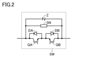
- FIG. 4 is a circuit diagram showing another example of the configuration of the semiconductor switch shown in FIG. 2 is a circuit block diagram showing a configuration of a portion of a control device that is related to control of a switch circuit.
- FIG. FIG. 2 is a circuit block diagram showing an example of the configuration of a gate driver.
- 5 is a circuit diagram showing a configuration example of an abnormality detection circuit shown in FIG. 4.
- FIG. 11 is a diagram for explaining a first example of an abnormality detection operation of a gate driver.
- FIG. 11 is a diagram for explaining a second example of the abnormality detection operation of the gate driver.
- FIG. 13 is a diagram for explaining a third example of an abnormality detection operation of a gate driver.
- FIG. 1 is a diagram showing a schematic configuration of a power supply device according to a comparative example.
- FIG. 1 is a diagram showing a schematic configuration of a power supply device according to an embodiment.
- the power supply device 10 is connected between an AC power source 1 and a load 2, and is configured to receive AC power from the AC power source 1 and supply AC power to the load 2.
- the power supply device 10 can be used as a multiple power compensator, which is a device for supplying stable AC power to the load 2 without momentary interruption when a power outage or momentary voltage drop occurs in the AC power source 1, for example.
- the AC power source 1 is typically a commercial AC power source, and supplies AC power of a commercial frequency to the power supply device 10.
- the load 2 is driven by the AC power of the commercial frequency supplied from the power supply device 10. Note that while FIG. 1 only shows the portion related to one phase of AC power, the power supply device 10 may receive three-phase AC power and output three-phase AC power.
- the power supply device 10 includes an input terminal T1, an output terminal T2, a DC terminal T3, a switch circuit 14, a bidirectional converter 16, voltage detectors 18 and 20, and a control device 30.
- the input terminal T1 is electrically connected to the AC power source 1 and receives the commercial frequency AC voltage V1 supplied from the AC power source 1.
- the input terminal T1 corresponds to one embodiment of the "first terminal.”
- the output terminal T2 is connected to the load 2.
- the load 2 is driven by the AC voltage VO supplied from the output terminal T2.
- the output terminal T2 corresponds to one embodiment of the "second terminal.”
- the DC terminal T3 is connected to the battery 3.
- the battery 3 corresponds to one embodiment of a "power storage device” that stores DC power. Instead of the battery 3, an electric double layer capacitor may be connected to the DC terminal T3 as a power storage device.
- the instantaneous value of the DC voltage VB (terminal voltage of the battery 3) at the DC terminal T3 is detected by the control device 30.
- the switch circuit 14 has an input node 14a and an output node 14b, and n semiconductor switches SW1 to SWn (n is an integer equal to or greater than 2).
- the input node 14a is connected to the input terminal T1
- the output node 14b is connected to the output terminal T2.
- n 4.
- the number n of semiconductor switches is not limited to 4.
- the semiconductor switches SW1 to SWn are controlled to be on and off by gate signals G1 to Gn, respectively, input from the control device 30.
- gate signals G1 to Gn are also be referred to simply as "gate signals G.”
- the semiconductor switch SWi (i is an integer between 1 and n) has an IGBT (Insulated Gate Bipolar Transistor) Qi, a diode Di connected in anti-parallel to the IGBT Qi, a snubber circuit SNi, and a varistor Zi.
- the collector of the IGBT Qi is electrically connected to the input node 14a, and the emitter is electrically connected to the output node 14b.
- the IGBT Qi is turned on (conductive) by a gate signal Gi at an H (logical high) level, and turned off (cut off) by a gate signal Gi at an L (logical low) level.
- the diode Di is connected with the forward direction being from the output node 14b toward the input node 14a.
- the semiconductor switch SWi is not limited to an IGBT, and any self-extinguishing semiconductor switching element can be used.
- Snubber circuit SNi is connected in parallel to IGBTQi and protects IGBTQi from surge voltages.
- Snubber circuit SNi has, for example, a resistor element and a capacitor connected in series between the collector and emitter of IGBTQi. If IGBTQi is suddenly turned off while a current is flowing through it, a surge voltage will occur between the collector and emitter of IGBTQi due to its self-inductance. Snubber circuit SNi protects IGBTQi by suppressing such surge voltages.
- the varistor Zi is connected in parallel to the IGBT Qi.
- the varistor Zi is a resistor whose resistance value is voltage dependent.
- the varistor Zi is, for example, a zinc oxide nonlinear resistor (ZnR).
- ZnR zinc oxide nonlinear resistor
- the resistance value of the varistor Zi changes according to the voltage between its terminals, and drops suddenly when the voltage between the terminals exceeds a threshold voltage. Therefore, the collector-emitter voltage of the IGBT Qi is prevented from exceeding the threshold voltage, and as a result, the IGBT Qi can be prevented from being destroyed by a surge voltage.
- IGBTs Q1 to Qn when IGBTs Q1 to Qn are referred to collectively, they will be referred to simply as "IGBTQ”.
- snubber circuits SN1 to SNn When snubber circuits SN1 to SNn are referred to collectively, they will be referred to simply as “snubber circuit SN”.
- varistors Z1 to Zn When varistors Z1 to Zn are referred to collectively, they will be referred to simply as "varistor Z".
- the semiconductor switch SW is not limited to the configuration shown in FIG. 1, and may be configured as shown in FIG. 2, for example.
- the semiconductor switch SW has IGBTs QA and QB connected in anti-series, diodes DA and DB connected in anti-parallel to IGBTs QA and QB, respectively, a snubber circuit SN, and a varistor Z.
- the collector of IGBT QA is electrically connected to the input node 14a, and the emitter is connected to the emitter of IGBT QB.
- the collector of IGBT QB is electrically connected to the output node 14b.
- the diode DA is connected with the forward direction being from the output node 14b toward the input node 14a.
- the diode DB is connected with the forward direction being from the input node 14a toward the output node 14b.
- the snubber circuit SN and the varistor Z are connected in parallel to the series circuit of IGBTs QA and QB.
- the bidirectional converter 16 is connected between the output node 14b of the switch circuit 14 and the DC terminal T3.
- the bidirectional converter 16 is configured to perform bidirectional power conversion between the AC power output to the output node 14b and the DC power stored in the battery 3.
- the bidirectional converter 16 converts the AC power supplied from the AC power source 1 via the switch circuit 14 into DC power and stores the DC power in the battery 3.
- the bidirectional converter 16 converts the DC power of the battery 3 into AC power of the commercial frequency and supplies the AC power to the load 2.
- the bidirectional converter 16 has multiple semiconductor switching elements (not shown). The multiple semiconductor switching elements are controlled to be turned on and off by a control signal generated by the control device 30.
- the bidirectional converter 16 can perform bidirectional power conversion between the AC power output to the output node 14b and the DC power input/output to the DC terminal T3 by turning the multiple semiconductor switching elements on and off in response to the control signal.
- the voltage detector 18 detects the instantaneous value of the AC voltage VI supplied from the AC power source 1 to the input terminal T1, and provides a signal indicating the detected value to the control device 30.
- the control device 30 determines whether the AC power source 1 is normal or not based on the instantaneous value of the AC voltage VI. For example, if the AC voltage VI is higher than a predetermined lower limit voltage, the control device 30 determines that the AC power source 1 is normal. If the AC voltage VI falls below the lower limit voltage, the control device 30 determines that the AC power source 1 is abnormal.
- the voltage detector 20 detects the instantaneous value of the AC voltage VO appearing at the output terminal T20 and provides a signal indicating the detected value to the control device 30.
- the semiconductor switch SWi provides the control device 30 with a signal Vgei that indicates the magnitude of the gate-emitter voltage Vge of the IGBTQi.
- the gate-emitter voltage Vge is also referred to as the "gate voltage Vge.”
- the gate voltage Vge is a voltage higher than the threshold voltage Vth of the IGBTQ when the IGBTQ is in the on state, and a voltage lower than the threshold voltage Vth when the IGBTQ is in the off state. Therefore, it is possible to determine whether the IGBTQ is in the on state or the off state from the magnitude of the gate voltage Vge.
- the control device 30 controls the operation of the switch circuit 14 and the bidirectional converter 16 using commands from a higher-level controller (not shown), signals input from the voltage detectors 18 and 20, and signals input from the switch circuit 14.
- the control device 30 can be configured, for example, with a microcomputer.
- the control device 30 has a CPU (Central Processing Unit) and memory (not shown), and can execute the control operations described below through software processing in which the CPU executes a program stored in the memory.
- some or all of the control operations can be realized by hardware processing using built-in dedicated electronic circuits instead of software processing.
- the control device 30 When the AC power supply 1 is normal, the control device 30 provides H-level gate signals G1 to Gn to the semiconductor switches SW1 to SWn of the switch circuit 14, respectively. When the semiconductor switches SW1 to SWn are turned on, AC power is supplied from the AC power supply 1 to the load 2 via the switch circuit 14, and the load 2 is driven. In addition, AC power is supplied from the AC power supply 1 to the bidirectional converter 16 via the switch circuit 14, and the AC power is converted to DC power and stored in the battery 3. At this time, the control device 30 controls the bidirectional converter 16 so that the terminal voltage VB of the battery 3 becomes the reference voltage VBr.
- the control device 30 When an abnormality occurs in the AC power supply 1 (when the AC power supply 1 experiences a power outage or momentary voltage drop), the control device 30 provides L-level gate signals G1 to Gn to the semiconductor switches SW1 to SWn, respectively.
- the semiconductor switches SW1 to SWn are instantly turned off, and the DC power of the battery 3 is converted to AC power by the bidirectional converter 16 and supplied to the load 2. Therefore, even if an abnormality occurs in the AC power supply 1, the operation of the load 2 can be continued while DC power is stored in the battery 3.
- the control device 30 controls the bidirectional converter 16 based on the AC voltage VO detected by the voltage detector 20 so that the AC voltage VO becomes the reference voltage VOr.
- the control device 30 stops the operation of the bidirectional converter 16.
- the switch circuit 14 will not be able to operate normally. This will make it difficult for the power supply device 10 to stably supply power to the load 2.
- the semiconductor switch SW in question will be maintained in the on state during an abnormality in the AC power supply 1, and the voltage difference between the input node 14a and the output node 14b will be concentrated across the terminals of the remaining semiconductor switches SW that are in the off state, raising concerns that the remaining semiconductor switches SW may fall into an overvoltage state.
- control device 30 is configured to detect an abnormality in the switch circuit 14 while the power supply device 10 is in operation. When an abnormality in the switch circuit 14 is detected, the control device 30 notifies the user of the power supply device 10 of the abnormality in the switch circuit 14 by turning on a warning light mounted on the control device 30.
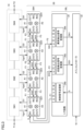
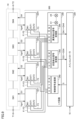
- Fig. 3 is a circuit block diagram showing the configuration of a portion of the control device 30 that is related to the control of the switch circuit 14. Note that Fig. 3 shows only a portion that is related to one-phase (U-phase) AC power.
- control device 30 includes a main controller 32, an interface (I/F) circuit 34, n gate drivers GD1 to GDn, and optical fibers F1 to F3.
- the main controller 32 judges whether the AC power supply 1 is normal or not based on the instantaneous value of the AC voltage VI detected by the voltage detector 18.
- the main controller 32 generates a control signal S for controlling the on/off of the semiconductor switches SW1 to SWn based on the judgment result. Specifically, when the AC voltage Vi is higher than the lower limit voltage, the main controller 32 judges that the AC power supply 1 is normal. In this case, the main controller 32 generates an H-level control signal S and outputs it to the I/F circuit 34.
- the gate drivers GD1 to GDn generate H-level gate signals G1 to GDn in response to the H-level control signal S. That is, the H-level control signal S corresponds to an on command (conduction command) for turning on the semiconductor switch SW.
- the main controller 32 determines that the AC power supply 1 is abnormal. In this case, the main controller 32 generates an L-level control signal S and outputs it to the I/F circuit 34. As will be described later, the gate drivers GD1 to GDn generate L-level gate signals G1 to GDn in response to the L-level control signal S. In other words, the L-level control signal S corresponds to an OFF command (shutoff command) for turning off the semiconductor switch SW.
- the I/F circuit 34 is an input/output device for exchanging signals between the main controller 32 and the gate drivers GD1 to GDn.
- the I/F circuit 34 receives a control signal S from the main controller 32.
- the I/F circuit 34 includes a control signal transmission unit 340.
- the control signal transmission unit 340 converts the control signal S, which is an electrical signal, into an optical signal and outputs it to the optical fiber F1.
- the control signal S is provided to the gate driver GD1 via the optical fiber F1.
- the I/F circuit 34 further includes a status detection signal receiving unit 342 and an abnormality detection signal receiving unit 344.
- the status detection signal receiving unit 342 receives the status detection signal DS1 from the gate driver GD1 via the optical fiber F2.
- the state detection signal DSi (i is an integer between 1 and n) is a signal that indicates the operating state (on or off) of the IGBTs Qi to Qn included in each of the semiconductor switches SWi to SWn.
- the state detection signal DSi When all of the IGBTs Qi to Qn are on, the state detection signal DSi is set to H level. When at least one of the IGBTs Qi to Qn is off, the state detection signal DSi is set to L level.
- the state detection signal DSn is set to H level when the IGBT Qn is on, and is set to L level when the IGBT Qn is off.
- the state detection signal receiver 342 converts the state detection signal DS1, which is an optical signal, into an electrical signal and outputs it to the main controller 32.
- the abnormality detection signal receiving unit 344 receives the abnormality detection signal DA1 from the gate driver GD1 via the optical fiber F3.
- the abnormality detection signal DAi (i is an integer between 1 and n) is a signal indicating the presence or absence of an abnormality in the semiconductor switches SWi to SWn. If an abnormality occurs in the semiconductor switches SWi to SWn, the abnormality detection signal DAi is set to L level. If no abnormality occurs in the semiconductor switches SWi to SWn, the abnormality detection signal DAi is set to H level.
- the abnormality detection signal DAn is set to L level when an abnormality occurs in the semiconductor switch SWn, and is set to H level when no abnormality occurs in the semiconductor switch SWn.
- the abnormality detection signal receiving unit 344 converts the abnormality detection signal DA1, which is an optical signal, into an electrical signal and outputs it to the main controller 32.
- Gate drivers GD1 to GDn are provided corresponding to semiconductor switches SW1 to SWn, respectively.
- gate driver GD has input terminals IN1 to IN3, output terminals OUT1 to OUT3, and warning lights A1 and A2.
- Gate driver GD corresponds to one embodiment of a "drive circuit.”
- the input terminal IN1 is a terminal for receiving a control signal S.
- the output terminal OUT1 is a terminal for transferring the control signal S to another gate driver GD.
- the input terminal IN2 is a terminal for receiving a state detection signal DS from another gate driver GD.
- the output terminal OUT2 is a terminal for transferring the state detection signal DS to another gate driver GD.
- the input terminal IN3 is a terminal for receiving the abnormality detection signal DA from another gate driver GD.
- the output terminal OUT3 is a terminal for transferring the abnormality detection signal DA to another gate driver GD.
- input terminal IN1 is connected to output terminal OUT1 of gate driver GDj-1 by optical fiber F1.
- Input terminal IN2 is connected to output terminal OUT2 of gate driver GDj+1 by optical fiber F2.
- Input terminal IN3 is connected to output terminal OUT3 of gate driver GDj+1 by optical fiber F3.
- the input terminal IN1 is connected to the control signal transmission unit 340 of the I/F circuit 34 by an optical fiber F1.
- the input terminal IN2 is connected to the output terminal OUT2 of the gate driver GD2 by an optical fiber F2.
- the input terminal IN3 is connected to the output terminal OUT3 of the gate driver GD2 by an optical fiber F3.
- the output terminal OUT2 is connected to the status detection signal receiving unit 342 of the I/F circuit 34 by an optical fiber F2.
- the output terminal OUT3 is connected to the abnormality detection signal receiving unit 344 by an optical fiber F3.
- input terminal IN1 is connected to output terminal OUT1 of gate driver GDn-1 (GD3 in FIG. 3) by optical fiber F1.
- Output terminal OU1 and input terminals IN1 and IN2 are not connected.
- the gate driver GD is provided with warning lights A1 and A2.
- the warning lights A1 and A2 are notification components for notifying the user of the power supply device 10 of an abnormality that has occurred in the semiconductor switch SW. As described below, the warning light A1 is turned on when the semiconductor switch SW cannot be turned on or off in response to the control signal S due to a failure of the IGBT Q or a failure of the driver that drives the IGBT Q.
- the warning light A2 is turned on when a communication failure occurs in the control signal S or the status detection signal DS due to damage to the optical fibers F1 and F2, as described below.
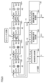
- optical fibers F1 to F3 3 the I/F circuit 34 and the gate drivers GD1-GDn are connected in series by optical fibers F1-F3.
- the optical fiber F1 is a signal line for transmitting a control signal S from the I/F circuit 34 to the gate drivers GD1-GDn.
- the control signal S output from the I/F circuit 34 is transmitted via the optical fiber F1 to the gate drivers GD1, GD2, ... in that order, up to the gate driver GDn.
- the optical fiber F1 corresponds to one example of a "first communication line".
- the optical fiber F2 is a signal line for transmitting the state detection signal DS from the gate drivers GD1 to GDn to the I/F circuit 34.
- the state detection signal DS output from the gate driver GDn is transmitted to the gate driver GD1 in the order of gate drivers GDn-1, GDn-2, etc. via the optical fiber F2, and is sent from the gate driver GD1 to the I/F circuit 34 via the optical fiber F2.
- the gate driver GDj is configured to generate a state detection signal DSj based on the state detection signal DSj+1 input to the input terminal IN2 and the operating state of the IGBTQ of the corresponding semiconductor switch SW, and to output the generated state detection signal DSj from the output terminal OUT2 to the gate driver GDj-1.
- the optical fiber F2 corresponds to one embodiment of the "second communication line".
- the optical fiber F3 is a signal line for transmitting the abnormality detection signal GA from the gate drivers GD1 to GDn to the I/F circuit 34.
- the abnormality detection signal DA output from the gate driver GDn is transmitted to the gate driver GD1 in the order of gate drivers GDn-1, GDn-2, etc. via the optical fiber F3, and is sent from the gate driver GD1 to the I/F circuit 34 via the optical fiber F3.
- the gate driver GDj is configured to generate an abnormality detection signal DAj based on the abnormality detection signal DAj+1 input to the input terminal IN3 and the abnormality detection result of the corresponding semiconductor switch SW, and to output the generated abnormality detection signal DAj from the output terminal OUT2 to the gate driver GDj-1.
- the optical fiber F3 corresponds to one embodiment of the "third communication line".
- the main controller 32 and I/F circuit 34 are low-voltage components 30L that operate on a power supply voltage of several volts.
- the gate drivers GD1 to GDn are high-voltage components 30H that operate on a power supply voltage of several kV.
- optical fibers F1 to F3 as communication lines for transmitting signals between the I/F circuit 34 and the gate driver GD1
- electrical insulation between the high-voltage components 30H and the low-voltage components 30L can be ensured.
- the wiring length of the optical fibers F1 to F3 connecting the I/F circuit 34 and the gate driver GD1 may reach several meters.
- the wiring length of the optical fibers F1 to F3 connected to the gate drivers GD2 to GDn can be shortened to about several tens of centimeters. This prevents the wiring from becoming complicated due to an increase in the number n of semiconductor switches SW.
- FIG. 4 is a circuit block diagram showing an example of the configuration of gate driver GD. Since gate drivers GD1 to GDn have the same configuration, FIG. 4 explains the configuration of gate driver GD2 as a representative of them.
- the gate driver GD2 is provided in correspondence with the semiconductor switch SW2.
- the gate driver GD2 has a driver 40, a determiner 42, an abnormality detection circuit 44, and warning lights A1 and A2.
- the input terminal IN1 receives a control signal S from the gate driver GD1.
- the control signal S is transferred to the driver 40, the abnormality detection circuit 44, and the output terminal OUT1.
- the control signal S is provided from the output terminal OUT1 via the optical fiber F1 to the input terminal IN1 of the gate driver GD3.
- the driver 40 generates a gate signal G2 based on the control signal S and inputs the generated gate signal G2 to the gate of the IGBT Q2.
- the driver 40 generates an H-level gate signal G2 in response to an H-level control signal S (on command), and generates an L-level gate signal G2 in response to an L-level control signal S (off command).
- the gate voltage Vge is a voltage (gate drive voltage) higher than the threshold voltage Vth, whereas when IGBT Q2 is off, the gate voltage Vge is a voltage lower than the threshold voltage Vth.
- the determiner 42 receives a signal Vge2 from the semiconductor switch SW2, which indicates the magnitude of the gate voltage Vge of IGBT Q2. Based on the signal Vge2, the determiner 42 determines whether IGBT Q2 is in the on or off state, and outputs a signal DET indicating the determination result to the abnormality detection circuit 44. Specifically, when the gate voltage Vge is higher than the threshold voltage Vth, it is determined that IGBT Q2 is in the off state, and the signal DET is set to the H level. On the other hand, when the gate voltage Vge is lower than the threshold voltage Vth, it is determined that IGBT Q2 is in the off state, and the signal DET is set to the L level.
- the input terminal IN2 receives a state detection signal DS3 from the gate driver GD3.
- the state detection signal DS3 is a state detection signal DS generated by the gate driver GD3, and is a signal that indicates whether the IGBTs Q3 to Qn included in the semiconductor switches SW3 to SWn, respectively, are in an on or off state.
- the state detection signal DS3 is set to an H level.
- the state detection signal DS3 is set to an L level.
- the input terminal IN3 receives an abnormality detection signal DA3 from the gate driver GD3.
- the abnormality detection signal DA3 is the abnormality detection signal DA generated by the gate driver GD3, and is a signal that indicates the presence or absence of an abnormality in the semiconductor switches SW3 to SWn. If an abnormality occurs in the semiconductor switches SW3 to SWn, the abnormality detection signal DA3 is set to L level. If no abnormality occurs in the semiconductor switches SW3 to SWn, the abnormality detection signal DA3 is set to H level.
- the state detection signal DS3 and the abnormality detection signal DA3 are transferred to the abnormality detection circuit 44.
- the abnormality detection circuit 44 generates a state detection signal DS2 and an abnormality detection signal DA2 based on the control signal S, the signal DET, the state detection signal DS3, and the abnormality detection signal DA3.
- the state detection signal DS2 is provided from the output terminal OUT2 via the optical fiber F2 to the input terminal IN2 of the gate driver GD1.
- the abnormality detection signal DA2 is provided from the output terminal OUT3 via the optical fiber F3 to the input terminal IN3 of the gate driver GD1.
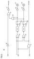
- FIG. 5 is a circuit diagram showing an example of the configuration of the abnormality detection circuit 44 shown in FIG.
- the abnormality detection circuit 44 includes exclusive OR (XOR) circuits 50 and 52, time limit circuits 54 and 56, flip-flops 58 and 60, OR circuits 62 and 70, NOT circuits 64, 66, 68 and 72, and an AND circuit 74.
- XOR exclusive OR
- the XOR circuit 50 receives the control signal S at its first input terminal and the output signal DET of the determiner 42 at its second input terminal.
- the XOR circuit 50 calculates the exclusive OR of the two input signals and outputs a signal indicating the calculation result. Specifically, when the value of the control signal S matches the value of the signal DET, the XOR circuit 50 outputs an L-level signal. When the value of the control signal S does not match the value of the signal DET, the XOR circuit 50 outputs an H-level signal.
- the output signal of the XOR circuit 50 is set to L level.
- the control signal S and the signal DET are both at L level, i.e., when the IGBT Q2 is normally turned off in response to an OFF command, the output signal of the XOR circuit 50 is set to L level.
- the output signal of the XOR circuit 50 is set to H level. In this way, an H level output signal indicates that the operation of the semiconductor switch SW2 in response to the control signal S is abnormal.
- the time limit circuit 54 is realized by, for example, a counter, and counts the time during which the XOR circuit 50 outputs an H-level signal. When the time during which the XOR circuit 50 outputs an H-level signal exceeds a predetermined time, the time limit circuit 54 outputs a signal with a value of "1.” Thus, when the abnormal operation of the semiconductor switch SW2 continues for a predetermined time or longer, the time limit circuit 54 outputs a signal with a value of "1.”
- the timer circuit 54 when the XOR circuit 50 outputs an L-level signal, or when the time during which the XOR circuit 50 outputs an H-level signal does not reach the predetermined time, the timer circuit 54 outputs a signal with a value of "0.” As a result, when the operation of the semiconductor switch SW2 is normal, or when the state in which the operation of the semiconductor switch SW2 is abnormal does not continue for the predetermined time, the timer circuit 54 outputs a signal with a value of "0.”
- the specified time is set taking into consideration the fact that there may be a difference in the timing of receiving the control signal S between the gate drivers GD1 to GDn.
- the specified time is set to be equal to or longer than the time required for the gate driver GD4 to receive the control signal S sent from the I/F circuit 34.
- the NOT circuit 64 inverts the output signal of the flip-flop 58 and outputs it. For example, when a signal with a value of "1" is input to the NOT circuit 64, it outputs a signal with a value of "0", and when a signal with a value of "0" is input, it outputs a signal with a value of "1".
- the warning light A1 is turned on when it receives a signal with a value of "0" from the NOT circuit 64.
- the warning light A1 is turned off when it receives a signal with a value of "1" from the NOT circuit 64.
- the warning light A1 is turned on when the operation of the semiconductor switch SW2 remains abnormal for a predetermined period of time.
- the warning light A1 corresponds to one embodiment of a "first notification member" for notifying the user that the operation of the semiconductor switch SW2 is abnormal in response to the control signal S provided to the gate driver GD2.
- AND circuit 74 receives output signal DET from determiner 42 at a first input terminal, and receives state detection signal DS3 from gate driver GD3 at a second input terminal.
- state detection signal DS3 is the state detection signal DS generated by gate driver GD3, and is a signal that indicates whether IGBTs Q3 to Qn included in semiconductor switches SW3 to SWn, respectively, are in an on or off state.
- state detection signal DS3 is set to H level.
- state detection signal DS3 is set to L level.
- the AND circuit 74 calculates the logical product of the two input signals and outputs a state detection signal DS2 indicating the calculation result.
- the AND circuit 74 outputs a state detection signal DS2 at H level.
- the AND circuit 74 outputs a state detection signal DS2 at L level. Therefore, when all of the IGBTs Q2 to Qn are in the ON state, the state detection signal DS2 is set to H level. On the other hand, when at least one of the IGBTs Q2 to Qn is in the OFF state, the state detection signal DS2 is set to L level.
- the XOR circuit 52 receives the control signal S at its first input terminal and the state detection signal DS2 at its second input terminal.
- the XOR circuit 52 calculates the exclusive OR of the two input signals and outputs a signal indicating the calculation result.
- the XOR circuit 52 outputs an L-level signal.
- the XOR circuit 52 outputs an H-level signal.
- the output signal of the XOR circuit 52 is set to L level.
- the control signal S and the state detection signal DS2 are both at H level, i.e., when the IGBTs Q2 to Qn are normally turned on in response to an ON command, the output signal of the XOR circuit 52 is set to L level.
- the control signal S and the state detection signal DS2 are both at L level, i.e., when at least one of the IGBTs Q2 to Qn is turned off in response to an OFF command, the output signal of the XOR circuit 52 is set to L level.
- the output signal of the XOR circuit 52 is set to H level.
- the control signal S is at L level and the state detection signal DS2 is at H level, that is, when all of the IGBTs Q2 to Qn are turned on contrary to the OFF command, the output signal of the XOR circuit 52 is set to H level. In this way, an H level output signal indicates that the control signal S and the operation of the semiconductor switches SW2 to SWn do not match.
- the time limit circuit 56 counts the time during which the XOR circuit 52 outputs an H-level signal. If the time during which the XOR circuit 52 outputs an H-level signal exceeds a predetermined time, the time limit circuit 56 outputs a signal with a value of "1.” This means that if a state in which the control signal S and the operation of the semiconductor switches SW2 to SWn do not match continues for a predetermined time or longer, the time limit circuit 56 outputs a signal with a value of "1.”
- the timer circuit 56 when the XOR circuit 52 outputs an L-level signal, or when the time during which the XOR circuit 52 outputs an H-level signal is less than the predetermined time, the timer circuit 56 outputs a signal with a value of "0".
- the control signal S matches the operation of the semiconductor switches SW2 to SWn, or when the state in which the control signal S does not match the operation of the semiconductor switches SW2 to SWn does not continue for the predetermined time
- the timer circuit 56 outputs a signal with a value of "0".
- the predetermined time is set taking into consideration the occurrence of a lag in the timing of receiving the control signal S between the gate drivers GD1 to GDn.
- the NOT circuit 66 inverts the output signal of the flip-flop 60 and outputs it.
- the warning light A2 is turned on when the NOT circuit 64 receives a signal of value "0" from the circuit 66.
- the warning light A2 is turned off when the NOT circuit 64 receives a signal of value "1".
- the warning light A2 is turned on when the state in which the control signal S does not match the operation of the semiconductor switches SW2 to SWn continues for more than a predetermined time.
- the warning light A2 corresponds to one embodiment of a "second notification member" for notifying the user of an abnormality in which the control signal S given to the gate driver GD2 does not match the operation of the semiconductor switches SW2 to SWn.
- OR circuit 62 receives the output signal of flip-flop 58 at its first input terminal, and the output signal of flip-flop 60 at its second input terminal. OR circuit 62 calculates the logical sum of the two input signals, and outputs a signal indicating the calculation result. When at least one of the output signals of flip-flop 58 and flip-flop 60 is at H level (i.e., when the value is "1"), OR circuit 62 outputs an H level signal.
- the output signal of flip-flop 58 is held at H level in response to the output signal of timer circuit 54. Also, if the state in which the control signal S and the operation of semiconductor switches SW2 to SWn do not match continues for more than a predetermined time, the output signal of flip-flop 60 is held at H level in response to the output signal of timer circuit 56.
- the NOT circuit 68 inverts the abnormality detection signal DA3 input from the gate driver GD3 and outputs it.
- the abnormality detection signal DA3 is a signal that indicates the presence or absence of an abnormality in the semiconductor switches SW3 to SWn. If an abnormality occurs in at least one of the semiconductor switches SW3 to SWn, the abnormality detection signal DA3 is set to L level. If no abnormality occurs in any of the semiconductor switches SW3 to SWn, the abnormality detection signal DA3 is set to H level.
- an H-level abnormality detection signal DA3 is input to the NOT circuit 68, it outputs an L-level signal, and when an L-level abnormality detection signal DA3 is input, it outputs an H-level signal.
- the OR circuit 70 receives the output signal of the NOT circuit 68 at its first input terminal, and receives the output signal of the OR circuit 62 at its second input terminal.
- the OR circuit 70 calculates the logical sum of the two input signals, and outputs a signal indicating the calculation result.
- the OR circuit 70 outputs an H level signal.
- the output signal of the OR circuit 70 is set to H level when at least one of the following conditions is met: (i) when the abnormality detection signal DA3 is at L level, i.e., when an abnormality has occurred in the semiconductor switches SW3 to SWn, or (ii) when an abnormality has occurred in the semiconductor switch SW2.
- the output signal of the OR circuit 70 is set to L level when all of the following conditions are met: (iii) when the abnormality detection signal DA3 is at H level, i.e., when the semiconductor switches SW3 to SWn are normal, or (iv) when the semiconductor switch SW2 is normal.
- the NOT circuit 72 inverts the output signal of the OR circuit 70 to generate the abnormality detection signal DA2.
- the NOT circuit 70 outputs an L-level abnormality detection signal DA2
- an L-level signal is input from the OR circuit 70
- the NOT circuit 70 outputs an H-level abnormality detection signal DA2.
- the L-level abnormality detection signal DA2 satisfies at least one of (i) and (iii) above, indicating that an abnormality has occurred in at least one of the semiconductor switches SW2 to SWn.
- the H-level abnormality detection signal DA2 satisfies all of (iii) and (iv) above, indicating that all of the semiconductor switches SW2 to SWn are normal.
- the abnormality detection circuit 44 in the gate driver GD2 is configured to turn on the warning light A1 if it detects an abnormality in the operation of the semiconductor switch SW2 in response to the control signal S provided to the gate driver GD2.
- the abnormality detection circuit 44 is also configured to turn on the warning light A2 if it detects a mismatch between the control signal S provided to the gate driver GD2 and the operation of the semiconductor switches SW2 to SWn.
- the abnormality detection circuit 44 is further configured to turn on the warning lights A1 and A2, and generate an L-level abnormality detection signal DA2 when it determines that an abnormality has occurred in the semiconductor switch SW2.
- the abnormality detection circuit 44 is configured to output a high-level state detection signal DS2 when all of the IGBTs Q2 to Qn are in the on state, and to generate a low-level state detection signal DS2 when at least one of the IGBTs Q2 to Qn is in the off state.
- the state detection signal DS2 is provided from the output terminal OUT2 via the optical fiber F2 to the input terminal IN2 of the gate driver GD1.
- the abnormality detection signal DA2 is provided from the output terminal OUT3 via the optical fiber F3 to the input terminal IN3 of the gate driver GD1.
- the gate driver GD1 also follows a similar procedure to control the abnormality lights A1 and A2 based on the control signal S, the signal DET, the state detection signal DS2, and the abnormality detection signal DA2, and generates the state detection signal DS1 and the abnormality detection signal DA1.
- the state detection signal DS1 is provided from the output terminal OUT2 via the optical fiber F2 to the state detection signal receiving unit 342 of the I/F circuit 34.
- the abnormality detection signal DA1 is provided from the output terminal OUT3 via the optical fiber F3 to the abnormality detection signal receiving unit 344 of the I/F circuit 34.
- FIG. 6 is a diagram for explaining the abnormality detection operation of the gate drivers GD1 to GDn. In Figure 6, it is assumed that the driver 40 of the gate driver GD2 has failed.
- the gate driver GD2 receives a control signal S from the gate driver GD1 via the optical fiber F1.
- the gate driver GD2 also receives a state detection signal DS3 and an abnormality detection signal DA3 from the gate driver GD3 via the optical fibers F2 and F3.
- the driver 40 is normal and turns on or off the IGBTs Q3 to Qn included in the semiconductor switches SW3 to SWn, respectively, in response to the control signal S. Therefore, when the control signal S is at H level, the abnormality detection circuit 44 of gate driver GD2 receives an H-level state detection signal DS3. The abnormality detection circuit 44 further receives an H-level abnormality detection signal DA3.
- the driver 40 Inside the gate driver GD2, the driver 40 generates a gate signal G2 based on the control signal S and inputs it to the gate of IGBT Q2. However, if the driver 40 malfunctions and is unable to generate the gate signal G2 normally, it may happen that IGBT Q2 is not turned on despite an H-level control signal S (on command), or that IGBT Q2 is not turned off despite an L-level control signal S (off command).
- the abnormality detection circuit 44 determines that an abnormality has occurred in the operation of semiconductor switch SW2 in response to the control signal S in response to the state in which the value of the control signal S and the value of the signal DET do not match for a predetermined period of time, as shown in FIG. 5. As a result, the warning light A1 of the gate driver GD2 is turned on.
- the abnormality detection circuit 44 generates an L-level state detection signal DS2 because IGBT Q2 of IGBTs Q2 to Qn is in the off state contrary to the H-level control signal S.
- the abnormality detection circuit 44 determines that a mismatch has occurred between the control signal S and the operation of the semiconductor switches SW2 to SWn. As a result, the warning light A2 of the gate driver GD2 is turned on.
- the abnormality detection circuit 44 determines that an abnormality has occurred in the semiconductor switch SW2 and generates an L-level abnormality detection signal DA2.
- the L-level state detection signal DS2 and the L-level abnormality detection signal DA2 are provided to the abnormality detection circuit 44 of the gate driver GD1 via optical fibers F2 and F3, respectively.
- the driver 40 is normal, so the IGBT Q1 of the semiconductor switch SW1 is turned on in response to the H-level control signal S. Because the value of the control signal S matches the value of the signal DET, the abnormality detection circuit 44 determines that the semiconductor switch SW2 is normal. As a result, the warning light A1 is turned off.
- the abnormality detection circuit 44 generates an L-level state detection signal DS1 based on the L-level state detection signal DS2 and the H-level signal DET.
- the L-level state detection signal DS1 indicates that at least one of the IGBTs Q1 to Qn is in the off state.
- the abnormality detection circuit 44 determines that a mismatch has occurred between the control signal S and the operation of the semiconductor switches SW1 to SWn. As a result, the warning light A2 of the gate driver GD1 is turned on.
- an H-level signal is sent to OR circuit 70.
- an H-level abnormality detection signal DA2 is sent to OR circuit 70 from gate driver GD2 via NOT circuit 68.
- the abnormality detection circuit 44 determines that an abnormality has occurred in semiconductor switches SW1 to SWn, and generates an L-level abnormality detection signal DA1.
- the L-level state detection signal DS1 and the L-level abnormality detection signal DA1 are sent to I/F circuit 34 via optical fibers F2 and F3, respectively.
- the warning lights A1 and A2 provided on the gate driver GD2 will light up, and the warning light A2 provided on the gate driver GD1 will light up.
- the user can detect that an abnormality has occurred in the operation of the semiconductor switch SW2 in response to the control signal S. Furthermore, when the warning light A2 of the gate driver GD2 is lit, the user can detect that a mismatch has occurred between the control signal S and the operation of the semiconductor switches SW2 to SWn, which has been caused by an abnormality in the operation of the semiconductor switch SW2.
- the user can detect that the semiconductor switch SW1 is normal and that an inconsistency has occurred between the control signal S and the operation of the semiconductor switches SW1 to SWn due to an operational abnormality in the semiconductor switch SW2.
- FIG. 7 is a diagram for explaining the abnormality detection operation of the gate drivers GD1 to GDn. Fig. 7 assumes that the optical fiber F1 connecting the gate drivers GD2 and GD3 is cut.
- the control signal S cannot be transmitted from the gate driver GD2 to the gate driver GD3, and the gate drivers GD3 to GDn cannot receive the control signal S. Therefore, when an H-level control signal S (on command) is output from the I/F circuit 34, an on command is given to the gate drivers GD1 and GD2, but an on command is not given to the gate drivers GD3 to GDn.
- the gate drivers GD1 and GD2 turn on the IGBTs Q1 and Q2 of the semiconductor switches SW1 and SW2 in response to the H-level control signal S. Meanwhile, the gate drivers GD3 to GDn keep the IGBTs Q3 to Qn of the semiconductor switches SW3 to SWn in the off state in response to the L-level control signal S.
- the IGBTs Q1 to Qn of the semiconductor switches SW1 to SWn are operating normally in response to the control signal S provided. Therefore, the warning light A1 is turned off in all of the gate drivers GD1 to GDn.
- the abnormality detection circuit 44 Inside the gate driver GD2, the abnormality detection circuit 44 generates an L-level state detection signal DS2 in response to an L-level state detection signal DS3 from the gate driver GD3. Then, in response to the state in which the value of the control signal S and the value of the state detection signal DS2 do not match continuing for a predetermined period of time, the abnormality detection circuit 44 determines that a mismatch has occurred between the control signal S and the operation of the semiconductor switches SW2 to SWn. As a result, the warning light A2 of the gate driver GD2 is turned on.
- the abnormality detection circuit 44 determines that an abnormality has occurred in the semiconductor switch SW2, and generates an L-level abnormality detection signal DA2.
- the L-level state detection signal DS2 and the L-level abnormality detection signal DA2 are provided to the abnormality detection circuit 44 of the gate driver GD1 via optical fibers F2 and F3, respectively.
- the abnormality detection circuit 44 Inside the gate driver GD1, the abnormality detection circuit 44 generates an L-level state detection signal DS1 in response to an L-level state detection signal DS2.
- the L-level state detection signal DS1 indicates that at least one of the IGBTs Q1 to Qn is in the off state.
- the abnormality detection circuit 44 determines that a mismatch has occurred between the control signal S and the operation of the semiconductor switches SW1 to SWn. As a result, the warning light A2 of the gate driver GD1 is turned on.
- the abnormality detection circuit 44 determines that an abnormality has occurred in the semiconductor switch SW1, and generates an L-level abnormality detection signal DA1.
- the L-level state detection signal DS1 and the L-level abnormality detection signal DA1 are provided to the I/F circuit 34 via optical fibers F2 and F3, respectively.
- the user can detect that there is an operational inconsistency between semiconductor switches SW1 and SW2 and semiconductor switches SW3 and SW4. The user can then infer that this operational inconsistency is caused by a communication error between gate drivers GD2 and GD3.
- Fig. 8 is a diagram for explaining the abnormality detection operation of the gate drivers GD1 to GDn. Fig. 8 assumes that the optical fiber F2 connecting the gate drivers GD2 and GD3 is cut.
- the state detection signal DS3 cannot be transmitted from the gate driver GD3 to the gate driver GD2.
- the gate driver GD2 cannot generate the state detection signal DS2 using the state detection signal DS3.
- the gate drivers GD1 to GDn When an H-level control signal S (ON command) is output from the I/F circuit 34, the gate drivers GD1 to GDn turn on the IGBTs Q1 to Qn included in the semiconductor switches SW1 to SWn, respectively, in response to the H-level control signal S. Since the IGBTs Q1 to Qn are operating normally in response to the control signal S thus provided, the warning light A1 is turned off in all of the gate drivers GD1 to GDn.
- the abnormality detection circuit 44 generates an L-level state detection signal DS2 in response to the L-level state detection signal DS3. Then, in response to the state in which the value of the control signal S and the value of the state detection signal DS2 do not match continuing for a predetermined period of time, the abnormality detection circuit 44 determines that a mismatch has occurred between the control signal S and the operation of the semiconductor switches SW2 to SWn. As a result, the warning light A2 of the gate driver GD2 is turned on.
- the abnormality detection circuit 44 determines that an abnormality has occurred in the semiconductor switch SW2, and generates an L-level abnormality detection signal DA2.
- the L-level state detection signal DS2 and the L-level abnormality detection signal DA2 are provided to the abnormality detection circuit 44 of the gate driver GD1 via optical fibers F2 and F3, respectively.
- the abnormality detection circuit 44 generates an L-level state detection signal DS1 in response to an L-level state detection signal DS2.
- the L-level state detection signal DS1 indicates that at least one of the IGBTs Q1 to Qn is in the off state. Then, in response to the state in which the value of the control signal S and the value of the state detection signal DS1 do not match continuing for a predetermined period of time, it is determined that a mismatch has occurred between the control signal S and the operation of the semiconductor switches SW1 to SWn. As a result, the warning light A2 of the gate driver GD1 is turned on.
- the abnormality detection circuit 44 determines that an abnormality has occurred in the semiconductor switch SW1, and generates an L-level abnormality detection signal DA1.
- the L-level state detection signal DS1 and the L-level abnormality detection signal DA1 are provided to the I/F circuit 34 via optical fibers F2 and F3, respectively.
- the user can detect that there is an operational inconsistency between semiconductor switches SW1 and SW2 and semiconductor switches SW3 and SW4. The user can then infer that this operational inconsistency is caused by a communication error between gate drivers GD2 and GD3.
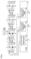
- FIG. 9 is a diagram showing the general configuration of a power supply device according to a comparative example.
- FIG. 9 shows the configuration of the portion of the control device 300 included in the power supply device according to the comparative example that is related to the control of the switch circuit 14. Note that FIG. 9 only shows the portion related to one-phase (U-phase) AC power.
- the control device 300 includes a main controller 320, an I/F circuit 330, n gate drivers GD1 to GDn, and optical fibers F1 to F3.
- the control device 300 differs from the control device 30 shown in FIG. 3 in the configuration of the gate driver GD and the wiring of the optical fibers F1 to F3.
- optical fibers F1 to F3 are provided between each of the gate drivers GD1 to GDn and the I/F circuit 330.
- the gate drivers GD1 to GDn are connected in parallel to each other with respect to the I/F circuit 330.
- each of the gate drivers GD1 to GDn can directly exchange signals with the I/F circuit 330, so signal delays are reduced compared to the present embodiment.
- optical fibers F1 to F3 which are several meters long, are connected to all of the gate drivers GD1 to GDn, there is a concern that the wiring will become more complicated as the number n of semiconductor switches SW increases.
- a state detection signal DS indicating the on/off state of the corresponding semiconductor switch SW is input from each gate driver GD to the I/F circuit 330, and the I/F circuit 330 can detect an operational abnormality of the semiconductor switch SW in response to the control signal S by comparing the control signal S with the state detection signal DS for each gate driver GD. Then, by lighting the warning light A corresponding to the semiconductor switch SW that is operating abnormally, out of the warning lights A1-An provided corresponding to the semiconductor switches SW1-SWn, respectively, the user can be notified of which semiconductor switch SW has an abnormality.
- the gate drivers GD1 to GDn are connected in series to the I/F circuit 34, which makes it possible to shorten the wiring length of the optical fibers F1 to F3 connected to the gate drivers GD2 to GDn. This makes it possible to prevent the wiring from becoming complicated due to an increase in the number n of semiconductor switches SW.
- each gate driver GD is provided with a warning light A1 (first warning member) for warning that the operation of the semiconductor switch SW in response to a given control signal S is abnormal, and a warning light A1 (second warning member) for warning that the operation of the given control signal S does not match that of the multiple semiconductor switches SW including the semiconductor switch SW.
- a warning light A1 first warning member
- a warning light A1 second warning member
- the user can identify the location where the failure is occurring.
- the power supply device 10 makes it possible to identify the content and location of an abnormality that has occurred in a power supply device having multiple semiconductor switches connected in series, without complicating the device configuration.
Landscapes
- Engineering & Computer Science (AREA)
- Power Engineering (AREA)
- Business, Economics & Management (AREA)
- Emergency Management (AREA)
- Power Conversion In General (AREA)
- Stand-By Power Supply Arrangements (AREA)
- Protection Of Static Devices (AREA)
- Emergency Protection Circuit Devices (AREA)
Abstract
Description
図1は、実施の形態に係る電源装置の概略構成を示す図である。
次に、実施の形態に係る電源装置10の動作について説明する。
図3は、制御装置30のうちスイッチ回路14の制御に関連する部分の構成を示す回路ブロック図である。なお、図3では、一相(U相)の交流電力に関連する部分のみが示されている。
メインコントローラ32は、電圧検出器18により検出される交流電圧VIの瞬時値に基づいて、交流電源1が正常であるか否かを判定する。メインコントローラ32は、判定結果に基づいて、半導体スイッチSW1~SWnのオンオフを制御するための制御信号をSを生成する。具体的には、交流電圧Viが下限電圧よりも高い場合には、メインコントローラ32は、交流電源1が正常であると判定する。この場合、メインコントローラ32は、Hレベルの制御信号Sを生成してI/F回路34に出力する。後述するように、ゲートドライバGD1~GDnは、Hレベルの制御信号Sに応答して、Hレベルのゲート信号G1~GDnをそれぞれ生成する。すなわち、Hレベルの制御信号Sは、半導体スイッチSWをオンするためのオン指令(導通指令)に相当する。
I/F回路34は、メインコントローラ32およびゲートドライバGD1~GDnとの間で信号を遣り取りするための入出力装置である。I/F回路34は、メインコントローラ32から制御信号Sを受信する。I/F回路34は、制御信号送信部340を含む。制御信号送信部340は、電気信号である制御信号Sを光信号に変換し、光ファイバF1に出力する。制御信号Sは、光ファイバF1を経由してゲートドライバGD1に与えられる。
ゲートドライバGD1~GDnは、半導体スイッチSW1~SWnにそれぞれ対応して設けられている。以下では、ゲートドライバGD1~GDnを包括的に表記する場合には、単に「ゲートドライバGD」とも称する。ゲートドライバGDは、入力端子IN1~IN3と、出力端子OUT1~OUT3と、警告灯A1,A2とを有している。ゲートドライバGDは「駆動回路」の一実施例に対応する。
図3に示すように、I/F回路34およびゲートドライバGD1~GDnは、光ファイバF1~F3によって直列に接続されている。光ファイバF1は、I/F回路34からゲートドライバGD1~GDnに制御信号Sを伝送するための信号線である。I/F回路34から出力された制御信号Sは、光ファイバF1を経由して、ゲートドライバGD1,GD2・・・の順に、ゲートドライバGDnまで伝送される。光ファイバF1は「第1の通信線」の一実施例に対応する。
次に、図3に示したゲートドライバGDの構成例について説明する。
図5は、図4に示した異常検出回路44の構成例を示す回路図である。
次に、図3および図4に示したゲートドライバGD1~GDnによるスイッチ回路14の異常検出動作について説明する。ゲートドライバGD1~GDは、以下に例示する3種類の異常を検出することが可能に構成されている。
最初に、ゲートドライバGD1~GDnのうちの何れか1つにおいて、ドライバ40またはIGBTQの故障が生じた場合の異常検出動作を説明する。図6は、ゲートドライバGD1~GDnの異常検出動作を説明するための図である。図6では、ゲートドライバGD2のドライバ40が故障した場合を想定している。
次に、光ファイバF1が損傷したことで、制御信号Sの通信異常が生じた場合の異常検出動作を説明する。図7は、ゲートドライバGD1~GDnの異常検出動作を説明するための図である。図7では、ゲートドライバGD2とゲートドライバGD3とを接続する光ファイバF1が切断された場合を想定している。
次に、光ファイバF2が損傷したことによって、状態検出信号DSの通信異常が生じた場合異常検出動作を説明する。図8は、ゲートドライバGD1~GDnの異常検出動作を説明するための図である。図8では、ゲートドライバGD2とゲートドライバGD3とを接続する光ファイバF2が切断された場合を想定している。
以下に、比較例に係る電源装置と対比しながら、本実施の形態に係る電源装置10の作用効果について説明する。
Claims (8)
- nを2以上の整数とし、iを1以上n-1以下の整数としたとき、
第1および第2の端子間に直列接続された第1から第nの半導体スイッチと、
前記第1から第nの半導体スイッチにそれぞれ対応して設けられ、制御信号に応答して、対応する半導体スイッチを駆動する、第1から第nの駆動回路と、
前記第1から第nの駆動回路と信号を授受するインターフェイス回路と、
前記インターフェイス回路と前記第1から第nの駆動回路とを直列に接続する第1および第2の通信線とを備え、
前記第1の通信線は、前記制御信号を、前記インターフェイス回路から前記第1の駆動回路を経由して前記第nの駆動回路まで順次伝送するように構成され、
前記第2の通信線は、半導体スイッチの動作状態を示す状態検出信号を、前記第nの駆動回路から前記第1の駆動回路を経由して前記インターフェイス回路まで順次伝送するように構成され、
第iの駆動回路は、
第(i-1)の駆動回路から受信した前記制御信号に応答して、第iの半導体スイッチを駆動するドライバと、
第iの半導体スイッチの異常を検出するための異常検出回路と、
第1および第2の報知部材とを含み、
前記異常検出回路は、
前記制御信号および前記第iの半導体スイッチの動作状態に基づいて、前記第iの半導体スイッチの異常を検出し、検出結果を前記第1の報知部材を用いて報知し、
前記第iの半導体スイッチの動作状態と、第(i+1)の駆動回路から受信した、第(i+1)から第nの半導体スイッチの動作状態を示す前記状態検出信号とに基づいて、前記第iから第nの半導体スイッチの動作状態を示す前記状態検出信号を生成し、
前記制御信号および生成した前記状態検出信号に基づいて、前記制御信号と前記第iから第nの半導体スイッチの動作状態との不一致を検出し、検出結果を前記第2の報知部材を用いて報知する、電源装置。 - 前記インターフェイス回路と前記第1から第nの駆動回路とを直列に接続する第3の通信線をさらに備え、
前記第3の通信線は、半導体スイッチの異常の有無を示す異常検出信号を、前記第nの駆動回路から前記第1の駆動回路を経由して前記インターフェイス回路まで順次伝送するように構成され、
前記第iの駆動回路において、前記異常検出回路は、
前記第iの半導体スイッチの異常、および、前記制御信号と前記第iから第nの半導体スイッチの動作状態との不一致の少なくとも一方が検出された場合、または、前記第(i+1)の駆動回路から、前記第(i+1)から第nの半導体スイッチの異常を示す前記異常検出信号を受信した場合に、前記第iから第nの半導体スイッチの異常を示す前記状態検出信号を生成する、請求項1に記載の電源装置。 - 前記異常検出回路は、
前記制御信号に応答して前記第iの半導体スイッチが正常に動作しない状態が第1の所定時間継続したことに応じて、前記第iの半導体スイッチの異常を検出し、
前記制御信号の値と前記状態検出信号の値とが一致しない状態が第2の所定時間継続したことに応じて、前記制御信号と前記第iから第nの半導体スイッチの動作状態との不一致を検出する、請求項1または2に記載の電源装置。 - 前記第1から第nの半導体スイッチの各々は、主電極と制御電極とを有する半導体スイッチング素子を含み、
前記第iの駆動回路において、
前記ドライバは、前記制御信号に応じた駆動信号を前記半導体スイッチング素子の前記制御電極へ入力し、
前記異常検出回路は、前記制御電極および前記主電極間の電圧に基づいて、前記第iの半導体スイッチの動作状態を検出する、請求項1に記載の電源装置。 - 前記第1から第3の通信線の各々は、光ファイバである、請求項2に記載の電源装置。
- 前記第1および第2の報知部材の各々は、警告灯である、請求項1に記載の電源装置。
- 前記第1の端子は、交流電源から供給される交流電力を受け、
前記第2の端子は、交流電力によって駆動される負荷に接続され、
前記インターフェイス回路は、前記交流電源から交流電圧が正常に供給されている第1の場合には、前記第1から第nの半導体スイッチをオンさせるための前記制御信号を生成して前記第1の通信線に出力し、前記交流電源から交流電圧が正常に供給されていない第2の場合には、前記第1から第nの半導体スイッチをオフさせるための前記制御信号を生成して前記第1の通信線に出力する、請求項1に記載の電源装置。 - 前記第2の端子に接続された双方向コンバータをさらに備え、
前記双方向コンバータは、前記第1の場合には、前記交流電源から前記第1から第nの半導体スイッチを介して供給される交流電力を直流電力に変換して電力貯蔵装置に蓄え、前記第2の場合には、前記電力貯蔵装置の直流電力を交流電力に変換して前記負荷に供給する、請求項7に記載の電源装置。
Priority Applications (5)
| Application Number | Priority Date | Filing Date | Title |
|---|---|---|---|
| PCT/JP2022/037404 WO2024075236A1 (ja) | 2022-10-06 | 2022-10-06 | 電源装置 |
| US18/708,510 US20250023453A1 (en) | 2022-10-06 | 2022-10-06 | Power supply device |
| CN202280073364.5A CN118318363A (zh) | 2022-10-06 | 2022-10-06 | 电源装置 |
| KR1020247013450A KR102824916B1 (ko) | 2022-10-06 | 2022-10-06 | 전원 장치 |
| JP2023508004A JP7477941B1 (ja) | 2022-10-06 | 2022-10-06 | 電源装置 |
Applications Claiming Priority (1)
| Application Number | Priority Date | Filing Date | Title |
|---|---|---|---|
| PCT/JP2022/037404 WO2024075236A1 (ja) | 2022-10-06 | 2022-10-06 | 電源装置 |
Publications (1)
| Publication Number | Publication Date |
|---|---|
| WO2024075236A1 true WO2024075236A1 (ja) | 2024-04-11 |
Family
ID=90607875
Family Applications (1)
| Application Number | Title | Priority Date | Filing Date |
|---|---|---|---|
| PCT/JP2022/037404 Ceased WO2024075236A1 (ja) | 2022-10-06 | 2022-10-06 | 電源装置 |
Country Status (5)
| Country | Link |
|---|---|
| US (1) | US20250023453A1 (ja) |
| JP (1) | JP7477941B1 (ja) |
| KR (1) | KR102824916B1 (ja) |
| CN (1) | CN118318363A (ja) |
| WO (1) | WO2024075236A1 (ja) |
Citations (6)
| Publication number | Priority date | Publication date | Assignee | Title |
|---|---|---|---|---|
| JPH0555295U (ja) * | 1991-11-20 | 1993-07-23 | 株式会社田中電機光音堂 | 直列回路の異常検出装置 |
| JPH0732439A (ja) * | 1993-07-16 | 1995-02-03 | Fanuc Ltd | 非常停止回路の非常停止状態箇所検出装置 |
| US20030218839A1 (en) * | 2002-04-01 | 2003-11-27 | Pfister Andrew D. | Control arrangement and isolated power supplies for power electronic system |
| JP2009259762A (ja) * | 2008-03-28 | 2009-11-05 | Hitachi Ltd | 複数のリレーを有する電源装置 |
| JP6666526B1 (ja) * | 2018-11-21 | 2020-03-13 | 東芝三菱電機産業システム株式会社 | 電源装置 |
| WO2020178969A1 (ja) * | 2019-03-05 | 2020-09-10 | 東芝三菱電機産業システム株式会社 | 電源装置 |
Family Cites Families (17)
| Publication number | Priority date | Publication date | Assignee | Title |
|---|---|---|---|---|
| US5528446A (en) * | 1994-07-05 | 1996-06-18 | Ford Motor Company | Integrated power module diagnostic unit |
| JP2002208850A (ja) * | 2000-11-13 | 2002-07-26 | Mitsubishi Electric Corp | 半導体スイッチ装置 |
| JP5226183B2 (ja) * | 2006-01-10 | 2013-07-03 | 東芝三菱電機産業システム株式会社 | 多レベル電力変換装置 |
| JP2008306285A (ja) | 2007-06-05 | 2008-12-18 | Toshiba Mitsubishi-Electric Industrial System Corp | 半導体スイッチの制御装置 |
| CA2860171C (en) * | 2011-12-22 | 2021-09-21 | Siemens Aktiengesellschaft | Hybrid dc circuit breaking device |
| DE102012217631B4 (de) * | 2012-09-27 | 2022-05-25 | OSRAM Opto Semiconductors Gesellschaft mit beschränkter Haftung | Optoelektronisches Bauelement mit einer Schichtstruktur |
| US8971002B1 (en) * | 2013-08-22 | 2015-03-03 | Varian Semiconductor Equipment Associates, Inc. | System and method of providing isolated power to gate driving circuits in solid state fault current limiters |
| US8854848B1 (en) * | 2013-08-29 | 2014-10-07 | Etasis Electronics Corporation | Power supplying device having programmable current-balancing control |
| BR112016005654B1 (pt) * | 2013-09-18 | 2021-08-17 | Siemens Aktiengesellschaft | Sistema de by-pass para uma fonte de alimentação de múltiplas células e método para operar o sistema |
| JP5962639B2 (ja) * | 2013-12-04 | 2016-08-03 | 株式会社デンソー | 交流電源切替装置 |
| US10109997B2 (en) * | 2016-02-19 | 2018-10-23 | Varian Semiconductor Equipment Associates, Inc. | Fault current limiter having self-checking power electronics and triggering circuit |
| GB2567227A (en) * | 2017-10-06 | 2019-04-10 | Heyday Integrated Circuits | Galvanically isolated gate drive circuit with power transfer |
| KR102531820B1 (ko) * | 2018-05-31 | 2023-05-11 | 도시바 미쓰비시덴키 산교시스템 가부시키가이샤 | 무정전 전원 장치 |
| JP7380712B2 (ja) * | 2019-12-25 | 2023-11-15 | 株式会社村田製作所 | スイッチングモジュールおよび電源システム |
| KR102699856B1 (ko) * | 2020-11-10 | 2024-08-27 | 가부시키가이샤 티마이크 | 전원 장치 |
| CN115943539A (zh) * | 2021-05-14 | 2023-04-07 | 东芝三菱电机产业系统株式会社 | 电源装置 |
| JP7439298B2 (ja) * | 2021-08-24 | 2024-02-27 | 東芝三菱電機産業システム株式会社 | 無停電電源装置 |
-
2022
- 2022-10-06 KR KR1020247013450A patent/KR102824916B1/ko active Active
- 2022-10-06 JP JP2023508004A patent/JP7477941B1/ja active Active
- 2022-10-06 WO PCT/JP2022/037404 patent/WO2024075236A1/ja not_active Ceased
- 2022-10-06 US US18/708,510 patent/US20250023453A1/en active Pending
- 2022-10-06 CN CN202280073364.5A patent/CN118318363A/zh active Pending
Patent Citations (6)
| Publication number | Priority date | Publication date | Assignee | Title |
|---|---|---|---|---|
| JPH0555295U (ja) * | 1991-11-20 | 1993-07-23 | 株式会社田中電機光音堂 | 直列回路の異常検出装置 |
| JPH0732439A (ja) * | 1993-07-16 | 1995-02-03 | Fanuc Ltd | 非常停止回路の非常停止状態箇所検出装置 |
| US20030218839A1 (en) * | 2002-04-01 | 2003-11-27 | Pfister Andrew D. | Control arrangement and isolated power supplies for power electronic system |
| JP2009259762A (ja) * | 2008-03-28 | 2009-11-05 | Hitachi Ltd | 複数のリレーを有する電源装置 |
| JP6666526B1 (ja) * | 2018-11-21 | 2020-03-13 | 東芝三菱電機産業システム株式会社 | 電源装置 |
| WO2020178969A1 (ja) * | 2019-03-05 | 2020-09-10 | 東芝三菱電機産業システム株式会社 | 電源装置 |
Also Published As
| Publication number | Publication date |
|---|---|
| JPWO2024075236A1 (ja) | 2024-04-11 |
| KR102824916B1 (ko) | 2025-06-24 |
| JP7477941B1 (ja) | 2024-05-02 |
| CN118318363A (zh) | 2024-07-09 |
| KR20240073914A (ko) | 2024-05-27 |
| US20250023453A1 (en) | 2025-01-16 |
Similar Documents
| Publication | Publication Date | Title |
|---|---|---|
| CN102823121B (zh) | 用于限制电力传输或分配线的电流和/或使其断路的装置中的开关模块 | |
| US8335065B2 (en) | Overvoltage protection in a power supply | |
| EP2721736B1 (en) | Gate control circuit, power module and associated method | |
| US8896364B2 (en) | Reliability in semiconductor device control | |
| EP3822714B1 (en) | Fan fault detection device | |
| CN111771320B (zh) | 电源装置 | |
| US20230333616A1 (en) | Power source selection systems | |
| KR20170009362A (ko) | 전력 제어용 스위칭 소자의 구동회로 | |
| US20200182965A1 (en) | Fault tolerant digital input receiver circuit | |
| JP7171946B1 (ja) | 電源装置 | |
| CN105206449A (zh) | 使输电线路或配电线路的电流断路的装置和方法以及限流布置 | |
| JP7477941B1 (ja) | 電源装置 | |
| US12341441B2 (en) | Inverter unit with detection of voltage drops on semiconductor switches | |
| KR102514585B1 (ko) | 디지털 보호 계전기 및 이의 제어 방법 | |
| CN220207801U (zh) | 一种旁路接触器故障检测装置 | |
| JP7239520B2 (ja) | 電力装置 | |
| AU2024339652A1 (en) | A reconfigurable battery system with fault management | |
| JP2703140B2 (ja) | しや断器操作制御回路 | |
| WO2024194202A1 (en) | Led lighting circuit with redundancy | |
| WO2026028333A1 (ja) | 電流制御装置および車両システム | |
| JPH04351476A (ja) | 電力変換器の制御装置 | |
| JP2003052167A (ja) | 電源回路、およびこれを用いた電源システム、電子装置 |
Legal Events
| Date | Code | Title | Description |
|---|---|---|---|
| ENP | Entry into the national phase |
Ref document number: 2023508004 Country of ref document: JP Kind code of ref document: A |
|
| ENP | Entry into the national phase |
Ref document number: 20247013450 Country of ref document: KR Kind code of ref document: A |
|
| WWE | Wipo information: entry into national phase |
Ref document number: 202280073364.5 Country of ref document: CN |
|
| WWE | Wipo information: entry into national phase |
Ref document number: 202417035350 Country of ref document: IN |
|
| WWE | Wipo information: entry into national phase |
Ref document number: 18708510 Country of ref document: US |
|
| 121 | Ep: the epo has been informed by wipo that ep was designated in this application |
Ref document number: 22961423 Country of ref document: EP Kind code of ref document: A1 |
|
| NENP | Non-entry into the national phase |
Ref country code: DE |
|
| 122 | Ep: pct application non-entry in european phase |
Ref document number: 22961423 Country of ref document: EP Kind code of ref document: A1 |