WO2024071073A1 - 基板処理システム - Google Patents
基板処理システム Download PDFInfo
- Publication number
- WO2024071073A1 WO2024071073A1 PCT/JP2023/034825 JP2023034825W WO2024071073A1 WO 2024071073 A1 WO2024071073 A1 WO 2024071073A1 JP 2023034825 W JP2023034825 W JP 2023034825W WO 2024071073 A1 WO2024071073 A1 WO 2024071073A1
- Authority
- WO
- WIPO (PCT)
- Prior art keywords
- edge ring
- ring
- mounting surface
- gas
- processing system
- Prior art date
Links
- 239000000758 substrate Substances 0.000 title claims abstract description 114
- 238000012546 transfer Methods 0.000 claims abstract description 95
- 230000007246 mechanism Effects 0.000 claims abstract description 39
- 238000012545 processing Methods 0.000 claims description 253
- 230000032258 transport Effects 0.000 claims description 57
- 238000005259 measurement Methods 0.000 claims description 47
- 238000000034 method Methods 0.000 claims description 41
- 230000008569 process Effects 0.000 claims description 38
- 238000001179 sorption measurement Methods 0.000 claims description 16
- 230000000087 stabilizing effect Effects 0.000 claims description 6
- 238000007599 discharging Methods 0.000 claims description 5
- 230000006837 decompression Effects 0.000 abstract description 7
- 238000009832 plasma treatment Methods 0.000 abstract 3
- 239000007789 gas Substances 0.000 description 155
- 235000012431 wafers Nutrition 0.000 description 135
- 230000002093 peripheral effect Effects 0.000 description 51
- 239000000463 material Substances 0.000 description 23
- 238000003860 storage Methods 0.000 description 20
- 238000003780 insertion Methods 0.000 description 12
- 230000037431 insertion Effects 0.000 description 12
- 230000006870 function Effects 0.000 description 11
- 238000010586 diagram Methods 0.000 description 10
- 238000009434 installation Methods 0.000 description 9
- 230000000694 effects Effects 0.000 description 7
- 239000012530 fluid Substances 0.000 description 7
- 239000012212 insulator Substances 0.000 description 7
- 238000012986 modification Methods 0.000 description 7
- 230000004048 modification Effects 0.000 description 7
- 238000004891 communication Methods 0.000 description 5
- 238000005516 engineering process Methods 0.000 description 5
- 239000000919 ceramic Substances 0.000 description 4
- 238000009792 diffusion process Methods 0.000 description 4
- 238000005530 etching Methods 0.000 description 4
- 230000007723 transport mechanism Effects 0.000 description 4
- IJGRMHOSHXDMSA-UHFFFAOYSA-N Atomic nitrogen Chemical compound N#N IJGRMHOSHXDMSA-UHFFFAOYSA-N 0.000 description 3
- VYPSYNLAJGMNEJ-UHFFFAOYSA-N Silicium dioxide Chemical compound O=[Si]=O VYPSYNLAJGMNEJ-UHFFFAOYSA-N 0.000 description 3
- 238000004364 calculation method Methods 0.000 description 3
- 238000004140 cleaning Methods 0.000 description 3
- 229910001873 dinitrogen Inorganic materials 0.000 description 3
- 239000011810 insulating material Substances 0.000 description 3
- XAGFODPZIPBFFR-UHFFFAOYSA-N aluminium Chemical compound [Al] XAGFODPZIPBFFR-UHFFFAOYSA-N 0.000 description 2
- 229910052782 aluminium Inorganic materials 0.000 description 2
- 239000012267 brine Substances 0.000 description 2
- 239000011261 inert gas Substances 0.000 description 2
- 230000002452 interceptive effect Effects 0.000 description 2
- 239000004065 semiconductor Substances 0.000 description 2
- 235000012239 silicon dioxide Nutrition 0.000 description 2
- HPALAKNZSZLMCH-UHFFFAOYSA-M sodium;chloride;hydrate Chemical compound O.[Na+].[Cl-] HPALAKNZSZLMCH-UHFFFAOYSA-M 0.000 description 2
- 230000009471 action Effects 0.000 description 1
- 238000013459 approach Methods 0.000 description 1
- 229910010293 ceramic material Inorganic materials 0.000 description 1
- 229910052681 coesite Inorganic materials 0.000 description 1
- 239000004020 conductor Substances 0.000 description 1
- 229910052906 cristobalite Inorganic materials 0.000 description 1
- 238000010438 heat treatment Methods 0.000 description 1
- 239000001307 helium Substances 0.000 description 1
- 229910052734 helium Inorganic materials 0.000 description 1
- SWQJXJOGLNCZEY-UHFFFAOYSA-N helium atom Chemical compound [He] SWQJXJOGLNCZEY-UHFFFAOYSA-N 0.000 description 1
- 238000009413 insulation Methods 0.000 description 1
- 238000004519 manufacturing process Methods 0.000 description 1
- 230000001151 other effect Effects 0.000 description 1
- 239000010453 quartz Substances 0.000 description 1
- 239000000377 silicon dioxide Substances 0.000 description 1
- 239000007787 solid Substances 0.000 description 1
- 229910052682 stishovite Inorganic materials 0.000 description 1
- 238000005728 strengthening Methods 0.000 description 1
- 229910052905 tridymite Inorganic materials 0.000 description 1
Images


Classifications
-
- H—ELECTRICITY
- H01—ELECTRIC ELEMENTS
- H01L—SEMICONDUCTOR DEVICES NOT COVERED BY CLASS H10
- H01L21/00—Processes or apparatus adapted for the manufacture or treatment of semiconductor or solid state devices or of parts thereof
- H01L21/02—Manufacture or treatment of semiconductor devices or of parts thereof
- H01L21/04—Manufacture or treatment of semiconductor devices or of parts thereof the devices having potential barriers, e.g. a PN junction, depletion layer or carrier concentration layer
- H01L21/18—Manufacture or treatment of semiconductor devices or of parts thereof the devices having potential barriers, e.g. a PN junction, depletion layer or carrier concentration layer the devices having semiconductor bodies comprising elements of Group IV of the Periodic Table or AIIIBV compounds with or without impurities, e.g. doping materials
- H01L21/30—Treatment of semiconductor bodies using processes or apparatus not provided for in groups H01L21/20 - H01L21/26
- H01L21/302—Treatment of semiconductor bodies using processes or apparatus not provided for in groups H01L21/20 - H01L21/26 to change their surface-physical characteristics or shape, e.g. etching, polishing, cutting
- H01L21/306—Chemical or electrical treatment, e.g. electrolytic etching
- H01L21/3065—Plasma etching; Reactive-ion etching
-
- H—ELECTRICITY
- H01—ELECTRIC ELEMENTS
- H01L—SEMICONDUCTOR DEVICES NOT COVERED BY CLASS H10
- H01L21/00—Processes or apparatus adapted for the manufacture or treatment of semiconductor or solid state devices or of parts thereof
- H01L21/67—Apparatus specially adapted for handling semiconductor or electric solid state devices during manufacture or treatment thereof; Apparatus specially adapted for handling wafers during manufacture or treatment of semiconductor or electric solid state devices or components ; Apparatus not specifically provided for elsewhere
- H01L21/677—Apparatus specially adapted for handling semiconductor or electric solid state devices during manufacture or treatment thereof; Apparatus specially adapted for handling wafers during manufacture or treatment of semiconductor or electric solid state devices or components ; Apparatus not specifically provided for elsewhere for conveying, e.g. between different workstations
-
- H—ELECTRICITY
- H01—ELECTRIC ELEMENTS
- H01L—SEMICONDUCTOR DEVICES NOT COVERED BY CLASS H10
- H01L21/00—Processes or apparatus adapted for the manufacture or treatment of semiconductor or solid state devices or of parts thereof
- H01L21/67—Apparatus specially adapted for handling semiconductor or electric solid state devices during manufacture or treatment thereof; Apparatus specially adapted for handling wafers during manufacture or treatment of semiconductor or electric solid state devices or components ; Apparatus not specifically provided for elsewhere
- H01L21/683—Apparatus specially adapted for handling semiconductor or electric solid state devices during manufacture or treatment thereof; Apparatus specially adapted for handling wafers during manufacture or treatment of semiconductor or electric solid state devices or components ; Apparatus not specifically provided for elsewhere for supporting or gripping
Definitions
- This disclosure relates to a substrate processing system.
- Patent Document 1 discloses a focus ring replacement method for replacing a focus ring placed on a mounting table so as to surround the periphery of a substrate, which is used in a plasma processing apparatus capable of performing plasma processing on a substrate placed on a mounting table provided inside a processing chamber.
- the replacement method includes a carry-out step of removing the focus ring from the processing chamber by a transport device that transports the focus ring without opening the processing chamber to the atmosphere, and a cleaning step of cleaning the surface of the mounting table on which the focus ring is placed after the carry-out step.
- the replacement method further includes a carry-in step of carrying the focus ring into the processing chamber by the transport device and placing it on the mounting table after the cleaning step, without opening the processing chamber to the atmosphere.
- Patent Document 1 also discloses that, if the focus ring is attached to the mounting table by an electrostatic chuck, a de-electrification process is performed before the carry-out step.
- the technology disclosed herein places the edge ring on the substrate support with high precision.
- One aspect of the present disclosure is a substrate processing system comprising a plasma processing apparatus, a reduced pressure transport apparatus connected to the plasma processing apparatus, and a control device, the plasma processing apparatus comprising a processing vessel configured to be depressurized, a substrate support table provided within the processing vessel and including a substrate mounting surface, a ring mounting surface on which an edge ring is mounted so as to surround the substrate mounting surface, and an electrostatic chuck that electrostatically attracts the edge ring to the ring mounting surface, a lifting mechanism that raises and lowers the edge ring relative to the ring mounting surface, a supply path that supplies gas between the back surface of the edge ring and the ring mounting surface, and a pressure sensor connected to the supply path, and the reduced pressure transport apparatus
- the apparatus has a transport robot that transports the edge ring, and the control device controls the steps of: lowering the edge ring, which has been transported into the processing vessel by the transport robot and handed over to the lifting mechanism, by the lifting mechanism to place it on the ring mounting surface; electrostatically
- the edge ring can be placed on the substrate support with high precision.
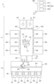
- FIG. 1 is a plan view showing an outline of a configuration of a plasma processing system as a substrate processing system according to an embodiment of the present invention.
- FIG. 2 is a diagram showing an outline of the configuration of a transport robot provided in a transfer module.
- FIG. 2 is a vertical cross-sectional view showing an outline of the configuration of a processing module.
- FIG. 4 is a partially enlarged view of FIG. 3 .
- 5 is an enlarged cross-sectional view of a portion different from FIG. 4 in the circumferential direction of the wafer support table.
- 11 is a flowchart showing an example 1 of an edge ring attachment sequence.
- 11A and 11B are diagrams illustrating the state of the processing module when an edge ring attachment sequence is executed.
- 11A and 11B are diagrams illustrating the state of the processing module when an edge ring attachment sequence is executed.
- 11A and 11B are diagrams illustrating the state of the processing module when an edge ring attachment sequence is executed.
- 11A and 11B are diagrams illustrating the state of the processing module when an edge ring attachment sequence is executed.
- 11A and 11B are diagrams illustrating the state of the processing module when an edge ring attachment sequence is executed.
- 11A and 11B are diagrams illustrating the state of the processing module when an edge ring attachment sequence is performed.
- 11A and 11B are diagrams illustrating the state of the processing module when an edge ring attachment sequence is executed.
- 11A and 11B are diagrams illustrating the state of the processing module when an edge ring attachment sequence is executed.
- 11 is a flowchart showing an example 3 of an edge ring attachment sequence.
- 10 is a flowchart showing an example 5 of an edge ring attachment sequence.
- 13 is a flowchart showing an example 7 of an edge ring attachment sequence.
- 13 is a flowchart showing an example 8 of an edge ring attachment sequence.
- 1 is a partial enlarged view for explaining an example of a wafer support stage configured to mount a cover ring in addition to an edge ring;
- 13 is a partial enlarged view for explaining another example of a wafer support table configured to mount a cover ring in addition to an edge ring.
- FIG. FIG. 13 is a partial enlarged view for explaining another example of the electrostatic chuck.
- substrate processing such as etching using plasma, i.e. plasma processing
- plasma processing is performed on substrates such as semiconductor wafers (hereafter referred to as "wafers").
- substrates such as semiconductor wafers (hereafter referred to as "wafers").
- Plasma processing is performed with the substrate placed on a substrate support table inside a reduced pressure processing chamber.
- a ring-shaped member in a planar view known as a focus ring, edge ring, etc. (hereinafter referred to as an "edge ring”) may be placed on the substrate support table so as to surround the periphery of the substrate on the substrate support table.
- the temperature of the substrate support table is adjusted, and the temperature of the substrate is adjusted via the substrate support table.
- the temperature of the edge ring is also important because the temperature of the edge ring affects the plasma processing result of the peripheral portion of the substrate. Therefore, the temperature of the edge ring is also adjusted via the substrate support table.
- an electrostatic chuck is provided on the substrate support stand, and the substrate and edge ring are electrostatically attracted to the electrostatic chuck.
- edge ring is etched and worn out by exposure to plasma, making it necessary to replace it.
- the edge ring becomes worn out, it is generally replaced by an operator with the processing vessel open to the atmosphere, but it is also being considered to replace the edge ring without opening the processing vessel to the atmosphere by using a transport device to transport the edge ring (see Patent Document 1).
- the edge ring When using an edge ring, the edge ring must be appropriately positioned relative to the substrate support table so that uniform processing results can be obtained around the edge of the substrate. Specifically, for example, the center of the electrostatic chuck and the center of the edge ring must be positioned approximately the same.
- the edge ring when the edge ring is placed on the electrostatic chuck of the substrate support stand using a transport device for transporting the edge ring, the position of the edge ring relative to the substrate support stand may become inappropriate. Even if the edge ring is appropriate when it is placed on the substrate, the position of the edge ring relative to the substrate support stand may shift and become inappropriate when electrostatically attracted.
- the technology disclosed herein places the edge ring on the substrate support with high precision.
- Fig. 1 is a plan view showing an outline of the configuration of a plasma processing system as a substrate processing system according to the present embodiment
- Fig. 2 is a view showing an outline of the configuration of a transfer robot provided in a transfer module described later.
- substrate processing such as an etching process using plasma, that is, plasma processing.
- the plasma processing system 1 has an atmospheric section 10 and a reduced pressure section 11, which are connected together via load lock modules 20, 21.
- the atmospheric section 10 includes an atmospheric module that performs a desired process on the wafer W in an atmospheric pressure environment.
- the reduced pressure section 11 includes a reduced pressure module that performs a desired process on the wafer W in a reduced pressure atmosphere (vacuum atmosphere).
- the load lock modules 20 and 21 are provided to connect the loader module 30 included in the atmospheric section 10 and the transfer module 50 included in the reduced pressure section 11 via a gate valve (not shown).
- the load lock modules 20 and 21 are configured to temporarily hold the wafer W.
- the load lock modules 20 and 21 are also configured so that their interiors can be switched between atmospheric pressure and reduced pressure atmospheres.
- the atmospheric section 10 has a loader module 30 equipped with a transport mechanism 40 described below, and a load port 32 on which a FOUP 31 is placed.
- the FOUP 31 is capable of storing multiple wafers W.
- the loader module 30 may also be connected to an orienter module (not shown) that adjusts the horizontal orientation of the wafer W, a buffer module (not shown) that temporarily stores multiple wafers W, and the like.
- the loader module 30 has a rectangular housing, and the interior of the housing is maintained at atmospheric pressure.
- Multiple load ports 32 for example five load ports 32, are arranged side by side on one side that constitutes the long side of the loader module 30 housing.
- Load lock modules 20 and 21 are arranged side by side on the other side that constitutes the long side of the loader module 30 housing.
- a transport mechanism 40 configured to hold and transport a wafer W is provided inside the housing of the loader module 30.
- the transport mechanism 40 has a transport arm 41 that supports the wafer W during transport, a rotating table 42 that rotatably supports the transport arm 41, and a base 43 on which the rotating table 42 is mounted.
- a guide rail 44 is provided inside the loader module 30, extending in the longitudinal direction of the loader module 30.
- the base 43 is provided on the guide rail 44, and the transport mechanism 40 is configured to be movable along the guide rail 44.
- the decompression section 11 has a transfer module 50 as a decompression transport device, a processing module 60 as a plasma processing device, and a storage module 61 as a storage section.
- the insides of the transfer module 50 and the processing module 60 (specifically, the insides of the decompression transport chamber 51 and the chamber 100 described below) are each maintained in a decompression atmosphere, and the inside of the storage module 61 is also maintained in a decompression atmosphere.
- multiple processing modules 60 for example six, are provided, and multiple storage modules 61, for example two, are also provided.
- the number and arrangement of the processing modules 60 are not limited to this embodiment and can be set arbitrarily, as long as at least one processing module equipped with a wafer support table described below is provided.
- the number and arrangement of the storage modules 61 are not limited to this embodiment and can be set arbitrarily, for example at least one is provided.
- the transfer module 50 is configured to transport therein a wafer W.
- the transfer module 50 is also configured to transport therein an edge ring E, which will be described later.
- the transfer module 50 includes a reduced pressure transfer chamber 51 having a housing having a polygonal shape when viewed from above (a rectangular shape when viewed from above in the illustrated example), and the reduced pressure transfer chamber 51 is connected to the load lock modules 20 and 21 .
- the transfer module 50 transfers the wafer W that has been loaded into the load lock module 20 to one of the processing modules 60 , and also unloads the wafer W that has been subjected to the desired plasma processing in the processing module 60 to the load lock module 21 .
- the transfer module 50 may transport the edge ring E in the storage module 61 to one of the processing modules 60 and may also unload the edge ring E in the processing module 60 to the storage module 61 .
- the processing module 60 performs a desired plasma process, such as an etching process, on the wafer W transferred from the transfer module 50.
- the processing module 60 is also connected to the transfer module 50 via a gate valve 62. The specific configuration of the processing module 60 will be described later.
- the storage module 61 stores the edge ring E.
- the storage module 61 is also connected to the transfer module 50 via a gate valve 63.
- a transfer robot 70 is provided inside the reduced pressure transfer chamber 51 of the transfer module 50.
- the transfer robot 70 is configured to be capable of holding and transferring a wafer W.
- the transfer robot 70 is also configured to be capable of holding and transferring an edge ring E.
- the transport robot 70 has a transport arm 71 that is configured to be able to rotate, extend, and move up and down freely while holding a wafer W.
- the tip of the transport arm 71 branches into forks 72, 72 that serve as two holding parts.
- Each of the forks 72, 72 is configured to be able to hold the wafer W and edge ring E to be transported.
- at least one of the forks 72, 72 may be provided with a measuring part 73.
- the measuring part 73 measures information regarding the amount of positional deviation of the edge ring E relative to an electrostatic chuck (described below) that is provided in the processing module 60.
- the measuring part 73 has, for example, a distance sensor (not shown).
- the transfer arm 71 receives the wafer W held in the load lock module 20 and transports it into the processing module 60.
- the transfer arm 71 also receives the wafer W that has been subjected to the desired processing in the processing module 60 and transports it to the load lock module 21.
- the transport arm 71 may receive the edge ring E in the storage module 61 and transport it into the processing module 60.Furthermore, in the transfer module 50, the transport arm 71 may receive the edge ring E in the processing module 60 and transport it out to the storage module 61.
- the plasma processing system 1 includes a controller 80.
- the controller 80 processes computer executable instructions that cause the plasma processing system 1 to perform the various steps described in this disclosure.
- the controller 80 may be configured to control each of the other elements of the plasma processing system 1 such that the plasma processing system 1 performs the various steps described herein.
- some or all of the controller 80 may be included in the other elements of the plasma processing system 1.
- the controller 80 may include, for example, a computer 90.
- the computer 90 may include, for example, a processing unit (CPU: Central Processing Unit) 91, a memory unit 92, and a communication interface 93.
- the processing unit 91 may be configured to perform various control operations and calculations based on programs stored in the memory unit 92.
- the memory unit 92 may include a random access memory (RAM), a read only memory (ROM), a hard disk drive (HDD), a solid state drive (SSD), or a combination thereof.
- the communication interface 93 may communicate with other elements of the plasma processing system 1 via a communication line such as a LAN (Local Area Network).
- LAN Local Area Network
- the transfer mechanism 40 removes the wafer W from the desired FOUP 31 and loads it into the load lock module 20.
- the inside of the load lock module 20 is sealed and depressurized. After that, the inside of the load lock module 20 and the inside of the transfer module 50 are connected to each other.
- the wafer W is then held by the transfer robot 70 and transported from the load lock module 20 to the transfer module 50.
- the gate valve 62 corresponding to the desired processing module 60 is opened, and the transfer robot 70 loads the wafer W into the desired processing module 60.
- the gate valve 62 is then closed, and the desired processing is performed on the wafer W in the processing module 60.
- the processing performed on the wafer W in this processing module 60 will be described later.
- the gate valve 62 is opened, and the wafer W is removed from the processing module 60 by the transfer robot 70. After that, the gate valve 62 is closed.
- the wafer W is loaded into the load lock module 21 by the transfer robot 70.
- the inside of the load lock module 21 is sealed and opened to the atmosphere. After that, the inside of the load lock module 21 and the inside of the loader module 30 are connected to each other.
- the wafer W is held by the transfer mechanism 40 and returned from the load lock module 21 via the loader module 30 to the desired FOUP 31 where it is stored. This completes the wafer processing using the plasma processing system 1.
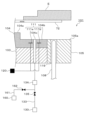
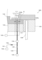
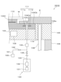
- Fig. 3 is a vertical cross-sectional view showing an outline of the configuration of the processing module 60.
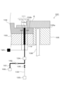
- Fig. 4 is a partially enlarged view of Fig. 3.
- Fig. 5 is an enlarged cross-sectional view of a portion different from Fig. 4 in the circumferential direction of the wafer support table 101 described below.
- the processing module 60 includes a chamber 100 as a processing vessel, a gas supply unit 140, an RF (Radio Frequency) power supply unit 150, and an exhaust system 160.
- the processing module 60 also includes a voltage application unit 120 (see FIG. 4) and a gas supply unit 130 (see FIG. 5).
- the processing module 60 includes a wafer support table 101 as a substrate support table, and an upper electrode 102.
- the chamber 100 is configured so that its interior can be depressurized, and defines a processing space 100s in which plasma is generated.
- the chamber 100 also has a wafer support 101 and other components provided inside.
- the chamber 100 can be made of a material such as aluminum.
- the chamber 100 is also connected to a ground potential.
- the wafer support 101 is disposed, for example, in a lower region within the chamber 100.
- the upper electrode 102 is disposed above the wafer support 101 and can function as part of the ceiling of the chamber 100.
- the wafer support table 101 is configured to support a wafer W.
- the wafer support table 101 includes a lower electrode 103, an electrostatic chuck 104, a support 105, an insulator 106, a lifter 107, and a lifter 108.
- the wafer support table 101 is also configured to support an edge ring E.
- the wafer support table 101 may or may not include an edge ring E as a component thereof.
- the lower electrode 103 is formed of a conductive material such as aluminum.
- a flow path 109 for a temperature control fluid is formed inside the lower electrode 103.
- the temperature control fluid is supplied to the flow path 109 from a chiller unit (not shown) provided outside the chamber 100.
- the temperature control fluid supplied to the flow path 109 is returned to the chiller unit.
- the wafer support table 101 specifically, the electrostatic chuck 104
- the wafer W, or the edge ring E can be cooled to a predetermined temperature by circulating, for example, low-temperature brine as a temperature control fluid in the flow path 109.
- the wafer support table 101 (specifically, the electrostatic chuck 104), the wafer W, or the edge ring E can be heated to a predetermined temperature by circulating, for example, high-temperature brine as a temperature control fluid in the flow path 109.
- the form of the temperature control mechanism is not limited to the above-mentioned flow path 109, and may be another form, such as a resistance heating heater.
- the member on the wafer support table 101 on which the temperature control mechanism is provided is not limited to the lower electrode 103, and may be another member.
- the electrostatic chuck 104 is a member configured to be able to electrostatically attract at least the edge ring E, and is provided on the lower electrode 103.
- the electrostatic chuck 104 may also be configured to be able to electrostatically attract the wafer W.
- the center of the electrostatic chuck 104 constitutes a substrate mounting portion.
- the top surface of the central portion of the electrostatic chuck 104 is higher than the top surface of the peripheral portion.
- the wafer W is mounted on the top surface 104a of the central portion of the electrostatic chuck 104
- the edge ring E is mounted on the top surface 104b of the peripheral portion of the electrostatic chuck 104.
- the top surface 104a of the central portion of the electrostatic chuck 104 serves as a wafer mounting surface on which the wafer W is mounted
- the top surface 104b of the peripheral portion of the electrostatic chuck 104 serves as a ring mounting surface on which the edge ring E is mounted so as to surround the substrate mounting surface
- the edge ring E is a member arranged to surround the wafer W, specifically, a member arranged to surround the wafer W placed on the electrostatic chuck 104. In one embodiment, the edge ring E is arranged to surround a central portion of the electrostatic chuck 104, the upper surface of which is higher than the peripheral portion.
- the edge ring E is formed in a circular ring shape in a plan view.
- the edge ring E is made of a material such as Si, SiO2 , or the like.
- An electrode 110 for electrostatically attracting the wafer W to an upper surface 104a of the central portion may be provided in the electrostatic chuck 104.
- An electrode 111 for electrostatically attracting the edge ring E to an upper surface 104b of the peripheral portion is provided in the electrostatic chuck 104.
- the electrode 111 is, for example, a bipolar type including a pair of electrodes 111a, 111b formed at different positions from each other.
- the electrostatic chuck 104 has a configuration in which electrodes 110 and 111 are sandwiched between insulating materials made of, for example, an insulating material.
- a voltage application unit 120 is connected to the electrode 111 so as to generate an electrical force (specifically, for example, Coulomb force) for electrostatically adsorbing the edge ring E.
- an electrical force specifically, for example, Coulomb force
- the electrode 111 is a bipolar type, it is configured so that the voltage application unit 120 can selectively apply either voltages of opposite polarities or voltages of the same polarity to the pair of electrodes 111a, 111b.
- the voltage application unit 120 includes, for example, two DC power sources 121a and 121b and two switches 122a and 122b.
- the DC power supply 121a is connected to the electrode 111a via the switch 122a, and selectively applies a positive voltage or a negative voltage for electrostatically attracting the edge ring E to the electrode 111a.
- the DC power supply 121b is connected to the electrode 111b via a switch 122b, and selectively applies a positive voltage or a negative voltage for electrostatically attracting the edge ring E to the electrode 111b.
- the voltage application unit 120 may include a DC power supply 121c and a switch 122c.
- the DC power supply 121c is connected to the electrode 110 via a switch 122c, and applies a voltage to the electrode 110 for electrostatically attracting the wafer W thereto.
- the central portion of the electrostatic chuck 104 where the electrode 110 is provided and the peripheral portion where the electrode 111 is provided are integrated, but these central portion and peripheral portion may be separate.
- the electrode 111 for attracting and holding the edge ring E is a bipolar type, but it may be a unipolar type.
- the central portion of the electrostatic chuck 104 is formed, for example, with a diameter smaller than the diameter of the wafer W, so that when the wafer W is placed on the upper surface 104a of the central portion of the electrostatic chuck 104, the peripheral portion of the wafer W protrudes from the central portion of the electrostatic chuck 104.
- the edge ring E has a step formed on its upper portion, and the upper surface of the outer periphery is higher than the upper surface of the inner periphery.
- the inner periphery of the edge ring E is formed to be recessed under the peripheral edge of the wafer W that protrudes from the center of the electrostatic chuck 104. In other words, the inner diameter of the edge ring E is smaller than the outer diameter of the wafer W.
- the support 105 is a member formed in a ring shape in a plan view using an insulating material such as quartz, and is arranged to surround the lower electrode 103 and the electrostatic chuck 104.
- the electrostatic chuck 104 may have a gas discharge hole (not shown) formed in the central upper surface 104a for discharging a heat transfer gas into the gap between the back surface of the placed wafer W and the wafer W.
- a heat transfer gas is supplied from the gas discharge hole from a gas supply unit (not shown).
- the gas supply unit may include one or more gas sources and one or more pressure controllers. In one embodiment, the gas supply unit is configured to supply the heat transfer gas from the gas source to the gas supply hole via a pressure controller, for example.
- gas discharge holes 104c are formed in the upper surface 104b of the peripheral portion of the electrostatic chuck 104. Specifically, one end of the gas discharge hole 104c is open in the upper surface 104b of the peripheral portion of the electrostatic chuck 104. For example, a plurality of gas discharge holes 104c are provided along the circumferential direction of the electrostatic chuck 104. The gas discharge holes 104c supply a heat transfer gas such as helium gas to a gap between the back surface of the edge ring E placed on the upper surface 104b of the peripheral portion of the electrostatic chuck 104 and the upper surface 104b.
- a heat transfer gas such as helium gas
- the gas supply unit 130 may include one or more gas sources 131 and one or more flow rate controllers 132.
- the gas supply unit 130 is configured to supply, for example, a heat transfer gas from a gas source 131 through a flow rate controller 132 to the gas discharge holes 104c.
- Each flow rate controller 132 may include, for example, a mass flow controller or a pressure-controlled flow rate controller.
- the gas discharge holes 104c and the piping 1333 may function as at least a part of a supply path that supplies gas between the upper surface 104b of the peripheral portion of the electrostatic chuck 104, which is the ring mounting surface, and the back surface of the edge ring E.
- the end of the gas discharge hole 104c opposite the upper surface 104b of the peripheral portion is connected to the exhaust system 160 via the piping 161. This allows the periphery of the upper surface 104b of the peripheral portion of the electrostatic chuck 104 to be exhausted via the gas discharge hole 104c. That is, the gas discharge hole 104c can function as an exhaust hole that exhausts the periphery of the ring mounting surface including the upper surface 104b of the peripheral portion of the electrostatic chuck 104.
- the gas discharge hole 104c and the piping 161 can function as at least a part of an exhaust path that exhausts the space between the upper surface 104b of the peripheral portion of the electrostatic chuck 104, which is the ring mounting surface, and the back surface of the edge ring E.
- a pressure sensor 134 for measuring the pressure in the above-mentioned supply path is provided for the electrostatic chuck 104 in order to measure the pressure in the gap between the edge ring E electrostatically attracted to the upper surface 104b of the peripheral portion and the above-mentioned upper surface 104b.
- the pressure sensor 134 is provided in the pipe 133, for example.
- the pipe 133 may be provided with a switching valve 135 for switching between on and off the supply of the heat transfer gas by the gas supply unit 130.
- the pipe 161 may be provided with a switching valve 162 for switching between on and off the exhaust of the periphery of the upper surface 104b of the peripheral portion by the exhaust system 160.
- the insulator 106 in FIG. 3 is a cylindrical member made of ceramic or the like, and supports the support 105.
- the insulator 106 is formed, for example, to have an outer diameter equal to the outer diameter of the support 105, and supports the peripheral portion of the support 105.
- the lifter 107 is a member that moves up and down relative to the upper surface 104a at the center of the electrostatic chuck 104, and is formed, for example, in a columnar shape using a ceramic material. When the lifter 107 moves up, its upper end protrudes from the upper surface 104a, and the lifter 107 is capable of supporting the wafer W.
- the lifter 107 allows the wafer W to be transferred between the wafer support table 101 and the transfer arm 71 of the transfer robot 70.
- Three or more lifters 107 are provided at intervals from one another and extend in the vertical direction.
- the lifters 107 are raised and lowered by an actuator 112.
- the actuator 112 has, for example, a support member 113 that supports the multiple lifters 107, and a drive unit 114 that generates a driving force to raise and lower the support member 113 and raise and lower the multiple lifters 107.
- the drive unit 114 has, for example, a motor (not shown) as a driving source that generates the driving force.
- the lifter 107 is inserted into an insertion hole 115 whose upper end opens into the upper surface 104a of the central portion of the electrostatic chuck 104.
- the insertion hole 115 is formed, for example, to extend downward from the upper surface 104a of the central portion of the electrostatic chuck 104 to the bottom surface of the lower electrode 103.
- the lifter 108 is a lifting member that moves up and down relative to the upper surface 104b of the peripheral portion of the electrostatic chuck 104, and is made of, for example, ceramic.
- the lifter 108 is formed, for example, in a columnar shape except for the upper end (i.e., the tip), which is formed in a hemispherical shape.
- the lifter 108 is configured so that the upper end thereof can protrude from the upper surface 105a of the support 105 when raised.
- Three or more lifters 108 are provided at intervals along the circumferential direction of the electrostatic chuck 104, and extend in the vertical direction.
- the lifter 108 is raised and lowered by an actuator 116.
- the actuator 116 has, for example, a support member 117 provided for each lifter 108, which supports the lifter 108 so that it can move horizontally.
- the support member 117 has, for example, a thrust bearing, to support the lifter 108 so that it can move horizontally.
- the actuator 116 also has a drive unit 118 that generates a driving force to raise and lower the support member 117 and raise and lower the lifter 108.
- the drive unit 118 has, for example, a motor (not shown) as a driving source that generates the driving force.
- the lifter 108 is inserted into an insertion hole 119 whose upper end opens into the upper surface 105a of the support 105.
- the insertion hole 119 is formed, for example, to penetrate the support 105 in the vertical direction.
- the edge ring E can be transferred between the wafer support table 101 and the transfer arm 71 of the transfer robot 70 by the lifter 108 as described above.
- the lifter 108 and the actuator 116 form a lifting mechanism that raises and lowers the edge ring E relative to the ring mounting surface.
- the upper electrode 102 also functions as a gas supply or showerhead that delivers one or more gases from the gas supply 140 into the chamber 100.
- the upper electrode 102 has a gas inlet 102a, a gas diffusion chamber 102b, and a number of gas outlets 102c.
- the gas inlet 102a is, for example, in fluid communication with the gas supply 140 and the gas diffusion chamber 102b.
- the number of gas outlets 102c are in fluid communication with the gas diffusion chamber 102b and the interior of the chamber 100.
- the upper electrode 102 is configured to deliver a gas, such as one or more process gases, from the gas inlet 102a through the gas diffusion chamber 102b and the number of gas outlets 102c into the chamber 100.
- the gas supply 140 may include one or more gas sources 141 and one or more flow controllers 142.
- the gas supply 140 is configured to supply, for example, one or more gases from a respective gas source 141 to the gas inlet 102a via a respective flow controller 142.
- Each flow controller 142 may include, for example, a mass flow controller or a pressure-controlled flow controller.
- the gas supply 140 may include one or more flow modulation devices to modulate or pulse the flow rate of one or more gases.
- the RF power supply 150 is configured to supply RF power, e.g., one or more RF signals, to one or more electrodes, such as the lower electrode 103, the upper electrode 102, or both the lower electrode 103 and the upper electrode 102. This generates a plasma from one or more process gases supplied in the chamber 100, i.e., the processing space 100s.
- the RF power supply 150 can function as at least a part of a plasma generating unit that generates plasma in the chamber 100.
- the plasma generating unit is specifically configured to generate plasma from one or more gases in the chamber 100.
- the RF power supply 150 includes, for example, two RF generating units 151a, 151b and two matching circuits 152a, 152b.
- the RF power supply 150 is configured to supply a first RF signal from the first RF generating unit 151a to the lower electrode 103 via the first matching circuit 152a.
- the first RF signal may have a frequency in the range of 27 MHz to 100 MHz.
- the RF power supply unit 150 is configured to supply a second RF signal from the second RF generating unit 151b to the lower electrode 103 via the second matching circuit 152b.
- the second RF signal may have a frequency in the range of 400 kHz to 13.56 MHz.
- a DC (Direct Current) pulse generating unit may be used in place of the second RF generating unit 151b.
- the RF power supply 150 may be configured to supply a first RF signal from an RF generator to the lower electrode 103, a second RF signal from another RF generator to the lower electrode 103, and a third RF signal from yet another RF generator to the lower electrode 103.
- a DC voltage may be applied to the upper electrode 102.
- one or more RF signals may be pulsed or modulated in amplitude.
- Amplitude modulation may include pulsing the RF signal amplitude between an on state and an off state, or between two or more different on states.
- the exhaust system 160 may be connected to an exhaust port 100e provided at the bottom of the chamber 100, for example.
- the exhaust system 160 may include a pressure valve and a vacuum pump.
- the vacuum pump may include a turbomolecular pump, a roughing pump, or a combination thereof.
- ⁇ Wafer Processing in Processing Module 60 Next, a description will be given of an example of wafer processing performed using the processing module 60.
- a plasma processing such as an etching process is performed on the wafer W.
- the wafer W is loaded into the chamber 100 by the transfer robot 70, and the lifter 107 is raised and lowered to place the wafer W on the electrostatic chuck 104.
- a DC voltage is then applied from the DC power supply 121c to the electrode 110 of the electrostatic chuck 104, so that the wafer W is electrostatically attracted to and held on the electrostatic chuck 104.
- the exhaust system 160 reduces the pressure inside the chamber 100 to a predetermined vacuum level.
- a processing gas is supplied from the gas supply unit 140 to the processing space 100s via the upper electrode 102.
- high frequency power HF for plasma generation is supplied from the RF power supply unit 150 to the lower electrode 103, which excites the processing gas and generates plasma.
- high frequency power LF for ion attraction may also be supplied from the RF power supply unit 150. Then, plasma processing is performed on the wafer W by the action of the generated plasma.
- a DC voltage is applied from DC power sources 121a and 121b to electrode 111 of electrostatic chuck 104, whereby edge ring E is electrostatically attracted and held on electrostatic chuck 104.
- a heat transfer gas is discharged via gas supply unit 130 or the like toward the bottom surfaces of wafer W and edge ring E attracted and held on electrostatic chuck 104.
- the supply of high frequency power HF from the RF power supply unit 150 and the supply of processing gas from the gas supply unit 140 are stopped. If high frequency power LF was being supplied during plasma processing, the supply of the high frequency power LF is also stopped. Next, the adsorption and holding of the wafer W by the electrostatic chuck 104 is stopped. In addition, the supply of heat transfer gas to the bottom surface of the wafer W may be stopped.
- the wafer W is raised by the lifter 107 and detached from the electrostatic chuck 104.
- a de-electrification process may be performed on the wafer W.
- the transfer robot 70 removes the wafer W from the chamber 100, completing the series of wafer processing steps.
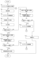
- FIG. 6 is a flow chart showing an example 1 of the sequence for attaching the edge ring E.
- FIGS. 7 to 14 are schematic diagrams showing the state of the processing module 60 when the sequence for attaching the edge ring E is executed.
- the valve in the open state and the voltage application unit 120 in the ON state are painted white
- the valve in the closed state and the voltage application unit 120 in the OFF state are painted black
- the pipe through which the gas flows is shown in thick lines.
- the gas discharge hole 104c in a state in which exhaust is performed through the gas discharge hole 104c is shown in black
- the gas discharge hole 104c in a state in which the heat transfer gas exists therein is shown in gray
- the gas discharge hole 104c in other states is shown in white. Note that the following steps are executed by the plasma processing system 1 according to the control and calculation of the control device 80 (specifically, the processing unit 91) based on the program stored in the storage unit 92.
- step S1 the edge ring E is transported into the chamber 100 by the transport robot 70 and handed over to the lifting mechanism including the lifter 108, and is then lowered by the lifting mechanism and placed on the ring placement surface (step S1).
- This step S1 is performed in a state where no wafer W is present in the chamber 100.
- step S1 for example, the edge ring E in the storage module 61 is first transferred by the transfer robot 70 into the chamber 100 of the processing module 60 to which the edge ring E is to be attached.
- the edge ring E in the storage module 61 is held by the fork 72 of the transfer arm 71 of the transfer robot 70.
- the chamber 100 is evacuated by the exhaust system 160 without gas being discharged through the upper electrode 102, and the chamber 100 is made into a high vacuum.
- the corresponding gate valve 62 is opened, and the fork 72 holding the edge ring E is inserted into the chamber 100 through a loading/unloading port (not shown).
- the edge ring E is transferred by the fork 72 above the upper surface 104b of the peripheral portion of the electrostatic chuck 104 and the upper surface 105a of the support 105.
- the wafer W is not placed on the upper surface 104a of the central portion of the electrostatic chuck 104.
- the edge ring E is transferred from the transfer robot 70 to the lifter 108 . Specifically, all the lifters 108 are raised, and the edge ring E is transferred from the forks 72 to the lifters 108, as shown in Fig. 8. Thereafter, the forks 72 are removed from the chamber 100, and the gate valve 62 is closed.
- the edge ring E is lowered by a lifting mechanism including a lifter 108 and placed on the upper surface 104b of the peripheral portion of the electrostatic chuck 104, which is the ring mounting surface. Specifically, the lifter 108 is lowered until the upper end of the lifter 108 fits into the insertion hole 119. As a result, the edge ring E is placed on the upper surface 104b of the peripheral portion of the electrostatic chuck 104, which is the ring placement surface, as shown in FIG.
- the edge ring E is vacuum-adsorbed onto the ring mounting surface (step S2). Specifically, in a state in which no wafer W is present in the chamber 100, the periphery of the ring mounting surface is evacuated via the gas ejection holes 104c, which also function as exhaust holes. 10, the switching valve 162 is opened, and the exhaust system 160 exhausts air from the periphery of the upper surface 104b of the electrostatic chuck 104 and the periphery of the upper surface 105a of the support 105 through the gas discharge holes 104c. In particular, the vicinity of the upper surface 104b of the peripheral portion of the electrostatic chuck 104 is exhausted through the gas discharge holes 104c. As a result, the edge ring E is vacuum-attached to the upper surface 104b of the peripheral portion of the electrostatic chuck 104, which is the ring mounting surface.
- the placed edge ring E is electrostatically attracted to the ring mounting surface (step S3). Specifically, in a state where no wafer W is present in the chamber 100, the edge ring E is placed on the ring mounting surface, and exhaust is being performed via the gas ejection holes 104c, a voltage is applied to the electrode 111 of the electrostatic chuck 104. 11 , in a state where an edge ring E is placed on an upper surface 104b of the peripheral portion of the electrostatic chuck 104, which is a ring mounting surface, and exhaust is being performed via the gas discharge holes 104c, the voltage application unit 120 is turned on, specifically, the DC power supplies 121a and 121b are turned on.
- a DC voltage is applied to the electrode 111 of the electrostatic chuck 104.
- DC voltages having mutually opposite polarities are applied to the electrodes 111a and 111b.
- a voltage may be applied to the electrode 111 of the electrostatic chuck 104 while the exhaust is stopped.
- step S4 gas is supplied to the supply passage including the gas ejection holes 104c so that the pressure in the supply passage is maintained higher than the pressure in the chamber 100 (step S4). Specifically, when no wafer W is present in the chamber 100, exhaust through the gas discharge holes 104c is stopped, and a predetermined gas is discharged through the gas discharge holes 104c into the gap between the ring mounting surface and the edge ring E, so that the pressure in the gap is made higher than the pressure in the chamber 100. At the end of step S4, the supply of gas to the supply path, that is, the discharge of the predetermined gas from the gas discharge hole 104c, is stopped.
- step S4 the switching valve 162 is closed and exhaust through the gas discharge hole 104c by the exhaust system 160 is stopped.
- the switching valve 135 is opened and the heat transfer gas supplied from the gas supply unit 130 is discharged into the gap through the gas discharge hole 104c.
- the target pressure is, for example, the pressure in the gap during plasma processing.
- step S5 After the gas is supplied in step S4, the pressure in the supply path including the gas ejection holes 104c is measured (step S5).
- step S5 specifically, after a predetermined time has elapsed since the gas supply was stopped in step S4, the pressure in pipe 133 (more specifically, the pressure downstream of switching valve 135 of pipe 133) is measured by pressure sensor 134.
- the predetermined time is, for example, 10 to 100 seconds, and this information is stored in memory unit 92 in advance.
- the pressure downstream of the switching valve 135 of the pipe 133 is approximately equal to the pressure in the gap between the ring mounting surface and the edge ring E. Therefore, step S5 can be rephrased as a process of measuring the pressure in the gap between the ring mounting surface and the edge ring E.
- the control device 80 judges the mounting state of the edge ring E on the ring mounting surface based on the measurement result in step S5, that is, judges whether the mounting state is proper or not (step S6). Specifically, the control device 80 determines whether or not the predetermined gas is leaking from the gap based on the measurement result in step S5. More specifically, the control device 80 determines whether or not the pressure measured in step S5 is less than a threshold value in order to determine whether or not the predetermined gas is leaking from the gap. This threshold value is set to, for example, 90% to 98% of the target pressure, and the information on this is stored in advance in the storage unit 92.
- step S6 if it is determined that the mounting condition of the edge ring E on the ring mounting surface is not appropriate, i.e., if it is determined that a specified gas is leaking from the above-mentioned gap (NO), information regarding the amount of positional deviation of the edge ring E relative to the electrostatic chuck 104 is measured by the measuring unit 73 of the transport robot 70. Specifically, when it is determined that a predetermined gas is leaking from the gap, that is, when the pressure measured in step S5 is less than the threshold value, first, the gate valve 62 is opened, and the fork 72 not holding the wafer W and the edge ring E is inserted into the chamber 100.
- the distance sensor included in the measuring unit 73 measures the distance from the distance sensor to the wafer support table 101 at predetermined intervals in the circumferential direction of the electrostatic chuck 104 and at predetermined minute intervals in the radial direction of the electrostatic chuck 104.
- the control device 80 calculates the amount of positional deviation of the edge ring E with respect to the electrostatic chuck 104 based on the measurement result by the measuring unit 73 (step S8). Specifically, the control device 80 identifies the peripheral edge of the central portion of the electrostatic chuck 104 and the inner peripheral edge of the edge ring E at predetermined intervals in the circumferential direction of the electrostatic chuck 104 from the measurement result in step S7, and calculates the distance from the peripheral edge of the central portion of the electrostatic chuck 104 to the inner peripheral edge of the edge ring E.
- control device 80 calculates the amount of positional deviation of the edge ring E relative to the electrostatic chuck 104 (specifically, the distance from the center of the central portion of the electrostatic chuck 104 to the center of the edge ring E) based on the calculation results at the predetermined intervals.
- the amount of positional deviation calculated here also includes the direction of the positional deviation.
- control device 80 determines whether the amount of positional deviation calculated in step S8 exceeds a threshold value (step S9).
- This threshold value is, for example, 200 ⁇ m, and this information is stored in advance in the storage unit 92.
- step S9 If it is determined in step S9 that the amount of positional deviation exceeds the threshold (YES), the position of the edge ring E on the ring mounting surface is adjusted (step S10).
- the application of voltage to the electrode 111 of the electrostatic chuck 104 is stopped, and the edge ring E is raised by the lifting mechanism including the lifter 108, and then the edge ring E is transferred to the transfer robot 70. More specifically, the application of DC voltage from the voltage application unit 120 to the electrode 111 is stopped, and the fork 72 of the transfer robot 70 is retracted from above the wafer support table 101. Next, the edge ring E is de-electrified, and then all the lifters 108 are raised, and the edge ring E is transferred from the wafer support table 101 to the lifters 108. Next, the fork 72 of the transfer arm 71 is moved between the wafer support table 101 and the edge ring E supported by the lifters 108. Next, all the lifters 108 are lowered, and the edge ring E is transferred from the lifters 108 to the forks 72.
- the edge ring E is moved to a position based on the amount of positional deviation calculated in step S8.
- the fork 72 is moved to a corrected position based on the amount of positional deviation calculated in step S8.
- the corrected position is calculated in advance by the control device 80 from the amount of positional deviation calculated in step S8 so that the amount of positional deviation approaches zero.
- edge ring E is returned to the lifting mechanism including the lifter 108, and the edge ring E is lowered by the lifting mechanism and placed again on the ring placement surface.
- the edge ring E is transferred from the forks 72 to the lifters 108.
- the forks 72 are removed from the chamber 100, and the gate valve 62 is closed.
- the edge ring E is lowered by a lifting mechanism including a lifter 108 and placed on the upper surface 104b of the peripheral portion of the electrostatic chuck 104, which is the ring mounting surface.
- the lifter 108 is lowered until the upper end of the lifter 108 fits into the insertion hole 119.
- the edge ring E is placed on the upper surface 104b of the peripheral portion of the electrostatic chuck 104, which is the ring placement surface.
- step S10 the sequence returns to step S2, where the edge ring E is vacuum-adsorbed, etc.
- step S6 if it is determined that the mounting state of the edge ring E on the edge ring mounting surface is appropriate, that is, if it is determined that no leakage of a predetermined gas is occurring from the gap (specifically, if the pressure in the gap measured in step S5 is equal to or greater than a threshold value) (YES), step S11, which is similar to step S7, is performed. As a result, information regarding the amount of positional deviation of the edge ring E relative to the electrostatic chuck 104 is measured by the measurement unit 73.
- control device 80 calculates the amount of positional deviation of the edge ring E relative to the electrostatic chuck 104 based on the measurement results from the measurement unit 73 (step S12).
- control device 80 determines whether the position deviation amount calculated in step S13 is equal to or less than a threshold value (step S13).
- step S14 a process for stabilizing the electrostatic attraction of the edge ring E is performed (step S14). Specifically, for example, plasma of the processing gas is generated in the chamber 100, and the charged state of the edge ring E is changed by the plasma, thereby strengthening the electrostatic adsorption force of the edge ring E. This completes the sequence.
- step S13 determines whether the amount of positional deviation exceeds the threshold value (NO)
- step S16 the position of the edge ring E on the ring mounting surface is adjusted (step S16) in the same manner as in step S10, with no wafer W present in the chamber 100.
- step S16 the sequence returns to step S2, and the edge ring E is vacuum-adsorbed, etc.
- step S9 if it is determined in step S9 that the amount of positional deviation does not exceed the threshold (if NO), damage to at least one of the edge ring E and the electrostatic chuck 104, adhesion of foreign matter to the upper surface 104b of the peripheral portion of the electrostatic chuck 104, etc. are expected. Therefore, the operation of the whole or part of the plasma processing system 1 (for example, only the corresponding processing module 60) is stopped (step S17). Thereafter, the sequence is terminated. At the time of termination, an alarm may be issued or an operator may be notified.
- step S9 If it is determined in step S9 that the amount of positional deviation does not exceed the threshold value (NO), the edge ring E may be temporarily removed from the wafer support table 101 and then placed on the wafer support table 101 again, and then the steps from step S2 onwards may be repeated. Alternatively, after the edge ring E is unloaded from the chamber 100, the steps from step S1 onwards may be performed on a new edge ring E.
- step S2 is performed after step S1, but step S2 may be performed in parallel with step S1. Specifically, after the edge ring E is handed over to the lifter 108 in step S1, and before the edge ring E is placed on the lowered ring mounting surface, exhaust of the air around the ring mounting surface may be performed in step S2 via the gas discharge hole 104c, which also functions as an exhaust hole.
- FIG. 15 is a flowchart showing a third example of the attachment sequence of the edge ring E.
- the exhaust system 160 evacuates the chamber 100 without any gas being ejected through the upper electrode 102, and the edge ring E is transported into the chamber 100 and the ring mounting surface of the edge ring E is placed in a state where the chamber 100 is at a high vacuum.
- step S21 gas is discharged into the processing space 100s via the upper electrode 102, and the exhaust system 160 exhausts the chamber 100 to a quasi-high vacuum (e.g., several hundred mTorr) inside the chamber 100.
- a quasi-high vacuum e.g., several hundred mTorr
- Gas may be discharged into the processing space 100s via the upper electrode 102 as described above, or may be discharged from a gas introduction port (not shown) without passing through the upper electrode 102.
- step S21 for example, first, for the processing module 60 to which the edge ring E is to be attached, an inert gas such as nitrogen gas is supplied from the gas supply unit 140 to the processing space 100s via the upper electrode 102, and the chamber 100 is evacuated by the exhaust system 160. As a result, the pressure in the chamber 100 is adjusted to a quasi-high vacuum, which is a higher vacuum level than that in the transfer module 50. Then, the corresponding gate valve 62 is opened, and the fork 72 holding the edge ring E is inserted into the chamber 100 through the loading/unloading port (not shown).
- an inert gas such as nitrogen gas is supplied from the gas supply unit 140 to the processing space 100s via the upper electrode 102
- the chamber 100 is evacuated by the exhaust system 160.
- the pressure in the chamber 100 is adjusted to a quasi-high vacuum, which is a higher vacuum level than that in the transfer module 50.
- the corresponding gate valve 62 is opened, and the fork 72 holding the edge ring E is inserted into the chamber
- step S21 is the same as in step S2.
- step S21 the pressure inside the chamber 100 is adjusted to a quasi-high vacuum, which is higher than the vacuum inside the transfer module 50, and the above-mentioned steps S2 and S3 are carried out.
- steps S2 and S3 gas discharge into the processing space 100s via the upper electrode 102 is stopped, and the pressure in the chamber 100 is set to a high vacuum, and the supply path including the gas discharge holes 104c is pressurized (step S22) in the same manner as in step S4. Note that the supply path including the gas discharge holes 104c may be pressurized without stopping the gas discharge into the processing space 100s and with the pressure in the chamber 100 at a quasi-high vacuum.
- step S22 the steps from step S5 onwards in the mounting sequence example 1 are carried out.
- step S2 is performed in a state in which the pressure in chamber 100 is adjusted to a quasi-high vacuum, which is a higher degree of vacuum than that in transfer module 50.
- step S2 may be performed in parallel with step S21.
- FIG. 16 is a flowchart showing Example 5 of the attachment sequence of the edge ring E.
- the edge ring E is electrostatically attracted without plasma being generated in the chamber 100.
- steps S1 and S2 of the mounting sequence example 1 are performed in order, and then step S3 is replaced with step S31.
- step S31 gas for generating plasma is discharged into the processing space 100s through the upper electrode 102, and the exhaust system 160 exhausts the chamber 100.
- high frequency power HF for generating plasma is supplied from the RF power supply unit 150 to, for example, the lower electrode 103. This excites the gas in the processing space 100s to generate plasma.
- the present invention is not limited to this, and the high frequency power HF may be supplied to the upper electrode 102.
- step S31 the steps from step S4 onward in the mounting sequence example 1 are carried out.
- step S2 is performed after step S1.
- step S2 may be performed in parallel with step S1.
- step S21 in mounting sequence example 3 may be performed, and after step S21, the pressure in chamber 100 may be adjusted to a quasi-high vacuum, which is a higher vacuum level than that in transfer module 50, and then the aforementioned step S2 may be performed.
- FIG. 17 is a flowchart showing Example 7 of the attachment sequence of the edge ring E.
- step S6 determines that the placement state of the edge ring E is appropriate (YES)
- step S11 similar to step S7 is performed, and information regarding the amount of positional deviation of the edge ring E relative to the electrostatic chuck 104 is measured by the measurement unit 73.
- step S11 is not performed and a process of stabilizing the electrostatic adsorption of the edge ring E in step S14 is performed.
- the edge ring E which is transported into the chamber 100 by the transport robot 70 and handed over to a lifting mechanism including the lifter 108, is lowered by the lifting mechanism to be mounted on a ring mounting surface; and the mounted edge ring E is electrostatically attracted to the ring mounting surface.
- the following steps are performed: supplying gas to the supply path including the gas ejection holes 104c so that the pressure of the supply path is kept higher than the pressure in the chamber 100; measuring the pressure of the supply path; and determining the mounting state of the edge ring E based on the measured pressure.
- the edge ring E since the mounting state of the edge ring E is determined in this manner, when the mounting state of the edge ring E is not appropriate, the edge ring E can be mounted on the electrostatic chuck 104 with high accuracy by adjusting the position of the edge ring E on the ring mounting surface.
- a process of vacuum adsorbing the edge ring E to the ring mounting surface is performed before electrostatic adsorption of the edge ring E placed on the ring mounting surface. Therefore, when the edge ring E is electrostatically adsorbed to the ring mounting surface, the gas present in the gap between the ring mounting surface and the edge ring E can be reduced. Therefore, when the edge ring E is electrostatically adsorbed to the ring mounting surface, the gas present in the gap can be prevented from interfering with the position of the edge ring E relative to the electrostatic chuck 104.
- mounting sequence example 1-7 when determining the misalignment of the edge ring E, it is possible to check before plasma processing whether there will be any leakage of heat transfer gas when the heat transfer gas is supplied to the gap during plasma processing. If heat transfer gas leaks during plasma processing, it becomes difficult to appropriately adjust the temperature of the edge ring E via the electrostatic chuck 104 and the heat transfer gas. In contrast, in mounting sequence example 1-7, as described above, it is possible to check in advance whether there will be any leakage of heat transfer gas during plasma processing, thereby preventing the above-mentioned difficulty in appropriately adjusting the temperature of the edge ring E.
- FIG. 18 is a flowchart showing an eighth example of the attachment sequence of the edge ring E.
- a heat transfer gas is supplied to the supply path including the gas ejection holes 104c, i.e., between the ring mounting surface and the edge ring E in step S4, and then steps S5 and S6 are performed to determine the mounting state of the edge ring E.
- step S7 or step S11 information regarding the amount of positional deviation of the edge ring E with respect to the electrostatic chuck 104 is measured by the measuring unit 73 of the transfer robot 70.
- step S11 is performed, and information regarding the amount of positional deviation of the edge ring E relative to the electrostatic chuck 104 is measured by the measurement unit 73.
- step S12 the control device 80 calculates the amount of positional deviation of the edge ring E with respect to the electrostatic chuck 104 based on the measurement result by the measuring unit 73.
- step S13 the control device 80 determines whether the amount of positional deviation calculated in step S12 is equal to or smaller than a threshold value (step S13). If it is determined in step S13 that the amount of positional deviation is equal to or smaller than the threshold value (YES), a process of stabilizing the electrostatic attraction of the edge ring E is performed (step S14).
- step S2 is performed after step S1, but step S2 may be performed in parallel with step S1.
- step S21 in mounting sequence example 3 may be performed, and after step S21, the pressure in chamber 100 may be adjusted to a quasi-high vacuum, which is a higher vacuum level than that in transfer module 50, and the above-mentioned steps S2 and S3 may be performed.
- step S31 of mounting sequence example 5 may be performed instead of step S3, and electrostatic adsorption of the edge ring E may be performed while plasma is being generated in the chamber 100.
- the edge ring E since the positional deviation amount of the edge ring E is acquired in this manner, when the positional deviation amount of the edge ring E relative to the electrostatic chuck 104 is large, the edge ring E can be mounted with high accuracy by adjusting the position of the edge ring E on the ring mounting surface. In addition, it is possible to suppress the plasma processing from being performed while the positional deviation amount is large.
- mounting sequence example 8-12 similar to mounting sequence example 1-7, when the edge ring E is electrostatically attracted to the ring mounting surface, the gas present in the gap between the ring mounting surface and the edge ring E can be reduced. Therefore, when the edge ring E is electrostatically attracted to the ring mounting surface, the gas present in the gap can be prevented from interfering with the position of the edge ring E relative to the electrostatic chuck 104.
- the predetermined gas supplied to the gap between the ring mounting surface and the edge ring E is a heat transfer gas, but it may be a gas other than a heat transfer gas, for example, nitrogen gas. Furthermore, if it is determined in step S6 that the placement state of the edge ring E is not appropriate (if NO), steps S7 to S10 are not performed, and step S17 is performed, and operation of the entire or partial plasma processing system 1 may be stopped.
- step S13 if it is determined that the amount of positional deviation is equal to or less than the threshold value (if YES), steps S4 to S6 of the mounting sequence example 1 may be performed before step S14 is performed. In this case, if it is determined that the edge ring E is not properly placed in step S6 (if NO), the edge ring E may be temporarily removed from the wafer support table 101 and then placed on the wafer support table 101 again, and then the steps from step S2 onwards may be repeated. In addition, if it is determined that the edge ring E is not properly placed in step S6 (if NO), instead, step S17 may be performed and the operation of the entire or part of the plasma processing system 1 may be stopped.
- step S13 Before electrostatic attraction of the edge ring E in step S3 or the like and after steps S11 and S12, step S13 may be performed, i.e., it may be determined whether the positional deviation amount calculated in step S12 is equal to or less than a threshold value. If it is determined that the positional deviation amount is equal to or less than the threshold value, steps subsequent to the electrostatic attraction step of the edge ring E in step S3 or the like may be performed. On the other hand, if it is determined that the positional deviation amount exceeds the threshold value, for example, the position of the edge ring E in step S16 may be adjusted and then the sequence may be returned to step S2.
- mounting sequence examples 3, 4, and 10 an inert gas such as nitrogen gas is supplied into the processing space 100s, and the chamber 100 is evacuated by the exhaust system 160, and the pressure in the chamber 100 is adjusted to a quasi-high vacuum.
- the gate valve 62 is opened, and the edge ring E is loaded into the chamber 100.
- the edge ring E may be loaded into the chamber 100, the gate valve 62 may be closed, and then the pressure in the chamber 100 may be adjusted to a quasi-high vacuum.
- step S2 the vacuum suction process of edge ring E in step S2 may be omitted.
- the mounting sequence examples 8 to 12 do not use the pressure sensor 134. Therefore, when the mounting sequence examples 8 to 12 are adopted, the pressure sensor 134 may be omitted.
- the measuring unit 73 may have a camera instead of the distance sensor as long as information regarding the amount of positional deviation of the edge ring E relative to the electrostatic chuck 104 can be measured.
- exhaust through the gas ejection holes 104c which also function as exhaust holes, and exhaust from within the chamber 100, that is, the processing space 100s, are performed by the common exhaust system 160. However, these may be performed by different exhaust systems.
- the exhaust hole and the gas discharge hole 104c may be provided separately. That is, an exhaust path including the exhaust hole, which exhausts the space between the back surface of the edge ring E and the ring mounting surface, and a supply path including the gas discharge hole 104c may be provided separately.
- a cover ring may be placed on the wafer support table used in the plasma processing apparatus to cover the outer surface of the edge ring.
- the technology disclosed herein can also be applied in this case.
- FIG. 19 is a partial enlarged view for explaining an example of a wafer support stage configured to mount a cover ring CA in addition to an edge ring EA.
- the following describes the wafer support table 101A in FIG. 19, focusing on the differences from the wafer support table 101 shown in FIG. 3 and the like.
- the wafer support table 101A in FIG. 19 includes an electrostatic chuck 104, an insulator 106, and a lifter 107, similar to the wafer support table 101 shown in FIG. 3, etc., as well as a lower electrode 103A, a support 105A, and a lifter 108A.
- the wafer support table 101A is configured to support both the edge ring EA and the cover ring CA.
- the lower outer periphery of the lower electrode 103A and the upper inner periphery of the support 105A are formed to overlap in a plan view.
- the lower electrode 103A and the support 105A are also provided with an insertion hole 119A through which the lifter 108A is inserted.
- the insertion hole 119A is formed to extend downward from the upper surface 105Aa of the inner periphery of the support 105A to the bottom surface of the lower outer periphery of the lower electrode 103A.
- the electrostatic chuck 104 is placed on the lower electrode 103A.
- the edge ring EA is placed on the upper surface 104b of the peripheral portion of the electrostatic chuck 104, and the cover ring CA is placed on the upper surface 105Aa of the support 105A.
- the upper surface 105Aa of the support 105A and the upper surface of the lower electrode 103A are approximately the same height.
- the edge ring EA is formed with an outer diameter larger than that of the electrostatic chuck 104. Therefore, when the edge ring EA is placed on the upper surface 104b of the peripheral portion of the electrostatic chuck 104, the peripheral portion of the edge ring EA protrudes beyond the peripheral portion of the electrostatic chuck 104.
- the covering ring CA is a member arranged to cover the outer surface of the edge ring EA. Like the edge ring EA, the covering ring CA is also formed in a ring shape when viewed from above. In one embodiment, the covering ring CA has a protrusion CA1 at its bottom that protrudes radially inward.
- the covering ring CA also has through holes CA2 through which the lifters 108A are inserted at positions corresponding to the respective lifters 108A.
- the through holes CA2 penetrate from the bottom surface of the covering ring CA to the edge ring EA.
- the through holes CA2 are provided in a portion (specifically, for example, the convex portion CA1) that overlaps with the inner periphery of the covering ring CA, which overlaps with the peripheral portion of the edge ring EA in a plan view.
- the lifter 108A is configured to be able to protrude from the upper surface 105Aa of the inner periphery of the support 105A, and is raised and lowered so that the amount of protrusion from the upper surface 105Aa can be adjusted freely. Specifically, the lifter 108A is configured to be able to protrude from a position on the upper surface 105Aa of the inner periphery of the support 105A that overlaps with the edge ring EA and the covering ring CA in a planar view.
- the insertion hole 119A through which the lifter 108A is inserted is formed at a position that overlaps with the edge ring EA and the covering ring CA in a planar view.
- the lifter 108A Similar to the lifter 108 in FIG. 3 and the like, three or more lifters 108A are provided at intervals along the circumferential direction of the electrostatic chuck 104.
- the lifter 108A also has a first engagement portion 108Aa and a second engagement portion 108Ab.
- the first engagement portion 108Aa is formed by the upper part of the lifter 108A.
- the first engagement portion 108Aa is formed, for example, in a columnar shape except for the upper end (i.e., the tip), which is formed in a hemispherical shape.
- This first engagement portion 108Aa protrudes upward from the through hole CA2 of the cover ring CA and engages with the edge ring E.
- the first engagement portion 108Aa passes through the through hole CA2 of the cover ring CA and abuts against the bottom surface of the edge ring EA, thereby supporting the edge ring EA from the bottom surface.
- the second engagement portion 108Ab is located below the first engagement portion 108Aa and engages with the covering CA.
- the second engagement portion 108Ab does not pass through the through hole CA2 of the covering CA, but abuts on the bottom surface of the covering CA, thereby supporting the covering CA from the bottom surface.
- the second engaging portion 108Ab is connected to the base end side of the first engaging portion 108Aa along the axial direction of the lifter 108A.
- the second engaging portion 108Ab has a protruding portion 108Ac that protrudes outward from the outer periphery of the first engaging portion 108Aa at a position where the second engaging portion 108Ab is connected to the first engaging portion 108Aa.
- first engaging portion 108Aa, the second engaging portion 108Ab, and the protruding portion 108Ac are not particularly limited.
- first engaging portion 108Aa, the second engaging portion 108Ab, and the protruding portion 108Ac may each be a cylindrical member and may be coaxial with each other.
- the actuator 116 described above raises and lowers the lifter 108A, with the covering CA engaged with the second engagement portion 108b, thereby raising and lowering the covering CA.
- the actuator 116 raises and lowers the lifter 108, with the edge ring E engaged with the first engagement portion 108Aa, thereby raising and lowering the edge ring E.
- the second engagement portion 108Ab when the lifter 108 is in its lowered position, the second engagement portion 108Ab is not positioned within the insertion hole 119A, but it may be positioned therein.
- a sleeve (not shown) may be provided within the hole of the lower electrode 103A that constitutes the insertion hole 119A.
- the lifter 108 is inserted into this sleeve, which positions the lifter 108 relative to the lower electrode 103A by fitting, thereby positioning the lifter 108 relative to the electrostatic chuck 104.
- the edge ring EA and cover ring CA supported by the lifter 108 are also positioned by this positioning.
- the edge ring EA may be attached by itself or simultaneously with the attachment of the cover ring CA.
- the process of placing the edge ring EA on the wafer support table 101 is performed, for example, as follows.
- the edge ring E in the storage module 61 is carried by the transfer robot 70 into the chamber 100 of the processing module 60 to which the edge ring EA is to be attached. Specifically, the edge ring EA in the storage module 61 is held by the forks 72 of the transfer robot 70. Next, the forks 72 holding the edge ring E are inserted into the chamber 100 of the processing module 60, which is the attachment target, through a load/unload port (not shown). Then, the edge ring EA is transferred by the forks 72 above the upper surface 104b of the peripheral portion of the electrostatic chuck 104. At this time, the cover ring CA is placed on the upper surface 105a of the support 105.
- the edge ring E is placed on the electrostatic chuck 104 by the transfer robot 70 . Specifically, all the lifters 108A are raised, and the edge ring EA is transferred from the forks 72 to the first engagement parts 108Aa of the lifters 108A that have passed through the through holes CA2 of the covering ring CA. At this time, the lifters 108A are raised until the tops of the first engagement parts 108Aa reach a predetermined height.
- the predetermined height here is a height at which the forks 72 do not interfere with the edge ring EA, covering ring CA, etc. when the forks 72 are inserted or removed between the covering ring CA placed on the support 105A and the edge ring EA supported by the first engagement parts 108Aa.
- the fork 72 is removed from the chamber 100. Also, the lifter 108A is lowered. As a result, the edge ring EA is placed on the upper surface 104b of the peripheral portion of the electrostatic chuck 104.
- the process of placing the edge ring EA on the wafer support table 101 is performed, for example, as follows.
- the covering ring CA supporting the edge ring EA in the storage module 61 is carried by the transport robot 70 into the chamber 100 of the processing module 60 to which the edge ring EA and the covering ring CA are to be attached.
- the covering ring CA supporting the edge ring EA in the storage module 61 is held by the fork 72 of the transport robot 70.
- the fork 72 holding the covering ring CA is inserted into the chamber 100 of the processing module 60 to be attached through a loading/unloading port (not shown).
- the covering ring CA supporting the edge ring EA is transported by the transport arm 71 above the upper surface 104b of the peripheral portion of the electrostatic chuck 104 and the upper surface 105Aa of the support 105A.
- edge ring EA and cover ring are then placed on the electrostatic chuck 104 and support 105A from the transfer robot 70.
- all lifters 108 are raised, and the edge ring E is transferred from the covering CA held by the fork 72 to the first engagement portion 108Aa of the lifter 108A that has passed through the through hole CA2 of the covering CA. After that, all lifters 108A continue to rise, and the covering CA is transferred from the fork 72 to the second engagement portion 108Ab of the lifter 108A. At this time, the lifter 108A is raised until the top of the second engagement portion 108Ab reaches a predetermined height.
- the predetermined height here is a height at which the fork 72 does not interfere with the covering CA when the fork 72 is inserted or removed between the upper surface 104a of the center of the electrostatic chuck 104 and the covering CA supported by the second engagement portion 108Ab.
- the fork 72 is then removed from the chamber 100.
- the lifter 108 is then lowered.
- the edge ring EA and the cover ring CA are placed on the upper surface 104b of the peripheral portion of the electrostatic chuck 104 and the upper surface 105Aa of the support 105A.
- the cover ring CA is first placed on the upper surface 105Aa of the support 105A, and then the edge ring EA is placed on the upper surface 104b of the peripheral portion of the electrostatic chuck 104.
- the edge ring may be configured as follows. That is, even if the edge ring is misaligned with respect to the lifter immediately after it is handed over to the lifter, it may be configured so that it moves (specifically, slides on the lifter) due to its own weight or the like and is positioned with respect to the lifter.
- the edge ring EB in FIG. 20 has recesses EB1 on its underside at positions corresponding to the lifters 108A, for positioning relative to the lifters 108A as described above.
- the recesses EB1 have a flared shape that widens downward. If the edge ring EB is misaligned relative to the lifters 108A immediately after being handed over to the lifters 108A, the edge ring EB moves relative to the lifters 108A so that the upper ends of the lifters 108A slide relatively along the concave surfaces that form the recesses EB1. This allows the edge ring EB to be positioned relative to the lifters 108A.
- the wafer support table 101B in FIG. 20 is used.
- the technology disclosed herein can also be applied when the wafer support table 101B in FIG. 20 is used.
- wafer support table 101B includes electrostatic chuck 104, lifter 107, and lifter 108A, as well as lower electrode 103B, support 105B, insulator 106B, and low thermal expansion material 170.
- the low thermal expansion material 170 is a plate-shaped member with a lower thermal expansion coefficient than the lower electrode 103B, and is made of, for example, ceramic.
- the lower electrode 103B is placed on the low thermal expansion material 170.
- the lower electrode 103 has a larger diameter than the electrostatic chuck 104 in a plan view.
- the lower electrode 103B has substantially the same diameter as the electrostatic chuck 104 in a plan view.
- the low thermal expansion material 170 is formed to have a larger diameter than the electrostatic chuck 104 in a plan view. That is, the low thermal expansion material 170 has an outer periphery 171 that does not overlap with the lower electrode 103B in a plan view.
- the support 105B formed in an annular shape in a plan view is placed on the outer periphery 171 of the low thermal expansion material 170. Further, an outer periphery 171 of the low thermal expansion material 170 is provided with a through hole 172 through which the lifter 108A is inserted. Furthermore, a sleeve member 180 is placed on the outer circumferential portion 171 of the low thermal expansion material 170 in correspondence with the through hole 172. The sleeve member 180 has a thermal expansion coefficient lower than that of the lower electrode 103B, similar to the low thermal expansion material 170. The sleeve member 180 has a fixing portion 181 and a sleeve body 182.
- the fixing portion 181 is fixed to the low thermal expansion material 170.
- the fixing portion 181 is formed to extend outward from the sleeve body 182, and is fixed to the low thermal expansion material 170 by a screw 190.
- the sleeve member 180 is fixed to the low thermal expansion material 170.
- the sleeve member 180 is fixed with a gap between it and the lower electrode 103B so that the thermally expanded lower electrode 103b does not come into contact with it.
- the sleeve body 182 has a through hole 182a into which the lifter 108A is inserted.
- the through hole 182a is connected to the through hole 172 of the low thermal expansion material 170.
- the engagement between the sleeve body 182 and the inserted lifter 108A positions the lifter 108A relative to the low thermal expansion material 170 to which the sleeve member 180 is fixed.
- a recess 105Bb is provided at a position corresponding to the through hole 172 in the support 105B.
- a sleeve member 180 and a screw 190 are housed in the recess 105Bb.
- the recess 105Bb is provided so that the lifter 108A inserted through the sleeve member 180 in the recess 105Bb can protrude above the support 105B.
- the recess 105Bb has an opening to the space above the support 105B, and the upper end of the sleeve member 180 is inserted into the opening.
- the insertion hole 119B through which the lifter 108A is inserted is formed by the through hole 172 in the low thermal expansion material 170, the through hole 182a in the sleeve member 180, and the recess 105Bb in the support 105B.
- the cover ring CA is placed on the upper surface 105Ba of the support 105B.
- the upper surface 105Ba of the support 105B and the upper surface of the lower electrode 103B are approximately the same height.
- the insulator 106B is a cylindrical member made of ceramic or the like, and supports the support 105B and the like by supporting the low thermal expansion material 170.
- the insulator 106B is formed, for example, to have an outer diameter equal to the outer diameter of the low thermal expansion material 170, and supports the peripheral portion of the low thermal expansion material 170.
- the sleeve member 180 is positioned relative to the electrostatic chuck 104 and fixed to the low thermal expansion material 170.
- the thermal expansion coefficients of the low thermal expansion material 170 and the sleeve member 180 are lower than that of the lower electrode 103B, and the sleeve member 180 is fixed to the lower electrode 103B with a gap therebetween as described above. Therefore, even at high temperatures, the positional relationship between the lifter 108 positioned on the sleeve member 180 and the electrostatic chuck 104 is not easily affected by the thermal expansion of the lower electrode 103B, etc. Therefore, the edge ring EB positioned relative to the lifter 108A can be accurately installed via the lifter 108A at an appropriate position based on the electrostatic chuck 104, even at high temperatures.
- the diameter of the lower electrode 103B in a plan view can be made smaller to a range larger than the diameter of the wafer W. This makes it possible to make the state of the plasma generated when a voltage is applied to the lower electrode 103B more uniform within the surface of the wafer W. Therefore, it is possible to obtain uniform plasma processing results within the surface of the wafer W.
- a recess similar to the recess EB1 of the edge ring EB may be provided on the underside of the edge ring.
- a downwardly recessed groove 104Cd may be formed in the upper surface 104Cb of the peripheral portion of the electrostatic chuck 104C in a ring shape in a plan view.
- Gas discharge holes 104c may be formed in the groove 104Cd. Specifically, one end of the gas discharge hole 104c may open into the groove 104Cd.
- a groove similar to the groove 104Cd may be provided on the upper surface of the peripheral portion of the electrostatic chuck.
- a substrate processing system comprising: A plasma processing apparatus, a reduced pressure transport apparatus connected to the plasma processing apparatus, and a control apparatus
- the plasma processing apparatus includes: A processing vessel configured to be decompressible; a substrate support table provided within the processing chamber, the substrate support table including a substrate mounting surface, a ring mounting surface on which an edge ring is mounted so as to surround the substrate mounting surface, and an electrostatic chuck that electrostatically attracts the edge ring to the ring mounting surface; a lifting mechanism for lifting and lowering the edge ring relative to the ring mounting surface; a supply path for supplying a gas between a rear surface of the edge ring and the ring mounting surface; a pressure sensor connected to the supply path; the reduced pressure transport device has a transport robot that transports the edge ring,
- the control device includes: lowering the edge ring, which has been transferred into the processing vessel by the transfer robot and handed over to the lifting mechanism, by the lifting mechanism to place the edge ring on the
- the electrostatic chuck includes a first electrode and a second electrode formed at different positions from each other, The substrate processing system according to (1), wherein the first electrode and the second electrode are configured to be applied with either voltages of different polarities or voltages of the same polarity.
- the plasma processing apparatus further includes a gas supply unit that discharges another gas into the processing chamber; The substrate processing system according to (1) or (2), wherein the step of placing the edge ring includes placing the edge ring on the ring placement surface while discharging the other gas into the processing vessel.
- the plasma processing apparatus further includes a plasma generating unit that generates plasma in the processing chamber, The substrate processing system according to any one of (1) to (3), wherein the electrostatic attraction step electrostatically attracts the edge ring while plasma is being generated in the processing chamber.
- the step of measuring the pressure includes measuring the pressure in the supply path after a predetermined time has elapsed since the supply of the gas in the step of supplying the gas is stopped;
- the substrate processing system of any one of (1) to (4), wherein the determining step determines the mounting state of the edge ring on the ring mounting surface based on whether the pressure of the supply path measured in the pressure measuring step is less than a threshold value.
- the transport robot includes: a holder configured to hold a substrate to be transported; a measuring unit provided to the holding unit and configured to measure information regarding an amount of misalignment of the edge ring with respect to the electrostatic chuck, When it is determined that the mounting state of the edge ring on the ring mounting surface is not appropriate, the control device A step of performing a measurement by the measurement unit; The substrate processing system according to any one of (1) to (5), further comprising: a step of calculating the amount of positional deviation of the edge ring based on a measurement result by the measurement unit.
- the adjusting step includes: releasing the electrostatic adsorption of the edge ring, raising the edge ring by the lifting mechanism, and then transferring the edge ring to the transfer robot; thereafter, moving the edge ring to a position based on the calculated amount of positional deviation;
- the substrate processing system described in (7) further includes a process of returning the edge ring to the lifting mechanism, and then lowering the edge ring by the lifting mechanism to place it on the ring mounting surface again.
- the transport robot includes: a holder configured to be able to hold an edge ring to be transported; a measuring unit provided to the holding unit and configured to measure information regarding an amount of misalignment of the edge ring with respect to the electrostatic chuck, When the control device determines that the mounting state of the edge ring on the ring mounting surface is appropriate, A step of performing a measurement by the measurement unit;
- the substrate processing system according to any one of (1) to (8), further comprising: a step of calculating the amount of positional deviation of the edge ring based on a measurement result by the measurement unit.
- control device further controls a process of adjusting the position of the edge ring on the ring mounting surface when the calculated positional deviation amount exceeds a threshold value.
- control device further controls a process of performing a process to stabilize electrostatic adsorption of the edge ring when the calculated positional deviation amount is equal to or less than a threshold value.
- control device further controls a process of performing a process to stabilize electrostatic adsorption of the edge ring when the mounting state of the edge ring on the ring mounting surface is determined to be appropriate.
- the plasma processing apparatus further includes an exhaust path for exhausting air between a rear surface of the edge ring and the ring mounting surface, The substrate processing system of any one of (1) to (13), wherein the control device further controls a process of vacuum-adsorbing the edge ring placed on the ring mounting surface before electrostatically adsorbing the edge ring placed on the ring mounting surface to the ring mounting surface.
- a substrate processing system comprising: A plasma processing apparatus, a reduced pressure transport apparatus connected to the plasma processing apparatus, and a control apparatus
- the plasma processing apparatus includes: A processing vessel configured to be decompressible; a substrate support table provided within the processing chamber, the substrate support table including a substrate mounting surface, a ring mounting surface on which an edge ring is mounted so as to surround the substrate mounting surface, and an electrostatic chuck that electrostatically attracts the edge ring to the ring mounting surface; a lifting mechanism for lifting and lowering the edge ring relative to the ring mounting surface; a supply path for supplying a gas between the rear surface of the edge ring and the ring mounting surface, the reduced pressure transport device has a transport robot that transports the edge ring, the transfer robot includes a holder configured to hold the edge ring to be transferred; a measuring unit provided to the holding unit and configured to measure information regarding an amount of misalignment of the edge ring with respect to the electrostatic chuck,
- the control device includes: lowering the edge ring, which has been
- the control device before the electrostatic attraction step, A step of performing a measurement by the measurement unit;
- the electrostatic chuck has a first electrode and a second electrode formed at different positions from each other, The substrate processing system according to (15) or (16), wherein the first electrode and the second electrode are configured to be supplied with voltages of opposite polarities and a voltage of the same polarity, respectively.
- the plasma processing apparatus further includes a gas supply unit that discharges another gas into the processing chamber, The substrate processing system according to any one of (15) to (17), wherein the placing step places the edge ring on the ring placement surface while discharging the other gas into the processing vessel.
- the plasma processing apparatus further includes a plasma generating unit that generates plasma in the processing chamber, The substrate processing system according to any one of (15) to (18), wherein the electrostatic attraction step electrostatically attracts the edge ring while plasma is being generated in the processing chamber.
- the substrate processing system according to any one of (15) to (20), wherein the control device further controls a process of performing a process to stabilize electrostatic adsorption of the edge ring when the calculated positional deviation amount is equal to or less than a threshold value.
- the plasma processing apparatus further includes an exhaust path for exhausting air between a rear surface of the edge ring and the ring mounting surface,
- Plasma processing system 50 Transfer module 60 Processing module 70 Transport robot 72 Fork 73 Measurement unit 80 Control device 100 Chamber 101, 101A, 101B, 101C Wafer support table 104 Electrostatic chuck 104a Central upper surface 104b Peripheral upper surface 104c Gas discharge holes 105a Upper surface 108, 108A Lifter 111 Electrode 111a Electrode 111b Electrode 134 Pressure sensor E, EA, EB Edge ring W Wafer
Landscapes
- Engineering & Computer Science (AREA)
- Physics & Mathematics (AREA)
- Condensed Matter Physics & Semiconductors (AREA)
- General Physics & Mathematics (AREA)
- Manufacturing & Machinery (AREA)
- Computer Hardware Design (AREA)
- Microelectronics & Electronic Packaging (AREA)
- Power Engineering (AREA)
- Plasma & Fusion (AREA)
- Container, Conveyance, Adherence, Positioning, Of Wafer (AREA)
- Drying Of Semiconductors (AREA)
Abstract
基板処理システムであって、プラズマ処理装置と、前記プラズマ処理装置に接続された減圧搬送装置と、制御装置と、を備え、前記プラズマ処理装置は、減圧可能に構成された処理容器と、前記処理容器内に設けられ、基板載置面と、前記基板載置面を囲むようにエッジリングが載置されるリング載置面と、前記リング載置面に前記エッジリングを静電吸着する静電チャックと、を含む基板支持台と、前記リング載置面に対して前記エッジリングを昇降させる昇降機構と、前記エッジリングの裏面と前記リング載置面との間にガスを供給する供給路と、前記供給路に接続された圧力センサと、を有し、前記減圧搬送装置は、前記エッジリングを搬送する搬送ロボットを有し、前記制御装置は、前記処理容器内に前記搬送ロボットにより搬送され前記昇降機構に受け渡された前記エッジリングを前記昇降機構により下降させて前記リング載置面に載置する工程と、載置された前記エッジリングを前記リング載置面に静電吸着する工程と、前記静電吸着する工程後に、前記供給路の圧力が前記処理容器内の圧力より高く保持されるよう、前記供給路に前記ガスを供給する工程と、前記供給路の圧力を測定する工程と、測定された圧力に基づいて、前記リング載置面における前記エッジリングの載置状態を判定する工程と、を制御する、基板処理システムである。
Description
本開示は、基板処理システムに関する。
特許文献1には、処理室の内部に設けられる載置台に載置される基板にプラズマ処理を行うことが可能なプラズマ処理装置に用いられ、基板の周囲を取り囲むように載置台に載置されるフォーカスリングを交換するフォーカスリング交換方法が開示されている。上記交換方法は、処理室を大気開放することなく、フォーカスリングを搬送する搬送装置により処理室内からフォーカスリングを搬出する搬出ステップと、搬出ステップの後、載置台のフォーカスリングが載置される面をクリーニング処理するクリーニングステップと、を含む。さらに、上記交換方法は、クリーニングステップの後、処理室を大気開放することなく、搬送装置により処理室内にフォーカスリングを搬入し、載置台に載置する搬入ステップと、を有する。また、特許文献1には、静電チャックによりフォーカスリングが載置台に吸着されている場合には、搬出ステップまでに除電処理を行うことが開示されている。
本開示にかかる技術は、基板支持台にエッジリングを精度良く載置する。
本開示の一態様は、基板処理システムであって、プラズマ処理装置と、前記プラズマ処理装置に接続された減圧搬送装置と、制御装置と、を備え、前記プラズマ処理装置は、減圧可能に構成された処理容器と、前記処理容器内に設けられ、基板載置面と、前記基板載置面を囲むようにエッジリングが載置されるリング載置面と、前記リング載置面に前記エッジリングを静電吸着する静電チャックと、を含む基板支持台と、前記リング載置面に対して前記エッジリングを昇降させる昇降機構と、前記エッジリングの裏面と前記リング載置面との間にガスを供給する供給路と、前記供給路に接続された圧力センサと、を有し、前記減圧搬送装置は、前記エッジリングを搬送する搬送ロボットを有し、前記制御装置は、前記処理容器内に前記搬送ロボットにより搬送され前記昇降機構に受け渡された前記エッジリングを前記昇降機構により下降させて前記リング載置面に載置する工程と、載置された前記エッジリングを前記リング載置面に静電吸着する工程と、前記静電吸着する工程後に、前記供給路の圧力が前記処理容器内の圧力より高く保持されるよう、前記供給路に前記ガスを供給する工程と、前記供給路の圧力を測定する工程と、測定された圧力に基づいて、前記リング載置面における前記エッジリングの載置状態を判定する工程と、を制御する、基板処理システムである。
本開示によれば、基板支持台にエッジリングを精度良く載置することができる。
半導体デバイス等の製造プロセスでは、半導体ウェハ(以下、「ウェハ」という。)等の基板に対して、プラズマを用いたエッチング処理等の基板処理すなわちプラズマ処理が行われる。プラズマ処理は、減圧された処理容器内の基板支持台に基板が載置された状態で行われる。
また、基板の中央部と周縁部とで良好且つ均一なプラズマ処理結果を得るために、基板支持台上の基板の周囲を囲むように、フォーカスリング、エッジリング等と称される平面視環状の部材(以下、「エッジリング」という。)が基板支持台に載置されることがある。
さらに、プラズマ処理の結果は基板の温度に依存するため、プラズマ処理の際、基板支持台の温度が調整され、この基板支持台を介して基板の温度が調整されている。
上述のエッジリングを用いる場合、当該エッジリングの温度が基板周縁部のプラズマ処理結果に影響を与えるため、当該エッジリングの温度調整も重要である。そのため、エッジリングの温度も基板支持台を介して調整される。
上述のエッジリングを用いる場合、当該エッジリングの温度が基板周縁部のプラズマ処理結果に影響を与えるため、当該エッジリングの温度調整も重要である。そのため、エッジリングの温度も基板支持台を介して調整される。
ただし、単純に基板及びエッジリングが基板支持台に載置されるだけでは、基板支持台と基板及びエッジリングとの間に真空断熱層が形成され、基板支持台を介した温度調整を適切に行うことができない。この点を改善すること等を目的として、基板支持台に静電チャックを設け、基板及びエッジリングを静電チャックに静電吸着している。
また、エッジリングはプラズマに曝されることによりエッチングされ消耗するため、交換が必要となる。エッジリングが消耗した場合の交換は、一般的に、処理容器を大気開放して作業者により行われるが、エッジリングを搬送する搬送装置を用いて、処理容器を大気開放せずに、交換を行うことも考えられている(特許文献1参照)。
ところで、エッジリングを用いる場合、基板周縁部において周方向に均一な処理結果が得られるように、基板支持台に対するエッジリングの位置を適切にする必要がある。具体的には、例えば、静電チャックの中心とエッジリングの中心の位置を略同一とする必要がある。
しかし、エッジリングを搬送する搬送装置を用いて、基板支持台の静電チャックにエッジリングを載置すると、基板支持台に対するエッジリングの位置が不適切となることがある。また、載置した時点では適切であっても、静電吸着したときに、基板支持台に対するエッジリングの位置がずれ、不適切となることがある。
そこで、本開示にかかる技術は、基板支持台にエッジリングを精度良く載置する。
以下、本実施形態にかかる基板処理システムについて、図面を参照しながら説明する。なお、本明細書及び図面において、実質的に同一の機能構成を有する要素については、同一の符号を付することにより重複説明を省略する。
<プラズマ処理システム>
図1は、本実施形態にかかる基板処理システムとしてのプラズマ処理システムの構成の概略を示す平面図である。図2は、後述のトランスファモジュールに設けられた搬送ロボットの構成の概略を示す図である。
図1のプラズマ処理システム1では、基板としてのウェハWを処理し、具体的には、ウェハWに対して、プラズマを用いたエッチング処理等の基板処理すなわちプラズマ処理を行う。
図1は、本実施形態にかかる基板処理システムとしてのプラズマ処理システムの構成の概略を示す平面図である。図2は、後述のトランスファモジュールに設けられた搬送ロボットの構成の概略を示す図である。
図1のプラズマ処理システム1では、基板としてのウェハWを処理し、具体的には、ウェハWに対して、プラズマを用いたエッチング処理等の基板処理すなわちプラズマ処理を行う。
プラズマ処理システム1は、大気部10と減圧部11とを有し、これら大気部10と減圧部11とがロードロックモジュール20、21を介して一体に接続されている。大気部10は、大気圧雰囲気下においてウェハWに所望の処理を行う大気モジュールを備える。減圧部11は、減圧雰囲気(真空雰囲気)下においてウェハWに所望の処理を行う減圧モジュールを備える。
ロードロックモジュール20、21は、ゲートバルブ(図示せず)を介して、大気部10に含まれるローダモジュール30と、減圧部11に含まれるトランスファモジュール50を連結するように設けられている。ロードロックモジュール20、21は、ウェハWを一時的に保持するように構成されている。また、ロードロックモジュール20、21は、内部を大気圧雰囲気と減圧雰囲気とに切り替えられるように構成されている。
大気部10は、後述する搬送機構40を備えたローダモジュール30と、フープ31を載置するロードポート32とを有している。フープ31は、複数のウェハWを保管可能なものである。なお、ローダモジュール30には、ウェハWの水平方向の向きを調節するオリエンタモジュール(図示せず)、複数のウェハWを一時的に格納するバッファモジュール(図示せず)等が接続されていてもよい。
ローダモジュール30は矩形の筐体を有し、筐体の内部は大気圧雰囲気に維持されている。ローダモジュール30の筐体の長辺を構成する一側面には、複数、例えば5つのロードポート32が並設されている。ローダモジュール30の筐体の長辺を構成する他側面には、ロードロックモジュール20、21が並設されている。
ローダモジュール30の筐体の内部には、ウェハWを保持して搬送可能に構成された搬送機構40が設けられている。搬送機構40は、ウェハWを搬送時に支持する搬送アーム41と、搬送アーム41を回転可能に支持する回転台42と、回転台42を搭載した基台43とを有している。また、ローダモジュール30の内部には、ローダモジュール30の長手方向に延伸するガイドレール44が設けられている。基台43はガイドレール44上に設けられ、搬送機構40はガイドレール44に沿って移動可能に構成されている。
減圧部11は、減圧搬送装置としてのトランスファモジュール50と、プラズマ処理装置としての処理モジュール60と、収納部としての収納モジュール61と、を有している。トランスファモジュール50及び処理モジュール60の内部(具体的には後述の減圧搬送室51及びチャンバ100の内部)はそれぞれ、減圧雰囲気に維持され、収納モジュール61の内部も減圧雰囲気に維持される。1つのトランスファモジュール50に対し、処理モジュール60は複数、例えば6つ設けられ、収納モジュール61も複数、例えば2つ設けられている。なお、処理モジュール60の数や配置は本実施形態に限定されず、任意に設定することができ、後述のウェハ支持台を備える少なくとも1つの処理モジュールが設けられていればよい。また、収納モジュール61の数及び配置も本実施形態に限定されず、任意に設定することができ、例えば、少なくとも1つ設けられる。
トランスファモジュール50は、その内部でウェハWを搬送するように構成されている。また、トランスファモジュール50は、その内部で後述のエッジリングEを搬送するように構成されている。
このトランスファモジュール50は、平面視多角形状(図示の例では平面視四角形状)の筐体を有する減圧搬送室51を含み、減圧搬送室51がロードロックモジュール20、21に接続されている。
このトランスファモジュール50は、平面視多角形状(図示の例では平面視四角形状)の筐体を有する減圧搬送室51を含み、減圧搬送室51がロードロックモジュール20、21に接続されている。
トランスファモジュール50は、ロードロックモジュール20に搬入されたウェハWを一の処理モジュール60に搬送すると共に、処理モジュール60で所望のプラズマの処理が行われたウェハWを、ロードロックモジュール21に搬出する。
また、トランスファモジュール50は、収納モジュール61内のエッジリングEを一の処理モジュール60に搬送すると共に、処理モジュール60内のエッジリングEを収納モジュール61に搬出する場合がある。
また、トランスファモジュール50は、収納モジュール61内のエッジリングEを一の処理モジュール60に搬送すると共に、処理モジュール60内のエッジリングEを収納モジュール61に搬出する場合がある。
処理モジュール60は、トランスファモジュール50から搬送されたウェハWに対し、例えばエッチング処理等の所望のプラズマ処理を行う。また、処理モジュール60は、ゲートバルブ62を介してトランスファモジュール50に接続されている。なお、この処理モジュール60の具体的な構成は後述する。
収納モジュール61は、エッジリングEを収納する。また、収納モジュール61は、ゲートバルブ63を介してトランスファモジュール50に接続されている。
トランスファモジュール50の減圧搬送室51の内部には、搬送ロボット70が設けられている。搬送ロボット70は、ウェハWを保持して搬送可能に構成されている。また、搬送ロボット70は、エッジリングEを保持して搬送可能に構成されている。
この搬送ロボット70は、ウェハWを保持した状態で、旋回、伸縮、昇降自在に構成された搬送アーム71を有している。搬送アーム71の先端は、2つの保持部としてのフォーク72、72に分岐されている。フォーク72、72はそれぞれ、搬送するウェハW及びエッジリングEを保持可能に構成されている。また、図2に示すように、フォーク72、72の少なくともいずれか一方に、測定部73が設けられていてもよい。測定部73は、処理モジュール60に設けられた後述の静電チャックに対するエッジリングEの位置ずれ量に関する情報を測定する。測定部73は例えば距離センサ(図示せず)を有する。
トランスファモジュール50では、ロードロックモジュール20内で保持されたウェハWを搬送アーム71が受け取り、処理モジュール60に搬入する。また、処理モジュール60内で所望の処理が施されたウェハWを搬送アーム71が受け取り、ロードロックモジュール21に搬出する。
さらに、トランスファモジュール50では、収納モジュール61内のエッジリングEを搬送アーム71が受け取り、処理モジュール60に搬入する場合がある。また、トランスファモジュール50では、処理モジュール60内のエッジリングEを搬送アーム71が受け取り、収納モジュール61に搬出する場合がある。
さらに、プラズマ処理システム1は制御装置80を有する。一実施形態において、制御装置80は、本開示において述べられる種々の工程をプラズマ処理システム1に実行させるコンピュータ実行可能な指令を処理する。制御装置80は、ここで述べられる種々の工程をプラズマ処理システム1が実行するように当該プラズマ処理システム1の他の要素それぞれを制御するように構成され得る。一実施形態において、制御装置80の一部又は全てがプラズマ処理システム1の他の要素に含まれてもよい。制御装置80は、例えばコンピュータ90を含んでもよい。コンピュータ90は、例えば、処理部(CPU:Central Processing Unit)91、記憶部92、及び通信インターフェース93を含んでもよい。処理部91は、記憶部92に格納されたプログラムに基づいて種々の制御動作及び演算を行うように構成され得る。記憶部92は、RAM(Random Access Memory)、ROM(Read Only Memory)、HDD(Hard Disk Drive)、SSD(Solid State Drive)、又はこれらの組み合わせを含んでもよい。通信インターフェース93は、LAN(Local Area Network)等の通信回線を介してプラズマ処理システム1の他の要素との間で通信してもよい。
<プラズマ処理システム1のウェハ処理>
次に、以上のように構成されたプラズマ処理システム1を用いたウェハ処理の一例について説明する。
次に、以上のように構成されたプラズマ処理システム1を用いたウェハ処理の一例について説明する。
まず、搬送機構40によって、所望のフープ31からウェハWが取り出され、ロードロックモジュール20に搬入される。次に、ロードロックモジュール20内が密閉され、減圧される。その後、ロードロックモジュール20の内部とトランスファモジュール50の内部が連通される。
次に、搬送ロボット70によってウェハWが保持され、ロードロックモジュール20からトランスファモジュール50に搬送される。
次に、所望の処理モジュール60に対応するゲートバルブ62が開放され、搬送ロボット70によって所望の処理モジュール60にウェハWが搬入される。その後、ゲートバルブ62が閉じられ、処理モジュール60においてウェハWに所望の処理が行われる。なお、この処理モジュール60においてウェハWに対して行われる処理については後述する。
次に、ゲートバルブ62が開放され、搬送ロボット70によって処理モジュール60からウェハWが搬出される。その後、ゲートバルブ62が閉じられる。
次に、搬送ロボット70によって、ロードロックモジュール21にウェハWが搬入される。ロードロックモジュール21にウェハWが搬入されると、ロードロックモジュール21内が密閉され、大気開放される。その後、ロードロックモジュール21の内部とローダモジュール30の内部が連通される。
次に、搬送機構40によってウェハWが保持され、ロードロックモジュール21からローダモジュール30を介して所望のフープ31に戻されて収容される。これで、プラズマ処理システム1を用いたウェハ処理が終了する。
<処理モジュール60>
続いて、処理モジュール60について、図3~図5を用いて説明する。図3は、処理モジュール60の構成の概略を示す縦断面図である。図4は、図3の部分拡大図である。図5は、後述のウェハ支持台101の周方向にかかる図4とは異なる部分の拡大断面図である。
続いて、処理モジュール60について、図3~図5を用いて説明する。図3は、処理モジュール60の構成の概略を示す縦断面図である。図4は、図3の部分拡大図である。図5は、後述のウェハ支持台101の周方向にかかる図4とは異なる部分の拡大断面図である。
図3に示すように、処理モジュール60は、処理容器としてのチャンバ100、ガス供給部140、RF(Radio Frequency:高周波)電力供給部150及び排気システム160を含む。また、処理モジュール60は、電圧印加部120(図4参照)及びガス供給部130(図5参照)も含む。さらに、処理モジュール60は、基板支持台としてのウェハ支持台101及び上部電極102を含む。
チャンバ100は、その内部が減圧可能に構成され、プラズマが生成される処理空間100sを画成する。また、チャンバ100は、ウェハ支持台101等が内部に設けられている。チャンバ100の材料には、例えばアルミニウムを用いることができる。また、チャンバ100は接地電位に接続されている。
ウェハ支持台101は、例えばチャンバ100内の下部領域に配置される。上部電極102は、ウェハ支持台101の上方に配置され、チャンバ100の天部(ceiling)の一部として機能し得る。
ウェハ支持台101は、ウェハWを支持するように構成される。一実施形態において、ウェハ支持台101は、下部電極103、静電チャック104、支持体105、絶縁体106、リフタ107、リフタ108を含む。ウェハ支持台101は、エッジリングEも支持するように構成されている。ウェハ支持台101は、その構成部材として、エッジリングEを含んでもよいし、含まなくてもよい。
下部電極103は、例えばアルミニウム等の導電性材料で形成されている。一実施形態において、下部電極103の内部には、温調流体の流路109が形成されている。流路109には、チャンバ100の外部に設けられたチラーユニット(図示せず)から温調流体が供給される。流路109に供給された温調流体は、チラーユニットに戻るようになっている。流路109の中に、温調流体として例えば低温のブラインを循環させることによって、例えば、ウェハ支持台101(具体的には静電チャック104)、ウェハWまたはエッジリングEを所定の温度に冷却することができる。流路109の中に、温調流体として例えば高温のブラインを循環させることによって、例えば、ウェハ支持台101(具体的には静電チャック104)、ウェハWまたはエッジリングEを所定の温度に加熱することができる。
なお、ウェハ支持台101に温調機構を設ける場合、温調機構の形態は、上述の流路109に限られず、例えば抵抗加熱式のヒータ等、他の形態であってもよい。また、ウェハ支持台101において温調機構が配設される部材は、下部電極103に限られず、他の部材であってもよい。
なお、ウェハ支持台101に温調機構を設ける場合、温調機構の形態は、上述の流路109に限られず、例えば抵抗加熱式のヒータ等、他の形態であってもよい。また、ウェハ支持台101において温調機構が配設される部材は、下部電極103に限られず、他の部材であってもよい。
静電チャック104は、少なくともエッジリングEを静電吸着可能に構成された部材であり、下部電極103上に設けられている。また、静電チャック104は、ウェハWも静電吸着可能に構成されていてもよい。一実施形態において、静電チャック104その中央部が基板載置部を構成する。また、一実施形態において、静電チャック104は、周縁部の上面に比べて中央部の上面が高く形成されている。一実施形態において、静電チャック104の中央部の上面104aにウェハWが載置され、静電チャック104の周縁部の上面104bにエッジリングEが載置される。すなわち、一実施形態において、静電チャック104の中央部の上面104aは、ウェハWが載置される基板載置面としてのウェハ載置面となり、静電チャック104の周縁部の上面104bは、基板載置面を囲むようにエッジリングEが載置されるリング載置面となる。
エッジリングEは、ウェハWを囲むように配置される部材であり、具体的には、静電チャック104に載置されたウェハWを囲むように配置される部材である。一実施形態において、エッジリングEは、静電チャック104において上面の位置が周縁部より高い中央部を囲むように配置される。エッジリングEは、平面視円環状に形成されている。エッジリングEの材料には、Si、SiO2等が用いられる。
静電チャック104の中央部には、当該中央部の上面104aにウェハWを静電吸着するための電極110が設けられていてもよい。また、静電チャック104の周縁部には、当該周縁部の上面104bにエッジリングEを静電吸着するための電極111が設けられている。電極111は、例えば、互いに異なる位置に形成された一対の電極111a、111bを含む双極型である。
静電チャック104は、例えば絶縁材料からなる絶縁材の間に電極110、111を挟んだ構成を有する。
静電チャック104は、例えば絶縁材料からなる絶縁材の間に電極110、111を挟んだ構成を有する。
図4に示すように、電極111には、エッジリングEを静電吸着するための電気的な力(具体的には例えばクーロン力)が生じるよう、電圧印加部120が接続されている。電極111は、双極型である場合には、電圧印加部120から一対の電極111a、111bへ、互いに異なる極性の電圧又は同じ極性の電圧のいずれか一方を選択的に印加できるように構成されている。
電圧印加部120は、例えば、2つの直流電源121a、121b及び2つのスイッチ122a、122bを含む。
直流電源121aは、スイッチ122aを介して電極111aに接続され、当該電極111aに、エッジリングEを静電吸着するための正の電圧又は負の電圧を選択的に印加する。
直流電源121bは、スイッチ122bを介して電極111bに接続され、当該電極111bに、エッジリングEを静電吸着するための正の電圧又は負の電圧を選択的に印加する。
直流電源121aは、スイッチ122aを介して電極111aに接続され、当該電極111aに、エッジリングEを静電吸着するための正の電圧又は負の電圧を選択的に印加する。
直流電源121bは、スイッチ122bを介して電極111bに接続され、当該電極111bに、エッジリングEを静電吸着するための正の電圧又は負の電圧を選択的に印加する。
電圧印加部120は、直流電源121c及びスイッチ122cを含んでもよい。
直流電源121cは、スイッチ122cを介して電極110に接続され、当該電極110に、ウェハWを静電吸着するための電圧を印加する。
直流電源121cは、スイッチ122cを介して電極110に接続され、当該電極110に、ウェハWを静電吸着するための電圧を印加する。
なお、本実施形態において、電極110が設けられる静電チャック104の中央部と、電極111が設けられる周縁部とは一体となっているが、これら中央部と周縁部とは別体であってもよい。
また、本実施形態において、エッジリングEを吸着保持するための電極111は、双極型であるものとしたが、単極型であってもよい。
また、本実施形態において、エッジリングEを吸着保持するための電極111は、双極型であるものとしたが、単極型であってもよい。
また、静電チャック104の中央部は、例えば、ウェハWの直径よりも小径に形成されており、ウェハWが静電チャック104の中央部の上面104aに載置されたときに、ウェハWの周縁部が静電チャック104の中央部から張り出すようになっている。
なお、エッジリングEは、その上部に段差が形成されており、外周部の上面が内周部の上面より高く形成されている。エッジリングEの内周部は、静電チャック104の中央部から張り出したウェハWの周縁部の下側にもぐり込むように形成されている。つまり、エッジリングEは、その内径が、ウェハWの外径よりも小さく形成されている。
なお、エッジリングEは、その上部に段差が形成されており、外周部の上面が内周部の上面より高く形成されている。エッジリングEの内周部は、静電チャック104の中央部から張り出したウェハWの周縁部の下側にもぐり込むように形成されている。つまり、エッジリングEは、その内径が、ウェハWの外径よりも小さく形成されている。
支持体105は、例えば石英等の絶縁性材料を用いて、平面視環状に形成された部材であり、下部電極103及び静電チャック104を取り囲むように配置される。
静電チャック104の中央部の上面104aには、載置されたウェハWの裏面と当該ウェハWの間の隙間に伝熱ガスを吐出するため、ガス吐出孔(図示せず)が形成されていてもよい。このガス吐出孔からは、ガス供給部(図示せず)からの伝熱ガスが供給される。ガス供給部は、1又はそれ以上のガスソース及び1又はそれ以上の圧力制御器を含んでもよい。一実施形態において、ガス供給部は、例えば、ガスソースからの伝熱ガスを、圧力制御器を介して上記ガス供給孔に供給するように、構成される。
さらに、図5に示すように、静電チャック104の周縁部の上面104bに対しては、ガス吐出孔104cが形成されている。具体的には、静電チャック104の周縁部の上面104bには、ガス吐出孔104cの一端が開口している。例えば、ガス吐出孔104cは、静電チャック104の周方向に沿って複数設けられる。ガス吐出孔104cは、静電チャック104の周縁部の上面104bに載置されたエッジリングEの裏面と当該上面104bとの間の隙間に、ヘリウムガス等の伝熱ガスを供給する。また、ガス吐出孔104cにおける上記周縁部の上面104bとは反対側の端部は、配管133を介してガス供給部130に接続されている。ガス供給部130は、1又はそれ以上のガスソース131及び1又はそれ以上の流量制御器132を含んでもよい。一実施形態において、ガス供給部130は、例えば、伝熱ガスをガスソース131から流量制御器132を介してガス吐出孔104cに供給するように構成される。各流量制御器132は、例えばマスフローコントローラ又は圧力制御式の流量制御器を含んでもよい。ガス吐出孔104c及び配管1333は、リング載置面である静電チャック104の周縁部の上面104bとエッジリングEの裏面との間にガスを供給する供給路の少なくとも一部として機能し得る。
また、ガス吐出孔104cにおける上記周縁部の上面104bとは反対側の端部は、配管161を介して排気システム160に接続されている。これにより、ガス吐出孔104cを介して静電チャック104の周縁部の上面104bの周囲を排気することができる。すなわち、ガス吐出孔104cを、静電チャック104の周縁部の上面104bを含むリング載置面の周囲を排気する排気孔として機能させることができる。したがって、一実施形態において、ガス吐出孔104c及び配管161は、リング載置面である静電チャック104の周縁部の上面104bとエッジリングEの裏面との間を排気する排気路の少なくとも一部として機能し得る。
さらに、静電チャック104に対しては、周縁部の上面104bに静電吸着されているエッジリングEと上記上面104bとの間の隙間の圧力を測定するため、前述の供給路の圧力を測定する圧力センサ134が設けられている。圧力センサ134は例えば配管133に設けられている。
また、配管133には、ガス供給部130による伝熱ガスの供給の実行・停止を切り換える切換弁135が設けられていてもよい。同様に、配管161には、排気システム160による上記周縁部の上面104bの周囲の排気について実行・停止を切り換える切換弁162が設けられていてもよい。
また、配管133には、ガス供給部130による伝熱ガスの供給の実行・停止を切り換える切換弁135が設けられていてもよい。同様に、配管161には、排気システム160による上記周縁部の上面104bの周囲の排気について実行・停止を切り換える切換弁162が設けられていてもよい。
図3の絶縁体106は、セラミック等で形成された円筒状の部材であり、支持体105を支持する。絶縁体106は、例えば、支持体105の外径と同等の外径を有するように形成され、支持体105の周縁部を支持する。
リフタ107は、静電チャック104の中央部の上面104aに対して昇降する部材であり、例えば、セラミックを材料として柱状に形成される。リフタ107は、上昇したときに、その上端が上記上面104aから突出し、ウェハWを支持することが可能である。このリフタ107により、ウェハ支持台101と搬送ロボット70の搬送アーム71との間でウェハWを受け渡すことができる。
なお、リフタ107は、互いに間隔を空けて3本以上設けられ、上下方向に延びるように設けられている。
なお、リフタ107は、互いに間隔を空けて3本以上設けられ、上下方向に延びるように設けられている。
リフタ107は、アクチュエータ112によって昇降する。アクチュエータ112は、例えば、複数のリフタ107を支持する支持部材113と、支持部材113を昇降させる駆動力を発生させ、複数のリフタ107を昇降させる駆動部114とを有する。駆動部114は、上記駆動力を発生する駆動源として、例えばモータ(図示せず)を有する。
リフタ107は、静電チャック104の中央部の上面104aに上端が開口する挿通孔115に挿通される。挿通孔115は、例えば、静電チャック104の中央部の上面104aから下方に延び下部電極103の底面まで至るように形成されている。
リフタ108は、静電チャック104の周縁部の上面104bに対して昇降する昇降部材であり、例えばセラミックを材料として形成される。リフタ108は、例えば、上端部(すなわち先端部)を除き柱状に形成され、上端部は半球状に形成されている。一実施形態において、リフタ108は、上昇したときに、その上端が支持体105の上面105aから突出可能に構成されている。
なお、リフタ108は、静電チャック104の周方向に沿って、互いに間隔を空けて3本以上設けられ、上下方向に延びるように設けられている。
なお、リフタ108は、静電チャック104の周方向に沿って、互いに間隔を空けて3本以上設けられ、上下方向に延びるように設けられている。
リフタ108は、アクチュエータ116によって昇降する。アクチュエータ116は、例えば、リフタ108毎に設けられ、リフタ108を水平方向に移動自在に支持する支持部材117を有する。支持部材117は、リフタ108を水平方向に移動自在に支持するため、例えばスラスト軸受を有する。また、アクチュエータ116は、支持部材117を昇降させる駆動力を発生させ、リフタ108を昇降させる駆動部118を有する。駆動部118は、上記駆動力を発生する駆動源として、例えばモータ(図示せず)を有する。
一実施形態において、リフタ108は、支持体105の上面105aに上端が開口する挿通孔119に挿通される。挿通孔119は、例えば、支持体105を上下方向に貫通するように形成されている。
上述のようなリフタ108により、ウェハ支持台101と搬送ロボット70の搬送アーム71との間でエッジリングEを受け渡すことができる。
また、リフタ108とアクチュエータ116は、リング載置面に対してエッジリングEを昇降させる昇降機構を構成する。
また、リフタ108とアクチュエータ116は、リング載置面に対してエッジリングEを昇降させる昇降機構を構成する。
上部電極102は、ガス供給部140からの1またはそれ以上のガスをチャンバ100内に吐出するガス供給部すなわちシャワーヘッドとしても機能する。一実施形態において、上部電極102は、ガス入口102a、ガス拡散室102b、及び複数のガス出口102cを有する。ガス入口102aは、例えば、ガス供給部140及びガス拡散室102bと流体連通している。複数のガス出口102cは、ガス拡散室102b及びチャンバ100の内部と流体連通している。一実施形態において、上部電極102は、1又はそれ以上の処理ガス等のガスをガス入口102aからガス拡散室102b及び複数のガス出口102cを介してチャンバ100内に供給するように構成される。
ガス供給部140は、1又はそれ以上のガスソース141及び1又はそれ以上の流量制御器142を含んでもよい。一実施形態において、ガス供給部140は、例えば、1又はそれ以上のガスを、それぞれに対応のガスソース141からそれぞれに対応の流量制御器142を介してガス入口102aに供給するように構成される。各流量制御器142は、例えばマスフローコントローラ又は圧力制御式の流量制御器を含んでもよい。さらに、ガス供給部140は、1又はそれ以上のガスの流量を変調又はパルス化する1又はそれ以上の流量変調デバイスを含んでもよい。
RF電力供給部150は、RF電力、例えば1又はそれ以上のRF信号を、下部電極103、上部電極102、又は、下部電極103及び上部電極102の双方のような1又はそれ以上の電極に供給するように構成される。これにより、チャンバ100内すなわち処理空間100sに供給された1又はそれ以上の処理ガスからプラズマが生成される。したがって、RF電力供給部150は、チャンバ100内にプラズマを生成するプラズマ生成部の少なくとも一部として機能し得る。プラズマ生成部は、具体的には、チャンバ100において1又はそれ以上のガスからプラズマを生成するように構成される。RF電力供給部150は、例えば、2つのRF生成部151a、151b及び2つの整合回路152a、152bを含む。一実施形態において、RF電力供給部150は、第1のRF信号を第1のRF生成部151aから第1の整合回路152aを介して下部電極103に供給するように構成される。例えば、第1のRF信号は、27MHz~100MHzの範囲内の周波数を有してもよい。
また、一実施形態において、RF電力供給部150は、第2のRF信号を第2のRF生成部151bから第2の整合回路152bを介して下部電極103に供給するように構成される。例えば、第2のRF信号は、400kHz~13.56MHzの範囲内の周波数を有してもよい。代わりに、第2のRF生成部151bに代えて、DC(Direct Current)パルス生成部を用いてもよい。
さらに、図示は省略するが、本開示においては他の実施形態が考えられる。例えば、代替実施形態において、RF電力供給部150は、第1のRF信号をRF生成部から下部電極103に供給し、第2のRF信号を他のRF生成部から下部電極103に供給し、第3のRF信号をさらに他のRF生成部から下部電極103に供給するように構成されてもよい。加えて、他の代替実施形態において、DC電圧が上部電極102に印加されてもよい。
またさらに、種々の実施形態において、1又はそれ以上のRF信号(すなわち、第1のRF信号、第2のRF信号等)の振幅がパルス化又は変調されてもよい。振幅変調は、オン状態とオフ状態との間、あるいは、2又はそれ以上の異なるオン状態の間でRF信号振幅をパルス化することを含んでもよい。
排気システム160は、例えばチャンバ100の底部に設けられた排気口100eに接続され得る。排気システム160は、圧力弁及び真空ポンプを含んでもよい。真空ポンプは、ターボ分子ポンプ、粗引きポンプ又はこれらの組み合わせを含んでもよい。
<処理モジュール60のウェハ処理>
次に、処理モジュール60を用いて行われるウェハ処理の一例について説明する。なお、処理モジュール60では、ウェハWに対して、エッチング処理等のプラズマ処理を行う。
次に、処理モジュール60を用いて行われるウェハ処理の一例について説明する。なお、処理モジュール60では、ウェハWに対して、エッチング処理等のプラズマ処理を行う。
先ず、搬送ロボット70により、チャンバ100の内部にウェハWが搬入され、リフタ107の昇降により静電チャック104上にウェハWが載置される。その後、静電チャック104の電極110に、直流電源121cから直流電圧が印加され、これにより、ウェハWが、静電チャック104に静電吸着され、保持される。また、ウェハWの搬入後、排気システム160によってチャンバ100の内部が所定の真空度まで減圧される。
次に、ガス供給部140から上部電極102を介して処理空間100sに処理ガスが供給される。また、RF電力供給部150からプラズマ生成用の高周波電力HFが下部電極103に供給され、これにより、処理ガスを励起させて、プラズマを生成する。この際、RF電力供給部150からイオン引き込み用の高周波電力LFが供給されてもよい。そして、生成されたプラズマの作用によって、ウェハWにプラズマ処理が施される。
なお、プラズマ処理中、静電チャック104の電極111に、直流電源121a、121bから直流電圧が印加され、これにより、エッジリングEが、静電チャック104に静電吸着され、保持される。また、プラズマ処理中、静電チャック104に吸着保持されたウェハW及びエッジリングEの底面に向けて、ガス供給部130等を介して、伝熱ガスが吐出される。
プラズマ処理を終了する際には、RF電力供給部150からの高周波電力HFの供給及びガス供給部140からの処理ガスの供給が停止される。プラズマ処理中に高周波電力LFを供給していた場合には、当該高周波電力LFの供給も停止される。次いで、静電チャック104によるウェハWの吸着保持が停止される。また、ウェハWの底面への伝熱ガスの供給が停止されるようにしてもよい。
その後、リフタ107によりウェハWを上昇させ、静電チャック104からウェハWを離脱させる。この離脱の際には、ウェハWの除電処理を行ってもよい。そして、搬送ロボット70によって、チャンバ100からウェハWが搬出され、一連のウェハ処理が終了する。
<取り付けシーケンスの例1>
続いて、プラズマ処理システム1により実行される、処理モジュール60内へのエッジリングEの取り付けシーケンスの一例について説明する。図6は、エッジリングEの取り付けシーケンスの例1を示すフローチャートである。図7~図14はそれぞれ、エッジリングEの取り付けシーケンス実行時の処理モジュール60の状態を模式的に示す図である。図7~図14では、開状態の弁及びON状態の電圧印加部120を白塗りで、閉状態の弁及びOFF状態の電圧印加部120を黒塗りで、ガスの流れが存在する配管を太線で示す。また、図7~図14では、ガス吐出孔104cを介した排気が行われた状態の当該ガス吐出孔104cを黒色で、内部に伝熱ガスが存在する状態のガス吐出孔104cを灰色で、それ以外の状態のガス吐出孔104cを白色で示す。なお、以下の各工程は、記憶部92に格納されたプログラムに基づく制御装置80(具体的には処理部91)の制御及び演算にしたがって、プラズマ処理システム1が実行する。
続いて、プラズマ処理システム1により実行される、処理モジュール60内へのエッジリングEの取り付けシーケンスの一例について説明する。図6は、エッジリングEの取り付けシーケンスの例1を示すフローチャートである。図7~図14はそれぞれ、エッジリングEの取り付けシーケンス実行時の処理モジュール60の状態を模式的に示す図である。図7~図14では、開状態の弁及びON状態の電圧印加部120を白塗りで、閉状態の弁及びOFF状態の電圧印加部120を黒塗りで、ガスの流れが存在する配管を太線で示す。また、図7~図14では、ガス吐出孔104cを介した排気が行われた状態の当該ガス吐出孔104cを黒色で、内部に伝熱ガスが存在する状態のガス吐出孔104cを灰色で、それ以外の状態のガス吐出孔104cを白色で示す。なお、以下の各工程は、記憶部92に格納されたプログラムに基づく制御装置80(具体的には処理部91)の制御及び演算にしたがって、プラズマ処理システム1が実行する。
例えば、図6に示すように、まず、チャンバ100内に搬送ロボット70により搬送されリフタ108を含む昇降機構に受け渡されたエッジリングEが、上記昇降機構により下降され、リング載置面に載置される(ステップS1)。本ステップS1は、チャンバ100内にウェハWが存在しない状態で行われる。
ステップS1では、具体的には、例えば、まず、収納モジュール61内のエッジリングEが、搬送ロボット70により、エッジリングEの取り付け対象である処理モジュール60のチャンバ100内に搬入される。
より具体的には、例えば、収納モジュール61内のエッジリングEが、搬送ロボット70の搬送アーム71のフォーク72によって保持される。また、上記取り付け対象である処理モジュール60について、上部電極102を介したガス吐出が行われない状態で、排気システム160によるチャンバ100内の排気が行われ、チャンバ100内が高真空とされる。次いで、対応するゲートバルブ62が開放され、チャンバ100内に、搬入出口(図示せず)を介して、エッジリングEを保持したフォーク72が挿入される。そして、図7に示すように、静電チャック104の周縁部の上面104b及び支持体105の上面105aの上方へ、エッジリングEがフォーク72によって搬送される。このとき、静電チャック104の中央部の上面104aにはウェハWは載置されていない。
続いて、エッジリングEが、搬送ロボット70からリフタ108に受け渡される。
具体的には、全てのリフタ108の上昇が行われ、エッジリングEが、図8に示すように、フォーク72からリフタ108へ受け渡される。その後、フォーク72のチャンバ100からの抜き出しが行われると共に、ゲートバルブ62が閉じられる。
具体的には、全てのリフタ108の上昇が行われ、エッジリングEが、図8に示すように、フォーク72からリフタ108へ受け渡される。その後、フォーク72のチャンバ100からの抜き出しが行われると共に、ゲートバルブ62が閉じられる。
次いで、エッジリングEが、リフタ108を含む昇降機構により下降され、リング載置面である静電チャック104の周縁部の上面104bに載置される。
具体的には、リフタ108の下降が、リフタ108の上端が挿通孔119に収まるまで行われる。これにより、図9に示すように、エッジリングEがリング載置面である静電チャック104の周縁部の上面104bに載置される。
具体的には、リフタ108の下降が、リフタ108の上端が挿通孔119に収まるまで行われる。これにより、図9に示すように、エッジリングEがリング載置面である静電チャック104の周縁部の上面104bに載置される。
ステップS1の後、エッジリングEが、リング載置面に真空吸着される(ステップS2)。具体的には、チャンバ100内にウェハWが存在しない状態で、リング載置面の周囲が、排気孔としても機能するガス吐出孔104cを介して排気される。
より具体的には、図10に示すように、切換弁162が開状態とされ、排気システム160により、静電チャック104の周縁部の上面104b及び支持体105の上面105aの周囲が、ガス吐出孔104cを介して排気される。特に、静電チャック104の周縁部の上面104b近傍が、ガス吐出孔104cを介して排気される。これにより、エッジリングEが、リング載置面である静電チャック104の周縁部の上面104bに真空吸着される。
より具体的には、図10に示すように、切換弁162が開状態とされ、排気システム160により、静電チャック104の周縁部の上面104b及び支持体105の上面105aの周囲が、ガス吐出孔104cを介して排気される。特に、静電チャック104の周縁部の上面104b近傍が、ガス吐出孔104cを介して排気される。これにより、エッジリングEが、リング載置面である静電チャック104の周縁部の上面104bに真空吸着される。
次に、載置されたエッジリングEがリング載置面に静電吸着される(ステップS3)。具体的には、チャンバ100内にウェハWが存在せず、リング載置面にエッジリングEが載置され且つガス吐出孔104cを介した排気が行われている状態で、静電チャック104の電極111に電圧が印加される。
より具体的には、図11に示すように、リング載置面である静電チャック104の周縁部の上面104bにエッジリングEが載置され且つガス吐出孔104cを介した排気が行われている状態で、電圧印加部120がON状態とされ、具体的には、直流電源121a、121bがON状態とされる。これにより、静電チャック104の電極111に直流電圧が印加される。例えば、電極111aと電極111bに互いに極性が異なる直流電圧が印加される。
なお、上記のガス吐出孔104cを介した排気が行われた後、当該排気が停止された状態で、静電チャック104の電極111に電圧が印加されてもよい。
より具体的には、図11に示すように、リング載置面である静電チャック104の周縁部の上面104bにエッジリングEが載置され且つガス吐出孔104cを介した排気が行われている状態で、電圧印加部120がON状態とされ、具体的には、直流電源121a、121bがON状態とされる。これにより、静電チャック104の電極111に直流電圧が印加される。例えば、電極111aと電極111bに互いに極性が異なる直流電圧が印加される。
なお、上記のガス吐出孔104cを介した排気が行われた後、当該排気が停止された状態で、静電チャック104の電極111に電圧が印加されてもよい。
続いて、ガス吐出孔104cを含む前述の供給路の圧力がチャンバ100内の圧力より高く保持されるよう、上記供給路にガスが供給される(ステップS4)。
具体的には、チャンバ100内にウェハWが存在しない状態で、ガス吐出孔104cを介した排気が停止されると共に、リング載置面とエッジリングEとの間の隙間にガス吐出孔104cを介して所定のガスが吐出され、上記隙間の圧力がチャンバ100内の圧力より高くされる。
ステップS4の終了時には、上記供給路へのガス供給すなわちガス吐出孔104cからの所定のガスの吐出が停止される。
具体的には、チャンバ100内にウェハWが存在しない状態で、ガス吐出孔104cを介した排気が停止されると共に、リング載置面とエッジリングEとの間の隙間にガス吐出孔104cを介して所定のガスが吐出され、上記隙間の圧力がチャンバ100内の圧力より高くされる。
ステップS4の終了時には、上記供給路へのガス供給すなわちガス吐出孔104cからの所定のガスの吐出が停止される。
ステップS4では、より具体的には、図12に示すように、切換弁162が閉状態とされ、排気システム160によるガス吐出孔104cを介した排気が停止される。また、切換弁135が開状態とされ、ガス供給部130から供給された伝熱ガスが、ガス吐出孔104cを介して、上記隙間に吐出される。上記隙間の圧力が目標の圧力になると(具体的には例えば圧力センサ134による測定結果が目標の圧力になると)、図13に示すように、切換弁135が閉状態とされ、伝熱ガスの吐出が停止される。上記目標の圧力は、例えばプラズマ処理時の上記隙間の圧力である。
ステップS4のガス供給の後、ガス吐出孔104cを含む前述の供給路の圧力が測定される(ステップS5)。
ステップS5では、具体的には、ステップS4におけるガス供給の停止から所定時間経過後に、配管133の圧力(より具体的には配管133の切換弁135より下流側の圧力)が、圧力センサ134により測定される。上記所定の時間は、例えば10秒~100秒であり、この情報は予め記憶部92に記憶されている。
なお、配管133の切換弁135より下流側の圧力は、リング載置面とエッジリングEとの間の隙間の圧力と略一致する。したがって、ステップS5は、リング載置面とエッジリングEとの間の隙間の圧力を測定する工程と言い換えることができる。
ステップS5では、具体的には、ステップS4におけるガス供給の停止から所定時間経過後に、配管133の圧力(より具体的には配管133の切換弁135より下流側の圧力)が、圧力センサ134により測定される。上記所定の時間は、例えば10秒~100秒であり、この情報は予め記憶部92に記憶されている。
なお、配管133の切換弁135より下流側の圧力は、リング載置面とエッジリングEとの間の隙間の圧力と略一致する。したがって、ステップS5は、リング載置面とエッジリングEとの間の隙間の圧力を測定する工程と言い換えることができる。
そして、制御装置80により、ステップS5での測定結果に基づいて、リング載置面におけるエッジリングEの載置状態が判定され、すなわち、上記載置状態が適正であるか否か判定される(ステップS6)。
具体的には、制御装置80により、ステップS5での測定結果に基づいて、上記隙間からの所定のガスの漏れが判定される。より具体的には、制御装置80により、上記隙間からの所定のガスの漏れの判定として、ステップS5で測定された圧力が、閾値未満であるか否かの判定が行われる。この閾値は、例えば上記目標の圧力の90%~98%に設定され、その情報は予め記憶部92に記憶されている。
具体的には、制御装置80により、ステップS5での測定結果に基づいて、上記隙間からの所定のガスの漏れが判定される。より具体的には、制御装置80により、上記隙間からの所定のガスの漏れの判定として、ステップS5で測定された圧力が、閾値未満であるか否かの判定が行われる。この閾値は、例えば上記目標の圧力の90%~98%に設定され、その情報は予め記憶部92に記憶されている。
ステップS6において、リング載置面におけるエッジリングEの載置状態が適正でないと判定された場合、すなわち、上記隙間から所定のガスの漏れが生じていると判定された場合(NOの場合)、静電チャック104に対するエッジリングEの位置ずれ量に関する情報が、搬送ロボット70の測定部73により測定される。
具体的には、上記隙間から所定のガスの漏れが生じていると判定された場合、すなわち、ステップS5で測定された圧力が閾値未満の場合、まず、ゲートバルブ62が開放され、チャンバ100内に、ウェハW及びエッジリングEを保持していないフォーク72が挿入される。そして、静電チャック104の周方向に関する所定間隔毎及び静電チャック104の径方向に関する所定微小間隔毎に、測定部73が有する距離センサにより、当該距離センサからウェハ支持台101までの距離が測定される。
具体的には、上記隙間から所定のガスの漏れが生じていると判定された場合、すなわち、ステップS5で測定された圧力が閾値未満の場合、まず、ゲートバルブ62が開放され、チャンバ100内に、ウェハW及びエッジリングEを保持していないフォーク72が挿入される。そして、静電チャック104の周方向に関する所定間隔毎及び静電チャック104の径方向に関する所定微小間隔毎に、測定部73が有する距離センサにより、当該距離センサからウェハ支持台101までの距離が測定される。
その後、制御装置80により、測定部73による測定結果に基づいて、静電チャック104に対するエッジリングEの位置ずれ量が算出される(ステップS8)。
具体的には、制御装置80により、ステップS7での測定結果から、静電チャック104の周方向に関する所定間隔毎に、静電チャック104の中央部の周端と、エッジリングEの内周端とが特定され、静電チャック104の中央部の周端からエッジリングEの内周端までの距離が算出される。そして、制御装置80により、上記所定間隔毎の上記算出結果に基づいて、静電チャック104に対するエッジリングEの位置ずれ量(具体的には静電チャック104の中央部の中心からエッジリングEの中心までの距離)が算出される。ここで算出される位置ずれ量には、位置ずれの方向も含まれる。
具体的には、制御装置80により、ステップS7での測定結果から、静電チャック104の周方向に関する所定間隔毎に、静電チャック104の中央部の周端と、エッジリングEの内周端とが特定され、静電チャック104の中央部の周端からエッジリングEの内周端までの距離が算出される。そして、制御装置80により、上記所定間隔毎の上記算出結果に基づいて、静電チャック104に対するエッジリングEの位置ずれ量(具体的には静電チャック104の中央部の中心からエッジリングEの中心までの距離)が算出される。ここで算出される位置ずれ量には、位置ずれの方向も含まれる。
次いで、制御装置80により、ステップS8で算出された位置ずれ量が閾値を超えているか否か判定される(ステップS9)。この閾値は、例えば200μmであり、その情報は予め記憶部92に記憶されている。
ステップS9において、位置ずれ量が閾値を超えていると判定された場合(YESの場合)、リング載置面上におけるエッジリングEの位置が調整される(ステップS10)。
具体的には、静電チャック104の電極111への電圧の印加が停止され、エッジリングEが、リフタ108を含む昇降機構により上昇された後、搬送ロボット70にエッジリングEが受け渡される。
より具体的には、電圧印加部120から電極111への直流電圧の印加が停止されると共に、搬送ロボット70のフォーク72がウェハ支持台101の上方から退避される。次いで、エッジリングEの除電が行われ、その後、全てのリフタ108が上昇され、エッジリングEがウェハ支持台101からリフタ108に受け渡される。続いて、搬送アーム71のフォーク72が、ウェハ支持台101と、リフタ108に支持されたエッジリングEとの間に、移動される。次いで、全てのリフタ108が下降され、エッジリングEが、リフタ108からフォーク72に受け渡される。
より具体的には、電圧印加部120から電極111への直流電圧の印加が停止されると共に、搬送ロボット70のフォーク72がウェハ支持台101の上方から退避される。次いで、エッジリングEの除電が行われ、その後、全てのリフタ108が上昇され、エッジリングEがウェハ支持台101からリフタ108に受け渡される。続いて、搬送アーム71のフォーク72が、ウェハ支持台101と、リフタ108に支持されたエッジリングEとの間に、移動される。次いで、全てのリフタ108が下降され、エッジリングEが、リフタ108からフォーク72に受け渡される。
その後、ステップS8で算出された位置ずれ量に基づく位置に、エッジリングEが移動される。
具体的には、ステップS8で算出された位置ずれ量に基づく補正位置に、フォーク72が移動される。上記補正位置は、ステップS8で算出された位置ずれ量から、当該位置ずれ量が零に近づくように、制御装置80により予め算出される。
具体的には、ステップS8で算出された位置ずれ量に基づく補正位置に、フォーク72が移動される。上記補正位置は、ステップS8で算出された位置ずれ量から、当該位置ずれ量が零に近づくように、制御装置80により予め算出される。
その後、エッジリングEが、リフタ108を含む昇降機構に戻された後、エッジリングEが上記昇降機構により下降され、リング載置面に再度載置される。
具体的には、全てのリフタ108が再度上昇され、エッジリングEが、フォーク72からリフタ108に受け渡される。次いで、フォーク72のチャンバ100からの抜き出しが行われると共に、ゲートバルブ62が閉じられる。
その後、エッジリングEが、リフタ108を含む昇降機構により下降され、リング載置面である静電チャック104の周縁部の上面104bに載置される。
具体的には、リフタ108の下降が、リフタ108の上端が挿通孔119に収まるまで行われる。これにより、エッジリングEがリング載置面である静電チャック104の周縁部の上面104bに載置される。
その後、エッジリングEが、リフタ108を含む昇降機構により下降され、リング載置面である静電チャック104の周縁部の上面104bに載置される。
具体的には、リフタ108の下降が、リフタ108の上端が挿通孔119に収まるまで行われる。これにより、エッジリングEがリング載置面である静電チャック104の周縁部の上面104bに載置される。
ステップS10の後、シーケンスはステップS2に戻され、エッジリングEの真空吸着等が行われる。
また、ステップS6において、エッジリング載置面におけるエッジリングEの載置状態が適正であると判定された場合、すなわち、上記隙間から所定のガスの漏れが生じていないと判定された場合(具体的にはステップS5で測定された上記隙間の圧力が閾値以上の場合)(YESの場合)、ステップS7と同様なステップS11が行われる。これにより、静電チャック104に対するエッジリングEの位置ずれ量に関する情報が測定部73によって測定される。
その後、ステップS8と同様、制御装置80により、測定部73による測定結果に基づいて、静電チャック104に対するエッジリングEの位置ずれ量が算出される(ステップS12)。
次いで、制御装置80により、ステップS13で算出された位置ずれ量が閾値以下であるか否か判定される(ステップS13)。
ステップS13において、位置ずれ量が閾値以下であると判定された場合(YESの場合)、エッジリングEの静電吸着を安定化させる処理が行われる(ステップS14)。
具体的には、例えば、チャンバ100内に処理ガスのプラズマを生じさせ、プラズマによりエッジリングEの荷電状態を変化させることで、エッジリングEの静電吸着力を強くさせる。
これで、シーケンスが完了する。
具体的には、例えば、チャンバ100内に処理ガスのプラズマを生じさせ、プラズマによりエッジリングEの荷電状態を変化させることで、エッジリングEの静電吸着力を強くさせる。
これで、シーケンスが完了する。
一方、ステップS13において、位置ずれ量が閾値を超えていると判定された場合(NOの場合)、ステップS10と同様にして、チャンバ100内にウェハWが存在しない状態で、リング載置面上におけるエッジリングEの位置が調整される(ステップS16)。
ステップS16の後、シーケンスはステップS2に戻され、エッジリングEの真空吸着等が行われる。
また、ステップS9において、位置ずれ量が閾値を超えていないと判定された場合(NOの場合)、エッジリングEまたは静電チャック104の少なくともいずれか一方の破損、静電チャック104の周縁部の上面104bへの異物の付着等が予想される。そのため、プラズマ処理システム1全体または一部(例えば該当する処理モジュール60のみ)の稼働が停止される(ステップS17)。その後、シーケンスは終了となる。終了の際、アラームが発報され、または、作業者に通知されてもよい。
なお、ステップS9において、位置ずれ量が閾値を超えていないと判定された場合(NOの場合)、エッジリングEを一旦ウェハ支持台101から取り除いた後、再度ウェハ支持台101に載置させ、その後、ステップS2以降の工程が繰り返されてもよい。また、当該エッジリングEをチャンバ100から搬出した後、新たなエッジリングEについてステップS1以降の工程が行われてもよい。
なお、ステップS9において、位置ずれ量が閾値を超えていないと判定された場合(NOの場合)、エッジリングEを一旦ウェハ支持台101から取り除いた後、再度ウェハ支持台101に載置させ、その後、ステップS2以降の工程が繰り返されてもよい。また、当該エッジリングEをチャンバ100から搬出した後、新たなエッジリングEについてステップS1以降の工程が行われてもよい。
<取り付けシーケンスの例2>
取り付けシーケンスの例1では、ステップS1の後に、ステップS2が行われていたが、ステップS1と並行してステップS2が行われてもよい。
具体的には、ステップS1におけるエッジリングEのリフタ108への受け渡し後、エッジリングEが下降されたリング載置面に載置される前から、ステップS2における、排気孔としても機能するガス吐出孔104cを介したリング載置面の周囲の排気が行われてもよい。
取り付けシーケンスの例1では、ステップS1の後に、ステップS2が行われていたが、ステップS1と並行してステップS2が行われてもよい。
具体的には、ステップS1におけるエッジリングEのリフタ108への受け渡し後、エッジリングEが下降されたリング載置面に載置される前から、ステップS2における、排気孔としても機能するガス吐出孔104cを介したリング載置面の周囲の排気が行われてもよい。
<取り付けシーケンスの例3>
図15は、エッジリングEの取り付けシーケンスの例3を示すフローチャートである。
前述の取り付けシーケンスの例1では、ステップS1において、上部電極102を介したガス吐出が行われない状態で、排気システム160によるチャンバ100内の排気が行われ、チャンバ100内が高真空となっている状態で、エッジリングEのチャンバ100内への搬送及びエッジリングEのリング載置面の載置が行われていた。
図15は、エッジリングEの取り付けシーケンスの例3を示すフローチャートである。
前述の取り付けシーケンスの例1では、ステップS1において、上部電極102を介したガス吐出が行われない状態で、排気システム160によるチャンバ100内の排気が行われ、チャンバ100内が高真空となっている状態で、エッジリングEのチャンバ100内への搬送及びエッジリングEのリング載置面の載置が行われていた。
それに対し、本例では、図15に示すように、ステップS1に代えて、以下のステップS21が行われる。ステップS21では、上部電極102を介した処理空間100s内へのガス吐出が行われ且つ排気システム160によるチャンバ100内の排気が行われ、チャンバ100内が準高真空(例えば数百mTorr)となっている状態で、エッジリングEのチャンバ100内への搬送及びエッジリングEのリング載置面への載置が行われる。
なお、処理空間100s内へのガス吐出は、上述のように上部電極102を介して行われてもよいし、上部電極102を介さず不図示のガス導入ポートから行われてもよい。
なお、処理空間100s内へのガス吐出は、上述のように上部電極102を介して行われてもよいし、上部電極102を介さず不図示のガス導入ポートから行われてもよい。
ステップS21では、具体的には、例えば、まず、エッジリングEの取り付け対象である処理モジュール60について、ガス供給部140から上部電極102を介して処理空間100s内へ窒素ガス等の不活性ガスが供給されると共に、排気システム160によるチャンバ100内の排気が行われる。これにより、チャンバ100内の圧力が、トランスファモジュール50内より真空度が高い準高真空に調整される。その後、対応するゲートバルブ62が開放され、チャンバ100内に、搬入出口(図示せず)を介して、エッジリングEを保持したフォーク72が挿入される。そして、静電チャック104の周縁部の上面104b及び支持体105の上面105aの上方へ、エッジリングEがフォーク72によって搬送される。ステップS21におけるその後の処理は、ステップS2と同様である。
ステップS21の後、チャンバ100内の圧力が、トランスファモジュール50内より真空度が高い準高真空に調整された状態で、前述のステップS2、S3が行われる。
また、前述のステップS2、S3の後、上部電極102を介した処理空間100s内へのガス吐出が停止され、チャンバ100内の圧力が高真空となった状態で、ステップS4と同様、ガス吐出孔104cを含む供給路の高圧化が行われる(ステップS22)。なお、上述の処理空間100s内へのガス吐出が停止されずに、チャンバ100内の圧力が準高真空の状態で、ガス吐出孔104cを含む供給路の高圧化が行われてもよい。
ステップS22の後、取り付けシーケンスの例1のステップS5以降の工程が行われる。
また、前述のステップS2、S3の後、上部電極102を介した処理空間100s内へのガス吐出が停止され、チャンバ100内の圧力が高真空となった状態で、ステップS4と同様、ガス吐出孔104cを含む供給路の高圧化が行われる(ステップS22)。なお、上述の処理空間100s内へのガス吐出が停止されずに、チャンバ100内の圧力が準高真空の状態で、ガス吐出孔104cを含む供給路の高圧化が行われてもよい。
ステップS22の後、取り付けシーケンスの例1のステップS5以降の工程が行われる。
<取り付けシーケンスの例4>
取り付けシーケンスの例3では、ステップS21の後に、チャンバ100内の圧力が、トランスファモジュール50内より真空度が高い準高真空に調整された状態で、ステップS2が行われていたが、取り付けシーケンスの例2と同様、ステップS21と並行してステップS2が行われてもよい。
取り付けシーケンスの例3では、ステップS21の後に、チャンバ100内の圧力が、トランスファモジュール50内より真空度が高い準高真空に調整された状態で、ステップS2が行われていたが、取り付けシーケンスの例2と同様、ステップS21と並行してステップS2が行われてもよい。
<取り付けシーケンスの例5>
図16は、エッジリングEの取り付けシーケンスの例5を示すフローチャートである。
前述の取り付けシーケンスの例1では、ステップS3において、チャンバ100内にプラズマが生成されていない状態で、エッジリングEの静電吸着を行っていた。
図16は、エッジリングEの取り付けシーケンスの例5を示すフローチャートである。
前述の取り付けシーケンスの例1では、ステップS3において、チャンバ100内にプラズマが生成されていない状態で、エッジリングEの静電吸着を行っていた。
それに対し、本例では、図16に示すように、前述の取り付けシーケンスの例1のステップS1、S2が順に行われた後、ステップS3に代えて、以下のステップS31が行われる。ステップS31では、上部電極102を介した処理空間100s内へのプラズマ生成用のガスの吐出が行われ且つ排気システム160によるチャンバ100内の排気が行われると共に、RF電力供給部150からプラズマ生成用の高周波電力HFが、例えば、下部電極103に供給される。これにより、処理空間100s内のガスが励起され、プラズマが生成される。なお、プラズマ生成用の高周波電力HFが下部電極103に供給される例を示したが、これに限らず、上部電極102に供給されてもよい。その後、ステップS3と同様に、チャンバ100内にウェハWが存在せず、リング載置面にエッジリングEが載置され且つガス吐出孔104cを介した排気が行われている状態で、静電チャック104の電極111に電圧が印加され、エッジリングEがリング載置面に静電吸着される。
ステップS31の後、取り付けシーケンスの例1のステップS4以降の工程が行われる。
ステップS31の後、取り付けシーケンスの例1のステップS4以降の工程が行われる。
<取り付けシーケンスの例6>
取り付けシーケンスの例5では、ステップS1の後に、ステップS2が行われていたが、取り付けシーケンスの例2と同様、ステップS1と並行してステップS2が行われてもよい。
取り付けシーケンスの例5では、ステップS1の後に、ステップS2が行われていたが、取り付けシーケンスの例2と同様、ステップS1と並行してステップS2が行われてもよい。
<取り付けシーケンスの例5、6の変形例>
取り付けシーケンスの例5、6のステップS1に代えて、取り付けシーケンスの例3のステップS21が行われ、ステップS21の後、チャンバ100内の圧力が、トランスファモジュール50内より真空度が高い準高真空に調整された状態で、前述のステップS2が行われてもよい。
取り付けシーケンスの例5、6のステップS1に代えて、取り付けシーケンスの例3のステップS21が行われ、ステップS21の後、チャンバ100内の圧力が、トランスファモジュール50内より真空度が高い準高真空に調整された状態で、前述のステップS2が行われてもよい。
<取り付けシーケンスの例7>
図17は、エッジリングEの取り付けシーケンスの例7を示すフローチャートである。
取り付けシーケンスの例1等では、ステップS6において、エッジリングEの載置状態が適正であると判定された場合(YESの場合)、ステップS7と同様なステップS11が行われ、静電チャック104に対するエッジリングEの位置ずれ量に関する情報が測定部73によって測定されていた。
図17は、エッジリングEの取り付けシーケンスの例7を示すフローチャートである。
取り付けシーケンスの例1等では、ステップS6において、エッジリングEの載置状態が適正であると判定された場合(YESの場合)、ステップS7と同様なステップS11が行われ、静電チャック104に対するエッジリングEの位置ずれ量に関する情報が測定部73によって測定されていた。
それに対し、本例では、図17に示すように、ステップS6において、エッジリングEの載置状態が適正であると判定された場合(YESの場合)、ステップS11が行われずに、ステップS14のエッジリングEの静電吸着を安定化させる処理が行われる。
<取り付けシーケンスの例1-7の主な効果>
取り付けシーケンスの例1-7では、チャンバ100内に搬送ロボット70により搬送されリフタ108を含む昇降機構に受け渡されたエッジリングEを上記昇降機構により下降させてリング載置面に載置する工程と、載置されたエッジリングEをリング載置面に静電吸着する工程と、が行われる。また、取り付けシーケンスの例1-7では、上記静電吸着する工程後に、ガス吐出孔104cを含む供給路の圧力がチャンバ100内の圧力より高く保持されるよう、上記供給路にガスを供給する工程と、上記供給路の圧力を測定する工程と、測定された圧力に基づいて、エッジリングEの載置状態を判定する工程と、が行われる。本実施形態では、このようにエッジリングEの載置状態を判定しているため、エッジリングEの載置状態が適正でない場合に、リング載置面上におけるエッジリングEの位置調整をすること等により、静電チャック104にエッジリングEを精度良く載置することができる。
取り付けシーケンスの例1-7では、チャンバ100内に搬送ロボット70により搬送されリフタ108を含む昇降機構に受け渡されたエッジリングEを上記昇降機構により下降させてリング載置面に載置する工程と、載置されたエッジリングEをリング載置面に静電吸着する工程と、が行われる。また、取り付けシーケンスの例1-7では、上記静電吸着する工程後に、ガス吐出孔104cを含む供給路の圧力がチャンバ100内の圧力より高く保持されるよう、上記供給路にガスを供給する工程と、上記供給路の圧力を測定する工程と、測定された圧力に基づいて、エッジリングEの載置状態を判定する工程と、が行われる。本実施形態では、このようにエッジリングEの載置状態を判定しているため、エッジリングEの載置状態が適正でない場合に、リング載置面上におけるエッジリングEの位置調整をすること等により、静電チャック104にエッジリングEを精度良く載置することができる。
また、取り付けシーケンスの例1-7では、リング載置面に載置されたエッジリングEの静電吸着の前に、エッジリングEをリング載置面に真空吸着する工程が行われる。そのため、エッジリングEのリング載置面への静電吸着時に、リング載置面とエッジリングEとの間の隙間に存在するガスを減らすことができる。したがって、エッジリングEのリング載置面への静電吸着時に、上記隙間に存在するガスが障害となって、静電チャック104に対するエッジリングEの位置がずれるのを抑制することができる。
また、取り付けシーケンスの例1-7では、エッジリングEのずれを判定する際に、プラズマ処理時に、上記隙間に伝熱ガスを供給したときに伝熱ガスの漏れが発生しないかを、プラズマ処理前に確認することができる。プラズマ処理時に伝熱ガスが漏れると、静電チャック104及び伝熱ガスを介してエッジリングEの温度を適切に調節すること等が難しくなる。それに対し、取り付けシーケンスの例1-7では、上述のように、プラズマ処理時に伝熱ガスの漏れが発生しないかを事前に確認することができるため、上述のエッジリングEの温度の適切な調節等が難しくなるのを抑制することができる。
<取り付けシーケンスの例8>
図18は、エッジリングEの取り付けシーケンスの例8を示すフローチャートである。
取り付けシーケンスの例1では、ステップS3のエッジリングEのリング載置面への静電吸着後、ステップS4において、ガス吐出孔104cを含む供給路すなわちリング載置面とエッジリングEとの間に伝熱ガスが供給され、続いてステップS5、S6が行われ、エッジリングEの載置状態が判定されていた。そして、その後、ステップS7またはステップS11で、静電チャック104に対するエッジリングEの位置ずれ量に関する情報が、搬送ロボット70の測定部73により測定されていた。
それに対し、本例では、図18に示すように、ステップS3のエッジリングEのリング載置面への静電吸着後、ステップS11が行われ、静電チャック104に対するエッジリングEの位置ずれ量に関する情報が測定部73によって測定される。
なお、ステップS11の後、取り付けシーケンスの例1のステップS12以降の工程が行われる。
具体的には、ステップS12では、制御装置80により、測定部73による測定結果に基づいて、静電チャック104に対するエッジリングEの位置ずれ量が算出される
次いで、制御装置80により、ステップS12で算出された位置ずれ量が閾値以下であるか否か判定される(ステップS13)。ステップS13において、位置ずれ量が閾値以下であると判定された場合(YESの場合)、エッジリングEの静電吸着を安定化させる処理が行われる(ステップS14)。
具体的には、ステップS12では、制御装置80により、測定部73による測定結果に基づいて、静電チャック104に対するエッジリングEの位置ずれ量が算出される
次いで、制御装置80により、ステップS12で算出された位置ずれ量が閾値以下であるか否か判定される(ステップS13)。ステップS13において、位置ずれ量が閾値以下であると判定された場合(YESの場合)、エッジリングEの静電吸着を安定化させる処理が行われる(ステップS14)。
<取り付けシーケンスの例9>
取り付けシーケンスの例8では、取り付けシーケンスの例1と同様、ステップS1の後にステップS2が行われていたが、ステップS1と並行してステップS2が行われてもよい。
取り付けシーケンスの例8では、取り付けシーケンスの例1と同様、ステップS1の後にステップS2が行われていたが、ステップS1と並行してステップS2が行われてもよい。
<取り付けシーケンスの例10>
取り付けシーケンスの例8、9のステップS1に代えて、取り付けシーケンスの例3のステップS21が行われ、ステップS21の後、チャンバ100内の圧力が、トランスファモジュール50内より真空度が高い準高真空に調整された状態で、前述のステップS2、S3が行われてもよい。
取り付けシーケンスの例8、9のステップS1に代えて、取り付けシーケンスの例3のステップS21が行われ、ステップS21の後、チャンバ100内の圧力が、トランスファモジュール50内より真空度が高い準高真空に調整された状態で、前述のステップS2、S3が行われてもよい。
<取り付けシーケンスの例11>
取り付けシーケンスの例8、9のステップS1、S2の後、ステップS3に代えて、取り付けシーケンスの例5のステップS31が行われ、チャンバ100内にプラズマが生成されている状態で、エッジリングEの静電吸着が行われてもよい。
取り付けシーケンスの例8、9のステップS1、S2の後、ステップS3に代えて、取り付けシーケンスの例5のステップS31が行われ、チャンバ100内にプラズマが生成されている状態で、エッジリングEの静電吸着が行われてもよい。
<取り付けシーケンスの例12>
取り付けシーケンスの例8-11におけるステップS3、ステップS31のエッジリングEの静電吸着前に、ステップS11と同様に、静電チャック104に対するエッジリングEの位置ずれ量に関する情報が測定部73によって測定されてもよい。また、その後、ステップS31のエッジリングEの静電吸着前に、ステップS12と同様に、制御装置80により、測定部73による測定結果に基づいて、静電チャック104に対するエッジリングEの位置ずれ量が算出されてもよい。
すなわち、取り付けシーケンスの例8-11におけるステップS3、ステップS31のエッジリングEの静電吸着前に、ステップS11及びステップS12が行われてもよい。
取り付けシーケンスの例8-11におけるステップS3、ステップS31のエッジリングEの静電吸着前に、ステップS11と同様に、静電チャック104に対するエッジリングEの位置ずれ量に関する情報が測定部73によって測定されてもよい。また、その後、ステップS31のエッジリングEの静電吸着前に、ステップS12と同様に、制御装置80により、測定部73による測定結果に基づいて、静電チャック104に対するエッジリングEの位置ずれ量が算出されてもよい。
すなわち、取り付けシーケンスの例8-11におけるステップS3、ステップS31のエッジリングEの静電吸着前に、ステップS11及びステップS12が行われてもよい。
<取り付けシーケンスの例8-12の主な効果>
取り付けシーケンスの例8-12では、エッジリングEをリング載置面に静電吸着する工程後、静電チャック104に対するエッジリングEの位置ずれ量に関する情報を、搬送ロボット70のフォーク72に設けられた測定部73で測定する。そのため、取り付けシーケンスの例8-12で取り付けられたエッジリングEの、静電チャック104に対する実際の位置ずれ量を算出すなわち取得することができる。本実施形態では、このようにエッジリングEの位置ずれ量を取得しているため、静電チャック104に対するエッジリングEの位置ずれ量が大きい場合に、リング載置面上におけるエッジリングEの位置調整をすること等により、エッジリングEを精度良く載置することができる。また、上記位置ずれ量が大きいままプラズマ処理が行われるのを抑制することができる。
取り付けシーケンスの例8-12では、エッジリングEをリング載置面に静電吸着する工程後、静電チャック104に対するエッジリングEの位置ずれ量に関する情報を、搬送ロボット70のフォーク72に設けられた測定部73で測定する。そのため、取り付けシーケンスの例8-12で取り付けられたエッジリングEの、静電チャック104に対する実際の位置ずれ量を算出すなわち取得することができる。本実施形態では、このようにエッジリングEの位置ずれ量を取得しているため、静電チャック104に対するエッジリングEの位置ずれ量が大きい場合に、リング載置面上におけるエッジリングEの位置調整をすること等により、エッジリングEを精度良く載置することができる。また、上記位置ずれ量が大きいままプラズマ処理が行われるのを抑制することができる。
さらに、取り付けシーケンスの例8-12では、取り付けシーケンスの例1-7と同様、エッジリングEのリング載置面への静電吸着時に、リング載置面とエッジリングEとの間の隙間に存在するガスを減らすことができる。したがって、エッジリングEのリング載置面への静電吸着時に、上記隙間に存在するガスが障害となって、静電チャック104に対するエッジリングEの位置がずれるのを抑制することができる。
<取り付けシーケンスの例5、6、11、12の主な効果>
取り付けシーケンスの例5、6、11、12では、ステップS31において、チャンバ100内にプラズマが生成されている状態で、エッジリングEの静電吸着が行われる。したがって、チャンバ100内のプラズマから、リング載置面上のエッジリングEに、電荷が供給されるため、エッジリングEをより強固に静電吸着することができる。
取り付けシーケンスの例5、6、11、12では、ステップS31において、チャンバ100内にプラズマが生成されている状態で、エッジリングEの静電吸着が行われる。したがって、チャンバ100内のプラズマから、リング載置面上のエッジリングEに、電荷が供給されるため、エッジリングEをより強固に静電吸着することができる。
<取り付けシーケンスの例1-7の変形例>
ステップS4またはステップS22で、リング載置面とエッジリングEとの間の隙間に供給する所定のガスは、伝熱ガスであったが、伝熱ガス以外、例えば窒素ガスであってもよい。
また、ステップS6において、エッジリングEの載置状態が適正でないと判定された場合(NOの場合)、ステップS7~ステップS10が行われずに、ステップS17が行われ、プラズマ処理システム1全体または一部の稼働が停止されてもよい。
ステップS4またはステップS22で、リング載置面とエッジリングEとの間の隙間に供給する所定のガスは、伝熱ガスであったが、伝熱ガス以外、例えば窒素ガスであってもよい。
また、ステップS6において、エッジリングEの載置状態が適正でないと判定された場合(NOの場合)、ステップS7~ステップS10が行われずに、ステップS17が行われ、プラズマ処理システム1全体または一部の稼働が停止されてもよい。
<取り付けシーケンスの例8-12の変形例>
ステップS13において、位置ずれ量が閾値以下であると判定された場合(YESの場合)、ステップS14が行われる前に、取り付けシーケンスの例1のステップS4~S6が行われてもよい。その際、ステップS6において、エッジリングEの載置状態が適正でないと判定された場合(NOの場合)は、エッジリングEを一旦ウェハ支持台101から取り除いた後、再度ウェハ支持台101に載置させ、その後、ステップS2以降の工程が繰り返されてもよい。また、ステップS6において、エッジリングEの載置状態が適正でないと判定された場合(NOの場合)は、これに代えて、ステップS17が行われ、プラズマ処理システム1全体または一部の稼働が停止されてもよい。
ステップS13において、位置ずれ量が閾値以下であると判定された場合(YESの場合)、ステップS14が行われる前に、取り付けシーケンスの例1のステップS4~S6が行われてもよい。その際、ステップS6において、エッジリングEの載置状態が適正でないと判定された場合(NOの場合)は、エッジリングEを一旦ウェハ支持台101から取り除いた後、再度ウェハ支持台101に載置させ、その後、ステップS2以降の工程が繰り返されてもよい。また、ステップS6において、エッジリングEの載置状態が適正でないと判定された場合(NOの場合)は、これに代えて、ステップS17が行われ、プラズマ処理システム1全体または一部の稼働が停止されてもよい。
<取り付けシーケンス12の変形例>
ステップS3等のエッジリングEの静電吸着前であって、ステップS11、ステップS12の後に、ステップS13が行われ、すなわち、ステップS12で算出された位置ずれ量が閾値以下であるか否かが判定されてもよい。ここで、位置ずれ量が閾値以下であると判定された場合、ステップS3等のエッジリングEの静電吸着工程以降の工程が行われる。一方、位置ずれ量が閾値を超えていると判定された場合、例えば、ステップS16のエッジリングEの位置が調整された後、シーケンスがステップS2に戻されてもよい。
ステップS3等のエッジリングEの静電吸着前であって、ステップS11、ステップS12の後に、ステップS13が行われ、すなわち、ステップS12で算出された位置ずれ量が閾値以下であるか否かが判定されてもよい。ここで、位置ずれ量が閾値以下であると判定された場合、ステップS3等のエッジリングEの静電吸着工程以降の工程が行われる。一方、位置ずれ量が閾値を超えていると判定された場合、例えば、ステップS16のエッジリングEの位置が調整された後、シーケンスがステップS2に戻されてもよい。
<取り付けシーケンスの例3、4、10の変形例>
取り付けシーケンスの例3、4、10では、処理空間100s内へ窒素ガス等の不活性ガスが供給されると共に、排気システム160によるチャンバ100内の排気が行われ、チャンバ100内の圧力が、準高真空に調整されていた。そして、調整後、ゲートバルブ62が開放され、チャンバ100内にエッジリングEが搬入されていた。これに代えて、チャンバ100内にエッジリングEが搬入され、ゲートバルブ62が閉じられてから、チャンバ100内の圧力が、準高真空に調整されてもよい。
取り付けシーケンスの例3、4、10では、処理空間100s内へ窒素ガス等の不活性ガスが供給されると共に、排気システム160によるチャンバ100内の排気が行われ、チャンバ100内の圧力が、準高真空に調整されていた。そして、調整後、ゲートバルブ62が開放され、チャンバ100内にエッジリングEが搬入されていた。これに代えて、チャンバ100内にエッジリングEが搬入され、ゲートバルブ62が閉じられてから、チャンバ100内の圧力が、準高真空に調整されてもよい。
<取り付けシーケンスの例1-12の変形例>
以上の例では、ステップS6において、リング載置面とエッジリングEとの間の隙間からの漏れが生じている場合や、取り付けシーケンスの例8のステップS13においてステップS12で算出された位置ずれ量が閾値を超えている場合は、プラズマ処理システム1全体または一部(例えば該当する処理モジュール60のみ)の稼働を停止させてもよい。
以上の例では、ステップS6において、リング載置面とエッジリングEとの間の隙間からの漏れが生じている場合や、取り付けシーケンスの例8のステップS13においてステップS12で算出された位置ずれ量が閾値を超えている場合は、プラズマ処理システム1全体または一部(例えば該当する処理モジュール60のみ)の稼働を停止させてもよい。
また、ステップS2のエッジリングEの真空吸着工程は省略してもよい。
<プラズマ処理装置の変形例>
取り付けシーケンスの例1~7とは異なり、取り付けシーケンスの例8~12では圧力センサ134を用いない。したがって、取り付けシーケンスの例8~12を採用する場合、圧力センサ134を省略してもよい。
取り付けシーケンスの例1~7とは異なり、取り付けシーケンスの例8~12では圧力センサ134を用いない。したがって、取り付けシーケンスの例8~12を採用する場合、圧力センサ134を省略してもよい。
測定部73が、距離センサが有するものとしたが、静電チャック104に対するエッジリングEの位置ずれ量に関する情報が測定可能であれば、距離センサの代わりにカメラを有していてもよい。
また、排気孔を兼ねるガス吐出孔104cを介した排気と、チャンバ100内すなわち処理空間100sの排気とを、共通の排気システム160で行っていたが、互いに異なる排気システムで行ってもよい。
さらに、排気孔とガス吐出孔104cとを個別に設けてもよい。すなわち、エッジリングEの裏面とリング載置面との間を排気する、排気孔を含む排気路と、ガス吐出孔104cを含む供給路と、を個別に設けてもよい。
また、排気孔を兼ねるガス吐出孔104cを介した排気と、チャンバ100内すなわち処理空間100sの排気とを、共通の排気システム160で行っていたが、互いに異なる排気システムで行ってもよい。
さらに、排気孔とガス吐出孔104cとを個別に設けてもよい。すなわち、エッジリングEの裏面とリング載置面との間を排気する、排気孔を含む排気路と、ガス吐出孔104cを含む供給路と、を個別に設けてもよい。
プラズマ処理装置に用いられるウェハ支持台には、エッジリングEに加えて、エッジリングの外側面を覆うようにカバーリングが載置される場合がある。本開示の技術は、この場合にも適用することができる。
図19は、エッジリングEAに加えてカバーリングCAが載置されるように構成されたウェハ支持台の一例を説明するための部分拡大図である。
以下では、図19のウェハ支持台101Aについて、図3等に示したウェハ支持台101との相違点を中心に説明する。
以下では、図19のウェハ支持台101Aについて、図3等に示したウェハ支持台101との相違点を中心に説明する。
図19のウェハ支持台101Aは、図3等に示したウェハ支持台101と同様、静電チャック104、絶縁体106、リフタ107を含む他、下部電極103A、支持体105A、リフタ108Aを含む。ウェハ支持台101Aは、エッジリングEA及びカバーリングCAの両方が載置されるように構成されている。
下部電極103Aの下部外周部と支持体105Aの上部内周部とは平面視で重なるように形成されている。また、下部電極103A及び支持体105Aには、リフタ108Aが挿通される挿通孔119Aが設けられている。挿通孔119Aは、支持体105Aの内周部の上面105Aaから下方に延び下部電極103Aの下部外周部の底面まで至るように形成されている。
下部電極103Aの上に静電チャック104が載置されるように設けられる。エッジリングEAは、静電チャック104の周縁部の上面104bに載置され、カバーリングCAは、支持体105Aの上面105Aaに載置される。支持体105Aの上面105Aaと下部電極103Aの上面とは高さが略一致する。
エッジリングEAは、静電チャック104より外径が大きく形成されている。したがって、エッジリングEAが、静電チャック104の周縁部の上面104bに載置されたときに、エッジリングEAの周縁部が静電チャック104の周縁部から張り出すようになっている。
カバーリングCAは、エッジリングEAの外側面を覆うように配置される部材である。カバーリングCAも、エッジリングEAと同様、平面視環状に形成されている。一実施形態において、カバーリングCAは、その底部に径方向内側突出する凸部CA1を有する。
また、カバーリングCAは、リフタ108Aそれぞれに対応する位置に、リフタ108Aが挿通される貫通孔CA2を有する。貫通孔CA2は、カバーリングCAの底面からエッジリングEAに至るように貫通されている。貫通孔CA2は、平面視でエッジリングEAの周縁部と重なるカバーリングCAの内周部と重なる部分(具体的には例えば凸部CA1)に設けられている。
リフタ108Aは、支持体105Aの内周部の上面105Aaから突出可能に構成され、当該上面105Aaからの突出量を調整自在に昇降する。具体的には、リフタ108Aは、支持体105Aの内周部の上面105Aaにおける平面視でエッジリングEA及びカバーリングCAと重なる位置から突出可能に構成されている。リフタ108Aが挿通される挿通孔119Aは、平面視でエッジリングEA及びカバーリングCAと重なる位置に形成されている。
リフタ108Aは、図3等のリフタ108と同様、静電チャック104の周方向に沿って、互いに間隔を空けて3本以上設けられている。
また、リフタ108Aは、第1係合部108Aaと第2係合部108Abとを有する。
また、リフタ108Aは、第1係合部108Aaと第2係合部108Abとを有する。
第1係合部108Aaは、リフタ108Aの上部により構成される。第1係合部108Aaは、例えば、上端部(すなわち先端部)を除き柱状に形成され、上端部は半球状に形成されている。この第1係合部108Aaは、カバーリングCAの貫通孔CA2から上方に突出して、エッジリングEと係合する。第1係合部108Aaは、リフタ108Aが上昇したときに、カバーリングCAの貫通孔CA2を通過して、エッジリングEAの底面に当接し、これにより、エッジリングEAを底面から支持するように構成されている。
第2係合部108Abは、第1係合部108Aaの下方に位置し、カバーリングCAと係合する。第2係合部108Abは、カバーリングCAの貫通孔CA2を通過せず、カバーリングCAの底面に当接し、これにより、カバーリングCAを底面から支持するように構成されている。
また、第2係合部108Abは、リフタ108Aの軸方向に沿って、第1係合部108Aaの基端側に連接されている。また、第2係合部108Abは、第1係合部108Aaに連接する位置に、第1係合部108Aaの外周から外側に向けて突出する突出部108Acを有する。
また、第2係合部108Abは、リフタ108Aの軸方向に沿って、第1係合部108Aaの基端側に連接されている。また、第2係合部108Abは、第1係合部108Aaに連接する位置に、第1係合部108Aaの外周から外側に向けて突出する突出部108Acを有する。
第1係合部108Aa、第2係合部108Ab及び突出部108Acの具体的な形状は特に限定されない。例えば、第1係合部108Aa、第2係合部108Ab及び突出部108Acはそれぞれ、円柱状部材であって、互いに同軸となっていてもよい。
前述のアクチュエータ116は、第2係合部108bにカバーリングCAが係合したリフタ108Aを昇降させて、カバーリングCAを昇降させる。
また、アクチュエータ116は、第1係合部108AaにエッジリングEが係合したリフタ108を昇降させて、エッジリングEを昇降させる。
また、アクチュエータ116は、第1係合部108AaにエッジリングEが係合したリフタ108を昇降させて、エッジリングEを昇降させる。
図の例では、リフタ108が最も下降した状態で、第2係合部108Abが、挿通孔119A内に位置していないが、位置してもよい。この場合、挿通孔119Aを構成する下部電極103Aの孔内に、スリーブ(図示せず)が設けられていてもよい。このスリーブは、リフタ108が挿入され当該リフタ108を嵌め合いにより下部電極103Aに対し位置決めし、これにより、リフタ108を静電チャック104に対し位置決めする。この位置決めにより、リフタ108に支持されたエッジリングEA及びカバーリングCAも位置決めされる。
このウェハ支持台101Aが用いられる場合、エッジリングEAの取り付けは、エッジリングEA単体で行われる場合と、カバーリングCAの取り付けと同時に行われる場合がある。
エッジリングEA単体の取り付け時に、エッジリングEAをウェハ支持台101に載置する工程は例えば以下のようにして行われる。
すなわち、例えば、収納モジュール61内のエッジリングEが、搬送ロボット70により、エッジリングEAの取り付け対象である処理モジュール60のチャンバ100内に搬入される。
具体的には、収納モジュール61内のエッジリングEAが、搬送ロボット70のフォーク72によって保持される。次いで、上記取り付け対象である処理モジュール60のチャンバ100内に、搬入出口(図示せず)を介して、エッジリングEを保持したフォーク72が挿入される。そして、静電チャック104の周縁部の上面104bの上方へ、エッジリングEAがフォーク72によって搬送される。このとき、支持体105の上面105aにはカバーリングCAが載置された状態である。
具体的には、収納モジュール61内のエッジリングEAが、搬送ロボット70のフォーク72によって保持される。次いで、上記取り付け対象である処理モジュール60のチャンバ100内に、搬入出口(図示せず)を介して、エッジリングEを保持したフォーク72が挿入される。そして、静電チャック104の周縁部の上面104bの上方へ、エッジリングEAがフォーク72によって搬送される。このとき、支持体105の上面105aにはカバーリングCAが載置された状態である。
続いて、エッジリングEが、搬送ロボット70から静電チャック104に載置される。
具体的には、全てのリフタ108Aの上昇が行われ、エッジリングEAが、フォーク72から、カバーリングCAの貫通孔CA2を通過したリフタ108Aの第1係合部108Aaへ、受け渡される。この際、リフタ108Aの上昇は、第1係合部108Aaの頂部が所定の高さになるまで行われる。ここでの所定の高さは、支持体105Aに載置されたカバーリングCAと第1係合部108Aaに支持されたエッジリングEAとの間を、フォーク72を挿抜させたときに、当該フォーク72が、エッジリングEA及びカバーリングCA等と干渉しない高さである。
続いて、フォーク72のチャンバ100からの抜き出しが行われる。また、リフタ108Aの下降が行われる。これにより、エッジリングEAが静電チャック104の周縁部の上面104bに載置される。
一方、エッジリングEAをカバーリングCAと同時に取り付ける時に、エッジリングEAをウェハ支持台101に載置する工程は例えば以下のようにして行われる。
すなわち、例えば、収納モジュール61内の、エッジリングEAを支持したカバーリングCAが、搬送ロボット70により、エッジリングEA及びカバーリングCAの取り付け対象である処理モジュール60のチャンバ100内に搬入される。
具体的には、収納モジュール61内のエッジリングEAを支持したカバーリングCAが、搬送ロボット70のフォーク72によって保持される。次いで、上記取り付け対象である処理モジュール60のチャンバ100内に、搬入出口(図示せず)を介して、上記カバーリングCAを保持したフォーク72が挿入される。そして、静電チャック104の周縁部の上面104b及び支持体105Aの上面105Aaの上方へ、エッジリングEAを支持したカバーリングCAが搬送アーム71によって搬送される。
具体的には、収納モジュール61内のエッジリングEAを支持したカバーリングCAが、搬送ロボット70のフォーク72によって保持される。次いで、上記取り付け対象である処理モジュール60のチャンバ100内に、搬入出口(図示せず)を介して、上記カバーリングCAを保持したフォーク72が挿入される。そして、静電チャック104の周縁部の上面104b及び支持体105Aの上面105Aaの上方へ、エッジリングEAを支持したカバーリングCAが搬送アーム71によって搬送される。
続いて、エッジリングEA及びカバーリングが、搬送ロボット70から静電チャック104及び支持体105Aに載置される。
具体的には、全てのリフタ108の上昇が行われ、エッジリングEが、フォーク72に保持されたカバーリングCAから、カバーリングCAの貫通孔CA2を通過したリフタ108Aの第1係合部108Aaへ、受け渡される。その後、全てのリフタ108Aの上昇が継続され、フォーク72からリフタ108Aの第2係合部108Abへ、カバーリングCAが受け渡される。この際、リフタ108Aの上昇は、第2係合部108Abの頂部が所定の高さになるまで、行われる。ここでの所定の高さは、静電チャック104の中央部の上面104aと、第2係合部108Abに支持されたカバーリングCAとの間を、フォーク72を挿抜させたときに、当該フォーク72がカバーリングCA等と干渉しない高さである。
続いて、フォーク72のチャンバ100からの抜き出しが行われる。また、リフタ108の下降が行われる。これにより、エッジリングEA及びカバーリングCAが静電チャック104の周縁部の上面104b及び支持体105Aの上面105Aaに載置される。具体的には、まず、カバーリングCAが支持体105Aの上面105Aaに載置され、次いで、エッジリングEAが静電チャック104の周縁部の上面104bに載置される。
なお、エッジリングは以下のように構成されている場合がある。すなわち、エッジリングは、リフタへの受け渡し直後において、リフタに対する位置がずれていても、当該エッジリングの自重等により移動(具体的にはリフタ上を摺動)し、リフタに対して位置決めされるように構成されている場合がある。
図20のエッジリングEBは、その下面におけるリフタ108Aそれぞれに対応する位置に、上述のようなリフタ108Aに対する位置決めのための凹部EB1が設けられている。凹部EB1は下方に向けて拡がるフレア形状を有する。複数のリフタ108Aへの受け渡し直後においてエッジリングEBが複数のリフタ108Aに対する位置がずれていた場合、各リフタ108Aの上端部が相対的に凹部EB1を形成する凹面に沿って摺動するように、エッジリングEBが複数のリフタ108Aに対し移動する。そのため、エッジリングEBを複数のリフタ108Aに対し位置決めすることができる。
エッジリングEBが用いられる場合、例えば、図20のウェハ支持台101Bが用いられる。本開示の技術は、図20のウェハ支持台101Bが用いられる場合にも適用することができる。
以下では、ウェハ支持台101Bについて、図19に示したウェハ支持台101Aとの相違点を中心に説明する。
ウェハ支持台101Bは、ウェハ支持台101Aと同様、静電チャック104、リフタ107、リフタ108Aを含む他、下部電極103B、支持体105B、絶縁体106B、低熱膨張材170を含む。
低熱膨張材170は、板状に形成され下部電極103Bより熱膨張率が低い部材であり、例えば、セラミック等で形成される。低熱膨張材170の上に下部電極103Bが載置されるように設けられる。
ウェハ支持台101Aでは、下部電極103が平面視で静電チャック104より大径であった。
それに対し、ウェハ支持台101Bでは、下部電極103Bが平面視で静電チャック104と略同径である。また、低熱膨張材170が、平面視で、静電チャック104より大径に形成されている。すなわち、低熱膨張材170は、平面視で下部電極103Bと重ならない外周部171を有する。
それに対し、ウェハ支持台101Bでは、下部電極103Bが平面視で静電チャック104と略同径である。また、低熱膨張材170が、平面視で、静電チャック104より大径に形成されている。すなわち、低熱膨張材170は、平面視で下部電極103Bと重ならない外周部171を有する。
この低熱膨張材170の外周部171の上に、平面視環状に形成された支持体105Bが載置されるように設けられる。
また、低熱膨張材170の外周部171には、リフタ108Aが挿通される貫通孔172が設けられている。
さらに、低熱膨張材170の外周部171上には、貫通孔172に対応してスリーブ部材180が載置されるように設けられている。スリーブ部材180も、低熱膨張材170と同様、下部電極103Bより熱膨張率が低い。スリーブ部材180は、固定部181とスリーブ本体182とを有する。
また、低熱膨張材170の外周部171には、リフタ108Aが挿通される貫通孔172が設けられている。
さらに、低熱膨張材170の外周部171上には、貫通孔172に対応してスリーブ部材180が載置されるように設けられている。スリーブ部材180も、低熱膨張材170と同様、下部電極103Bより熱膨張率が低い。スリーブ部材180は、固定部181とスリーブ本体182とを有する。
固定部181は低熱膨張材170に対し固定される。例えば、固定部181は、スリーブ本体182から外側に延びるように形成され、ネジ190により低熱膨張材170に固定される。固定部181が低熱膨張材170に対し固定されることにより、スリーブ部材180が低熱膨張材170に対し固定される。なお、スリーブ部材180は、熱膨張した下部電極103bが接触しないように、下部電極103Bとの間に隙間を空けて、固定される。
スリーブ本体182は、リフタ108Aが挿入される貫通孔182aを有する。貫通孔182aは低熱膨張材170の貫通孔172に連通する。スリーブ本体182と挿入されたリフタ108Aとの嵌め合いにより、スリーブ部材180が固定された低熱膨張材170に対しリフタ108Aが位置決めされる。
支持体105Bにおける貫通孔172に対応する位置には、凹所105Bbが設けられている。凹所105Bbには、スリーブ部材180とネジ190とが収容される。凹所105Bb内のスリーブ部材180を挿通されたリフタ108Aが、支持体105Bの上方に突出可能に、凹所105Bbは設けられる。例えば、凹所105Bbは、支持体105Bの上方の空間に対する開口を有し、当該開口にスリーブ部材180の上端部が挿入されている。
ウェハ支持台101Bでは、リフタ108Aが挿通される挿通孔119Bが、低熱膨張材170の貫通孔172、スリーブ部材180の貫通孔182a、支持体105Bの凹所105Bbにより構成される。
ウェハ支持台101Bでも、カバーリングCAは、支持体105Bの上面105Baに載置される。また、支持体105Bの上面105Baと下部電極103Bの上面とは高さが略一致する。
絶縁体106Bは、セラミック等で形成された円筒状の部材であり、低熱膨張材170を支持することで支持体105B等を支持する。絶縁体106Bは、例えば、低熱膨張材170の外径と同等の外径を有するように形成され、低熱膨張材170の周縁部を支持する。
ウェハ支持台101Bを用いる場合、スリーブ部材180は静電チャック104に対して位置決めされて低熱膨張材170に固定される。また、上述のように、低熱膨張材170及びスリーブ部材180の熱膨張率が下部電極103Bより低く、且つ、スリーブ部材180が下部電極103Bとの間に前述のように隙間を空けて固定されている。したがって、高温の場合でも、スリーブ部材180に位置決めされるリフタ108と静電チャック104との位置関係が、下部電極103B等の熱膨張の影響を受けにくい。よって、リフタ108Aに対して位置決めされたエッジリングEBを、高温の場合でも、静電チャック104を基準とした適切な位置に、リフタ108Aを介して、精度良く設置することができる。
また、ウェハ支持台101Bでは、平面視における下部電極103Bの直径を、ウェハWの直径よりも大きい範囲で、小さくすることができる。これによって、下部電極103Bに電圧を印加したときに生成されるプラズマの状態を、ウェハWの面内でより均一にすることができる。したがって、ウェハWの面内で均一なプラズマ処理結果を得ることができる。
なお、図3等に示したウェハ支持台101が用いられる場合や、図19のウェハ支持台101Aが用いられる場合にも、エッジリングの下面に、エッジリングEBの凹部EB1と同様な凹部が設けられていてもよい。
また、図21のウェハ支持台101Cのように、静電チャック104Cの周縁部の上面104Cbに、下方に凹む溝104Cdが平面視環状に形成されていてもよい。そして、溝104Cdに、ガス吐出孔104cが形成されていてもよい。具体的には、溝104Cdに、ガス吐出孔104cの一端が開口していてもよい。
なお、図19のウェハ支持台101Aや、図20のウェハ支持台101Bが用いられる場合にも、静電チャックの周縁部の上面に、溝104Cdと同様な溝が設けられていてもよい。
今回開示された実施形態はすべての点で例示であって制限的なものではないと考えられるべきである。上記の実施形態は、添付の請求の範囲及びその主旨を逸脱することなく、様々な形態で省略、置換、変更されてもよい。例えば、上記実施形態の構成要件は任意に組み合わせることができる。当該任意の組み合せからは、組み合わせにかかるそれぞれの構成要件についての作用及び効果が当然に得られるとともに、本明細書の記載から当業者には明らかな他の作用及び他の効果が得られる。
また、本明細書に記載された効果は、あくまで説明的または例示的なものであって限定的ではない。つまり、本開示に係る技術は、上記の効果とともに、又は、上記の効果に代えて、本明細書の記載から当業者には明らかな他の効果を奏しうる。
なお、以下のような構成例も本開示の技術的範囲に属する。
(1)基板処理システムであって、
プラズマ処理装置と、前記プラズマ処理装置に接続された減圧搬送装置と、制御装置と、を備え、
前記プラズマ処理装置は、
減圧可能に構成された処理容器と、
前記処理容器内に設けられ、基板載置面と、前記基板載置面を囲むようにエッジリングが載置されるリング載置面と、前記リング載置面に前記エッジリングを静電吸着する静電チャックと、を含む基板支持台と、
前記リング載置面に対して前記エッジリングを昇降させる昇降機構と、
前記エッジリングの裏面と前記リング載置面との間にガスを供給する供給路と、
前記供給路に接続された圧力センサと、を有し、
前記減圧搬送装置は、前記エッジリングを搬送する搬送ロボットを有し、
前記制御装置は、
前記処理容器内に前記搬送ロボットにより搬送され前記昇降機構に受け渡された前記エッジリングを前記昇降機構により下降させて前記リング載置面に載置する工程と、
載置された前記エッジリングを前記リング載置面に静電吸着する工程と、
前記静電吸着する工程後に、前記供給路の圧力が前記処理容器内の圧力より高く保持されるよう、前記供給路に前記ガスを供給する工程と、
前記供給路の圧力を測定する工程と、
測定された圧力に基づいて、前記リング載置面における前記エッジリングの載置状態を判定する工程と、を制御する、
基板処理システム。
(2)前記静電チャックは、互いに異なる位置に形成された第1電極及び第2電極を含み、
前記第1電極及び前記第2電極は、互いに異なる極性の電圧又は同じ極性の電圧のいずれか一方が印加されるように構成されている、前記(1)に記載の基板処理システム。
(3)前記プラズマ処理装置は、前記処理容器内に他のガスを吐出するガス供給部をさらに有し、
前記載置する工程は、前記処理容器内に前記他のガスを吐出しながら、前記エッジリングを前記リング載置面に載置する、前記(1)または(2)に記載の基板処理システム。
(4)前記プラズマ処理装置は、前記処理容器内にプラズマを生成するプラズマ生成部をさらに備え、
前記静電吸着する工程は、前記処理容器内にプラズマが生成されている状態で、前記エッジリングを静電吸着する、前記(1)~(3)のいずれか1に記載の基板処理システム。
(5)前記圧力を測定する工程は、前記ガスを供給する工程における前記ガスの供給の停止から所定時間経過後の前記供給路の圧力を測定し、
前記判定する工程は、前記圧力を測定する工程で測定された前記供給路の圧力が閾値未満であるか否かに基づいて、前記リング載置面における前記エッジリングの載置状態を判定する、前記(1)~(4)のいずれか1に記載の基板処理システム。
(6)前記搬送ロボットは、
搬送する基板を保持可能に構成された保持部と、
前記保持部に設けられ、前記静電チャックに対する前記エッジリングの位置ずれ量に関する情報を測定する測定部と、を有し、
前記制御装置は、前記リング載置面における前記エッジリングの載置状態が適正でないと判定された場合、
前記測定部による測定を行う工程と、
前記測定部による測定結果に基づいて、前記エッジリングの前記位置ずれ量を算出する工程と、をさらに制御する、前記(1)~(5)のいずれか1に記載の基板処理システム。
(7)前記制御装置は、算出された前記位置ずれ量が閾値を超えている場合、前記リング載置面上における前記エッジリングの位置を調整する工程をさらに制御する、前記(6)に記載の基板処理システム。
(8)前記調整する工程は、
前記エッジリングの静電吸着を解除し、前記エッジリングを前記昇降機構により上昇させた後、前記搬送ロボットに前記エッジリングを受け渡す工程と、
その後、前記算出された前記位置ずれ量に基づく位置に前記エッジリングを移動する工程と、
その後、前記エッジリングを前記昇降機構に戻した後、前記エッジリングを前記昇降機構により下降させて前記リング載置面に再度載置する工程と、を含む、前記(7)に記載の基板処理システム。
(9)前記搬送ロボットは、
搬送するエッジリングを保持可能に構成された保持部と、
前記保持部に設けられ、前記静電チャックに対する前記エッジリングの位置ずれ量に関する情報を測定する測定部と、を有し、
前記制御装置は、前記リング載置面における前記エッジリングの載置状態が適正であると判定された場合、
前記測定部による測定を行う工程と、
前記測定部による測定結果に基づいて、前記エッジリングの前記位置ずれ量を算出する工程と、をさらに制御する、前記(1)~(8)のいずれか1に記載の基板処理システム。
(10)前記制御装置は、算出された前記位置ずれ量が閾値を超えている場合、前記リング載置面上における前記エッジリングの位置を調整する工程をさらに制御する、前記(9)に記載の基板処理システム。
(11)前記制御装置は、算出された前記位置ずれ量が閾値以下の場合、前記エッジリングの静電吸着を安定化させる処理を行う工程をさらに制御する、前記(9)または(10)に記載の基板処理システム。
(12)前記制御装置は、前記リング載置面における前記エッジリングの載置状態が適正であると判定された場合、前記エッジリングの静電吸着を安定化させる処理を行う工程をさらに制御する、前記(1)~(8)のいずれか1に記載の基板処理システム。
(13)前記ガスは伝熱ガスである、前記(1)~(12)のいずれか1に記載の基板処理システム。
(14)前記プラズマ処理装置は、前記エッジリングの裏面と前記リング載置面との間を排気する排気路をさらに有し、
前記制御装置は、前記リング載置面に載置された前記エッジリングを前記リング載置面に静電吸着する前に、前記エッジリングを前記リング載置面に真空吸着させる工程をさらに制御する、前記(1)~(13)のいずれか1に記載の基板処理システム。
(15)基板処理システムであって、
プラズマ処理装置と、前記プラズマ処理装置に接続された減圧搬送装置と、制御装置と、を備え、
前記プラズマ処理装置は、
減圧可能に構成された処理容器と、
前記処理容器内に設けられ、基板載置面と、前記基板載置面を囲むようにエッジリングが載置されるリング載置面と、前記リング載置面に前記エッジリングを静電吸着する静電チャックと、を含む基板支持台と、
前記リング載置面に対して前記エッジリングを昇降させる昇降機構と、
前記エッジリングの裏面と前記リング載置面との間にガスを供給するする供給路と、を有し、
前記減圧搬送装置は、前記エッジリングを搬送する搬送ロボットを有し、
前記搬送ロボットは
搬送する前記エッジリングを保持可能に構成された保持部と、
前記保持部に設けられ、前記静電チャックに対する前記エッジリングの位置ずれ量に関する情報を測定する測定部と、を有し、
前記制御装置は、
前記処理容器内に前記搬送ロボットにより搬送され前記昇降機構に受け渡された前記エッジリングを前記昇降機構により下降させて前記リング載置面に載置する工程と、
載置された前記エッジリングを前記リング載置面に静電吸着する工程と、
前記静電吸着する工程後に、前記測定部による測定を行う工程と、
前記測定部による測定結果に基づいて、前記エッジリングの前記位置ずれ量を算出する工程と、を制御する、基板処理システム。
(16)前記制御装置は、前記静電吸着する工程前に、
前記測定部による測定を行う工程と、
前記測定部による測定結果に基づいて、前記エッジリングの前記位置ずれ量を算出する工程と、をさらに制御する、前記(15)に記載の基板処理システム。
(17)前記静電チャックは、互いに異なる位置に形成された第1電極及び第2電極を有し、
前記第1電極及び前記第2電極は、互いに異なる極性の電圧及び同じ極性の電圧が供給されるように構成されている、前記(15)または(16)に記載の基板処理システム。
(18)前記プラズマ処理装置は、前記処理容器内に他のガスを吐出するガス供給部をさらに有し、
前記載置する工程は、前記処理容器内に前記他のガスを吐出しながら、前記エッジリングを前記リング載置面に載置する、前記(15)~(17)のいずれか1に記載の基板処理システム。
(19)前記プラズマ処理装置は、前記処理容器内にプラズマを生成するプラズマ生成部をさらに備え、
前記静電吸着する工程は、前記処理容器内にプラズマが生成されている状態で、前記エッジリングを静電吸着する、前記(15)~(18)のいずれか1に記載の基板処理システム。
(20)前記制御装置は、算出された前記位置ずれ量が閾値を超えている場合、前記リング載置面上における前記エッジリングの位置を調整する工程をさらに制御する、前記(15)~(19)のいずれか1に記載の基板処理システム。
(21)前記制御装置は、算出された前記位置ずれ量が閾値以下の場合、前記エッジリングの静電吸着を安定化させる処理を行う工程をさらに制御する、前記(15)~(20)のいずれか1に記載の基板処理システム。
(22)前記プラズマ処理装置は、前記エッジリングの裏面と前記リング載置面との間を排気する排気路をさらに有し、
前記制御装置は、前記リング載置面に載置された前記エッジリングを前記リング載置面に静電吸着する前に、前記エッジリングを前記リング載置面に真空吸着させる工程をさらに制御する、前記(15)~(21)のいずれか1に記載の基板処理システム。
1 プラズマ処理システム
50 トランスファモジュール
60 処理モジュール
70 搬送ロボット
72 フォーク
73 測定部
80 制御装置
100 チャンバ
101、101A、101B、101C ウェハ支持台
104 静電チャック
104a 中央部の上面
104b 周縁部の上面
104c ガス吐出孔
105a 上面
108、108A リフタ
111 電極
111a 電極
111b 電極
134 圧力センサ
E、EA、EB エッジリング
W ウェハ
50 トランスファモジュール
60 処理モジュール
70 搬送ロボット
72 フォーク
73 測定部
80 制御装置
100 チャンバ
101、101A、101B、101C ウェハ支持台
104 静電チャック
104a 中央部の上面
104b 周縁部の上面
104c ガス吐出孔
105a 上面
108、108A リフタ
111 電極
111a 電極
111b 電極
134 圧力センサ
E、EA、EB エッジリング
W ウェハ
Claims (22)
- 基板処理システムであって、
プラズマ処理装置と、前記プラズマ処理装置に接続された減圧搬送装置と、制御装置と、を備え、
前記プラズマ処理装置は、
減圧可能に構成された処理容器と、
前記処理容器内に設けられ、基板載置面と、前記基板載置面を囲むようにエッジリングが載置されるリング載置面と、前記リング載置面に前記エッジリングを静電吸着する静電チャックと、を含む基板支持台と、
前記リング載置面に対して前記エッジリングを昇降させる昇降機構と、
前記エッジリングの裏面と前記リング載置面との間にガスを供給する供給路と、
前記供給路に接続された圧力センサと、を有し、
前記減圧搬送装置は、前記エッジリングを搬送する搬送ロボットを有し、
前記制御装置は、
前記処理容器内に前記搬送ロボットにより搬送され前記昇降機構に受け渡された前記エッジリングを前記昇降機構により下降させて前記リング載置面に載置する工程と、
載置された前記エッジリングを前記リング載置面に静電吸着する工程と、
前記静電吸着する工程後に、前記供給路の圧力が前記処理容器内の圧力より高く保持されるよう、前記供給路に前記ガスを供給する工程と、
前記供給路の圧力を測定する工程と、
測定された圧力に基づいて、前記リング載置面における前記エッジリングの載置状態を判定する工程と、を制御する、
基板処理システム。 - 前記静電チャックは、互いに異なる位置に形成された第1電極及び第2電極を含み、
前記第1電極及び前記第2電極は、互いに異なる極性の電圧又は同じ極性の電圧のいずれか一方が印加されるように構成されている、請求項1に記載の基板処理システム。 - 前記プラズマ処理装置は、前記処理容器内に他のガスを供給するガス供給部をさらに有し、
前記載置する工程は、前記処理容器内に前記他のガスを吐出しながら、前記エッジリングを前記リング載置面に載置する、請求項1に記載の基板処理システム。 - 前記プラズマ処理装置は、前記処理容器内にプラズマを生成するプラズマ生成部をさらに備え、
前記静電吸着する工程は、前記処理容器内にプラズマが生成されている状態で、前記エッジリングを静電吸着する、請求項1に記載の基板処理システム。 - 前記圧力を測定する工程は、前記ガスを供給する工程における前記ガスの供給の停止から所定時間経過後の前記供給路の圧力を測定し、
前記判定する工程は、前記圧力を測定する工程で測定された前記供給路の圧力が閾値未満であるか否かに基づいて、前記リング載置面における前記エッジリングの載置状態を判定する、請求項1に記載の基板処理システム。 - 前記搬送ロボットは、
搬送する基板を保持可能に構成された保持部と、
前記保持部に設けられ、前記静電チャックに対する前記エッジリングの位置ずれ量に関する情報を測定する測定部と、を有し、
前記制御装置は、前記リング載置面における前記エッジリングの載置状態が適正でないと判定された場合、
前記測定部による測定を行う工程と、
前記測定部による測定結果に基づいて、前記エッジリングの前記位置ずれ量を算出する工程と、をさらに制御する、請求項5に記載の基板処理システム。 - 前記制御装置は、算出された前記位置ずれ量が閾値を超えている場合、前記リング載置面上における前記エッジリングの位置を調整する工程をさらに制御する、請求項6に記載の基板処理システム。
- 前記調整する工程は、
前記エッジリングの静電吸着を解除し、前記エッジリングを前記昇降機構により上昇させた後、前記搬送ロボットに前記エッジリングを受け渡す工程と、
その後、前記算出された前記位置ずれ量に基づく位置に前記エッジリングを移動する工程と、
その後、前記エッジリングを前記昇降機構に戻した後、前記エッジリングを前記昇降機構により下降させて前記リング載置面に再度載置する工程と、を含む、請求項7に記載の基板処理システム。 - 前記搬送ロボットは、
搬送するエッジリングを保持可能に構成された保持部と、
前記保持部に設けられ、前記静電チャックに対する前記エッジリングの位置ずれ量に関する情報を測定する測定部と、を有し、
前記制御装置は、前記リング載置面における前記エッジリングの載置状態が適正であると判定された場合、
前記測定部による測定を行う工程と、
前記測定部による測定結果に基づいて、前記エッジリングの前記位置ずれ量を算出する工程と、をさらに制御する、請求項1に記載の基板処理システム。 - 前記制御装置は、算出された前記位置ずれ量が閾値を超えている場合、前記リング載置面上における前記エッジリングの位置を調整する工程をさらに制御する、請求項9に記載の基板処理システム。
- 前記制御装置は、算出された前記位置ずれ量が閾値以下の場合、前記エッジリングの静電吸着を安定化させる処理を行う工程をさらに制御する、請求項9に記載の基板処理システム。
- 前記制御装置は、前記リング載置面における前記エッジリングの載置状態が適正であると判定された場合、前記エッジリングの静電吸着を安定化させる処理を行う工程をさらに制御する、請求項1に記載の基板処理システム。
- 前記ガスは伝熱ガスである、請求項1に記載の基板処理システム。
- 前記プラズマ処理装置は、前記エッジリングの裏面と前記リング載置面との間を排気する排気路をさらに有し、
前記制御装置は、前記リング載置面に載置された前記エッジリングを前記リング載置面に静電吸着する前に、記エッジリングを前記リング載置面に真空吸着させる工程をさらに制御する、請求項1に記載の基板処理システム。 - 基板処理システムであって、
プラズマ処理装置と、前記プラズマ処理装置に接続された減圧搬送装置と、制御装置と、を備え、
前記プラズマ処理装置は、
減圧可能に構成された処理容器と、
前記処理容器内に設けられ、基板載置面と、前記基板載置面を囲むようにエッジリングが載置されるリング載置面と、前記リング載置面に前記エッジリングを静電吸着する静電チャックと、を含む基板支持台と、
前記リング載置面に対して前記エッジリングを昇降させる昇降機構と、
前記エッジリングの裏面と前記リング載置面との間にガスを供給するする供給路と、を有し、
前記減圧搬送装置は、前記エッジリングを搬送する搬送ロボットを有し、
前記搬送ロボットは
搬送する前記エッジリングを保持可能に構成された保持部と、
前記保持部に設けられ、前記静電チャックに対する前記エッジリングの位置ずれ量に関する情報を測定する測定部と、を有し、
前記制御装置は、
前記処理容器内に前記搬送ロボットにより搬送され前記昇降機構に受け渡された前記エッジリングを前記昇降機構により下降させて前記リング載置面に載置する工程と、
載置された前記エッジリングを前記リング載置面に静電吸着する工程と、
前記静電吸着する工程後に、前記測定部による測定を行う工程と、
前記測定部による測定結果に基づいて、前記エッジリングの前記位置ずれ量を算出する工程と、を制御する、基板処理システム。 - 前記制御装置は、前記静電吸着する工程前に、
前記測定部による測定を行う工程と、
前記測定部による測定結果に基づいて、前記エッジリングの前記位置ずれ量を算出する工程と、をさらに制御する、請求項15に記載の基板処理システム。 - 前記静電チャックは、互いに異なる位置に形成された第1電極及び第2電極を有し、
前記第1電極及び前記第2電極は、互いに異なる極性の電圧及び同じ極性の電圧が供給されるように構成されている、請求項15に記載の基板処理システム。 - 前記プラズマ処理装置は、前記処理容器内に他のガスを吐出するガス供給部をさらに有し、
前記載置する工程は、前記処理容器内に前記他のガスを吐出しながら、前記エッジリングを前記リング載置面に載置する、請求項15に記載の基板処理システム。 - 前記プラズマ処理装置は、前記処理容器内にプラズマを生成するプラズマ生成部をさらに備え、
前記静電吸着する工程は、前記処理容器内にプラズマが生成されている状態で、前記エッジリングを静電吸着する、請求項15に記載の基板処理システム。 - 前記制御装置は、算出された前記位置ずれ量が閾値を超えている場合、前記リング載置面上における前記エッジリングの位置を調整する工程をさらに制御する、請求項15に記載の基板処理システム。
- 前記制御装置は、算出された前記位置ずれ量が閾値以下の場合、前記エッジリングの静電吸着を安定化させる処理を行う工程をさらに制御する、請求項15に記載の基板処理システム。
- 前記プラズマ処理装置は、前記エッジリングの裏面と前記リング載置面との間を排気する排気路をさらに有し、
前記制御装置は、前記リング載置面に載置された前記エッジリングを前記リング載置面に静電吸着する前に、前記エッジリングを前記リング載置面に真空吸着させる工程をさらに制御する、請求項15に記載の基板処理システム。
Applications Claiming Priority (2)
| Application Number | Priority Date | Filing Date | Title |
|---|---|---|---|
| JP2022-157625 | 2022-09-30 | ||
| JP2022157625 | 2022-09-30 |
Publications (1)
| Publication Number | Publication Date |
|---|---|
| WO2024071073A1 true WO2024071073A1 (ja) | 2024-04-04 |
Family
ID=90478007
Family Applications (1)
| Application Number | Title | Priority Date | Filing Date |
|---|---|---|---|
| PCT/JP2023/034825 WO2024071073A1 (ja) | 2022-09-30 | 2023-09-26 | 基板処理システム |
Country Status (1)
| Country | Link |
|---|---|
| WO (1) | WO2024071073A1 (ja) |
Citations (6)
| Publication number | Priority date | Publication date | Assignee | Title |
|---|---|---|---|---|
| JP2010183074A (ja) * | 2003-04-24 | 2010-08-19 | Tokyo Electron Ltd | プラズマ処理装置、フォーカスリング及び被処理体の載置装置 |
| JP2019534571A (ja) * | 2016-11-03 | 2019-11-28 | ラム リサーチ コーポレーションLam Research Corporation | 静電気的にクランプされたエッジリング |
| US20200013657A1 (en) * | 2018-07-04 | 2020-01-09 | Samsung Electronics Co., Ltd. | Apparatus and methods for edge ring replacement, inspection and alignment using image sensors |
| JP2021010026A (ja) * | 2020-10-15 | 2021-01-28 | 東京エレクトロン株式会社 | 基板処理装置及び基板処理方法 |
| JP2022069274A (ja) * | 2020-10-23 | 2022-05-11 | 東京エレクトロン株式会社 | 処理システム及び処理方法 |
| WO2022138847A1 (ja) * | 2020-12-25 | 2022-06-30 | 東京エレクトロン株式会社 | メンテナンス装置、真空処理システム及びメンテナンス方法 |
-
2023
- 2023-09-26 WO PCT/JP2023/034825 patent/WO2024071073A1/ja unknown
Patent Citations (6)
| Publication number | Priority date | Publication date | Assignee | Title |
|---|---|---|---|---|
| JP2010183074A (ja) * | 2003-04-24 | 2010-08-19 | Tokyo Electron Ltd | プラズマ処理装置、フォーカスリング及び被処理体の載置装置 |
| JP2019534571A (ja) * | 2016-11-03 | 2019-11-28 | ラム リサーチ コーポレーションLam Research Corporation | 静電気的にクランプされたエッジリング |
| US20200013657A1 (en) * | 2018-07-04 | 2020-01-09 | Samsung Electronics Co., Ltd. | Apparatus and methods for edge ring replacement, inspection and alignment using image sensors |
| JP2021010026A (ja) * | 2020-10-15 | 2021-01-28 | 東京エレクトロン株式会社 | 基板処理装置及び基板処理方法 |
| JP2022069274A (ja) * | 2020-10-23 | 2022-05-11 | 東京エレクトロン株式会社 | 処理システム及び処理方法 |
| WO2022138847A1 (ja) * | 2020-12-25 | 2022-06-30 | 東京エレクトロン株式会社 | メンテナンス装置、真空処理システム及びメンテナンス方法 |
Similar Documents
| Publication | Publication Date | Title |
|---|---|---|
| US20230282460A1 (en) | Focus ring replacement method and plasma processing system | |
| US8409995B2 (en) | Substrate processing apparatus, positioning method and focus ring installation method | |
| US20210305022A1 (en) | Edge ring, substrate support, plasma processing system and method of replacing edge ring | |
| US20190122870A1 (en) | Focus ring replacement method and plasma processing system | |
| JP7349845B2 (ja) | 基板処理システムにおける搬送方法 | |
| US20110171830A1 (en) | Substrate processing method, system and program | |
| US20080242086A1 (en) | Plasma processing method and plasma processing apparatus | |
| US20220230856A1 (en) | Plasma processing system and plasma processing method | |
| US11804368B2 (en) | Cleaning method and plasma processing apparatus | |
| US20210280396A1 (en) | Substrate support, plasma processing system, and method of placing annular member | |
| JP2022148699A (ja) | プラズマ処理システム及び環状部材の取り付け方法 | |
| US20240136158A1 (en) | Plasma processing system and edge ring replacement method | |
| US20230330715A1 (en) | Maintenance device, vacuum processing system, and maintenance method | |
| KR20210111162A (ko) | 클리닝 방법 및 플라즈마 처리 장치 | |
| WO2024071073A1 (ja) | 基板処理システム | |
| KR102554014B1 (ko) | 저온 식각 방법 및 플라즈마 식각 장치 | |
| WO2022163408A1 (ja) | 基板処理システム及び状態監視方法 | |
| US20220365187A1 (en) | Substrate processing system and method of estimating height of annular member | |
| US20210319988A1 (en) | Substrate support stage, plasma processing system, and method of mounting edge ring | |
| WO2022172827A1 (ja) | 基板処理システム及び搬送方法 | |
| US20220068672A1 (en) | Substrate processing system and state monitoring method | |
| WO2024071074A1 (ja) | 基板処理システム | |
| WO2024075423A1 (ja) | 基板処理システム及びエッジリングの取り付け方法 | |
| US20210398783A1 (en) | Plasma processing system, plasma processing apparatus, and method for replacing edge ring | |
| US20230420286A1 (en) | Substrate processing apparatus and transfer method |
Legal Events
| Date | Code | Title | Description |
|---|---|---|---|
| 121 | Ep: the epo has been informed by wipo that ep was designated in this application |
Ref document number: 23872296 Country of ref document: EP Kind code of ref document: A1 |