WO2024070958A1 - 信号伝達装置 - Google Patents
信号伝達装置 Download PDFInfo
- Publication number
- WO2024070958A1 WO2024070958A1 PCT/JP2023/034535 JP2023034535W WO2024070958A1 WO 2024070958 A1 WO2024070958 A1 WO 2024070958A1 JP 2023034535 W JP2023034535 W JP 2023034535W WO 2024070958 A1 WO2024070958 A1 WO 2024070958A1
- Authority
- WO
- WIPO (PCT)
- Prior art keywords
- lead
- chip
- die pad
- wire
- connection portion
- Prior art date
- Legal status (The legal status is an assumption and is not a legal conclusion. Google has not performed a legal analysis and makes no representation as to the accuracy of the status listed.)
- Ceased
Links
Images


Classifications
-
- H—ELECTRICITY
- H10—SEMICONDUCTOR DEVICES; ELECTRIC SOLID-STATE DEVICES NOT OTHERWISE PROVIDED FOR
- H10D—INORGANIC ELECTRIC SEMICONDUCTOR DEVICES
- H10D84/00—Integrated devices formed in or on semiconductor substrates that comprise only semiconducting layers, e.g. on Si wafers or on GaAs-on-Si wafers
- H10D84/01—Manufacture or treatment
- H10D84/02—Manufacture or treatment characterised by using material-based technologies
- H10D84/03—Manufacture or treatment characterised by using material-based technologies using Group IV technology, e.g. silicon technology or silicon-carbide [SiC] technology
- H10D84/038—Manufacture or treatment characterised by using material-based technologies using Group IV technology, e.g. silicon technology or silicon-carbide [SiC] technology using silicon technology, e.g. SiGe
-
- H—ELECTRICITY
- H10—SEMICONDUCTOR DEVICES; ELECTRIC SOLID-STATE DEVICES NOT OTHERWISE PROVIDED FOR
- H10W—GENERIC PACKAGES, INTERCONNECTIONS, CONNECTORS OR OTHER CONSTRUCTIONAL DETAILS OF DEVICES COVERED BY CLASS H10
- H10W72/00—Interconnections or connectors in packages
-
- H—ELECTRICITY
- H10—SEMICONDUCTOR DEVICES; ELECTRIC SOLID-STATE DEVICES NOT OTHERWISE PROVIDED FOR
- H10W—GENERIC PACKAGES, INTERCONNECTIONS, CONNECTORS OR OTHER CONSTRUCTIONAL DETAILS OF DEVICES COVERED BY CLASS H10
- H10W72/00—Interconnections or connectors in packages
- H10W72/071—Connecting or disconnecting
-
- H—ELECTRICITY
- H10—SEMICONDUCTOR DEVICES; ELECTRIC SOLID-STATE DEVICES NOT OTHERWISE PROVIDED FOR
- H10W—GENERIC PACKAGES, INTERCONNECTIONS, CONNECTORS OR OTHER CONSTRUCTIONAL DETAILS OF DEVICES COVERED BY CLASS H10
- H10W74/00—Encapsulations, e.g. protective coatings
- H10W74/01—Manufacture or treatment
-
- H—ELECTRICITY
- H10—SEMICONDUCTOR DEVICES; ELECTRIC SOLID-STATE DEVICES NOT OTHERWISE PROVIDED FOR
- H10W—GENERIC PACKAGES, INTERCONNECTIONS, CONNECTORS OR OTHER CONSTRUCTIONAL DETAILS OF DEVICES COVERED BY CLASS H10
- H10W90/00—Package configurations
Definitions
- This disclosure relates to a signal transmission device.
- a signal transmission device that includes a first die pad, a second die pad arranged at a distance from the first die pad, a first chip and a transformer chip mounted on the first die pad, a second chip mounted on the second die pad, and a sealing resin that seals the die pads and chips (see, for example, Patent Document 1).
- the first chip and the transformer chip are electrically connected by a wire
- the transformer chip and the second chip are electrically connected by another wire.
- a signal transmission device includes a first chip including an isolation transformer, a second chip receiving a signal from the first chip and/or transmitting a signal to the first chip, a third chip receiving a signal from the first chip and/or transmitting a signal to the first chip, a first die pad on which the first chip is mounted, a second die pad arranged at a distance from the first die pad in a first direction and on which the second chip is mounted, a third die pad arranged at a distance from the first die pad in the first direction and at a distance from the second die pad in a second direction perpendicular to the first direction in a planar view, and on which the third chip is mounted, and a plurality of first lead terminals arranged on the opposite side of the first die pad from the second die pad and the third die pad in the first direction and arranged in the second direction in a plan view; a plurality of second lead terminals arranged on the opposite side of the first die pad from the second die pad and the third die pad in the first direction and arranged in the second
- the signal transmission device described above allows the wire height of the inter-chip wires to be inspected with greater precision.
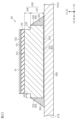
- FIG. 1 is a perspective view of a signal transmission device according to a first embodiment.
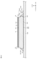
- FIG. 2 is a side view of the signal transmission device of FIG.
- FIG. 3 is a side view of the signal transmission device of FIG. 1, seen from a different direction than that of FIG.
- FIG. 4 is an enlarged view of the first lead terminal and its periphery in FIG.
- FIG. 5 is an enlarged view of an end surface of an outer lead of the first lead terminal of FIG.
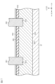
- FIG. 6 is a side view of the signal transmission device mounted on a circuit board.
- FIG. 7 is a schematic plan view showing the internal configuration of the signal transmission device of FIG.
- FIG. 8 is an enlarged view of the first frame and its surroundings in FIG.
- FIG. 9 is an enlarged view of a part of the first frame and its surroundings in FIG.
- FIG. 10 is an enlarged view of a remaining portion of the first frame in FIG. 8 and its surroundings.
- FIG. 11 is a schematic cross-sectional view of a wire connection portion of a first lead terminal.
- FIG. 12 is an enlarged view of the second die pad and its periphery in FIG.
- FIG. 13 is an enlarged view of the third die pad and its periphery in FIG.
- FIG. 14 is a schematic cross-sectional view of a wire connection portion of the second lead terminal.
- FIG. 15 is an enlarged perspective view of the second bond portion of the third die pad wire and its surroundings.
- FIG. 16 is a circuit diagram of the signal transmission device of the first embodiment.
- FIG. 17 is a schematic plan view illustrating an example of the internal structure of the first chip in the signal transmission device according to the first embodiment.
- FIG. 18 is an enlarged plan view of the transformer region of FIG.
- FIG. 19 is a schematic plan view showing an example of the internal structure of the first chip at a position different from that in FIG. 18 in the thickness direction of the first chip.
- FIG. 20 is an enlarged plan view of the transformer region of FIG.
- FIG. 21 is a cross-sectional view showing the cross-sectional structure of the first transformer of the first chip and its periphery.
- FIG. 22 is an enlarged view of a part of the first chip in FIG.
- FIG. 23 is an enlarged view of the conductor of the first surface side coil in the first chip of FIG. 22.
- FIG. FIG. 24 is an enlarged view of the conductor wire of the first back side coil in the first chip in FIG. 22.
- FIG. 25 is a cross-sectional view showing a cross-sectional structure of a part of the circuit region of the first chip.
- FIG. 26 is an enlarged view of the first via and its periphery in FIG.
- FIG. 27 is an enlarged plan view of a part of the first frame and its periphery in the signal transmission device of the second embodiment.
- FIG. 28 is an enlarged plan view of the second die pad and its periphery in the signal transmission device of the second embodiment.
- FIG. 29 is an enlarged plan view of the third die pad and its periphery in the signal transmission device of the second embodiment.
- FIG. 30 is an enlarged plan view of a part of the first frame and its periphery in the signal transmission device of the third embodiment.
- FIG. 31 is an enlarged plan view of a remaining portion of the first frame and its periphery in the signal transmission device of the third embodiment.
- FIG. 32 is an enlarged plan view of the second die pad and its periphery in the signal transmission device of the third embodiment.
- FIG. 33 is an enlarged plan view of the third die pad and its periphery in the signal transmission device of the third embodiment.
- FIG. 34 is an enlarged plan view of a part of the first frame and its periphery in the signal transmission device of the fourth embodiment.
- FIG. 35 is an enlarged plan view of a remaining portion of the first frame and its periphery in the signal transmission device of the fourth embodiment.
- FIG. 36 is an enlarged plan view of the second die pad and its periphery in the signal transmission device of the fourth embodiment.
- FIG. 37 is an enlarged plan view of the third die pad and its periphery in the signal transmission device of the fourth embodiment.
- FIG. 38 is an enlarged plan view of a part of the first die pad, the third die pad, and the periphery thereof in the signal transmission device of the fifth embodiment.
- FIG. 39 is a schematic cross-sectional view of a first chip and a first die pad in a signal transmission device according to the sixth embodiment.
- FIG. 40 is a schematic cross-sectional view of the first chip and the first die pad taken in a direction different from that of FIG.
- FIG. 41 is a schematic cross-sectional view of the second chip and the second die pad.
- FIG. 42 is a schematic cross-sectional view of the second chip and the second die pad taken in a direction different from that of FIG. FIG.
- FIG. 43 is a schematic cross-sectional view of the third chip and the third die pad.
- FIG. 44 is a schematic cross-sectional view of the third chip and the third die pad taken in a direction different from that of FIG.
- FIG. 45 is a cross-sectional view illustrating an example of a manufacturing process for the signal transmission device of the sixth embodiment.
- FIG. 46 is a cross-sectional view showing a schematic example of a manufacturing process for the signal transmission device subsequent to FIG. 45.
- FIG. 47 is a cross-sectional view showing a schematic example of a manufacturing process for the signal transmission device following FIG. 46.
- FIG. 48 is a cross-sectional view showing a schematic example of a manufacturing process for the signal transmission device following FIG. 47.
- FIG. 46 is a cross-sectional view showing a schematic example of a manufacturing process for the signal transmission device following FIG. 46.
- FIG. 49 is a plan view illustrating a schematic internal structure of the signal transmission device according to the seventh embodiment.
- FIG. 50 is a plan view illustrating a schematic internal structure of the signal transmission device according to the eighth embodiment.
- FIG. 51 is an enlarged plan view of the first frame and its periphery in the signal transmission device of the ninth embodiment.
- FIG. 52 is an enlarged plan view of the first die pad and its periphery in the signal transmission device of the ninth embodiment.
- FIG. 53 is a cross-sectional view showing a schematic example of a cross-sectional structure of a first transformer of a first chip and its periphery in a signal transmission device according to the tenth embodiment.
- FIG. 54 is an enlarged cross-sectional view of a part of the first transformer and its periphery in FIG.
- FIG. 55 is a cross-sectional view illustrating an example of a manufacturing process for the signal transmission device of the tenth embodiment.
- 56 is a cross-sectional view showing a schematic example of a manufacturing process for the signal transmission device following FIG. 55.
- FIG. 57 is a cross-sectional view showing a schematic example of a manufacturing process for the signal transmission device following FIG. 56.
- FIG. 58 is a cross-sectional view showing the cross-sectional structure of the first transformer of the first chip and part of its periphery in the signal transmission device of the eleventh embodiment.
- FIG. 60 is a cross-sectional view illustrating an example of a manufacturing process for the signal transmission device of the twelfth embodiment.
- 61 is a cross-sectional view showing a schematic example of a manufacturing process for the signal transmission device following FIG. 60.
- FIG. 62 is a cross-sectional view showing a schematic example of a manufacturing process for the signal transmission device following FIG. 61.
- FIG. 63 is a cross-sectional view showing a schematic example of a manufacturing process for the signal transmission device following FIG. 62.
- FIG. FIG. FIG. 60 is a cross-sectional view illustrating an example of a manufacturing process for the signal transmission device following FIG. 60.
- FIG. 64 is a cross-sectional view showing a schematic example of a manufacturing process for the signal transmission device following FIG. 63.
- 65 is a cross-sectional view showing a schematic example of a manufacturing process for the signal transmission device following FIG. 64.
- FIG. 66 is an enlarged cross-sectional view of a portion of the first surface side coil of the first transformer of the first chip and its surrounding area in the signal transmission device of the thirteenth embodiment.
- FIG. 67 is a cross-sectional view illustrating an example of a manufacturing process for the signal transmission device of the thirteenth embodiment.
- 68 is a cross-sectional view showing a schematic example of a manufacturing process for the signal transmission device following FIG. 67.
- FIG. 69 is a cross-sectional view showing a schematic example of a manufacturing process for the signal transmission device following FIG. 68.
- 70 is a cross-sectional view showing a schematic example of a manufacturing process for the signal transmission device subsequent to FIG. 69.
- FIG. 71 is a cross-sectional view showing a schematic example of a manufacturing process for the signal transmission device subsequent to FIG. 70.
- FIG. 72 is a schematic plan view showing an example of the internal structure of the first chip in a signal transmission device according to a modified example.
- FIG. 73 is a schematic plan view showing an example of the internal structure of the first chip at a position different from that in FIG. 72 in the thickness direction of the first chip.
- FIG. 74 is a plan view showing a schematic internal structure of a signal transmission device according to a modified example.
- FIG. 75 is a plan view showing a schematic internal structure of a signal transmission device according to a modified example.
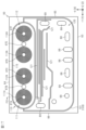
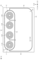
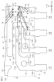
- FIG. 1 to 6 show the external structure of the signal transmission device 10.
- Figures 7 to 15 show the internal structure of the signal transmission device 10.
- Figure 16 shows the circuit configuration of the signal transmission device 10.
- Figures 17 to 26 show the internal structure of a first chip 60 (described later) of the signal transmission device 10.
- FIG. 1 shows a perspective view of the signal transmission device 10.
- Figs. 2 and 3 show a side view of the signal transmission device 10.
- Fig. 4 shows an enlarged view of a portion of a first lead terminal 18 of the signal transmission device 10, which will be described later.
- the package structure of the signal transmission device 10 is a small outline package (SOP).
- SOP small outline package
- the package structure of the signal transmission device 10 can be changed as desired, and may be a quad for non-lead package (QFN), dual flat package (DFP), dual inline package (DIP), quad flat package (QFP), single inline package (SIP), or small outline J-leaded package (SOJ), or various similar package structures.
- QFN quad for non-lead package
- DFP dual flat package
- DIP dual inline package
- QFP quad flat package
- SIP single inline package
- SOJ small outline J-leaded package
- the signal transmission device 10 includes a sealing resin 90, a plurality of first lead terminals 11-18 (eight in the first embodiment) protruding from the sealing resin 90, and a plurality of second lead terminals 41-48 (eight in the first embodiment) protruding from the sealing resin 90.
- the sealing resin 90 is formed in a rectangular plate shape.
- the thickness direction of the sealing resin 90 is the "Z direction", and two mutually perpendicular directions among the directions perpendicular to the Z direction are the "X direction” and the "Y direction”.
- the upper side of the Z direction is the "+Z direction", and the lower side is the "-Z direction”.
- the front side of the X direction is the "+X direction”
- the rear side is the "-X direction”.
- the right side of the Y direction is the "+Y direction”
- the left side is the "-Y direction”.
- planar view refers to viewing the signal transmission device 10 from the thickness direction of the sealing resin 90. Unless otherwise specified, planar view refers to viewing the signal transmission device 10 from the +Z direction.
- the shape of the sealing resin 90 in plan view is a rectangle with the X direction being the short side direction and the Y direction being the long side direction.
- the size of the sealing resin 90 in the Y direction is at least twice the size of the sealing resin 90 in the X direction.
- the size of the sealing resin 90 in the Y direction is no more than three times the size of the sealing resin 90 in the X direction. In one example, in plan view, the size of the sealing resin 90 in the Y direction is about 2.5 times the size of the sealing resin 90 in the X direction.
- the dimension of the sealing resin 90 in the X direction is about 4.0 mm
- the dimension of the sealing resin 90 in the Y direction is about 10.0 mm
- the dimension (thickness) of the sealing resin 90 in the Z direction is about 1.75 mm.
- the sealing resin 90 has a sealing surface 91, a sealing back surface 92 opposite the sealing surface 91, and first to fourth sealing side surfaces 93 to 96 connecting the sealing surface 91 and the sealing back surface 92.
- the sealing surface 91 is a surface facing the +Z direction
- the sealing back surface 92 is a surface facing the -Z direction.
- the first sealing side surface 93 and the second sealing side surface 94 form both end surfaces of the sealing resin 90 in the X direction
- the third sealing side surface 95 and the fourth sealing side surface 96 form both end surfaces of the sealing resin 90 in the Y direction.
- the first sealing side surface 93 is a surface facing the +X direction
- the second sealing side surface 94 is a surface facing the -X direction.
- the third sealing side surface 95 is a surface facing the +Y direction
- the fourth sealing side surface 96 is a surface facing the -Y direction.
- a recess 91A is formed in the sealing surface 91.
- the recess 91A is circular in a plan view.
- the recess 91A is recessed in a curved concave shape from the sealing surface 91.
- the recess 91A is formed in a portion of the sealing surface 91 that is closer to the first sealing side surface 93 and the fourth sealing side surface 96.
- the recess 91A serves as a marker for distinguishing the first lead terminals 11-18 from the second lead terminals 41-48.
- the first sealing side 93 includes a first front side 93A that is continuous with the sealing surface 91, a first back side 93B that is continuous with the sealing back surface 92, and a first central side 93C.
- the second sealing side 94 includes a second front side 94A that is continuous with the sealing surface 91, a second back side 94B that is continuous with the sealing back surface 92, and a second central side 94C.
- the first front side 93A and the second front side 94A are inclined in a direction away from each other as they move from the sealing surface 91 toward the sealing back surface 92.
- the connection portion between the first front side 93A and the sealing surface 91 is formed with an inclined surface 93AA.
- the angle formed by the inclined surface 93AA and the Z direction is larger than the angle formed by the first front side 93A and the Z direction.
- the angle formed by the inclined surface 93AA and the Z direction is, for example, 45°.
- the connection portion between the second front surface side surface 94A and the sealing surface 91 is formed in a curved shape.
- the first back surface side surface 93B and the second back surface side surface 94B are inclined in a direction away from each other as they move from the sealing back surface 92 to the sealing surface 91.
- the connection portion between the first back surface side surface 93B and the second back surface side surface 94B and the sealing back surface 92 is formed in a curved shape.
- the first central side surface 93C is formed between the first front surface side surface 93A and the first back surface side surface 93B in the Z direction.
- the first central side surface 93C is connected to both the first front surface side surface 93A and the first back surface side surface 93B.
- the first central side surface 93C is formed as a flat surface along, for example, the YZ plane.
- the second central side surface 94C is formed between the second front surface side surface 94A and the second back surface side surface 94B in the Z direction.
- the second central side surface 94C is connected to both the second front surface side surface 94A and the second back surface side surface 94B.
- the second central side surface 94C is formed as a flat surface along the YZ plane, for example.
- the third sealing side 95 includes a third front side 95A that is continuous with the sealing surface 91, a third back side 95B that is continuous with the sealing back surface 92, and a third central side 95C.
- the fourth sealing side 96 includes a fourth front side 96A that is continuous with the sealing surface 91, a fourth back side 96B that is continuous with the sealing back surface 92, and a fourth central side 96C.
- the third front side 95A and the fourth front side 96A are inclined in directions away from each other as they move from the sealing surface 91 to the sealing back surface 92.
- the connection portions between the third front side 95A and the fourth front side 96A and the sealing surface 91 are formed in a curved shape.
- the third back side 95B and the fourth back side 96B are inclined in directions away from each other as they move from the sealing back surface 92 to the sealing surface 91.
- the connection portions between the third back side 95B and the fourth back side 96B and the sealing back surface 92 are formed in a curved shape.
- the third central side surface 95C is connected to both the third front surface side surface 95A and the third back surface side surface 95B.
- the third central side surface 95C is formed, for example, as a flat surface along the XZ plane.
- the fourth central side surface 96C is formed between the fourth front surface side surface 96A and the fourth back surface side surface 96B in the Z direction.
- the fourth central side surface 96C is connected to both the fourth front surface side surface 96A and the fourth back surface side surface 96B.
- the fourth central side surface 96C is formed, for example, as a flat surface along the XZ plane.
- the sealing resin 90 is formed, for example, by transfer molding.
- the third sealing side surface 95 is provided with a trace (not shown) of the gate of the molding die. This trace is formed when the resin portion located at the gate of the molding die is separated from the sealing resin 90.
- the trace is formed, for example, on the third central side surface 95C of the third sealing side surface 95.
- the third central side surface 95C is partitioned into three regions R1 to R3 in the X direction.
- the regions R1 to R3 are regions of the same size.
- the region R1 is a region of the third central side surface 95C closer to the first sealing side surface 93
- the region R3 is a region of the third central side surface 95C closer to the second sealing side surface 94
- the region R2 is a region between the regions R1 and R3 in the X direction.
- the above-mentioned trace may be provided in the region R1.
- the above-mentioned trace may also be provided in the region R2.
- the above-mentioned trace may also be provided in the region R3.
- the gate trace of the molding die may be formed on the fourth sealing side surface 96 instead of the third sealing side surface 95. Even in this case, the trace is formed, for example, on the fourth central side surface 96C of the fourth sealing side surface 96.
- the surface roughness Rz of each of the sealing surface 91, sealing back surface 92, and first to fourth sealing side surfaces 93 to 96 of the sealing resin 90 is, for example, 5 ⁇ m or more and 20 ⁇ m or less.
- the surface roughness Rz over the entire surface of each of the sealing surface 91 and sealing back surface 92 is, for example, 5 ⁇ m or more and 20 ⁇ m or less.
- the surface roughness Rz over the entire surface of each of the first to fourth front side surfaces 93A to 96A and the first to fourth back side surfaces 93B to 96B of the first to fourth sealing side surfaces 93 to 96 is, for example, 5 ⁇ m or more and 20 ⁇ m or less.
- the surface roughness Rz can be expressed as the sum of the height of the highest peak and the depth of the deepest valley among the contour curves at the reference length.
- the sealing surface 91, sealing back surface 92, and first to fourth sealing side surfaces 93 to 96 are roughened to have each surface roughness Rz of, for example, 5 ⁇ m or more and 20 ⁇ m or less.
- An example of surface roughening is shot blasting.
- the surface roughness Rz of each of the sealing surface 91, the sealing back surface 92, and the first to fourth sealing side surfaces 93 to 96 is, for example, 8 ⁇ m or more. In one example, the surface roughness Rz of each of the sealing surface 91, the sealing back surface 92, and the first to fourth sealing side surfaces 93 to 96 is, for example, 8 ⁇ m or more and 20 ⁇ m or less.
- the surface roughness Rz of the sealing surface 91 and the sealing back surface 92, and the first to fourth front side surfaces 93A to 96A and the first to fourth back side surfaces 93B to 96B may be greater than that of the first to fourth central side surfaces 93C to 95C. In one example, the surface roughness Rz of the sealing surface 91 and the sealing back surface 92, and the first to fourth front side surfaces 93A to 96A and the first to fourth back side surfaces 93B to 96B may be greater than the surface roughness Rz of the surfaces that make up the recess 91A.
- the surface roughness Rz of the sealing surface 91, the sealing back surface 92, and the first to fourth sealing side surfaces 93 to 96 was 5 ⁇ m or more and 20 ⁇ m or less, but this is not limited to this.
- the surface roughness Rz of each of the third sealing side surface 95 and the fourth sealing side surface 96 may be less than 5 ⁇ m or greater than 20 ⁇ m.
- the surface roughness Rz of each of the first sealing side surface 93 and the second sealing side surface 94 may be less than 5 ⁇ m or greater than 20 ⁇ m.
- the surface roughness Rz of each of the first to fourth sealing side surfaces 93 to 96 may be less than 5 ⁇ m or greater than 20 ⁇ m.
- the surface roughness Rz of the sealing surface 91 may be less than 5 ⁇ m or greater than 20 ⁇ m. In short, it is sufficient that the surface roughness Rz of at least one of the sealing surface 91, the sealing back surface 92, and the first to fourth sealing side surfaces 93 to 96 is 5 ⁇ m or more and 20 ⁇ m or less.
- the sealing resin 90 is made of an insulating material.
- One example of the insulating material is black epoxy resin.
- the sealing resin 90 contains sulfur (S) as an additive. By containing sulfur, the sealing resin 90 can increase the adhesive strength with the first frame 10A and the second frame 10B described below. On the other hand, by containing sulfur, the sealing resin 90 may cause sulfide corrosion of the copper-based components in the signal transmission device 10.
- the concentration of sulfur added to the sealing resin 90 is set in consideration of the balance between improving the adhesive strength between the first frame 10A and the second frame 10B and the sealing resin 90 and suppressing sulfide corrosion. In one example, the concentration of sulfur added to the sealing resin 90 is set to 300 ⁇ g/g or less.
- the first lead terminals 11-18 include first outer lead portions 11B-18B protruding outward from the sealing resin 90.
- the first outer lead portions 11B-18B protrude from the first sealing side surface 93 toward the +X direction.
- the first outer lead portions 11B-18B are arranged at a distance from each other in the Y direction. It can be said that the first outer lead portions 11B-18B are arranged in the longitudinal direction of the sealing resin 90.
- the first outer lead portions 11B-18B are arranged in the order of the first outer lead portions 11B, 12B, 13B, 14B, 15B, 16B, 17B, and 18B from the fourth sealing side surface 96 toward the third sealing side surface 95.
- the Y direction can be said to be the arrangement direction of the first outer lead portions 11B-18B.
- the Y direction can be said to be the arrangement direction of the first lead terminals 11-18.
- the first outer lead portions 11B to 18B have the same shape.
- the second lead terminals 41 to 48 include second outer lead portions 41B to 48B that protrude from the sealing resin 90 to the outside.
- the second outer lead portions 41B to 48B protrude from the second sealing side surface 94 toward the -X direction.
- the second outer lead portions 41B to 48B are arranged at a distance from each other in the Y direction. It can be said that the second outer lead portions 41B to 48B are arranged in the longitudinal direction of the sealing resin 90.
- the second outer lead portions 41B to 48B are arranged in the order of the second outer lead portions 41B, 42B, 43B, 44B, 45B, 46B, 47B, and 48B from the third sealing side surface 95 toward the fourth sealing side surface 96.
- the Y direction can be said to be the arrangement direction of the second outer lead portions 41B to 48B.
- the Y direction can be said to be the arrangement direction of the second lead terminals 41 to 48.
- the second outer lead portions 41B to 48B have the same shape.
- the width dimension (size in the Y direction) of the first outer lead portions 11B to 18B and the width dimension (size in the Y direction) of the second outer lead portions 41B to 48B are equal to each other.
- the width dimension of the first outer lead portions 11B to 18B and the width dimension of the second outer lead portions 41B to 48B are, for example, about 0.41 mm.
- the pitch of the first outer lead portions 11B to 18B and the pitch of the second outer lead portions 41B to 48B are equal to each other.
- the pitch of the first outer lead portions 11B to 18B can be defined by the center-to-center distance between two outer lead portions adjacent in the Y direction among the first outer lead portions 11B to 18B.
- the pitch of the second outer lead portions 41B to 48B can be defined by the center-to-center distance between two outer lead portions adjacent in the Y direction among the second outer lead portions 41B to 48B.
- the pitch of the first outer lead portions 11B to 18B and the pitch of the second outer lead portions 41B to 48B are each, for example, approximately 1.27 mm.
- the shape of the first outer lead portion 18B and the shape of the second outer lead portion 41B when viewed from the Y direction are the same. Therefore, it can be said that the shapes of the first outer lead portions 11B to 18B and the shapes of the second outer lead portions 41B to 48B are the same.
- first outer lead portions 11B to 18B The configuration of the first outer lead portions 11B to 18B will be described. Below, the detailed configuration of the first outer lead portion 18B will be described, and the detailed configuration of the first outer lead portions 11B to 17B will be omitted.
- the first outer lead portion 18B includes a protruding portion 18P extending in the +X direction from the first sealing side surface 93, an intermediate portion 18Q extending in the -Z direction from the protruding portion 18P, and a connecting portion 18R extending in the +X direction from the intermediate portion 18Q.
- a curved first bend is formed between the protruding portion 18P and the intermediate portion 18Q
- a curved second bend is formed between the intermediate portion 18Q and the connecting portion 18R.
- the connecting portion 18R may be inclined toward the -Z direction as it approaches the +X direction.
- the acute angle formed by the connecting portion 18R and the X direction is, for example, greater than 0° and equal to or less than 8°.
- the first outer lead portion 18B includes an outer lead body 20A made of a metal material.
- metal materials include copper and aluminum.
- the outer lead body 20A has an outer lead surface 21A, an outer lead back surface 22A opposite the outer lead surface 21A, a pair of outer lead side surfaces 23A (see FIG. 5) connecting the outer lead surface 21A and the outer lead back surface 22A, and an outer lead end surface 24A.
- the outer lead end surface 24A forms the tip surface of the connection portion 18R.
- the pair of outer lead side surfaces 23A are formed in a curved concave shape.
- the deepest position of the curved concave outer lead side surface 23A (the position where the pair of outer lead side surfaces 23A are closest to each other in the Y direction) is closer to the outer lead back surface 22A than the center in the Z direction of the outer lead end surface 24A.
- the outer lead body 20A has a backside curved portion 25 formed at the connection between the outer lead backside 22A and the outer lead side surface 23A.
- the backside curved portion 25 curves upward (+Z direction) as it moves outward in the width direction (Y direction) of the outer lead body 20A. Therefore, both ends of the outer lead backside 22A in the Y direction are curved upward (+Z direction) as they move toward the pair of outer lead side surfaces 23A.
- the first outer lead portion 18B includes a plating layer 26 that covers the outer lead body 20A. More specifically, the plating layer 26 covers the entire surfaces of the outer lead surface 21A, the outer lead back surface 22A, and the outer lead side surface 23A, as well as a portion of the outer lead end surface 24A.
- the plating layer 26 includes an end surface plating layer 27 that covers the outer lead end surface 24A continuously from the outer lead back surface 22A toward the outer lead surface 21A.
- the end surface plating layer 27 is located away in the Z direction from the edge of the outer lead end surface 24A on the outer lead surface 21A side. Therefore, the outer lead end surface 24A is divided into an area covered by the end surface plating layer 27 and a main body exposed area 28 that is not covered by the end surface plating layer 27. In the main body exposed area 28, the outer lead main body 20A is exposed.
- the end surface plating layer 27 extends from the outer lead back surface 22A to a position closer to the outer lead surface 21A than the center of the outer lead end surface 24A in the Z direction. In one example, the end surface plating layer 27 covers approximately 2/3 of the outer lead end surface 24A in the Z direction.
- the tip edge 27A of the end surface plating layer 27 includes a shape that becomes uneven in the Z direction as it approaches the Y direction. In one example, the tip edge 27A of the end surface plating layer 27 includes a recess 27B near the center in the Y direction.
- leading edge 27A of the end surface plating layer 27 can be changed as desired.
- the leading edge 27A of the end surface plating layer 27 may include a plurality of recesses 27B.
- the recesses 27B may be omitted from the leading edge 27A of the end surface plating layer 27.
- the position of the tip edge 27A of the end surface plating layer 27 in the Z direction can be changed arbitrarily.
- the end surface plating layer 27 may cover about 1/2 of the outer lead end surface 24A in the Z direction.
- the end surface plating layer 27 may cover about 1/4 of the outer lead end surface 24A in the Z direction.
- the end surface plating layer 27 may cover about 3/4 of the outer lead end surface 24A in the Z direction. In this way, the end surface plating layer 27 may cover a range of 1/4 to 3/4 of the outer lead end surface 24A in the Z direction.
- the configuration of the second outer lead portions 41B to 48B will be described. Below, the detailed configuration of the second outer lead portion 41B will be described, and the detailed configuration of the second outer lead portions 42B to 48B will be omitted.
- the second outer lead portion 41B includes a protruding portion 41P extending in the -X direction from the second sealing side surface 94, an intermediate portion 41Q extending in the -Z direction from the protruding portion 41P, and a connecting portion 41R extending in the -X direction from the intermediate portion 41Q.
- a curved first bend is formed between the protruding portion 41P and the intermediate portion 41Q
- a curved second bend is formed between the intermediate portion 41Q and the connecting portion 41R.
- the connecting portion 41R may be inclined toward the -Z direction as it approaches the -X direction.
- the acute angle formed by the connecting portion 41R and the X direction is, for example, greater than 0° and equal to or less than 8°.
- the second outer lead portion 41B like the first outer lead portion 18B, includes an outer lead body 20A and a plating layer 26 (see FIG. 4) that covers the outer lead body 20A.
- the plating layer 26 of the second outer lead portion 41B like the first outer lead portion 18B, also includes an end face plating layer 27 (see FIG. 4).
- a method for forming such an end surface plating layer 27 will be described below.
- a first lead frame (not shown) constituting the first outer lead portion 18B and a second lead frame (not shown) constituting the second outer lead portion 41B are cut by a die (punch).
- the cutting by the die can be performed, for example, on the first lead frame and the second lead frame connected to the frame.
- the outer leads 11B to 18B, 41B to 48B formed by cutting are formed.
- both the first lead frame and the second lead frame before being cut by the mold include an outer lead body 20A and a plating layer 26 that covers the outer lead surface 21A, the outer lead back surface 22A, and the pair of outer lead side surfaces 23A.
- the mold cuts the first lead frame and the second lead frame in the +Z direction for both the first lead frame and the second lead frame. This forms the first outer lead portion 18B and the second outer lead portion 41B, each of which includes the outer lead end surface 24A.
- the corners of the cut portion in the mold are rounded and curved. In other words, the corners are chamfered.
- the plating layer 26 on the back surface 22A of the outer lead is pulled toward the outer lead surface 21A, forming an end surface plating layer 27 on the outer lead end surface 24A.
- the end surface plating layer 27 is formed on both the first outer lead portion 18B and the second outer lead portion 41B, so that when the signal transmission device 10 is mounted on the circuit board PCB by a conductive bonding material SD such as solder paste or silver (Ag) paste, as shown in FIG. 6, the bonding area between the first outer lead portion 18B and the second outer lead portion 41B and the conductive bonding material SD can be increased. More specifically, the outer lead back surface 22A of the connection portion 18R of the first outer lead portion 18B, the pair of outer lead side surfaces 23A (see FIG. 5), and the outer lead back surface 22A of the end of the intermediate portion 18Q on the connection portion 18R side are each bonded to the conductive bonding material SD.
- a conductive bonding material SD such as solder paste or silver (Ag) paste
- the end surface plating layer 27 of the first outer lead portion 18B bonds the outer lead end surface 24A (see FIG. 5) of the first outer lead portion 18B to the conductive bonding material SD.
- the bonding area between the first outer lead portion 18B and the conductive bonding material SD is increased by the bonding area between the end surface plating layer 27 and the conductive bonding material SD.
- the outer lead back surface 22A of the connection portion 41R of the second outer lead portion 41B, the pair of outer lead side surfaces 23A, and the outer lead back surface 22A of the end of the intermediate portion 41Q on the connection portion 41R side are each bonded to the conductive bonding material SD.
- the end surface plating layer 27 of the second outer lead portion 41B bonds the outer lead end surface 24A of the second outer lead portion 41B to the conductive bonding material SD.
- the bonding area between the second outer lead portion 41B and the conductive bonding material SD is increased by the bonding area between the end surface plating layer 27 and the conductive bonding material SD.
- a fillet is formed by the conductive bonding material SD bonded to each end surface plating layer 27 of the first outer lead portion 18B and the second outer lead portion 41B.
- the bonding area with the conductive bonding material SD is also increased and fillets are formed for the first outer lead portions 11B-17B and the second outer lead portions 42B-48B (both see FIG. 1).
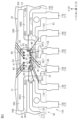
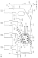
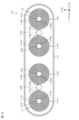
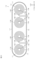
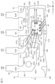
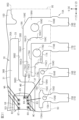
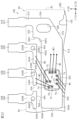
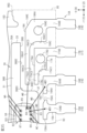
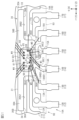
- FIG. 7 shows the overall internal structure of the signal transmission device 10.
- the sealing resin 90 is indicated by a two-dot chain line.
- the signal transmission device 10 includes a first frame 10A, a second frame 10B, a first chip 60 mounted on the first frame 10A, and a second chip 70 and a third chip 80 mounted on the second frame 10B.
- the sealing resin 90 seals the first chip 60, the second chip 70, and the third chip 80, and also partially seals the first frame 10A and the second frame 10B.
- the first frame 10A includes first lead terminals 11-18.
- the first frame 10A further includes a first die pad 30.
- the first lead terminals 11-18 and the first die pad 30 are formed from the same metal material. Examples of metal materials include copper and aluminum.
- the first lead terminal 14 that is located near the center in the Y direction is connected to the first die pad 30.
- the first lead terminal 14 and the first die pad 30 are integrated.
- the first lead terminals 11 to 13 and 15 to 18 are arranged at a distance from the first die pad 30. As shown in FIG. 7, the first lead terminals 11 to 18 can be said to be arranged at a distance from each other in the Y direction.
- the first die pad 30 is disposed closer to the first sealing side surface 93 than the center of the sealing resin 90 in the X direction.
- the first chip 60 mounted on the first die pad 30 is formed in a flat plate shape.
- the shape of the first chip 60 in a plan view is rectangular with the X direction as the short side direction and the Y direction as the long side direction.
- the first chip 60 is mounted on the first die pad 30 by a first conductive bonding material SD1. More specifically, the first chip 60 is die-bonded to the first die pad 30.
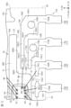
- the second frame 10B is disposed apart from the first frame 10A in the X direction. That is, in the first embodiment, the X direction is the arrangement direction of the first frame 10A and the second frame 10B.
- the second frame 10B includes second lead terminals 41-48.
- the second frame 10B further includes a second die pad 50A and a third die pad 50B.
- the second lead terminals 41-48, the second die pad 50A, and the third die pad 50B are formed of the same metal material. Examples of the metal material include copper and aluminum.
- the second lead terminals 41-48, the second die pad 50A, and the third die pad 50B are formed of the same metal material as the first lead terminals 11-18 and the first die pad 30.
- the second lead terminal 41 which is located at the end closer to the third sealing side surface 95, of the second lead terminals 41 to 48, is connected to the second die pad 50A.
- the second lead terminal 41 and the second die pad 50A are integrated.
- the second lead terminal 46 which is located closer to the fourth sealing side surface 96, of the second lead terminals 41 to 48, is connected to the third die pad 50B.
- the second lead terminal 46 and the third die pad 50B are integrated.
- the second lead terminals 42 to 45 which are arranged between the second lead terminal 41 and the second lead terminal 46 in the Y direction, are arranged at a distance from the second die pad 50A and the third die pad 50B.
- the second lead terminals 47 and 48 which are closer to the fourth sealing side surface 96 than the second lead terminal 46, are arranged at a distance from the third die pad 50B. As shown in FIG. 7, the second lead terminals 41 to 48 can be said to be arranged at a distance from each other in the Y direction.
- Both the second die pad 50A and the third die pad 50B are arranged in the X direction away from the first die pad 30 and closer to the second sealing side surface 94.
- the X direction can be said to be the arrangement direction of the first die pad 30, the second die pad 50A, and the third die pad 50B. It can also be said that the first die pad 30, the second die pad 50A, and the third die pad 50B are arranged in the short direction of the sealing resin 90. Both the second die pad 50A and the third die pad 50B are arranged closer to the second sealing side surface 94 than the center of the sealing resin 90 in the X direction. Both the second die pad 50A and the third die pad 50B are arranged opposite the first die pad 30 in the X direction.
- the first die pad 30 has a size in the Y direction that allows it to face the second die pad 50A and the third die pad 50B.
- the X direction corresponds to the "first direction”.
- the second die pad 50A and the third die pad 50B are arranged on the opposite side of the first die pad 30 in the X direction from the side on which the first lead terminals 11 to 18 are arranged.
- the first lead terminals 11 to 18 are arranged on the opposite side of the first die pad 30 in the X direction from the second die pad 50A and the third die pad 50B.
- the second lead terminals 41 to 48 are arranged on the opposite side of the second die pad 50A and the third die pad 50B from the first die pad 30 in the X direction.
- the second die pad 50A and the third die pad 50B are spaced apart from each other in the Y direction. That is, in the first embodiment, the Y direction is the arrangement direction of the second die pad 50A and the third die pad 50B.
- the second die pad 50A is arranged closer to the third sealing side surface 95 than the third die pad 50B.
- the second die pad 50A is arranged closer to the third sealing side surface 95 than the center of the sealing resin 90 in the Y direction.
- the third die pad 50B is arranged closer to the fourth sealing side surface 96 than the center of the sealing resin 90 in the Y direction.
- the Y direction corresponds to the "second direction".
- the second chip 70 mounted on the second die pad 50A is formed in a flat plate shape.
- the shape of the second chip 70 in a plan view is rectangular with the X direction being the short side direction and the Y direction being the long side direction.
- the size of the second chip 70 in the X direction is smaller than the size of the first chip 60 in the X direction.
- the size of the second chip 70 in the Y direction is smaller than the size of the first chip 60 in the Y direction.
- the second chip 70 is mounted on the second die pad 50A by the second conductive bonding material SD2. More specifically, the second chip 70 is die-bonded to the second die pad 50A.
- the third chip 80 mounted on the third die pad 50B is formed in a flat plate shape.
- the shape of the third chip 80 in a plan view is a rectangle with the X direction being the short side direction and the Y direction being the long side direction.
- the size of the third chip 80 in the X direction is smaller than the size of the first chip 60 in the X direction.
- the size of the third chip 80 in the Y direction is smaller than the size of the first chip 60 in the Y direction.
- the sizes of the third chip 80 in the X direction and the Y direction are the same as the sizes of the second chip 70 in the X direction and the Y direction.
- the third chip 80 is mounted on the third die pad 50B by the third conductive bonding material SD3. More specifically, the third chip 80 is die-bonded to the third die pad 50B. Note that, for example, solder paste or silver paste is used as the first to third conductive bonding materials SD1 to SD3.
- the second chip 70 is disposed closer to the third die pad 50B of the second die pad 50A. When viewed from the X direction, the second chip 70 is disposed closer to the third sealing side surface 95 than the first chip 60. The third chip 80 is disposed closer to the fourth sealing side surface 96 than the first chip 60.
- the signal transmission device 10 further includes conductive members 10D and 10E.
- the conductive members 10D and 10E are formed, for example, from the same metal material as the first frame 10A and the second frame 10B.
- the conductive members 10D and 10E are disposed at a distance from each other. Furthermore, the conductive members 10D and 10E are disposed at a distance from both the first frame 10A and the second frame 10B. Therefore, both conductive members 10D and 10E are in an electrically floating state.
- the conductive members 10D and 10E are disposed in positions overlapping each other when viewed from the Y direction.
- the conductive members 10D and 10E are disposed in the center of the sealing resin 90 in the Y direction.
- the conductive member 10D is disposed closer to the third sealing side surface 95 than the first frame 10A and the second frame 10B.
- the conductive member 10D is exposed from the third sealing side surface 95. More specifically, a recess 95D is formed in a portion of the third sealing side surface 95 where the conductive member 10D is exposed.
- the recess 95D is formed in the center of the third sealing side surface 95 in the Z direction. That is, the recess 95D is provided in the third central side surface 95C (see FIG. 2).
- the recess 95D is recessed from the third sealing side surface 95 toward the fourth sealing side surface 96.
- the recess 95D is open toward the +Y direction.
- the conductive member 10D constitutes the bottom surface of the recess 95D.
- the conductive member 10E is disposed closer to the fourth sealing side surface 96 than the first frame 10A and the second frame 10B.
- the conductive member 10E is exposed from the fourth sealing side surface 96. More specifically, a recess 96D is formed in the portion of the fourth sealing side surface 96 where the conductive member 10E is exposed.
- the recess 96D is formed in the center of the fourth sealing side surface 96 in the Z direction. In other words, the recess 96D is provided in the fourth central side surface 96C (see FIG. 2).
- the recess 96D is recessed from the fourth sealing side surface 96 toward the third sealing side surface 95.
- the recess 96D is open toward the -Y direction.
- the conductive member 10E forms the bottom surface of the recess 96D.
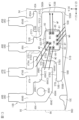
- the first die pad 30 is formed in a substantially T-shape in plan view.
- the first die pad 30 has a first tip surface 31, a first base end surface 32, a first side surface 33, and a second side surface 34.
- the first tip surface 31 is the end surface closest to the second sealing side surface 94 (see Fig. 7) among both end surfaces of the first die pad 30 in the X direction
- the first base end surface 32 is the end surface closest to the first sealing side surface 93 among both end surfaces of the first die pad 30 in the X direction.
- the first side surface 33 is the end surface closest to the third sealing side surface 95 (see Fig.
- the first tip surface 31 is a surface that faces both the second die pad 50A and the third die pad 50B (see FIG. 7 ) in the X direction and extends along the Y direction in a plan view.
- the length of the first tip surface 31 in the Y direction is longer than the length of the first base end surface 32 in the Y direction.
- Both the first side surface 33 and the second side surface 34 are surfaces that extend along the X direction in a plan view.
- the first die pad 30 further has a first tip side curved surface 35A and a second tip side curved surface 35B.
- the first tip side curved surface 35A is formed between the first tip surface 31 and the first side surface 33.
- the first tip side curved surface 35A has a shape in which the portion between the first tip surface 31 and the first side surface 33 is R-chamfered.
- the second tip side curved surface 35B is formed between the first tip surface 31 and the second side surface 34.
- the second tip side curved surface 35B has a shape in which the portion between the first tip surface 31 and the second side surface 34 is R-chamfered.
- the arc length of the first tip side curved surface 35A and the arc length of the second tip side curved surface 35B are equal to each other. In one example, it can be said that the curvature radius of the first tip side curved surface 35A and the curvature radius of the second tip side curved surface 35B are equal to each other in a plan view.
- the first die pad 30 further has a first recess 36A into which the first lead terminals 11 to 13 fit, a second recess 36B into which the first lead terminals 17 and 18 fit, and a third recess 36C into which the first lead terminals 15 and 16 fit.
- the first recessed portion 36A is formed in a portion of the first die pad 30 closer to the fourth sealing side surface 96.
- the first recessed portion 36A is formed to be recessed in the X direction from the second side surface 34 toward the first side surface 33.
- the first recessed portion 36A is formed closer to the first sealing side surface 93 than the first tip surface 31 in the X direction.
- the first recessed portion 36A is formed to remove the first base end surface 32.
- the first recessed portion 36A opens toward both the first sealing side surface 93 and the fourth sealing side surface 96.
- a first tip side protrusion 38A is provided as a portion of the first die pad 30 between the first recessed portion 36A and the first tip surface 31 in the X direction.
- the first tip side protrusion 38A extends in the Y direction.
- the first tip side protrusion 38A includes the second side surface 34, the first tip surface 31, and the second tip side curved surface 35B.
- the first tip protrusion 38A faces the third die pad 50B (see FIG. 7) in the X direction.
- the first recessed portion 36A includes a first surface 36A1 extending in the X direction, a second surface 36A2 extending in the Y direction, and a curved recess 36A3 formed between the first surface 36A1 and the second surface 36A2.
- the first surface 36A1 is disposed closer to the first side surface 33 than the second side surface 34, and is connected to the first base end surface 32.
- the second surface 36A2 constitutes a part of the side surface of the first tip side protrusion 38A.
- the curved recess 36A3 is formed as an arc portion connecting the first surface 36A1 and the second surface 36A2.
- the arc length of the curved recess 36A3 is greater than the arc length of the second tip side curved surface 35B.
- the radius of curvature of the curved recess 36A3 is greater than the radius of curvature of the second tip side curved surface 35B.
- the second recessed portion 36B is formed in a portion of the first die pad 30 closer to the third sealing side surface 95.
- the second recessed portion 36B is formed to be recessed in the X direction from the first side surface 33 toward the second side surface 34.
- the second recessed portion 36B is formed closer to the first sealing side surface 93 than the first tip surface 31 in the X direction.
- the second recessed portion 36B is formed to remove the first base end surface 32.
- the second recessed portion 36B opens toward both the first sealing side surface 93 and the third sealing side surface 95.
- a second tip side protrusion 38B is provided as a portion of the first die pad 30 between the second recessed portion 36B and the first tip surface 31 in the X direction.
- the second tip side protrusion 38B extends in the Y direction.
- the second tip side protrusion 38B includes the first side surface 33, the first tip surface 31, and the first tip side curved surface 35A.
- the second tip protrusion 38B faces the second die pad 50A (see FIG. 7) in the X direction.
- the second recessed portion 36B includes a first surface 36B1 extending in the X direction, a second surface 36B2 extending in the Y direction, and a curved recess 36B3 formed between the first surface 36B1 and the second surface 36B2.
- the first surface 36B1 is disposed closer to the second side surface 34 than the first side surface 33.
- the length of the first surface 36B1 is shorter than the length of the first surface 36A1 of the first recessed portion 36A.
- the second surface 36B2 constitutes a part of the side surface of the second tip side protrusion 38B.
- the length of the second surface 36B2 is shorter than the length of the second surface 36A2 of the first recessed portion 36A.
- the curved recess 36B3 is formed as an arc portion connecting the first surface 36B1 and the second surface 36B2.
- the arc length of the curved recess 36B3 is greater than the arc length of the first tip side curved surface 35A.
- the radius of curvature of the curved recess 36B3 is greater than the radius of curvature of the first distal curved surface 35A.
- the arc length of the curved recess 36B3 is equal to the arc length of the curved recess 36A3 of the first recess 36A.
- the radius of curvature of the curved recess 36B3 is equal to the radius of curvature of the curved recess 36A3.
- the third recessed portion 36C is formed between the first recessed portion 36A and the second recessed portion 36B in the Y direction.
- the third recessed portion 36C is formed apart from the first recessed portion 36A, but is formed continuously with the second recessed portion 36B.
- the third recessed portion 36C is formed apart from the first tip surface 31 in the X direction.
- the third recessed portion 36C is formed so as to remove the first base end surface 32.
- the third recessed portion 36C opens in both directions of the first sealing side surface 93 and the third sealing side surface 95.
- the first recessed portion 36A and the third recessed portion 36C form a connection portion 39 to which the first lead terminal 14 of the first die pad 30 is connected.
- the connection portion 39 includes the first base end surface 32.
- the third recess 36C includes a first surface 36C1 extending in the X direction, a second surface 36C2 extending in the Y direction, and a curved recess 36C3 formed between the first surface 36C1 and the second surface 36C2.
- the first surface 36C1 constitutes the side surface of the connection portion 39.
- the first surface 36C1 is formed in a position between the first surface 36A1 of the first recess 36A and the first surface 36B1 of the second recess 36B, closer to the first surface 36A1, in the Y direction.
- the first surface 36C1 is connected to the first base end surface 32.
- the length of the first surface 36C1 is shorter than the length of the first surface 36B1 of the second recess 36B.
- the second surface 36C2 is formed in a position between the second surface 36B2 of the second recess 36B and the first base end surface 32, closer to the first base end surface 32, in the X direction.
- the length of the second surface 36C2 is shorter than the length of the second surface 36B2 of the second recessed portion 36B.
- the curved recessed portion 36C3 is formed as an arc portion connecting the first surface 36C1 and the second surface 36C2.
- the arc length of the curved recessed portion 36C3 is equal to the arc length of the first tip side curved surface 35A.
- the radius of curvature of the curved recessed portion 36C3 is equal to the radius of curvature of the first tip side curved surface 35A.
- the arc length of the curved recessed portion 36C3 is smaller than the arc length of the curved recessed portions 36A3 and 36B3 of the first recessed portion 36A and the second recessed portion 36B.
- the radius of curvature of the curved recessed portion 36C3 is smaller than the radius of curvature of the curved recessed portions 36A3 and 36B3.
- an inclined surface 37 is formed between the second recess 36B and the third recess 36C.
- the inclined surface 37 extends obliquely from the first surface 36C1 to the first surface 36B1 as it moves from the second surface 36C2 to the second surface 36B2.
- the inclined surface 37 connects the second surface 36C2 and the first surface 36B1.
- each of the first lead terminals 11 to 18 will now be described. 7, of the first lead terminals 11 to 18, the first lead terminals 11 to 13 are disposed closer to the fourth sealing side surface 96 than the first chip 60 when viewed from the X direction.
- the first lead terminals 16 to 18 are disposed closer to the third sealing side surface 95 than the first chip 60 when viewed from the X direction.
- the first lead terminals 14 and 15 are disposed at positions overlapping with the first chip 60 when viewed from the X direction.
- the first lead terminals 11-18 include first inner lead portions 11A-18A provided within the sealing resin 90 and the first outer lead portions 11B-18B described above.
- the configuration of the first inner lead portions 11A-18A will be described below.
- each of the first inner lead portions 11 A to 13 A of the first lead terminals 11 to 13 includes a portion that fits into the first recessed portion 36 A of the first die pad 30 .
- the first lead terminal 11 is formed in an L-shape in a plan view and includes a wire connection portion 11AA and a lead connection portion 11AB extending from the wire connection portion 11AA toward the first sealing side surface 93.
- the wire connection portion 11AA fits into the first recessed portion 36A of the first die pad 30.
- the wire connection portion 11AA extends in the Y direction.
- the wire connection portion 11AA includes a recessed portion 11AC.
- the recessed portion 11AC is formed in a portion of the wire connection portion 11AA closer to the first lead terminal 12.
- the recessed portion 11AC is recessed from the end of the wire connection portion 11AA closer to the first sealing side surface 93 in the X direction toward the second tip side protrusion 38B of the first die pad 30.
- the recessed portion 11AC includes a first surface 11AC1 extending in the X direction, a second surface 11AC2 extending in the Y direction, and a curved recess 11AC3 formed between the first surface 11AC1 and the second surface 11AC2.
- the first surface 11AC1 is disposed closer to the first lead terminal 12 than the lead connection portion 11AB.
- the second surface 11AC2 is disposed at a position overlapping the first lead terminal 12 when viewed from the X direction.
- the curved recess 11AC3 is formed as an arc portion connecting the first surface 11AC1 and the second surface 11AC2.
- the arc length of the curved recess 11AC3 is greater than the arc length of the first tip curved surface 35A.
- the radius of curvature of the curved recess 11AC3 can be said to be greater than the radius of curvature of the first tip curved surface 35A.
- the narrow portion 11AA1 of the wire connection portion 11AA whose width is narrowed by the recess 11AC, extends along the Y direction.
- the width dimension (size in the X direction) of the narrow portion 11AA1 is smaller than the width dimension (size in the Y direction) of the lead connection portion 11AB.
- a through hole 11AD is formed in the wire connection portion 11AA.
- the through hole 11AD is formed in a portion of the wire connection portion 11AA that is closer to the lead connection portion 11AB than the recessed portion 11AC.
- the through hole 11AD is filled with sealing resin 90.
- the wire connection portion 11AA has an inclined surface 11AE.
- the inclined surface 11AE is formed in a corner portion of the wire connection portion 11AA that is closer to the second sealing side surface 94 (see FIG. 7) and the fourth sealing side surface 96. In a plan view, the inclined surface 11AE is inclined so as to approach the fourth sealing side surface 96 as it moves from the second sealing side surface 94 toward the first sealing side surface 93.
- the lead connection portion 11AB extends along the X direction.
- the lead connection portion 11AB is disposed closer to the fourth sealing side surface 96 than the first die pad 30.
- the lead connection portion 11AB is connected to the first outer lead portion 11B.
- the first lead terminal 12 is formed in an L-shape in a plan view.
- the first lead terminal 12 includes a wire connection portion 12AA and a lead connection portion 12AB that extends from the wire connection portion 12AA toward the first sealing side surface 93.
- the wire connection portion 12AA fits into the recessed portion 11AC of the wire connection portion 11AA of the first lead terminal 11.
- the wire connection portion 12AA extends in the Y direction.
- the wire connection portion 12AA includes the recessed portion 12AC.
- the recessed portion 12AC is formed in a portion of the wire connection portion 12AA closer to the first lead terminal 13.
- the recessed portion 12AC is recessed from the end of the wire connection portion 12AA closer to the first sealing side surface 93 in the X direction toward the recessed portion 11AC of the wire connection portion 11AA of the first lead terminal 11.
- the recessed portion 12AC includes a first surface 12AC1 extending in the X direction, a second surface 12AC2 extending in the Y direction, and a curved recessed portion 12AC3 formed between the first surface 12AC1 and the second surface 12AC2.
- the first surface 12AC1 is disposed closer to the first lead terminal 13 than the lead connection portion 12AB.
- the second surface 12AC2 is disposed at a position overlapping the first lead terminal 13 when viewed from the X direction.
- the curved recessed portion 12AC3 is formed as an arc portion connecting the first surface 12AC1 and the second surface 12AC2.
- the length of the arc of the curved recess 12AC3 is smaller than the length of the arc of the curved recess 11AC3 of the first lead terminal 11.
- the radius of curvature of the curved recess 12AC3 can be said to be smaller than the radius of curvature of the curved recess 11AC3.
- the narrow portion 12AA1 of the wire connection portion 12AA extends along the Y direction.
- the width dimension (size in the X direction) of the narrow portion 12AA1 is smaller than the width dimension (size in the Y direction) of the lead connection portion 12AB.
- the width dimension of the narrow portion 12AA1 is equal to the width dimension of the narrow portion 11AA1 of the first lead terminal 11. Note that the width dimensions of each of the narrow portions 11AA1 and 12AA1 can be changed arbitrarily.
- the length dimension (size in the Y direction) of the narrow portion 12AA1 is smaller than the length dimension (size in the Y direction) of the narrow portion 11AA1.
- a through hole 12AD is formed in the wire connection portion 12AA.
- the through hole 12AD is formed in a portion of the wire connection portion 12AA closer to the lead connection portion 12AB than the recessed portion 12AC.
- the through hole 12AD is filled with a sealing resin 90.
- the diameter of the through hole 12AD is equal to the diameter of the through hole 11AD of the first lead terminal 11. Note that the diameters of the through holes 11AD, 12AD can be changed as desired.
- a curved surface is formed at the corner portion of the wire connection portion 12AA that corresponds to the curved recess 11AC3 of the first lead terminal 11.
- the arc length of the curved surface is smaller than the arc length of the curved recess 11AC3.
- the radius of curvature of the curved surface is smaller than the radius of curvature of the curved recess 11AC3.
- the arc length of the curved surface is smaller than the arc length of the curved recess 12AC3.
- the radius of curvature of the curved surface is smaller than the radius of curvature of the curved recess 12AC3.
- the lead connection portion 12AB extends along the X direction. When viewed from the X direction, the lead connection portion 12AB is disposed at a position overlapping the first tip side protrusion 38A of the first die pad 30. The lead connection portion 12AB is connected to the first outer lead portion 12B.
- the first lead terminal 13 is formed in an L-shape in a plan view.
- the first lead terminal 13 includes a wire connection portion 13AA and a lead connection portion 13AB that extends from the wire connection portion 13AA toward the first sealing side surface 93.
- the wire connection portion 13AA fits into the recess portion 12AC of the first lead terminal 12.
- the wire connection portion 13AA extends in the Y direction.
- the lead connection portion 13AB extends along the X direction. When viewed from the X direction, the lead connection portion 13AB is disposed at a position overlapping the second tip side protrusion 38B of the first die pad 30.
- the lead connection portion 13AB is connected to the first outer lead portion 13B.
- the first inner lead portion 14A of the first lead terminal 14 is connected to the connection portion 39 of the first die pad 30.
- the first inner lead portion 14A extends along the X direction from the connection portion 39 toward the first sealing side surface 93.
- the width dimension (size in the Y direction) of the first inner lead portion 14A is smaller than the size of the connection portion 39 in the Y direction.
- the first inner lead portion 14A is connected to the center of the connection portion 39 in the Y direction.
- the first inner lead portion 14A is connected to the first outer lead portion 14B.
- each of the first inner lead portions 15A, 16A of the first lead terminals 15, 16 includes a portion that enters the third recess portion 36C of the first die pad 30.
- Each of the first inner lead portions 15A, 16A is positioned closer to the first sealing side surface 93 than the second recess portion 36B of the first die pad 30.
- Each of the first inner lead portions 17A, 18A of the first lead terminals 17, 18 includes a portion that enters the second recess portion 36B.
- the shape of the first lead terminals 16-18 in a plan view is linearly symmetrical to the shape of the first lead terminals 11-13 in a plan view with respect to an imaginary line extending in the X direction at the center of the sealing resin 90 in the Y direction. For this reason, the following describes the general configuration of the first lead terminals 16-18, and a detailed description of the configuration of the first lead terminals 16-18 is omitted.
- the first lead terminal 18 includes a wire connection portion 18AA and a lead connection portion 18AB extending from the wire connection portion 18AA toward the first sealing side surface 93.
- the wire connection portion 18AA is inserted into the second recessed portion 36B of the first die pad 30.
- the wire connection portion 18AA includes a recessed portion 18AC.
- the recessed portion 18AC is recessed from the end of the wire connection portion 18AA near the first sealing side surface 93 toward the second tip side protrusion 38B of the first die pad 30.
- the recessed portion 18AC includes a first surface 18AC1 extending in the X direction, a second surface 18AC2 extending in the Y direction, and a curved recess 18AC3 formed between the first surface 18AC1 and the second surface 18AC2.
- the arc length of the curved recess 18AC3 is greater than the arc length of the second tip side curved surface 35B.
- the radius of curvature of the curved recess 18AC3 is greater than the radius of curvature of the second tip side curved surface 35B.
- the width dimension (size in the X direction) of a narrow portion 18AA1 of the wire connection portion 18AA, which is narrowed by the recess 18AC, is smaller than the width dimension (size in the Y direction) of the lead connection portion 18AB.
- a through hole 18AD is formed in the wire connection portion 18AA.
- the through hole 18AD is filled with sealing resin 90.
- An inclined surface 18AE is formed in the wire connection portion 18AA.
- the inclined surface 18AE is formed in a corner portion of the wire connection portion 18AA that is close to the second sealing side surface 94 (see FIG. 7) and the third sealing side surface 95.
- the lead connection portion 18AB extends along the X direction.
- the lead connection portion 18AB is disposed closer to the third sealing side surface 95 than the first die pad 30.
- the lead connection portion 18AB is connected to the first outer lead portion 18B.
- the first lead terminal 17 includes a wire connection portion 17AA and a lead connection portion 17AB extending from the wire connection portion 17AA toward the first sealing side surface 93 .
- the wire connection portion 17AA is inserted into the recessed portion 18AC of the wire connection portion 18AA of the first lead terminal 18.
- the wire connection portion 17AA includes a recessed portion 17AC.
- the recessed portion 17AC is recessed from the end of the wire connection portion 17AA closer to the first sealing side surface 93 in the X direction toward the recessed portion 18AC of the wire connection portion 18AA of the first lead terminal 18.
- the recessed portion 17AC includes a first surface 17AC1 extending in the X direction, a second surface 17AC2 extending in the Y direction, and a curved recess 17AC3 formed between the first surface 17AC1 and the second surface 17AC2.
- the arc length of the curved recess 17AC3 is smaller than the arc length of the curved recess 18AC3 of the first lead terminal 18.
- the radius of curvature of the curved recess 17AC3 is smaller than the radius of curvature of the curved recess 18AC3.
- the width dimension (size in the X direction) of the narrow width portion 17AA1 of the wire connection portion 17AA, which is narrowed by the recessed portion 17AC, is smaller than the width dimension (size in the Y direction) of the lead connection portion 17AB.
- the width dimension of the narrow width portion 17AA1 is equal to the width dimension of the narrow width portion 18AA1 of the first lead terminal 18. Note that the width dimensions of each of the narrow width portions 17AA1 and 18AA1 can be changed as desired.
- the length dimension (size in the Y direction) of the narrow width portion 17AA1 is smaller than the length dimension (size in the Y direction) of the narrow width portion 18AA1.
- a through hole 17AD is formed in the wire connection portion 17AA.
- the diameter of the through hole 17AD is equal to the diameter of the through hole 18AD of the first lead terminal 18. Note that the diameters of the through holes 17AD, 18AD can be changed as desired.
- the lead connection portion 17AB is disposed at a position overlapping the second tip side protrusion 38B of the first die pad 30 when viewed from the X direction.
- the lead connection portion 17AB is connected to the first outer lead portion 17B.
- the first lead terminal 16 includes a wire connection portion 16AA and a lead connection portion 16AB extending from the wire connection portion 16AA toward the first sealing side surface 93 .
- the wire connection portion 16AA enters the recess portion 17AC of the first lead terminal 17. That is, the wire connection portion 16AA enters both the third recess portion 36C of the first die pad 30 and the recess portion 17AC of the first lead terminal 17.
- the lead connection portion 16AB is connected to the first outer lead portion 16B.
- the first lead terminal 15 is formed in a T-shape in a plan view.
- the first lead terminal 13 includes a wire connection portion 15AA and a lead connection portion 15AB extending from the wire connection portion 15AA toward the first sealing side surface 93.
- the wire connection portion 15AA fits into the third recessed portion 36C of the first die pad 30.
- the wire connection portion 15AA extends in the Y direction.
- An inclined surface 15AC is formed in the corner portion of the wire connection portion 15AA that is closer to the first die pad 30 and the first lead terminal 16.
- the inclined surface 15AC is inclined toward the first lead terminal 16 as it moves from the first die pad 30 toward the first sealing side surface 93.
- the lead connection portion 16AB extends along the X direction. When viewed from the X direction, the lead connection portion 16AB is disposed closer to the fourth sealing side surface 96 (see FIG. 7) than the second recessed portion 36B of the first die pad 30. The lead connection portion 16AB is connected to the first outer lead portion 16B.
- the first lead terminals 11-13, 15-18 are disposed away from the first die pad 30, and therefore correspond to the "first remote terminals.”
- the first lead terminal 14 is integrated with the first die pad 30, and therefore corresponds to the "first connection terminal.”
- the wire connection portions 11AA-13AA, 15AA-18AA of the first lead terminals 11-13, 15-18 correspond to the "second portion,” and the lead connection portions 11AB-13AB, 15AB-18AB correspond to the "first portion.”
- Figure 11 shows the cross-sectional structure of the wire connection portion 11AA of the first inner lead portion 11A.
- the cross-sectional structures of the wire connection portions 12AA, 13AA, 15AA-18AA of the first inner lead portions 12A, 13A, 15A-18A are similar to the cross-sectional structure of the wire connection portion 11AA, so detailed descriptions thereof will be omitted.
- the inner lead body 20B of the wire connection portion 11AA has an inner lead surface 21B, an inner lead back surface 22B opposite the inner lead surface 21B, and an inner lead side surface 23B connecting the inner lead surface 21B and the inner lead back surface 22B.
- the inner lead side surface 23B includes a tip surface 24B facing the second side surface 34 (see FIG. 9) of the first die pad 30.
- the inner lead surface 21B is the surface to which the first lead wire WB described below is bonded, and faces the same side as the sealing surface 91 (see FIG. 1).
- the tip surface 24B is formed in a concave shape that is recessed away from the first die pad 30.
- the tip surface 24B is recessed from both the end on the inner lead surface 21B side and the end on the inner lead back surface 22B side toward the center of the tip surface 24B in the Z direction.
- the deepest position of the concave tip surface 24B is a position about 1/3 of the thickness of the wire connection portion 12AA from the inner lead back surface 22B.
- the shape of the tip surface 24B in the cross-sectional view of FIG. 11 can be changed as desired.
- a plating layer 29 is formed on the inner lead surface 21B.
- the plating layer 29 is formed of a material containing silver, for example.
- the plating layer 29 is formed over substantially the entire inner lead surface 21B in the wire connection portion 11AA.
- the thickness of the plating layer 29 is thinner than the thickness of the inner lead body 20B in the wire connection portion 11AA.
- End surface 29A of plating layer 29 closer to tip surface 24B is formed at a position closer to lead connection portion 11AB (see FIG. 9) than the edge of inner lead surface 21B closer to tip surface 24B.
- plating layer 29 does not cover the end surface of inner lead surface 21B closer to tip surface 24B.
- the end of inner lead surface 21B, including the edge closer to tip surface 24B, is in contact with sealing resin 90 (see FIG. 1).
- End surface 29A of plating layer 29 is inclined away from the edge of inner lead surface 21B closer to tip surface 24B as it moves from the front surface to the back surface of plating layer 29.
- the distance in the X direction between the back surface of plating layer 29 and the edge of inner lead surface 21B closer to tip surface 24B is, for example, equal to or greater than the thickness of plating layer 29. Note that the distance in the X direction between the back surface of plating layer 29 and the edge of inner lead surface 21B closer to tip surface 24B can be changed as desired.
- the plating layer 29 does not cover the tip surface 24B of the wire connection portion 11AA. Therefore, the tip surface 24B is in contact with the sealing resin 90. Furthermore, although not shown, the plating layer 29 does not cover the inner lead side surface 23B other than the tip surface 24B. Therefore, the inner lead side surface 23B is in contact with the sealing resin 90.
- the detailed planar structure of the second die pad 50A will be described.
- the shape of the second die pad 50A in plan view is a substantially rectangular shape with the Y direction being the longitudinal direction and the X direction being the lateral direction.
- the second die pad 50A includes a die pad facing surface 51A, a lead side surface 52A, a third side surface 53A, and a fourth side surface 54A.
- the die pad facing surface 51A is a surface of the second die pad 50A facing the first die pad 30, and extends along the Y direction in plan view.
- the lead side surface 52A is a surface of the second die pad 50A opposite to the die pad facing surface 51A, and extends along the Y direction in plan view.
- the third side surface 53A is a side surface near the third sealing side surface 95 among both ends of the second die pad 50A in the Y direction, and extends along the X direction in plan view.
- the fourth side surface 54A is a side surface near the fourth sealing side surface 96 (see FIG. 7) among both ends of the second die pad 50A in the Y direction, and extends along the X direction in plan view.
- the second die pad 50A further has a first curved surface 55AA and a second curved surface 55AB.
- the first curved surface 55AA and the second curved surface 55AB are formed at a position facing the third die pad 50B in the Y direction.
- the first curved surface 55AA and the second curved surface 55AB are formed at the end closer to the third die pad 50B among both ends in the Y direction of the second die pad 50A. It can also be said that the first curved surface 55AA and the second curved surface 55AB are formed at the tip of the second die pad 50A.
- the first curved surface 55AA is formed between the die pad facing surface 51A and the fourth side surface 54A.
- the first curved surface 55AA has a shape in which the portion between the die pad facing surface 51A and the fourth side surface 54A is R-chamfered.
- the second curved surface 55AB is formed between the second surface 56A2 and the fourth side surface 54A of the fourth recessed portion 56A described later.
- the second curved surface 55AB has a shape in which the portion between the second surface 56A2 and the fourth side surface 54A is R-chamfered.
- the arc length of the first curved surface 55AA and the arc length of the second curved surface 55AB are equal to each other in a plan view. It can also be said that the radius of curvature of the first curved surface 55AA and the radius of curvature of the second curved surface 55AB are equal to each other in a plan view.
- the second die pad 50A further has a fourth recess 56A into which the second lead terminals 42 to 44 fit.
- the fourth recessed portion 56A is formed in a portion of the second die pad 50A closer to the second sealing side surface 94.
- the fourth recessed portion 56A is formed to be recessed in the X direction from the lead side surface 52A toward the die pad opposing surface 51A.
- the fourth recessed portion 56A is formed to be recessed in the Y direction from the fourth side surface 54A toward the third side surface 53A. In this manner, the fourth recessed portion 56A is open toward both the second sealing side surface 94 and the fourth sealing side surface 96.
- the fourth recessed portion 56A includes a first surface 56A1 extending in the X direction, a second surface 56A2 extending in the Y direction, and a curved recess 56A3 formed between the first surface 56A1 and the second surface 56A2.
- the first surface 56A1 is disposed closer to the third side surface 53A than the second surface 56A2, and is connected to the lead side surface 52A.
- the curved recess 56A3 is formed as an arc portion connecting the first surface 56A1 and the second surface 56A2.
- the arc length of the curved recess 56A3 is greater than the arc length of the first curved surface 55AA.
- the radius of curvature of the curved recess 56A3 is greater than the radius of curvature of the first curved surface 55AA.
- the second die pad 50A further includes an inclined surface 57A and a through hole 58A.
- the inclined surface 57A is formed so as to avoid interference between the second die pad 50A and the conductive member 10D.
- the inclined surface 57A is formed between the die pad facing surface 51A and the third side surface 53A.
- the inclined surface 57A is inclined toward the third sealing side surface 95 as it moves from the die pad facing surface 51A toward the second sealing side surface 94.
- the through hole 58A is formed in one of the ends of the second die pad 50A in the Y direction, closer to the third sealing side surface 95.
- the through hole 58A is formed in the second die pad 50A at a position closer to the third sealing side surface 95 than the fourth recessed portion 56A.
- the through hole 58A has an elongated hole shape extending in the X direction.
- the through hole 58A penetrates the second die pad 50A in the Z direction.
- the through hole 58A is filled with sealing resin 90.
- the third die pad 50B has a die pad facing surface 51B, a lead side surface 52B, a fifth side surface 53B, and a sixth side surface 54B.
- the die pad facing surface 51B is a surface facing the first die pad 30 in the X direction, and extends along the Y direction in a plan view.
- the lead side surface 52B is a surface opposite to the die pad facing surface 51B, and extends along the Y direction in a plan view.
- the fifth side surface 53B is an end surface closest to the third sealing side surface 95 (see FIG.
- the sixth side surface 54B is an end surface closest to the fourth sealing side surface 96 among both end surfaces in the Y direction of the third die pad 50B, and extends along the X direction in a plan view.
- the third die pad 50B further has a fifth recess 57B into which the second lead terminal 48 fits, a sixth recess 57C into which the second lead terminal 47 fits, and a seventh recess 57D into which the second lead terminal 45 fits.
- the fifth recessed portion 57B is formed in a portion of the third die pad 50B closer to the fourth sealing side surface 96.
- the fifth recessed portion 57B is formed to be recessed from the sixth side surface 54B toward the fifth side surface 53B.
- the fifth recessed portion 57B is formed closer to the second sealing side surface 94 than the die pad facing surface 51B in the X direction.
- the fifth recessed portion 57B is formed to remove the lead side surface 52B.
- the fifth recessed portion 57B opens toward both the second sealing side surface 94 and the fourth sealing side surface 96.
- a protrusion 58B is provided as a portion of the third die pad 50B between the fifth recessed portion 57B and the die pad facing surface 51B in the X direction.
- the protrusion 58B extends in the Y direction.
- the protrusion 58B includes the sixth side surface 54B, the die pad facing surface 51B, and the second tip side curved surface 55BB.
- the protrusion 58B faces the first die pad 30 (see FIG. 7) in the X direction. More specifically, the protrusion 58B faces the first tip protrusion 38A (see FIG. 9) of the first die pad 30.
- the fifth recess 57B includes a first surface 57B1 extending in the X direction, a second surface 57B2 extending in the Y direction, and a curved recess 57B3 formed between the first surface 57B1 and the second surface 57B2.
- the first surface 57B1 is disposed closer to the fifth side surface 53B than the sixth side surface 54B.
- the second surface 57B2 forms part of the side surface of the protrusion 58B.
- the curved recess 57B3 is formed as an arc portion connecting the first surface 57B1 and the second surface 57B2.
- the sixth recessed portion 57C is formed in a portion of the third die pad 50B closer to the third sealing side surface 95.
- the sixth recessed portion 57C is formed so as to be recessed from the fifth side surface 53B toward the sixth side surface 54B.
- the sixth recessed portion 57C is formed closer to the second sealing side surface 94 than the die pad opposing surface 51B in the X direction.
- the sixth recessed portion 57C is formed so as to remove the lead side surface 52B. In other words, the sixth recessed portion 57C is open toward both the second sealing side surface 94 and the third sealing side surface 95.
- the sixth recess 57C includes a first surface 57C1 extending in the X direction, a second surface 57C2 extending in the Y direction, and a curved recess 57C3 formed between the first surface 57C1 and the second surface 57C2.
- the first surface 57C1 is disposed closer to the sixth side surface 54B than the fifth side surface 53B.
- the length of the first surface 57C1 is shorter than the length of the first surface 57B1 of the fifth recess 57B.
- the length of the second surface 57C2 is longer than the length of the second surface 57B2 of the fifth recess 57B.
- the curved recess 57C3 is formed as an arc portion connecting the first surface 57C1 and the second surface 57C2.
- the arc length of the curved recess 57C3 is equal to the arc length of the curved recess 57B3 of the fifth recess 57B.
- the radius of curvature of the curved recess 57C3 can be said to be equal to the radius of curvature of the curved recess 57B3.
- the seventh recess 57D is formed between the fifth recess 57B and the sixth recess 57C in the Y direction.
- the seventh recess 57D is formed apart from the sixth recess 57C, but is continuous with the fifth recess 57B.
- the seventh recess 57D is formed apart from the die pad facing surface 51B in the X direction.
- the seventh recess 57D opens toward both the second sealing side surface 94 and the fourth sealing side surface 96.
- the sixth recess 57C and the seventh recess 57D form a connection portion 59B to which the second lead terminal 46 of the third die pad 50B is connected.
- the connection portion 59B includes the lead side surface 52B.
- the seventh recess 57D includes a first surface 57D1 extending in the X direction, a second surface 57D2 extending in the Y direction, and a curved recess 57D3 formed between the first surface 57D1 and the second surface 57D2.
- the first surface 57D1 constitutes the side surface of the connection portion 59B.
- the first surface 57D1 is formed in a position between the first surface 57B1 of the fifth recess 57B and the first surface 57C1 of the sixth recess 57C in the Y direction, closer to the first surface 57B1.
- the first surface 57D1 is connected to the lead side surface 52B.
- the second surface 57D2 is formed in the same position as the second surface 57C2 of the sixth recess 57C in the X direction.
- the length of the second surface 57D2 is shorter than the length of the second surface 57C2 of the sixth recess 57C.
- the length of the second surface 57D2 is shorter than the length of the second surface 57B2 of the fifth recess 57B.
- the curved recess 57D3 is formed as an arc portion connecting the first surface 57D1 and the second surface 57D2.
- the arc length of the curved recess 57D3 is equal to the arc length of the curved recess 57B3 of the fifth recess 57B.
- the radius of curvature of the curved recess 57D3 is equal to the radius of curvature of the curved recess 57B3.
- the third die pad 50B further has a first distal curved surface 55BA, a second distal curved surface 55BB, a first base curved surface 56BA, and a second base curved surface 56BB.
- the first tip curved surface 55BA is formed between the die pad facing surface 51B and the fifth side surface 53B.
- the first tip curved surface 55BA has a shape in which the portion between the die pad facing surface 51B and the fifth side surface 53B is R-chamfered.
- the second tip curved surface 55BB is formed between the die pad facing surface 51B and the sixth side surface 54B.
- the second tip curved surface 55BB has a shape in which the portion between the die pad facing surface 51B and the sixth side surface 54B is R-chamfered.
- the arc length of the first tip curved surface 55BA and the arc length of the second tip curved surface 55BB are equal to each other.
- the curvature radius of the first tip curved surface 55BA and the curvature radius of the second tip curved surface 55BB are equal to each other.
- the first tip side curved surface 55BA faces the first curved surface 55AA (see FIG. 12) of the second die pad 50A in the Y direction.
- the arc length of the first tip side curved surface 55BA is equal to the arc length of the first curved surface 55AA.
- the radius of curvature of the first tip side curved surface 55BA is equal to the radius of curvature of the first curved surface 55AA.
- the arc length of the first tip side curved surface 55BA and the second tip side curved surface 55BB is smaller than the arc length of the curved recess 57C3 of the sixth recess 57C.
- the curvature radius of the first tip side curved surface 55BA and the second tip side curved surface 55BB is smaller than the curvature radius of the curved recess 57C3 of the sixth recess 57C.
- the arc length of the first distal curved surface 55BA and the second distal curved surface 55BB is smaller than the arc length of the curved recess 57B3 of the fifth recess 57B.
- the radius of curvature of the first distal curved surface 55BA and the second distal curved surface 55BB is smaller than the radius of curvature of the curved recess 57B3 of the fifth recess 57B.
- the first base end side curved surface 56BA is formed between the second surface 57C2 of the sixth recess 57C and the fifth side surface 53B.
- the first base end side curved surface 56BA has a shape in which the portion between the second surface 57C2 of the sixth recess 57C and the fifth side surface 53B is R-chamfered.
- the second base end side curved surface 56BB is formed between the fifth recess 57B and the seventh recess 57D.
- the second base end side curved surface 56BB has a shape in which the portion between the second surface 57B2 of the fifth recess 57B and the first surface 57D1 of the seventh recess 57D is R-chamfered.
- the arc length of the first base end side curved surface 56BA is equal to the arc length of the second base end side curved surface 56BB.
- the radius of curvature of the first base-end curved surface 56BA and the radius of curvature of the second base-end curved surface 56BB can be said to be equal to each other.
- the first base end side curved surface 56BA faces the second curved surface 55AB of the second die pad 50A in the Y direction.
- the arc length of the first base end side curved surface 56BA is equal to the arc length of the second curved surface 55AB.
- the radius of curvature of the first base end side curved surface 56BA is equal to the radius of curvature of the second curved surface 55AB.
- the arc length of the first base end side curved surface 56BA and the second base end side curved surface 56BB is smaller than the arc length of the curved recess 57B3 of the fifth recess 57B.
- the radius of curvature of the first base end side curved surface 56BA and the second base end side curved surface 56BB is smaller than the radius of curvature of the curved recess 57B3 of the fifth recess 57B.
- the arc length of the first base end curved surface 56BA and the second base end curved surface 56BB is smaller than the arc length of the curved recess 57C3 of the sixth recess 57C.
- the radius of curvature of the first base end curved surface 56BA and the second base end curved surface 56BB is smaller than the radius of curvature of the curved recess 57C3 of the sixth recess 57C.
- each of the second lead terminals 41 to 48 will now be described. 7, of the second lead terminals 41 to 48, the second lead terminals 41 to 44 are provided around the second die pad 50A. The second lead terminals 45 to 48 are provided around the third die pad 50B.
- the second lead terminals 41-48 include second inner lead portions 41A-48A provided in the sealing resin 90 and the second outer lead portions 41B-48B described above.
- the configuration of the second inner lead portions 41A-48A is described below.
- the second inner lead portion 41A of the second lead terminal 41 is connected to the second die pad 50A.
- the second inner lead portion 41A is connected to a portion of the second die pad 50A that is closer to the third sealing side surface 95 than the fourth recessed portion 56A.
- the second inner lead portion 41A is connected to the end portion of the second die pad 50A that is closer to the third sealing side surface 95 than both ends in the Y direction.
- the second inner lead portion 41A extends along the X direction from the second die pad 50A toward the first sealing side surface 93.
- Each of the first inner lead portions 42A to 44A of the second lead terminals 42 to 44 includes a portion that fits into the fourth recessed portion 56A of the third die pad 50B.
- the second lead terminal 42 is formed in an L-shape in a plan view.
- the second lead terminal 42 includes a wire connection portion 42AA and a lead connection portion 42AB extending from the wire connection portion 42AA toward the second sealing side surface 94.
- the wire connection portion 42AA enters the fourth recessed portion 56A of the second die pad 50A.
- the wire connection portion 42AA extends in the Y direction.
- the lead connection portion 42AB extends along the X direction.
- the lead connection portion 42AB is disposed closer to the third sealing side surface 95 than the second chip 70.
- the lead connection portion 42AB is connected to the second outer lead portion 42B.
- the second lead terminal 43 is formed in an L-shape in a plan view.
- the second lead terminal 43 includes a wire connection portion 43AA and a lead connection portion 43AB that extends from the wire connection portion 43AA toward the second sealing side surface 94.
- the wire connection portion 43AA fits into the fourth recessed portion 56A of the second die pad 50A.
- the wire connection portion 43AA extends in the Y direction.
- the length dimension (size in the Y direction) of the wire connection portion 43AA is smaller than the length dimension (size in the Y direction) of the wire connection portion 42AA.
- a sloping surface 43AC is formed in the corner portion of the wire connection portion 43AA that is closer to the second lead terminal 42 and the second die pad 50A.
- the sloping surface 43AC slopes toward the second lead terminal 42 as it moves from the second die pad 50A toward the second sealing side surface 94.
- the lead connection portion 43AB extends along the X direction. When viewed from the X direction, the lead connection portion 43AB is disposed at a position overlapping the second chip 70. The lead connection portion 43AB is connected to the second outer lead portion 43B.
- the second lead terminal 44 is formed in a T-shape in a plan view.
- the second lead terminal 44 includes a wire connection portion 44AA and a lead connection portion 44AB that extends from the wire connection portion 44AA toward the second sealing side surface 94.
- the wire connection portion 44AA fits into the fourth recessed portion 56A of the second die pad 50A.
- the wire connection portion 44AA extends in the Y direction.
- the length dimension (size in the Y direction) of the wire connection portion 44AA is smaller than the length dimension (size in the Y direction) of the wire connection portion 42AA.
- the lead connection portion 44AB extends along the X direction.
- the lead connection portion 44AB is located closer to the fourth sealing side surface 96 (see FIG. 7) than the second chip 70.
- the lead connection portion 44AB is connected to the second outer lead portion 44B.
- the second inner lead portion 45A of the second lead terminal 45 includes a portion that enters the sixth recess portion 57C of the third die pad 50B.
- the second inner lead portion 47A of the second lead terminal 47 includes a portion that enters the seventh recess portion 57D.
- the second inner lead portion 48A of the second lead terminal 48 includes a portion that enters the fifth recess portion 57B.
- the second inner lead portion 46A of the second lead terminal 46 is connected to the third die pad 50B.
- the second lead terminal 48 is formed in an L-shape in a plan view.
- the second lead terminal 48 includes a wire connection portion 48AA and a lead connection portion 48AB that extends from the wire connection portion 48AA toward the second sealing side surface 94.
- the wire connection portion 48AA fits into the fifth recessed portion 57B of the third die pad 50B.
- the wire connection portion 48AA extends in the Y direction.
- the wire connection portion 48AA includes a recessed portion 48AC.
- the recessed portion 48AC is formed in a portion of the wire connection portion 48AA closer to the second lead terminal 47.
- the recessed portion 48AC is recessed from the end of the wire connection portion 48AA closer to the second sealing side surface 94 in the X direction toward the protruding portion 58B of the third die pad 50B.
- the recessed portion 48AC includes a first surface 48AC1 extending in the X direction, a second surface 48AC2 extending in the Y direction, and a curved recessed portion 48AC3 formed between the first surface 48AC1 and the second surface 48AC2.
- the first surface 48AC1 is disposed closer to the second lead terminal 47 than the lead connection portion 48AB.
- the second surface 48AC2 is disposed at a position overlapping the second lead terminal 47 when viewed from the X direction.
- the curved recessed portion 48AC3 is formed as an arc portion connecting the first surface 48AC1 and the second surface 48AC2.
- the arc length of the curved recess 48AC3 is greater than the arc length of the second distal curved surface 55BB.
- the radius of curvature of the curved recess 48AC3 is greater than the radius of curvature of the second distal curved surface 55BB.
- the narrow portion 48AA1 of the wire connection portion 48AA whose width is narrowed by the recess 48AC, extends along the Y direction.
- the width dimension (size in the X direction) of the narrow portion 48AA1 is greater than the width dimension (size in the Y direction) of the lead connection portion 48AB.
- a through hole 48AD is formed in the wire connection portion 48AA.
- the through hole 48AD is formed in a portion of the wire connection portion 48AA that is closer to the lead connection portion 48AB than the recessed portion 48AC.
- the shape of the through hole 48AD in a plan view is circular.
- the through hole 48AD is filled with sealing resin 90. The shape and size of the through hole 48AD can be changed as desired.
- the wire connection portion 48AA has an inclined surface 48AE.
- the inclined surface 48AE is formed in a corner portion of the wire connection portion 48AA that is closer to the protrusion 58B and the fourth sealing side surface 96.
- the inclined surface 48AE inclines from the third sealing side surface 95 (see FIG. 7) toward the fourth sealing side surface 96 as it moves from the protrusion 58B toward the second sealing side surface 94.
- the lead connection portion 48AB extends along the X direction.
- the lead connection portion 48AB is disposed closer to the fourth sealing side surface 96 than the third die pad 50B.
- the lead connection portion 48AB is connected to the second outer lead portion 48B.
- the second lead terminal 47 is formed in an L-shape in a plan view.
- the second lead terminal 47 includes a wire connection portion 47AA and a lead connection portion 47AB that extends from the wire connection portion 47AA toward the second sealing side surface 94.
- the wire connection portion 47AA penetrates into the recessed portion 48AC of the wire connection portion 48AA of the second lead terminal 48. In other words, the wire connection portion 47AA penetrates into both the recessed portion 48AC of the wire connection portion 48AA of the second lead terminal 48 and the seventh recessed portion 57D of the third die pad 50B.
- the wire connection portion 47AA extends in the Y direction.
- the width dimension (size in the X direction) of the wire connection portion 47AA is smaller than the width dimension (size in the X direction) of the wire connection portion 48AA of the second lead terminal 48.
- the lead connection portion 47AB extends along the X direction.
- the lead connection portion 47AB is disposed closer to the fourth sealing side surface 96 than the sixth recessed portion 57C of the second die pad 50A.
- the lead connection portion 47AB is connected to the second outer lead portion 47B.
- the second inner lead portion 46A of the second lead terminal 46 is connected to the connection portion 59B of the third die pad 50B.
- the width dimension (size in the Y direction) of the second inner lead portion 46A is smaller than the width dimension (size in the Y direction) of the connection portion 59B.
- the second inner lead portion 46A is connected to a portion of the connection portion 59B closer to the fourth sealing side surface 96.
- the second lead terminal 45 is formed in a T-shape in a plan view.
- the second lead terminal 45 includes a wire connection portion 45AA and a lead connection portion 45AB extending from the wire connection portion 45AA toward the second sealing side surface 94.
- the wire connection portion 45AA enters the sixth recess 57C of the third die pad 50B.
- the wire connection portion 45AA extends in the Y direction.
- the lead connection portion 45AB extends along the X direction. When viewed from the X direction, the lead connection portion 45AB is disposed closer to the third sealing side surface 95 (see FIG. 7 ) than the third chip 80.
- the lead connection portion 45AB is connected to the second outer lead portion 45B.
- the second lead terminals 42-44 are disposed away from the second die pad 50A, and therefore correspond to the "second remote terminals.”
- the second lead terminals 45, 47, and 48 are disposed away from the third die pad 50B, and therefore correspond to the "third remote terminals.”
- the second lead terminal 41 is integrated with the second die pad 50A, and therefore corresponds to the "second connection terminal.”
- the second lead terminal 46 is integrated with the third die pad 50B, and therefore corresponds to the "third connection terminal.”
- the wire connection portions 42AA-44AA of the second lead terminals 42-44 correspond to the "fourth portion," and the lead connection portions 42AB-44AB correspond to the "third portion.”
- the wire connection parts 45AA, 47AA, and 48AA of the second lead terminals 45, 47, and 48 correspond to the "sixth part," and the lead connection parts 45AB, 47AB, and 48AB correspond to the "fifth part.”
- FIG. 14 shows the cross-sectional structure of the wire connection portion 48AA of the second inner lead portion 48A.
- the cross-sectional structures of the wire connection portions 42AA to 45AA, and 47AA of the second inner lead portions 42A to 45A, and 47A are similar to the cross-sectional structure of the wire connection portion 48AA, so detailed description thereof will be omitted.
- the reference numerals relating to the second inner lead portion 48A are the same as those relating to the first inner lead portion 11A.
- the inner lead body 20B of the wire connection portion 48AA has an inner lead surface 21B, an inner lead back surface 22B opposite the inner lead surface 21B, and an inner lead side surface 23B connecting the inner lead surface 21B and the inner lead back surface 22B.
- the inner lead surface 21B of the wire connection portion 43AA faces the same side as the inner lead surface 21B of the wire connection portion 11AA (see Figure 11)
- the inner lead back surface 22B of the wire connection portion 48AA faces the same side as the inner lead back surface 22B of the wire connection portion 11AA (see Figure 11).
- the tip surface 24B faces the first surface 57B1 (see FIG. 13) of the fifth recessed portion 57B of the third die pad 50B in the Y direction.
- the tip surface 24B is formed in a concave shape that is recessed away from the sixth side surface 54B.
- the tip surface 24B is recessed from both the end on the inner lead front surface 21B side and the end on the inner lead back surface 22B side toward the center of the tip surface 24B in the Z direction.
- the deepest position of the concave tip surface 24B is about 1/3 of the thickness of the wire connection portion 43AA from the inner lead back surface 22B.
- the shape of the tip surface 24B in the cross-sectional view of FIG. 14 can be changed as desired.
- a plating layer 29 is formed on the inner lead surface 21B.
- the plating layer 29 is formed of a material containing, for example, silver.
- the plating layer 29 is formed of the same material as the plating layer 29 of the wire connection portion 11AA (see FIG. 11).
- the plating layer 29 is formed over almost the entire inner lead surface 21B.
- the thickness of the plating layer 29 is thinner than the thickness of the inner lead body 20B of the wire connection portion 48AA.
- the thickness of the plating layer 29 of the wire connection portion 48AA is equal to the thickness of the plating layer 29 of the wire connection portion 11AA.
- the thickness of the plating layer 29 of the wire connection portion 48AA is, for example, within 20% of the thickness of the plating layer 29 of the wire connection portion 48AA, it can be said that the thickness of the plating layer 29 of the wire connection portion 48AA is equal to the thickness of the plating layer 29 of the wire connection portion 11AA.
- End surface 29A of plating layer 29 near tip surface 24B of wire connection portion 48AA is formed at a position closer to lead connection portion 48AB (see FIG. 13) than the edge of inner lead surface 21B near tip surface 24B.
- plating layer 29 does not cover the edge of inner lead surface 21B near tip surface 24B.
- the end of inner lead surface 21B, including the edge near tip surface 24B, is in contact with sealing resin 90 (see FIG. 1).
- end surface 29A of plating layer 29 is inclined away from the end surface of inner lead surface 21B closer to tip surface 24B as it moves from the front surface to the back surface of plating layer 29.
- the distance in the X direction between the back surface of plating layer 29 and the edge of inner lead surface 21B closer to tip surface 24B is, for example, equal to or greater than the thickness of plating layer 29. Note that the distance in the X direction between the back surface of plating layer 29 and the edge of inner lead surface 21B closer to tip surface 24B can be changed as desired.
- the plating layer 29 does not cover the tip surface 24B of the wire connection portion 48AA. Therefore, the tip surface 24B is in contact with the sealing resin 90. Furthermore, although not shown, the plating layer 29 does not cover the inner lead side surface 23B other than the tip surface 24B. Therefore, the inner lead side surface 23B is in contact with the sealing resin 90.
- the first chip 60 mounted on the first die pad 30 has a chip surface 61, a chip back surface 62 (see FIG. 21) facing the opposite side to the chip surface 61 in the Z direction, and first to fourth chip side surfaces 63 to 66 connecting the chip surface 61 and the chip back surface 62.
- a chip front surface 61 faces the side opposite to the first die pad 30 side with respect to the first chip 60
- a chip back surface 62 faces the side facing the first die pad 30
- the first chip side surface 63 and the second chip side surface 64 constitute both end surfaces in the X direction of the first chip 60 in a plan view.
- the first chip side surface 63 is the chip side surface on the side of the first chip 60 on which the first lead terminals 11 to 18 are arranged
- the second chip side surface 64 is the chip side surface on the side of the first chip 60 on which the second chip 70 and the third chip 80 are arranged.
- the third chip side surface 65 and the fourth chip side surface 66 constitute both end surfaces in the Y direction of the first chip 60 in a plan view.
- the third chip side surface 65 is the chip side surface closer to the third sealing side surface 95 of the sealing resin 90
- the fourth chip side surface 66 is the chip side surface closer to the fourth sealing side surface 96.
- the first chip 60 has a plurality of first electrode pads 67 (six in the first embodiment), a plurality of second electrode pads 68 (seven in the first embodiment), and a plurality of third electrode pads 69 (two in the first embodiment).
- Each of the first electrode pads 67, each of the second electrode pads 68, and each of the third electrode pads 69 are provided so as to be exposed from the chip surface 61.
- the number of each of the second electrode pads 68 and third electrode pads 69 can be changed as desired.
- Each of the first electrode pads 67, second electrode pads 68, and third electrode pads 69 may include at least one of titanium (Ti), titanium nitride (TiN), copper (Cu), aluminum (Al), and tungsten (W).
- each of the first electrode pads 67, second electrode pads 68, and third electrode pads 69 has a laminated structure of titanium and copper.
- the material constituting one or two types of electrode pads among each of the first electrode pads 67, second electrode pads 68, and third electrode pads 69 may be different from the material constituting the remaining types of electrode pads.
- each of the first electrode pads 67, each of the second electrode pads 68, and each of the third electrode pads 69 includes aluminum.
- each of the first electrode pads 67, each of the second electrode pads 68, and each of the third electrode pads 69 exposed from the chip surface 61 has a thickness of 2 ⁇ m or more. Note that the thickness of each of the first electrode pads 67, each of the second electrode pads 68, and each of the third electrode pads 69 can be changed as desired.
- the first electrode pads 67 are electrode pads electrically connected to the second chip 70 and the third chip 80.
- the first electrode pads 67 are provided at a position closer to the second chip side surface 64 than the center of the X direction of the chip surface 61 in a plan view.
- the first electrode pads 67 are arranged at the same position as each other in the X direction and spaced apart from each other in the Y direction.
- the first electrode pads 67 can be divided into three first electrode pads 67 electrically connected to the second chip 70 and three first electrode pads 67 electrically connected to the third chip 80.
- the three first electrode pads 67 electrically connected to the second chip 70 are arranged closer to the third chip side surface 65 on the chip surface 61.
- the three first electrode pads 67 electrically connected to the third chip 80 are arranged closer to the fourth chip side surface 66 on the chip surface 61.
- the second electrode pads 68 are electrode pads that are individually and electrically connected to the first lead terminals 11-13 and 15-18.
- the second electrode pads 68 are located closer to the first chip side surface 63 than the center of the chip surface 61 in the X direction in a plan view.
- the multiple third electrode pads 69 are electrode pads electrically connected to the first die pad 30. Each third electrode pad 69 has the same potential as the first die pad 30, i.e., the first ground potential.
- the multiple third electrode pads 69 are arranged on the chip surface 61 closer to the first side surface 33 than the connection portion 39 of the first die pad 30 in a planar view.
- the multiple third electrode pads 69 are arranged on the end of the chip surface 61 closer to the first chip side surface 63 in a planar view.
- the second chip 70 mounted on the second die pad 50A has a chip surface 71, a chip back surface (not shown) facing the opposite side to the chip surface 71 in the Z direction, and first to fourth chip side surfaces 73 to 76 connecting the chip surface 71 and the chip back surface.
- the chip front surface 71 faces the side opposite to the second die pad 50A with respect to the second chip 70, and the chip back surface faces the side facing the second die pad 50A.
- the first chip side surface 73 and the second chip side surface 74 constitute both end surfaces in the X direction of the second chip 70 in a plan view.
- the first chip side surface 73 is the chip side surface on the side of the second chip 70 on which the first chip 60 (see FIG. 7) is arranged
- the second chip side surface 74 is the chip side surface on the side of the second chip 70 on which the second lead terminals 41 to 48 are arranged.
- the third chip side surface 75 and the fourth chip side surface 76 constitute both end surfaces in the Y direction of the second chip 70 in a plan view.
- the third chip side surface 75 is the chip side surface closer to the third sealing side surface 95 of the sealing resin 90
- the fourth chip side surface 76 is the chip side surface closer to the fourth sealing side surface 96.
- the second chip 70 has a plurality of first electrode pads 77 (three in the first embodiment), a plurality of second electrode pads 78 (four in the first embodiment), and a plurality of third electrode pads 79 (three in the first embodiment).
- Each of the first electrode pads 77, each of the second electrode pads 78, and each of the third electrode pads 79 are provided so as to be exposed from the chip surface 71.
- Each of the first electrode pads 77, second electrode pads 78, and third electrode pads 79 may include at least one of titanium, titanium nitride, copper, aluminum, and tungsten.
- each of the first electrode pads 77, second electrode pads 78, and third electrode pads 79 has a laminated structure of titanium and copper. Note that the material constituting one or two types of electrode pads among each of the first electrode pads 77, second electrode pads 78, and third electrode pads 79 may be different from the material constituting the remaining types of electrode pads.
- each of the first electrode pads 77, each of the second electrode pads 78, and each of the third electrode pads 79 includes aluminum.
- each of the first electrode pads 77, each of the second electrode pads 78, and each of the third electrode pads 79 exposed from the chip surface 71 has a thickness of 2 ⁇ m or more. Note that the thickness of each of the first electrode pads 77, each of the second electrode pads 78, and each of the third electrode pads 79 can be changed as desired.
- the multiple first electrode pads 77 are electrode pads that are individually and electrically connected to three of the multiple first electrode pads 67 of the first chip 60 that are closer to the third chip side surface 65.
- the multiple first electrode pads 77 are provided in a position closer to the first chip side surface 73 than the center in the X direction of the chip surface 71 in a plan view.
- the multiple first electrode pads 77 are arranged at the same positions as each other in the X direction and spaced apart from each other in the Y direction.
- the second electrode pads 78 are electrode pads that are individually and electrically connected to the second lead terminals 42, 43.
- the second electrode pads 78 are provided at positions closer to the fourth chip side surface 76 than the center of the chip surface 71 in the Y direction in a plan view.
- the multiple third electrode pads 79 are electrode pads electrically connected to the second die pad 50A. Each third electrode pad 79 has the same potential as the second die pad 50A, i.e., the second ground potential.
- the multiple third electrode pads 79 are provided at the ends of both ends in the Y direction of the chip surface 71 that are closer to the third sealing side surface 95 in a plan view.
- the multiple third electrode pads 79 are arranged at the same positions as each other in the Y direction and spaced apart from each other in the X direction.
- the third chip 80 mounted on the third die pad 50B has a chip surface 81, a chip back surface (not shown) facing the opposite side to the chip surface 81 in the Z direction, and first to fourth chip side surfaces 83 to 86 connecting the chip surface 81 and the chip back surface.
- the chip front surface 81 faces the side opposite to the third die pad 50B with respect to the third chip 80, and the chip back surface faces the side facing the third die pad 50B.
- the first chip side surface 83 and the second chip side surface 84 constitute both end surfaces in the X direction of the third chip 80 in a plan view.
- the first chip side surface 83 is the chip side surface on the side of the third chip 80 on which the first chip 60 (see FIG. 7) is arranged
- the second chip side surface 84 is the chip side surface on the side of the third chip 80 on which the second lead terminals 41 to 48 are arranged.
- the third chip side surface 85 and the fourth chip side surface 86 constitute both end surfaces in the Y direction of the third chip 80 in a plan view.
- the third chip side surface 85 is the chip side surface closer to the third sealing side surface 95 of the sealing resin 90
- the fourth chip side surface 86 is the chip side surface closer to the fourth sealing side surface 96.
- the third chip 80 has a plurality of first electrode pads 87 (three in the first embodiment), a plurality of second electrode pads 88 (four in the first embodiment), and a plurality of third electrode pads 89 (two in the first embodiment).
- Each of the first electrode pads 87, each of the second electrode pads 88, and each of the third electrode pads 89 are provided so as to be exposed from the chip surface 81.
- Each of the first electrode pads 87, second electrode pads 88, and third electrode pads 89 may include at least one of titanium, titanium nitride, copper, aluminum, and tungsten.
- each of the first electrode pads 87, second electrode pads 88, and third electrode pads 89 has a laminated structure of titanium and copper. Note that the material constituting one or two types of electrode pads among each of the first electrode pads 87, second electrode pads 88, and third electrode pads 89 may be different from the material constituting the remaining types of electrode pads.
- each of the first electrode pads 87, each of the second electrode pads 88, and each of the third electrode pads 89 includes aluminum.
- each of the first electrode pads 87, each of the second electrode pads 88, and each of the third electrode pads 89 exposed from the chip surface 81 has a thickness of 2 ⁇ m or more. Note that the thickness of each of the first electrode pads 87, each of the second electrode pads 88, and each of the third electrode pads 89 can be changed as desired.
- the multiple first electrode pads 87 are electrode pads that are individually and electrically connected to three of the multiple first electrode pads 67 on the first chip 60 that are closer to the fourth chip side surface 66.
- the multiple first electrode pads 87 are provided in a position closer to the first chip side surface 83 than the center in the X direction of the chip surface 81 in a plan view.
- the multiple first electrode pads 87 are arranged at the same positions as each other in the X direction and spaced apart from each other in the Y direction.
- the second electrode pads 88 are electrode pads that are individually and electrically connected to the second lead terminals 47, 48.
- the second electrode pads 88 are provided at positions closer to the fourth chip side surface 86 than the center of the chip surface 81 in the Y direction in a plan view.
- the multiple third electrode pads 89 are electrode pads electrically connected to the third die pad 50B. Each third electrode pad 89 has the same potential as the third die pad 50B, i.e., the third ground potential.
- the multiple third electrode pads 89 are provided at the ends closer to the third sealing side surface 95 of both ends in the Y direction of the chip surface 81 in a plan view.
- the multiple third electrode pads 89 are arranged at the same positions as each other in the Y direction and spaced apart from each other in the X direction.
- signal transmission device 10 includes inter-chip wires WA that individually connect first chip 60 to second chip 70 and third chip 80, first lead wires WB that individually connect first chip 60 to first lead terminals 11 to 13, 15, 16, 18, and first die pad wires WC that connect first chip 60 to first die pad 30.
- Inter-chip wires WA, first lead wires WB, and first die pad wires WC are sealed with sealing resin 90.
- each inter-chip wire WA extends obliquely toward the third sealing side surface 95 as it moves from the first electrode pad 67 toward the first electrode pad 77.
- the three inter-chip wires WA are parallel to each other in a planar view.
- each inter-chip wire WA extends obliquely toward the fourth sealing side surface 96 as it moves from the first electrode pad 67 toward the first electrode pad 87.
- the three inter-chip wires WA are parallel to each other in a planar view.
- the multiple second electrode pads 68 of the first chip 60 and the first lead terminals 11 to 13 are individually connected by multiple (four in the first embodiment) first lead wires WB. This allows the first chip 60 and the first lead terminals 11 to 13 to be individually electrically connected.
- Each of the first lead terminals 11 and 12 is individually connected to the multiple second electrode pads 68 by one first lead wire WB.
- the first lead terminal 13 is individually connected to the multiple second electrode pads 68 by two first lead wires WB.
- the second electrode pads 68 of the first chip 60 and the first lead terminals 15, 16, and 18 are individually connected by a plurality of first lead wires WB (four in the first embodiment). This electrically connects the first chip 60 and the first lead terminals 15, 16, and 18. Each of the first lead terminals 15, 16, and 18 is individually connected to the second electrode pads 68 by one first lead wire WB.
- the first lead terminal 17 is not electrically connected to the first chip 60. In other words, the first lead terminal 17 is in an electrically floating state. In the first embodiment, the first lead terminal 17 can also be said to be a dummy terminal.
- the first lead wire WB is a bonding wire formed by a wire bonding device.
- the first lead wire WB has a first bond portion at the joint with the second electrode pad 68, and a second bond portion at the joint with the first lead terminals 11-13, 15, 16, 18.
- the first lead wire WB is connected to the wire connection portions 11AA-13AA, 15AA, 16AA, 18AA of the first inner lead portions 11A-13A, 15A, 16A, 18A of the first lead terminals 11-13, 15, 16, 18.
- the wire connection portion 11AA includes a side surface that intersects with the first lead wire WB that connects to the wire connection portion 11AA in a planar view. This side surface faces the first die pad 30 in a planar view.
- the side surface of the wire connection portion 11AA constitutes the tip surface of the wire connection portion 11AA, and faces the first surface 36A1 of the first recessed portion 36A of the first die pad 30 in the Y direction.
- the first lead wire WB is connected to the end of the wire connection portion 11AA of the first lead terminal 11 that is closer to the first chip 60.
- the wire connection portion 12AA includes a side surface that intersects with the first lead wire WB that connects to the wire connection portion 12AA in a planar view. This side surface faces the first die pad 30 in a planar view.
- the side surface of the wire connection portion 12AA constitutes the tip surface of the wire connection portion 12AA, and faces the first surface 36A1 of the first recessed portion 36A of the first die pad 30 in the Y direction.
- the first lead wire WB is connected to the end of the wire connection portion 12AA of the first lead terminal 12 that is closer to the first chip 60.
- the wire connection portion 13AA includes a side surface that intersects with the first lead wire WB that connects to the wire connection portion 13AA in a planar view. This side surface faces the first die pad 30 in a planar view.
- the side surface of the wire connection portion 13AA constitutes the tip surface of the wire connection portion 13AA, and faces the first surface 36A1 of the first recessed portion 36A of the first die pad 30 in the Y direction.
- the two first lead wires WB are connected to a portion of the wire connection portion 13AA of the first lead terminal 13 that is closer to the first chip 60 than the lead connection portion 13AB.
- the wire connection portion 15AA includes a side surface that intersects with the first lead wire WB that connects to the wire connection portion 15AA in a planar view. This side surface faces the first die pad 30 in a planar view. In the first embodiment, the side surface of the wire connection portion 15AA forms the tip surface of the wire connection portion 15AA, and faces the second surface 36C2 of the third recessed portion 36C of the first die pad 30 in the X direction.
- the wire connection portion 16AA includes a side surface that intersects with the first lead wire WB that connects to the wire connection portion 16AA in a planar view. This side surface faces the first die pad 30 in a planar view.
- the side surface of the wire connection portion 16AA constitutes the tip surface of the wire connection portion 16AA, and faces the second surface 36C2 of the third recess portion 36C of the first die pad 30 in the X direction.
- the side surface of the wire connection portion 16AA faces the second surface 17AC2 of the recess portion 17AC of the first lead terminal 17.
- the wire connection portion 18AA includes a side surface that intersects with the first lead wire WB that connects to the wire connection portion 18AA in a planar view. This side surface faces the first die pad 30 in a planar view.
- the side surface of the wire connection portion 18AA constitutes the tip surface of the wire connection portion 18AA, and faces the first surface 36B1 of the second recessed portion 36B of the first die pad 30 in the Y direction.
- the first lead wire WB is connected to the end of the wire connection portion 18AA that is closer to the first chip 60.
- the multiple third electrode pads 69 of the first chip 60 and the first die pad 30 are individually connected by multiple (two in the first embodiment) first die pad wires WC. This electrically connects the first chip 60 and the first die pad 30. In other words, the multiple third electrode pads 69 are at the first ground potential. It can also be said that the multiple third electrode pads 69 are electrically connected to the first lead terminal 14.
- the wire WC for the first die pad is a bonding wire formed by a wire bonding device.
- the bond portion of the wire WC for the first die pad with the third electrode pad 69 is a first bond portion
- the bond portion of the wire WC for the first die pad 30 is a second bond portion.
- the second bond portion is formed in the connection portion 39.
- the signal transmission device 10 includes second lead wires WD that individually connect the second chip 70 and the third chip 80 to the multiple second lead terminals 42, 43, 47, 48, a second die pad wire WE that connects the second chip 70 to the second die pad 50A, and a third die pad wire WF that connects the third chip 80 to the third die pad 50B.
- the second lead wires WD, the second die pad wires WE, and the third die pad wires WF are sealed with sealing resin 90.
- the second electrode pads 78 of the second chip 70 and the second lead terminals 42, 43 are individually connected by a plurality of second lead wires WD (four in the first embodiment). This allows the second chip 70 and the second lead terminals 42, 43 to be individually electrically connected. Each of the second lead terminals 42, 43 is individually connected to the second electrode pads 78 by two second lead wires WD. On the other hand, the second lead terminal 44 is not electrically connected to the second chip 70. In other words, the second lead terminal 44 is in an electrically floating state. In the first embodiment, the second lead terminal 44 can also be said to be a dummy terminal.
- the second electrode pads 88 of the third chip 80 and the second lead terminals 47, 48 are individually connected by a plurality of second lead wires WD (four in the first embodiment). This allows the third chip 80 and the second lead terminals 47, 48 to be individually electrically connected. Each of the second lead terminals 47, 48 is individually connected to the second electrode pads 88 by two second lead wires WD.
- the second lead terminal 45 is not electrically connected to the third chip 80. In other words, the second lead terminal 45 is in an electrically floating state. In the first embodiment, the second lead terminal 45 can also be said to be a dummy terminal.
- the second lead wire WD is a bonding wire formed by a wire bonding device.
- the bonded portion of the second lead wire WD with the second electrode pad 78 is the first bond portion
- the bonded portion with the second lead terminals 42, 43, 47, 48 is the second bond portion.
- the second lead wire WD is connected to the wire connection portions 42AA, 43AA, 47AA, 48AA of the second inner lead portions 42A, 43A, 47A, 48A of the second lead terminals 42, 43, 47, 48.
- the wire connection portion 42AA includes a side surface that intersects with the second lead wire WD that connects to the wire connection portion 42AA in a planar view. This side surface faces the second die pad 50A in a planar view.
- the side surface of the wire connection portion 42AA forms the tip surface of the wire connection portion 42AA, and faces the second surface 56A2 of the fourth recess portion 56A of the second die pad 50A in the Y direction.
- the wire connection portion 43AA includes a side surface that intersects with the second lead wire WD that connects to the wire connection portion 43AA in a planar view. This side surface faces the second die pad 50A in a planar view.
- the side surface of the wire connection portion 43AA forms the tip surface of the wire connection portion 43AA, and faces the second surface 56A2 of the fourth recess portion 56A of the second die pad 50A in the Y direction.
- the wire connection portion 47AA includes a side surface that intersects with the second lead wire WD that connects to the wire connection portion 47AA in a planar view. This side surface faces the second die pad 50A in a planar view.
- the side surface of the wire connection portion 47AA constitutes the tip surface of the wire connection portion 47AA, and faces the second surface 57D2 of the seventh recess portion 57D of the second die pad 50A in the Y direction.
- the side surface of the wire connection portion 47AA faces the second surface 48AC2 of the recess portion 48AC of the wire connection portion 48AA of the second lead terminal 48.
- the wire connection portion 48AA includes a side surface that intersects with the second lead wire WD that connects to the wire connection portion 48AA in a planar view. This side surface faces the second die pad 50A in a planar view.
- the side surface of the wire connection portion 48AA constitutes the tip surface of the wire connection portion 48AA, and faces the first surface 57B1 of the fifth recess portion 57B of the second die pad 50A in the Y direction.
- the second lead wire WD is connected to the end of the wire connection portion 48AA that is closer to the third chip 80.
- the multiple third electrode pads 79 of the second chip 70 and the second die pad 50A are individually connected by multiple (three in the first embodiment) second die pad wires WE. This electrically connects the second chip 70 and the second die pad 50A. Therefore, the third electrode pad 79 of the second chip 70 is at the second ground potential. It can also be said that the third electrode pad 79 is electrically connected to the second lead terminal 41.
- the second die pad wires WE are connected to a portion of the second die pad 50A that is closer to the third side surface 53A than the second chip 70.
- the third electrode pads 89 of the third chip 80 and the third die pad 50B are individually connected by multiple (two in the first embodiment) third die pad wires WF. This electrically connects the third chip 80 and the third die pad 50B. Therefore, the third electrode pad 89 of the third chip 80 is at the third ground potential. It can also be said that the third electrode pad 89 is electrically connected to the second lead terminal 46.
- the third die pad wires WF are connected to a portion of the third die pad 50B closer to the fifth side surface 53B than the third chip 80.
- Each of the wire WE for the second die pad and the wire WF for the third die pad is a bonding wire formed by a wire bonding device.
- the bond portion of the wire WE for the second die pad to the third electrode pad 79 is the first bond portion
- the bond portion of the wire WE for the second die pad 50A is the second bond portion.
- the bond portion of the wire WF for the third die pad to the third electrode pad 89 is the first bond portion
- the bond portion of the wire WF for the third die pad to the third die pad 50B is the second bond portion.
- the material constituting the inter-chip wire WA is different from the material constituting each of the first lead wire WB, the first die pad wire WC, the second lead wire WD, the second die pad wire WE, and the third die pad wire WF.
- the first lead wire WB, the first die pad wire WC, the second lead wire WD, the second die pad wire WE, and the third die pad wire WF are each made of the same material.
- the inter-chip wire WA is made of a material containing gold.
- Each of the first lead wire WB, the first die pad wire WC, the second lead wire WD, the second die pad wire WE, and the third die pad wire WF is made of a material containing copper.
- each of the first lead wire WB, the first die pad wire WC, the second lead wire WD, the second die pad wire WE, and the third die pad wire WF is made of a copper wire whose surface is coated with palladium (Pd). This can improve oxidation resistance and corrosion resistance compared to a copper wire whose surface is not coated with palladium.
- each of the first lead wire WB, the first die pad wire WC, the second lead wire WD, the second die pad wire WE, and the third die pad wire WF may be made of a material containing aluminum.
- a security bond WC1 is formed on the second bond portion of each wire WC for the first die pad.
- a security bond WE1 is formed on the second bond portion of each wire WE for the second die pad.
- a security bond WF1 is formed on the second bond portion of each wire WF for the third die pad.
- FIG. 15 shows an oblique view of the second bond portion of the wire WF for the third die pad and its surroundings. Note that since the configuration of the second bond portion of the wire WF for the third die pad is the same as the configurations of the second bond portions of the wire WC for the first die pad and the wire WE for the second die pad, the configuration of the second bond portion of the wire WF for the third die pad will be described in detail, and a detailed description of the configurations of the second bond portions of the wire WC for the first die pad and the wire WE for the second die pad will be omitted.
- the second bond portion of the wire WF for the third die pad includes a joint WFP that is bonded to the third die pad 50B.
- the joint WFP is a portion that is crushed by being pressed against the third die pad 50B by the wire bonding device.
- the thickness of the joint WFP is smaller than the diameter of the wire WF for the third die pad.
- the security bond WF1 is formed, for example, by providing a stud bump SB on the joint WFP.
- the stud bump SB is formed by ball bonding using a wire bonding device.
- the joint WFP is sandwiched between the third die pad 50B and the stud bump SB.
- the circuit configuration of the signal transmission device 10 of the first embodiment will be described with reference to FIG.
- the signal transmission device 10 includes a first circuit 500, a second circuit 520, and a third circuit 530, as well as a first transformer 111 and a second transformer 112.
- the first chip 60 includes the first circuit 500, the first transformer 111, and the second transformer 112
- the second chip 70 includes the second circuit 520
- the third chip 80 includes the third circuit 530.
- the first transformer 111 is configured to insulate the first circuit 500 from the second circuit 520 and to enable signal exchange between the first circuit 500 and the second circuit 520.
- the second transformer 112 is configured to insulate the first circuit 500 from the third circuit 530 and to enable signal exchange between the first circuit 500 and the third circuit 530.
- the signal transmission device 10 also includes first terminals P1 to P6, which are external terminals electrically connected to the first circuit 500, and second terminals Q1 to Q6, which are external terminals electrically connected to the second circuit 520 and the third circuit 530.
- the first terminal P1 is a power supply terminal (VDDI), the first terminal P2 is a regulator terminal (SLDO), the first terminal P3 is a signal input terminal (PWM), the first terminal P4 is an unused terminal (DISABLE), the first terminal P5 is a timing adjustment terminal (TNEG), and the first terminal P6 is a ground terminal (GNDI).
- the first terminal P1 corresponds to the first lead terminal 13
- the first terminal P2 corresponds to the first lead terminal 18
- the first terminal P3 corresponds to the first lead terminal 11
- the first terminal P4 corresponds to the first lead terminal 15
- the first terminal P5 corresponds to the first lead terminal 16
- the first terminal P6 corresponds to the first lead terminal 14.
- the first lead terminals 12 and 17 are dummy terminals (terminals not connected internally).
- the second terminal Q1 is a ground terminal (GNDG), the second terminal Q2 is an output terminal (OUTG), the second terminal Q3 is a power terminal (VDDG), the second terminal Q4 is a ground terminal (GNDS), the second terminal Q5 is an output terminal (OUTS), and the second terminal Q6 is a power terminal (VDDS).
- the second terminal Q1 corresponds to the second lead terminal 41
- the second terminal Q2 corresponds to the second lead terminal 42
- the second terminal Q3 corresponds to the second lead terminal 43
- the second terminal Q4 corresponds to the second lead terminal 46
- the second terminal Q5 corresponds to the second lead terminal 47
- the second terminal Q6 corresponds to the second lead terminal 48.
- the second lead terminals 44 and 45 are dummy terminals (terminals not connected internally).
- the first circuit 500 includes a first transmitting unit 501, a second transmitting unit 502, a logic unit 503, an LDO (Low Dropout) unit 504, a UVLO (Under Voltage Lock Out) unit 505, a delay unit 506, Schmitt triggers 507 and 508, and resistors 509 and 510.
- LDO Low Dropout
- UVLO Under Voltage Lock Out
- the first terminal P1 is electrically connected to the UVLO unit 505 and the LDO unit 504, the first terminal P2 is electrically connected to the LDO unit 504, the first terminals P3 and P4 are electrically connected to the logic unit 503, and the first terminal P5 is electrically connected to the delay unit 506.
- the LDO unit 504 is electrically connected to the UVLO unit 505.
- Each of the UVLO unit 505, the delay unit 506, the first transmission unit 501, and the second transmission unit 502 is electrically connected to the logic unit 503.
- the first transmission unit 501 is electrically connected to the first coil of the first transformer 111.
- the first transmission unit 501 is configured to transmit the PWM signal input from the logic unit 503 to the second circuit 520 using the first transformer 111.
- the second transmitting unit 502 is electrically connected to the first coil of the second transformer 112.
- the second transmitting unit 502 is configured to transmit the PWM signal input from the logic unit 503 to the third circuit 530 using the second transformer 112.
- the logic unit 503 is configured to exchange various signals with an external control device (not shown) of the signal transmission device 10 via the first terminals P3 to P5, and to exchange various signals with the second circuit 520 and the third circuit 530 using the first transmission unit 501 and the second transmission unit 502.
- a Schmitt trigger 507 and a resistor 509 are provided in the conductive path between the first terminal P3 and the logic unit 503.
- the input terminal of the Schmitt trigger 507 is electrically connected to the first terminal P3, and the output terminal of the Schmitt trigger 507 is electrically connected to the logic unit 503.
- the resistor 509 is, for example, a pull-down resistor.
- the first terminal of the resistor 509 is electrically connected between the first terminal P3 and the input terminal of the Schmitt trigger 507 in the conductive path, and the second terminal of the resistor 509 is electrically connected to the first terminal P6.
- a Schmitt trigger 508 and a resistor 510 are provided in the conductive path between the first terminal P4 and the logic unit 503.
- the input terminal of the Schmitt trigger 508 is electrically connected to the first terminal P4, and the output terminal of the Schmitt trigger 508 is electrically connected to the logic unit 503.
- the resistor 510 is, for example, a pull-down resistor.
- the first terminal of the resistor 510 is electrically connected between the first terminal P4 and the input terminal of the Schmitt trigger 508 in the conductive path, and the second terminal of the resistor 510 is electrically connected to the first terminal P6.
- the LDO unit 504 is, for example, a shunt regulator, and is configured so that the voltage between the first terminal P1 and the first terminal P6 becomes a preset reference voltage.
- the UVLO unit 505 stops the operation of the logic unit 503 when the voltage of the control power supply electrically connected to the first terminal P1 falls below a threshold voltage, thereby suppressing the occurrence of a malfunction.
- the second circuit 520 includes a first receiving unit 521 , a logic unit 522 , a UVLO unit 523 , buffer circuits 524 and 525 , switching elements 526 and 527 , and a resistor 528 .
- the second terminals Q1 and Q2 are electrically connected to the logic unit 522, and the second terminal Q1 is electrically connected to the UVLO unit 523.
- the UVLO unit 523 and the first receiving unit 521 are electrically connected to the logic unit 522.
- the first receiving unit 521 is electrically connected to the second coil of the first transformer 111.
- the first receiving unit 521 is configured to receive a PWM signal from the first transmitting unit 501 via the first transformer 111 and output the received PWM signal to the logic unit 522.
- the UVLO unit 523 stops the operation of the logic unit 522 when the voltage of the control power supply electrically connected to the second terminal Q3 falls below a threshold voltage, thereby suppressing the occurrence of a malfunction.
- the logic unit 522 is configured to control the switching elements 526 and 527 individually. More specifically, the logic unit 522 is electrically connected to the gates of the switching elements 526 and 527 individually.
- a buffer circuit 524 is provided between the logic unit 522 and the gate of the switching element 526. An input terminal of the buffer circuit 524 is electrically connected to the logic unit 522, and an output terminal of the buffer circuit 524 is electrically connected to the gate of the switching element 526.
- a buffer circuit 525 is provided between the logic unit 522 and the gate of the switching element 527. An input terminal of the buffer circuit 525 is electrically connected to the logic unit 522, and an output terminal of the buffer circuit 525 is electrically connected to the gate of the switching element 527.
- Switching element 526 is a p-channel MOSFET (Metal-Oxide-Semiconductor Field-Effect Transistor), and switching element 527 is an n-channel MOSFET.
- the source of switching element 526 is electrically connected to second terminal Q3, and the drain of switching element 526 is electrically connected to the drain of switching element 527.
- the source of switching element 527 is electrically connected to second terminal Q1.
- the node between the drain of switching element 526 and the drain of switching element 527 is electrically connected to second terminal Q2.
- resistor 528 is provided between the gate and drain of switching element 526.
- the third circuit 530 includes a second receiving unit 531 , a logic unit 532 , a UVLO unit 533 , buffer circuits 534 and 535 , switching elements 536 and 537 , and a resistor 538 .
- the second terminals Q4 and Q5 are electrically connected to the logic unit 532, and the second terminal Q6 is electrically connected to the UVLO unit 533.
- the UVLO unit 533 and the second receiving unit 531 are electrically connected to the logic unit 532.
- the second receiving unit 531 is electrically connected to the second coil of the second transformer 112.
- the second receiving unit 531 is configured to receive a PWM signal from the second transmitting unit 502 via the second transformer 112 and output the received PWM signal to the logic unit 532.
- the UVLO unit 533 stops the operation of the logic unit 532 when the voltage of the control power supply electrically connected to the second terminal Q6 falls below a threshold voltage, thereby suppressing the occurrence of a malfunction.
- the logic unit 532 is configured to control the switching elements 536 and 537 individually. More specifically, the logic unit 532 is electrically connected to the gates of the switching elements 536 and 537 individually.
- a buffer circuit 534 is provided between the logic unit 532 and the gate of the switching element 536. An input terminal of the buffer circuit 534 is electrically connected to the logic unit 532, and an output terminal of the buffer circuit 534 is electrically connected to the gate of the switching element 536.
- a buffer circuit 535 is provided between the logic unit 532 and the gate of the switching element 537. An input terminal of the buffer circuit 535 is electrically connected to the logic unit 532, and an output terminal of the buffer circuit 535 is electrically connected to the gate of the switching element 537.
- Switching element 536 is a p-channel MOSFET (Metal-Oxide-Semiconductor Field-Effect Transistor), and switching element 537 is an n-channel MOSFET.
- the source of switching element 536 is electrically connected to second terminal Q6, and the drain of switching element 536 is electrically connected to the drain of switching element 537.
- the source of switching element 537 is electrically connected to second terminal Q4.
- the node between the drain of switching element 536 and the drain of switching element 537 is electrically connected to second terminal Q5.
- resistor 538 is provided between the gate and drain of switching element 536.
- FIGS. 17 to 20 show a schematic planar structure of an example of the internal configuration of the first chip 60.
- FIGS. 21 to 26 show a schematic cross-sectional structure of an example of the internal configuration of the first chip 60. Note that to make the drawings easier to understand, some of the hatched lines have been omitted from the schematic cross-sectional structures of the first chip 60 in FIGS. 21 to 26.
- FIG. 17 shows a schematic planar structure of an example of the internal configuration close to the chip front surface 61 of the first chip 60.
- Fig. 18 is an enlarged view of an insulating transformer region 110, described later, in Fig. 17.
- Fig. 19 shows a schematic planar structure of an example of the internal structure close to the chip back surface 62 of the first chip 60.
- Fig. 20 is an enlarged view of the insulating transformer region 110 in Fig. 19.
- the first chip 60 has an insulating transformer region 110 and a circuit region 120 , and a peripheral guard ring 100 that is connected to the insulating transformer region 110 and surrounds the circuit region 120 .
- the insulating transformer region 110 is a region that electrically insulates the circuit region 120 and the second chip 70 while allowing transmission of signals between the circuit region 120 and the second chip 70.
- the insulating transformer region 110 is formed closer to the second chip side surface 64 than the center of the first chip 60 in the X direction in a plan view. In other words, the insulating transformer region 110 is formed in a region of the first chip 60 that is closer to the second chip 70 (see FIG. 7 ) in a plan view.
- the insulating transformer region 110 extends over substantially the entire first chip 60 in the Y direction.
- the circuit area 120 is formed with the components of the first circuit 500 in FIG. 16 other than the first transformer 111 and the second transformer 112. These components include a first transmission unit 501, a second transmission unit 502, a logic unit 503, an LDO unit 504, and a UVLO unit 505.
- the components of the first circuit 500 other than the first transformer 111 and the second transformer 112 may be referred to as “multiple first function units” and “multiple circuit elements.”
- a plurality of second electrode pads 68 and a plurality of third electrode pads 69 are formed in the circuit region 120.
- the plurality of second electrode pads 68 are electrically connected to at least one of the plurality of first function units and the plurality of circuit elements.
- the plurality of third electrode pads 69 are electrically connected to the plurality of circuit elements.
- a first transformer 111 and a second transformer 112 are formed in the insulating transformer region 110.
- the first transformer 111 and the second transformer 112 are arranged at the same position in the X direction and spaced apart from each other in the Y direction.
- the first transformer 111 is arranged closer to the third chip side surface 65 in the insulating transformer region 110
- the second transformer 112 is arranged closer to the fourth chip side surface 66 in the insulating transformer region 110.
- the first transformer 111 includes a first front side coil 111A and a first back side coil 111B, and a second front side coil 112A and a second back side coil 112B.
- the second transformer 112 includes a third front side coil 113A and a third back side coil 113B, and a fourth front side coil 114A and a fourth back side coil 114B.
- the first to fourth surface side coils 111A to 114A are arranged at the same positions in the X direction and spaced apart from each other in the Y direction.
- the first to fourth surface side coils 111A to 114A are arranged in the following order from the third chip side surface 65 to the fourth chip side surface 66: first surface side coil 111A, second surface side coil 112A, third surface side coil 113A, and fourth surface side coil 114A.
- the first to fourth back side coils 111B to 114B are arranged at the same positions in the X direction and spaced apart from each other in the Y direction.
- the first to fourth back side coils 111B to 114B are arranged in the following order from the third chip side surface 65 to the fourth chip side surface 66: first back side coil 111B, second back side coil 112B, third back side coil 113B, and fourth back side coil 114B.
- first surface side coil 111A, the second surface side coil 112A, the third surface side coil 113A, and the fourth surface side coil 114A are arranged at the same position in the Z direction.
- the first back side coil 111B, the second back side coil 112B, the third back side coil 113B, and the fourth back side coil 114B are arranged at the same position in the Z direction.
- Each of the first to fourth front side coils 111A to 114A and the first to fourth back side coils 111B to 114B may contain at least one of titanium, titanium nitride, copper, aluminum, and tungsten.
- the first to fourth front side coils 111A to 114A contain copper
- the first to fourth back side coils 111B to 114B contain aluminum.
- the first to fourth front side coils 111A to 114A have a layered structure of titanium and copper
- the first to fourth back side coils 111B to 114B have a layered structure of titanium nitride and aluminum.
- a plurality of first electrode pads 67 are formed in the insulating transformer region 110.
- the plurality of first electrode pads 67 are arranged at the same positions in the X direction and spaced apart from each other in the Y direction.
- the plurality of first electrode pads 67 include six first electrode pads 67A to 67F.
- the first electrode pads 67A to 67F are arranged in the order of first electrode pads 67A, 67B, 67C, 67D, 67E, and 67F from the third chip side surface 65 toward the fourth chip side surface 66.
- the first surface side coil 111A includes a first coil portion 111A1 that is spiral-shaped in a plan view, a first outer coil end portion 111A2, and a first inner coil end portion 111A3.
- the first outer coil end portion 111A2 constitutes the end portion in the winding direction of the outermost periphery of the first coil portion 111A1
- the first inner coil end portion 111A3 constitutes the end portion in the winding direction of the innermost periphery of the first coil portion 111A1.
- the second surface side coil 112A includes a second coil portion 112A1 that is spiral-shaped in a plan view, a second outer coil end portion 112A2, and a second inner coil end portion 112A3.
- the second outer coil end portion 112A2 constitutes the end portion in the winding direction at the outermost periphery of the second coil portion 112A1
- the second inner coil end portion 112A3 constitutes the end portion in the winding direction at the innermost periphery of the second coil portion 112A1.
- the first electrode pad 67A is disposed in an inner space including the winding center of the first coil portion 111A1 in a plan view. It can be said that the first electrode pad 67A is located more inward than the first coil portion 111A1.
- the first electrode pad 67A is connected to the first inner coil end 111A3. Therefore, it can be said that the first electrode pad 67A is electrically connected to the first end of the first surface side coil 111A.
- the first electrode pad 67B is disposed between the first surface side coil 111A and the second surface side coil 112A in the Y direction in a plan view.
- the first electrode pad 67B is connected to the first outer coil end 111A2 of the first surface side coil 111A.
- the first electrode pad 67B is also connected to the second outer coil end 112A2 of the second surface side coil 112A. Therefore, it can be said that the first electrode pad 67B is electrically connected to the second end of the first surface side coil 111A and the second end of the second surface side coil 112A.
- the first electrode pad 67C is disposed in an inner space including the winding center of the second coil portion 112A1 in a plan view. It can be said that the first electrode pad 67C is located more inward than the second coil portion 112A1.
- the first electrode pad 67C is connected to the second inner coil end portion 112A3. Therefore, it can be said that the first electrode pad 67C is electrically connected to the first end portion of the second surface side coil 112A.
- the third surface side coil 113A includes a third coil portion 113A1 that is spiral-shaped in a plan view, a third outer coil end portion 113A2, and a third inner coil end portion 113A3.
- the third outer coil end portion 113A2 constitutes the end portion in the winding direction at the outermost periphery of the third coil portion 113A1
- the third inner coil end portion 113A3 constitutes the end portion in the winding direction at the innermost periphery of the third coil portion 113A1.
- the fourth surface side coil 114A includes a fourth coil portion 114A1 that is spiral-shaped in a plan view, a fourth outer coil end portion 114A2, and a fourth inner coil end portion 114A3.
- the fourth outer coil end portion 114A2 constitutes the end portion in the winding direction of the outermost periphery of the fourth coil portion 114A1
- the fourth inner coil end portion 114A3 constitutes the end portion in the winding direction of the innermost periphery of the fourth coil portion 114A1.
- the first electrode pad 67D is disposed in an inner space including the winding center of the third coil portion 113A1 in a plan view. It can be said that the first electrode pad 67D is located more inward than the third coil portion 113A1. The first electrode pad 67D is connected to the third inner coil end portion 113A3. Therefore, it can be said that the first electrode pad 67D is electrically connected to the first end portion of the third surface side coil 113A.
- the first electrode pad 67E is disposed between the third surface side coil 113A and the fourth surface side coil 114A in the Y direction in a plan view.
- the first electrode pad 67E is connected to the third outer coil end 113A2 of the third surface side coil 113A.
- the first electrode pad 67E is also connected to the fourth outer coil end 114A2 of the fourth surface side coil 114A. Therefore, it can be said that the first electrode pad 67E is electrically connected to the second end of the third surface side coil 113A and the second end of the fourth surface side coil 114A.
- the first electrode pad 67F is disposed in an inner space including the winding center of the fourth coil portion 114A1 in a plan view. It can be said that the first electrode pad 67F is located more inward than the fourth coil portion 114A1. The first electrode pad 67F is connected to the fourth inner coil end portion 114A3. Therefore, it can be said that the first electrode pad 67F is electrically connected to the first end portion of the fourth surface side coil 114A.
- the first to fourth surface side coils 111A to 114A have the same number of turns.
- the winding direction of the first surface side coil 111A and the winding direction of the second surface side coil 112A are opposite to each other, and the winding direction of the third surface side coil 113A and the winding direction of the fourth surface side coil 114A are opposite to each other.
- the winding direction of the first surface side coil 111A and the winding direction of the third surface side coil 113A are the same direction, and the winding direction of the second surface side coil 112A and the winding direction of the fourth surface side coil 114A are the same direction.
- the first back side coil 111B is disposed opposite the first front side coil 111A (see FIG. 18) in the Z direction.
- the first back side coil 111B includes a first coil portion 111B1 that is spiral in plan view, a first outer coil end 111B2, and a first inner coil end 111B3.
- the first outer coil end 111B2 constitutes the end of the first coil portion 111B1 in the winding direction at the outermost periphery
- the first inner coil end 111B3 constitutes the end of the first coil portion 111B1 in the winding direction at the innermost periphery.
- the first outer coil end 111B2 is connected to a first connection wiring 118A that extends in the X direction.
- the first connection wiring 118A is electrically connected to the first transmission unit 501 (see FIG. 16) of the circuit area 120 (see FIG. 17).
- the first inner coil end 111B3 is connected to a first wiring not shown.
- the first wiring is electrically connected to the first transmission unit 501 of the circuit area 120.
- the second back side coil 112B is arranged opposite the second front side coil 112A (see FIG. 18) in the Z direction.
- the second back side coil 112B includes a second coil portion 112B1 that is spiral in plan view, a second outer coil end 112B2, and a second inner coil end 112B3.
- the second outer coil end 112B2 constitutes the end of the second coil portion 112B1 in the winding direction at the outermost periphery
- the second inner coil end 112B3 constitutes the end of the second coil portion 112B1 in the winding direction at the innermost periphery.
- the second outer coil end 112B2 is connected to the second connection wiring 118B that extends in the X direction.
- the second connection wiring 118B is arranged in a position adjacent to the first connection wiring 118A in the Y direction.
- the second connection wiring 118B is arranged closer to the second back side coil 112B than the first connection wiring 118A.
- the second connection wiring 118B is electrically connected to the first transmission unit 501 of the circuit area 120.
- the second inner coil end 112B3 is connected to a second wiring (not shown).
- the second wiring is electrically connected to the first transmission unit 501 of the circuit area 120.
- the third back side coil 113B is arranged opposite the third front side coil 113A (see FIG. 18) in the Z direction.
- the third back side coil 113B includes a third coil portion 113B1 that is spiral in plan view, a third outer coil end 113B2, and a third inner coil end 113B3.
- the third outer coil end 113B2 constitutes the end of the third coil portion 113B1 in the winding direction at the outermost part
- the third inner coil end 113B3 constitutes the end of the third coil portion 113B1 in the winding direction at the innermost part.
- the third outer coil end 113B2 is connected to a third connection wiring 118C that extends in the X direction.
- the third connection wiring 118C is electrically connected to the second transmission unit 502 (see FIG. 16) of the circuit area 120.
- the third inner coil end 113B3 is connected to a third wiring not shown.
- the third wiring is electrically connected to the second transmission unit 502 of the circuit area 120.
- the fourth back side coil 114B is arranged opposite the fourth front side coil 114A (see FIG. 18) in the Z direction.
- the fourth back side coil 114B includes a fourth coil portion 114B1 that is spiral in plan view, a fourth outer coil end 114B2, and a fourth inner coil end 114B3.
- the fourth outer coil end 114B2 constitutes the end of the fourth coil portion 114B1 in the winding direction at the outermost part
- the fourth inner coil end 114B3 constitutes the end of the fourth coil portion 114B1 in the winding direction at the innermost part.
- the fourth outer coil end 114B2 is connected to a fourth connection wiring 118D that extends in the X direction.
- the fourth connection wiring 118D is arranged in a position adjacent to the third connection wiring 118C in the Y direction.
- the fourth connection wiring 118D is arranged closer to the fourth back side coil 114B than the third connection wiring 118C.
- the fourth connection wiring 118D is electrically connected to the second transmission unit 502 of the circuit area 120.
- the fourth inner coil end 114B3 is connected to a fourth wiring (not shown).
- the fourth wiring is electrically connected to the second transmission unit 502 of the circuit area 120.
- the number of turns of the first to fourth back side coils 111B to 114B are equal to each other.
- the winding direction of the first back side coil 111B and the winding direction of the second back side coil 112B are opposite to each other, and the winding direction of the third back side coil 113B and the winding direction of the fourth back side coil 114B are opposite to each other.
- the winding direction of the first back side coil 111B and the winding direction of the third back side coil 113B are the same direction, and the winding direction of the second back side coil 112B and the winding direction of the fourth back side coil 114B are the same direction.
- the number of turns of the first to fourth back side coils 111B to 114B is equal to the number of turns of the first to fourth front side coils 111A to 114A.
- a surface side guard ring 115 is formed in the insulating transformer region 110, surrounding the first to fourth surface side coils 111A to 114A and the first electrode pads 67A to 67F in a plan view.
- the shape of the surface side guard ring 115 in a plan view is a track shape.
- a back side guard ring 116 is formed in the insulating transformer region 110 to surround the first to fourth back side coils 111B to 114B in a plan view.
- the shape of the back side guard ring 116 in a plan view is a track shape.
- the shape and size of the back side guard ring 116 are the same as those of the front side guard ring 115.
- the back side guard ring 116 is formed at a position that overlaps with the front side guard ring 115.
- Vias 117 are formed to connect front-side guard ring 115 and back-side guard ring 116. Vias 117 are positioned so as to overlap both front-side guard ring 115 and back-side guard ring 116 in plan view.
- the circuit region 120 is provided with a plurality of wiring layers 121.
- the plurality of wiring layers 121 include a wiring layer that electrically connects the plurality of first functional units, and a wiring layer that electrically connects the plurality of functional units to the first transformer 111 and the second transformer 112 of the insulating transformer region 110.
- the plurality of first functional units are formed in a position in the circuit region 120 closer to the chip back surface 62 (see FIG. 21) in the Z direction than the plurality of wiring layers 121.
- the plurality of first functional units are formed in the same position in the Z direction as the first to fourth back surface side coils 111B to 114B. Note that the position in the Z direction at which the plurality of first functional units are formed can be changed as desired.
- the peripheral guard ring 100 includes a front-side peripheral guard ring 101 and a back-side peripheral guard ring 102 .
- the front-side outer periphery guard ring 101 is connected to the front-side guard ring 115. More specifically, the front-side outer periphery guard ring 101 is connected to both ends of the front-side guard ring 115 in the Y direction.
- the front-side outer periphery guard ring 101 includes a first portion extending in the X direction at a position adjacent to the third chip side surface 65 in the Y direction in a plan view, a second portion continuing from the first portion and extending in the Y direction at a position adjacent to the second chip side surface 64 in the X direction, and a third portion continuing from the second portion and extending in the X direction at a position adjacent to the fourth chip side surface 66 in the Y direction.
- the front-side outer periphery guard ring 101 further includes a first connection portion extending in the Y direction from the first portion toward the front-side guard ring 115 and connected to the front-side guard ring 115, and a second connection portion extending in the Y direction from the third portion toward the front-side guard ring 115 and connected to the front-side guard ring 115. In this manner, the front-side outer peripheral guard ring 101 is electrically connected to the front-side guard ring 115 .
- the rear outer periphery guard ring 102 is connected to the rear guard ring 116. More specifically, the rear outer periphery guard ring 102 is connected to both ends of the rear guard ring 116 in the Y direction.
- the rear outer periphery guard ring 102 includes a first portion extending in the X direction at a position adjacent to the third chip side surface 65 in the Y direction in a plan view, a second portion continuing from the first portion and extending in the Y direction at a position adjacent to the second chip side surface 64 in the X direction, and a third portion continuing from the second portion and extending in the X direction at a position adjacent to the fourth chip side surface 66 in the Y direction.
- the rear outer periphery guard ring 102 further includes a first connection portion extending in the Y direction from the first portion toward the rear guard ring 116 and connected to the rear guard ring 116, and a second connection portion extending in the Y direction from the third portion toward the rear guard ring 116 and connected to the rear guard ring 116.
- the rear surface outer peripheral guard ring 102 is electrically connected to the rear surface outer peripheral guard ring 116.
- the shape and size of the rear surface outer peripheral guard ring 102 in a plan view are the same as those of the front surface outer peripheral guard ring 101.
- the rear surface outer peripheral guard ring 102 is disposed at a position that overlaps with the front surface outer peripheral guard ring 101 in a plan view.
- the first chip 60 has multiple peripheral vias that connect the front-side peripheral guard ring 101 and the back-side peripheral guard ring 102.
- the front-side peripheral guard ring 101 and the back-side peripheral guard ring 102 are electrically connected by the multiple peripheral vias.
- Each peripheral via extends in the Z direction.
- a cross-sectional structure of the insulating transformer region 110 will be described as an example of the internal configuration of the first chip 60. Since the first transformer 111 and the second transformer 112 have the same configuration in the insulating transformer region 110, the configuration of the first transformer 111 will be described in detail below, and a detailed description of the second transformer 112 will be omitted.
- FIG. 21 shows a cross-sectional structure of a portion of the first transformer 111 cut along line F21-F21 in FIG. 17.
- FIG. 22 is an enlarged view of a portion of the first transformer 111 in FIG. 21.
- FIG. 23 is an enlarged view of the F23 portion of the first front side coil 111A of the first transformer 111 in FIG. 22, and
- FIG. 24 is an enlarged view of the F24 portion of the first back side coil 111B of the first transformer 111 in FIG. 22. Note that hatched lines have been omitted in FIG. 21 to make the drawing easier to understand.
- the first chip 60 has the above-mentioned substrate 130 and an element insulating layer 150 formed on the substrate 130 .
- the substrate 130 is formed of, for example, a semiconductor substrate.
- the substrate 130 is a semiconductor substrate formed of a material containing silicon (Si).
- the substrate 130 may use a wide band gap semiconductor or a compound semiconductor as a semiconductor substrate.
- the substrate 130 may use an insulating substrate formed of a material containing glass, or an insulating substrate formed of a material containing ceramics such as alumina.
- the wide band gap semiconductor is a semiconductor substrate having a band gap of 2.0 eV or more.
- the wide band gap semiconductor may be any one of silicon carbide (SiC), gallium nitride (GaN), and gallium oxide ( Ga2O3 ).
- the compound semiconductor may include at least one of aluminum nitride (AlN), indium nitride (InN), gallium nitride, and gallium arsenide (GaAs).
- the substrate 130 is formed in a flat plate shape.
- the substrate 130 has a substrate front surface 131 and a substrate back surface 132 opposite the substrate front surface 131.
- the substrate back surface 132 constitutes the chip back surface 62 of the first chip 60.
- the element insulating layer 150 is in contact with the substrate surface 131. In one example, the element insulating layer 150 is formed over the entire surface of the substrate surface 131. In one example, the element insulating layer 150 is an oxide film formed from a material containing silicon oxide (SiO 2 ). The element insulating layer 150 may be formed by stacking a plurality of such oxide films. Note that the material forming the element insulating layer 150 can be changed as desired.
- the element insulating layer 150 has a layer surface 151 and a layer back surface 152 opposite the layer surface 151.
- the layer surface 151 faces the same side as the substrate surface 131, and the layer back surface 152 faces the same side as the substrate back surface 132.
- the layer back surface 152 is in contact with the substrate surface 131.
- first electrode pads 67A to 67F are formed on the element insulating layer 150.
- a passivation film 161 is formed on the element insulating layer 150.
- a protective film 162 is formed on the element insulating layer 150.
- the first electrode pads 67A to 67F are in contact with the layer surface 151 of the element insulating layer 150.
- the first electrode pads 67A to 67F are formed at the same positions as each other in the Z direction.
- the passivation film 161 is a film that protects the element insulating layer 150, and is formed to cover the layer surface 151.
- the passivation film 161 is formed to cover the first electrode pads 67A to 67F.
- the passivation film 161 has openings (not shown) that expose a part of the first electrode pads 67A to 67F in the Z direction.
- the protective film 162 is formed on the passivation film 161.
- the passivation film 161 is formed of a single layer of a silicon nitride (SiN) film or a silicon oxynitride (SiON) film.
- the passivation film 161 is formed of a laminated structure of a silicon oxide film and a silicon nitride film. In this case, the silicon nitride film may be formed on the silicon oxide film. In another example, the passivation film 161 is formed of a laminated structure of a silicon oxide film and a silicon oxynitride film. In this case, the silicon oxynitride film may be formed on the silicon oxide film.
- the thickness of the passivation film 161 (the size of the passivation film 161 in the Z direction) is thinner than the thickness of the protective film 162 (the size of the protective film 162 in the Z direction). In one example, the thickness of the passivation film 161 is 1 ⁇ 3 or less of the thickness of the protective film 162. In one example, the thickness of the passivation film 161 is 1 ⁇ 4 or less of the thickness of the protective film 162. In one example, the thickness of the passivation film 161 is 1 ⁇ 5 or more of the thickness of the protective film 162. In the example shown in FIG. 21, the thickness of the passivation film 161 is about 1.3 ⁇ m.
- the protective film 162 is formed on the passivation film 161.
- the protective film 162 is a film that protects the first chip 60, and is formed of a material that contains, for example, polyimide (PI).
- the protective film 162 can also be said to be a layer that relieves stress between the sealing resin 90 and the element insulating layer 150 and between the sealing resin 90 and the substrate 130.
- the protective film 162 constitutes the chip surface 61 of the first chip 60.
- the first surface side coil 111A and the first back side coil 111B of the first transformer 111 are arranged opposite each other with a gap in the Z direction.
- An element insulating layer 150 is interposed between the first surface side coil 111A and the first back side coil 111B in the Z direction.
- the first surface side coil 111A and the first back side coil 111B are provided in the element insulating layer 150. It can also be said that the first back side coil 111B is embedded in the element insulating layer 150.
- the first surface side coil 111A is arranged closer to the layer surface 151 of the element insulating layer 150 than the first back side coil 111B.
- the first back side coil 111B is arranged closer to the layer back surface 152 of the element insulating layer 150 (closer to the substrate 130) than the first surface side coil 111A.
- the first surface side coil 111A is exposed from the layer surface 151 of the element insulating layer 150 in the Z direction.
- the first front surface side coil 111A is covered with a passivation film 161.
- the first rear surface side coil 111B is disposed at a distance in the Z direction from the layer rear surface 152 of the element insulating layer 150. In other words, the first rear surface side coil 111B is disposed at a distance in the Z direction from the substrate 130.
- the element insulating layer 150 is interposed between the first rear surface side coil 111B and the substrate 130.
- the first surface side coil 111A is embedded in a recess 153 recessed from the layer front surface 151 of the element insulating layer 150 toward the layer back surface 152 (see FIG. 22).
- the recess 153 is formed in a spiral shape in a plan view.
- the first surface side coil 111A is formed by a single conductor 170 embedded in the recess 153. In other words, the first surface side coil 111A is configured by a single conductor 170 formed in a spiral shape in a plan view.
- the conductor 170 has a coil surface 171, a coil back surface 172 opposite the coil surface 171, and a pair of coil side surfaces 173 connecting the coil surface 171 and the coil back surface 172.
- the coil surface 171 faces the same side as the layer surface 151 of the element insulating layer 150, and the coil back surface 172 faces the same side as the layer back surface 152.
- the pair of coil side surfaces 173 are formed in a tapered shape whose size in the X direction decreases from the coil surface 171 toward the coil back surface 172.
- the coil back surface 172 and the pair of coil side surfaces 173 are in contact with the recess 153. In other words, the coil back surface 172 and the pair of coil side surfaces 173 are in contact with the element insulating layer 150.
- the coil surface 171 is covered with a passivation film 161.
- the conductive line 170 includes a barrier layer 174 and a metal layer 175 formed on the barrier layer 174 .
- the barrier layer 174 is formed so as to be in contact with the recess 153.
- the barrier layer 174 can be said to be a thin film interposed between the metal layer 175 and the element insulating layer 150.
- the metal layer 175 is formed so as to fill the recess 153.
- the metal layer 175 is formed of a material containing, for example, copper.
- the barrier layer 174 has a function of suppressing the diffusion of copper, for example.
- the barrier layer 174 may contain at least one of titanium, titanium nitride, tantalum (Ta), and tantalum nitride (TaN).
- the metal layer 175 may contain at least one of aluminum, gold (Au), silver, and tungsten (W).
- the thickness of the conductor 170 of the first front side coil 111A is thicker than the thickness of the passivation film 161 and thinner than the thickness of the protective film 162.
- the thickness of the conductor 170 is thicker than the thickness of the first back side coil 111B (see FIG. 22).
- the thickness of the conductor 170 is between two and three times the thickness of the passivation film 161.
- the thickness of the conductor 170 is 1 ⁇ 2 or less the thickness of the protective film 162.
- the thickness of the conductor 170 is 1 ⁇ 3 or more the thickness of the protective film 162.
- the thickness of the conductor 170 can be defined by the distance between the coil front surface 171 and the coil back surface 172 in the Z direction.
- the width dimension of the coil surface 171 of the conductor 170 (the length in the X direction in FIG. 23) is longer than the thickness of the conductor 170. In one example, the width dimension of the coil surface 171 is more than twice the thickness of the conductor 170. In one example, the width dimension of the coil surface 171 is less than three times the thickness of the conductor 170. In the example of FIG. 23, the width dimension of the coil surface 171 is approximately 6.8 ⁇ m.
- an element insulating layer 150 is interposed between adjacent conductors 170 in the X direction.
- the conductors 170 are spaced apart from each other in the X direction. The distance between adjacent conductors 170 in the X direction gradually increases from the coil surface 171 toward the coil back surface 172.
- the distance between adjacent conductors 170 in the X direction is defined as the distance between the coil surfaces 171 of adjacent conductors 170 in the X direction.
- This distance between conductors refers to the minimum distance between adjacent conductors 170 in the X direction.
- the distance between conductors is smaller than the length of the coil surface 171 in the X direction.
- the distance between conductors is 1 ⁇ 2 or less of the width dimension of the coil surface 171.
- the distance between conductors is 1 ⁇ 3 or less of the width dimension of the coil surface 171.
- the distance between conductors is 1 ⁇ 4 or less of the width dimension of the coil surface 171.
- the distance between conductors is 1 ⁇ 5 or less of the width dimension of the coil surface 171.
- the distance between conductors is 1 ⁇ 6 or less of the width dimension of the coil surface 171. In one example, the distance between conductors is 1 ⁇ 6 or less of the width dimension of the coil surface 171. In one example, the distance between conductors is 1 ⁇ 6 or less of the width dimension of the coil surface 171. In one example, the distance between conductors is 1 ⁇ 6 or more of the width dimension of the coil surface 171. The distance between conductors is smaller than the thickness of the conductors 170. In one example, the distance between the conductors is 1/2 or less of the thickness of the conductor 170. In another example, the distance between the conductors is 1/3 or more of the thickness of the conductor 170. In the example of FIG. 23, the distance between the conductors is about 1 ⁇ m.
- the first back side coil 111B is composed of two coil layers 111BA and 111BB.
- the coil layer 111BA constitutes a conductor closer to the layer front surface 151 of the element insulation layer 150
- the coil layer 111BB constitutes a conductor closer to the layer back surface 152.
- the coil layers 111BA and 111BB are arranged apart in the Z direction.
- the element insulation layer 150 is interposed between the coil layers 111BA and 111BB in the Z direction.
- Each of the coil layers 111BA and 111BB includes a conductor 180.
- the coil layer 111BA is constituted by the conductor 180 being formed in a spiral shape in a planar view
- the coil layer 111BB is constituted by another conductor 180 being formed in a spiral shape in a planar view.
- the number of turns of the first back side coil 111B can be defined as the sum of the number of turns of the coil layer 111BA and the number of turns of the coil layer 111BB.
- coil layer 111BA and coil layer 111BB are arranged to be offset from each other in the X direction.
- coil layer 111BA and coil layer 111BB are arranged to be partially overlapping.
- coil layer 111BA and coil layer 111BB are arranged to have portions that do not partially overlap.
- coil layer 111BA is arranged to be offset in the X direction from coil layer 111BB by 1/2 the width dimension of conductor 180 (length in the X direction in FIG. 24).
- Each of the coil layers 111BA, 111BB is arranged offset in the X direction with respect to the first surface side coil 111A.
- the coil layers 111BA, 111BB are arranged so as to partially overlap with the first surface side coil 111A.
- the coil layer 111BA is offset toward the first chip side surface 63 (see FIG. 17) with respect to the first surface side coil 111A (see FIG. 22).
- the coil layer 111BB is offset toward the second chip side surface 64 (see FIG. 17) with respect to the first surface side coil 111A.
- the number of turns of coil layer 111BA and the number of turns of coil layer 111BB are the same.
- the number of turns of coil layers 111BA and 111BB is less than the number of turns of first surface side coil 111A.
- the number of turns of coil layer 111BA is 1/2 the number of turns of first surface side coil 111A
- the number of turns of coil layer 111BB is 1/2 the number of turns of first surface side coil 111A.
- the sum of the number of turns of coil layer 111BA and the number of turns of coil layer 111BB is the same as the number of turns of first surface side coil 111A. Therefore, the number of turns of first back surface side coil 111B is the same as the number of turns of first surface side coil 111A.
- the coil layers 111BA and 111BB are formed by conductors 180 of the same shape formed into a spiral shape in a planar view.
- the conductor 180 has a coil front surface 181, a coil back surface 182 opposite the coil front surface 181, and a pair of coil side surfaces 183 connecting the coil front surface 181 and the coil back surface 182.
- the coil front surface 181 faces the same side as the layer front surface 151 of the element insulating layer 150
- the coil back surface 172 faces the same side as the layer back surface 152.
- the pair of coil side surfaces 183 extend along the Z direction.
- the coil front surface 181, the coil back surface 182, and the pair of coil side surfaces 183 each contact the element insulating layer 150.
- the conductive wire 180 includes a back-side barrier layer 184 , a metal layer 185 formed on the back-side barrier layer 184 , and a front-side barrier layer 186 formed on the metal layer 185 .
- the rear surface-side barrier layer 184 constitutes the coil rear surface 182 of the conductive wire 180.
- the rear surface-side barrier layer 184 can be considered to be a thin film interposed between the rear surface of the metal layer 185 and the element insulating layer 150 in the Z direction.
- the surface-side barrier layer 186 constitutes the coil surface 181 of the conductor 180.
- the surface-side barrier layer 186 can be considered a thin film interposed between the surface of the metal layer 185 and the element insulating layer 150 in the Z direction.
- the metal layer 185 has a thickness greater than that of the back-side barrier layer 184 and the front-side barrier layer 186.
- a pair of side surfaces of the metal layer 185 are not covered by either the back-side barrier layer 184 or the front-side barrier layer 186, and are in contact with the element insulating layer 150.
- the pair of side surfaces of the metal layer 185 form part of the Z direction of the pair of coil side surfaces 183.
- the metal layer 185 is formed of a material containing, for example, aluminum. Both the back side barrier layer 184 and the front side barrier layer 186 may contain titanium or titanium nitride. In this way, the material constituting the first back side coil 111B is different from the material constituting the first front side coil 111A.
- the material constituting the first front side coil 111A and the material constituting the first back side coil 111B can each be changed as desired.
- the material constituting the first front side coil 111A and the material constituting the first back side coil 111B may be the same.
- the thickness of the conductor 180 of the first back side coil 111B is thinner than the thickness of the protective film 162.
- the thickness of the conductor 180 is thinner than the thickness of the conductor 170.
- the thickness of the conductor 180 is 1 ⁇ 2 or less than the thickness of the conductor 170.
- the thickness of the conductor 180 is about 1 ⁇ 3 of the thickness of the conductor 170.
- the thickness of the conductor 180 is thinner than the thickness of the passivation film 161.
- the thickness of the conductor 180 is 1 ⁇ 2 or more than the thickness of the passivation film 161.
- the thickness of the conductor 180 can be defined by the distance in the Z direction between the coil front surface 181 and the coil back surface 182.
- the width dimension of the conductor 180 (the length in the X direction in FIG. 22) is longer than the thickness of the conductor 180. In one example, the width dimension of the conductor 180 is more than twice the thickness of the conductor 180. In one example, the width dimension of the conductor 180 is more than five times the thickness of the conductor 180. In one example, the width dimension of the conductor 180 is more than ten times the thickness of the conductor 180. In one example, the width dimension of the conductor 180 is more than twelve times the thickness of the conductor 180. In one example, the width dimension of the conductor 180 is more than fifteen times the thickness of the conductor 180. In one example, the width dimension of the conductor 180 is more than sixteen times the thickness of the conductor 180. In one example, the width dimension of the conductor 180 is about seventeen times the thickness of the conductor 180.
- the width dimension of conductor 180 is longer than the width dimension of conductor 170.
- the width dimension of conductor 180 is more than twice the width dimension of conductor 170.
- the width dimension of conductor 180 is less than three times the width dimension of conductor 170.
- the width dimension of conductor 180 is approximately 15.8 ⁇ m.
- the width dimension of conductor 170 can be defined as the size in a direction perpendicular to the direction in which conductor 170 extends in a planar view.
- the width dimension of conductor 180 can be defined as the size in a direction perpendicular to the direction in which conductor 180 extends in a planar view.
- an element insulating layer 150 is interposed between adjacent conductors 180 in the X direction.
- the conductors 180 are spaced apart from each other in the X direction.
- the distance between adjacent conductors 180 in the X direction (hereinafter, "inter-conductor distance") is the same from the coil surface 181 to the coil back surface 182.
- the inter-conductor distance is smaller than the width dimension of the conductors 180. In one example, the inter-conductor distance is 1/2 or less of the width dimension of the conductors 180. In one example, the inter-conductor distance is 1/5 or less of the width dimension of the conductors 180.
- the inter-conductor distance is 1/10 or less of the width dimension of the conductors 180. In one example, the inter-conductor distance is 1/15 or less of the width dimension of the conductors 180. In one example, the inter-conductor distance is 1/16 or less of the width dimension of the conductors 180. In one example, the distance between the conductors is 1/17 or less of the width dimension of the conductor 180. In one example, the distance between the conductors is 1/18 or less of the width dimension of the conductor 180. In one example, the distance between the conductors is 1/19 or less of the width dimension of the conductor 180. In one example, the distance between the conductors is 1/20 or more of the width dimension of the conductor 180.
- the distance between the conductors is smaller than the thickness of the conductor 180.
- the distance between the conductors is 1/2 or more of the thickness of the conductor 180.
- the distance between the conductors of the coil layers 111BA and 111BB is smaller than the distance between the conductors of the first surface side coil 111A. In the example of FIG. 22, the distance between the conductors is about 0.8 ⁇ m.
- the distance in the Z direction between the first surface side coil 111A and the first back side coil 111B is greater than the distance in the Z direction between the layer back surface 152 of the element insulating layer 150 and the first back side coil 111B. In one example, the distance in the Z direction between the first surface side coil 111A and the first back side coil 111B is smaller than the width dimension of the conductor 180. The distance in the Z direction between the first surface side coil 111A and the first back side coil 111B is, for example, about 12.8 ⁇ m.
- the distance in the Z direction between the first surface side coil 111A and the first back side coil 111B can be defined by the distance in the Z direction between the coil back surface 172 of the conductor 170 and the coil front surface 181 of the conductor 180 of the coil layer 111BA.
- the distance in the Z direction between the first front side coil 111A and the first back side coil 111B is set according to the desired dielectric strength and the electric field strength of each of the first front side coil 111A and the first back side coil 111B.
- the conductor 170 of the first surface side coil 111A is formed so that its coil surface 171 is exposed in the Z direction from the element insulating layer 150, but this is not limited to the above.
- the conductor 170 of the first surface side coil 111A may be embedded in the element insulating layer 150. In other words, the coil surface 171 of the conductor 170 may be in contact with the element insulating layer 150. In other words, the conductor 170 may be disposed closer to the layer back surface 152 than the layer surface 151 of the element insulating layer 150.
- the circuit region 120 includes a wiring layer 121 shown in FIG. 17 and a substrate-side wiring layer 122 disposed closer to the substrate 130 than the wiring layer 121 .
- the wiring layer 121 is formed at the same position in the Z direction as the first surface side coil 111A of the first transformer 111. In other words, the surface of the wiring layer 121 is exposed from the layer surface 151 of the element insulating layer 150 and is covered by the passivation film 161. In the example shown in FIG. 25, the thickness of the wiring layer 121 is 2.8 ⁇ m.
- the substrate side wiring layer 122 is embedded in the element insulating layer 150.
- the substrate side wiring layer 122 includes a first wiring layer 122A, a second wiring layer 122B, and a third wiring layer 122C.
- the first wiring layer 122A is disposed closer to the substrate 130 in the Z direction than the second wiring layer 122B and the third wiring layer 122C.
- the first wiring layer 122A is disposed spaced apart in the Z direction from the layer back surface 152 of the element insulating layer 150. In other words, the first wiring layer 122A is disposed spaced apart in the Z direction from the substrate 130.
- the element insulating layer 150 is interposed between the first wiring layer 122A and the substrate 130 in the Z direction.
- the circuit region 120 includes a first via 123 that connects the wiring layer 121 and the substrate-side wiring layer 122.
- the first via 123 connects the wiring layer 121 and the first wiring layer 122A.
- the first via 123 is formed, for example, from the same material as the wiring layer 121.
- the first via 123 includes a barrier layer 123A and a metal layer 123B, similar to the conductor 170.
- the materials constituting the barrier layer 123A and the metal layer 123B are the same as the materials constituting the barrier layer 174 and the metal layer 175 of the conductor 170 (both of which are shown in FIG. 23).
- the circuit region 120 includes a second via 124 that connects the first wiring layer 122A to the substrate 130, a third via 125 that connects the first wiring layer 122A to the second wiring layer 122B, and a fourth via 126 that connects the second wiring layer 122B to the third wiring layer 122C.
- the substrate-side wiring layer 122 is electrically connected to the substrate 130.
- the first to fourth vias 123 to 126 are formed of a material that contains, for example, tungsten.
- the first wiring layer 122A, the second wiring layer 122B, and the third wiring layer 122C have different thicknesses.
- the thickness of the first wiring layer 122A is thinner than both the thickness of the second wiring layer 122B and the thickness of the third wiring layer 122C.
- the thickness of the second wiring layer 122B is the same as the thickness of the third wiring layer 122C.
- the first to third wiring layers 122A to 122C are thinner near the substrate 130 in the Z direction.
- the first to third wiring layers 122A to 122C are thicker as they move away from the substrate 130 in the Z direction.
- the thickness of the second wiring layer 122B and the third wiring layer 122C is less than twice the thickness of the first wiring layer 122A.
- the thickness of the first wiring layer 122A is, for example, 0.52 ⁇ m
- the thicknesses of the second wiring layer 122B and the third wiring layer 122C are, for example, 0.93 ⁇ m.
- the second wiring layer 122B is formed at the same position in the Z direction as the coil layer 111BB of the first back side coil 111B
- the third wiring layer 122C is formed at the same position in the Z direction as the coil layer 111BA.
- Signal transmission device 10 includes inter-chip wires WA that electrically connect first chip 60 and second chip 70, and first lead wires WB that individually connect first chip 60 and first lead terminals 11 to 13, 15, 16, and 18.
- Inter-chip wires WA are made of a material containing gold.
- First lead wires WB are made of a material containing copper or aluminum.
- the inter-chip wire WA is relatively important from the standpoint of the insulation reliability of the signal transmission device 10, and the height and shape of the wire must be inspected with high precision.
- the inter-chip wire WA is formed from a material containing gold, and therefore when the height of the inter-chip wire WA is inspected using, for example, X-ray inspection, the inter-chip wire WA is displayed more clearly than when the inter-chip wire WA is formed from a material containing copper or aluminum. Therefore, the height of the inter-chip wire WA can be inspected accurately. Furthermore, the shape of the inter-chip wire WA can also be inspected accurately.
- the first lead wire WB is less important than the inter-chip wire WA in terms of the insulation reliability of the signal transmission device 10.
- the first lead wire WB is made of a material containing copper or aluminum, costs can be reduced compared to when the first lead wire WB is made of a material containing gold. In this way, it is possible to achieve both improved quality and reduced costs for the signal transmission device 10.
- the first lead wire WB is a copper wire whose surface is coated with palladium. According to this configuration, the palladium coated on the surface of the copper wire can increase the bonding area of the bonding portion between the first lead wire WB, which serves as the second bond portion of the first lead wire WB, and the first lead terminals 11 to 18. This can increase the bonding strength between the first lead wire WB and the first lead terminals 11 to 18, thereby suppressing the occurrence of cracks in the bonding portions between the first lead wire WB and the first lead terminals 11 to 18.
- the signal transmission device 10 further includes a plurality of second lead wires WD that individually connect the second chip 70 and the second lead terminals 42, 43.
- the signal transmission device 10 further includes a plurality of second lead wires WD that individually connect the third chip 80 and the second lead terminals 47, 48.
- These second lead wires WD are formed from a material containing copper or aluminum.
- the second lead wire WD which is less important than the inter-chip wire WA from the standpoint of insulation reliability of the signal transmission device 10, is made of a material containing copper or aluminum, which allows for cost reduction compared to when the second lead wire WD is made of a material containing gold.
- the second lead wire WD is a copper wire whose surface is coated with palladium. According to this configuration, the same effect as that of (1-2) above can be obtained.
- the signal transmission device 10 further includes a first die pad wire WC that connects the first chip 60 and the first die pad 30.
- the first die pad wire WC is made of a material containing copper or aluminum.
- the first die pad wire WC is a copper wire whose surface is coated with palladium. According to this configuration, the same effect as that of (1-2) above can be obtained.
- a security bond WC1 is formed at the joint between the first die pad wire WC, which is the second bond portion of the first die pad wire WC, and the first die pad 30.
- the security bond WC1 can thicken the second bond portion of the wire WC for the first die pad. This can prevent cracks from occurring in the second bond portion of the wire WC for the first die pad.
- the signal transmission device 10 further includes a second die pad wire WE that connects the second chip 70 and the second die pad 50A.
- the second die pad wire WE is made of a material containing copper or aluminum. This configuration provides the same effect as that of (1-3) above.
- the second die pad wire WE is a copper wire whose surface is coated with palladium. According to this configuration, the same effect as that of (1-2) above can be obtained.
- a security bond WE1 is formed at the joint between the second die pad wire WE, which is the second bond portion of the second die pad wire WE, and the second die pad 50A. This configuration provides the same effect as in (1-7) above.
- the signal transmission device 10 further includes a third die pad wire WF that connects the third chip 80 and the third die pad 50B.
- the third die pad wire WF is made of a material containing copper or aluminum. With this configuration, an effect similar to that of (1-3) above can be obtained.
- the third die pad wire WF is a copper wire whose surface is coated with palladium. According to this configuration, the same effect as that of (1-2) above can be obtained.
- a security bond WF1 is formed at the joint between the third die pad wire WF, which is the second bond portion of the third die pad wire WF, and the third die pad 50B. This configuration provides the same effect as in (1-7) above.
- Each of the first electrode pads 67, each of the second electrode pads 68, and each of the third electrode pads 69 of the first chip 60 has a thickness of 2 ⁇ m or more. According to this configuration, even if an inter-chip wire WA is bonded to each first electrode pad 67, it is possible to suppress the occurrence of cracks in the element insulating layer 150 directly below each first electrode pad 67. Even if a first lead wire WB is bonded to each second electrode pad 68, it is possible to similarly suppress the occurrence of cracks in the element insulating layer 150. Even if a first die pad wire WC is bonded to each third electrode pad 69, it is possible to similarly suppress the occurrence of cracks in the element insulating layer 150.
- the sealing resin 90 contains sulfur as an additive.
- the concentration of the sulfur added is 300 ⁇ g/g or less. According to this configuration, it is possible to reduce sulfide corrosion of copper wires having a palladium-coated surface, such as the first lead wire WB, the second lead wire WD, the first die pad wire WC, the second die pad wire WE, and the third die pad wire WF.
- a plating layer 29 is formed on the inner lead surface 21B of the wire connection portion 11AA of the first inner lead portion 11A of the first lead terminal 11.
- the plating layer 29 is not formed on the end of the inner lead surface 21B of the wire connection portion 11AA on the tip surface 24B side, and the end is in contact with the sealing resin 90.
- This configuration can prevent peeling between the plating layer 29 at the end of the inner lead surface 21B of the wire connection portion 11AA near the tip surface 24B and the sealing resin 90.
- the wire connection portions 12AA, 13AA, 15AA-18AA of the first lead terminals 12, 13, 15-18 have the same configuration, and therefore the same effect can be obtained.
- a plating layer 29 is formed on the inner lead surface 21B of the wire connection portion 48AA of the second inner lead portion 48A of the second lead terminal 48.
- the plating layer 29 is not formed on the end of the inner lead surface 21B of the wire connection portion 48AA on the tip surface 24B side, and the end is in contact with the sealing resin 90.
- the wire connection portions 42AA to 45AA, 47AA of the second lead terminals 42 to 45, 47 also have a similar configuration, and therefore the same effect can be obtained.
- a plating layer 26 is formed on the outer lead surface 21A, outer lead back surface 22A, and outer lead side surface 23A of the outer lead body 20A of the first outer lead portions 11B to 18B.
- the plating layer 26 is formed continuously from the outer lead back surface 22A to the outer lead surface 21A on the outer lead end surface 24A.
- the plating layer 26 is separated from the outer lead surface 21A.
- the conductive bonding material SD comes into contact with the plating layer 26 formed on the outer lead end surface 24A. This causes a fillet to be formed by the conductive bonding material SD in contact with the outer lead end surface 24A. Therefore, the mounting state of the signal transmission device 10 on the circuit board PCB can be easily confirmed.
- the outer surface of the sealing resin 90 is formed so as to have a surface roughness Rz of 8 ⁇ m or more. According to this configuration, the creepage distance between the first lead terminals 11-18 and the second lead terminals 41-48 via the sealing resin 90 is increased. Therefore, the dielectric strength between the first lead terminals 11-18 and the second lead terminals 41-48 can be improved.
- a signal transmission device 10 of the second embodiment will be described with reference to Figures 27 to 29.
- the signal transmission device 10 of the second embodiment is different from the signal transmission device 10 of the first embodiment in the configuration of the first frame 10A and the second frame 10B.
- the configuration different from the first embodiment will be described in detail, and the components common to the first embodiment will be denoted by the same reference numerals and their description will be omitted.
- the shape of the wire connection portion 13AA of the first lead terminal 13 of the first lead terminals 11-18 of the first frame 10A is different from that of the first embodiment. More specifically, the wire connection portion 13AA extends obliquely toward the first chip 60 as it moves away from the lead connection portion 13AB toward the first sealing side surface 93.
- the corner portion of the tip side of the wire connection portion 13AA that is closer to the wire connection portion 12AA of the first lead terminal 12 includes an inclined surface 13AC.
- the inclined surface 13AC is formed so that the distance between it and the wire connection portion 12AA in the X direction is constant. In a plan view, the inclined surface 13AC faces the wire connection portion 12AA in the X direction.
- Two first lead wires WB are connected to the wire connection portion 13AA.
- the first lead wire WB arranged closer to the first lead terminal 12 extends from the first bond portion of the first chip 60 so as to pass through the tip surface of the wire connection portion 13AA in a planar view.
- the first lead wire WB that passes through the tip surface of the wire connection portion 13AA in a planar view is joined to the wire connection portion 13AA.
- the tip surface of the wire connection portion 13AA is the side surface of the wire connection portion 13AA facing the first chip 60, and extends in a direction perpendicular to the extension direction of the wire connection portion 13AA in a planar view.
- the remaining first lead wire WB extends from the first bond portion of the first chip 60 so as to pass through the tip surface of the wire connection portion 13AA in a plan view.
- the first lead wire WB that passes through the tip surface of the wire connection portion 13AA in a plan view is joined to a portion of the wire connection portion 13AA closer to the tip surface of the wire connection portion 13AA than the second bond portion of the first lead wire WB, which is located closer to the first lead terminal 12 of the wire connection portion 13AA.
- the two first lead wires WB extend perpendicular to the tip surface of the wire connection portion 13AA.
- the angle between the first lead wires WB and the tip surface of the wire connection portion 13AA is 85° or more and 95° or less, it can be said that the first lead wires WB extend perpendicular to the tip surface of the wire connection portion 13AA.
- the two first lead wires WB extend parallel to the extension direction of the wire connection portion 13AA.
- the absolute value of the acute angle between the extension direction of the first lead wires WB and the extension direction of the wire connection portion 13AA is between 0° and 5°, it can be said that the first lead wires WB extend parallel to the extension direction of the wire connection portion 13AA.
- the tip surface of the wire connection portion 13AA corresponds to "the side surface that intersects with the first lead wires WB connected to the wire connection portion 13AA in a plan view.”
- the relationship between the first lead wire WB connected to the wire connection portion 13AA and the tip surface of the wire connection portion 13AA is not limited to being perpendicular.
- the first lead wire WB connected to the wire connection portion 13AA only needs to extend so as to intersect with the tip surface of the wire connection portion 13AA.
- the shape of a portion of the first die pad 30 differs from that of the first embodiment. More specifically, an inclined surface 36A4 is formed between the first surface 36A1 of the first recessed portion 36A of the first die pad 30 and the first base end surface 32. In a plan view, the inclined surface 36A4 is inclined toward the side away from the wire connection portion 13AA as it approaches the first base end surface 32. The inclined surface 36A4 is formed so that the distance between it and the wire connection portion 13AA in the X direction is constant. Therefore, in a plan view, the inclined surface 36A4 and the tip surface of the wire connection portion 13AA are parallel to each other.
- the shape of the wire connection portion 42AA of the second lead terminal 42 of the second frame 10B among the second lead terminals 41 to 44 is different from that of the first embodiment. More specifically, the wire connection portion 42AA is inclined in a direction away from the second sealing side surface 94 as it moves from the lead connection portion 42AB toward the second chip 70. In other words, the wire connection portion 42AA extends obliquely from the lead connection portion 42AB toward the second chip 70.
- the corner portion of the tip side of the wire connection portion 42AA that is closer to the second chip 70 includes an inclined surface 42AC.
- the inclined surface 42AC is formed so that the distance between it and the second die pad 50A in the X direction is constant. In a plan view, the inclined surface 42AC faces the second die pad 50A in the X direction.
- Two second lead wires WD are connected to the wire connection portion 42AA.
- the second lead wires WD arranged closer to the second lead terminal 43 extend from the first bond portion of the second chip 70 so as to pass through the tip surface of the wire connection portion 42AA in a planar view.
- the second lead wires WD that pass through the tip surface of the wire connection portion 42AA in a planar view are joined to the wire connection portion 42AA.
- the tip surface of the wire connection portion 42AA is the side surface of the wire connection portion 42AA facing the second chip 70, and extends in a direction perpendicular to the extension direction of the wire connection portion 42AA in a planar view.
- the second lead wire WD extends perpendicular to the tip surface of the wire connection portion 42AA.
- the angle between the second lead wire WD and the tip surface of the wire connection portion 42AA is 85° or more and 95° or less, it can be said that the second lead wire WD extends perpendicular to the tip surface of the wire connection portion 42AA.
- the second lead wire WD extends parallel to the extension direction of the wire connection portion 42AA.
- the absolute value of the acute angle between the extension direction of the second lead wire WD and the extension direction of the wire connection portion 42AA is 0° or more and 5° or less, it can be said that the second lead wire WD extends parallel to the extension direction of the wire connection portion 42AA.
- the tip surface of the wire connection portion 42AA corresponds to "the side surface that intersects with the second lead wire WD connected to the wire connection portion 42AA in a plan view.”
- the relationship between the second lead wire WD connected to the wire connection portion 42AA and the tip surface of the wire connection portion 42AA is not limited to being perpendicular.
- the second lead wire WD connected to the wire connection portion 42AA only needs to extend so as to intersect with the tip surface of the wire connection portion 42AA.
- the remaining second lead wire WD extends from the first bond portion of the second chip 70 so as to pass through the inclined surface 42AC in a planar view.
- the first lead wire WB that passes through the tip surface of the wire connection portion 42AA in a planar view is joined to a portion of the wire connection portion 42AA that is closer to the lead connection portion 42AB than the second bond portion of the second lead wire WD that is arranged closer to the second lead terminal 43.
- the remaining second lead wire WD extends so as to intersect with the inclined surface 42AC.
- the remaining second lead wires WD extend parallel to the extension direction of the wire connection portion 42AA.
- the absolute value of the acute angle between the extension direction of the remaining second lead wires WD and the extension direction of the wire connection portion 42AA is 0° or more and 5° or less, it can be said that the remaining second lead wires WD extend parallel to the extension direction of the wire connection portion 42AA.
- the inclined surface 42AC corresponds to "the side surface that intersects with the second lead wires WD connected to the wire connection portion 42AA in a plan view.”
- the shape of a portion of the second die pad 50A differs from that of the first embodiment. More specifically, a recess 59A is formed in the second surface 56A2 of the fourth recess 56A of the second die pad 50A. The recess 59A is formed in a portion of the second die pad 50A closer to the third sealing side surface 95 than the second chip 70.
- the recess 59A has a first side surface 59A1 connected to the curved recess 56A3 of the fourth recess 56A, a second side surface 59A2 connected to the second surface 56A2, and a bottom surface 59A3.
- First side surface 59A1 extends obliquely from curved recess 56A3 toward bottom surface 59A3 toward second chip 70.
- the direction in which first side surface 59A1 extends is parallel to the direction in which wire connection portion 42AA extends.
- the absolute value of the acute angle between the direction in which first side surface 59A1 extends and the direction in which wire connection portion 42AA extends is between 0° and 5° in plan view, then it can be said that the direction in which first side surface 59A1 extends is parallel to the direction in which wire connection portion 42AA extends.
- the second side surface 59A2 extends obliquely from the second surface 56A2 toward the bottom surface 59A3 toward the third sealing side surface 95.
- the second side surface 59A2 includes a portion that faces the tip surface of the wire connection portion 42AA.
- the direction in which the second side surface 59A2 extends is parallel to the direction in which the tip surface of the wire connection portion 42AA extends.
- the absolute value of the acute angle formed between the direction in which the second side surface 59A2 extends and the direction in which the tip surface of the wire connection portion 42AA extends is between 0° and 5° in plan view, it can be said that the direction in which the second side surface 59A2 extends is parallel to the direction in which the tip surface of the wire connection portion 42AA extends.
- the bottom surface 59A3 is formed between the first side surface 59A1 and the second side surface 59A2 in the Y direction.
- the bottom surface 59A3 extends along the Y direction in a plan view.
- the bottom surface 59A3 faces the inclined surface 42AC in the X direction.
- the shape of the wire connection portion 47AA of the second lead terminal 47 of the second frame 10B among the second lead terminals 45-48 is different from that of the first embodiment. More specifically, the wire connection portion 47AA includes a portion whose width dimension (size in the X direction) is larger than the width dimension (size in the X direction) of the wire connection portion 47AA of the first embodiment.
- the corner portion of the tip side of the wire connection portion 47AA near the second sealing side surface 94 includes an inclined surface 47AC1.
- the inclined surface 47AC1 extends obliquely toward the fourth sealing side surface 96 as it approaches the second sealing side surface 94.
- the portion of the wire connection portion 47AA near the lead connection portion 47AB includes an inclined surface 47AC2.
- the inclined surface 47AC2 extends obliquely toward the fourth sealing side surface 96 as it approaches the second sealing side surface 94.
- the extending direction of the inclined surface 47AC1 and the extending direction of the inclined surface 47AC2 are parallel in a plan view.
- Two second lead wires WD are connected to the wire connection portion 47AA.
- the two second lead wires WD extend from the first bond portion of the second chip 70 so as to pass through the side surface 47AA1 of the wire connection portion 42AA in a plan view.
- the two second lead wires WD that pass through the side surface 47AA1 of the wire connection portion 47AA in a plan view are joined to the wire connection portion 47AA.
- the side surface 47AA1 of the wire connection portion 47AA is the side surface of the wire connection portion 47AA facing the opposite side to the second sealing side surface 94, and extends in the Y direction in a plan view.
- the second lead wires WD extend so as to intersect with the side surface 47AA1 of the wire connection portion 47AA.
- the second lead wires WD may extend so as to be perpendicular to the side surface 47AA1 of the wire connection portion 47AA.
- the second lead wire WD extends parallel to the direction in which the inclined surfaces 47AC1, 47AC2 extend in a plan view. If the absolute value of the acute angle between the direction in which the second lead wire WD extends and the direction in which the inclined surfaces 47AC1, 47AC2 extend is between 0° and 5°, it can be said that the second lead wire WD extends parallel to the direction in which the inclined surfaces 47AC1, 47AC2 extend.
- the side surface 47AA1 of the wire connection portion 47AA corresponds to "the side surface that intersects with the second lead wire WD connected to the wire connection portion 47AA in a plan view.”
- the shape of a portion of the third die pad 50B differs from that of the first embodiment. More specifically, the position in the X direction of the second surface 57D2 of the seventh recess 57D is farther from the second sealing side surface 94 than the second surface 48AC2 of the recess 48AC of the wire connection portion 48AA of the second lead terminal 48.
- an inclined surface 57D4 is formed between the first surface 57D1 and the second surface 57D2 of the seventh recess 57D instead of the curved recess 57D3 (see FIG. 13). The inclined surface 57D4 is inclined so as to approach the fourth sealing side surface 96 as it moves away from the second sealing side surface 94.
- the wire connection portion 13AA of the first lead terminal 13 includes a tip surface that intersects with the first lead wire WB connected to the wire connection portion 13AA in a plan view.
- the tip surface of the wire connection portion 13AA faces the first die pad 30.
- the first lead wire WB extends in roughly the same direction as the wire connection portion 13AA extends in a plan view, so the first lead wire WB can be joined while preventing it from shifting relative to the wire connection portion 13AA. This prevents a portion of the joint portion of the first lead wire WB from coming off the wire connection portion 13AA. Therefore, the first lead wire WB can be stably joined to the wire connection portion 13AA.
- the wire connection portion 42AA of the second lead terminal 42 includes a tip surface that intersects with the second lead wire WD connected to the wire connection portion 42AA in a plan view.
- the tip surface of the wire connection portion 42AA faces the second die pad 50A.
- the second lead wire WD extends in roughly the same direction as the wire connection portion 42AA in a plan view, so the second lead wire WD can be joined while preventing it from shifting relative to the wire connection portion 42AA. This prevents a portion of the joint portion of the second lead wire WD from coming off the wire connection portion 42AA. Therefore, the second lead wire WD can be stably joined to the wire connection portion 42AA.
- the first lead wire WB connected to the wire connecting portion 13AA is perpendicular to the tip surface of the wire connecting portion 13AA. With this configuration, it is easier to confirm the joining position of the first lead wire WB with the wire connecting portion 13AA, compared to when the first lead wire WB extends along the side surface of the wire connecting portion 13AA.
- the first lead wire WB connected to the wire connecting portion 42AA is perpendicular to the tip surface of the wire connecting portion 42AA. With this configuration, it is easier to confirm the joining position of the first lead wire WB with the wire connecting portion 42AA, compared to when the first lead wire WB extends along the side surface of the wire connecting portion 42AA.
- the wire connection portion 13AA of the first lead terminal 13 includes an inclined surface 13AC. According to this configuration, the corner of the portion of the wire connection portion 13AA near the tip end surface is cut out by the inclined surface 13AC, which makes it possible to increase the distance in the X direction between the wire connection portion 13AA and the wire connection portion 12AA of the first lead terminal 12.
- the first die pad 30 includes an inclined surface 36A4. According to this configuration, the inclined surface 36A4 can increase the distance between the wire connection portion 13AA and the first die pad 30 in the Y direction.
- the wire connection portion 42AA of the second lead terminal 42 includes an inclined surface 42AC. According to this configuration, the corner of the portion of the wire connection portion 42AA near the tip surface is cut out by the inclined surface 42AC, which makes it possible to increase the distance in the X direction between the wire connection portion 42AA and the second die pad 50A.
- the second die pad 50A includes a recess 59A. According to this configuration, the recess 59A can increase the distance between the wire connection portion 42AA and the second die pad 50A in the X direction.
- a signal transmission device 10 of the third embodiment will be described with reference to Figures 30 to 33.
- the signal transmission device 10 of the third embodiment is different from the signal transmission device 10 of the first embodiment in the configuration of the first frame 10A and the second frame 10B.
- the configuration different from the first embodiment will be described in detail, and the components common to the first embodiment will be denoted by the same reference numerals and their description will be omitted.
- the configuration of the first lead terminals 13, 15, and 16 among the first lead terminals 11 to 18 is different. More specifically, as shown in Figures 30 and 31, the first inner lead portions 13A, 15A, and 16A of the first lead terminals 13, 15, and 16 have through holes 13AD, 15AD, and 16AD formed therein, which penetrate the first inner lead portions 13A, 15A, and 16A in their thickness direction (Z direction).
- the shape of the through holes 13AD, 15AD, and 16AD in a plan view is circular.
- the diameters of the through holes 13AD, 15AD, and 16AD are equal to each other.
- the diameters of the through holes 13AD, 15AD, and 16AD are smaller than the diameters of the through holes 11AD, 12AD, 17AD, and 18AD.
- the shape and size of the through holes 12AD to 17AD in plan view can be changed as desired.
- the through holes 13AD, 15AD, and 16AD are filled with sealing resin 90.
- the sealing resin 90 filled in the through holes 13AD, 15AD, and 16AD connects the sealing resin 90 provided closer to the sealing surface 91 (see FIG. 2) than the first inner lead portions 13A, 15A, and 16A with the sealing resin 90 provided closer to the sealing back surface 92 (see FIG. 2) than the first inner lead portions 13A, 15A, and 16A.
- the first lead terminal 14 is integrated with the first die pad 30, and therefore corresponds to the "first connection terminal.”
- the first lead terminals 11-13, 15-18 are disposed away from the first die pad 30, and therefore correspond to the "first remote terminals.” Since the through holes 11AD-13AD, 15AD-18AD are formed in the first lead terminals 11-13, 15-18, it can be said that the first remote terminals have through holes that penetrate in the thickness direction of the first remote terminals. On the other hand, the first connection terminals do not have through holes.
- the through hole 13AD is formed in a portion of the wire connection portion 13AA of the first inner lead portion 13A that is closer to the lead connection portion 13AB.
- the first lead wire WB that corresponds to the wire connection portion 13AA is bonded to a portion of the wire connection portion 13AA that is closer to the first chip 60 than the through hole 13AD.
- the second bond portion of the first lead wire WB is positioned away from the through hole 13AD in the Y direction in a plan view.
- the through hole 15AD is formed in a portion of the wire connection portion 15AA of the first inner lead portion 15A that is closer to the lead connection portion 15AB.
- the first lead wire WB that corresponds to the wire connection portion 15AA is joined to a portion of the wire connection portion 15AA that is closer to the first chip 60 than the through hole 15AD.
- the second bond portion of the first lead wire WB is disposed spaced apart in the X direction from the through hole 15AD in a plan view.
- the through hole 15AD is formed across the wire connection portion 15AA and the lead connection portion 15AB.
- the through hole 16AD is formed in a portion of the wire connection portion 16AA of the first inner lead portion 16A that is closer to the lead connection portion 16AB.
- the first lead wire WB that corresponds to the wire connection portion 16AA is bonded to a portion of the wire connection portion 16AA that is closer to the first chip 60 than the through hole 16AD.
- the second bond portion of the first lead wire WB is positioned away from the through hole 16AD in the Y direction in a plan view.
- the positions at which the through holes 13AD, 15AD, and 16AD are formed can be changed as desired.
- the through holes 13AD, 15AD, and 16AD may be formed in the lead connection portions 13AB, 15AB, and 16AB.
- the through holes 13AD and 16AD may also be formed across the wire connection portions 13AA and 16AA and the lead connection portions 13AB and 16AB.
- the through hole 15AD may be formed in a portion of the wire connection portion 15AA that is closer to the first lead terminal 14 than the lead connection portion 15AB.
- the second frame 10B of the third embodiment has a different configuration for the second lead terminals 42-45, 47 among the second lead terminals 41-48. More specifically, the second inner lead portions 42A-45A, 47A of the second lead terminals 42-45, 47 have through holes 42AD-45AD, 47AD formed therein, penetrating the second inner lead portions 42A-45A, 47A in their thickness direction (Z direction).
- the shape of the through holes 42AD-45AD, 47AD in a plan view is circular.
- the diameters of the through holes 42AD-45AD, 47AD are equal to each other.
- the diameters of the through holes 42AD-45AD, 47AD are smaller than the diameter of the through hole 48AD.
- the diameters of the through holes 42AD-45AD, 47AD are equal to the diameters of the through holes 13AD, 15AD, 16AD. Note that the shape and size of the through holes 42AD-45AD, 47AD in plan view can be changed as desired.
- the through holes 42AD-45AD, 47AD are filled with sealing resin 90.
- the sealing resin 90 filled in the through holes 42AD-45AD, 47AD connects the sealing resin 90 provided closer to the sealing surface 91 (see FIG. 2) than the second inner lead portions 42A-45A, 47A with the sealing resin 90 provided closer to the sealing back surface 92 (see FIG. 2) than the second inner lead portions 42A-45A, 47A.
- the second lead terminal 41 corresponds to the "second connection terminal” because it is integrated with the second die pad 50A.
- the second lead terminals 42-44 correspond to the "second remote terminals” because they are disposed away from the second die pad 50A. Because the through holes 42AD-44AD are formed in the second lead terminals 42-44, it can be said that the second remote terminals have through holes that penetrate in the thickness direction of the second remote terminals.
- the second lead terminal 46 is integrated with the third die pad 50B and corresponds to the "third connection terminal.”
- the second lead terminals 45-48 are disposed away from the third die pad 50B and correspond to the "third remote terminals.” Because the second lead terminals 45, 47 and 48 have through holes 45AD, 47AD and 48AD, the third remote terminals can be said to have through holes that penetrate in the thickness direction of the third remote terminal. On the other hand, the second lead terminal 46 does not have a through hole.
- the through hole 42AD is formed in a portion of the wire connection portion 42AA of the second inner lead portion 42A that is closer to the lead connection portion 42AB.
- the second lead wire WD that corresponds to the wire connection portion 42AA is bonded to a portion of the wire connection portion 42AA that is closer to the second chip 70 than the through hole 42AD.
- the second bond portion of the second lead wire WD is positioned away from the through hole 42AD in the Y direction in a plan view.
- the through hole 43AD is formed in a portion of the wire connection portion 43AA of the second inner lead portion 43A that is closer to the lead connection portion 43AB.
- the second lead wire WD that corresponds to the wire connection portion 43AA is bonded to a portion of the wire connection portion 43AA that is closer to the second chip 70 than the through hole 43AD.
- the second bond portion of the second lead wire WD is positioned away from the through hole 43AD in the Y direction in a plan view.
- the through hole 44AD is formed in the wire connection portion 44AA of the second inner lead portion 44A, in a portion closer to the lead connection portion 44AB.
- the through hole 44AD is formed at a position overlapping with the lead connection portion 44AB when viewed from the X direction.
- the through hole 45AD is formed in the portion of the wire connection portion 45AA of the second inner lead portion 45A that is closer to the lead connection portion 45AB.
- the through hole 45AD is formed at a position that overlaps with the lead connection portion 45AB when viewed from the X direction.
- the through hole 47AD is formed in a portion of the wire connection portion 47AA of the second inner lead portion 47A that is closer to the lead connection portion 47AB.
- Each of the two second lead wires WD that correspond to the wire connection portion 47AA is bonded to a portion of the wire connection portion 47AA that is closer to the second chip 70 than the through hole 47AD.
- Each of the second bond portions of the two second lead wires WD is positioned away from the through hole 47AD in the Y direction in a plan view.
- the positions at which the through holes 42AD-45AD, 47AD are formed can be changed as desired.
- the through holes 42AD-45AD, 47AD may be formed in the lead connection parts 42AB-45AB, 47AB.
- the through holes 42AD-45AB, 47AD may also be formed across the wire connection parts 42AA-45AA, 47AA and the lead connection parts 42AB-45AB, 47AB.
- the first lead terminals 11 to 13 and 15 to 18 have through holes 11AD to 13AD and 15AD to 18AD.
- the through holes 11AD to 13AD and 15AD to 18AD are filled with a sealing resin 90.
- the sealing resin 90 filled in the through holes 11AD-13AD, 15AD-18AD can prevent the first lead terminals 11-13, 15-18 from moving when an external force is applied to the first lead terminals 11-13, 15-18. Therefore, when the first lead wires WB are joined to each of the first lead terminals 11-13, 15-18, it is possible to prevent force from being applied to the first lead wires WB due to movement of the first lead terminals 11-13, 15-18.
- the second lead terminals 42 to 45, 47, and 48 have through holes 42AD to 45AD, 47AD, and 48AD.
- the through holes 42AD to 45AD, 47AD, and 48AD are filled with sealing resin 90.
- the sealing resin 90 filled in the through holes 42AD-45AD, 47AD, 48AD can prevent the second lead terminals 42-45, 47, 48 from moving when an external force is applied to the second lead terminals 42-45, 47, 48. Therefore, when the second lead wires WD are joined to each of the second lead terminals 42-45, 47, 48, it is possible to prevent force from being applied to the second lead wires WD due to movement of the second lead terminals 42-45, 47, 48.
- a signal transmission device 10 of the fourth embodiment will be described with reference to Figures 34 to 37.
- the signal transmission device 10 of the fourth embodiment differs from the signal transmission device 10 of the third embodiment in the configuration of the first frame 10A and the second frame 10B and the configuration of the wires.
- the configuration different from the third embodiment will be described in detail, and the components common to the third embodiment will be denoted by the same reference numerals and their description will be omitted.
- the first frame 10A of the fourth embodiment is different from the third embodiment in the configuration of the first lead terminals 13, 15, and 16 among the first lead terminals 11 to 18. More specifically, as shown in Figures 34 and 35, the through holes 13AD, 15AD, and 16AD (see Figures 30 and 31) are omitted from the first inner lead portions 13A, 15A, and 16A of the first lead terminals 13, 15, and 16.
- the first frame 10A includes two types of first lead terminals: first specific terminals (first lead terminals 11, 12, 17, 18 in the fourth embodiment) that have through holes formed in the first inner lead portions 11A-13A, 15A-18A of the first lead terminals 11-13, 15-18, and second specific terminals (first lead terminals 13, 15, 16 in the fourth embodiment) that do not have through holes formed therein.
- first specific terminals first lead terminals 11, 12, 17, 18 in the fourth embodiment
- second specific terminals first lead terminals 13, 15, 16 in the fourth embodiment
- the configuration of the second bond portion of the first lead wire WB differs depending on the first specific terminal and the second specific terminal. More specifically, a security bond WB1 is formed on the second bond portion of the first lead wire WB connected to the wire connection portion 13AA, 15AA, 16AA of the first inner lead portion 13A, 15A, 16A of the first lead terminal 13, 15, 16 as the second specific terminal. On the other hand, a security bond WB1 is not formed on the second bond portion of the first lead wire WB connected to the wire connection portion 11AA, 12AA, 18AA of the first inner lead portion 11A, 12A, 18A of the first lead terminal 11, 12, 18 as the first specific terminal.
- the multiple first lead wires WB include a first specific wire joined to a first specific terminal (first lead terminals 11, 12, 18 in the fourth embodiment) and a second specific wire joined to a second specific terminal (first lead terminals 13, 15, 16 in the fourth embodiment).
- a security bond is formed at the joint (second bond portion) of the second specific wire joined to the second specific terminal.
- the second frame 10B of the fourth embodiment is different from the third embodiment in the configuration of the second lead terminals 43, 47 among the second lead terminals 42-45, 47, 48. More specifically, as shown in Figures 36 and 37, the through holes 43AD, 47AD are omitted from the second inner lead portions 43A, 47A of the second lead terminals 43, 47.
- the second frame 10B includes two types of second lead terminals: second lead terminals that have through holes among the second lead terminals 42-45, 47, 48 (second lead terminals 42, 44, 45, 48 in the fourth embodiment) and second lead terminals that do not have through holes (second lead terminals 43, 47 in the fourth embodiment).
- the second frame 10B includes two types of second lead terminals: third specific terminals (second lead terminals 42, 44, 45, 48 in the fourth embodiment) that have through holes formed in the second inner lead portions 42A-45A, 47A, 48A of the second lead terminals 42-45, 47, 48, and fourth specific terminals (second lead terminals 43, 47 in the fourth embodiment) that do not have through holes formed.
- third specific terminals second lead terminals 42, 44, 45, 48 in the fourth embodiment
- fourth specific terminals second lead terminals 43, 47 in the fourth embodiment
- the configuration of the second bond portion of the second lead wire WD differs depending on the third specific terminal and the fourth specific terminal. More specifically, a security bond WD1 is formed on the second bond portion of the second lead wire WD connected to the wire connection portions 43AA, 47AA of the second inner lead portions 43A, 47A of the second lead terminals 43, 47 as the fourth specific terminals. On the other hand, a security bond WD1 is not formed on the second bond portion of the second lead wire WD connected to the wire connection portions 42AA, 48AA of the second inner lead portions 42A, 48A of the second lead terminals 42, 48 as the third specific terminals.
- the multiple second lead wires WD include a third specific wire joined to a third specific terminal (second lead terminals 42, 48 in the fourth embodiment) and a fourth specific wire joined to a fourth specific terminal (second lead terminals 43, 47 in the fourth embodiment).
- a security bond is formed at the joint (second bond portion) of the fourth specific wire joined to the fourth specific terminal.
- the configuration of the security bonds WB1, WD1 is the same as that of the security bond WF1 of the first embodiment (see FIG. 15), for example.
- the through holes 44AD, 45AD may be omitted from at least one of the second lead terminals 44, 45.
- the security bond WB1 can prevent the first lead wire WB from peeling off from the wire connection portions 13AA, 15AA, 16AA.
- the sealing resin 90 filled in the through holes 11AD, 12AD, 17AD, 18AD suppresses movement of the first lead terminals 11, 12, 17, 18. This makes it difficult for force to be applied to the first lead wire WB joined to the first lead terminals 11, 12, 18. This also eliminates the need to form a security bond on the first lead wire WB joined to the first lead terminals 11, 12, 18, simplifying the manufacturing process. This allows for a reduction in the manufacturing cost of the signal transmission device 10.
- a security bond WD1 is formed in the second bond portion of the second lead wire WD joined to the wire connection portions 43AA and 47AA of the second lead terminals 43 and 47.
- the security bond WD1 can prevent the second lead wire WD from peeling off from the wire connection portions 43AA, 47AA.
- the sealing resin 90 filled in the through holes 42AD, 44AD, 45AD, 48AD suppresses movement of the second lead terminals 42, 44, 45, 48. This makes it difficult for force to be applied to the second lead wire WD joined to the second lead terminals 42, 48. Furthermore, since there is no need to form a security bond on the second lead wire WD joined to the second lead terminals 42, 48, the manufacturing process can be simplified. This allows the manufacturing cost of the signal transmission device 10 to be reduced.
- the signal transmission device 10 of the fifth embodiment will be described with reference to Fig. 38.
- the signal transmission device 10 of the fifth embodiment differs from the signal transmission device 10 of the first embodiment in the configuration of the first frame 10A and the second frame 10B.
- the configuration different from the first embodiment will be described in detail, and the same reference numerals will be used to designate the same components as the first embodiment, and the description thereof will be omitted.
- the first frame 10A and the second frame 10B of the fifth embodiment differ from the first embodiment in the shapes of the first die pad 30 and the third die pad 50B. More specifically, the arc length of the second tip side curved surface 35B of the first die pad 30 of the fifth embodiment is longer than that of the first embodiment. The arc length of the second tip side curved surface 55BB of the third die pad 50B of the fifth embodiment is longer than that of the first embodiment.
- the arc length of the second tip side curved surface 35B is longer than the arc length of the first tip side curved surface 35A (see FIG. 7). In a plan view, the arc length of the second tip side curved surface 35B is longer than the arc length of the first tip side curved surface 55BA of the third die pad 50B. In addition, in a plan view, it can be said that the radius of curvature of the second tip side curved surface 35B is larger than the radius of curvature of the first tip side curved surface 35A. In a plan view, it can be said that the radius of curvature of the second tip side curved surface 35B is larger than the radius of curvature of the first tip side curved surface 55BA of the third die pad 50B.
- the arc length of the second tip side curved surface 35B is at least twice the arc length of the first tip side curved surface 35A. In one example, in a plan view, the arc length of the second tip side curved surface 35B is at least twice the arc length of the first tip side curved surface 55BA of the third die pad 50B.
- the arc length of the second tip side curved surface 55BB of the third die pad 50B is longer than the arc length of the first tip side curved surface 55BA.
- the radius of curvature of the second tip side curved surface 55BB is greater than the radius of curvature of the first tip side curved surface 55BA.
- the arc length of the second tip side curved surface 55BB is at least twice the arc length of the first tip side curved surface 55BA. In one example, in a plan view, the arc length of the second tip side curved surface 55BB is equal to the arc length of the second tip side curved surface 35B of the first die pad 30.
- the arc length of the second tip curved surface 35B of the first die pad 30 and the arc length of the second tip curved surface 55BB of the third die pad 50B in a plan view can each be changed arbitrarily.
- the arc length of the second tip curved surface 35B in a plan view can be longer than the arc length of the second tip curved surface 55BB.
- the first die pad 30 has a first tip side curved surface 35A formed between the first tip surface 31 and the first side surface 33, and a second tip side curved surface 35B formed between the first tip surface 31 and the second side surface 34.
- the arc length of the second tip side curved surface 35B is longer than the arc length of the first tip side curved surface 35A.
- the second tip curved surface 35B can reduce electric field concentration at the corner portion of the tip of the first die pad 30 that is close to the third die pad 50B. This makes it possible to avoid dielectric breakdown between the first die pad 30 and the third die pad 50B, thereby improving the dielectric strength of the signal transmission device 10.
- the third die pad 50B has a first tip curved surface 55BA formed between the die pad facing surface 51B and the fifth side surface 53B, and a second tip curved surface 55BB formed between the die pad facing surface 51B and the sixth side surface 54B.
- the arc length of the second tip curved surface 55BB is longer than the arc length of the first tip curved surface 55BA.
- the second tip curved surface 55BB can reduce electric field concentration at the corner portion of the tip of the third die pad 50B that is closest to the first die pad 30. This makes it possible to avoid dielectric breakdown between the first die pad 30 and the third die pad 50B, thereby improving the dielectric strength of the signal transmission device 10.
- a signal transmission device 10 of the sixth embodiment will be described with reference to Figures 39 to 48.
- the signal transmission device 10 of the sixth embodiment differs from the signal transmission device 10 of the first embodiment mainly in the configurations of the first chip 60, the second chip 70, and the third chip 80.
- configurations different from the first embodiment will be described in detail, and components common to the first embodiment will be denoted by the same reference numerals and descriptions thereof will be omitted.
- FIG. 39 shows a schematic cross-sectional structure of the first die pad 30 and the first chip 60 cut in the XZ plane
- FIG. 40 shows a schematic cross-sectional structure of the first die pad 30 and the first chip 60 cut in the YZ plane.
- the wires WA-WC and the sealing resin 90 are omitted from the cross-sectional structures of FIG. 39 and FIG. 40.
- the substrate 130 of the first chip 60 has first to fourth substrate side surfaces 133 to 136 that connect the substrate front surface 131 and substrate back surface 132.
- the first substrate side surface 133 constitutes a part of the first chip side surface 63 of the first chip 60
- the second substrate side surface 134 constitutes a part of the second chip side surface 64
- the third substrate side surface 135 constitutes a part of the third chip side surface 65
- the fourth substrate side surface 136 constitutes a part of the fourth chip side surface 66.
- the substrate 130 can be divided into a first portion 137 and a second portion 138 by a step portion 139.
- the first portion 137 is a portion of the substrate 130 that is closer to the first die pad 30.
- the second portion 138 is a portion that is provided on the first portion 137.
- the step portion 139 is formed around the entire periphery of the substrate 130.
- the thickness dimension (size in the Z direction) of the first portion 137 is greater than the thickness dimension (size in the Z direction) of the second portion 138. In one example, the thickness dimension of the first portion 137 is more than twice the thickness dimension of the second portion 138. In one example, the thickness dimension of the first portion 137 is more than three times the thickness dimension of the second portion 138. In one example, the thickness dimension of the first portion 137 is less than four times the thickness dimension of the second portion 138.
- the first conductive bonding material SD1 is interposed between the first portion 137 and the first die pad 30 in the Z direction, and has a portion that protrudes from the first chip 60 in a direction perpendicular to the Z direction. This protruding portion forms a first fillet SDA between the first portion 137.
- the first fillet SDA is not formed in the second portion 138 due to the step portion 139.
- the first fillet SDA is formed over the entire first portion 137 in the Z direction.
- the height dimension (size in the Z direction) of the first fillet SDA can be changed as desired within a range lower than the step portion 139.
- the height dimension of the first fillet SDA may be approximately 1/2 the thickness dimension of the first portion 137.
- the position of the step portion 139 in the first chip 60 in the Z direction can be changed arbitrarily.
- the relationship between the thickness dimension of the first portion 137 and the thickness dimension of the second portion 138 can be changed arbitrarily.
- the thickness dimension of the first portion 137 may be equal to the thickness dimension of the second portion 138.
- the thickness dimension of the first portion 137 is 1/2 or less of the thickness dimension of the second portion 138.
- the thickness dimension of the first portion 137 is 1/3 or less of the thickness dimension of the second portion 138.
- the thickness dimension of the first portion 137 is 1/4 or more of the thickness dimension of the second portion 138.
- the thickness dimension of the first portion 137 is 1/4 or more and 3/4 or less of the thickness dimension (size in the Z direction) of the first chip 60.
- the width H1 of the step portion 139 is equal on the first to fourth substrate sides 133 to 136.
- the width H1 of the step portion 139 is, for example, about 3 ⁇ m.
- the width H1 of the step portion 139 can be defined, for example, by the distance between the portion of the first substrate side 133 that corresponds to the first portion 137 and the portion that corresponds to the second portion 138.
- FIG. 41 shows a schematic cross-sectional structure of the second die pad 50A and the second chip 70 cut in the XZ plane
- FIG. 42 shows a schematic cross-sectional structure of the second die pad 50A and the second chip 70 cut in the YZ plane.
- the wires WD, WE and the sealing resin 90 are omitted in the cross-sectional structures of FIG. 41 and FIG. 42.
- the second chip 70 mounted on the second die pad 50A includes a substrate 230.
- the substrate 230 is formed of, for example, a semiconductor substrate.
- the substrate 230 is a semiconductor substrate formed of a material containing silicon. Note that the substrate 230 may use a wide band gap semiconductor or a compound semiconductor as a semiconductor substrate. Also, instead of a semiconductor substrate, the substrate 230 may use an insulating substrate formed of a material containing glass, or an insulating substrate formed of a material containing ceramics such as alumina.
- the wide bandgap semiconductor is a semiconductor substrate having a bandgap of 2.0 eV or more.
- the wide bandgap semiconductor may be any one of silicon carbide, gallium nitride, and gallium oxide.
- the compound semiconductor may be a III-V compound semiconductor.
- the compound semiconductor may include at least one of aluminum nitride, indium nitride, gallium nitride, and gallium arsenide.
- the substrate 230 of the second chip 70 has first to fourth substrate side surfaces 233 to 236 that connect the substrate front surface 231 and substrate back surface 232.
- the first substrate side surface 233 constitutes part of the first chip side surface 73 of the second chip 70
- the second substrate side surface 234 constitutes part of the second chip side surface 74
- the third substrate side surface 235 constitutes part of the third chip side surface 75
- the fourth substrate side surface 236 constitutes part of the fourth chip side surface 76.
- the substrate 230 can be divided into a first portion 237 and a second portion 238 by a step portion 239.
- the first portion 237 is a portion of the substrate 230 that is closer to the second die pad 50A.
- the second portion 238 is a portion that is provided on the first portion 237.
- the step portion 239 is formed around the entire periphery of the substrate 230.
- the thickness dimension (size in the Z direction) of the first portion 237 is greater than the thickness dimension (size in the Z direction) of the second portion 238. In one example, the thickness dimension of the first portion 237 is more than twice the thickness dimension of the second portion 238. In one example, the thickness dimension of the first portion 237 is more than three times the thickness dimension of the second portion 238. In one example, the thickness dimension of the first portion 237 is less than four times the thickness dimension of the second portion 238.
- the second conductive bonding material SD2 is interposed between the first portion 237 and the second die pad 50A in the Z direction, and has a portion that protrudes from the second chip 70 in a direction perpendicular to the Z direction.
- This protruding portion forms a second fillet SDB between the first portion 237.
- the second fillet SDB is not formed in the second portion 238 due to the step portion 239.
- the second fillet SDB is formed over the entire first portion 237 in the Z direction.
- the height dimension (size in the Z direction) of the second fillet SDB can be changed as desired within a range lower than the step portion 239.
- the height dimension of the second fillet SDB may be approximately 1/2 the thickness dimension of the first portion 237.
- the position of the step portion 239 in the second chip 70 in the Z direction can be changed arbitrarily.
- the relationship between the thickness dimension of the first portion 237 and the thickness dimension of the second portion 238 can be changed arbitrarily.
- the thickness dimension of the first portion 237 may be equal to the thickness dimension of the second portion 238.
- the thickness dimension of the first portion 237 is 1/2 or less of the thickness dimension of the second portion 238.
- the thickness dimension of the first portion 237 is 1/3 or less of the thickness dimension of the second portion 238.
- the thickness dimension of the first portion 237 is 1/4 or more of the thickness dimension of the second portion 238.
- the thickness dimension of the first portion 237 is 1/4 or more and 3/4 or less of the thickness dimension (size in the Z direction) of the second chip 70.
- the width H2 of the step portion 239 is equal to each other on the first to fourth substrate side surfaces 233 to 236.
- the width H2 of the step portion 239 is, for example, about 3 ⁇ m.
- the width H2 of the step portion 239 can be defined, for example, by the distance between the portion of the first substrate side surface 233 that corresponds to the first portion 237 and the portion that corresponds to the second portion 238.
- FIG. 43 shows a schematic cross-sectional structure of the third die pad 50B and the third chip 80 cut in the XZ plane
- FIG. 44 shows a schematic cross-sectional structure of the third die pad 50B and the third chip 80 cut in the YZ plane.
- the wires WD, WF and the sealing resin 90 are omitted in the cross-sectional structures of FIG. 43 and FIG. 44.
- the third chip 80 mounted on the third die pad 50B includes a substrate 330.
- the substrate 330 is formed of, for example, a semiconductor substrate.
- the substrate 330 is a semiconductor substrate formed of a material containing silicon. Note that the substrate 330 may use a wide band gap semiconductor or a compound semiconductor as a semiconductor substrate. Also, instead of a semiconductor substrate, the substrate 330 may use an insulating substrate formed of a material containing glass, or an insulating substrate formed of a material containing ceramics such as alumina.
- the wide bandgap semiconductor is a semiconductor substrate having a bandgap of 2.0 eV or more.
- the wide bandgap semiconductor may be any one of silicon carbide, gallium nitride, and gallium oxide.
- the compound semiconductor may be a III-V compound semiconductor.
- the compound semiconductor may include at least one of aluminum nitride, indium nitride, gallium nitride, and gallium arsenide.
- the substrate 330 of the third chip 80 has first to fourth substrate side surfaces 333 to 336 that connect the substrate surface 331 and the substrate back surface 332.
- the first substrate side surface 333 constitutes part of the first chip side surface 83 of the third chip 80
- the second substrate side surface 334 constitutes part of the second chip side surface 84
- the third substrate side surface 335 constitutes part of the third chip side surface 85
- the fourth substrate side surface 336 constitutes part of the fourth chip side surface 86.
- the substrate 330 can be divided into a first portion 337 and a second portion 338 by a step portion 339.
- the first portion 337 is a portion of the substrate 330 that is closer to the third die pad 50B.
- the second portion 338 is a portion that is provided on the first portion 337.
- the step portion 339 is formed around the entire periphery of the substrate 330.
- the thickness dimension (size in the Z direction) of the first portion 337 is greater than the thickness dimension (size in the Z direction) of the second portion 338. In one example, the thickness dimension of the first portion 337 is more than twice the thickness dimension of the second portion 338. In one example, the thickness dimension of the first portion 337 is more than three times the thickness dimension of the second portion 338. In one example, the thickness dimension of the first portion 337 is less than four times the thickness dimension of the second portion 338.
- the third conductive bonding material SD3 is interposed between the first portion 337 and the third die pad 50B in the Z direction, and has a portion that protrudes from the third chip 80 in a direction perpendicular to the Z direction. This protruding portion forms a third fillet SDC between the first portion 337.
- the third fillet SDC is not formed in the second portion 338 due to the step portion 339.
- the third fillet SDC is formed over the entire first portion 337 in the Z direction.
- the height dimension (size in the Z direction) of the third fillet SDC can be changed as desired within a range lower than the step portion 339.
- the height dimension of the third fillet SDC may be approximately 1/2 the thickness dimension of the first portion 337.
- the position of the step portion 339 in the third chip 80 in the Z direction can be changed arbitrarily.
- the relationship between the thickness dimension of the first portion 337 and the thickness dimension of the second portion 338 can be changed arbitrarily.
- the thickness dimension of the first portion 337 may be equal to the thickness dimension of the second portion 338.
- the thickness dimension of the first portion 337 is 1/2 or less of the thickness dimension of the second portion 338.
- the thickness dimension of the first portion 337 is 1/3 or less of the thickness dimension of the second portion 338.
- the thickness dimension of the first portion 337 is 1/4 or more of the thickness dimension of the second portion 338.
- the thickness dimension of the first portion 337 is 1/4 or more and 3/4 or less of the thickness dimension (size in the Z direction) of the third chip 80.
- the width H3 of the step portion 339 is equal on the first to fourth substrate sides 333 to 336.
- the width H3 of the step portion 339 is, for example, about 3 ⁇ m.
- the width H3 of the step portion 339 can be defined, for example, by the distance between the portion of the first substrate side 333 that corresponds to the first portion 337 and the portion that corresponds to the second portion 338.
- the Z-direction positions of step portions 139, 239, 339 are determined individually for first chip 60, second chip 70, and third chip 80, so the distance in the Z direction between first die pad 30 and step portion 139, the distance in the Z direction between second die pad 50A and step portion 239, and the distance in the Z direction between third die pad 50B and step portion 339 may differ from one another.
- the ratio of the thickness dimension of the second portion 138 to the thickness dimension of the first portion 137 of the first chip 60, the ratio of the thickness dimension of the second portion 238 to the thickness dimension of the first portion 237 of the second chip 70, and the ratio of the thickness dimension of the second portion 338 to the thickness dimension of the first portion 337 of the third chip 80 may be different.
- the ratio of the thickness dimension of the second portion 138 to the thickness dimension of the first portion 137 of the first chip 60 may be 1/3, and both the ratio of the thickness dimension of the second portion 238 to the thickness dimension of the first portion 237 of the second chip 70 and the ratio of the thickness dimension of the second portion 338 to the thickness dimension of the first portion 337 of the third chip 80 may be 1.
- the manufacturing method of the first chip 60 includes a step of preparing a substrate 830, a step of forming an element insulating layer 850 on the substrate 830, a step of forming a passivation film 861, a step of forming a protective film 862, and a step of singulating. An overview of each step will be described below.
- Figs. 45 to 48 show a schematic cross-sectional structure of the first chip 60.
- the hatched lines of the passivation film 861 and the protective film 862 are omitted in order to facilitate understanding of the drawings.
- the second chip 70 and the third chip 80 are also manufactured in the same manner as the first chip 60, and therefore an example of a manufacturing process for the second chip 70 and the third chip 80 will not be described.
- a substrate 830 including a plurality of substrates 130 is prepared.
- the first transmitting unit 501, the second transmitting unit 502, the logic unit 503, the LDO unit 504, the UVLO unit 505, the delay unit 506, the Schmitt triggers 507 and 508, and the resistors 509 and 510 shown in FIG. 16 are formed.
- a SiO 2 film is laminated on a substrate surface 831 of the substrate 830 by, for example, a CVD method.
- the SiO 2 film is a film that constitutes the element insulating layer 850.
- the element insulating layer 850 is constituted by, for example, a laminated structure of a plurality of SiO 2 films.
- a process of forming the first to fourth rear surface side coils 111B to 114B is carried out, for example, by sputtering and etching. Then, after the process of forming the first to fourth rear surface side coils 111B to 114B is carried out, the process of forming the element insulating layer 850 on the substrate 830 is carried out again.
- a process is carried out to form the first to fourth surface side coils 111A to 114A and the first to third electrode pads 67 to 69 by sputtering and etching.
- the passivation film 861 is formed on the element insulating layer 850 by, for example, a CVD method.
- the passivation film 861 also covers the second to fourth surface side coils 112A to 114A and the first to third electrode pads 67 to 69.
- the protective film 862 is formed on the passivation film 861, for example, by a CVD method.
- the protective film 862 is formed, for example, over the entire surface of the passivation film 861.
- openings are formed, for example by etching, in both the protective film 862 and the passivation film 861 at positions that overlap with portions of each of the first to third electrode pads 67 to 69. As a result, portions of the first to third electrode pads 67 to 69 are exposed in the Z direction from both the protective film 862 and the passivation film 861.
- the step of dividing into individual pieces includes a first dicing step and a second dicing step.
- the first dicing step first, the substrate 830 is placed on the dicing tape DT. The back surface 832 of the substrate 830 is in contact with the dicing tape DT.
- the protective film 862, the passivation film 861, and the element insulating layer 850 are cut by the first dicing blade DB1, and a part of the substrate 830 in the Z direction is cut. As a result, a recess 833 is formed in the substrate 830.
- the substrate 830 is cut by the second dicing blade DB2.
- the second dicing blade DB2 is a blade that is narrower than the first dicing blade DB1.
- the second dicing blade DB2 cuts the substrate 830 from the recess 833 of the substrate 830. As a result, a step portion 839 is formed in the substrate 830.
- the dicing tape DT is then removed. Through the above processes, the first chip 60 is manufactured.
- Substrate 130 of first chip 60 has a first portion 137 including a back surface 132 of the substrate, a second portion 138 provided on first portion 137, and a step portion 139 formed so that second portion 138 is positioned inside substrate 130 relative to first portion 137.
- the step portion 139 can prevent the first conductive bonding material SD1 from creeping up onto the chip surface 61 of the first chip 60.
- the substrate 230 of the second chip 70 has a first portion 237 including the rear surface 232 of the substrate, a second portion 238 provided on the first portion 237, and a step portion 239 formed so that the second portion 238 is positioned inside the substrate 230 relative to the first portion 237.
- the step portion 239 can prevent the second conductive bonding material SD2 from creeping up onto the chip surface 71 of the second chip 70.
- the substrate 330 of the third chip 80 has a first portion 337 including the rear surface 332 of the substrate, a second portion 338 provided on the first portion 337, and a step portion 339 formed so that the second portion 338 is positioned inside the substrate 330 relative to the first portion 337.
- the step portion 339 can prevent the third conductive bonding material SD3 from creeping up onto the chip surface 81 of the third chip 80.
- a signal transmission device 10 of the seventh embodiment will be described with reference to Fig. 49.
- the signal transmission device 10 of the seventh embodiment is different from the signal transmission device 10 of the first embodiment in that the conductive members 10D and 10E are omitted.
- the configuration different from the first embodiment will be described in detail, and the components common to the first embodiment will be denoted by the same reference numerals and their description will be omitted.
- the signal transmission device 10 does not include conductive members 10D, 10E (see FIG. 7). Therefore, conductive member 10D is not exposed from the third sealing side surface 95 of the sealing resin 90. Furthermore, conductive member 10E is not exposed from the fourth sealing side surface 96 of the sealing resin 90. In this way, both the third sealing side surface 95 and the fourth sealing side surface 96 are made only of the resin material that makes up the sealing resin 90.
- the recess 95D (see FIG. 7) is omitted from the third sealing side surface 95
- the recess 96D (see FIG. 7) is omitted from the fourth sealing side surface 96.
- the portion of the third sealing side surface 95 between the third front side surface 95A and the third back side surface 95B forms a flat surface along the XZ plane over the entire X direction.
- the portion of the fourth sealing side surface 96 between the fourth front side surface 96A and the fourth back side surface 96B forms a flat surface along the XZ plane over the entire X direction.
- this configuration can prevent static electricity and the like from entering the sealing resin 90 via the conductive member.
- the insulation distance between the first lead terminals 11-18 and the second lead terminals 41-48 can be made large. This can improve the dielectric strength of the signal transmission device 10.
- a signal transmission device 10 of the eighth embodiment will be described with reference to Fig. 50.
- the signal transmission device 10 of the eighth embodiment differs from the signal transmission device 10 of the first embodiment mainly in the configuration of the second frame 10B. Below, the differences in the configuration of the second frame 10B from the first embodiment will be described in detail. Also, the same reference numerals are used for the components common to the first embodiment, and the description thereof will be omitted.
- the second frame 10B does not include second lead terminals 44, 45.
- the second frame 10B includes second lead terminals 41-43, 46-48. This increases the distance in the Y direction between the second outer lead portion 43B of the second lead terminal 43 and the second outer lead portion 46B of the second lead terminal 46. In other words, the distance in the Y direction between the second outer lead portion 43B of the second lead terminal 43 electrically connected to the second chip 70 and the second outer lead portion 46B of the second lead terminal 46 electrically connected to the third chip 80 increases.
- the second frame 10B includes a plurality of second lead terminals 41-43 electrically connected to the second chip 70 and a plurality of second lead terminals 46-48 electrically connected to the third chip 80.
- the distance in the Y direction between the second outer lead portion 43B of the second lead terminal 43 that is closest to the second lead terminals 46-48 electrically connected to the third chip 80 among the second lead terminals 41-43 electrically connected to the second chip 70, and the second outer lead portion 46B of the second lead terminal 46 that is closest to the second lead terminals 41-43 electrically connected to the second chip 70 among the second lead terminals 46-48 electrically connected to the third chip 80, is greater than the distance between the second outer lead portions of the second lead terminals 41-43 adjacent in the Y direction that are electrically connected to the second chip 70.
- the distance in the Y direction between the second outer lead portion 43B of the second lead terminal 43 that is closest to the second lead terminals 46-48 electrically connected to the third chip 80 among the second lead terminals 41-43 electrically connected to the second chip 70, and the second outer lead portion 46B of the second lead terminal 46 that is closest to the second lead terminals 41-43 electrically connected to the second chip 70 among the second lead terminals 46-48 electrically connected to the third chip 80, is greater than the distance between the second outer lead portions of the second lead terminals 46-48 that are adjacent in the Y direction and that are electrically connected to the third chip 80.
- This configuration allows for a large creepage distance between the second lead terminal electrically connected to the second chip 70 and the second lead terminal electrically connected to the third chip 80. This allows for an improvement in the dielectric strength between the second chip 70 and the third chip 80.
- Ninth embodiment A signal transmission device 10 of the ninth embodiment will be described with reference to Fig. 51 and Fig. 52.
- the signal transmission device 10 of the ninth embodiment is different from the signal transmission device 10 of the first embodiment in the configuration of the first frame 10A and the second frame 10B.
- the differences in the configuration of the first frame 10A and the second frame 10B from the first embodiment will be described in detail. Also, the same reference numerals are given to the components common to the first embodiment, and the description thereof will be omitted.
- connection portion 39 is omitted from the first die pad 30.
- shape of the first inner lead portion 14A of the first lead terminal 14 is different from that of the first embodiment. More specifically, the first inner lead portion 14A includes a first outer lead connection portion 14AB1 and a first die pad connection portion 14AB2.
- the first outer lead connection portion 14AB1 is a portion that connects to the first outer lead portion 14B, and extends along the X direction. As in the first embodiment, the first outer lead portion 14B is positioned offset in the Y direction toward the third sealing side surface 95 with respect to the center of gravity G1 of the first die pad 30. Therefore, the first outer lead connection portion 14AB1 is positioned offset in the Y direction toward the fourth sealing side surface 96 with respect to the first die pad 30.
- the first die pad connection portion 14AB2 is a portion that connects the first outer lead connection portion 14AB1 and the first die pad 30.
- the first die pad connection portion 14AB2 is connected to the corner portion that is closer to the first sealing side surface 93 and the third sealing side surface 95 among the four corner portions of the first die pad 30.
- the first die pad connection portion 14AB2 extends in a straight line obliquely from the fourth sealing side surface 96 to the third sealing side surface 95 as it moves from the first sealing side surface 93 to the second sealing side surface 94. More specifically, in a plan view, as shown by the arrow in the first die pad connection portion 14AB2 in FIG.
- the direction in which the first die pad connection portion 14AB2 extends is toward the center of gravity G1 of the first die pad 30 in FIG. 51.
- the first die pad connection portion 14AB2 extends toward the center of gravity G1 of the first die pad 30.
- connection portion 59B is omitted from the third die pad 50B.
- shape of the second inner lead portion 46A of the second lead terminal 46 is different from that of the first embodiment. More specifically, the second inner lead portion 46A includes a second outer lead connection portion 46AB1 and a second die pad connection portion 46AB2.
- the second outer lead connection portion 46AB1 is a portion that connects to the second outer lead portion 46B, and extends along the X direction. As in the first embodiment, the second outer lead portion 46B is positioned offset toward the fourth sealing side surface 96 in the Y direction with respect to the center of gravity G2 of the third die pad 50B. Therefore, the second outer lead connection portion 46AB1 is positioned offset toward the fourth sealing side surface 96 in the Y direction with respect to the third die pad 50B.
- the second die pad connection portion 46AB2 is a portion that connects the second outer lead connection portion 46AB1 and the third die pad 50B.
- the second die pad connection portion 46AB2 is connected to the corner portion that is closer to the second sealing side surface 94 and the fourth sealing side surface 96 among the four corner portions of the third die pad 50B.
- the second die pad connection portion 46AB2 extends in a straight line obliquely from the fourth sealing side surface 96 to the third sealing side surface 95 as it moves from the second sealing side surface 94 to the first sealing side surface 93. More specifically, in a plan view, as shown by the arrow in the second die pad connection portion 46AB2 in FIG.
- the direction in which the second die pad connection portion 46AB2 extends is toward the center of gravity G2 of the third die pad 50B in FIG. 52.
- the second die pad connection portion 46AB2 extends toward the center of gravity G2 of the third die pad 50B.
- the first lead terminal 14 includes a first outer lead connection portion 14AB1 disposed offset in the Y direction with respect to the center of gravity G1 of the first die pad 30, and a first die pad connection portion 14AB2 connected to the first die pad 30.
- the first die pad connection portion 14AB2 extends in a straight line obliquely from the first outer lead connection portion 14AB1 toward the center of gravity G1 of the first die pad 30 in a plan view.
- This configuration reduces the amount of deformation of the first inner lead portion 14A and the first die pad 30 relative to the first outer lead portion 14B. This prevents force from being applied to the inter-chip wire WA and the first lead wire WB due to deformation of the first die pad 30.
- the second lead terminal 46 includes a second outer lead connection portion 46AB1 that is positioned offset in the Y direction from the center of gravity G2 of the third die pad 50B, and a second die pad connection portion 46AB2 that is connected to the third die pad 50B.
- the second die pad connection portion 46AB2 extends in a straight line obliquely from the second outer lead connection portion 46AB1 toward the center of gravity G2 of the third die pad 50B.
- This configuration reduces the amount of deformation of the second inner lead portion 46A and the third die pad 50B relative to the second outer lead portion 46B. This prevents force from being applied to the inter-chip wire WA and the second lead wire WD due to deformation of the third die pad 50B.
- a signal transmission device 10 of the tenth embodiment will be described with reference to Figures 53 to 57.
- the signal transmission device 10 of the tenth embodiment is different from the signal transmission device 10 of the first embodiment in the configuration of the first chip 60.
- the differences in the configuration of the first chip 60 from the first embodiment will be described in detail. Also, the same reference numerals are used for the components common to the first embodiment, and the description thereof will be omitted.
- a passivation film 161 is formed on the layer surface 151 of the element insulating layer 150, while a plurality of first electrode pads 67 are not formed on the layer surface 151.
- the passivation film 161 is in contact with the layer surface 151, and the plurality of first electrode pads 67 are disposed at a distance from the layer surface 151 in the Z direction.
- the passivation film 161 is formed over the entire layer surface 151 of the element insulating layer 150.
- the first chip 60 further includes a first organic insulating layer 191 formed on the passivation film 161, and a second organic insulating layer 192 formed on the first organic insulating layer 191.
- the first organic insulating layer 191 corresponds to the "first resin layer”
- the second organic insulating layer 192 corresponds to the "second resin layer.”
- Both the first organic insulating layer 191 and the second organic insulating layer 192 are formed of an insulating material having a relative dielectric constant different from that of the element insulating layer 150.
- Both the first organic insulating layer 191 and the second organic insulating layer 192 may contain at least one of polyimide, phenolic resin, and epoxy resin.
- the first organic insulating layer 191 and the second organic insulating layer 192 may be formed of the same resin material or different resin materials.
- the first surface side coil 111A and the first electrode pads 67 are formed on the first organic insulating layer 191. In other words, both the first surface side coil 111A and the first electrode pads 67 are provided outside the element insulating layer 150. It can also be said that both the first surface side coil 111A and the first electrode pads 67 are arranged at a distance from the element insulating layer 150 in the Z direction. The first surface side coil 111A and the first electrode pads 67 are provided at the same positions as each other in the Z direction.
- the second to fourth surface side coils 112A to 114A are also formed on the first organic insulating layer 191. In this way, the first to fourth surface side coils 111A to 114A correspond to "surface side coils".
- the first surface side coil 111A and the multiple first electrode pads 67 are covered by a second organic insulating layer 192.
- the second organic insulating layer 192 has an opening 192A that exposes a portion of the surface of each first electrode pad 67 in the Z direction.
- the second organic insulating layer 192 is a protective film that protects the first chip 60 and constitutes the chip surface 61.
- the coil back surface 172 of the conductor 170 of the first surface side coil 111A is in contact with the first organic insulating layer 191.
- the first surface side coil 111A is covered with the first organic insulating layer 191 and the second organic insulating layer 192.
- the second organic insulating layer 192 is in contact with the coil front surface 171 and a pair of coil side surfaces 173 of the conductor 170.
- the second organic insulating layer 192 is interposed between adjacent conductors 170 in the Y direction of the first surface side coil 111A.
- the thickness of the second organic insulating layer 192 is thinner than the thickness of the element insulating layer 150.
- the thickness of the second organic insulating layer 192 is thinner than the distance in the Z direction between the coil surface 181 of the conductor 180 in the coil layer 111BA of the first back side coil 111B and the layer surface 151 of the element insulating layer 150.
- the thickness of the second organic insulating layer 192 is thicker than the thickness of the conductor 180.
- the thickness of the second organic insulating layer 192 is thicker than the thickness of the conductor 170.
- the thickness of the second organic insulating layer 192 is thicker than the thickness of the first electrode pad 67A (the size of the first electrode pad 67A in the Z direction).
- the first back side coil 111B is embedded in the element insulating layer 150, as in the first embodiment.
- the first back side coil 111B is disposed closer to the layer back surface 152 of the element insulating layer 150.
- the second to fourth back side coils 112B to 114B are also embedded in the element insulating layer 150.
- the first to fourth back side coils 111B to 114B correspond to "back side coils”.
- both the element insulating layer 150 and the first organic insulating layer 191 are interposed between the first front side coil 111A and the first back side coil 111B in the Z direction.
- both an inorganic insulating layer and an organic insulating layer are interposed between the first front side coil 111A and the first back side coil 111B in the Z direction.
- three different layers, the element insulating layer 150, the passivation film 161, and the first organic insulating layer 191 are interposed between the first front side coil 111A and the first back side coil 111B in the Z direction.
- the front-side guard ring 115 (see FIG. 17) is formed on the first organic insulating layer 191. That is, the front-side guard ring 115 is provided at the same position in the Z direction as the first front-side coil 111A and the first electrode pad 67A.
- the via 117 is configured by a laminated structure of a first portion, a second portion, and a third portion. The first portion penetrates in the Z direction from the back-side guard ring 116 (see FIG. 19) to the layer surface 151 of the element insulating layer 150. The first portion is in contact with the back-side guard ring 116.
- the second portion penetrates the passivation film 161 in the Z direction to connect to the first portion and is formed on the passivation film 161.
- the second portion is covered by the first organic insulating layer 191.
- the third portion penetrates in the Z direction through a portion of the first organic insulating layer 191 that covers the second portion and connects to both the second portion and the front-side guard ring 115.
- the first chip 60 has a two-layer laminate structure of the first organic insulating layer 191 and the second organic insulating layer 192, but this is not limited to this.
- the first chip 60 may have a structure in which three or more organic insulating layers are laminated.
- FIG. 55 to 57 a method for manufacturing the first chip 60, in particular a method for manufacturing the first surface side coil 111A will be described.
- Figures 55 to 57 mainly show a process for forming a part of the first surface side coil 111A in the element insulating layer 150.
- the manufacturing method of the first chip 60 includes the steps of preparing a substrate 830, forming an element insulating layer 850 on the substrate 830, forming a first back side coil 111B on the element insulating layer 850, and forming a passivation film 861 on the element insulating layer 850.
- the second to fourth back side coils 112B to 114B are formed simultaneously with the step of forming the first back side coil 111B.
- the substrate 830 is a substrate that constitutes multiple substrates 130 (see FIG. 54).
- the element insulating layer 850 is formed over an area that corresponds to the multiple substrates 130.
- the element insulating layer 850 corresponds to the element insulating layer 150 of the first chip 60.
- the passivation film 861 is formed over the entire surface of the element insulating layer 850.
- the passivation film 861 corresponds to the passivation film 161 of the first chip 60 (see FIG. 54).
- the manufacturing method of the first chip 60 includes a step of forming a first organic insulating layer 891. More specifically, the first organic insulating layer 891 is formed on the passivation film 861 by, for example, a spin coating method.
- the first organic insulating layer 891 may contain at least one of polyimide, phenolic resin, and epoxy resin.
- the first organic insulating layer 891 corresponds to the first organic insulating layer 191 of the first chip 60.
- the manufacturing method of the first chip 60 includes a step of forming the first surface side coil 111A and the first electrode pad 67A. More specifically, a barrier layer (not shown) constituting the first surface side coil 111A and the first electrode pad 67A is formed on the first organic insulating layer 191, for example, by sputtering.
- the barrier layer is a base conductive layer for plating the conductor 170 and the first electrode pad 67.
- the barrier layer may contain at least one of titanium, titanium nitride, tantalum, and tantalum nitride, for example.
- the barrier layer is removed from the positions other than the positions where the conductor 170 and the first electrode pad 67 of the first surface side coil 111A are to be formed, for example, by lithography and etching.
- a conductive material constituting the conductor 170 and the first electrode pad 67 is plated on the barrier layer.
- copper is used as the conductive material.
- the manufacturing method of the first chip 60 includes a step of forming a second organic insulating layer 892. More specifically, the second organic insulating layer 892 is formed on the first organic insulating layer 891 by, for example, spin coating. The second organic insulating layer 892 is formed so as to cover the first surface side coil 111A and the first electrode pad 67. Although not shown, the second organic insulating layer 892 is formed so as to cover the second to fourth surface side coils 112A to 114A and the other first electrode pads 67. Next, an opening 892A that opens a part of the first electrode pad 67 in the Z direction is formed in the second organic insulating layer 892 by lithography and etching. Note that openings that open a part of each of the other first electrode pads 67 in the Z direction are also formed at the same time.
- the manufacturing method of the first chip 60 includes a singulation process.
- the substrate 830, the passivation film 861, the first organic insulating layer 891, and the second organic insulating layer 892 are cut by dicing. Through the above processes, the first chip 60 is manufactured.
- the first chip 60 includes a first organic insulating layer 191 provided on an element insulating layer 150, and a second organic insulating layer 192 provided on the first organic insulating layer 191.
- the first transformer 111 includes first to fourth front surface side coils 111A to 114A that are disposed on the first organic insulating layer 191 and covered by the second organic insulating layer 192, and first to fourth back surface side coils 111B to 114B that are disposed opposite the first to fourth front surface side coils 111A to 114A in the Z direction and embedded in the element insulating layer 150.
- the distance in the Z direction between the first to fourth front side coils 111A to 114A and the first to fourth back side coils 111B to 114B can be increased by thickening the first organic insulating layer 191.
- the insulation withstand voltage between the first to fourth front side coils 111A to 114A and the first to fourth back side coils 111B to 114B can be improved by thickening the first organic insulating layer 191.
- the configuration of the element insulating layer 150 can be simplified.
- the first organic insulating layer 191 can be easily thickened by a spin coating method. As a result, the lead time can be shortened compared to when the element insulating layer 150 is thickened, and the manufacturing cost can be reduced.
- a signal transmission device 10 of an eleventh embodiment will be described with reference to Fig. 58.
- the signal transmission device 10 of the eleventh embodiment is different from the signal transmission device 10 of the first embodiment in the configuration of the first chip 60.
- the differences in the configuration of the first chip 60 from the first embodiment will be described in detail.
- the same reference numerals are used for the components common to the first embodiment, and the description thereof will be omitted.
- the first chip 60 includes a low dielectric layer 193 having a lower dielectric constant than the passivation film 161.
- the low dielectric layer 193 is formed on the passivation film 161.
- the low dielectric layer 193 is formed over the entire surface of the passivation film 161.
- the low dielectric layer 193 is in contact with the surface of the passivation film 161. It can be said that the low dielectric layer 193 is interposed between the passivation film 161 and the sealing resin 90 in the Z direction so that the passivation film 161 and the sealing resin 90 do not come into contact with each other.
- the thickness of the low dielectric layer 193 (the size of the low dielectric layer 193 in the Z direction) is equal to or less than the thickness of the passivation film 161. In one example, the thickness of the low dielectric layer 193 is thinner than the thickness of the passivation film 161. The thickness of the low dielectric layer 193 can be changed as desired. In one example, the thickness of the low dielectric layer 193 may be thicker than the thickness of the passivation film 161.
- the protective film 162 is formed on the low dielectric layer 193.
- the protective film 162 is in contact with the surface of the low dielectric layer 193.
- the low dielectric layer 193 is sandwiched in the Z direction between the passivation film 161 and the protective film 162.
- the protective film 162 is in contact with the sealing resin 90.
- the thickness of the protective film 162 is thicker than the thickness of the low dielectric layer 193. In other words, the thickness of the low dielectric layer 193 is thinner than the thickness of the protective film 162.
- the element insulating layer 150 is made of a material containing silicon oxide (SiO 2 ), and therefore the relative dielectric constant of the element insulating layer 150 is about 4.1.
- the passivation film 161 is made of a material containing silicon nitride (SiN), and therefore the relative dielectric constant of the passivation film 161 is about 7.0. In other words, the relative dielectric constant of the passivation film 161 is higher than the relative dielectric constant of the element insulating layer 150.
- the relative dielectric constant of the protective film 162 is about 2.9.
- the sealing resin 90 is made of a material containing epoxy resin, the relative dielectric constant of the sealing resin 90 is about 3.9. That is, the relative dielectric constant of the sealing resin 90 is lower than the dielectric constant of the passivation film 161. The relative dielectric constant of the sealing resin 90 is higher than the dielectric constant of the protective film 162.
- the low dielectric layer 193 has a lower dielectric constant than the passivation film 161.
- the low dielectric layer 193 is equal to or lower than the dielectric constant of the element insulating layer 150. More specifically, the low dielectric layer 193 is lower than the dielectric constant of the element insulating layer 150.
- the low dielectric layer 193 may be equal to or lower than the dielectric constant of the sealing resin 90.
- the low dielectric layer 193 may be formed of a material containing silicon oxide (SiO 2 ), for example. In this way, the low dielectric layer 193 may be formed of the same material as the element insulating layer 150. The low dielectric layer 193 may have a lower dielectric constant than the element insulating layer 150.
- the low dielectric layer 193 may be formed of a low-K film.
- the low-K film may be appropriately selected from, for example, a carbon-added silicon oxide film (SiOC), a fluorine-added silicon oxide film (SiOF), a porous film, and the like.
- the low dielectric layer 193 When the low dielectric layer 193 is formed of a carbon-added silicon oxide film, the low dielectric layer 193 has a dielectric constant of 2.5 or more and 3.0 or less. When the low dielectric layer 193 is formed of a fluorine-added silicon oxide film, the low dielectric layer 193 has a dielectric constant of 3.4 or more and 3.8 or less. When the low dielectric layer 193 is formed of a porous film, the low dielectric layer 193 has a dielectric constant of less than 2.5. In this manner, by using a Low-K film for the low dielectric layer 193 , the relative dielectric constant of the low dielectric layer 193 can be made lower than those of the element insulating layer 150 and the sealing resin 90 .
- the first chip 60 includes an element insulating layer 150, a passivation film 161 formed on the element insulating layer 150 so as to cover the element insulating layer 150, and a low dielectric layer 193 formed on the surface of the passivation film 161 and having a relative dielectric constant lower than that of the passivation film 161.
- the sealing resin 90 covers the low dielectric layer 193.
- the low dielectric layer 193 is interposed between the passivation film 161 and the sealing resin 90, thereby preventing contact between the passivation film 161 and the sealing resin 90. This makes it possible to prevent partial discharges, and in turn, creeping discharges, caused by gaps that exist at the boundary between the sealing resin 90 and the passivation film 161. This makes it possible to improve the reliability of the first chip 60.
- the relative dielectric constant of the low dielectric layer 193 is equal to or lower than the dielectric constant of the sealing resin 90 . According to this configuration, the inception voltage of partial discharge at the boundary between the low dielectric layer 193 and the sealing resin 90 can be increased, thereby suppressing the occurrence of partial discharge, and ultimately creeping discharge, due to gaps existing at the boundary between the low dielectric layer 193 and the sealing resin 90.
- the thickness of the low dielectric layer 193 is equal to or less than the thickness of the passivation film 161. This configuration prevents the Z-direction dimension of the first chip 60 from increasing. In other words, the height of the first chip 60 can be reduced.
- a signal transmission device 10 of the twelfth embodiment will be described with reference to Figures 59 to 65.
- the signal transmission device 10 of the twelfth embodiment is different from the signal transmission device 10 of the first embodiment in the configuration of the first chip 60.
- the differences in the configuration of the first chip 60 from the first embodiment will be described in detail. Also, the same reference numerals are used for the components common to the first embodiment, and the description thereof will be omitted.
- Fig. 59 shows an enlarged cross-sectional structure of a part of the first surface side coil 111A and its surroundings in the first chip 60. Note that, in order to make the drawing easier to understand, hatching lines of some of the components of the first chip 60 are omitted in Fig. 59.
- the surface side corner portion 176 formed by the coil surface 171 and the pair of coil side surfaces 173 of the conductor 170 of the first surface side coil 111A is formed in a rounded curved shape, unlike the first embodiment.
- the surface side corner portion 176 can also be said to have an R surface (curved surface). That is, in the twelfth embodiment, an R surface (curved surface) is formed in the portion between the coil surface 171 and the pair of coil side surfaces 173 of the conductor 170. More specifically, the R surface (curved surface) is formed by both the barrier layer 174 and the metal layer 175 that make up the surface side corner portion 176.
- the coil surface 171 of the conductor 170 is located above the layer surface 151 of the element insulating layer 150. In other words, the conductor 170 protrudes from the layer surface 151 of the element insulating layer 150.
- the passivation film 161 covers the surface side corner portion 176 and the coil surface 171 of the conductor 170. Therefore, the surface side corner portion 176 is not in contact with the element insulating layer 150, but is in contact with the passivation film 161.
- the portion of the pair of coil side surfaces 173 of the conductor 170 that is closer to the coil back surface 172 than the surface side corner portion 176 is in contact with the element insulating layer 150.
- the relationship between the conductor 170 and the element insulating layer 150 can be changed as desired.
- the conductor 170 may be embedded in the element insulating layer 150.
- the element insulating layer 150 may be provided so that the surface side corner portion 176 of the conductor 170 and the coil surface 171 are in contact with the element insulating layer 150.
- a passivation film 161 is formed over the entire surface of the layer surface 151 of the element insulating layer 150.
- the conductor 170 of the second to fourth surface side coils 112A to 114A also has a surface side corner portion 176 formed by the coil surface 171 and a pair of coil side surfaces 173, which is rounded and curved.
- the configuration of the first to fourth surface side coils 111A to 114A can be changed as desired. In other words, in the 12th embodiment, it is sufficient that the surface side corner portion 176 of at least one of the first to fourth surface side coils 111A to 114A is rounded and curved.
- FIG. 60 to 65 a method for manufacturing the first chip 60, in particular a method for manufacturing the first surface side coil 111A will be described.
- Figures 60 to 65 mainly show a process for forming a part of the first surface side coil 111A in the element insulating layer 850.
- the method of manufacturing the first chip 60 includes the steps of preparing a substrate 830, forming an element insulating layer 850 on the substrate 830 (see FIG. 55, for example), and forming a first back side coil 111B (see FIG. 55) on the element insulating layer 850.
- the second to fourth back side coils 112B to 114B are formed simultaneously with the step of forming the first back side coil 111B.
- the manufacturing method of the first chip 60 includes a step of forming a recess 853 in the element insulating layer 850. More specifically, in this step, the layer surface 851 of the element insulating layer 850 is selectively etched to form the recess 853.
- the recess 853 includes a bottom surface 853A and a pair of side surfaces 853B connecting the bottom surface 853A and the layer surface 851.
- the pair of side surfaces 853B are formed in a tapered shape approaching each other in the Y direction from the layer surface 851 toward the bottom surface 853A.
- the method for manufacturing the first chip 60 includes a step of forming a barrier layer 901. More specifically, the barrier layer 901 is formed on both the pair of side surfaces 853B and the bottom surface 853A of the recess 853 and the layer surface 851 of the element insulating layer 850, for example, by a sputtering method.
- the barrier layer 901 may contain tantalum or tantalum nitride.
- the barrier layer 901 is formed of a laminated structure (Ta/TaN/Ta) of a first layer containing tantalum, a second layer containing tantalum nitride laminated on the first layer, and a third layer containing tantalum laminated on the second layer.
- the manufacturing method of the first chip 60 includes a step of forming a metal layer 902. More specifically, a conductive material for the conductor 170 is plated and grown from the barrier layer 901. In one example, copper is plated and grown from the barrier layer 901. This forms the metal layer 902 in the recess 853 and on the element insulating layer 850.
- the metal layer 902 is formed, for example, from a material containing copper.
- the method for manufacturing the first chip 60 includes a step of removing the barrier layer 901 and the metal layer 902 on the element insulating layer 850. More specifically, both the barrier layer 901 and the metal layer 902 on the element insulating layer 850 are removed by chemical mechanical polishing (CMP). This exposes the layer surface 851 of the element insulating layer 850.
- CMP chemical mechanical polishing
- the manufacturing method of the first chip 60 includes a step of removing the upper end of the element insulating layer 850. More specifically, the entire upper end of the element insulating layer 850 is removed by dry etching or wet etching. As a result, the layer surface 851 after the upper end of the element insulating layer 850 is removed is located lower (closer to the bottom surface 853A of the recess 853) than the respective upper end surfaces of the barrier layer 901 and the metal layer 902. In other words, the upper ends of the barrier layer 901 and the metal layer 902 protrude from the layer surface 851.
- the manufacturing method of the first chip 60 includes a process of removing both ends in the Y direction (surface side corner portions 903 in FIG. 63) of the upper end portions of the barrier layer 901 and the metal layer 902. More specifically, a resist (not shown) is formed on the upper end surface of the metal layer 902. The resist is formed so that the surface side corner portions 903 are exposed in a plan view. Next, the barrier layer 901 and the metal layer 902 constituting the surface side corner portions 903 are removed by dry etching or wet etching. As a result, the surface side corner portions 903 are formed in a curved shape. Through the above process, the conductor 170 is formed. As a result, the first to fourth surface side coils 111A to 114A are formed. Although not shown, a plurality of first electrode pads 67 are formed in parallel with the process of forming the conductor 170 shown in FIG. 60 to FIG. 64.
- the manufacturing method of the first chip 60 includes a step of forming a passivation film 861. More specifically, the passivation film 861 is formed so as to cover the coil surface 171 and the surface side corner portion 176 of the conductor 170 and the layer surface 851 of the element insulating layer 850, for example, by chemical vapor deposition (CVD) or sputtering.
- the passivation film 861 is formed of a material containing, for example, silicon nitride.
- the manufacturing method of the first chip 60 includes a process of forming a protective film 862 (see FIG. 46).
- the protective film 862 is formed on the passivation film 861 by CVD or sputtering.
- the protective film 862 is formed of a material containing silicon oxide, for example.
- openings that expose parts of the first electrode pads 67 are formed in both the protective film 862 and the passivation film 861 by etching.
- the protective film 862, the passivation film 861, the element insulating layer 850, and the substrate 830 are cut by dicing to separate them into individual chips. Through the above processes, the first chip 60 is manufactured.
- the first to fourth surface side coils 111A to 114A of the first transformer 111 have a coil front surface 171, a coil back surface 172 opposite the coil front surface 171, and a coil side surface 173 connecting the coil front surface 171 and the coil back surface 172.
- a curved surface is formed between the coil front surface 171 and the coil side surface 173.
- This configuration can reduce electric field concentration at the surface corner portion 176, which is formed by the coil surface 171 and the coil side surface 173. This prevents the surface corner portion 176 from becoming the starting point of dielectric breakdown, thereby improving the dielectric strength of the first chip 60.
- a signal transmission device 10 of the thirteenth embodiment will be described with reference to Figures 66 to 71.
- the signal transmission device 10 of the thirteenth embodiment is different from the signal transmission device 10 of the tenth embodiment in the configuration of the first chip 60.
- the differences in the configuration of the first chip 60 from the tenth embodiment will be described in detail.
- the same reference numerals are used for the components common to the tenth embodiment, and the description thereof will be omitted.
- Fig. 66 shows an enlarged cross-sectional structure of a part of the first surface side coil 111A and its surroundings in the first chip 60. Note that, in order to make the drawing easier to understand, hatching lines of some of the components of the first chip 60 are omitted in Fig. 66.
- the first chip 60 of the thirteenth embodiment like the tenth embodiment, includes a first organic insulating layer 191 formed on the layer surface 151 of the element insulating layer 150, and a second organic insulating layer 192 formed on the first organic insulating layer 191. Both the first surface side coil 111A and the first electrode pad 67A are formed on the first organic insulating layer 191, like the tenth embodiment.
- the surface side corner portion 176 formed by the coil surface 171 and the pair of coil side surfaces 173 of the conductor 170 of the first surface side coil 111A is formed in a rounded curved shape, unlike the first embodiment.
- the surface side corner portion 176 can also be said to have an R surface (curved surface).
- an R surface (curved surface) is formed in the portion between the coil surface 171 and the pair of coil side surfaces 173 of the conductor 170.
- the coil surface 171 of the conductor 170 is located above the layer surface 151 of the element insulating layer 150. In other words, the conductor 170 protrudes from the layer surface 151 of the element insulating layer 150.
- the passivation film 161 covers the surface side corner portion 176 and the coil surface 171 of the conductor 170. Therefore, the surface side corner portion 176 is not in contact with the element insulating layer 150, but is in contact with the passivation film 161.
- the portion of the pair of coil side surfaces 173 of the conductor 170 that is closer to the coil back surface 172 than the surface side corner portion 176 is in contact with the element insulating layer 150.
- the back side corner portion 177 formed by the coil back side 172 and the pair of coil side surfaces 173 of the conductor 170 is formed in a rounded curved shape, unlike the first embodiment.
- the back side corner portion 177 can also be said to have an R surface (curved surface).
- an R surface (curved surface) is formed in the portion of the conductor 170 between the coil back side 172 and the pair of coil side surfaces 173.
- the conductor 170 is covered by the second organic insulating layer 192. More specifically, the coil surface 171, the pair of coil side surfaces 173, the front side corner portion 176, and the back side corner portion 177 of the conductor 170 are in contact with the second organic insulating layer 192.
- the conductive wire 170 is formed by a laminated structure of a seed layer 178 and a metal layer 179 formed on the seed layer 178 .
- the seed layer 178 constitutes the coil back surface 172. That is, the seed layer 178 is in contact with the first organic insulating layer 191.
- the seed layer 178 may contain at least one of titanium, titanium nitride, and copper, for example.
- the seed layer 178 is formed by a laminated structure of a first layer containing titanium and a second layer containing copper laminated on the first layer.
- the metal layer 179 is disposed at a distance from the first organic insulating layer 191 in the Z direction.
- the metal layer 179 includes a coil surface 171, a pair of coil side surfaces 173, a surface side corner portion 176, and a back side corner portion 177.
- the metal layer 179 is covered with a second organic insulating layer 192.
- Method of manufacturing the first chip A method for manufacturing the first chip 60, particularly a method for manufacturing the first surface side coil 111A, will be described with reference to FIGS.
- the manufacturing method of the first chip 60 includes the steps of preparing a substrate 830 (see, for example, FIG. 55), forming an element insulating layer 850 on the substrate 130, forming a first back side coil 111B (see, for example, FIG. 55) on the element insulating layer 850, forming a passivation film 861, and forming a first organic insulating layer 891.
- the second to fourth back side coils 112B to 114B are formed simultaneously with the step of forming the first back side coil 111B.
- the passivation film 861 is formed on the layer surface 851 of the element insulating layer 850 by, for example, a CVD method or a sputtering method.
- the first organic insulating layer 891 is formed on the passivation film 161 by, for example, a spin coating method.
- the method for manufacturing the first chip 60 includes a step of forming a seed layer 911. More specifically, the seed layer 911 is formed on the first organic insulating layer 891 by, for example, a sputtering method.
- the seed layer 911 may contain titanium and copper.
- the seed layer 911 is formed of a laminated structure (Ti/Cu) of a first seed layer 911A containing titanium and a second seed layer 911B containing copper laminated on the first seed layer 911A.
- the method for manufacturing the first chip 60 includes a step of forming a resist 920. More specifically, first, a resist 920 is formed on the seed layer 911. Next, the resist 920 is selectively exposed to light and developed to form openings 921 that expose the portions where the conductive wires 170 (see FIG. 66) are to be formed and the portions where the first electrode pads 67 (see FIG. 53) are to be formed.
- Figure 67 shows an opening 921 where the conductive wire 170 is to be formed.
- the surfaces of the resist 920 constituting the opening 921 are tapered so that they approach each other toward the seed layer 911.
- the portion of the opening 921 of the resist 920 that contacts the seed layer 911 has an inward protrusion 922 that is curved and concave.
- the method for manufacturing the first chip 60 includes a step of forming a metal layer 912. More specifically, a conductive material for the conductor 170 is plated from the seed layer 911. In one example, copper is plated from the seed layer 911. This forms a metal layer 912 in the opening 921.
- the metal layer 912 is formed of a material containing copper, for example.
- the metal layer 912 is integrated with the second seed layer 911B.
- the interface between the second seed layer 911B and the metal layer 912 is shown by a two-dot chain line to make the drawing easier to understand. However, in reality, this interface may not be formed.
- the metal layer 912 is formed in the opening 921 where the first electrode pad 67 is to be formed. This produces the first electrode pad 67.
- the end of the metal layer 912 on the seed layer 911 side has a rounded corner formed by the inward protrusion 922 of the resist 920 to form an R surface (curved surface).
- the metal layer 912 is formed with an R surface (curved surface) that corresponds to the rear side corner portion 177 of the conductor 170.
- the method for manufacturing the first chip 60 includes a step of removing the resist 920. This causes the seed layer 911 and the metal layer 912 to be exposed.
- the manufacturing method of the first chip 60 includes a step of etching the seed layer 911 and the metal layer 912. In one example, this step includes a step of forming curved surfaces at both ends in the Y direction of the upper end of the metal layer 912 (front surface side corner portions 913 in FIG. 69) and a step of removing the second seed layer 911B of the seed layer 911. More specifically, a resist (not shown) is formed on the upper end surface of the metal layer 912. The resist is formed so that the front surface side corner portions 913 are exposed in a plan view.
- the metal layer 912 constituting the front surface side corner portions 913 is removed by dry etching or wet etching.
- the front surface side corner portions 913 are formed with rounded R surfaces (curved surfaces). That is, in this step, the metal layer 912 is formed with R surfaces (curved surfaces) corresponding to the front surface side corner portions 176 of the conductive wire 170.
- the second seed layer 911B is removed by dry etching or wet etching.
- the method of manufacturing the first chip 60 involves removing the seed layer 911 except for the portion where the metal layer 912 is laminated. More specifically, the seed layer 911 except for the portion where the metal layer 912 is laminated is removed by, for example, etching. Through the above steps, the conductor 170 is formed. In this way, the first surface side coil 111A is formed. The second to fourth surface side coils 112A to 114A are also formed in a similar manner.
- the manufacturing method of the first chip 60 includes a process of forming the second organic insulating layer 192.
- the second organic insulating layer 192 is formed on the first organic insulating layer 191 by spin coating.
- the second organic insulating layer 192 is formed so as to cover the conductive wires 170 and the first electrode pads 67A to 67F.
- openings are formed in the second organic insulating layer 192 by etching, through which parts of the first electrode pads 67A to 67F are exposed.
- the first to fourth surface side coils 111A to 114A of the first transformer 111 have a coil surface 171, a coil back surface 172 opposite the coil surface 171, and a coil side surface 173 connecting the coil surface 171 and the coil back surface 172.
- a curved surface is formed between the coil surface 171 and the coil side surface 173.
- a curved surface is formed between the coil back surface 172 and the coil side surface 173.
- This configuration can alleviate electric field concentration at the front side corner portion 176 formed by the coil front surface 171 and the coil side surface 173, and can alleviate electric field concentration at the back side corner portion 177 formed by the coil back surface 172 and the coil side surface 173. This prevents the front side corner portion 176 and the back side corner portion 177 from becoming the starting point of dielectric breakdown, thereby improving the dielectric strength voltage of the first chip 60.
- At least one of the configurations of the tenth and thirteenth embodiments may be added to the signal transmission device 10 of the first embodiment. At least one of the configurations of the eleventh and twelfth embodiments may be added to the signal transmission device 10 of the first embodiment.
- At least one of the configurations of the tenth and thirteenth embodiments may be added to a signal transmission device 10 in which at least one of the configurations of the second, third, and fifth to ninth embodiments is added to the first embodiment.
- At least one of the configurations of the 11th and 12th embodiments may be added to a signal transmission device 10 in which at least one of the configurations of the second, third, and fifth to ninth embodiments is added to the first embodiment.
- At least one of the configurations of the second and fourth to ninth embodiments may be added to the signal transmission device 10 of the first embodiment. At least one of the configurations of the tenth and thirteenth embodiments may be added to the signal transmission device 10 in which at least one of the configurations of the second and fourth to ninth embodiments is added to the first embodiment.
- At least one of the configurations of the 11th and 12th embodiments may be added to the signal transmission device 10 in which at least one of the configurations of the second and fourth to ninth embodiments is added to the first embodiment.
- the first die pad 30 may be provided with one or more through holes penetrating the first die pad 30 in its thickness direction (Z direction). Each through hole is filled with sealing resin 90.
- the second die pad 50A may be provided with one or more through holes that penetrate the second die pad 50A in its thickness direction (Z direction). Each through hole is filled with sealing resin 90.
- the third die pad 50B may be provided with one or more through holes that penetrate the third die pad 50B in its thickness direction (Z direction). Each through hole is filled with sealing resin 90.
- the through holes 11AD, 12AD, 17AD, and 18AD may be omitted from the first lead terminals 11, 12, 17, and 18. Furthermore, the through hole 48AD may be omitted from the second lead terminal 48.
- the through holes 11AD, 12AD, 17AD, and 18AD may be omitted from the first lead terminals 11, 12, 17, and 18.
- the second bond portion of the first lead wire WB may have a configuration in which the security bond WB1 is provided and a configuration in which the security bond WB1 is not provided.
- the security bond WB1 is provided on the second bond portion of the first lead wire WB at a location where the second bond portion of the first lead wire WB is considered to be relatively easy to peel off, and the security bond WB1 is not provided on the second bond portion of the first lead wire WB at a location where the second bond portion is considered to be relatively difficult to peel off.
- peeling of the second bond portion it is considered that the second bond portion of a relatively long first lead wire WB is easily peeled off, and the second bond portion of a relatively short first lead wire WB is difficult to peel off.
- a security bond WB1 is provided on the second bond portion of the relatively long first lead wire WB, and a security bond WB1 is not provided on the second bond portion of the relatively short first lead wire WB.
- the through holes 42AD, 44AD, 45AD, and 48AD may be omitted from the second lead terminals 42, 44, 45, and 48.
- the second bond portion of the second lead wire WD may have a configuration in which the security bond WD1 is provided and a configuration in which the security bond WD1 is not provided.
- the security bond WD1 is provided at the second bond portion of the second lead wire WD at a location where the second bond portion of the second lead wire WD is considered to be relatively easy to peel off, and the security bond WD1 is not provided at the second bond portion of the second lead wire WD at a location where the second bond portion is considered to be relatively difficult to peel off.
- peeling of the second bond portion it is considered that the second bond portion of a relatively long second lead wire WD is easily peeled off, and the second bond portion of a relatively short second lead wire WD is difficult to peel off.
- a security bond WD1 is provided on the second bond portion of the relatively long second lead wire WD, and a security bond WD1 is not provided on the second bond portion of the relatively short second lead wire WD.
- the coverage area of the plating layer 29 covering the wire connection portions 11AA-13AA, 15AA-18AA of the first lead terminals 11-13, 15-18 can be changed as desired.
- the plating layer 29 may cover the entire inner lead surface 21B of each of the wire connection portions 11AA-13AA, 15AA-18AA.
- a portion of the plating layer 29 may cover the tip surface 24B of the wire connection portions 11AA-13AA, 15AA-18AA.
- the coverage area of the plating layer 29 covering the wire connection portions 41AA to 45AA, 47AA, and 48AA of the second lead terminals 41 to 45, 47, and 48 can be changed as desired.
- the plating layer 29 may cover the entire inner lead surface 21B of each of the wire connection portions 41AA to 45AA, 47AA, and 48AA.
- a portion of the plating layer 29 may cover the tip surface 24B of the wire connection portions 41AA to 45AA, 47AA, and 48AA.
- the coverage area of the plating layer 29 covering the wire connection portions 41AA-43AA, 47AA, 48AA of the second lead terminals 41-43, 47, 48 can be changed as desired.
- the plating layer 29 may cover the entire inner lead surface 21B of each of the wire connection portions 41AA-43AA, 47AA, 48AA.
- a portion of the plating layer 29 may cover the tip surface 24B of the wire connection portions 41AA-43AA, 47AA, 48AA.
- the end surface plating layer 27 may be omitted from at least one of the outer lead end surfaces 24A of the first outer lead portions 11B-18B of the first lead terminals 11-18.
- the end surface plating layer 27 may be omitted from at least one of the outer lead end surfaces 24A of the second outer lead portions 41B to 48B of the second lead terminals 41 to 48.
- the arrangement of the inter-chip wires WA in a plan view can be changed as desired.
- the three inter-chip wires WA may be formed such that the spacing between adjacent inter-chip wires WA increases, for example, from the first chip 60 toward the second chip 70 in a plan view.
- the three inter-chip wires WA may be formed such that the spacing between adjacent inter-chip wires WA increases, for example, from the first chip 60 toward the third chip 80 in a plan view.
- the material constituting the inter-chip wire WA is not limited to gold and can be changed as desired.
- the material constituting the inter-chip wire WA is not limited to gold and can be changed as desired.
- the material constituting the inter-chip wire WA is not limited to gold and can be changed as desired.
- the material constituting the inter-chip wire WA is not limited to gold and can be changed as desired.
- the material constituting the inter-chip wire WA is not limited to gold and can be changed as desired.
- the material constituting the inter-chip wires WA is not limited to gold and can be changed arbitrarily.
- the first lead wire WB is not limited to copper or aluminum and can be changed as desired.
- the palladium coating on the surface of the copper wire may be omitted.
- the first die pad wire WC, the second lead wire WD, the second die pad wire WE, and the third die pad wire WF can also be changed in the same manner.
- the security bond WC1 may be omitted from at least one of the second bond portions of the multiple first die pad wires WC.
- the security bond WE1 may be omitted from at least one of the second bond portions of the multiple second die pad wires WE.
- the security bond WF1 may be omitted from at least one of the second bond portions of the multiple third die pad wires WF.
- the number of the first die pad wires WC can be arbitrarily changed.
- the number of the second die pad wires WE can be arbitrarily changed.
- the number of the third die pad wires WF can be arbitrarily changed.
- the configuration of the first chip 60 may be changed to the first chip 60 shown in Fig. 72 and Fig. 73.
- the first chip 60 shown in Fig. 72 and Fig. 73 has a larger ratio of the length in the longitudinal direction to the size in the lateral direction of the first chip 60 than the first chip 60 of the first embodiment.
- the front-side outer periphery guard ring 101 is formed in an annular shape so as to go around the outer periphery of the first chip 60.
- the portion of the front-side outer periphery guard ring 101 adjacent to the second chip side surface 64 in the X direction and extending in the Y direction is connected to the front-side guard ring 115.
- the configurations of the first transformer 111 and the second transformer 112 in the insulating transformer region 110 are the same as the configurations of the first transformer 111 and the second transformer 112 in the first embodiment.
- the circuit region 120 has a plurality of functional units and a plurality of circuit elements of the first chip 60 formed therein.
- the plurality of functional units and the plurality of circuit elements are similar to the plurality of functional units and the plurality of circuit elements of the circuit region 120 of the first embodiment.
- the circuit region 120 includes a first circuit unit CR1, a second circuit unit CR2, and a third circuit unit CR3.
- a MOSFET is formed in the first circuit unit CR1 and the second circuit unit CR2.
- the first circuit unit CR1 includes the first transmission unit 501 and the second transmission unit 502 of FIG. 16
- the second circuit unit CR2 includes the logic unit 503, the UVLO unit 505, the LDO unit 504, and the delay unit 506 of FIG. 16.
- a protection element is formed in the third circuit unit CR3.
- the step portion 139 of the first chip 60 is not limited to being provided around the entire circumference of the substrate 130 in a plan view.
- the step portion 139 may be provided partially on the first to fourth substrate sides 133 to 136 of the substrate 130.
- the step portion 239 of the second chip 70 is not limited to being provided around the entire circumference of the substrate 230 in a plan view.
- the step portion 239 may be provided partially on the first to fourth substrate sides 233 to 236 of the substrate 230.
- the step portion 339 of the third chip 80 is not limited to being provided around the entire circumference of the substrate 330 in a plan view.
- the step portion 339 may be provided partially on the first to fourth substrate sides 333 to 336 of the substrate 330.
- one or two of the step portion 139 of the first chip 60, the step portion 239 of the second chip 70, and the step portion 339 of the third chip 80 may be omitted.
- a step portion is provided in at least one of the substrate 130 of the first chip 60, the substrate 230 of the second chip 70, and the substrate 330 of the third chip 80.
- the first chip 60 is configured to transmit a signal to the second chip 70 and the third chip 80, but this is not limited to the above.
- the second chip 70 may transmit a signal to the first chip 60.
- the first chip 60 may transmit a signal to the second chip 70, and the second chip 70 may transmit a signal to the first chip 60.
- the third chip 80 may transmit a signal to the first chip 60.
- the first chip 60 may transmit a signal to the third chip 80, and the third chip 80 may transmit a signal to the first chip 60.
- the second chip 70 may be configured to receive a signal from the first chip 60 and/or transmit a signal to the first chip 60.
- the third chip 80 may be configured to receive a signal from the first chip 60 and/or transmit a signal to the first chip 60.
- the surface roughness Rz of each of the sealing front surface 91, the sealing rear surface 92, and the first to fourth sealing side surfaces 93 to 96 of the sealing resin 90 may be less than 8 ⁇ m.
- the concentration of sulfur added to the sealing resin 90 can be changed as desired.
- the concentration of sulfur added to the sealing resin 90 may be greater than 300 ⁇ g/g.
- each of the third sealing side 95 and the fourth sealing side 96 can be changed as desired.
- a plurality of grooves 95E may be formed in the center of the third sealing side 95 in the X direction.
- a plurality of grooves 96E may be formed in the center of the fourth sealing side 96 in the X direction.
- the number of grooves 95E on the third sealing side 95 can be changed as desired.
- the third sealing side 95 may have only one groove 95E.
- the number of grooves 96E on the fourth sealing side 96 can be changed as desired.
- the fourth sealing side 96 may have only one groove 96E.
- the depth of the multiple grooves 95E is constant, but is not limited to this. In one example, the depth of the central groove 95E in the X direction among the multiple grooves 95E may be deeper than the depth of the grooves 95E at both ends in the X direction. Similarly, the depth of the multiple grooves 96E is constant, but is not limited to this. In one example, the depth of the central groove 96E in the X direction among the multiple grooves 96E may be deeper than the depth of the grooves 96E at both ends in the X direction.
- the shape of the second sealing side surface 94 can be changed as desired.
- multiple grooves 94E can be formed in the center of the second sealing side surface 94 in the Y direction.
- the number of grooves 94E can be changed as desired. In one example, there may be only one groove 94E.
- the depth of the multiple grooves 94E is uniform, but this is not limited to the above.
- the depth of the central groove 94E in the Y direction among the multiple grooves 94E may be deeper than the depth of the grooves 94E at both ends in the Y direction.
- the signal transmission device 10 of each embodiment can be applied to an insulated gate driver that performs a switching operation of a power semiconductor element such as an IGBT (Insulated Gate Bipolar Transistor) that controls the drive of a motor.
- a power semiconductor element such as an IGBT (Insulated Gate Bipolar Transistor) that controls the drive of a motor.
- IGBT Insulated Gate Bipolar Transistor
- Such an insulated gate driver can be applied to an inverter device of an electric vehicle or a hybrid vehicle.
- the power supply voltage supplied to the first chip 60 of the signal transmission device 10 is 5V or 3.3V based on the ground potential.
- a voltage of, for example, 600V or more is applied transiently to the second chip 70 compared to the ground potential of the first chip 60.
- a half-bridge circuit in which a low-side switching element and a high-side switching element are connected in a totem pole shape is generally used as a motor driver circuit in an inverter device of a hybrid vehicle or
- on as used in this disclosure includes the meanings of “on” and “above” unless the context clearly indicates otherwise.
- the expression “A is formed on B” is intended to mean that, although in each of the above embodiments, A may be in contact with B and directly disposed on B, as a modified example, A may be disposed above B without contacting B.
- the term “on” does not exclude a structure in which another member is formed between A and B.
- the statement "at least one of A and B" in this specification should be understood to mean “only A, or only B, or both A and B.”
- the Z direction used in this disclosure does not necessarily have to be a vertical direction, nor does it have to completely coincide with the vertical direction. Therefore, various structures according to the present disclosure are not limited to the "up” and “down” of the Z direction described in this specification being “up” and “down” of the vertical direction.
- the X direction may be a vertical direction
- the Y direction may be a vertical direction.
- Appendix A2 The signal transmission device according to Appendix A1, wherein the first lead wire (WB) is a copper wire having a surface coated with palladium.
- the semiconductor device further includes a plurality of second lead wires (WD) that individually connect the second chip (70) and the plurality of second lead terminals (42, 43, 47, 48),
- the signal transmission device according to Appendix A1 or A2, wherein the second lead wire (WD) is made of a material containing copper or aluminum.
- the first die pad further includes a wire (WC) for a first die pad that connects the first chip (60) and the first die pad (30);
- the signal transmission device according to any one of Appendixes A1 to A3, wherein the first die pad wire (WC) is made of a material containing copper or aluminum.
- Appendix A5 Further comprising a second die pad wire (WE) connecting the second chip (70) and the second die pad (50A),
- the signal transmission device according to any one of Appendixes A1 to A4, wherein the second die pad wire (WE) is made of a material containing copper or aluminum.
- the first die pad wire (WC) is a bonding wire
- the signal transmission device according to Appendix A4 wherein a security bond (WC1) is formed at a joint portion of the first die pad wire (WC) with the first die pad.
- the second die pad wire (WE) is a bonding wire, The signal transmission device according to Appendix A5, wherein a security bond (WE1) is formed at a joint portion of the second die pad wire (WE) with the second die pad.
- the plurality of first lead terminals (11 to 18) include first remote terminals (11 to 13, 15 to 18) arranged at a distance from the first die pad (30);
- the first remote terminals (11 to 13, 15 to 18) are A first portion (11AB to 13AB, 15AB to 18AB) extending in the first direction; a second portion (11AA to 13AA, 15AA to 18AA) provided contiguous to the first portion (11AB to 13AB, 15AB to 18AB) and extending in a direction intersecting the first direction (X direction) with respect to the first portion (11AB to 13AB, 15AB to 18AB) in a plan view;
- the second portion (11AA to 13AA, 15AA to 18AA) includes a side surface that intersects with the first lead wire connected to the second portion (11AA to 13AA, 15AA to 18AA) in a plan view,
- the signal transmission device according to any one of Appendix A1 to A7, wherein the side surface faces the first die pad (30) in a plan view.
- Appendix A9 A signal transmission device described in any one of Appendices A1 to A8, wherein the shortest distance between the plurality of second lead terminals (41 to 43) electrically connected to the second chip (70) and the plurality of second lead terminals (46 to 48) electrically connected to the third chip (80) is greater than the distance between adjacent second lead terminals in the second direction (Y direction) among the plurality of second lead terminals (41 to 43) electrically connected to the second chip (70).
- the plurality of first lead terminals (11 to 18) are a first connection terminal (14) integrated with the first die pad (30); a first remote terminal (11-13, 15-18) disposed at a distance from the first die pad (30);
- the first remote terminals (11 to 13, 15 to 18) have through holes (11AD to 13AD, 15AD to 18AD) penetrating in a thickness direction (Z
- Each of the first lead terminals (11 to 18) is a first outer lead portion (11B to 18B) exposed to the outside of the sealing resin (90); a first inner lead portion (11A to 18A) provided inside the sealing resin (90) and connected to the first outer lead portion (11B to 18B);
- the plurality of first lead terminals (11 to 18) are a first specific terminal (11
- the sealing resin (90) has a sealing surface (91), a sealing back surface (92) opposite to the sealing surface (91), and sealing side surfaces (93-96) connecting the sealing surface (91) and the sealing back surface (92),
- the sealing side surface (93 to 96) is a first sealing side surface (93) to which the first lead terminals (11 to 18) are exposed; a second sealing side surface
- the first chip (60) is An element insulating layer (150); a first resin layer (191) provided on the element insulating layer (150); A second resin layer (192) provided on the first resin layer (191),
- the isolation transformers (111, 112) are a front side coil (111A to 114A) disposed on the first resin layer (191) and covered with the second resin layer (192);
- the signal transmission device according to any one of appendices A1 to A12, further comprising a back side coil (111B to 114B) disposed opposite the front side coil (111A to 114A) in the thickness direction (Z direction) of the element insulating layer (150) and embedded in the element insulating layer (150).
- the first chip (60) is An element insulating layer (150); a passivation film (161) formed on the element insulating layer (150) so as to cover the element insulating layer (150); A low dielectric layer (193) formed on the surface of the passivation film (161) and having a relative dielectric constant lower than that of the passivation film (161),
- the signal transmission device according to any one of Append
- the isolation transformers (111, 112) are a front surface side coil (111A to 114A) disposed near a chip front surface (61) of the first chip (60); A back side coil (111B to 114B) arranged opposite the front side coil (111A to 114A),
- the front side coils (111A to 114A) are A coil surface (171); A back surface (172) of the coil opposite to the front surface (171) of the coil; A coil side surface (173) that connects the coil front surface (171) and the coil back surface (172),
- the signal transmission device according to any one of appendices A1 to A14, wherein a curved surface is formed between the coil surface (171) and the coil side surface (173).
- the first chip (60) is A flat substrate (130) mounted on the first die pad (30); An element insulating layer (150) formed on the substrate (130) and having at least a part of the isolation transformer (111, 112) provided thereon;
- the substrate (130) is a back surface (132) of the substrate facing the first die pad (30); a substrate surface (131) opposite to the substrate back surface (132); A substrate side surface (133 to 136) connecting the substrate back surface (132) and the substrate front surface (131); A first portion (137) including the rear surface (132) of the substrate; a second portion (138) disposed on the first portion (137) and including the substrate surface (131); A step portion (139) formed so that the second portion (138) is positioned inside the substrate (130) relative to the first portion (137).
- the signal transmission device according to any one of Appendixes A1 to A15.
- the first lead terminal (14) is a first outer lead connection portion (14AB1) disposed offset from the center of gravity (G1) of the first die pad (30) in the second direction (Y direction); a first die pad connection portion (14AB2) connected to the first die pad (30);
- the signal transmission device according to any one of Appendices A1 to A16, wherein the first die pad connection portion (14AB2) extends in a straight line obliquely from the first outer lead connection portion (14AB1) toward the center of gravity (G1) of the first die pad (30) in a plan view.
- the first lead terminals (11 to 18) include first inner lead portions (11A to 18A) provided in the sealing resin, the first inner lead portion (11A to 13A, 15A to 18A) includes a wire connection portion (11AA to 13AA, 15AA to 18AA) to which the first lead wire (WB) is connected,
- the plurality of first lead terminals (11 to 18) include first outer lead portions (11B to 18B) protruding to the outside of the sealing resin (90),
- the first outer lead portion (11B to 18B) is An outer lead surface (21A); an outer lead back surface (22A) facing the opposite side to the outer lead front surface (21A); outer lead side surfaces (23A) connecting the outer lead surface (21A) and the outer lead back surface (22A) at both ends in the width direction (Y direction) of the first outer lead portions (11A to 18A); an outer lead end surface (24A) which is an end surface in a direction in which the first outer lead portion (11
- the signal transmission device according to any one of Appendices A1 to A10, wherein an outer surface (91 to 96) of the sealing resin (90) is formed so as to have a surface roughness Rz of 8 ⁇ m or more.
- Appendix A21 Further comprising a third die pad wire (WF) connecting the third chip (80) and the third die pad (50B),
- WF third die pad wire
- the third die pad wire (WF) is a bonding wire, The signal transmission device according to Appendix A21, wherein a security bond (WF1) is formed at a joint portion of the third die pad wire (WF) with the third die pad (50B).
- the semiconductor device further includes a plurality of second lead wires (WD) that individually connect the second chip (70) and the plurality of second lead terminals (42, 43),
- the plurality of second lead terminals (42, 43) include second remote terminals (42, 43) arranged at a distance from the second die pad (50A),
- the second remote terminals (42, 43) are a third portion (42AB, 43AB) extending in the first direction (X direction); a fourth portion (42AA, 43AA) provided continuously with the third portion (42AB, 43AB) and extending in a direction intersecting the first direction (X direction) with respect to the third portion (42AB, 43AB) in a plan view,
- the fourth portion (42AA, 43AA) includes a side surface that intersects with the second lead wire (WD) connected to the fourth portion (42AA, 43AA) in a plan view
- the signal transmission device according to claim 1 or 2, wherein the side surface faces the second die pad (50A) in a plan view.
- the semiconductor device further includes a plurality of second lead wires (WD) that individually connect the third chip (80) and the plurality of second lead terminals (47, 48),
- the plurality of second lead terminals (47, 48) include a third remote terminal (47, 48) arranged at a distance from the third die pad (50B),
- the second remote terminals (47, 48) are a fifth portion (47AB, 48AB) extending in the first direction (X direction); a sixth portion (47AA, 48AA) provided continuously with the fifth portion (47AB, 48AB) and extending in a direction intersecting the first direction (X direction) with respect to the fifth portion (47AB, 48AB) in a plan view,
- the sixth portion (47AA, 48AA) includes a side surface that intersects with the second lead wire (WD) connected to the sixth portion (47AA, 48AA) in a plan view
- the signal transmission device according to claim 1 or 2, wherein the side surface faces the third die pad (50B) in a plan view.
- the third die pad (50B) is a die pad opposing surface (51B) that faces the first die pad (30) in the first direction (X direction) in a plan view; a lead side surface (52B) opposite to the die pad facing surface (51B) in a plan view; A fifth side surface (53B) and a sixth side surface (54B) constituting both side surfaces in the second direction (Y direction); a first tip side curved surface (55BA) formed between the die pad opposing surface (51B) and the fifth side surface (53B); a second tip side curved surface (55BB) formed between the die pad opposing surface (51) and the sixth side surface (54B);
- the signal transmission device according to any one of appendices A1 to A24, wherein, in a plan view, the arc length of the second tip side curved surface (55BB) is longer than the arc length of the first tip side curved surface (55BA).
- the plurality of second lead terminals (41 to 48) are a second connection terminal (41) integrated with the second die pad (50A); second remote terminals (42-44) arranged at a distance from the second die pad (50A); a third connection terminal (46) integrated with the third die pad (50B); and a third remote terminal (45, 47, 48) disposed at a distance from the third die pad (50
- second lead wires (WD) that individually connect the plurality of second lead terminals (42, 43, 47, 48) to the second chip (70) and the third chip (80); a sealing resin (90) that seals the first chip (60), the second chip (70), the third chip (80), the inter-chip wires (WA), the first lead wires (WB), the second lead wires (WD), the first die pad (30), the second die pad (50A), and the third die pad (50B) and partially seals the first lead terminals (11-18) and the second lead terminals (41-48);
- Each of the second lead terminals (42, 43, 47, 48) is a second outer lead portion (42B, 43B, 47B, 48B) exposed to the outside of the sealing resin (90); a second inner lead portion (42A, 43B, 47B, 48A) provided inside the sealing resin (90) and connected to the second outer lead portion (42B, 43B, 47B, 48B);
- the second lead terminals (42 to 45, 47, 48) include first inner lead portions (42A to 45A, 47A, 48A) provided in the sealing resin (90),
- the first inner lead portion (42A to 45A, 47A, 48A) includes a wire connection portion (42AA to 45AA, 47AA, 48AA) to which the second lead wire (WD) is connected,
- the wire connection portions (42AA to 45AA, 47AA, 48AA) are an inner lead surface (21B)
- the plurality of second lead terminals (41 to 48) include second outer lead portions (41B to 48B) protruding to the outside of the sealing resin (90),
- the second outer lead portion (41B to 48B) is An outer lead surface (21A); an outer lead back surface (22A) facing the opposite side to the outer lead front surface (21A); outer lead side surfaces (23A) connecting the outer
- the first die pad (30) is a first tip surface (31) facing the second die pad (50A) in the first direction (X direction) in a plan view; a first base end surface (32) opposite the first tip end surface (31) in a plan view; A first side surface (33) and a second side surface (34) constituting both side surfaces in the second direction (Y direction); a first tip side curved surface (35A) formed between the first tip surface (31) and the first side surface (33); a second tip side curved surface (35B) formed between the first tip surface (31) and the second side surface (34),
- the signal transmission device according to any one of Appendix A1 to A29, wherein, in a plan view, an arc length of the second tip side curved surface (35B) is longer than an arc length of the first tip side curved surface (35A).
- the second lead terminal (46) is a second outer lead connection portion (46AB1) disposed offset with respect to the center of gravity (G2) of the third die pad (50B) in the second direction (Y direction); a second die pad connection portion (46AB2) connected to the third die pad (50B);
- the signal transmission device (10) according to any one of Appendices A1 to A30, wherein the second die pad connection portion (46AB2) extends in a straight line obliquely from the second outer lead connection portion (46AB1) toward the center of gravity (G2) of the third die pad (50B) in a plan view.
- Electric field concentration is likely to occur in the corners defined by the front and side surfaces of the first coil, which may result in a decrease in the dielectric strength of the first chip.
Landscapes
- Structures Or Materials For Encapsulating Or Coating Semiconductor Devices Or Solid State Devices (AREA)
Priority Applications (1)
| Application Number | Priority Date | Filing Date | Title |
|---|---|---|---|
| JP2024549323A JPWO2024070958A1 (https=) | 2022-09-29 | 2023-09-22 |
Applications Claiming Priority (2)
| Application Number | Priority Date | Filing Date | Title |
|---|---|---|---|
| JP2022-156994 | 2022-09-29 | ||
| JP2022156994 | 2022-09-29 |
Publications (1)
| Publication Number | Publication Date |
|---|---|
| WO2024070958A1 true WO2024070958A1 (ja) | 2024-04-04 |
Family
ID=90477748
Family Applications (1)
| Application Number | Title | Priority Date | Filing Date |
|---|---|---|---|
| PCT/JP2023/034535 Ceased WO2024070958A1 (ja) | 2022-09-29 | 2023-09-22 | 信号伝達装置 |
Country Status (2)
| Country | Link |
|---|---|
| JP (1) | JPWO2024070958A1 (https=) |
| WO (1) | WO2024070958A1 (https=) |
Citations (4)
| Publication number | Priority date | Publication date | Assignee | Title |
|---|---|---|---|---|
| JP2014093431A (ja) * | 2012-11-05 | 2014-05-19 | Renesas Electronics Corp | 半導体装置およびその製造方法 |
| JP2021056058A (ja) * | 2019-09-30 | 2021-04-08 | 三菱電機株式会社 | 半導体製造検査装置 |
| WO2022054550A1 (ja) * | 2020-09-09 | 2022-03-17 | ローム株式会社 | 半導体装置 |
| WO2022181402A1 (ja) * | 2021-02-25 | 2022-09-01 | ローム株式会社 | 絶縁モジュールおよびゲートドライバ |
-
2023
- 2023-09-22 JP JP2024549323A patent/JPWO2024070958A1/ja active Pending
- 2023-09-22 WO PCT/JP2023/034535 patent/WO2024070958A1/ja not_active Ceased
Patent Citations (4)
| Publication number | Priority date | Publication date | Assignee | Title |
|---|---|---|---|---|
| JP2014093431A (ja) * | 2012-11-05 | 2014-05-19 | Renesas Electronics Corp | 半導体装置およびその製造方法 |
| JP2021056058A (ja) * | 2019-09-30 | 2021-04-08 | 三菱電機株式会社 | 半導体製造検査装置 |
| WO2022054550A1 (ja) * | 2020-09-09 | 2022-03-17 | ローム株式会社 | 半導体装置 |
| WO2022181402A1 (ja) * | 2021-02-25 | 2022-09-01 | ローム株式会社 | 絶縁モジュールおよびゲートドライバ |
Also Published As
| Publication number | Publication date |
|---|---|
| JPWO2024070958A1 (https=) | 2024-04-04 |
Similar Documents
| Publication | Publication Date | Title |
|---|---|---|
| US9607956B2 (en) | Semiconductor device and method of manufacturing the same | |
| US8049315B2 (en) | Use of discrete conductive layer in semiconductor device to re-route bonding wires for semiconductor device package | |
| US9536821B2 (en) | Semiconductor integrated circuit device having protective split at peripheral area of bonding pad and method of manufacturing same | |
| US20130241067A1 (en) | Semiconductor device and a method of manufacturing the same | |
| US20130313708A1 (en) | Semiconductor integrated circuit device | |
| EP3422393A1 (en) | Semiconductor device, and manufacturing method for same | |
| US20170092605A1 (en) | Semiconductor device and method of manufacturing semiconductor device | |
| US10720411B2 (en) | Semiconductor device | |
| US12183701B2 (en) | Semiconductor device | |
| CN101192609A (zh) | 半导体集成电路及其制造方法 | |
| KR20180013711A (ko) | 반도체 장치 및 그 제조 방법 | |
| WO2024070958A1 (ja) | 信号伝達装置 | |
| US20240047438A1 (en) | Semiconductor equipment | |
| US20250014799A1 (en) | Insulating chip and signal transmission device | |
| WO2024070966A1 (ja) | 信号伝達装置 | |
| WO2024070956A1 (ja) | 信号伝達装置 | |
| JP2016046477A (ja) | 半導体装置 | |
| WO2024070967A1 (ja) | 信号伝達装置 | |
| WO2024070957A1 (ja) | 信号伝達装置 | |
| CN100349288C (zh) | 无外引脚封装结构 | |
| US11688678B2 (en) | Wiring board and semiconductor device | |
| US20070228468A1 (en) | Grounding structure of semiconductor device | |
| US20050110151A1 (en) | Semiconductor device | |
| US20240063097A1 (en) | Semiconductor device | |
| US9659888B2 (en) | Semiconductor device |
Legal Events
| Date | Code | Title | Description |
|---|---|---|---|
| 121 | Ep: the epo has been informed by wipo that ep was designated in this application |
Ref document number: 23872184 Country of ref document: EP Kind code of ref document: A1 |
|
| WWE | Wipo information: entry into national phase |
Ref document number: 2024549323 Country of ref document: JP |
|
| NENP | Non-entry into the national phase |
Ref country code: DE |
|
| 122 | Ep: pct application non-entry in european phase |
Ref document number: 23872184 Country of ref document: EP Kind code of ref document: A1 |