WO2024070485A1 - セラミック電子部品およびその製造方法 - Google Patents
セラミック電子部品およびその製造方法 Download PDFInfo
- Publication number
- WO2024070485A1 WO2024070485A1 PCT/JP2023/031873 JP2023031873W WO2024070485A1 WO 2024070485 A1 WO2024070485 A1 WO 2024070485A1 JP 2023031873 W JP2023031873 W JP 2023031873W WO 2024070485 A1 WO2024070485 A1 WO 2024070485A1
- Authority
- WO
- WIPO (PCT)
- Prior art keywords
- internal electrode
- layer
- electronic component
- ceramic electronic
- face
- Prior art date
- Legal status (The legal status is an assumption and is not a legal conclusion. Google has not performed a legal analysis and makes no representation as to the accuracy of the status listed.)
- Ceased
Links
Images








Classifications
-
- H—ELECTRICITY
- H01—ELECTRIC ELEMENTS
- H01G—CAPACITORS; CAPACITORS, RECTIFIERS, DETECTORS, SWITCHING DEVICES, LIGHT-SENSITIVE OR TEMPERATURE-SENSITIVE DEVICES OF THE ELECTROLYTIC TYPE
- H01G4/00—Fixed capacitors; Processes of their manufacture
- H01G4/30—Stacked capacitors
Definitions
- the present invention relates to ceramic electronic components and methods for manufacturing the same.
- Patent Document 1 When a plating layer is formed on the surface of the external electrode, hydrogen generated during the plating process is absorbed in the plating layer. In this case, when a voltage is applied to the external electrode, hydrogen moves from the plating layer toward the capacitance section. When the moving hydrogen reaches the internal electrode layer, insulation deterioration is caused. Therefore, a structure has been proposed that has a dummy layer between the plating layer and the internal electrode layer to capture hydrogen (Patent Document 1).
- the present invention has been developed in consideration of the above problems, and aims to provide a ceramic electronic component that can suppress deterioration of insulation resistance and a manufacturing method thereof.
- the ceramic electronic component according to the present invention comprises a laminated chip having a generally rectangular parallelepiped shape in which a number of dielectric layers and a number of internal electrode layers are alternately stacked between two cover layers whose main component is ceramic, and in which the internal electrode layers are alternately exposed on a first end face and a second end face that face each other in the generally rectangular parallelepiped shape; and a pair of external electrodes provided on the first end face and the second end face, each of which has a plating layer provided on a base layer, each of the pair of external electrodes extending to at least one of the upper and lower faces in the stacking direction of the laminated chip, and the cover layer containing at least one additive element among elements that form covalent bond type hydrides.
- the additive element may include any one of Sn, Bi, In, and Ga.
- the concentration of the additive element may be higher on the side farther from the internal electrode layer than on the side closer to the internal electrode layer.
- the laminated chip has side margins extending from two side surfaces other than the top surface, the bottom surface, the first end surface, and the second end surface to the multiple internal electrode layers, and the side margins may be mainly composed of ceramic and contain the additive element.
- the concentration of the additive element may be higher on the side farther from the internal electrode layer than on the side closer to the internal electrode layer.
- the width of the connection portion connected to the external electrode may be narrower than the other widths.
- the width of the connection portion connected to the external electrode may be narrower in the internal electrode layers that are 5% to 25% of the total number of layers from the outermost layer among the multiple internal electrode layers.
- the width of the connection portion may be 1/2 or more and 4/5 or less of the width of the internal electrode layers in the region where the internal electrode layers connected to different external electrodes face each other.
- the plating layer may be mainly composed of Ni.
- the base layer may be mainly composed of Cu.
- a Sn plating layer may be provided on the outside of the plating layer.
- the method for manufacturing a ceramic electronic component includes the steps of: preparing an intermediate body including a laminated chip in which a plurality of dielectric layers and a plurality of internal electrode layers are alternately stacked between two cover layers whose main component is ceramic, the laminated chip having a substantially rectangular parallelepiped shape, and the plurality of internal electrode layers being alternately exposed on a first end face and a second end face that face each other in the substantially rectangular parallelepiped shape; and a base layer provided on the first end face and the second end face and extending to at least one of the upper and lower faces in the stacking direction of the laminated chip; and forming a plating layer on the base layer, the cover layer containing at least one additive element among elements that form a covalent bond type hydride.
- the present invention provides a ceramic electronic component that can suppress deterioration of insulation resistance and a method for manufacturing the same.
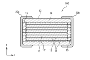
- FIG. 1 is a partial cross-sectional perspective view of a multilayer ceramic capacitor in accordance with a first embodiment.
- FIG. 2 is a cross-sectional view taken along line AA in FIG. 1.
- 2 is a cross-sectional view taken along line BB in FIG. 1.
- FIG. 4 is an enlarged cross-sectional view of the vicinity of an external electrode.
- FIG. 1 illustrates hydrogen transfer.
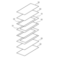
- 1A to 1C are diagrams illustrating a flow of a method for manufacturing a multilayer ceramic capacitor.
- FIG. 1 is a diagram illustrating a lamination process.
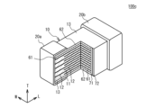
- FIG. FIG. 5 is a partial cross-sectional perspective view of a multilayer ceramic capacitor in accordance with a second embodiment.
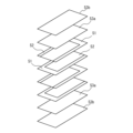
- FIG. 1 is a diagram illustrating a lamination process.
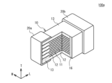
- FIG. 11 is a partial cross-sectional perspective view of a multilayer ceramic capacitor in accordance with a third embodiment.
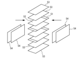
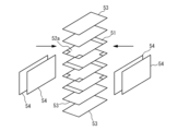
- FIG. 1 is a diagram illustrating a lamination process.
- FIG. 11 is a partial cross-sectional perspective view of a multilayer ceramic capacitor in accordance with a fourth embodiment.
- FIG. 1 is a diagram illustrating a lamination process.
- FIG. 13 is a partial cross-sectional perspective view of a multilayer ceramic capacitor in accordance with a fifth embodiment.
- FIG. 13 is a diagram illustrating the dimension e.
- FIG. 13 is a partial cross-sectional perspective view of a multilayer ceramic capacitor in accordance with a sixth embodiment.
- FIG. 1 is a diagram illustrating a lamination process.
- FIG. 1 is a partially sectional perspective view of a multilayer ceramic capacitor 100 according to the first embodiment.
- FIG. 2 is a cross-sectional view taken along line A-A in FIG. 1.
- FIG. 3 is a cross-sectional view taken along line B-B in FIG. 1.
- the multilayer ceramic capacitor 100 includes a laminated chip 10 having a substantially rectangular parallelepiped shape, and external electrodes 20a, 20b provided on two opposing end faces of the laminated chip 10. Of the four faces of the laminated chip 10 other than the two end faces, the two faces other than the upper and lower faces in the lamination direction are referred to as side faces.
- the external electrodes 20a, 20b extend on the upper, lower and two side faces in the lamination direction of the laminated chip 10. However, the external electrodes 20a and 20b are spaced apart from each other.
- the L direction is the length direction of the laminated chip 10, the direction in which the two end faces of the laminated chip 10 face each other, and the direction in which the external electrodes 20a and 20b face each other.
- the W direction is the width direction of the internal electrode layers, and the direction in which the two side faces other than the two end faces of the four side faces of the laminated chip 10 face each other.
- the T direction is the stacking direction, and the direction in which the top and bottom faces of the laminated chip 10 face each other.
- the L direction, W direction, and T direction are mutually perpendicular.
- the laminated chip 10 has a configuration in which dielectric layers 11 containing a ceramic material that functions as a dielectric and internal electrode layers 12 mainly composed of metal are alternately laminated.
- the laminated chip 10 has a plurality of internal electrode layers 12 facing each other and a dielectric layer 11 sandwiched between the plurality of internal electrode layers 12.
- the edges in the direction in which each internal electrode layer 12 extends are alternately exposed to the first end face on which the external electrode 20a of the laminated chip 10 is provided and the second end face on which the external electrode 20b is provided.
- the internal electrode layer 12 connected to the external electrode 20a is not connected to the external electrode 20b.
- the internal electrode layer 12 connected to the external electrode 20b is not connected to the external electrode 20a.
- each internal electrode layer 12 is alternately conductive to the external electrode 20a and the external electrode 20b.
- the internal electrode layer 12 is disposed on the top layer in the lamination direction, and the internal electrode layer 12 is also disposed on the bottom layer in the lamination direction, and the top and bottom surfaces of the laminate are covered with a cover layer 13.
- the cover layer 13 is mainly composed of a ceramic material.
- the dielectric layer 11 has a main phase of a ceramic material having a perovskite structure represented by the general formula ABO 3.
- the perovskite structure includes ABO 3- ⁇ , which is not a stoichiometric composition.
- the ceramic material can be selected from at least one of BaTiO 3 (barium titanate), CaZrO 3 (calcium zirconate), CaTiO 3 (calcium titanate), SrTiO 3 (strontium titanate), MgTiO 3 (magnesium titanate), Ba 1-x-y Ca x Sr y Ti 1-z Zr z O 3 (0 ⁇ x ⁇ 1, 0 ⁇ y ⁇ 1, 0 ⁇ z ⁇ 1) that forms a perovskite structure, and the like.
- Ba1 -xyCaxSryTi1 - zZrzO3 is barium strontium titanate, barium calcium titanate, barium zirconate, barium zirconate titanate, calcium zirconate titanate and barium calcium zirconate titanate, etc.
- the cover layer 13 has a main phase of a ceramic material having a perovskite structure represented by the general formula ABO 3.
- the perovskite structure includes ABO 3- ⁇ , which is not a stoichiometric composition.
- the ceramic material can be selected from at least one of BaTiO 3 (barium titanate), CaZrO 3 (calcium zirconate), CaTiO 3 (calcium titanate), SrTiO 3 (strontium titanate), MgTiO 3 (magnesium titanate), Ba 1-x-y Ca x Sr y Ti 1-z Zr z O 3 (0 ⁇ x ⁇ 1, 0 ⁇ y ⁇ 1, 0 ⁇ z ⁇ 1) that forms a perovskite structure, and the like.
- Ba1 -x- yCaxSryTi1 - zZrzO3 is barium strontium titanate, barium calcium titanate, barium zirconate, barium zirconate titanate, calcium zirconate titanate, barium calcium zirconate titanate, etc.
- the main component of the cover layer 13 may be the same as or different from that of the dielectric layer 11.
- the dielectric layer 11 and the cover layer 13 may contain additives.
- additives to the dielectric layer 11 and the cover layer 13 include oxides of magnesium (Mg), manganese (Mn), molybdenum (Mo), vanadium (V), chromium (Cr), rare earth elements (yttrium (Y), samarium (Sm), europium (Eu), gadolinium (Gd), terbium (Tb), dysprosium (Dy), holmium (Ho), erbium (Er), thulium (Tm), and ytterbium (Yb)), or oxides containing cobalt (Co), nickel (Ni), lithium (Li), boron (B), sodium (Na), potassium (K), or silicon (Si), or glasses containing Co, Ni, Li, B, Na, K, or Si.
- the main component of the internal electrode layer 12 is a base metal such as Ni, copper (Cu), or tin (Sn), or an alloy containing these.
- the main component of the internal electrode layer 12 may be a precious metal such as platinum (Pt), palladium (Pd), silver (Ag), or gold (Au), or an alloy containing these.
- the region where the internal electrode layer 12 connected to the external electrode 20a and the internal electrode layer 12 connected to the external electrode 20b face each other is a region that generates capacitance in the multilayer ceramic capacitor 100. Therefore, this region that generates capacitance is referred to as the capacitance section 14.
- the capacitance section 14 is a region where adjacent internal electrode layers connected to different external electrodes face each other.
- the region where the internal electrode layers 12 connected to the external electrode 20a face each other without an internal electrode layer 12 connected to the external electrode 20b being interposed therebetween is called the end margin 15.
- the region where the internal electrode layers 12 connected to the external electrode 20b face each other without an internal electrode layer 12 connected to the external electrode 20a being interposed therebetween is also the end margin 15.
- the end margin is the region where the internal electrode layers connected to the same external electrode face each other without an internal electrode layer connected to a different external electrode being interposed therebetween.
- the end margin 15 is a region that does not generate capacitance.
- the end margin 15 may have the same composition as the dielectric layer 11 of the capacitance section 14, or may have a different composition.
- the side margin 16 is a region that is provided to cover the ends of the multiple internal electrode layers 12 that are laminated in the laminated structure and extend to the two side faces.
- the side margin 16 is also a region that does not generate capacitance.
- the side margin 16 may have the same composition as the dielectric layer 11 of the capacitance section 14, or it may have a different composition.
- FIG. 4 is an enlarged cross-sectional view of the vicinity of the external electrode 20a. Hatching is omitted in FIG. 4.
- the external electrode 20a has a structure in which a plating layer 22 is provided on an underlayer 21.
- the underlayer 21 is mainly composed of Ni, Cu, etc.
- the underlayer 21 may contain ceramic particles such as BaTiO 3 as a co-material, or may contain a glass component.
- the plating layer 22 is mainly composed of a metal such as Cu, Ni, aluminum (Al), zinc (Zn), Sn, etc., or an alloy of two or more of these.
- the plating layer 22 may be a plating layer of a single metal component, or may be a plurality of plating layers of different metal components.
- the plating layer 22 has a structure in which a first plating layer 23, a second plating layer 24, and a third plating layer 25 are formed in this order from the underlayer 21 side.
- the first plating layer 23 is, for example, a Cu plating layer.
- the second plating layer 24 is, for example, a Ni plating layer.
- the third plating layer 25 is, for example, a Sn plating layer.
- the external electrode 20a is illustrated in Fig. 4, the external electrode 20b also has a similar layered structure.
- FIG. 5 is a partial cross-sectional perspective view.
- the multilayer ceramic capacitor 100 according to this embodiment has a configuration that can suppress insulation deterioration.
- the cover layer 13 contains an element that forms a covalent hydride by bonding with hydrogen as an additive element.
- the element that forms a covalent hydride is a metal element that easily bonds with hydrogen.
- at least one of Sn, Bi (bismuth), Al, Zn, In (indium), Ga (gallium), and Ge (germanium) can be used as an element that forms a covalent hydride.
- the concentration of the element forming the covalent hydride in the cover layer 13 is small, hydrogen may not be sufficiently retained. Therefore, it is preferable to set a lower limit for the concentration of the element forming the covalent hydride in the cover layer 13.
- the amount of the element forming the covalent hydride in the cover layer 13 is preferably 0.5 at% or more, more preferably 1.0 at% or more, and even more preferably 3.0 at% or more.
- the concentration of the element forming the covalent hydride refers to the amount (at%) of the element forming the covalent hydride when the B site of the perovskite, which is the main component of the cover layer 13, is taken as 100 at%.
- the concentration of the element forming the covalent hydride refers to the total amount of the elements forming the multiple types of covalent hydrides.
- the concentration of the element that forms the covalent hydride in the cover layer 13 is preferably 20 at% or less, more preferably 10 at% or less, and even more preferably 5.0 at% or less.
- the thickness of the cover layer 13 in the T direction is preferably 5 ⁇ m or more, more preferably 10 ⁇ m or more, and even more preferably 15 ⁇ m or more.
- the thickness of the cover layer 13 can be measured by exposing the cross section of the multilayer ceramic capacitor 100, for example, as shown in FIG. 2, by mechanical polishing, and then calculating the average thickness value at 10 locations from an image taken with a microscope such as a scanning transmission electron microscope.
- the thickness of the cover layer 13 in the T direction is preferably 50 ⁇ m or less, more preferably 30 ⁇ m or less, and even more preferably 20 ⁇ m or less.
- the size of the multilayer ceramic capacitor 100 is, for example, 0.25 mm long, 0.125 mm wide, and 0.125 mm high, or 0.4 mm long, 0.2 mm wide, and 0.2 mm high, or 0.6 mm long, 0.3 mm wide, and 0.3 mm high, or 0.6 mm long, 0.3 mm wide, and 0.110 mm high, or 1.0 mm long, 0.5 mm wide, and 0.5 mm high, or 1.0 mm long, 0.5 mm wide, and 0.1 mm high, or 3.2 mm long, 1.6 mm wide, and 1.6 mm high, or 4.5 mm long, 3.2 mm wide, and 2.5 mm high, but is not limited to these sizes.
- each dielectric layer 11 is, for example, 0.3 ⁇ m or more and 3 ⁇ m or less.
- the thickness of each dielectric layer 11 can be measured by exposing the cross section of the multilayer ceramic capacitor 100, for example, as shown in FIG. 2, by mechanical polishing, and then obtaining the average thickness value at 10 points from an image taken by a microscope such as a scanning transmission electron microscope.
- each internal electrode layer 12 is, for example, 0.1 ⁇ m or more and 2 ⁇ m or less.
- the thickness of each internal electrode layer 12 can be measured by exposing the cross section of the multilayer ceramic capacitor 100, for example, as shown in FIG. 2, by mechanical polishing, and then obtaining the average thickness value at 10 points from an image taken by a microscope such as a scanning transmission electron microscope.
- Figure 6 is a diagram illustrating the flow of the method for manufacturing the multilayer ceramic capacitor 100.
- a dielectric material for forming the dielectric layer 11 is prepared.
- the A-site elements and B-site elements contained in the dielectric layer 11 are usually contained in the dielectric layer 11 in the form of a sintered body of ABO3 particles.
- BaTiO3 is a tetragonal compound having a perovskite structure and exhibits a high dielectric constant. This BaTiO3 can generally be obtained by reacting a titanium raw material such as titanium dioxide with a barium raw material such as barium carbonate to synthesize barium titanate.
- a predetermined additive compound is added to the obtained ceramic powder according to the purpose.
- the additive compound may be an oxide of Mg, Mn, Mo, V, Cr, or a rare earth element (Y, Sm, Eu, Gd, Tb, Dy, Ho, Er, Tm, or Yb), or an oxide containing Co, Ni, Li, B, Na, K, or Si, or a glass containing Co, Ni, Li, B, Na, K, or Si.
- SiO2 mainly functions as a sintering aid.
- a compound containing an additive compound is wet mixed with a ceramic raw material powder, and then dried and pulverized to prepare a ceramic material.
- the ceramic material obtained as described above may be pulverized as necessary to adjust the particle size, or may be combined with a classification process to adjust the particle size. Through the above steps, a dielectric material is obtained.
- a binder such as polyvinyl butyral (PVB) resin, an organic solvent such as ethanol or toluene, and a plasticizer are added to the obtained raw material powder and wet mixed.
- a dielectric green sheet is coated on a substrate by, for example, a die coater method or a doctor blade method, and then dried.
- the substrate is, for example, a polyethylene terephthalate (PET) film.
- an internal electrode pattern 52 is formed on a dielectric green sheet 51.
- the dielectric green sheet 51 on which the internal electrode pattern 52 is formed is used as a lamination unit.
- a metal paste of the main component metal of the internal electrode layer 12 is used for the internal electrode pattern 52.
- the film formation method may be printing, sputtering, vapor deposition, etc.
- cover sheets 53 e.g., 2 to 10 layers
- the cover sheet 53 can be formed by the same method as the dielectric green sheet 51. However, an element that forms a covalent bond type hydride is added to the cover sheet 53.
- a re-oxidation treatment may be performed at 600° C. to 1000° C. in a N 2 gas atmosphere.
- a metal paste that will become the underlayer 21 is applied to the first side surface of the laminate by a dipping method or the like.
- This metal paste contains a glass component such as glass frit.
- the metal paste is baked at a temperature of about 700° C. to 900° C. to form the underlayer 21 .
- a metal coating such as copper, nickel, or tin may be applied to the underlayer 21 by a plating process.
- the first plating layer 23, the second plating layer 24, and the third plating layer 25 are formed in this order on the underlayer 21. In this manner, the multilayer ceramic capacitor 100 is completed.
- the elements that form covalent hydrides in the cover layer 13 obtained from the cover sheet 53 which contains elements that form covalent hydrides, suppress the movement of hydrogen. This makes it possible to suppress insulation deterioration.
- the base layer 21 is fired after firing the laminated chip 10, but the base layer 21 may be fired simultaneously when firing the laminated chip 10. Similarly, in the following embodiments, the base layer 21 may be fired simultaneously when firing the laminated chip 10.
- a low-melting point metal such as an element that forms the above-mentioned covalent bond type hydride is disposed in the internal electrode layer 12 or at the interface between the internal electrode layer 12 and the dielectric layer 11, diffusion from the external electrodes 20a, 20b may be promoted.
- FIG. 9 is a partial cross-sectional perspective view of a multilayer ceramic capacitor 100a according to the second embodiment.
- the cover layer 13 includes an inner layer 61 located on the side of the capacitance section 14 in the T direction, and an outer layer 62 located on the opposite side of the capacitance section 14 in the T direction.
- the concentration of the element that forms the covalent hydride is higher in the outer layer 62 than in the inner layer 61.
- the concentration of the element that forms the covalent hydride in the inner layer 61 is reduced. This reduces the amount of the element that forms the covalent hydride in the internal electrode layer 12 or at the interface between the internal electrode layer 12 and the dielectric layer 11. This suppresses diffusion from the external electrodes 20a, 20b to the internal electrode layer 12, and suppresses the occurrence of cracks 40.
- the additive concentration of the element that forms the covalent hydride in the outer layer 62 can be, for example, the same as the additive concentration in the cover layer 13 of the first embodiment.
- the additive concentration of the element that forms the covalent hydride in the inner layer 61 may be lower than the additive concentration of the element that forms the covalent hydride in the outer layer 62, but it is preferable that the inner layer 61 does not contain any element that forms a covalent hydride.
- the thickness ratio of the inner layer 61 and the outer layer 62 is not particularly limited, but is, for example, about 1:1. In other words, when the cover layer 13 is divided in half at the center in the thickness direction, the concentration of the element that forms the covalent bond type hydride may be higher on the side farther from the internal electrode layer 12 than on the side closer to the internal electrode layer 12.
- the concentration of the element that forms the covalent hydride in the cover sheet 53a that is close to the laminate of the dielectric green sheets 51 on which the internal electrode patterns 52 are formed may be lower than the concentration of the element that forms the covalent hydride in the cover sheet 53b that is farther from the laminate.
- FIG. 11 is a partial cross-sectional perspective view of a multilayer ceramic capacitor 100b according to a third embodiment.
- the side margin 16 in addition to the cover layer 13, also contains an element that forms a covalent hydride.
- the side margin 16 contains an element that forms a covalent hydride, even if hydrogen stored in the plating layer moves toward the internal electrode layer 12, the hydrogen is held by the element that forms the covalent hydride contained in the side margin 16, and the movement of hydrogen to the internal electrode layer 12 is suppressed. This makes it possible to suppress insulation deterioration.
- the additive concentration of the element that forms the covalent hydride in the side margin 16 can be, for example, the same as the additive concentration in the cover layer 13 of the first embodiment.
- the multilayer ceramic capacitor 100b according to this embodiment can be fabricated as shown in FIG. 12.
- an internal electrode pattern 52 is formed on a dielectric green sheet 51 to form a laminate unit.
- the laminate units are laminated in order.
- the width in the W direction of the internal electrode pattern 52 is made to match the width in the W direction of the dielectric green sheet 51.
- a predetermined number of cover sheets 53 e.g., 2 to 10 layers
- cover sheets 53 e.g., 2 to 10 layers
- a plurality of side margin sheets 54 are attached to each of both side surfaces of the laminate.
- the side margin sheets 54 can be formed by the same method as the dielectric green sheet 51. However, an element that forms a covalent bond type hydride is added to the side margin sheets 54.
- FIG. 13 is a partial cross-sectional perspective view of a multilayer ceramic capacitor 100c according to a fourth embodiment.
- the side margin 16 includes an inner layer 71 located on the side of the capacitance section 14 in the W direction, and an outer layer 72 located on the opposite side of the capacitance section 14 in the W direction.
- the concentration of the element that forms the covalent hydride is higher in the outer layer 72 than in the inner layer 71.
- the concentration of the element that forms the covalent hydride in the inner layer 71 is reduced. This reduces the amount of the element that forms the covalent hydride in the internal electrode layer 12 or at the interface between the internal electrode layer 12 and the dielectric layer 11. This suppresses diffusion from the external electrodes 20a, 20b to the internal electrode layer 12, and suppresses the occurrence of cracks 40.
- the additive concentration of the element that forms the covalent hydride in the outer layer 72 can be, for example, the same as the additive concentration in the cover layer 13 of the first embodiment.
- the additive concentration of the element that forms the covalent hydride in the inner layer 71 may be lower than the additive concentration of the element that forms the covalent hydride in the outer layer 72, but it is preferable that the inner layer 71 does not contain any element that forms a covalent hydride.
- the thickness ratio of the inner layer 71 and the outer layer 72 is not particularly limited, but is, for example, about 1:1. In other words, when the side margin 16 is divided in half at the center in the W direction, the concentration of the element that forms the covalent bond type hydride may be higher on the side farther from the internal electrode layer 12 than on the side closer to the internal electrode layer 12.
- the concentration of the element that forms the covalent hydride in the side margin sheet 54a close to the laminate of the dielectric green sheets 51 on which the internal electrode pattern 52 is formed may be lower than the concentration of the element that forms the covalent hydride in the side margin sheet 54b farther from the laminate.
- the width of the internal electrode layer 12 is changed.
- the internal electrode layer 12 connected to the external electrode 20a has a first region 121 (connection portion) connected to the external electrode 20a in a region corresponding to the end margin 15 and having a width W1, and a second region 122 in a region corresponding to the capacitance portion 14 and having a width W2.
- the width W1 is smaller than the width W2.
- the width W1 and the width W2 refer to the width in the W direction.
- the movement distance from the external electrodes 20a, 20b to the internal electrode layer 12 is long at the corner portion, so that the diffusion from the external electrodes 20a, 20b to the internal electrode layer 12 is suppressed. As a result, the occurrence of cracks 40 is suppressed.
- the internal electrode layer 12 connected to the external electrode 20b also has a first region 121 having a width W1 and a second region 122 having a width W2.
- W1/W2 is preferably 1/2 or more, and more preferably 2/3 or more. Also, W1/W2 is preferably 4/5 or less, and more preferably 3/4 or less.
- the dimension of the external electrodes 20a, 20b extending in the L direction from both end faces of the laminated chip 10 is referred to as dimension e.
- the dimension of the first region 121 in the L direction is 1/3 or more of dimension e, and more preferably 1/2 or more.
- the laminated chip 10 it is sufficient that at least some of the internal electrode layers 12 have the first region 121 and the second region 122 as described above, but it is preferable that the outermost internal electrode layer 12 has the first region 121 and the second region 122. For example, it is preferable that 5% to 25% of the total number of layers from each outermost layer have the first region 121 and the second region 122.
- the multilayer ceramic capacitor 100d according to this embodiment can be obtained, for example, by stacking dielectric green sheets 51 on which internal electrode patterns 52a having widths W1 and W2 are formed, as illustrated in FIG. 17.
- the multilayer ceramic capacitor 100e according to the sixth embodiment has a configuration in which the internal electrode layer 12 having the width W1 and the width W2 is applied to the third embodiment.
- the side margin 16 contains an element that forms a covalent bond type hydride, even if hydrogen occluded in the plating layer moves toward the internal electrode layer 12, the hydrogen is held by the element that forms the covalent bond type hydride contained in the side margin 16, and the movement of the hydrogen to the internal electrode layer 12 is suppressed. This makes it possible to suppress insulation deterioration.
- the multilayer ceramic capacitor 100b according to this embodiment can be fabricated as shown in FIG. 19.
- an internal electrode pattern 52a having widths W1 and W2 is formed on a dielectric green sheet 51 to form a laminate unit.
- the laminate units are laminated in order.
- the width W2 is made to match the width of the dielectric green sheet 51 in the W direction.
- a predetermined number of cover sheets 53 e.g., 2 to 10 layers
- cover sheets 53 e.g., 2 to 10 layers
- a plurality of side margin sheets 54 are attached to each of both side surfaces of the laminate.
- the side margin sheets 54 can be formed by the same method as the dielectric green sheet 51. However, an element that forms a covalent bond type hydride is added to the side margin sheets 54.
- a multilayer ceramic capacitor has been described as an example of a ceramic electronic component, but the present invention is not limited to this.
- the configuration of each of the above embodiments can also be applied to other multilayer ceramic electronic components, such as varistors and thermistors.
- the multilayer ceramic capacitors according to each embodiment were fabricated and their characteristics were investigated.
- Example 1 the multilayer ceramic capacitor described in the first embodiment was produced. First, a slurry mainly composed of BaTiO3 was mixed and coated to obtain a dielectric green sheet. An internal electrode pattern was printed on each dielectric green sheet. Nickel powder was used for the internal electrode pattern. In the W direction, the width of each internal electrode pattern was made smaller than the width of the dielectric green sheet. 260 layers of the obtained laminate unit were laminated to obtain a laminate.
- a slurry mainly composed of BaTiO 3 was mixed and applied to obtain a cover sheet.
- 1.0 at % Sn was added to the cover sheet as an element forming a covalent bond type hydride.
- a plurality of cover sheets were laminated and pressed on the top and bottom of the stacking direction of the above-mentioned laminate, and then a binder removal process was performed. Then, the laminate was fired and reoxidized.
- a metal paste mainly composed of Cu was applied to two end faces of the obtained laminated chip and baked at about 800 ° C. Through these processes, a multilayer ceramic capacitor with 260 internal electrode layers was produced in a 0603 shape (length L: 0.6 mm, width W: 0.3 mm, height T: 0.3 mm).
- each internal electrode layer was 0.5 ⁇ m, and the thickness of each dielectric layer was 0.5 ⁇ m.
- the thickness of each cover layer in the T direction was 20 ⁇ m.
- the thickness of each side margin in the W direction was 20 ⁇ m.
- the length of each end margin in the L direction was 40 ⁇ m.
- the dimension e of each external electrode extending in the L direction from both end faces of the multilayer chip was 120 ⁇ m.
- Example 2 In Example 2, the multilayer ceramic capacitor described in the second embodiment was produced. In Example 2, in each cover layer, Sn was not added to the cover sheet in the portion corresponding to 10 ⁇ m on the capacitance part side (inside) in the T direction, and Sn was added to the cover sheet in the portion corresponding to 10 ⁇ m on the opposite side (outside) in the T direction at 2.0 at %. Other conditions were the same as in Example 1.
- Example 3 In Example 3, a multilayer ceramic capacitor was produced as described in the third embodiment. In Example 3, the width of the internal electrode pattern and the width of the dielectric green sheet were made the same in the W direction of the laminate of the laminate unit.
- a slurry mainly composed of BaTiO3 was mixed and coated to obtain a side margin sheet.
- 1.0 at% Sn was added to the side margin sheet.
- a plurality of side margin sheets were attached to both ends of the laminate in the W direction of the laminate unit, and then the binder removal process was performed. Then, the laminate was fired and reoxidized.
- the other conditions were the same as in Example 1.
- Example 4 In Example 4, a multilayer ceramic capacitor was produced as described in the fourth embodiment. In Example 4, the width of the internal electrode pattern and the width of the dielectric green sheet were made the same in the W direction of the laminate of the laminate unit.
- a slurry mainly composed of BaTiO3 was mixed and coated to obtain a side margin sheet. 2.0 at% Sn was added to the side margin sheet. A plurality of side margin sheets were attached to both ends of the laminate in the W direction of the laminate unit, and then the binder removal process was performed. Then, the laminate was fired and reoxidized.
- Example 4 no Sn was added to the side margin sheet in the portion corresponding to 10 ⁇ m on the capacitance side (inner side) in the W direction for each side margin, and 2.0 at% Sn was added to the side margin sheet in the portion corresponding to 10 ⁇ m on the opposite side (outer side) in the W direction.
- the other conditions were the same as in Example 2.
- Example 5 the multilayer ceramic capacitor described in the fifth embodiment was fabricated.
- the width W2 in the W direction was increased in the capacitance section, and the width W1 in the W direction was decreased in the end margin.
- the width W2 of the internal electrode layer in the capacitance section was 260 ⁇ m, and the width W2 of the internal electrode layer in the end margin was 220 ⁇ m.
- the other conditions were the same as in Example 1.
- Example 6 the multilayer ceramic capacitor described in the fifth embodiment was fabricated.
- the width W2 in the W direction was increased in the capacitance section, and the width W1 in the W direction was decreased in the end margin.
- the width W2 of the internal electrode layer in the capacitance section was 260 ⁇ m, and the width W1 of the internal electrode layer in the end margin was 220 ⁇ m.
- the other conditions were the same as in Example 3.
- Table 1 shows the conditions for Examples 1 to 6 and the Comparative Example.
Landscapes
- Engineering & Computer Science (AREA)
- Power Engineering (AREA)
- Manufacturing & Machinery (AREA)
- Microelectronics & Electronic Packaging (AREA)
- Ceramic Capacitors (AREA)
- Fixed Capacitors And Capacitor Manufacturing Machines (AREA)
Abstract
セラミックを主成分とする2層のカバー層の間で、複数の誘電体層と複数の内部電極層とが交互に積層され、略直方体形状を有し、前記略直方体形状の対向する第1端面と第2端面とに前記複数の内部電極層が交互に露出するように形成された積層チップと、前記1端面および前記第2端面に設けられ、下地層上にめっき層が設けられた1対の外部電極と、を備え、前記1対の外部電極のそれぞれは、前記積層チップの積層方向の上面および下面の少なくともいずれか一方まで延在し、前記カバー層は、共有結合型水素化物を形成する元素のうち少なくとも1種の添加元素を含むことを特徴とする。
Description
本発明は、セラミック電子部品およびその製造方法に関する。
近年、電気自動車等の分野で、積層セラミックコンデンサなどの信頼性の高いセラミック電子部品が求められている。
外部電極の表面にめっき層を形成する場合において、めっき工程において発生した水素がめっき層中に吸蔵される。この場合、外部電極に電圧が印加されると、めっき層から容量部に向かって水素が移動する。移動する水素が内部電極層に到達すると、絶縁劣化が引き起こされる。そこで、めっき層と内部電極層との間に、水素を捕捉するためのダミー層を有する構造が提案されている(特許文献1)。
しかしながら、このような手法によると、ダミー層の印刷や積層に位置ズレが生じた場合、水素の補足が不十分となり、絶縁抵抗が劣化するおそれがある。
本発明は、上記課題に鑑みなされたものであり、絶縁抵抗の劣化を抑制することができるセラミック電子部品およびその製造方法を提供することを目的とする。
本発明に係るセラミック電子部品は、セラミックを主成分とする2層のカバー層の間で、複数の誘電体層と複数の内部電極層とが交互に積層され、略直方体形状を有し、前記略直方体形状の対向する第1端面と第2端面とに前記複数の内部電極層が交互に露出するように形成された積層チップと、前記1端面および前記第2端面に設けられ、下地層上にめっき層が設けられた1対の外部電極と、を備え、前記1対の外部電極のそれぞれは、前記積層チップの積層方向の上面および下面の少なくともいずれか一方まで延在し、前記カバー層は、共有結合型水素化物を形成する元素のうち少なくとも1種の添加元素を含むことを特徴とする。
上記セラミック電子部品において、前記添加元素は、Sn、Bi、In、Gaのいずれか1つを含んでいてもよい。
上記セラミック電子部品において、前記カバー層を厚み方向の中央で半分に分けた場合に、前記添加元素の濃度は、前記内部電極層に近い側よりも前記内部電極層から遠い側の方が高くてもよい。
上記セラミック電子部品において、前記積層チップは、前記上面、前記下面、前記第1端面、および前記第2端面以外の2側面から前記複数の内部電極層に至るまでのサイドマージンを備え、前記サイドマージンは、セラミックを主成分とし、前記添加元素を含んでいてもよい。
上記セラミック電子部品において、前記サイドマージンを、前記2側面が対向する方向の中央で半分に分けた場合に、前記添加元素の濃度は、前記内部電極層に近い側よりも前記内部電極層から遠い側の方が高くてもよい。
上記セラミック電子部品の前記複数の内部電極層のうち最外層の内部電極層において、前記外部電極に接続される接続部の幅が、他の幅よりも狭くてもよい。
上記セラミック電子部品において、前記複数の内部電極層のうち、最外層から全層数の5%~25%の層数の内部電極層において、前記外部電極に接続される接続部の幅が、他の幅よりも狭くてもよい。
上記セラミック電子部品において、前記接続部の幅は、異なる外部電極に接続される内部電極層同士が対向する領域における前記内部電極層の幅の、1/2以上、4/5以下であってもよい。
上記セラミック電子部品において、前記めっき層は、Niを主成分としてもよい。
上記セラミック電子部品において、前記下地層は、Cuを主成分としてもよい。
上記セラミック電子部品において、前記めっき層の外側に、Snめっき層が設けられていてもよい。
本発明に係るセラミック電子部品の製造方法は、セラミックを主成分とする2層のカバー層の間で、複数の誘電体層と複数の内部電極層とが交互に積層され、略直方体形状を有し、前記略直方体形状の対向する第1端面と第2端面とに前記複数の内部電極層が交互に露出するように形成された積層チップと、前記1端面および前記第2端面に設けられ前記積層チップの積層方向の上面および下面の少なくともいずれか一方まで延在する下地層と、を備える中間体を準備する工程と、前記下地層上にめっき層を形成する工程と、を含み、前記カバー層は、共有結合型水素化物を形成する元素のうち少なくとも1種の添加元素を含むことを特徴とする。
本発明によれば、絶縁抵抗の劣化を抑制することができるセラミック電子部品およびその製造方法を提供することができる。
以下、図面を参照しつつ、実施形態について説明する。
(第1実施形態)
図1は、第1実施形態に係る積層セラミックコンデンサ100の部分断面斜視図である。図2は、図1のA-A線断面図である。図3は、図1のB-B線断面図である。図1~図3で例示するように、積層セラミックコンデンサ100は、略直方体形状を有する積層チップ10と、積層チップ10のいずれかの対向する2端面に設けられた外部電極20a,20bと、を備える。なお、積層チップ10の当該2端面以外の4面のうち、積層方向の上面および下面以外の2面を側面と称する。外部電極20a,20bは、積層チップ10の積層方向の上面、下面および2側面に延在している。ただし、外部電極20aと外部電極20bとは、互いに離間している。
図1は、第1実施形態に係る積層セラミックコンデンサ100の部分断面斜視図である。図2は、図1のA-A線断面図である。図3は、図1のB-B線断面図である。図1~図3で例示するように、積層セラミックコンデンサ100は、略直方体形状を有する積層チップ10と、積層チップ10のいずれかの対向する2端面に設けられた外部電極20a,20bと、を備える。なお、積層チップ10の当該2端面以外の4面のうち、積層方向の上面および下面以外の2面を側面と称する。外部電極20a,20bは、積層チップ10の積層方向の上面、下面および2側面に延在している。ただし、外部電極20aと外部電極20bとは、互いに離間している。
なお、図1~図3において、L方向は、積層チップ10の長さ方向であって、積層チップ10の2端面が対向する方向であり、外部電極20aと外部電極20bとが対向する方向である。W方向は、内部電極層の幅方向であり、積層チップ10の4側面のうち2端面以外の2側面が対向する方向である。T方向は、積層方向であり、積層チップ10の上面と下面とが対向する方向である。L方向と、W方向と、T方向とは、互いに直交している。
積層チップ10は、誘電体として機能するセラミック材料を含む誘電体層11と、金属を主成分とする内部電極層12とが、交互に積層された構成を有する。言い換えると、積層チップ10は、互いに対向する複数の内部電極層12と、複数の内部電極層12の間に各々挟まれた誘電体層11と、を備えている。各内部電極層12が延伸される方向の端縁は、積層チップ10の外部電極20aが設けられた第1端面と、外部電極20bが設けられた第2端面とに対して、交互に露出している。外部電極20aに接続される内部電極層12は、外部電極20bには接続されていない。外部電極20bに接続される内部電極層12は、外部電極20aには接続されていない。したがって、各内部電極層12が、外部電極20aと外部電極20bとに、交互に導通する。また、誘電体層11と内部電極層12との積層体において、積層方向の最上層には内部電極層12が配置され、積層方向の最下層にも内部電極層12が配置され、当該積層体の上面および下面は、カバー層13によって覆われている。カバー層13は、セラミック材料を主成分とする。
誘電体層11は、例えば、一般式ABO3で表されるペロブスカイト構造を有するセラミック材料を主相とする。なお、当該ペロブスカイト構造は、化学量論組成から外れたABO3-αを含む。例えば、当該セラミック材料として、BaTiO3(チタン酸バリウム),CaZrO3(ジルコン酸カルシウム),CaTiO3(チタン酸カルシウム),SrTiO3(チタン酸ストロンチウム),MgTiO3(チタン酸マグネシウム),ペロブスカイト構造を形成するBa1-x-yCaxSryTi1-zZrzO3(0≦x≦1,0≦y≦1,0≦z≦1)等のうち少なくとも1つから選択して用いることができる。Ba1-x-yCaxSryTi1-zZrzO3は、チタン酸バリウムストロンチウム、チタン酸バリウムカルシウム、ジルコン酸バリウム、チタン酸ジルコン酸バリウム、チタン酸ジルコン酸カルシウムおよびチタン酸ジルコン酸バリウムカルシウムなどである。
カバー層13は、例えば、一般式ABO3で表されるペロブスカイト構造を有するセラミック材料を主相とする。なお、当該ペロブスカイト構造は、化学量論組成から外れたABO3-αを含む。例えば、当該セラミック材料として、BaTiO3(チタン酸バリウム),CaZrO3(ジルコン酸カルシウム),CaTiO3(チタン酸カルシウム),SrTiO3(チタン酸ストロンチウム),MgTiO3(チタン酸マグネシウム),ペロブスカイト構造を形成するBa1-x-yCaxSryTi1-zZrzO3(0≦x≦1,0≦y≦1,0≦z≦1)等のうち少なくとも1つから選択して用いることができる。Ba1-x-yCaxSryTi1-zZrzO3は、チタン酸バリウムストロンチウム、チタン酸バリウムカルシウム、ジルコン酸バリウム、チタン酸ジルコン酸バリウム、チタン酸ジルコン酸カルシウムおよびチタン酸ジルコン酸バリウムカルシウムなどである。カバー層13は、主成分が誘電体層11と同じであってもよく、異なっていてもよい。
誘電体層11およびカバー層13には、添加物が添加されていてもよい。誘電体層11およびカバー層13への添加物として、マグネシウム(Mg)、マンガン(Mn)、モリブデン(Mo)、バナジウム(V)、クロム(Cr)、希土類元素(イットリウム(Y)、サマリウム(Sm)、ユーロピウム(Eu)、ガドリニウム(Gd)、テルビウム(Tb)、ジスプロシウム(Dy)、ホルミウム(Ho)、エルビウム(Er)、ツリウム(Tm)およびイッテルビウム(Yb))の酸化物、または、コバルト(Co)、ニッケル(Ni)、リチウム(Li)、ホウ素(B)、ナトリウム(Na)、カリウム(K)もしくはケイ素(Si)を含む酸化物、または、Co、Ni、Li、B、Na、KもしくはSiを含むガラスが挙げられる。
内部電極層12は、Ni,銅(Cu),スズ(Sn)等の卑金属やこれらを含む合金を主成分とする。内部電極層12の主成分として、白金(Pt),パラジウム(Pd),銀(Ag),金(Au)などの貴金属やこれらを含む合金を主成分として用いてもよい。
図2で例示するように、外部電極20aに接続された内部電極層12と外部電極20bに接続された内部電極層12とが対向する領域は、積層セラミックコンデンサ100において静電容量を生じる領域である。そこで、当該静電容量を生じる領域を、容量部14と称する。すなわち、容量部14は、異なる外部電極に接続された隣接する内部電極層同士が対向する領域である。
外部電極20aに接続された内部電極層12同士が、外部電極20bに接続された内部電極層12を介さずに対向する領域を、エンドマージン15と称する。また、外部電極20bに接続された内部電極層12同士が、外部電極20aに接続された内部電極層12を介さずに対向する領域も、エンドマージン15である。すなわち、エンドマージンは、同じ外部電極に接続された内部電極層が異なる外部電極に接続された内部電極層を介さずに対向する領域である。エンドマージン15は、静電容量を生じない領域である。エンドマージン15は、容量部14の誘電体層11と同じ組成であってもよく、異なる組成であってもよい。
図3で例示するように、積層チップ10において、積層チップ10の2側面から内部電極層12に至るまでの領域をサイドマージン16と称する。すなわち、サイドマージン16は、上記積層構造において積層された複数の内部電極層12が2側面側に延びた端部を覆うように設けられた領域である。サイドマージン16も、静電容量を生じない領域である。サイドマージン16は、容量部14の誘電体層11と同じ組成であってもよく、異なる組成であってもよい。
図4は、外部電極20a付近の拡大断面図である。図4では、ハッチを省略している。図4で例示するように、外部電極20aは、下地層21上に、めっき層22が設けられた構造を有している。下地層21は、Ni、Cuなどを主成分とする。下地層21は、BaTiO3などのセラミック粒子を共材として含んでいてもよく、ガラス成分を含んでいてもよい。めっき層22は、Cu、Ni、アルミニウム(Al)、亜鉛(Zn)、Snなどの金属またはこれらの2以上の合金を主成分とする。めっき層22は、単一金属成分のめっき層でもよく、互いに異なる金属成分の複数のめっき層でもよい。例えば、めっき層22は、下地層21側から順に、第1めっき層23、第2めっき層24および第3めっき層25が形成された構造を有する。第1めっき層23は、例えば、Cuめっき層である。第2めっき層24は、例えば、Niめっき層である。第3めっき層25は、例えば、Snめっき層である。なお、図4では、外部電極20aについて例示しているが、外部電極20bも同様の積層構造を有する。
このようにめっき層を有する積層セラミックコンデンサにおいては、めっき工程で発生した水素がめっき層に吸蔵される。回路基板上で外部電極に電圧が印加されると、図5で例示するように、めっき層を備える外部電極20a,20bから容量部の内部電極層12に向かって水素が移動する。移動する水素が内部電極層12に到達すると、絶縁劣化が引き起こされる。そこで、めっき層と内部電極層との間に、水素を捕捉するためのダミー層を有する構造が提案されている。しかしながら、このような手法によると、ダミー層の印刷や積層に位置ズレが生じた場合、水素の補足が不十分となり、絶縁劣化が生じるおそれがある。なお、図5は、部分断面斜視図である。
特に、めっき工程でNiめっき層を形成する場合には、水素がNiめっき層内に吸蔵されやすい。また、水素が吸蔵されているめっき層よりも外側にSnめっき層が形成されていると、最密充填構造を有するSnが水素の通り道を塞ぐため、Snめっき層よりも内側に水素が閉じ込められる傾向にある。したがって、外部電極において、Niめっき層が形成されており、当該Niめっき層よりも外側にSnめっき層が形成されている構造において、特に絶縁劣化が問題になり得る。
そこで、本実施形態に係る積層セラミックコンデンサ100は、絶縁劣化を抑制することができる構成を有している。
具体的には、カバー層13は、水素と結合することで共有結合型水素化物を形成する元素を添加元素として含んでいる。共有結合型水素化物を形成する元素は、水素と結合しやすい金属元素である。例えば、共有結合型水素化物を形成する元素として、Sn、Bi(ビスマス)、Al、Zn、In(インジウム)、Ga(ガリウム)、およびGe(ゲルマニウム)の少なくとも1種以上を用いることができる。カバー層13が共有結合型水素化物を形成する元素を含むことで、めっき層に吸蔵されている水素が内部電極層12に向かって移動しても、カバー層13内で共有結合型水素化物を形成する元素によって保持されるため、内部電極層12への水素の移動が抑制される。それにより、絶縁劣化を抑制することができる。
カバー層13において、共有結合型水素化物を形成する元素の添加濃度が小さいと、十分に水素が保持されないおそれがある。そこで、カバー層13において、共有結合型水素化物を形成する元素の添加濃度に下限を設けることが好ましい。本実施形態においては、カバー層13において、共有結合型水素化物を形成する元素の添加濃度量は、0.5at%以上であることが好ましく、1.0at%以上であることがより好ましく、3.0at%以上であることがさらに好ましい。なお、共有結合型水素化物を形成する元素の添加濃度は、カバー層13の主成分のペロブスカイトのBサイトを100at%とした場合の共有結合型水素化物を形成する元素の量(at%)のことである。複数種類の共有結合型水素化物を形成する元素が含まれる場合には、共有結合型水素化物を形成する元素の添加濃度は、当該複数種類の共有結合型水素化物を形成する元素の合計量のことである。
一方、カバー層13において、共有結合型水素化物を形成する元素の添加濃度が高いと、異常な粒成長を引き起こすおそれがある。そこで、カバー層13において、共有結合型水素化物を形成する元素の添加濃度に上限を設けることが好ましい。本実施形態においては、カバー層13において、共有結合型水素化物を形成する元素の添加濃度は、20at%以下であることが好ましく、10at%以下であることがより好ましく、5.0at%以下であることがさらに好ましい。
T方向におけるカバー層13の厚みが小さいと、耐湿性が不足するおそれがある。そこで、T方向におけるカバー層13の厚みに下限を設けることが好ましい。本実施形態においては、T方向におけるカバー層13の厚みは、5μm以上であることが好ましく、10μm以上であることがより好ましく、15μm以上であることがさらに好ましい。カバー層13の厚みは、積層セラミックコンデンサ100の例えば図2の断面を機械研磨で露出した後、走査透過電子顕微鏡等の顕微鏡で撮影した画像から10か所の厚さの平均値を求めるようにして測定することができる。
一方、T方向におけるカバー層13の厚みが大きいと、容量部14が十分に確保できなくなるおそれがある。そこで、T方向におけるカバー層13の厚みに上限を設けることが好ましい。本実施形態においては、T方向におけるカバー層13の厚みは、50μm以下であることが好ましく、30μm以下であることがより好ましく、20μm以下であることがさらに好ましい。
積層セラミックコンデンサ100のサイズは、例えば、長さ0.25mm、幅0.125mm、高さ0.125mmであり、または長さ0.4mm、幅0.2mm、高さ0.2mm、または長さ0.6mm、幅0.3mm、高さ0.3mmであり、または長さ0.6mm、幅0.3mm、高さ0.110mmであり、または長さ1.0mm、幅0.5mm、高さ0.5mmであり、または長さ1.0mm、幅0.5mm、高さ0.1mmであり、または長さ3.2mm、幅1.6mm、高さ1.6mmであり、または長さ4.5mm、幅3.2mm、高さ2.5mmであるが、これらのサイズに限定されるものではない。
1層あたりの誘電体層11の厚みは、例えば、0.3μm以上3μm以下である。1層あたりの誘電体層11の厚みは、積層セラミックコンデンサ100の例えば図2の断面を機械研磨で露出した後、走査透過電子顕微鏡等の顕微鏡で撮影した画像から10か所の厚さの平均値を求めるようにして測定することができる。
1層あたりの内部電極層12の厚みは、例えば、0.1μm以上2μm以下である。1層あたりの内部電極層12の厚みは、積層セラミックコンデンサ100の例えば図2の断面を機械研磨で露出した後、走査透過電子顕微鏡等の顕微鏡で撮影した画像から10か所の厚さの平均値を求めるようにして測定することができる。
続いて、第1実施形態に係る積層セラミックコンデンサ100の製造方法について説明する。図6は、積層セラミックコンデンサ100の製造方法のフローを例示する図である。
(原料粉末作製工程)
まず、誘電体層11を形成するための誘電体材料を用意する。誘電体層11に含まれるAサイト元素およびBサイト元素は、通常はABO3の粒子の焼結体の形で誘電体層11に含まれる。例えば、BaTiO3は、ペロブスカイト構造を有する正方晶化合物であって、高い誘電率を示す。このBaTiO3は、一般的に、二酸化チタンなどのチタン原料と炭酸バリウムなどのバリウム原料とを反応させてチタン酸バリウムを合成することで得ることができる。誘電体層11の主成分セラミックの合成方法としては、従来種々の方法が知られており、例えば固相法、ゾル-ゲル法、水熱法等が知られている。本実施形態においては、これらのいずれも採用することができる。
まず、誘電体層11を形成するための誘電体材料を用意する。誘電体層11に含まれるAサイト元素およびBサイト元素は、通常はABO3の粒子の焼結体の形で誘電体層11に含まれる。例えば、BaTiO3は、ペロブスカイト構造を有する正方晶化合物であって、高い誘電率を示す。このBaTiO3は、一般的に、二酸化チタンなどのチタン原料と炭酸バリウムなどのバリウム原料とを反応させてチタン酸バリウムを合成することで得ることができる。誘電体層11の主成分セラミックの合成方法としては、従来種々の方法が知られており、例えば固相法、ゾル-ゲル法、水熱法等が知られている。本実施形態においては、これらのいずれも採用することができる。
得られたセラミック粉末に、目的に応じて所定の添加化合物を添加する。添加化合物としては、Mg、Mn、Mo、V、Cr、希土類元素(Y、Sm、Eu、Gd、Tb、Dy、Ho、Er、TmおよびYb)の酸化物、または、Co、Ni、Li、B、Na、KもしくはSiを含む酸化物、または、Co、Ni、Li、B、Na、KもしくはSiを含むガラスが挙げられる。これらのうち、主としてSiO2が焼結助剤として機能する。
例えば、セラミック原料粉末に添加化合物を含む化合物を湿式混合し、乾燥および粉砕してセラミック材料を調製する。例えば、上記のようにして得られたセラミック材料について、必要に応じて粉砕処理して粒径を調節し、あるいは分級処理と組み合わせることで粒径を整えてもよい。以上の工程により、誘電体材料が得られる。
(積層工程)
次に、得られた原料粉末に、ポリビニルブチラール(PVB)樹脂等のバインダと、エタノール、トルエン等の有機溶剤と、可塑剤とを加えて湿式混合する。得られたスラリを使用して、例えばダイコータ法やドクターブレード法により、基材上に誘電体グリーンシートを塗工して乾燥させる。基材は、例えば、ポリエチレンテレフタレート(PET)フィルムである。
次に、得られた原料粉末に、ポリビニルブチラール(PVB)樹脂等のバインダと、エタノール、トルエン等の有機溶剤と、可塑剤とを加えて湿式混合する。得られたスラリを使用して、例えばダイコータ法やドクターブレード法により、基材上に誘電体グリーンシートを塗工して乾燥させる。基材は、例えば、ポリエチレンテレフタレート(PET)フィルムである。
次に、図7で例示するように、誘電体グリーンシート51上に、内部電極パターン52を成膜する。内部電極パターン52が成膜された誘電体グリーンシート51を、積層単位とする。内部電極パターン52には、内部電極層12の主成分金属の金属ペーストを用いる。成膜の手法は、印刷、スパッタ、蒸着などであってもよい。
次に、誘電体グリーンシート51を基材から剥がしつつ、図7で例示するように、積層単位を積層する。次に、積層単位が積層されることで得られた積層体の上下にカバーシート53を所定数(例えば2~10層)だけ積層して熱圧着する。カバーシート53は、誘電体グリーンシート51と同様の手法により形成することができる。ただし、カバーシート53には、共有結合型水素化物を形成する元素を添加する。
(焼成工程)
その後、酸素分圧10-5~10-8atmの還元雰囲気中で1100~1300℃で10分~2時間焼成する。
その後、酸素分圧10-5~10-8atmの還元雰囲気中で1100~1300℃で10分~2時間焼成する。
(再酸化処理工程)
その後、N2ガス雰囲気中において600℃~1000℃で再酸化処理を行ってもよい。
その後、N2ガス雰囲気中において600℃~1000℃で再酸化処理を行ってもよい。
(塗布工程)
次に、積層体の第1側面に、下地層21となる金属ペーストをディップ法などで塗布する。この金属ペーストには、ガラスフリットなどのガラス成分を含ませる。
次に、積層体の第1側面に、下地層21となる金属ペーストをディップ法などで塗布する。この金属ペーストには、ガラスフリットなどのガラス成分を含ませる。
(焼付工程)
次に、700℃~900℃程度の温度で金属ペーストを焼き付けることで、下地層21を形成する。
次に、700℃~900℃程度の温度で金属ペーストを焼き付けることで、下地層21を形成する。
(めっき処理工程)
その後、めっき処理により、下地層21上に、銅、ニッケル、スズ等の金属コーティングを行ってもよい。例えば、下地層21上に、第1めっき層23、第2めっき層24および第3めっき層25を順に形成する。それにより、積層セラミックコンデンサ100が完成する。
その後、めっき処理により、下地層21上に、銅、ニッケル、スズ等の金属コーティングを行ってもよい。例えば、下地層21上に、第1めっき層23、第2めっき層24および第3めっき層25を順に形成する。それにより、積層セラミックコンデンサ100が完成する。
本実施形態に係る製造方法によれば、めっき処理工程でめっき層に水素が吸蔵されるおそれがあるものの、共有結合型水素化物を形成する元素を含むカバーシート53から得られるカバー層13内の共有結合型水素化物を形成する元素が水素の移動を抑制する。それにより、絶縁劣化を抑制することができる。
なお、上記製造方法では、積層チップ10を焼成した後に下地層21を焼き付けているが、積層チップ10を焼成する際に下地層21を同時に焼成してもよい。以下の実施形態でも同様に、積層チップ10を焼成する際に下地層21を同時に焼成してもよい。
(第2実施形態)
図5の断面において、外部電極20a,20bから内部電極層12に過剰に拡散が生じると、図8で例示するように、外部電極近傍のコーナー部にクラック40が生じるおそれがある。例えば、下地層21の主成分金属と内部電極層12の主成分金属とが異なる場合に、拡散が生じやすい。特に、下地層21の主成分金属がCuで、内部電極層12の主成分金属がNiである場合などに、拡散が生じやすい。また、内部電極層12中、または内部電極層12と誘電体層11との界面に上記の共有結合型水素化物を形成する元素のような低融点金属が配置されると、外部電極20a,20bからの拡散が助長されるおそれがある。
図5の断面において、外部電極20a,20bから内部電極層12に過剰に拡散が生じると、図8で例示するように、外部電極近傍のコーナー部にクラック40が生じるおそれがある。例えば、下地層21の主成分金属と内部電極層12の主成分金属とが異なる場合に、拡散が生じやすい。特に、下地層21の主成分金属がCuで、内部電極層12の主成分金属がNiである場合などに、拡散が生じやすい。また、内部電極層12中、または内部電極層12と誘電体層11との界面に上記の共有結合型水素化物を形成する元素のような低融点金属が配置されると、外部電極20a,20bからの拡散が助長されるおそれがある。
そこで、第2実施形態では、各カバー層13において、共有結合型水素化物を形成する元素の濃度に差を設ける例について説明する。
図9は、第2実施形態に係る積層セラミックコンデンサ100aの部分断面斜視図である。本実施形態においては、カバー層13は、T方向で容量部14側に位置する内側層61と、T方向で容量部14とは反対側に位置する外側層62とを備える。共有結合型水素化物を形成する元素の添加濃度は、内側層61よりも外側層62において高くなっている。
この構成によれば、外側層62における共有結合型水素化物を形成する元素の添加濃度が高いことから、めっき層に吸蔵されている水素が内部電極層12に向かって移動しても、共有結合型水素化物を形成する元素によって保持されるため、内部電極層12への水素の移動が抑制される。それにより、絶縁劣化を抑制することができる。
一方で、内側層61における共有結合型水素化物を形成する元素の添加濃度が低くなる。それにより、内部電極層12中、または内部電極層12と誘電体層11との界面における共有結合型水素化物を形成する元素の配置量が低減される。それにより、外部電極20a,20bから内部電極層12への拡散が抑制され、クラック40の発生が抑制される。
外側層62における共有結合型水素化物を形成する元素の添加濃度は、例えば、第1実施形態のカバー層13における添加濃度と同じとすることができる。内側層61における共有結合型水素化物を形成する元素の添加濃度は、外側層62における共有結合型水素化物を形成する元素の添加濃度よりも低ければよいが、内側層61には共有結合型水素化物を形成する元素が含まれていないことが好ましい。
内側層61および外側層62の厚み比は、特に限定されるものではないが、例えば1:1程度である。すなわち、カバー層13を厚み方向の中央で半分に分けた場合に、共有結合型水素化物を形成する元素の濃度は、内部電極層12に近い側よりも内部電極層12から遠い側の方が高くなっていてもよい。
本実施形態に係る積層セラミックコンデンサ100aは、例えば、図10で例示するように、内部電極パターン52が成膜された誘電体グリーンシート51の積層体に近いカバーシート53aにおける共有結合型水素化物を形成する元素の添加濃度を、当該積層体から遠いカバーシート53bにおける共有結合型水素化物を形成する元素の添加濃度よりも低くすればよい。
(第3実施形態)
外部電極20a,20bが積層チップ10の側面まで延在している場合には、めっき層に吸蔵された水素がサイドマージン16を移動して内部電極層12に到達するおそれがある。そこで、第3実施形態では、サイドマージン16にも共有結合型水素化物を形成する元素が添加された構成について説明する。
外部電極20a,20bが積層チップ10の側面まで延在している場合には、めっき層に吸蔵された水素がサイドマージン16を移動して内部電極層12に到達するおそれがある。そこで、第3実施形態では、サイドマージン16にも共有結合型水素化物を形成する元素が添加された構成について説明する。
図11は、第3実施形態に係る積層セラミックコンデンサ100bの部分断面斜視図である。本実施形態においては、カバー層13に加えて、サイドマージン16も共有結合型水素化物を形成する元素を含んでいる。
この構成によれば、サイドマージン16が共有結合型水素化物を形成する元素を含んでいることから、めっき層に吸蔵されている水素が内部電極層12に向かって移動しても、サイドマージン16に含まれる共有結合型水素化物を形成する元素によって保持されるため、内部電極層12への水素の移動が抑制される。それにより、絶縁劣化を抑制することができる。サイドマージン16における共有結合型水素化物を形成する元素の添加濃度は、例えば、第1実施形態のカバー層13における添加濃度と同じとすることができる。
本実施形態に係る積層セラミックコンデンサ100bは、図12のように作製することができる。まず、誘電体グリーンシート51上に、内部電極パターン52を成膜し、積層単位を形成する。次に、積層単位を順に積層する。内部電極パターン52のW方向の幅を、誘電体グリーンシート51のW方向の幅に一致させる。次に、積層単位が積層されることで得られた積層体の上下にカバーシート53を所定数(例えば2~10層)だけ積層して熱圧着する。次に、積層体の両側面のそれぞれに、複数のサイドマージンシート54を貼り付ける。サイドマージンシート54は、誘電体グリーンシート51と同様の手法により形成することができる。ただし、サイドマージンシート54には、共有結合型水素化物を形成する元素を添加する。
(第4実施形態)
外部電極20a,20bが積層チップ10の側面まで延在している場合において、サイドマージン16に共有結合型水素化物を形成する元素のような低融点金属が配置されていると、外部電極20a,20bから内部電極層12への拡散が助長されるおそれがある。
外部電極20a,20bが積層チップ10の側面まで延在している場合において、サイドマージン16に共有結合型水素化物を形成する元素のような低融点金属が配置されていると、外部電極20a,20bから内部電極層12への拡散が助長されるおそれがある。
そこで、第4実施形態では、各サイドマージン16において、共有結合型水素化物を形成する元素の濃度に差を設ける例について説明する。
図13は、第4実施形態に係る積層セラミックコンデンサ100cの部分断面斜視図である。本実施形態においては、サイドマージン16は、W方向で容量部14側に位置する内側層71と、W方向で容量部14とは反対側に位置する外側層72とを備える。共有結合型水素化物を形成する元素の添加濃度は、内側層71よりも外側層72において高くなっている。
この構成によれば、外側層72における共有結合型水素化物を形成する元素の添加濃度が高いことから、めっき層に吸蔵されている水素が内部電極層12に向かって移動しても、共有結合型水素化物を形成する元素によって保持されるため、内部電極層12への水素の移動が抑制される。それにより、絶縁劣化を抑制することができる。
一方で、内側層71における共有結合型水素化物を形成する元素の添加濃度が低くなる。それにより、内部電極層12中、または内部電極層12と誘電体層11との界面における共有結合型水素化物を形成する元素の配置量が低減される。それにより、外部電極20a,20bから内部電極層12への拡散が抑制され、クラック40の発生が抑制される。
外側層72における共有結合型水素化物を形成する元素の添加濃度は、例えば、第1実施形態のカバー層13における添加濃度と同じとすることができる。内側層71における共有結合型水素化物を形成する元素の添加濃度は、外側層72における共有結合型水素化物を形成する元素の添加濃度よりも低ければよいが、内側層71には共有結合型水素化物を形成する元素が含まれていないことが好ましい。
内側層71および外側層72の厚み比は、特に限定されるものではないが、例えば1:1程度である。すなわち、サイドマージン16をW方向の中央で半分に分けた場合に、共有結合型水素化物を形成する元素の濃度は、内部電極層12に近い側よりも内部電極層12から遠い側の方が高くなっていてもよい。
本実施形態に係る積層セラミックコンデンサ100cは、例えば、図14で例示するように、内部電極パターン52が成膜された誘電体グリーンシート51の積層体に近いサイドマージンシート54aにおける共有結合型水素化物を形成する元素の添加濃度を、当該積層体から遠いサイドマージンシート54bにおける共有結合型水素化物を形成する元素の添加濃度よりも低くすればよい。
(第5実施形態)
第5実施形態に係る積層セラミックコンデンサ100dでは、内部電極層12の幅に変化を持たせる。図15で例示するように、外部電極20aに接続される内部電極層12は、エンドマージン15に相当する領域において外部電極20aに接続され幅W1を有する第1領域121(接続部)と、容量部14に相当する領域において幅W2を有する第2領域122とを有する。幅W1は、幅W2よりも小さくなっている。幅W1および幅W2は、W方向の幅のことである。この構成によれば、コーナー部において外部電極20a,20bから内部電極層12への移動距離が長くなるため、外部電極20a,20bから内部電極層12への拡散が抑制される。それにより、クラック40の発生が抑制される。外部電極20bに接続される内部電極層12においても、幅W1を有する第1領域121と、幅W2を有する第2領域122とが設けられていることが好ましい。
第5実施形態に係る積層セラミックコンデンサ100dでは、内部電極層12の幅に変化を持たせる。図15で例示するように、外部電極20aに接続される内部電極層12は、エンドマージン15に相当する領域において外部電極20aに接続され幅W1を有する第1領域121(接続部)と、容量部14に相当する領域において幅W2を有する第2領域122とを有する。幅W1は、幅W2よりも小さくなっている。幅W1および幅W2は、W方向の幅のことである。この構成によれば、コーナー部において外部電極20a,20bから内部電極層12への移動距離が長くなるため、外部電極20a,20bから内部電極層12への拡散が抑制される。それにより、クラック40の発生が抑制される。外部電極20bに接続される内部電極層12においても、幅W1を有する第1領域121と、幅W2を有する第2領域122とが設けられていることが好ましい。
例えば、W1/W2が小さいと、外部電極20a,20bと内部電極層12との接続性が低下して良好な導通が得られないおそれがある、そこで、W1/W2に下限を設けることが好ましい。一方、W1/W2が大きいと、外部電極20a,20bから内部電極層12への移動距離を十分に長くできないおそれがある。そこで、W1/W2に上限を設けることが好ましい。以上のことから、W1/W2は、1/2以上が好ましく、2/3以上がより好ましい。また、W1/W2は、4/5以下が好ましく、3/4以下がより好ましい。
ここで、図16で例示するように、外部電極20a,20bが積層チップ10の両端面からL方向に延在する寸法を寸法eと称する。コーナー部のクラック40を抑制する観点から、第1領域121のL方向の寸法は、寸法eの1/3以上であることが好ましく、1/2以上であることがより好ましい。
積層チップ10において、少なくとも一部の内部電極層12が、上記のように第1領域121および第2領域122を有していればよいが、最外層の内部電極層12が第1領域121および第2領域122を有していることが好ましい。例えば、各最外層から全積層数の5%~25%の層数の内部電極層12が、第1領域121および第2領域122を有していることが好ましい。
本実施形態に係る積層セラミックコンデンサ100dは、例えば、図17で例示するように、幅W1および幅W2を有する内部電極パターン52aが成膜された誘電体グリーンシート51を積層することによって、得ることができる。
(第6実施形態)
図18で例示するように、第6実施形態に係る積層セラミックコンデンサ100eは、幅W1および幅W2を有する内部電極層12が第3実施形態に適用された構成を有する。この構成によれば、サイドマージン16が共有結合型水素化物を形成する元素を含んでいることから、めっき層に吸蔵されている水素が内部電極層12に向かって移動しても、サイドマージン16に含まれる共有結合型水素化物を形成する元素によって保持されるため、内部電極層12への水素の移動が抑制される。それにより、絶縁劣化を抑制することができる。また、コーナー部において外部電極20a,20bから内部電極層12への移動距離が長くなるため、外部電極20a,20bから内部電極層12への拡散が抑制される。それにより、クラック40の発生が抑制される。
図18で例示するように、第6実施形態に係る積層セラミックコンデンサ100eは、幅W1および幅W2を有する内部電極層12が第3実施形態に適用された構成を有する。この構成によれば、サイドマージン16が共有結合型水素化物を形成する元素を含んでいることから、めっき層に吸蔵されている水素が内部電極層12に向かって移動しても、サイドマージン16に含まれる共有結合型水素化物を形成する元素によって保持されるため、内部電極層12への水素の移動が抑制される。それにより、絶縁劣化を抑制することができる。また、コーナー部において外部電極20a,20bから内部電極層12への移動距離が長くなるため、外部電極20a,20bから内部電極層12への拡散が抑制される。それにより、クラック40の発生が抑制される。
本実施形態に係る積層セラミックコンデンサ100bは、図19のように作製することができる。まず、誘電体グリーンシート51上に、幅W1および幅W2を有する内部電極パターン52aを成膜し、積層単位を形成する。次に、積層単位を順に積層する。幅W2を、誘電体グリーンシート51のW方向の幅に一致させる。次に、積層単位が積層されることで得られた積層体の上下にカバーシート53を所定数(例えば2~10層)だけ積層して熱圧着する。次に、積層体の両側面のそれぞれに、複数のサイドマージンシート54を貼り付ける。サイドマージンシート54は、誘電体グリーンシート51と同様の手法により形成することができる。ただし、サイドマージンシート54には、共有結合型水素化物を形成する元素を添加する。
なお、上記各実施形態は、セラミック電子部品の一例として積層セラミックコンデンサについて説明したが、それに限られない。例えば、上記各実施形態の構成は、バリスタやサーミスタなどの、他の積層セラミック電子部品に適用することもできる。
以下、各実施形態に係る積層セラミックコンデンサを作製し、特性について調べた。
(実施例1)
実施例1では、第1実施形態で説明した積層セラミックコンデンサを作製した。まず、BaTiO3を主成分とするスラリを配合、塗工し、誘電体グリーンシートを得た。各誘電体グリーンシートに内部電極パターンを印刷した。内部電極パターンには、ニッケル粉末を用いた。W方向において、各内部電極パターンの幅を誘電体グリーンシートの幅よりも小さくした。得られた積層単位の260層を積層し、積層体を得た。
実施例1では、第1実施形態で説明した積層セラミックコンデンサを作製した。まず、BaTiO3を主成分とするスラリを配合、塗工し、誘電体グリーンシートを得た。各誘電体グリーンシートに内部電極パターンを印刷した。内部電極パターンには、ニッケル粉末を用いた。W方向において、各内部電極パターンの幅を誘電体グリーンシートの幅よりも小さくした。得られた積層単位の260層を積層し、積層体を得た。
BaTiO3を主成分とするスラリを配合、塗工し、カバーシートを得た。カバーシートには、共有結合型水素化物を形成する元素としてSnを1.0at%添加した。上記の積層体の積層方向の上下のそれぞれに、複数のカバーシートを積層して圧着し、その後、脱バインダ処理を行なった。その後、焼成し、再酸化処理を行なった。得られた積層チップの2端面にCuを主成分とする金属ペーストを塗布し、800℃前後で焼き付けた。これらの工程を経て、0603形状(長さL:0.6mm、幅W:0.3mm、高さT:0.3mm)で、内部電極層が260層積層された積層セラミックコンデンサを作製した。
焼成された積層セラミックコンデンサにおいて、各内部電極層の厚みは0.5μmであり、各誘電体層の厚みは0.5μmであった。各カバー層のT方向における厚みは、20μmであった。各サイドマージンのW方向における厚みは、20μmであった。各内部電極層のW方向の幅(W1=W2)は260μmであった。各エンドマージンのL方向における長さは、40μmであった。各外部電極が積層チップの両端面からL方向に延在する寸法eは、120μmであった。
(実施例2)
実施例2では、第2実施形態で説明した積層セラミックコンデンサを作製した。実施例2では、各カバー層において、T方向の容量部側(内側)の10μmに相当する部分のカバーシートにSnを添加せず、T方向の反対側(外側)の10μmに相当する部分のカバーシートにSnを2.0at%添加した。その他の条件は、実施例1と同じとした。
実施例2では、第2実施形態で説明した積層セラミックコンデンサを作製した。実施例2では、各カバー層において、T方向の容量部側(内側)の10μmに相当する部分のカバーシートにSnを添加せず、T方向の反対側(外側)の10μmに相当する部分のカバーシートにSnを2.0at%添加した。その他の条件は、実施例1と同じとした。
(実施例3)
実施例3では、第3実施形態で説明した積層セラミックコンデンサを作製した。実施例3では、積層単位の積層体のW方向において、内部電極パターンの幅と誘電体グリーンシートの幅を同じにした。
実施例3では、第3実施形態で説明した積層セラミックコンデンサを作製した。実施例3では、積層単位の積層体のW方向において、内部電極パターンの幅と誘電体グリーンシートの幅を同じにした。
BaTiO3を主成分とするスラリを配合、塗工し、サイドマージンシートを得た。サイドマージンシートには、Snを1.0at%添加した。積層単位の積層体のW方向の両端のそれぞれに複数のサイドマージンシートを貼り付けその後、脱バインダ処理を行なった。その後、焼成し、再酸化処理を行なった。その他の条件は、実施例1と同じとした。
(実施例4)
実施例4では、第4実施形態で説明した積層セラミックコンデンサを作製した。実施例4では、積層単位の積層体のW方向において、内部電極パターンの幅と誘電体グリーンシートの幅を同じにした。
実施例4では、第4実施形態で説明した積層セラミックコンデンサを作製した。実施例4では、積層単位の積層体のW方向において、内部電極パターンの幅と誘電体グリーンシートの幅を同じにした。
BaTiO3を主成分とするスラリを配合、塗工し、サイドマージンシートを得た。サイドマージンシートには、Snを2.0at%添加した。積層単位の積層体のW方向の両端のそれぞれに複数のサイドマージンシートを貼り付けその後、脱バインダ処理を行なった。その後、焼成し、再酸化処理を行なった。
実施例4では、各サイドマージンにおいて、W方向の容量部側(内側)の10μmに相当する部分のサイドマージンシートにSnを添加せず、W方向の反対側(外側)の10μmに相当する部分のサイドマージンシートにSnを2.0at%添加した。その他の条件は、実施例2と同じとした。
(実施例5)
実施例5では、第5実施形態で説明した積層セラミックコンデンサを作製した。各内部電極層において、容量部ではW方向の幅W2を大きくし、エンドマージンではW方向の幅W1を小さくした。容量部における内部電極層の幅W2は260μmであり、エンドマージンにおける内部電極層の幅W2は220μmであった。その他の条件は、実施例1と同じとした。
実施例5では、第5実施形態で説明した積層セラミックコンデンサを作製した。各内部電極層において、容量部ではW方向の幅W2を大きくし、エンドマージンではW方向の幅W1を小さくした。容量部における内部電極層の幅W2は260μmであり、エンドマージンにおける内部電極層の幅W2は220μmであった。その他の条件は、実施例1と同じとした。
(実施例6)
実施例6では、第5実施形態で説明した積層セラミックコンデンサを作製した。各内部電極層において、容量部ではW方向の幅W2を大きくし、エンドマージンではW方向の幅W1を小さくした。容量部における内部電極層の幅W2は260μmであり、エンドマージンにおける内部電極層の幅W1は220μmであった。その他の条件は、実施例3と同じとした。
実施例6では、第5実施形態で説明した積層セラミックコンデンサを作製した。各内部電極層において、容量部ではW方向の幅W2を大きくし、エンドマージンではW方向の幅W1を小さくした。容量部における内部電極層の幅W2は260μmであり、エンドマージンにおける内部電極層の幅W1は220μmであった。その他の条件は、実施例3と同じとした。
(比較例)
比較例では、カバーシートにSnを添加しなかった。その他の条件は、実施例1と同じとした。
比較例では、カバーシートにSnを添加しなかった。その他の条件は、実施例1と同じとした。
表1に、実施例1~6および比較例の各条件を示す。

比較例および実施例1~6のそれぞれについて、各1100個のサンプルを作成した、
比較例および実施例1~6のそれぞれについて、1000個のサンプルを選択し、各サンプルに対して定格の1.5倍のAC電圧を125℃の環境で1000時間印加し、絶縁破壊に至ったサンプル数を数えた。結果を表2に示す。

表1に示すように、比較例の構造では10個を超えるサンプルで絶縁破壊が発生した。一方、実施例1,2ではそれぞれ1個の絶縁破壊が発生したものの、実施例3~6では全てのサンプルに絶縁破壊が発生しなかった。実施例1~6で絶縁破壊の発生が抑制されたのは、カバー層に共有結合型水素化物を形成する元素を添加したからであると考えられる。
比較例1および実施例1~6のそれぞれについて、残りの100個のサンプルの図8に相当する断面を観察した。実施例1~4ではコーナー部にクラックが確認されたサンプルがあったものの、実施例5,6ではクラックが確認されなかった。実施例2,4でクラックが減少したのは、共有結合型水素化物を形成する元素を内部電極層と離間して配置したからであると考えられる。実施例5,6でクラックが確認されなかったのは、エンドマージンに相当する領域において内部電極層の幅を小さくしたことで、コーナー部において外部電極と内部電極層との距離が長くなったからであると考えられる。
以上、本発明の実施例について詳述したが、本発明は係る特定の実施例に限定されるものではなく、特許請求の範囲に記載された本発明の要旨の範囲内において、種々の変形・変更が可能である。
10 積層チップ
11 誘電体層
12 内部電極層
13 カバー層
14 容量部
15 エンドマージン
16 サイドマージン
20a,20b 外部電極
21 下地層
22 めっき層
23 第1めっき層
24 第2めっき層
25 第3めっき層
51 誘電体グリーンシート
52 内部電極パターン
53 カバーシート
54 サイドマージンシート
100 積層セラミックコンデンサ
121 第1領域
122 第2領域
11 誘電体層
12 内部電極層
13 カバー層
14 容量部
15 エンドマージン
16 サイドマージン
20a,20b 外部電極
21 下地層
22 めっき層
23 第1めっき層
24 第2めっき層
25 第3めっき層
51 誘電体グリーンシート
52 内部電極パターン
53 カバーシート
54 サイドマージンシート
100 積層セラミックコンデンサ
121 第1領域
122 第2領域
Claims (12)
- セラミックを主成分とする2層のカバー層の間で、複数の誘電体層と複数の内部電極層とが交互に積層され、略直方体形状を有し、前記略直方体形状の対向する第1端面と第2端面とに前記複数の内部電極層が交互に露出するように形成された積層チップと、
前記1端面および前記第2端面に設けられ、下地層上にめっき層が設けられた1対の外部電極と、を備え、
前記1対の外部電極のそれぞれは、前記積層チップの積層方向の上面および下面の少なくともいずれか一方まで延在し、
前記カバー層は、共有結合型水素化物を形成する元素のうち少なくとも1種の添加元素を含むことを特徴とするセラミック電子部品。 - 前記添加元素は、Sn、Bi、In、Gaのいずれか1つを含むことを特徴とする請求項1に記載のセラミック電子部品。
- 前記カバー層を厚み方向の中央で半分に分けた場合に、前記添加元素の濃度は、前記内部電極層に近い側よりも前記内部電極層から遠い側の方が高いことを特徴とする請求項1または請求項2に記載のセラミック電子部品。
- 前記積層チップは、前記上面、前記下面、前記第1端面、および前記第2端面以外の2側面から前記複数の内部電極層に至るまでのサイドマージンを備え、
前記サイドマージンは、セラミックを主成分とし、前記添加元素を含むことを特徴とする請求項1または請求項2に記載のセラミック電子部品。 - 前記サイドマージンを、前記2側面が対向する方向の中央で半分に分けた場合に、前記添加元素の濃度は、前記内部電極層に近い側よりも前記内部電極層から遠い側の方が高いことを特徴とする請求項1または請求項2に記載のセラミック電子部品。
- 前記複数の内部電極層のうち最外層の内部電極層において、前記外部電極に接続される接続部の幅が、他の幅よりも狭いことを特徴とする請求項1に記載のセラミック電子部品。
- 前記複数の内部電極層のうち、最外層から全層数の5%~25%の層数の内部電極層において、前記外部電極に接続される接続部の幅が、他の幅よりも狭いことを特徴とする請求項1に記載のセラミック電子部品。
- 前記接続部の幅は、異なる外部電極に接続される内部電極層同士が対向する領域における前記内部電極層の幅の、1/2以上、4/5以下であることを特徴とする請求項6または請求項7に記載のセラミック電子部品。
- 前記めっき層は、Niを主成分とすることを特徴とする請求項1に記載のセラミック電子部品。
- 前記下地層は、Cuを主成分とすることを特徴とする請求項1に記載のセラミック電子部品。
- 前記めっき層の外側に、Snめっき層が設けられていることを特徴とする請求項9または請求項10に記載のセラミック電子部品。
- セラミックを主成分とする2層のカバー層の間で、複数の誘電体層と複数の内部電極層とが交互に積層され、略直方体形状を有し、前記略直方体形状の対向する第1端面と第2端面とに前記複数の内部電極層が交互に露出するように形成された積層チップと、前記1端面および前記第2端面に設けられ前記積層チップの積層方向の上面および下面の少なくともいずれか一方まで延在する下地層と、を備える中間体を準備する工程と、
前記下地層上にめっき層を形成する工程と、を含み、
前記カバー層は、共有結合型水素化物を形成する元素のうち少なくとも1種の添加元素を含むことを特徴とするセラミック電子部品の製造方法。
Applications Claiming Priority (2)
| Application Number | Priority Date | Filing Date | Title |
|---|---|---|---|
| JP2022156824 | 2022-09-29 | ||
| JP2022-156824 | 2022-09-29 |
Publications (1)
| Publication Number | Publication Date |
|---|---|
| WO2024070485A1 true WO2024070485A1 (ja) | 2024-04-04 |
Family
ID=90477293
Family Applications (1)
| Application Number | Title | Priority Date | Filing Date |
|---|---|---|---|
| PCT/JP2023/031873 Ceased WO2024070485A1 (ja) | 2022-09-29 | 2023-08-31 | セラミック電子部品およびその製造方法 |
Country Status (1)
| Country | Link |
|---|---|
| WO (1) | WO2024070485A1 (ja) |
Citations (4)
| Publication number | Priority date | Publication date | Assignee | Title |
|---|---|---|---|---|
| JP2013098525A (ja) * | 2011-11-02 | 2013-05-20 | Samsung Electro-Mechanics Co Ltd | 積層セラミック電子部品及びその製造方法 |
| JP2013120927A (ja) * | 2011-12-06 | 2013-06-17 | Samsung Electro-Mechanics Co Ltd | 積層セラミック電子部品 |
| JP2021009994A (ja) * | 2019-06-28 | 2021-01-28 | 株式会社村田製作所 | 積層型電子部品および積層型電子部品の製造方法 |
| JP2022075550A (ja) * | 2020-11-04 | 2022-05-18 | サムソン エレクトロ-メカニックス カンパニーリミテッド. | 積層型キャパシター |
-
2023
- 2023-08-31 WO PCT/JP2023/031873 patent/WO2024070485A1/ja not_active Ceased
Patent Citations (4)
| Publication number | Priority date | Publication date | Assignee | Title |
|---|---|---|---|---|
| JP2013098525A (ja) * | 2011-11-02 | 2013-05-20 | Samsung Electro-Mechanics Co Ltd | 積層セラミック電子部品及びその製造方法 |
| JP2013120927A (ja) * | 2011-12-06 | 2013-06-17 | Samsung Electro-Mechanics Co Ltd | 積層セラミック電子部品 |
| JP2021009994A (ja) * | 2019-06-28 | 2021-01-28 | 株式会社村田製作所 | 積層型電子部品および積層型電子部品の製造方法 |
| JP2022075550A (ja) * | 2020-11-04 | 2022-05-18 | サムソン エレクトロ-メカニックス カンパニーリミテッド. | 積層型キャパシター |
Similar Documents
| Publication | Publication Date | Title |
|---|---|---|
| JP7629494B2 (ja) | セラミック電子部品 | |
| JP7227690B2 (ja) | 積層セラミックコンデンサおよびその製造方法 | |
| JP7506467B2 (ja) | セラミック電子部品の製造方法 | |
| JP7569131B2 (ja) | セラミック電子部品およびその製造方法 | |
| JP2019149392A (ja) | 積層セラミックコンデンサおよびその製造方法 | |
| JP2019201161A (ja) | 積層セラミックコンデンサおよびその製造方法 | |
| JP2026026386A (ja) | セラミック電子部品およびその製造方法 | |
| JP2022143334A (ja) | セラミック電子部品およびその製造方法 | |
| JP2022114552A (ja) | セラミック電子部品およびその製造方法 | |
| JP2023102509A (ja) | 積層セラミック電子部品およびその製造方法 | |
| JP7744182B2 (ja) | セラミック電子部品およびその製造方法 | |
| WO2024070485A1 (ja) | セラミック電子部品およびその製造方法 | |
| JP2023143031A (ja) | セラミック電子部品およびその製造方法 | |
| US20250357049A1 (en) | Ceramic electronic component and method of manufacturing the same | |
| US20240194406A1 (en) | Ceramic electronic component, taped package, circuit board, and method for manufacturing ceramic electronic component | |
| WO2024204572A1 (ja) | セラミック電子部品およびその製造方法 | |
| JP7633788B2 (ja) | セラミック電子部品およびその製造方法 | |
| US20250343005A1 (en) | Ceramic electronic component and method for manufacturing the same | |
| US20250349466A1 (en) | Ceramic electronic component, method for manufacturing ceramic electronic component, and mounting board | |
| US20250246372A1 (en) | Ceramic electronic device and manufacturing method of the same | |
| JP2025028625A (ja) | 積層セラミック電子部品およびその製造方法 | |
| WO2024204743A1 (ja) | セラミック電子部品およびその製造方法 | |
| WO2024071420A1 (ja) | セラミック電子部品、包装体、回路基板、およびセラミック電子部品の製造方法 | |
| WO2024070416A1 (ja) | セラミック電子部品、およびセラミック電子部品の製造方法 | |
| JP2024055284A (ja) | セラミック電子部品およびその製造方法 |
Legal Events
| Date | Code | Title | Description |
|---|---|---|---|
| 121 | Ep: the epo has been informed by wipo that ep was designated in this application |
Ref document number: 23871725 Country of ref document: EP Kind code of ref document: A1 |
|
| NENP | Non-entry into the national phase |
Ref country code: DE |
|
| 122 | Ep: pct application non-entry in european phase |
Ref document number: 23871725 Country of ref document: EP Kind code of ref document: A1 |
|
| NENP | Non-entry into the national phase |
Ref country code: JP |