WO2024062884A1 - 光学フィルム、有機エレクトロルミネッセンス表示装置 - Google Patents
光学フィルム、有機エレクトロルミネッセンス表示装置 Download PDFInfo
- Publication number
- WO2024062884A1 WO2024062884A1 PCT/JP2023/031677 JP2023031677W WO2024062884A1 WO 2024062884 A1 WO2024062884 A1 WO 2024062884A1 JP 2023031677 W JP2023031677 W JP 2023031677W WO 2024062884 A1 WO2024062884 A1 WO 2024062884A1
- Authority
- WO
- WIPO (PCT)
- Prior art keywords
- region
- wavelength
- optical film
- refractive index
- film according
- Prior art date
- Legal status (The legal status is an assumption and is not a legal conclusion. Google has not performed a legal analysis and makes no representation as to the accuracy of the status listed.)
- Ceased
Links
Images




Classifications
-
- G—PHYSICS
- G02—OPTICS
- G02B—OPTICAL ELEMENTS, SYSTEMS OR APPARATUS
- G02B5/00—Optical elements other than lenses
- G02B5/02—Diffusing elements; Afocal elements
-
- H—ELECTRICITY
- H10—SEMICONDUCTOR DEVICES; ELECTRIC SOLID-STATE DEVICES NOT OTHERWISE PROVIDED FOR
- H10K—ORGANIC ELECTRIC SOLID-STATE DEVICES
- H10K59/00—Integrated devices, or assemblies of multiple devices, comprising at least one organic light-emitting element covered by group H10K50/00
- H10K59/80—Constructional details
- H10K59/875—Arrangements for extracting light from the devices
- H10K59/876—Arrangements for extracting light from the devices comprising a resonant cavity structure, e.g. Bragg reflector pair
-
- G—PHYSICS
- G02—OPTICS
- G02B—OPTICAL ELEMENTS, SYSTEMS OR APPARATUS
- G02B5/00—Optical elements other than lenses
- G02B5/02—Diffusing elements; Afocal elements
- G02B5/0205—Diffusing elements; Afocal elements characterised by the diffusing properties
- G02B5/0236—Diffusing elements; Afocal elements characterised by the diffusing properties the diffusion taking place within the volume of the element
- G02B5/0242—Diffusing elements; Afocal elements characterised by the diffusing properties the diffusion taking place within the volume of the element by means of dispersed particles
-
- G—PHYSICS
- G02—OPTICS
- G02B—OPTICAL ELEMENTS, SYSTEMS OR APPARATUS
- G02B5/00—Optical elements other than lenses
- G02B5/02—Diffusing elements; Afocal elements
- G02B5/0273—Diffusing elements; Afocal elements characterized by the use
- G02B5/0294—Diffusing elements; Afocal elements characterized by the use adapted to provide an additional optical effect, e.g. anti-reflection or filter
-
- G—PHYSICS
- G02—OPTICS
- G02B—OPTICAL ELEMENTS, SYSTEMS OR APPARATUS
- G02B5/00—Optical elements other than lenses
- G02B5/20—Filters
-
- G—PHYSICS
- G02—OPTICS
- G02B—OPTICAL ELEMENTS, SYSTEMS OR APPARATUS
- G02B5/00—Optical elements other than lenses
- G02B5/20—Filters
- G02B5/22—Absorbing filters
-
- G—PHYSICS
- G02—OPTICS
- G02B—OPTICAL ELEMENTS, SYSTEMS OR APPARATUS
- G02B5/00—Optical elements other than lenses
- G02B5/30—Polarising elements
-
- G—PHYSICS
- G09—EDUCATION; CRYPTOGRAPHY; DISPLAY; ADVERTISING; SEALS
- G09F—DISPLAYING; ADVERTISING; SIGNS; LABELS OR NAME-PLATES; SEALS
- G09F9/00—Indicating arrangements for variable information in which the information is built-up on a support by selection or combination of individual elements
-
- G—PHYSICS
- G09—EDUCATION; CRYPTOGRAPHY; DISPLAY; ADVERTISING; SEALS
- G09F—DISPLAYING; ADVERTISING; SIGNS; LABELS OR NAME-PLATES; SEALS
- G09F9/00—Indicating arrangements for variable information in which the information is built-up on a support by selection or combination of individual elements
- G09F9/30—Indicating arrangements for variable information in which the information is built-up on a support by selection or combination of individual elements in which the desired character or characters are formed by combining individual elements
-
- H—ELECTRICITY
- H05—ELECTRIC TECHNIQUES NOT OTHERWISE PROVIDED FOR
- H05B—ELECTRIC HEATING; ELECTRIC LIGHT SOURCES NOT OTHERWISE PROVIDED FOR; CIRCUIT ARRANGEMENTS FOR ELECTRIC LIGHT SOURCES, IN GENERAL
- H05B33/00—Electroluminescent light sources
- H05B33/02—Details
-
- H—ELECTRICITY
- H05—ELECTRIC TECHNIQUES NOT OTHERWISE PROVIDED FOR
- H05B—ELECTRIC HEATING; ELECTRIC LIGHT SOURCES NOT OTHERWISE PROVIDED FOR; CIRCUIT ARRANGEMENTS FOR ELECTRIC LIGHT SOURCES, IN GENERAL
- H05B33/00—Electroluminescent light sources
- H05B33/12—Light sources with substantially two-dimensional [2D] radiating surfaces
-
- H—ELECTRICITY
- H05—ELECTRIC TECHNIQUES NOT OTHERWISE PROVIDED FOR
- H05B—ELECTRIC HEATING; ELECTRIC LIGHT SOURCES NOT OTHERWISE PROVIDED FOR; CIRCUIT ARRANGEMENTS FOR ELECTRIC LIGHT SOURCES, IN GENERAL
- H05B33/00—Electroluminescent light sources
- H05B33/12—Light sources with substantially two-dimensional [2D] radiating surfaces
- H05B33/22—Light sources with substantially two-dimensional [2D] radiating surfaces characterised by the chemical or physical composition or the arrangement of auxiliary dielectric or reflective layers
- H05B33/24—Light sources with substantially two-dimensional [2D] radiating surfaces characterised by the chemical or physical composition or the arrangement of auxiliary dielectric or reflective layers of metallic reflective layers
-
- H—ELECTRICITY
- H10—SEMICONDUCTOR DEVICES; ELECTRIC SOLID-STATE DEVICES NOT OTHERWISE PROVIDED FOR
- H10K—ORGANIC ELECTRIC SOLID-STATE DEVICES
- H10K50/00—Organic light-emitting devices
-
- H—ELECTRICITY
- H10—SEMICONDUCTOR DEVICES; ELECTRIC SOLID-STATE DEVICES NOT OTHERWISE PROVIDED FOR
- H10K—ORGANIC ELECTRIC SOLID-STATE DEVICES
- H10K50/00—Organic light-emitting devices
- H10K50/10—OLEDs or polymer light-emitting diodes [PLED]
-
- H—ELECTRICITY
- H10—SEMICONDUCTOR DEVICES; ELECTRIC SOLID-STATE DEVICES NOT OTHERWISE PROVIDED FOR
- H10K—ORGANIC ELECTRIC SOLID-STATE DEVICES
- H10K50/00—Organic light-emitting devices
- H10K50/80—Constructional details
- H10K50/85—Arrangements for extracting light from the devices
- H10K50/854—Arrangements for extracting light from the devices comprising scattering means
-
- H—ELECTRICITY
- H10—SEMICONDUCTOR DEVICES; ELECTRIC SOLID-STATE DEVICES NOT OTHERWISE PROVIDED FOR
- H10K—ORGANIC ELECTRIC SOLID-STATE DEVICES
- H10K50/00—Organic light-emitting devices
- H10K50/80—Constructional details
- H10K50/86—Arrangements for improving contrast, e.g. preventing reflection of ambient light
-
- H—ELECTRICITY
- H10—SEMICONDUCTOR DEVICES; ELECTRIC SOLID-STATE DEVICES NOT OTHERWISE PROVIDED FOR
- H10K—ORGANIC ELECTRIC SOLID-STATE DEVICES
- H10K59/00—Integrated devices, or assemblies of multiple devices, comprising at least one organic light-emitting element covered by group H10K50/00
-
- H—ELECTRICITY
- H10—SEMICONDUCTOR DEVICES; ELECTRIC SOLID-STATE DEVICES NOT OTHERWISE PROVIDED FOR
- H10K—ORGANIC ELECTRIC SOLID-STATE DEVICES
- H10K59/00—Integrated devices, or assemblies of multiple devices, comprising at least one organic light-emitting element covered by group H10K50/00
- H10K59/10—OLED displays
-
- H—ELECTRICITY
- H10—SEMICONDUCTOR DEVICES; ELECTRIC SOLID-STATE DEVICES NOT OTHERWISE PROVIDED FOR
- H10K—ORGANIC ELECTRIC SOLID-STATE DEVICES
- H10K59/00—Integrated devices, or assemblies of multiple devices, comprising at least one organic light-emitting element covered by group H10K50/00
- H10K59/30—Devices specially adapted for multicolour light emission
- H10K59/35—Devices specially adapted for multicolour light emission comprising red-green-blue [RGB] subpixels
-
- H—ELECTRICITY
- H10—SEMICONDUCTOR DEVICES; ELECTRIC SOLID-STATE DEVICES NOT OTHERWISE PROVIDED FOR
- H10K—ORGANIC ELECTRIC SOLID-STATE DEVICES
- H10K59/00—Integrated devices, or assemblies of multiple devices, comprising at least one organic light-emitting element covered by group H10K50/00
- H10K59/80—Constructional details
- H10K59/8791—Arrangements for improving contrast, e.g. preventing reflection of ambient light
-
- H—ELECTRICITY
- H10—SEMICONDUCTOR DEVICES; ELECTRIC SOLID-STATE DEVICES NOT OTHERWISE PROVIDED FOR
- H10K—ORGANIC ELECTRIC SOLID-STATE DEVICES
- H10K59/00—Integrated devices, or assemblies of multiple devices, comprising at least one organic light-emitting element covered by group H10K50/00
- H10K59/30—Devices specially adapted for multicolour light emission
- H10K59/38—Devices specially adapted for multicolour light emission comprising colour filters or colour changing media [CCM]
-
- H—ELECTRICITY
- H10—SEMICONDUCTOR DEVICES; ELECTRIC SOLID-STATE DEVICES NOT OTHERWISE PROVIDED FOR
- H10K—ORGANIC ELECTRIC SOLID-STATE DEVICES
- H10K59/00—Integrated devices, or assemblies of multiple devices, comprising at least one organic light-emitting element covered by group H10K50/00
- H10K59/80—Constructional details
- H10K59/8793—Arrangements for polarized light emission
Definitions
- the present invention relates to an optical film and an organic electroluminescent display device.
- an organic EL display element having a microcavity structure has excellent brightness and color purity.
- the microcavity structure is a structure that resonates only light of a predetermined wavelength by matching the optical path length between the upper and lower electrodes (i.e., the anode and cathode electrodes) of the organic material to the peak wavelength of the spectrum of the light to be extracted. This structure weakens light of other wavelengths.
- organic EL display elements there are two types of display elements: one when viewed from the normal direction to the light emitting surface (hereinafter also referred to as the "front direction"), and the other when viewed from the direction diagonal to the light emitting surface (i.e., from the normal direction). It is desired that the hue does not change when viewed from a direction tilted by an angle of . (hereinafter also referred to as an "oblique direction").
- an organic EL display element having a microcavity structure the above-mentioned problems are conspicuous.
- the present invention is applied to an organic EL display element having a micro-cavity structure, and when the resulting organic EL display device is viewed from the front direction and from an oblique direction, there is no difference between the color tone in the front direction and the color tone in the oblique direction.
- Our objective is to provide a small optical film.
- Another object of the present invention is to provide an organic EL display device.
- the wavelength ⁇ max determined by method X described later is larger than the wavelength ⁇ min determined by method X, An optical film whose scattering rate max determined by method X is 10 to 90%.
- the optical film according to (1) which has a scattering rate max of 40 to 90%.
- the average value of the scattering rate at each wavelength calculated using light of each wavelength of 10 nm in the wavelength range of 580 to 700 nm as incident light is the light of each wavelength of each 10 nm in the wavelength range of 400 to 580 nm.
- the optical film according to (1) or (2) which is 1.5 times or more the average value of the scattering rate at each wavelength calculated using the incident light.
- the optical film has a region A and a region B having different refractive indexes at any wavelength in the wavelength range of 400 to 700 nm,
- the refractive index difference between region A and region B is 0.05 or more at each wavelength of 10 nm in the wavelength range of 400 to 700 nm, and
- the wavelength at which the refractive index difference between region A and region B is maximum is defined as wavelength ⁇ 1
- the refractive index difference between region A and region B is The optical film according to (4), wherein the wavelength ⁇ 1 is longer than the wavelength ⁇ 2, where the wavelength showing the minimum is the wavelength ⁇ 2.
- the refractive index difference between region A and region B is 0.05 or more at each wavelength of 10 nm in the wavelength range of 580 to 700 nm
- region A contains a dye.
- region A contains a dye and a polymer;
- region B is composed of particles.
- the optical film according to (9), wherein the particles have an average particle diameter of 5.0 ⁇ m or less.
- the optical film has a region C and a region D having different refractive indexes at any wavelength in the wavelength range of 400 to 700 nm, Polymer is included in region C, The optical film according to any one of (1) to (3), wherein region D is composed of a pigment.
- the optical film has a region F and a region G that have different refractive indexes at any wavelength in the wavelength range of 400 to 700 nm, Polymer is included in region F, The optical film according to any one of (1) to (3), wherein region G is composed of particles having an average particle diameter of 4.0 to 9.0 ⁇ m.
- the particles are polymer particles, According to (17), the difference between the refractive index of the polymer contained in the polymer particles and the refractive index of the polymer contained in region F is 0.1 or more at any wavelength in the wavelength range of 400 to 700 nm. optical film. (19) The optical film according to any one of (1) to (18), which is applied to an organic electroluminescent display element having a microcavity structure.
- An organic electroluminescent display element having a microcavity structure An organic electroluminescent display device comprising the optical film according to any one of (1) to (19).
- the organic electroluminescent display device according to (23), wherein the adhesive layer has an average refractive index of 1.5 to 1.6 at a wavelength of 400 to 700 nm.
- the organic electroluminescent display device according to any one of (20) to (24), wherein the organic electroluminescent display element has a blue light emitting part, a green light emitting part, and a red light emitting part.
- the present invention when the present invention is applied to an organic EL display element having a micro-cavity structure and the resulting organic EL display device is viewed from the front direction and an oblique direction, the color tone in the front direction and the color tone in the diagonal direction are different.
- an organic EL display device can also be provided.
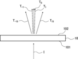
- FIG. 3 is a diagram illustrating a scattering rate calculated by method X.
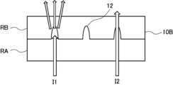
- FIG. FIG. 2 is a diagram illustrating the characteristics of an optical film including region A and region B.
- FIG. 3 is a diagram showing the wavelength dispersion characteristics of the refractive index and absorption coefficient of organic molecules. It is a figure which shows the other aspect of the optical film containing area
- FIG. 3 is a diagram illustrating the characteristics of an optical film including a region C and a region D.
- FIG. 3 is a diagram illustrating the characteristics of an optical film including a region F and a region G.
- 1 is a diagram showing an example of an organic EL display device.
- a numerical range expressed using " ⁇ " means a range that includes the numerical values written before and after " ⁇ " as the lower limit and upper limit.
- the in-plane slow axis and the in-plane fast axis are defined at a wavelength of 550 nm unless otherwise specified. That is, unless otherwise specified, for example, the in-plane slow axis direction means the direction of the in-plane slow axis at a wavelength of 550 nm.
- Re( ⁇ ) and Rth( ⁇ ) represent in-plane retardation and thickness direction retardation at wavelength ⁇ , respectively. Unless otherwise specified, the wavelength ⁇ is 550 nm.
- the average refractive index values of the main optical films are illustrated below: cellulose acylate (1.48), cycloolefin polymer (1.52), polycarbonate (1.59), polymethyl methacrylate (1.49), and polystyrene (1.59).
- visible light intends light with a wavelength of 400 nm or more and less than 700 nm.
- infrared rays refers to light with a wavelength of 700 nm or more
- near infrared refers to light with a wavelength of 700 nm or more and 2000 nm or less
- ultraviolet light refers to light with a wavelength of 10 nm or more and less than 400 nm. do.
- blue light refers to light with a wavelength of 400 to 500 nm
- green light refers to light with a wavelength of more than 500 nm and 600 nm or less
- red light refers to light with a wavelength of more than 600 nm and 700 nm or less.
- “orthogonal” or “parallel” includes the range of error allowed in the technical field to which the present invention belongs. For example, it means that the angle is within a strict angle of ⁇ 5°, and the error from the exact angle is preferably within a range of ⁇ 3°.
- Characteristic points of the optical film of the present invention include that the wavelength ⁇ max determined by method X described later is larger than the wavelength ⁇ min, and the scattering rate max is within a predetermined range.
- Method X which will be described later, when light is incident on an optical film, the wavelength that is most likely to be scattered is calculated for every 10 nm in the wavelength range of 400 to 700 nm.
- the fact that the wavelength ⁇ max is larger than the wavelength ⁇ min means that light that is more easily scattered is located on the long wavelength side.
- an organic EL display element with a micro-cavity structure is viewed from an oblique direction, it is difficult to see light with longer wavelengths (for example, red light) than when viewed from the front. There is. Therefore, if an optical film whose wavelength ⁇ max determined by method Light is more likely to be scattered by the optical film, and as a result, light with longer wavelengths in the oblique direction increases, and the difference in color from the front direction becomes smaller.
- the optical film of the present invention has a wavelength ⁇ max determined by the following method X, which is larger than a wavelength ⁇ min determined by the following method X,
- the scattering rate max determined by method X below is 10 to 90%.
- the integrated value of the transmittance for each 1° in the angle range of -15 to 15° is the integrated value A, and the transmittance for each 1° in the angular range of -1 to 1°.
- the integrated value of is defined as integrated value B, and the ratio of the absolute value of the difference between integrated value A and integrated value B to integrated value A is defined as the scattering rate.
- the largest scattering rate is the scattering rate max
- the wavelength of the incident light that shows the maximum scattering rate is the wavelength ⁇ max
- the wavelength of the incident light that shows the smallest scattering rate Let be the wavelength.
- the method X will be explained in more detail using FIG. 1.
- incident light I is made to enter from the normal direction of one surface 101 of the optical film 10.
- the incident light I light of each wavelength of 10 nm in the wavelength range of 400 to 700 nm is used. More specifically, light of each wavelength (400+10 ⁇ m (m represents an integer from 0 to 30)) (nm) obtained by adding every 10 nm from a wavelength of 400 nm is used as the incident light. That is, the wavelength of the incident light is 400 nm, 410 nm, 420 nm, . . . , 680 nm, 690 nm, 700 nm, each having a wavelength of 10 nm.
- the transmittance of the light transmitted through the optical film 10 is measured every 1° in the angular range of -15° to 15° with respect to the normal direction of the other surface 102 of the optical film 10. That is, the transmittance of transmitted light is measured in each direction of 1° in the angular range of -15° to 15°.
- the transmittance of transmitted light is measured in each direction of 1° in the angular range of -15° to 15°.
- transmitted light T 15 in a direction at an angle of 15° to the normal direction of the surface 102 transmitted light T 1 in a direction at an angle of 1° to the normal direction of the surface 102
- Transmitted light T 0 in the angular direction of 0° with respect to the normal direction of surface 102 Transmitted light T ⁇ 1 in the angular direction of ⁇ 1° with respect to the normal direction of surface 102 , with respect to the normal direction of surface 102
- Transmitted light T -15 in the angular direction of -15° is shown, but the angle at every 1° from -15 to 15° (-15°, -14°, -13°, -12°, -11° , -10°, -9°, -8°, -7°, -6°, -5°, -4°, -3°, -2°, -1°, 0°, 1°, 2°, Measure the transmittance of transmitted light in directions (3°, 4°, 5°, 6°, 7°, 8°, 9°, 10°
- the integrated value A which is the integrated value of the transmittance for each 1° in the angular range of -15° to 15° with respect to the normal direction of the surface 102, obtained above is determined.
- the transmittance of each transmitted light in each 1° angle direction from -15 to 15° with respect to the normal direction of the surface 102 is summed, and the obtained total value (integrated value) is calculated as the integrated value A. shall be.
- the integrated value B which is the integrated value of the transmittance for each 1° in the angle range of -1° to 1° with respect to the normal direction of the surface 102, obtained above is determined.
- the transmittance of the transmitted light T -1 in the direction at an angle of -1° with respect to the normal direction of the surface 102, and the transmittance of the transmitted light T0 in the direction of an angle of 0° with respect to the normal direction of the surface 102 . and the transmittance of the transmitted light T1 in the angular direction of 1° with respect to the normal direction of the surface 102, and the obtained total value (integrated value) is defined as the integrated value B.
- the integrated value B represents the amount of light that is transmitted without being scattered much. Therefore, the greater the absolute value of the difference between the integrated value A and the integrated value B, the greater the degree of scattering of transmitted light. Therefore, the ratio of the absolute value of the difference between the integrated value A and the integrated value B to the integrated value A is defined as the scattering rate.
- the scattering rate at each wavelength which is calculated using light of each wavelength of 10 nm in the wavelength range of 400 to 700 nm as incident light, is calculated by the method described above. For example, light with a wavelength of 600 nm is incident, an integrated value A and an integrated value B are calculated, and the scattering rate at a wavelength of 600 nm is determined. Next, among the obtained scattering rates at each wavelength, the largest scattering rate is set as the scattering rate max, and the wavelength of the incident light showing the scattering rate max is set as the wavelength ⁇ max. On the other hand, among the obtained scattering rates at each wavelength, the wavelength of the incident light showing the smallest scattering rate is defined as the wavelength ⁇ min.
- the wavelength of 650 nm becomes the wavelength ⁇ max.
- the scattering rate obtained when light with a wavelength of 450 nm is used as incident light is larger than the scattering rate of incident light with other wavelengths, the wavelength of 450 nm becomes the wavelength ⁇ min.
- the wavelength ⁇ max determined by the method X described above is larger than the wavelength ⁇ min.
- an optical film that satisfies this characteristic means that light on the longer wavelength side is easily scattered.
- the wavelength ⁇ max is determined by applying the optical film of the present invention to an organic EL display element having a microcavity structure and viewing the obtained organic EL display device from the front direction and from an oblique direction.
- the point where the effect of the present invention is better it is preferably within the range of 580 to 700 nm, and preferably within the range of 600 to 700 nm. More preferably, it is within the range of 610 to 700 nm.
- the wavelength ⁇ min is preferably within the range of 400 to 580 nm, more preferably within the range of 400 to 570 nm, since the effects of the present invention are more excellent.
- the scattering rate max is 10 to 90%.
- the scattering rate max is preferably 40 to 90%, more preferably 55 to 90%, and even more preferably 60 to 90%, since the effects of the present invention are more excellent.
- the above wavelength ⁇ max, wavelength ⁇ min, and scattering rate max can be measured using a commercially available goniophotometer (GCMS-3B).
- the effect of the present invention is more excellent, and the average scattering rate at each wavelength calculated using light of each wavelength of 10 nm in the wavelength range of 580 to 700 nm as incident light.
- the value (hereinafter also simply referred to as "average value 1") is the average value of the scattering rate at each wavelength calculated using light of each wavelength of 10 nm in the wavelength range of 400 to 580 nm as incident light (hereinafter, referred to simply as "average value 1"). It is preferably 1.5 times or more of the average value (also simply referred to as "average value 2"). That is, it is preferable that the ratio of average value 1 to average value 2 is 1.5 or more.
- the ratio of average value 1 to average value 2 is more preferably 1.8 or more, and even more preferably 2.0 or more.
- the upper limit is not particularly limited, but is preferably 8.0 or less, more preferably 5.0 or less.
- the average value 1 is the arithmetic average value of the scattering rates at each wavelength calculated using light of each wavelength of 10 nm in the wavelength range of 580 to 700 nm as incident light.
- the average value 2 is the arithmetic average value of the scattering rates at each wavelength calculated using light of each wavelength of 10 nm in the wavelength range of 400 to 580 nm as incident light.
- the optical film has a region A and a region B having different refractive indexes at any wavelength in the wavelength range of 400 to 700 nm, and
- the refractive index difference between region A and region B is 0.05 or more at each wavelength of 10 nm in the range of 700 nm, and any of the wavelengths of each 10 nm in the wavelength range of 400 to 700 nm.
- an embodiment may be mentioned in which the difference in refractive index between region A and region B is 0.02 or less.
- region A and a region B (RB) that have different refractive indexes at any wavelength within the wavelength range of 400 to 700 nm.
- a sea-island structure is formed in which region B (RB) exists like an island in region A (RA).
- regions A and B are made of different materials, it is possible to achieve a state in which the refractive index is different for a specific wavelength.
- the refractive index difference between region A and region B is 0.05 or more at each wavelength of 10 nm in the wavelength range of 400 to 700 nm.
- the refractive index difference between region A and region B at the wavelength of incident light I1 is 0.05 or more as shown in FIG. Because refraction is likely to occur at the interface, scattering occurs easily.
- the refractive index difference between region A and region B is preferably 0.07 or more, and more preferably 0.10 or more.
- the upper limit is not particularly limited, but is preferably 0.20 or less, more preferably 0.15 or less.
- the difference in refractive index between region A and region B be 0.02 or less at each wavelength of 10 nm in the wavelength range of 400 to 700 nm.
- the difference in refractive index between region A and region B is 0.02 or less at each wavelength of 10 nm in the wavelength range of 400 to 700 nm.
- the refractive index difference between region A and region B at the wavelength of incident light I2 is 0.02 or less as shown in FIG. Because refraction is less likely to occur at the interface, it can pass through without being scattered.
- the refractive index difference between region A and region B is 0.02 or less
- the refractive index difference between region A and region B is preferably 0.015 or less, more preferably 0.01 or less.
- the lower limit is not particularly limited, but may be 0.
- the difference in refractive index of that wavelength (region The wavelength where the refractive index difference between region A and region B can be 0.05 or more) easily corresponds to the above-mentioned wavelength ⁇ max.
- the wavelength (the wavelength at which the refractive index difference between region A and region B can be 0.02 or less) easily corresponds to the above-mentioned wavelength ⁇ min.
- the optical film has the above-mentioned preferred embodiment, it is possible to cause the scattering of the light with the wavelength ⁇ max as described above, and prevent the scattering of the light with the wavelength ⁇ min.
- the wavelength at which the difference in refractive index between region A and region B is maximum is selected among each wavelength of 10 nm in the wavelength range of 400 to 700 nm.
- ⁇ 1 is the wavelength at which the difference in refractive index between the region A and the region B is minimum is the wavelength ⁇ 2
- the wavelength ⁇ 1 is longer than the wavelength ⁇ 2.
- wavelength ⁇ 1 tends to correspond to the above-mentioned wavelength ⁇ max
- wavelength ⁇ 2 corresponds to the above-mentioned wavelength ⁇ min.
- the preferred range of the wavelength ⁇ 1 is the same as the preferred range of the wavelength ⁇ max described above.
- the preferred range of the wavelength ⁇ 2 is the same as the preferred range of the wavelength ⁇ min described above.
- the refractive index difference between region A and region B is 0.05 or more at any wavelength in 10 nm increments in the wavelength range of 580 to 700 nm, and that the refractive index difference between region A and region B is 0.02 or less at any wavelength in 10 nm increments in the wavelength range of 400 to 580 nm.
- the refractive index difference between region A and region B is 0.05 or more at any wavelength in 10 nm increments in the wavelength range of 600 to 650 nm, and that the refractive index difference between region A and region B is 0.02 or less at any wavelength in 10 nm increments in the wavelength range of 400 to 570 nm.
- the refractive index wavelength dispersion characteristics of general organic molecules will be explained with reference to FIG.
- the upper side shows the behavior of the refractive index with respect to wavelength
- the lower side shows the behavior of absorption characteristics (absorption spectrum) with respect to wavelength.
- the refractive index n of organic molecules in a region away from the characteristic absorption wavelength (region a in FIG. 3) monotonically decreases as the wavelength increases. This kind of dispersion is called “normal dispersion.”
- the refractive index n in the wavelength range including intrinsic absorption region b in FIG. 3 rapidly increases as the wavelength increases.
- Such dispersion is called "abnormal dispersion.” That is, as shown in FIG. 3, an increase or decrease in the refractive index is observed immediately before the wavelength region where absorption occurs.
- an infrared absorbing dye is contained in region A (RA) of the optical film 10A shown in FIG. More specifically, when an infrared absorbing dye having a maximum absorption wavelength of 700 nm or more (preferably about 700 to 1200 nm) is included in region A (RA), as shown in FIG. Under the influence of the characteristic of "normal dispersion" in which the refractive index rapidly decreases in the visible light region, for example, the refractive index in region A in the long wavelength range (for example, the wavelength range of 580 to 700 nm) is , is smaller than the refractive index in other wavelength ranges.
- the refractive index in the long wavelength range (for example, the wavelength range of 580 to 700 nm) can be made smaller than the refractive index in the short wavelength range (for example, the wavelength range of 400 to 580 nm).
- Such an optical film can easily achieve the above-described relationship between the wavelength ⁇ max and the wavelength ⁇ min, and the relationship between the wavelength ⁇ 1 and the wavelength ⁇ 2.
- region A contains the above-mentioned predetermined near-infrared absorbing dye
- the difference between region A and region B at each wavelength in the short wavelength range for example, a wavelength range of 400 to 580 nm
- the refractive index difference remains small
- the refractive index difference between region A and region B increases at each wavelength in the long wavelength range (for example, a wavelength range of 580 to 700 nm), so that the above-mentioned predetermined characteristics are satisfied. Easy to obtain optical film.
- the near-infrared absorbing dye is contained in the region A that exists in the form of a sea, but the near-infrared absorbing dye may also be contained in the region B that exists in the form of an island.
- near-infrared absorbing dyes dyes exhibiting other absorption characteristics may also be used.
- a visible light absorbing dye that exhibits a maximum absorption wavelength at a wavelength of 500 nm is used in place of the near-infrared absorbing dye described above for region A existing in the shape of a sea, in a region shorter than the wavelength of 500 nm (for example, 450 nm ⁇ 20 nm)
- the refractive index decreases in the wavelength region), and the refractive index increases in the wavelength region longer than 500 nm (for example, in the range of 550 nm ⁇ 20 nm).
- the dye to be used can be appropriately selected depending on which wavelength of light is desired to be scattered.
- FIG. 4 is a cross-sectional view of another embodiment of an optical film in which the distribution states of region A and region B are different.
- the optical film 10B has a layered region A (RA) and a layered region B (RB), and the region A has a convex portion 12 protruding toward the region B side.
- the optical film has a region C and a region D having different refractive indexes at any wavelength in the wavelength range of 400 to 700 nm, and the region C has a region C and a region D having different refractive indexes.
- Examples include an embodiment in which a polymer is included and region D is composed of a pigment.
- the characteristics of the optical film that satisfies the above configuration will be explained using FIG. 5.
- the optical film 10C shown in FIG. 5 has a region C (RC) and a region D (RD) that have different refractive indexes at any wavelength within the wavelength range of 400 to 700 nm.
- RC region C
- RD region D
- region D exists like an island in region C (RC).
- regions C and D are made of different materials, it is possible to achieve a state in which the refractive index is different for a specific wavelength.
- the refractive index difference between region C and region D is 0.05 or more at any of the wavelengths in 10 nm intervals in the wavelength range of 400 to 700 nm.
- the incident light is likely to be scattered in the optical film. More specifically, when the refractive index difference between region C and region D at the wavelength of incident light I1 shown in Figure 5 is 0.05 or more, the incident light I1 is likely to be refraction or the like at the interface between region C and region D, and is therefore likely to be scattered.
- the refractive index difference between the region C and the region D is 0.05 or more
- the refractive index difference between the region C and the region D is preferably 0.07 or more, more preferably 0.10 or more.
- the refractive index difference is preferably 1.5 or less, more preferably 1.0 or less.
- the difference in refractive index between region C and region D be 0.02 or less at each wavelength of 10 nm in the wavelength range of 400 to 700 nm.
- the difference in refractive index between region C and region D is 0.02 or less at each wavelength of 10 nm in the wavelength range of 400 to 700 nm.
- the refractive index difference between the region C and the region D is 0.02 or less
- the refractive index difference between the region C and the region D is preferably 0.015 or less, more preferably 0.01 or less.
- the lower limit is not particularly limited, but may be 0.
- the difference in the refractive index of that wavelength (region The wavelength where the difference in refractive index between C and region D is 0.05 or more) easily corresponds to the above-mentioned wavelength ⁇ max.
- the wavelength (the wavelength at which the refractive index difference between the region C and the region D can be 0.02 or less) easily corresponds to the above-mentioned wavelength ⁇ min.
- the optical film has the above-mentioned preferred embodiment, it is possible to cause the scattering of the light with the wavelength ⁇ max as described above, and prevent the scattering of the light with the wavelength ⁇ min.
- the wavelength at which the difference in refractive index between the region C and the region D is the maximum is selected from among each wavelength of 10 nm in the wavelength range of 400 to 700 nm.
- ⁇ 1 is the wavelength at which the difference in refractive index between the region C and the region D is minimum is the wavelength ⁇ 2
- the wavelength ⁇ 1 is longer than the wavelength ⁇ 2.
- wavelength ⁇ 1 tends to correspond to the above-mentioned wavelength ⁇ max
- wavelength ⁇ 2 corresponds to the above-mentioned wavelength ⁇ min.
- the preferred range of the wavelength ⁇ 1 is the same as the preferred range of the wavelength ⁇ max described above.
- the preferred range of the wavelength ⁇ 2 is the same as the preferred range of the wavelength ⁇ min described above.
- the effect of the present invention is more excellent, and the difference in refractive index between region C and region D is 0.05 or more at each wavelength of 10 nm in the wavelength range of 580 to 700 nm.
- the difference in refractive index between region C and region D be 0.02 or less at each wavelength of 10 nm in the wavelength range of 400 to 580 nm.
- the refractive index difference between region C and region D be 0.05 or more at each wavelength of 10 nm in the wavelength range of 600 to 650 nm, and It is preferable that the difference in refractive index between region C and region D be 0.02 or less at any one of the wavelengths.
- the region D (RD) of the optical film 10C shown in FIG. 5 is made of a pigment. More specifically, when region D (RD) is composed of a pigment having a maximum absorption wavelength of 700 nm or more (preferably about 700 to 1200 nm), as shown in FIG. Under the influence of the characteristic of "normal dispersion" in which the refractive index rapidly decreases in the visible light region, for example, the refractive index in region D in the long wavelength range (for example, the wavelength range of 580 to 700 nm) is The refractive index is smaller than the refractive index in other wavelength ranges.
- the refractive index in the long wavelength range (for example, the wavelength range of 580 to 700 nm) can be made smaller than the refractive index in the short wavelength range (for example, the wavelength range of 400 to 580 nm).
- Such an optical film can easily achieve the above-described relationship between the wavelength ⁇ max and the wavelength ⁇ min, and the relationship between the wavelength ⁇ 1 and the wavelength ⁇ 2.
- region D is composed of a pigment having the above-mentioned predetermined maximum absorption wavelength
- region C and region at each wavelength in a short wavelength range (for example, a wavelength range of 400 to 580 nm)
- the refractive index difference between region C and region D remains small
- the refractive index difference between region C and region D increases at each wavelength in the long wavelength range (for example, a wavelength range of 580 to 700 nm). It is easy to obtain an optical film that satisfies the characteristics.
- the scattering rate max is preferably 10 to 50%, more preferably 15 to 50%, and even more preferably 20 to 50%. , 20 to 40% is particularly preferred.
- the optical film having the above-mentioned regions C and D may further include a region E which is a region having a different refractive index from both of the regions C and D.
- Region E is preferably composed of particles having an average particle diameter of 4.0 to 9.0 ⁇ m.
- the refractive index difference between the region E and the region C is not particularly limited, but the refractive index difference between the region E and the region C is 0.1 or more at each wavelength of 10 nm in the wavelength range of 400 to 700 nm. It is preferably 0.12 or more, and more preferably 0.12 or more.
- the optical film has a region F and a region G having different refractive indexes at any wavelength in the wavelength range of 400 to 700 nm
- examples include an embodiment in which a polymer is included and region G is composed of particles having an average particle diameter of 4.0 to 9.0 ⁇ m.
- the characteristics of the optical film that satisfies the above configuration will be explained using FIG. 6.
- the optical film 10D shown in FIG. 6 has a region F (RF) and a region G (RG) that have different refractive indexes at any wavelength within the wavelength range of 400 to 700 nm.
- a sea-island structure is formed in which region F (RF) exists like an island in region G (RG).
- the refractive index difference between region F and region G is preferably 0.10 or more, more preferably 0.12 or more at any wavelength from 400 to 700 nm.
- the upper limit of the refractive index difference is not particularly limited, but is preferably 0.20 or less.
- the refractive index difference between region F and region G is preferably 0.08 or more, more preferably 0.10 or more at any wavelength from 400 to 700 nm.
- the upper limit of the refractive index difference is not particularly limited, but is preferably 0.20 or less.
- the region G since the region G is composed of particles of a predetermined size, it exhibits the above-mentioned characteristics. That is, by using particles having an average particle diameter of 4.0 to 9.0 ⁇ m, light having wavelengths in the long wavelength range (for example, wavelengths in the range of 580 to 700 nm) is easily scattered.
- the thickness of the optical film is not particularly limited, but from the viewpoint of thinning, it is preferably 40 ⁇ m or less, more preferably 20 ⁇ m or less.
- the lower limit is not particularly limited, but is preferably 1 ⁇ m or more.
- the material used for the optical film is not particularly limited as long as it exhibits the above-mentioned characteristics.
- the optical film contains a polymer.
- the type of polymer is not particularly limited, but examples include poly(meth)acrylate, polyester, polystyrene, polycarbonate, polyolefin, and polyurethane. Note that, as described later, when an optical film is formed using a polymerizable composition containing a monomer, the cured product of the monomer may correspond to the above-mentioned polymer.
- region A contains a dye and a polymer
- region B is composed of particles (preferably organic particles). Note that, as shown in FIG. 2, region A and region B preferably form a sea-island structure in which region A is arranged like a sea and region B is arranged like an island.
- the type of polymer contained in region A is not particularly limited, and examples include the materials listed as examples of polymers that may be contained in the optical film described above. Further, the polymer contained in region A may be an adhesive.
- the content of the polymer contained in region A is not particularly limited, but is preferably 50 to 99% by weight, more preferably 60 to 90% by weight, based on the total weight of the optical film.
- an optimal dye is selected depending on the wavelength of light to be scattered.
- infrared absorbing dyes are preferred.
- An infrared absorbing dye is a dye that has a maximum absorption wavelength in the infrared region.
- the molecular weight of the infrared absorbing dye is not particularly limited, but is preferably less than 5000.
- the lower limit is not particularly limited, but is often 500 or more.
- infrared absorbing dyes examples include diketopyrrolopyrrole dyes, diimmonium dyes, phthalocyanine dyes, naphthalocyanine dyes, azo dyes, polymethine dyes, anthraquinone dyes, pyrylium dyes, squarylium dyes, and triphenyl.
- examples include methane dyes, cyanine dyes, aminium dyes, croconium dyes, rylene dyes, metal complex dyes, oxonol dyes, merocyanine dyes, and dithienophosphorine dyes.
- One type of infrared absorbing dye may be used alone, or two or more types may be used in combination.
- the infrared absorbing dye a dye having a maximum absorption wavelength in the near infrared region (near infrared absorbing dye) is preferable.
- the maximum absorption wavelength of the infrared absorbing dye is preferably located in a wavelength range of 700 nm or more, more preferably located in a wavelength range of 700 to 1200 nm, and more preferably located in a wavelength range of 700 to 900 nm, since the effect of the present invention is more excellent.
- the absorption spectrum of the dye is measured to determine the maximum absorption wavelength of the dye.
- the content of the dye contained in Region A is not particularly limited, but is preferably 0.5 to 50% by mass, more preferably 2 to 30% by mass, based on the total mass of the polymer contained in Region A.
- the particles constituting region B may be either organic particles or inorganic particles, and are preferably organic particles. Moreover, it is preferable that the organic particles contain a polymer. Examples of the type of polymer include the materials exemplified as polymers that may be included in the optical film described above.
- the material constituting the inorganic particles is not particularly limited, and examples include nonmetal oxides (eg, silicon dioxide), metal oxides (eg, aluminum oxide), and metal nitrides. Note that the polymer contained in region A and the polymer contained in the organic particles constituting region B may be the same or different in type.
- the average particle diameter of the particles is not particularly limited, it is preferably 5.0 ⁇ m or less, more preferably 2.0 ⁇ m or less, since the effects of the present invention are more excellent.
- the lower limit is not particularly limited, but is preferably 0.1 ⁇ m or more, more preferably 0.5 ⁇ m or more.
- the content of particles contained in region B is not particularly limited, but is preferably 5 to 40% by mass, more preferably 10 to 30% by mass, based on the total mass of the optical film.
- region C contains a polymer and the region D is composed of a pigment, as described above.
- region C and region D preferably form a sea-island structure in which region C is arranged like a sea and region D is arranged like an island.
- the type of polymer contained in region C is not particularly limited, and examples thereof include the materials listed as examples of polymers that may be contained in the optical film described above.
- the content of the polymer contained in region C is not particularly limited, but is preferably 50 to 95% by mass, more preferably 60 to 90% by mass, based on the total mass of the optical film.
- the type of pigment constituting region D is not particularly limited, and as described above, the optimal pigment is selected depending on the wavelength of the light to be scattered. Among these, pigments having a maximum absorption wavelength of 700 nm or more are preferred. The maximum absorption wavelength of the pigment is preferably located in the range of 700 to 1200 nm, more preferably in the range of 700 to 1000 nm.
- a polystyrene film containing a pigment pigment concentration in the film: 20% by mass
- a polystyrene film that does not contain a pigment as a reference and measure it with a spectrophotometer ( Using UV-3150 (manufactured by Shimadzu Corporation), the absorption spectrum of the pigment is measured by comparing the two, and the maximum absorption wavelength of the pigment is determined.
- the type of pigment is not particularly limited, but examples include cyanine compounds, phthalocyanine compounds, quinone compounds, squarylium compounds, croconium compounds, azo compounds, diimmonium compounds, perylene compounds, and pyrrolopyrrole compounds.
- One type of pigment may be used alone, or two or more types may be used in combination.
- the average particle diameter of the pigment is not particularly limited, but from the viewpoint of achieving better effects of the present invention, it is preferably from 0.3 to 5.0 ⁇ m, more preferably from 0.3 to 2.0 ⁇ m.
- the cross section of the optical film is observed with a scanning electron microscope, the major axis of the observed pigment is measured at at least 10 points, and the value obtained by arithmetic averaging of the measurements is, The average particle diameter of the pigment.
- the amount of pigment that constitutes region D is not particularly limited, but is preferably 5 to 50% by mass, and more preferably 10 to 40% by mass, relative to the total mass of the optical film.
- the optical film may have a region E which is a region having a different refractive index from both region C and region D.
- Region E is preferably composed of particles having an average particle diameter of 4.0 to 9.0 ⁇ m.
- the average particle diameter of the particles is preferably 4.5 to 8.5 ⁇ m.
- the above particles may be organic particles or inorganic particles. Among these, organic particles are preferred, and polymer particles are more preferred.
- the type of polymer contained in the polymer particles is not particularly limited, and examples thereof include the materials listed as examples of polymers that may be contained in the optical film described above.
- the content of particles contained in region E is not particularly limited, but is preferably 5 to 40% by mass, more preferably 10 to 30% by mass, based on the total mass of the optical film.
- region F contains a polymer, and region F is composed of particles having an average particle diameter of 4.0 to 9.0 ⁇ m. preferable.
- region F and region G preferably form a sea-island structure in which region F is arranged like a sea and region G is arranged like an island.
- the type of polymer contained in region F is not particularly limited, and examples thereof include the materials listed as examples of polymers that may be contained in the optical film described above.
- the content of the polymer contained in region F is not particularly limited, but is preferably 50 to 95% by mass, more preferably 60 to 90% by mass, based on the total mass of the optical film.
- Examples of particles constituting region G include particles constituting region E described above and having an average particle diameter of 4.0 to 9.0 ⁇ m.
- the content of particles contained in region E is not particularly limited, but is preferably 5 to 40% by mass, more preferably 10 to 30% by mass, based on the total mass of the optical film.
- the method for producing the optical film is not particularly limited, and any known method can be used. Among these methods, a method using a polymerizable composition is mentioned because it is easy to manufacture an optical film.
- Components contained in the polymerizable composition include, for example, monomers, dyes, and particles.
- the monomer used is not particularly limited as long as it is a monomer that can constitute the polymer contained in the above-mentioned region A after polymerization.
- examples of the dyes used include those contained in the region A described above.
- the particles used the particles forming the region B mentioned above can be mentioned.
- the polymerizable composition may contain other components than those mentioned above.
- Other components include a polymerization initiator.
- the polymerization initiator used is selected depending on the type of polymerization reaction, and includes, for example, a thermal polymerization initiator and a photopolymerization initiator.
- other components include a leveling agent, a plasticizer, and a solvent.
- Examples of the procedure for producing an optical film using a polymerizable composition include a method in which the polymerizable composition is applied onto a substrate and the resulting coating film is subjected to a curing treatment.
- the type of base material used is not particularly limited, and includes known base materials.
- the base material may be a so-called temporary support. That is, when the base material is a temporary support, an optical film with a temporary support containing the temporary support and the optical film is finally obtained. Since the temporary support is removable, the optical film with the temporary support can be used as a so-called transfer film.
- Methods for applying the polymerizable composition include curtain coating method, dip coating method, spin coating method, print coating method, spray coating method, slot coating method, roll coating method, slide coating method, blade coating method, gravure coating method, and wire bar method.
- the method of curing treatment is not particularly limited, and examples include light irradiation treatment and heat treatment. Among these, from the viewpoint of manufacturing suitability, light irradiation treatment is preferred, and ultraviolet irradiation treatment is more preferred.
- the irradiation conditions for the light irradiation treatment are not particularly limited, but an irradiation amount of 50 to 1000 mJ/cm 2 is preferable.
- an optical film when manufacturing an optical film including region C and region D, a method for manufacturing the optical film using a composition containing a polymer and a pigment can be mentioned. More specifically, an optical film can be manufactured by applying a composition containing a polymer, a pigment, and a solvent and subjecting the formed coating film to a drying treatment (eg, heat treatment).
- a drying treatment eg, heat treatment
- the preparation of the composition includes a process of dispersing the pigment.
- mechanical forces used to disperse pigments include compression, squeezing, impact, shearing, cavitation, and the like.
- the optical film of the present invention described above is suitably applied to an organic EL display element.
- the organic EL display device of the present invention preferably includes an organic EL display element having a microcavity structure and the optical film of the present invention described above.
- FIG. 7 shows an example of an organic EL display device of the present invention.
- the organic EL display device 20 shown in FIG. 7 includes an organic EL display element 22, an optical film 10, and a circularly polarizing plate 24.
- the circularly polarizing plate 24 includes an optically anisotropic layer 26 and a polarizer 28.
- the circularly polarizing plate 24 is an arbitrary member.
- the optical film 10 is as described above, and a description thereof will be omitted.
- the organic EL display element has a microcavity structure.
- a microcavity structure is a structure that resonates only light of a predetermined wavelength and weakens light of other wavelengths by matching the optical path length to the peak wavelength of the spectrum of the light to be extracted. More specifically, by matching the optical path length between the upper and lower electrodes of the organic EL display element to each peak wavelength of red light, green light, blue light, etc. emitted from the organic EL display element, the distance between the electrodes can be adjusted. This is a structure in which light is repeatedly reflected at the center, causing only the light at the peak wavelength to resonate and be emphasized, while attenuating light outside the peak wavelength (microcavity effect).
- the microcavity structure may be any structure as long as it can provide the above effects, and any known structure may be employed.
- the organic EL display element is preferably a display element that emits at least blue light, green light, and red light. That is, the organic EL display element preferably has a blue light emitting section, a green light emitting section, and a red light emitting section.
- the organic EL display element may be a top emission type organic EL display element or a bottom emission type organic EL display element.
- a circularly polarizing plate is an optical element that converts unpolarized light into circularly polarized light.
- the circularly polarizing plate is placed on the organic EL display element and contributes to preventing reflection of external light. It is preferable that the circularly polarizing plate is placed closer to the viewing side than the optical film.
- a circularly polarizing plate includes an optically anisotropic layer and a polarizer.
- the optically anisotropic layer includes a ⁇ /4 plate.
- a ⁇ /4 plate is a plate that has a ⁇ /4 function, and specifically, a plate that has the function of converting linearly polarized light of a certain wavelength into circularly polarized light (or from circularly polarized light to linearly polarized light).
- Specific examples of the ⁇ /4 plate include, for example, the ⁇ /4 plate described in US Patent Application Publication No. 2015/0277006.
- examples of embodiments in which the ⁇ /4 plate has a single layer structure include a stretched polymer film and an optically anisotropic layer formed using a liquid crystal compound.
- a specific example is a broadband ⁇ /4 plate formed by laminating a ⁇ /4 plate and a ⁇ /2 plate.
- the Re(550) of the ⁇ /4 plate is not particularly limited, but is preferably 110 to 160 nm, more preferably 120 to 150 nm, since it is useful as a ⁇ /4 plate.
- the ⁇ /4 plate preferably exhibits reverse wavelength dispersion.
- a ⁇ /4 plate exhibiting reverse wavelength dispersion means that when measuring the in-plane retardation (Re) value at a specific wavelength (visible light range), the Re value becomes equal or higher as the measurement wavelength becomes larger. means.
- the optically anisotropic layer may include layers other than the ⁇ /4 plate. Examples of other layers include a C plate.
- the polarizer may be any member (linear polarizer) that has the function of converting light into a specific linearly polarized light, and an absorptive polarizer can be mainly used.
- the absorption type polarizer include an iodine-based polarizer, a dichroic material-based polarizer using a dichroic material, and a polyene-based polarizer.
- the iodine-based polarizer and the dichroic material-based polarizer include a coating type polarizer and a stretching type polarizer, and any of them can be used, but a polarizer produced by adsorbing iodine or a dichroic material to polyvinyl alcohol and stretching it is preferable.
- the relationship between the absorption axis of the polarizer and the in-plane slow axis of the ⁇ /4 plate is not particularly limited, but from the viewpoint of enabling a laminate of a polarizer and a ⁇ /4 plate to function suitably as a circular polarizing plate, the angle between the absorption axis of the polarizer and the in-plane slow axis of the ⁇ /4 plate is preferably 45° ⁇ 10°.
- the organic EL display device may include members other than those described above.
- Other members include an adhesive layer.
- the adhesive layer By arranging the adhesive layer between each member, the adhesion between each member can be improved.
- the adhesive layer may be placed between the organic EL display element and the optical film.
- the adhesive layer may be arranged between the optical film and the circularly polarizing plate.
- the adhesive layer may be arranged between the optically anisotropic layer and the polarizer in the circularly polarizing plate.
- the material constituting the adhesive layer is not particularly limited, and includes known materials.
- the average refractive index of the adhesive layer at a wavelength of 400 to 700 nm is not particularly limited, but is preferably 1.5 to 1.6.
- the other members include a color filter.
- the color filters preferably include a blue color filter, a green color filter, and a red color filter.
- the color filter may also have a black matrix.
- Example 1 (Preparation of optical laminate) A polymerizable liquid crystal composition A having the following composition was prepared.
- Mixture A of rod-shaped liquid crystal compounds (hereinafter referred to as mixture of compounds)
- A-400 (Shin Nakamura Chemical Industry Co., Ltd.)
- Polymer A (The numerical value in the formula below indicates the content (mass%) of each repeating unit with respect to all repeating units in the polymer. The weight average molecular weight was 58,000.)
- the weight average molecular weight was 70,000. Ta.
- the prepared polymerizable liquid crystal composition A was applied onto a cellulose polymer film (TG40, manufactured by Fujifilm) as a base material using a #3.0 wire bar, heated at 70°C for 2 minutes, and the oxygen concentration was adjusted.
- Ultraviolet rays of 150 mJ/cm 2 were irradiated under the condition that the amount of UV rays was less than 100 volume ppm.
- optically anisotropic layer A having a thickness of 0.7 ⁇ m.
- the optically anisotropic layer A was a positive C plate.
- the retardation Rth (550) of the optically anisotropic layer A in the thickness direction was ⁇ 70 nm.
- a polymerizable liquid crystal composition B having the following composition was prepared.
- Leveling agent A (The numbers in the formula below indicate the content (mass%) of each repeating unit relative to the total repeating units in the polymer. The weight average molecular weight was 12,500.)
- Polymerizable liquid crystal composition B was applied onto the previously formed optically anisotropic layer A using a wire bar coater #7 to form a composition layer.
- the formed composition layer was once heated to 120°C on a hot plate, and then cooled to 60°C to stabilize the orientation. After that, the film temperature was kept at 60°C under a nitrogen atmosphere (oxygen concentration less than 100 volume ppm) using an ultra-high pressure mercury lamp, and after the first ultraviolet irradiation (80 mJ/cm 2 ), the film temperature was kept at 100°C.
- the orientation was fixed by a second ultraviolet irradiation (300 mJ/cm 2 ), an optically anisotropic layer B having a thickness of 2.8 ⁇ m was formed, and an optical laminate was produced.
- the optically anisotropic layer B was a positive A plate.
- the in-plane retardation Re (550) at a wavelength of 550 nm was 141 nm, and the angle of the in-plane slow axis with respect to the film width direction was 45°.
- the above angle is determined counterclockwise when the optically anisotropic layer B disposed on the optically anisotropic layer A is observed from the optically anisotropic layer B side, with the width direction of the film as a reference (0°). It is an angle expressed as a positive value.
- the optical laminate prepared above was placed on the TAC film side of the prepared polarizer with a protective film via the adhesive layer B described in Example 4 of JP-A-2021-015294, so that the optically anisotropic layer B side
- the protective film-attached polarizer was attached to the TAC film side, and the angle between the absorption axis of the polarizer and the in-plane slow axis of the optically anisotropic layer B was 45°.
- the cellulose-based polymer film serving as a base material was peeled off from the optically anisotropic layer A to produce a circularly polarizing plate.
- Leveling agent B (The numerical value in the formula below indicates the content (mass%) of each repeating unit with respect to all repeating units in the polymer. The weight average molecular weight was 12,500.)
- Ph represents a phenyl group.
- the prepared polymerizable composition A was applied onto a cellulose-based polymer film (Z-TAC, manufactured by Fujifilm) as a base material using a #16 wire bar, heated at 60°C for 1 minute, and the oxygen concentration was adjusted.
- An optical film A having a thickness of 12 ⁇ m was formed on the substrate by irradiating ultraviolet light at 150 mJ/cm 2 under conditions of less than 100 volume ppm. Note that the average particle diameter of the particles derived from Techpolymer SSX-102 contained in optical film A was 2 ⁇ m.
- Optical film A corresponds to an optical film having region A and region B described above.
- Example 2 An organic EL display device was produced in the same manner as in Example 1, except that optical film A was changed to optical film B produced by the method described below.
- the prepared polymerizable composition B was applied onto a cellulose polymer film (Z-TAC, manufactured by Fujifilm) as a base material using a #16 wire bar, heated at 60°C for 1 minute, and the oxygen concentration was adjusted.
- An optical film B having a thickness of 12 ⁇ m was formed on the substrate by irradiating ultraviolet light at 150 mJ/cm 2 under conditions of less than 100 volume ppm. Note that the average particle diameter of the particles derived from Techpolymer SSX-110 contained in optical film B was 10 ⁇ m.
- Optical film B corresponds to the optical film having region A and region B described above.
- Example 3 An organic EL display device was produced in the same manner as in Example 1, except that optical film A was changed to optical film C produced by the following method.
- composition C having the following composition was prepared.
- composition C ⁇ ⁇ Polymethyl methacrylate (Mw: 120,000 manufactured by Sigma-Aldrich) 100 parts by mass ⁇ Dye A above 0.5 parts by mass ⁇ Techpolymer SSX-102 (manufactured by Sekisui Plastics Co., Ltd.) 5 parts by mass ⁇ Tetrahydrofuran 598 Mass part ⁇
- the prepared composition C was applied to a cellulose-based polymer film (Z-TAC, manufactured by Fujifilm Corporation) as a substrate using a #40 wire bar and heated at 60° C. for 1 minute to form an optical film C having a thickness of 10 ⁇ m on the substrate.
- the average particle size of the particles derived from Techpolymer SSX-102 contained in the optical film C was 2 ⁇ m.
- the optical film C corresponds to the optical film having the region A and the region B described above.
- Example 4 An organic EL display device was produced in the same manner as in Example 1, except that optical film A was changed to optical film D produced by the method described below.
- composition D having the following composition was prepared.
- composition D ⁇ ⁇ Polybenzyl methacrylate (average Mw: ⁇ 100,000 manufactured by Sigma-Aldrich) 80 parts by mass ⁇ Pigment B below 20 parts by mass ⁇ Propylene glycol monomethyl ether acetate 525 parts by mass ⁇ ⁇
- Pigment B Ph represents a phenyl group.
- the following dispersion of Pigment B was prepared in advance, and the obtained dispersion and each component were mixed to prepare the above-mentioned Composition D.
- the method for preparing the dispersion of pigment B is as follows. First, a liquid mixture consisting of pigment B (20 parts by mass) and propylene glycol monomethyl ether acetate (80 parts by mass) was mixed using an Ultra Apex mill manufactured by Kotobuki Kogyo Co., Ltd. as a circulating dispersion device (bead mill). A dispersion treatment of pigment B was performed under the following conditions to produce a dispersion liquid of pigment B. Note that the dispersion treatment was carried out until the pigment reached a predetermined size.
- Bead diameter 0.2mm in diameter
- Bead filling rate 65% by volume
- Circumferential speed 6m/sec
- Cooling water Tap water Bead mill Annular passage volume: 0.15L
- Amount of mixed liquid to be dispersed 0.65kg
- the prepared composition D was applied onto a cellulose-based polymer film (Z-TAC, manufactured by Fujifilm) as a base material using a #18 wire bar, heated at 60°C for 1 minute, and a thick layer was applied onto the base material.
- An optical film D having a thickness of 6 ⁇ m was formed.
- the average particle diameter of pigment B contained in optical film D was 1.5 ⁇ m.
- Optical film D corresponds to an optical film having region C and region D described above.
- Example 5 An organic EL display device was produced in the same manner as in Example 1, except that optical film A was changed to optical film E produced by the method described below.
- composition E having the following composition was prepared.
- composition E ⁇ ⁇ Polybenzyl methacrylate (average Mw: ⁇ 100,000 manufactured by Sigma-Aldrich) 80 parts by mass ⁇ Pigment C below 20 parts by mass ⁇ Propylene glycol monomethyl ether acetate 525 parts by mass ⁇ ⁇
- Pigment C. Ph represents a phenyl group.
- a dispersion liquid of Pigment C was prepared in advance, and the obtained dispersion liquid and each component were mixed to prepare the above-mentioned Composition E.
- the dispersion of pigment C was the same as that of pigment B in Example 4 described above, except that pigment C was used instead of pigment B, and the dispersion treatment time was adjusted so that the size of the pigment was a predetermined size. It was prepared according to the same procedure as the dispersion.
- the prepared composition E was applied onto a cellulose-based polymer film (Z-TAC, manufactured by Fujifilm) as a base material using a #18 wire bar, heated at 60°C for 1 minute, and a thick layer was applied onto the base material.
- An optical film E having a thickness of 6 ⁇ m was formed.
- the average particle diameter of the pigment C contained in the optical film E was 1.5 ⁇ m.
- Optical film E corresponds to an optical film having region C and region D described above.
- Example 6 An organic EL display device was produced in the same manner as in Example 1, except that optical film A was changed to optical film F produced by the method described below.
- composition F having the following composition was prepared.
- composition F ⁇ ⁇ Polybenzyl methacrylate (average Mw: ⁇ 100,000 manufactured by Sigma-Aldrich) 80 parts by mass ⁇ Pigment D below 20 parts by mass ⁇ Propylene glycol monomethyl ether acetate 525 parts by mass ⁇ ⁇
- Pigment D Ph represents a phenyl group.
- a dispersion of Pigment D was prepared in advance, and the obtained dispersion and each component were mixed to prepare the above-mentioned Composition F.
- the dispersion of Pigment D was the same as Pigment B in Example 4, except that Pigment D was used instead of Pigment B, and the dispersion treatment time was adjusted so that the size of the pigment was a predetermined size. It was prepared according to the same procedure as the dispersion.
- the prepared composition F was applied onto a cellulose-based polymer film (Z-TAC, manufactured by Fujifilm) as a base material using a #18 wire bar, heated at 60°C for 1 minute, and a thick layer was applied onto the base material.
- An optical film F having a thickness of 6 ⁇ m was formed.
- the average particle diameter of the pigment D contained in the optical film F was 1.5 ⁇ m.
- Optical film F corresponds to an optical film having region C and region D described above.
- Example 7 An organic EL display device was produced in the same manner as in Example 1, except that optical film A was changed to optical film G produced by the method described below.
- composition G having the following composition was prepared.
- composition G ⁇ ⁇ Polybenzyl methacrylate (average Mw: ⁇ 100,000 manufactured by Sigma-Aldrich) 80 parts by mass ⁇ Pigment B above 10 parts by mass ⁇ Techpolymer SSX-105 (manufactured by Sekisui Plastics Co., Ltd.) 10 parts by mass ⁇ Propylene glycol monomethyl Ether acetate 525 parts by mass ⁇
- a dispersion liquid of Pigment B was prepared in advance, and the obtained dispersion liquid and each component were mixed to prepare the above-mentioned Composition G.
- the dispersion of pigment B was prepared according to the same procedure as the dispersion of pigment B in Example 4, except that the dispersion treatment time was adjusted so that the size of the pigment was a predetermined size. did.
- the prepared composition G was applied onto a cellulose-based polymer film (Z-TAC, manufactured by Fujifilm) as a base material using a #26 wire bar, heated at 60°C for 1 minute, and a thick layer was applied onto the base material.
- An optical film G having a thickness of 8 ⁇ m was formed.
- the average particle size of pigment B contained in optical film G was 1.5 ⁇ m, and the average particle size of particles derived from Techpolymer SSX-105 was 6 ⁇ m.
- the optical film G corresponds to an optical film having the region C and the region D described above.
- Example 8 An organic EL display device was produced in the same manner as in Example 1, except that optical film A was changed to optical film H produced by the method described below.
- composition H having the following composition was prepared.
- composition H when preparing Composition H, the above-mentioned Composition H was prepared by preparing a dispersion liquid of Pigment C in advance, and mixing the obtained dispersion liquid and each component.
- the dispersion of pigment C was the same as that of pigment B in Example 4 described above, except that pigment C was used instead of pigment B, and the dispersion treatment time was adjusted so that the size of the pigment was a predetermined size. It was prepared according to the same procedure as the dispersion.
- the prepared composition H was applied onto a cellulose-based polymer film (Z-TAC, manufactured by Fujifilm) as a base material using a #18 wire bar, heated at 60°C for 1 minute, and a thick film was coated onto the base material.
- An optical film H having a thickness of 6 ⁇ m was formed.
- the average particle diameter of the pigment C contained in the optical film H was 100 nm.
- Optical film H corresponds to an optical film having region C and region D described above.
- Example 9 An organic EL display device was produced in the same manner as in Example 1, except that optical film A was changed to optical film I produced by the method described below.
- composition I having the following composition was prepared.
- composition I ⁇ ⁇ Polybenzyl methacrylate (average Mw: ⁇ 100,000 manufactured by Sigma-Aldrich) 96 parts by mass ⁇ Pigment D 4 parts by mass ⁇ Propylene glycol monomethyl ether acetate 525 parts by mass ⁇ ⁇
- a dispersion liquid of Pigment D was prepared in advance, and the obtained dispersion liquid and each component were mixed to prepare the above-mentioned Composition I.
- the dispersion of Pigment D was the same as Pigment B in Example 4, except that Pigment D was used instead of Pigment B, and the dispersion treatment time was adjusted so that the size of the pigment was a predetermined size. It was prepared according to the same procedure as the dispersion.
- the prepared composition I was applied onto a cellulose-based polymer film (Z-TAC, manufactured by Fujifilm) as a base material using a #18 wire bar, heated at 60°C for 1 minute, and a thick layer was applied onto the base material.
- An optical film I having a thickness of 6 ⁇ m was formed.
- the average particle diameter of the pigment D contained in the optical film I was 1.5 ⁇ m.
- Optical film I corresponds to an optical film having region C and region D described above.
- Example 10 An organic EL display device was produced in the same manner as in Example 1, except that optical film A was changed to optical film J produced by the method described below.
- composition J having the following composition was prepared.
- composition J a dispersion of Pigment E was prepared in advance, and the obtained dispersion and each component were mixed to prepare the above-mentioned Composition J.
- the dispersion of pigment E was the same as that of pigment B in Example 4, except that pigment E was used instead of pigment B, and the dispersion treatment time was adjusted so that the size of the pigment was a predetermined size. It was prepared according to the same procedure as the dispersion.
- the prepared composition J was applied onto a cellulose-based polymer film (Z-TAC, manufactured by Fujifilm) as a base material using a #26 wire bar, heated at 60°C for 1 minute, and a thick layer was applied onto the base material.
- An optical film J having a thickness of 7 ⁇ m was formed.
- the average particle diameter of the pigment E contained in the optical film J was 1.0 ⁇ m.
- Optical film J corresponds to an optical film having region C and region D described above.
- Example 11 An organic EL display device was produced in the same manner as in Example 1, except that the optical film A was changed to the optical film K produced by the following method.
- composition K having the following composition was prepared.
- composition K ⁇ - Polystyrene (average Mw: 35,000 manufactured by Sigma-Aldrich) 100 parts by mass - Techpolymer SSX-105 (Sekisui Plastics Co., Ltd. 30 parts by mass) - Propylene glycol monomethyl ether acetate 525 parts by mass --- ⁇
- the prepared composition K was applied onto a cellulose-based polymer film (Z-TAC, manufactured by Fujifilm) as a base material using a #40 wire bar, heated at 60°C for 1 minute, and a thick layer was applied onto the base material.
- An optical film K having a thickness of 14 ⁇ m was formed.
- the average particle diameter of the particles derived from Techpolymer SSX-105 contained in the optical film K was 6 ⁇ m.
- Optical film K corresponds to the optical film having region F and region G described above.
- the prepared polymerizable composition L was applied onto a cellulose-based polymer film (Z-TAC, manufactured by Fujifilm) as a base material with a #16 wire bar, heated at 60°C for 1 minute, and the oxygen concentration was adjusted.
- Ultraviolet rays of 150 mJ/cm 2 were irradiated under conditions of less than 100 volume ppm to form an optical film L having a thickness of 12 ⁇ m on the base material.
- Display performance of organic EL display device (display glare)
- the visibility of the organic EL display device manufactured above was evaluated in a dark room.
- the organic EL display device was displayed in white, observed from the front, and visibility was evaluated using the following criteria.
- the optical film used in Examples 1 and 2 has a sea-like region A and an island-like region B, as shown in FIG.
- Island-shaped region B is composed of Techpolymer SSX-102 and Techpolymer SSX-110.
- the optical films used in Examples 3 to 10 have sea-like regions C and island-like regions D, as described above.
- the optical film used in Example 11 has a sea-like region F and an island-like region G, as described above.
- the optical properties ( ⁇ max, ⁇ min, scattering rate) of the optical films used in Examples 1 to 11 and Comparative Example 1 were measured using a goniophotometer (GCMS-3B).
- the above-mentioned optical properties were evaluated using a laminate of the base material (cellulose-based polymer film) manufactured above and each optical film.
- the base material does not affect the optical properties ( ⁇ max, ⁇ min, scattering rate)
- the various optical properties obtained with the above goniophotometer were taken as the optical properties of each optical film (optical films A to L).
- the "scattering rate max" column in the table shows the value of the scattering rate max calculated by method X described above.
- Requirement 1 The average value of the scattering rate at each wavelength, which is calculated using the incident light of each wavelength of 10 nm in the wavelength range of 580 to 700 nm, is the light of each wavelength of each 10 nm in the wavelength range of 400 to 580 nm. At least 1.5 times the average value of the scattering rate at each wavelength calculated with ”.
- Requirement 2 At each wavelength of 10 nm in the wavelength range of 400 to 700 nm, the refractive index difference between region A and region B, the refractive index difference between region C and region D, or the refractive index difference between region F and region G.
- Requirement 3 A refractive index difference between region A and region B, a refractive index difference between region C and region D, or a refractive index difference between region F and region G at each wavelength of 10 nm in the wavelength range of 580 to 700 nm.
- the refractive index difference between region A and region B is 0.05 or more, and the refractive index difference between region A and region B, region C and region D at each wavelength of 10 nm in the wavelength range of 400 to 580 nm. or the refractive index difference between region F and region G is 0.02 or less.
- Requirement 4 At each wavelength of 10 nm in the wavelength range of 600 to 650 nm, the refractive index difference between region A and region B, the refractive index difference between region C and region D, or the refractive index difference between region F and region G.
- the refractive index difference between region A and region B is 0.05 or more, and the refractive index difference between region A and region B, region C and region D at each wavelength of 10 nm in the wavelength range of 400 to 570 nm. or the refractive index difference between region F and region G is 0.02 or less.
- the "Relationship between ⁇ 1 and ⁇ 2" column in Table 1 shows the refractive index difference between region A and region B or the refractive index between region C and region D for each wavelength of 10 nm in the wavelength range of 400 to 700 nm.
- wavelength ⁇ 1 and wavelength ⁇ 2 represents the magnitude relationship of
- Example 3 As shown in Table 1, it was confirmed that the optical film of the present invention exhibited the desired effects. In addition, by comparing Example 3 with other Examples, it was confirmed that the effect is more excellent when Requirement 1 or Requirement 2 is satisfied. Further, from a comparison between Example 5 and Example 8, it was confirmed that the effect is more excellent when the average particle diameter of the pigment is in the range of 0.3 to 5.0 ⁇ m. Further, from a comparison between Example 9 and Examples 4 to 6, it was confirmed that the effect is more excellent when the pigment content is 5 to 50% by mass based on the total mass of the optical film. In addition, the pigment content in Example 9 was 4% by mass based on the total mass of the optical film. Further, from a comparison between Example 10 and Examples 4 to 6, it was confirmed that the effect is more excellent when the maximum absorption wavelength of the pigment is 700 nm or more.
- Example 11 the evaluations of diagonal tint and display glare were both A. Further, the scattering rate max was 50%, satisfying the relationship ⁇ max> ⁇ min, and ⁇ max was 620 nm and ⁇ min was 410 nm. Note that Example 11 satisfied Requirement 1 above and Requirement 5 below.
- Requirement 5 The particles constituting region G are polymer particles, and the refractive index of the polymer contained in the polymer particles and the refractive index of the polymer contained in region F at any wavelength in the wavelength range of 400 to 700 nm. The difference is 0.1 or more.
Landscapes
- Physics & Mathematics (AREA)
- Optics & Photonics (AREA)
- General Physics & Mathematics (AREA)
- Engineering & Computer Science (AREA)
- Theoretical Computer Science (AREA)
- Chemical & Material Sciences (AREA)
- Dispersion Chemistry (AREA)
- Electroluminescent Light Sources (AREA)
- Optical Filters (AREA)
Priority Applications (4)
| Application Number | Priority Date | Filing Date | Title |
|---|---|---|---|
| KR1020257004273A KR20250029977A (ko) | 2022-09-21 | 2023-08-31 | 광학 필름, 유기 일렉트로 루미네선스 표시 장치 |
| CN202380063340.6A CN119836589A (zh) | 2022-09-21 | 2023-08-31 | 光学薄膜、有机电致发光显示装置 |
| JP2024548170A JPWO2024062884A1 (https=) | 2022-09-21 | 2023-08-31 | |
| US19/053,843 US20250189702A1 (en) | 2022-09-21 | 2025-02-14 | Optical film and organic electroluminescent display device |
Applications Claiming Priority (4)
| Application Number | Priority Date | Filing Date | Title |
|---|---|---|---|
| JP2022-150228 | 2022-09-21 | ||
| JP2022150228 | 2022-09-21 | ||
| JP2023113158 | 2023-07-10 | ||
| JP2023-113158 | 2023-07-10 |
Related Child Applications (1)
| Application Number | Title | Priority Date | Filing Date |
|---|---|---|---|
| US19/053,843 Continuation US20250189702A1 (en) | 2022-09-21 | 2025-02-14 | Optical film and organic electroluminescent display device |
Publications (1)
| Publication Number | Publication Date |
|---|---|
| WO2024062884A1 true WO2024062884A1 (ja) | 2024-03-28 |
Family
ID=90454159
Family Applications (1)
| Application Number | Title | Priority Date | Filing Date |
|---|---|---|---|
| PCT/JP2023/031677 Ceased WO2024062884A1 (ja) | 2022-09-21 | 2023-08-31 | 光学フィルム、有機エレクトロルミネッセンス表示装置 |
Country Status (5)
| Country | Link |
|---|---|
| US (1) | US20250189702A1 (https=) |
| JP (1) | JPWO2024062884A1 (https=) |
| KR (1) | KR20250029977A (https=) |
| CN (1) | CN119836589A (https=) |
| WO (1) | WO2024062884A1 (https=) |
Citations (8)
| Publication number | Priority date | Publication date | Assignee | Title |
|---|---|---|---|---|
| JP2003337381A (ja) * | 2002-03-14 | 2003-11-28 | Sony Corp | 投影用スクリーン |
| JP2007165284A (ja) * | 2005-11-18 | 2007-06-28 | Seiko Instruments Inc | エレクトロルミネッセンス素子及びこれを用いた表示装置 |
| JP2008516405A (ja) * | 2004-10-12 | 2008-05-15 | コーニンクレッカ フィリップス エレクトロニクス エヌ ヴィ | エレクトロルミネッセンス光源 |
| JP2012068273A (ja) * | 2010-09-21 | 2012-04-05 | Nitto Denko Corp | 光拡散素子、光拡散素子付偏光板、およびこれらを用いた液晶表示装置、ならびに光拡散素子の製造方法 |
| JP2016532162A (ja) * | 2013-09-16 | 2016-10-13 | コエルクス・エッセ・エッレ・エッレCoeLux S.r.l. | ポリマーマトリクスとナノ粒子を含む複合材料、その製造方法及び使用 |
| JP2019507899A (ja) * | 2016-01-21 | 2019-03-22 | スリーエム イノベイティブ プロパティズ カンパニー | 光学カモフラージュフィルター |
| US20200058904A1 (en) * | 2018-08-20 | 2020-02-20 | Lg Display Co., Ltd. | Light emitting display apparatus |
| US20210018660A1 (en) * | 2017-12-20 | 2021-01-21 | 3M Innovative Properties Company | Polymeric composite comprising particles having a varying refractive index |
Family Cites Families (1)
| Publication number | Priority date | Publication date | Assignee | Title |
|---|---|---|---|---|
| JP2003109775A (ja) | 2001-09-28 | 2003-04-11 | Sony Corp | 有機電界発光素子 |
-
2023
- 2023-08-31 JP JP2024548170A patent/JPWO2024062884A1/ja active Pending
- 2023-08-31 WO PCT/JP2023/031677 patent/WO2024062884A1/ja not_active Ceased
- 2023-08-31 CN CN202380063340.6A patent/CN119836589A/zh active Pending
- 2023-08-31 KR KR1020257004273A patent/KR20250029977A/ko active Pending
-
2025
- 2025-02-14 US US19/053,843 patent/US20250189702A1/en active Pending
Patent Citations (8)
| Publication number | Priority date | Publication date | Assignee | Title |
|---|---|---|---|---|
| JP2003337381A (ja) * | 2002-03-14 | 2003-11-28 | Sony Corp | 投影用スクリーン |
| JP2008516405A (ja) * | 2004-10-12 | 2008-05-15 | コーニンクレッカ フィリップス エレクトロニクス エヌ ヴィ | エレクトロルミネッセンス光源 |
| JP2007165284A (ja) * | 2005-11-18 | 2007-06-28 | Seiko Instruments Inc | エレクトロルミネッセンス素子及びこれを用いた表示装置 |
| JP2012068273A (ja) * | 2010-09-21 | 2012-04-05 | Nitto Denko Corp | 光拡散素子、光拡散素子付偏光板、およびこれらを用いた液晶表示装置、ならびに光拡散素子の製造方法 |
| JP2016532162A (ja) * | 2013-09-16 | 2016-10-13 | コエルクス・エッセ・エッレ・エッレCoeLux S.r.l. | ポリマーマトリクスとナノ粒子を含む複合材料、その製造方法及び使用 |
| JP2019507899A (ja) * | 2016-01-21 | 2019-03-22 | スリーエム イノベイティブ プロパティズ カンパニー | 光学カモフラージュフィルター |
| US20210018660A1 (en) * | 2017-12-20 | 2021-01-21 | 3M Innovative Properties Company | Polymeric composite comprising particles having a varying refractive index |
| US20200058904A1 (en) * | 2018-08-20 | 2020-02-20 | Lg Display Co., Ltd. | Light emitting display apparatus |
Also Published As
| Publication number | Publication date |
|---|---|
| KR20250029977A (ko) | 2025-03-05 |
| JPWO2024062884A1 (https=) | 2024-03-28 |
| CN119836589A (zh) | 2025-04-15 |
| US20250189702A1 (en) | 2025-06-12 |
Similar Documents
| Publication | Publication Date | Title |
|---|---|---|
| TWI292492B (https=) | ||
| JP5723077B1 (ja) | 位相差板、楕円偏光板およびそれを用いた表示装置 | |
| JP6757424B2 (ja) | 加飾フィルム | |
| WO2017175829A1 (ja) | アイウェア用光学フィルム、並びにこれを用いた光学積層体およびアイウェア | |
| CN109073808A (zh) | 光反射膜及使用该光反射膜的光控制膜和镜面显示器 | |
| TWI703382B (zh) | 光學膜、偏光板以及液晶顯示設備 | |
| JP2012068273A (ja) | 光拡散素子、光拡散素子付偏光板、およびこれらを用いた液晶表示装置、ならびに光拡散素子の製造方法 | |
| WO2023176661A1 (ja) | 表示システムおよび積層フィルム | |
| JP2025175188A (ja) | 偏光板および画像表示装置 | |
| US20080231793A1 (en) | Methods for Manufacturing Polarizers, Polarizing Plates and Laminated Optical Films, and Polarizers, Polarizing Plates, Laminated Optical Films, and Image Displays | |
| JP7389792B2 (ja) | 光学積層体および液晶表示装置 | |
| WO2019093444A1 (ja) | 光学積層フィルムおよび有機エレクトロルミネセンス表示装置 | |
| WO2023176660A1 (ja) | 表示システムおよび積層フィルム | |
| CN109946770A (zh) | 光学膜、包括其的偏光板及液晶显示器 | |
| JP7055146B2 (ja) | 光学積層フィルムおよび有機エレクトロルミネセンス表示装置 | |
| WO2024062884A1 (ja) | 光学フィルム、有機エレクトロルミネッセンス表示装置 | |
| CN105164557A (zh) | 光扩散元件及光扩散元件的制造方法 | |
| JP2017037151A (ja) | 積層体の製造方法 | |
| WO2023176656A1 (ja) | レンズ部および積層フィルム | |
| JP2017037150A (ja) | 位相差板、位相差板を用いた積層偏光板、および位相差板を用いた表示装置 | |
| WO2023176655A1 (ja) | レンズ部および積層フィルム | |
| JP4527987B2 (ja) | コレステリック液晶表示素子およびその製造方法 | |
| JP7239606B2 (ja) | 位相差フィルム、円偏光板、有機エレクトロルミネッセンス表示装置 | |
| US20250228056A1 (en) | Light emitting device | |
| JP2019207322A (ja) | 光学積層体、並びに、それを用いた円偏光板及び表示パネル |
Legal Events
| Date | Code | Title | Description |
|---|---|---|---|
| 121 | Ep: the epo has been informed by wipo that ep was designated in this application |
Ref document number: 23868008 Country of ref document: EP Kind code of ref document: A1 |
|
| WWE | Wipo information: entry into national phase |
Ref document number: 2024548170 Country of ref document: JP |
|
| ENP | Entry into the national phase |
Ref document number: 20257004273 Country of ref document: KR Kind code of ref document: A |
|
| WWE | Wipo information: entry into national phase |
Ref document number: 1020257004273 Country of ref document: KR |
|
| WWE | Wipo information: entry into national phase |
Ref document number: 202380063340.6 Country of ref document: CN |
|
| WWP | Wipo information: published in national office |
Ref document number: 1020257004273 Country of ref document: KR |
|
| WWP | Wipo information: published in national office |
Ref document number: 202380063340.6 Country of ref document: CN |
|
| NENP | Non-entry into the national phase |
Ref country code: DE |
|
| 122 | Ep: pct application non-entry in european phase |
Ref document number: 23868008 Country of ref document: EP Kind code of ref document: A1 |